Outline Notes (continued)
16
PHYSICS 208 – 2 nd TERM Outline Notes (continued) Section 2. Electrical Properties (This part of the notes will be relatively brief, because the material is based on parts of Callister, chapter 18. It will be followed by supplementary notes on electronic band structure – using basic ideas from QM). To study electrical properties we need to know about the properties of the electrons in different types of solids (metals, semiconductors, insulators, etc), i.e., what are the energies and how do the electrons move around. 2.1 Some basic concepts (see also Callister, sections 18.1 – 18.4) Current I is the flow of charges per unit time across a surface. It is proportional to the applied voltage V (Ohms law). So V = I R , where R = sample resistance. Since R depends on sample size and geometry, it is useful to define the resistivity ρ by ρ = R A / ℓ where A is the sample area across which the current flows and ℓ is the sample length. ρ is measured in Ohm-metres (Ω-m). (From Callister) The electrical conductivity σ is defined by σ = 1 / ρ. Another way to write Ohm’s law is J = σ E where J = I/A is the current density and E = V/ℓ is the electric field. [V = I R implies E ℓ = (J A) (ρ ℓ / A) implies E = J ρ implies J = σ E ] σ can vary widely for different materials: typically metals σ ~ 10 7 (Ω-m) -1 semiconductors σ ~ 10 −6 to 10 4 (Ω-m) -1 insulators σ ~ 10 −20 to 10 −10 (Ω-m) -1 Most polymers are in the last category. We are usually interested only in the electronic conduction (rather than in the motion of charged ions, which are much heavier). 18
Transcript of Outline Notes (continued)

PHYSICS 208 – 2nd TERM
Outline Notes (continued) Section 2. Electrical Properties (This part of the notes will be relatively brief, because the material is based on parts of Callister, chapter 18. It will be followed by supplementary notes on electronic band structure – using basic ideas from QM). To study electrical properties we need to know about the properties of the electrons in different types of solids (metals, semiconductors, insulators, etc), i.e., what are the energies and how do the electrons move around. 2.1 Some basic concepts (see also Callister, sections 18.1 – 18.4) Current I is the flow of charges per unit time across a surface. It is proportional to the applied voltage V (Ohms law). So V = I R , where R = sample resistance. Since R depends on sample size and geometry, it is useful to define the resistivity ρ by ρ = R A / ℓ where A is the sample area across which the current flows and ℓ is the sample length. ρ is measured in Ohm-metres (Ω-m).
(From Callister) The electrical conductivity σ is defined by σ = 1 / ρ. Another way to write Ohm’s law is J = σ E where J = I/A is the current density and E = V/ℓ is the electric field. [V = I R implies E ℓ = (J A) (ρ ℓ / A) implies E = J ρ implies J = σ E ] σ can vary widely for different materials: typically
metals σ ~ 107 (Ω-m)-1
semiconductors σ ~ 10−6 to 104 (Ω-m)-1
insulators σ ~ 10−20 to 10−10 (Ω-m)-1
Most polymers are in the last category. We are usually interested only in the electronic conduction (rather than in the motion of charged ions, which are much heavier).
18
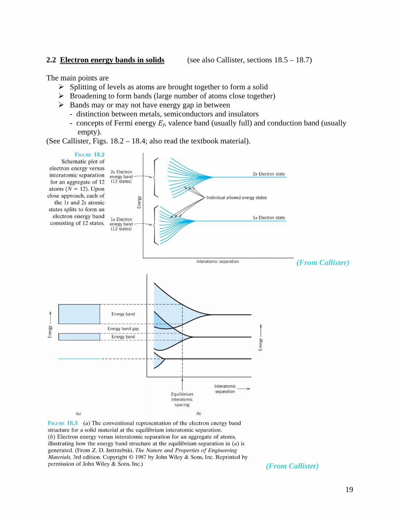
2.2 Electron energy bands in solids (see also Callister, sections 18.5 – 18.7) The main points are
Splitting of levels as atoms are brought together to form a solid Broadening to form bands (large number of atoms close together) Bands may or may not have energy gap in between
- distinction between metals, semiconductors and insulators - concepts of Fermi energy Ef, valence band (usually full) and conduction band (usually empty).
(See Callister, Figs. 18.2 – 18.4; also read the textbook material).
(From Callister)
(From Callister)
19

(From Callister) All this implies different conduction processes in − metals
− semiconductors or insulators. In the latter materials, the electrons have to be excited by a large amount of energy corresponding to the band gap. This is not the case for metals, where there are available states just above the Fermi Energy Ef (representing the energy level up to which the electron states are filled). (See Callister, Figs. 18.5 – 18.6; also read the textbook material).
(From Callister)
(From Callister)
20

Electron mobility When an electric field E is applied, scattering events (“collisions” of electrons with atoms, etc) take place in the solid, so eventually electrons acquire a drift velocity vd (proportional to the size of E) – see Callister, Fig. 18.7.
(From Callister)
E
We can define vd = µe E , where the constant of proportionality µe is the electron mobility (units are m2/V-s). From this, we can work out the current flow and obtain the conductivity σ. The result is σ = n |e| µewhere n is the number of electrons per unit volume that are free to move. To prove this, consider the charges flowing across a unit area: in a unit time they sweep out a distance equal to vd. Volume swept out = 1 vd ∴ No. of charges = n vd
∴ current | |area d
IJ e= = nv
So σ = J/E = |e| n vd /E = n |e| µe (where the last step follows from the definition of mobility). 2.3 Metals (see also Callister, section 18.8)
The above formula for σ (= 1/ρ) holds well. Values of n and µe do not vary enormously between different metals, and so values of σ tend to have same order of magnitude. (See Table 18.1).
(From Callister)
21
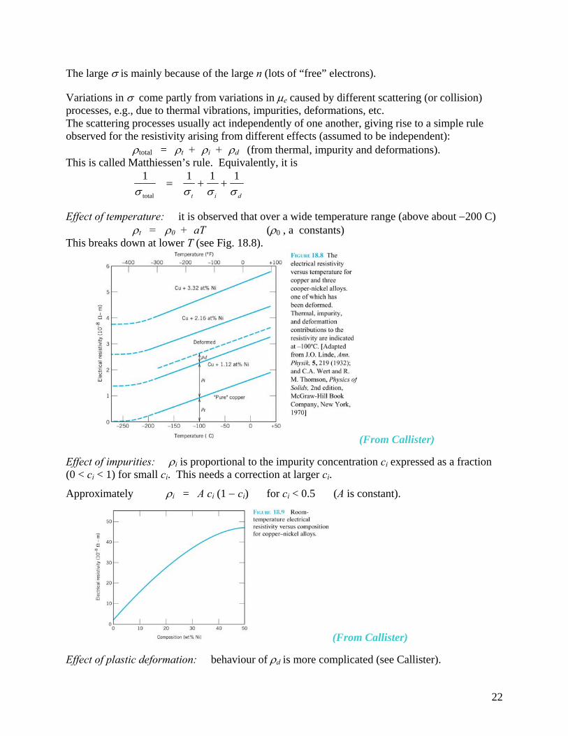
The large σ is mainly because of the large n (lots of “free” electrons). Variations in σ come partly from variations in µe caused by different scattering (or collision) processes, e.g., due to thermal vibrations, impurities, deformations, etc. The scattering processes usually act independently of one another, giving rise to a simple rule observed for the resistivity arising from different effects (assumed to be independent): ρtotal = ρt + ρi + ρd (from thermal, impurity and deformations). This is called Matthiessen’s rule. Equivalently, it is
total
1 1 1
t i d
1σ σ σ σ
= + +
Effect of temperature: it is observed that over a wide temperature range (above about −200 C) ρt = ρ0 + aT (ρ0 , a constants) This breaks down at lower T (see Fig. 18.8).
(From Callister)
Effect of impurities: ρi is proportional to the impurity concentration ci expressed as a fraction (0 < ci < 1) for small ci. This needs a correction at larger ci.
Approximately ρi = A ci (1 − ci) for ci < 0.5 (A is constant).
(From Callister)
Effect of plastic deformation: behaviour of ρd is more complicated (see Callister).
22

2.4 Semiconductors (see also Callister, sections 18.10−18.14) Their electrical properties are sensitive to even minute amounts of impurities (often this is used to great advantage for devices). Allows for the following distinction in behaviour:
intrinsic semiconduction – where σ depends on electronic structure of the pure material extrinsic semiconduction – where the behaviour of σ is strongly influenced by impurities
The main classes of semiconductor materials are:-
Elemental semiconductors – Si, Ge Found in Group IVA of periodic table; have covalent bonding III-V compounds – e.g., GaP, GaAs, InSb
Formed between elements of Groups IIIA and VA II-VI compounds – e.g., CdS, ZnTe
Formed between elements of Groups IIB and VIA.
(From Callister) An important parameter is energy band gap Eg between the valence band and conduction band. Eg ~ 1.11 eV for Si Eg ~ 0.67 eV for Ge For most compound semiconductors Eg ~ 1.0 to 2.5 eV (the slightly higher values are often associated with increased tendency to ionic bonding). If Eg is any larger, we have an insulator. Concept of a hole: In an intrinsic (pure) semiconductor, for every electron that is excited into the conduction band, there is a vacant (or “missing”) electron at the top of the conduction band:
23

Conduction band (empty initially) Eg Valence band (filled initially) We have: an electron in the conduction band + absence of an electron in the valence band. This vacancy behaves and moves (e.g., when an electric field is applied) like a positive charge of the same mass as an electron in the solid. Intrinsic conductivity
This is for highly pure materials (negligible effect of any impurities).
Conductivity occurs by the mechanism just discussed: electrons are thermally excited from the filled valence band (leaving holes) to the conduction band. Thus there are 2 types of charges to contribute to σ (the electrons and the holes). See Callister, Fig. 18.10.
(From Callister)
24

The previous expression that σ = n |e| µe (as used for metals) now generalizes to σ = n |e| µe + p |e| µh
where p is the number of holes per unit volume and µh is the hole mobility. The two terms are additive. In the present case we have n = p (we call this value the intrinsic carrier concentration ni), so σ = ni |e| (µe + µh) It turns out that we always have µe > µh (electrons are easier to move than holes). How big is the ni term? Example. Calculate ni for intrinsic GaAs given σ = 1 × 10⁻⁶ (Ω-m) −1 , µe = 0.85 m2/V-s and µh = 0.04 m2/V-s (all values at room temperature).
Answer. ni = 6
1219
10 7.0 10| | ( ) (1.6 10 )(0.85 0.04)e he
σµ µ
−
−= =+ × +
× m−3
Extrinsic conductivity
− This is applicable when there are selected impurities with concentrations comparable to (or larger than) the calculated ni.
There are 2 cases of interest, called n-type and p-type. 1) n-type extrinsic semiconductors As an example, consider Si. Each atom has 4 valence electrons, each of which bonds covalently with one electron of 4 neighbouring Si atoms (as in Fig. 18.10). Suppose now that an impurity atom of valence 5 is added as a substitutional impurity (some possibilities are the Group VA elements P, As or Sb).
→ The extra non-bonding electron is left over and is only weakly attached. Thus it can move if an electric field is applied, and a current will flow.
→ Its energy level comes inside the band gap, just below the conduction band; it is called a donor impurity level.
See also Callister, Figs. 18.11 and 18.12.
25

(From Callister)
(From Callister) Notice that the process does not cause any holes to be formed in the valence band. ∴ n >> p in this case (and hence the name n-type) For the conductivity, σ ≅ n |e| µe , and the electrons are called the majority carriers.
26

2) p-type extrinsic semiconductors
We again use Si as an example, but in this case we add a substitutional impurity that has valence 3 from group IIIA (e.g. Al, B, or Ga). This produces the opposite effect to the previous case: there is now a deficiency of one electron in one of the covalent bonds
→ This is like having one hole that is only loosely attached. → It’s energy level again comes within the band gap, but it is now just above the
valence band. It is called an acceptor impurity level. See also Callister, Figs. 18.13 and 18.14.
(From Callister)
(From Callister) This process leaves holes at the top of the valence band, but it does not form electrons in the conduction band. ∴ p >> n in this case (and hence the name p-type) We have σ ≅ p |e| µh , and the holes are called the majority carriers.
The process of intentionally adding the impurities to form n-type or p-type semiconductors as an alloy is called doping. Temperature dependence of σ in semiconductors
— this comes from the T-dependence of the carrier concentrations (n and/or p) and the T-dependence of the mobilities (µe and/or µh)
— the behaviour for the intrinsic and extrinsic situations can be discussed with reference to Callister, Figs. 18.15-15.18)
27
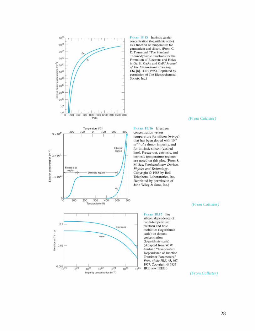
(From Callister)
(From Callister)
(From Callister)
28

(From Callister) 8.5 Semiconductor devices (see also Callister, section 18.15) The need for devices is driven by applications such as computer memory storage, fast switching at low power levels, etc. It has led to development of nanometer size devices in some cases, e.g. as integrated circuits on a chip. Three basic devices will be described here:-
• p-n junctions — these can rectify signals (allow current flow in just one direction)
• junction transistors — these can amplify signals and provide switching • MOSFET (transistors) — these can amplify signals and provide switching
(a) p-n junction This acts as a diode — it is a 2-terminal device where the current flow is easier in one direction compared with the other. So it can be used to rectify ac signals. Basically it consists of a single piece of a semiconductor material where one half is doped p-type and the other half is doped n-type.
A voltage supply can be connected in an external circuit in eitherforward bias — (+ve battery terminal to p side, −ve battery terminal to n-side) orreverse bias — (the opposite to the above)
29

In forward bias, electrons and holes move towards each other and mostly recombine (annihilating each other): el + hole → energy. A current can flow in the external circuit.
In reverse bias, electrons and holes move apart, leaving a region with almost no charge carriers, so it acts like an insulator (→ very little current)
See Callister, Figs. 18.19 – 18.21 to illustrate the above and the rectification process.
(From Callister)
(From Callister)
(From Callister)
30

(b) junction transistor If we form more than two doping regions in a semiconductor sample, we can achieve more complicated functions. In a transistor there are 3 terminals (3 regions) — it can be used (e.g.) as a switch or as an amplifier. In a junction transistor we sandwich an n-type layer between two p-type layers (or vice-versa) to form: p – n – p (or n – p – n)
See Callister, Fig. 18.22 and 18.23.
(From Callister)
The mode of operation is to make one junction forward biased and the other reverse biased. The base region (in the centre – see Fig. 18.22) is designed to be sufficiently thin (and with the optimum doping level) so that most of the charges are swept right through.
(From Callister) (c) MOSFET This is an example of a Field Effect Transistor. The MOS stands for Metal-Oxide Semiconductor. In a p-type device there are two p-type regions formed near a surface and surrounded by n-type material. A thin connecting channel of p-type material is formed between the p-type regions. An
31

oxide insulating film is deposited on the surface and metal contacts are formed (using etching) to give contacts to the p-type regions. Another metal contact on top of the insulating film, but adjacent to the channel, can have a bias voltage applied either to attract or repel holes. See Callister, Fig. 18.24 for the mode of operation.
(From Callister) 8.6 Other electrical properties (see also Callister, section 18.24 and 18.25) Two other electrical effects that can occur in a few compound materials, that have low symmetry or are distorted, are ferroelectricity and piezoelectricity. Ferroelectricity This is somewhat analogous to ferromagnetism (where a magnetic moment or magnetization occurs spontaneously below a critical temperature TC).
The difference is that, in ferroelectric materials, there is a spontaneous electric-dipole moment below some temperature TC. It vanishes for T > TC. It is associated with a distortion of the crystal lattice in an ionic material (so oppositely charged ions move relative to one another) — it sets in below some critical temperature and is absent (destroyed by the thermal energy) above that temperature. Examples are: BaTiO3 with TC ~ 120 C (see Fig. 18.26),
and KH2PO4 (known as KDP) These materials can have extremely high dielectric constants (useful e.g. in capacitors).
32
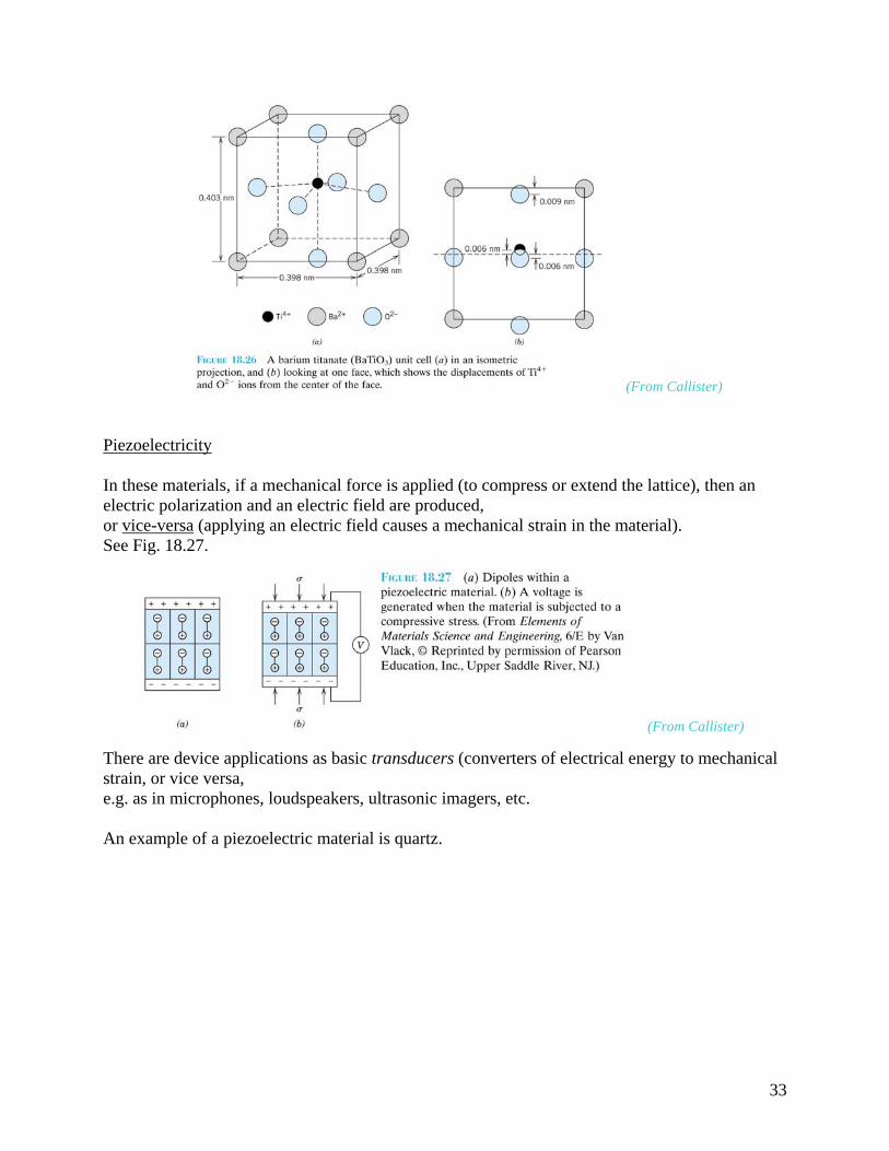
(From Callister) Piezoelectricity In these materials, if a mechanical force is applied (to compress or extend the lattice), then an electric polarization and an electric field are produced, or vice-versa (applying an electric field causes a mechanical strain in the material). See Fig. 18.27.
(From Callister) There are device applications as basic transducers (converters of electrical energy to mechanical strain, or vice versa, e.g. as in microphones, loudspeakers, ultrasonic imagers, etc. An example of a piezoelectric material is quartz.
33