
Outline
18
Silicon Strip Detectors for the ATLAS HL-LHC Upgrade Paul Dervan The University of Liverpool On behalf of the ATLAS Upgrade Community PSD09, 12th-16th September 2011, Aberystwyth 1
-
Upload
justina-pearson -
Category
Documents
-
view
27 -
download
0
description
Silicon Strip Detectors for the ATLAS HL-LHC Upgrade Paul Dervan The University of Liverpool On behalf of the ATLAS Upgrade Community. Outline. Introduction to the Upgrade Layout Si Sensors Design Performance Hybrid Modules Performance Staves. PHASE 1. PHASE 2. 2000-3000. PHASE 0. - PowerPoint PPT Presentation
Transcript of Outline

Silicon Strip Detectors for the ATLAS HL-LHC Upgrade
Paul DervanThe University of Liverpool
On behalf of the ATLAS Upgrade Community
PSD09, 12th-16th September 2011, Aberystwyth 1

Outline
Introduction to the Upgrade
Layout
Si SensorsDesign Performance
Hybrid
Modules Performance
Staves
PSD09, 12th-16th September 2011, Aberystwyth 2
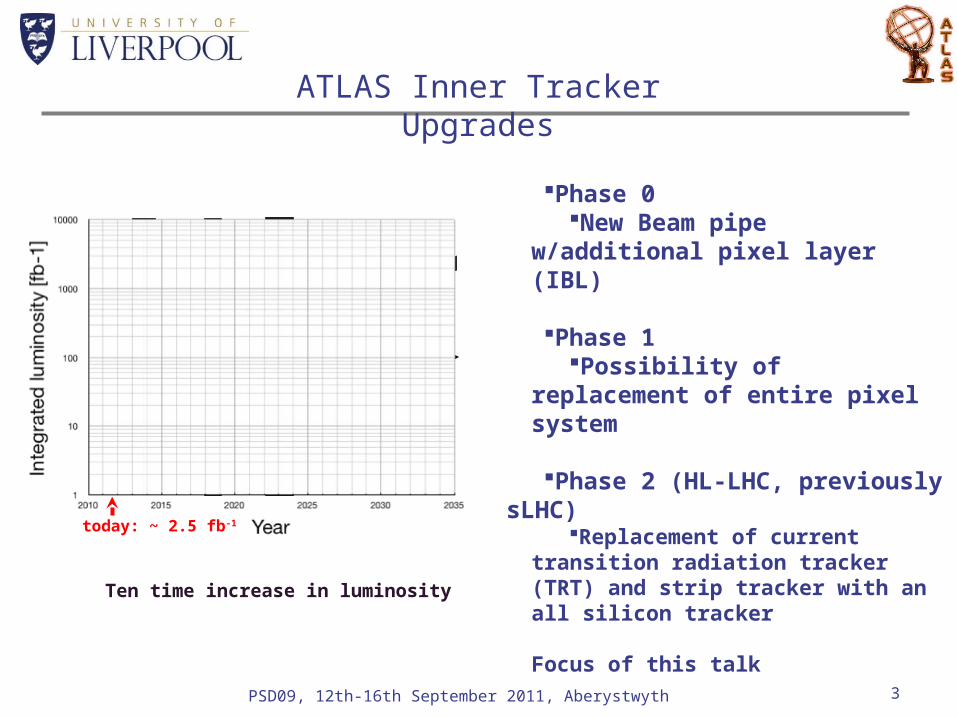
ATLAS Inner Tracker Upgrades
Phase 0New Beam pipe w/additional
pixel layer (IBL)
Phase 1Possibility of replacement of
entire pixel system
Phase 2 (HL-LHC, previously sLHC)
Replacement of current transition radiation tracker (TRT) and strip tracker with an all silicon tracker
Focus of this talk
PH
AS
E 0
LHC shutdown
PH
AS
E 1
PH
AS
E 2
5-10
100-200
200-400
2000-3000
today: ~ 2.5 fb-1
HL-LHCHL-LHC
PSD09, 12th-16th September 2011, Aberystwyth 3
Ten time increase in luminosity

ATLAS Phase II Tracker Upgrade
Pixels
Short Strips
Long Strips
PSD09, 12th-16th September 2011, Aberystwyth 4
Challenges facing HL-LHC silicon detector upgrades:
• Higher occupancies⤷Finer Segmentation
• Higher particle fluences⤷ Increase Radiation
Tolerance
• Larger Area (~200 m2)⤷Cheaper Sensors Fluence estimates up to few 1016 particles/cm2
Gives Grad (10 MGy) doses to components
Fluence estimates include a 2x “safety” factor for prediction uncertainties
1 MeV neq cm2

ATLAS Phase II Tracker Upgrade
PSD09, 12th-16th September 2011, Aberystwyth 5
Short Strip (2.4 cm) -strips (stereo layers):Long Strip (4.8 cm) -strips (stereo layers):
r = 38, 50, 62 cm Up to 1.2x10¹⁵ 1MeV neq/cm2
r = 74, 100 cm Up to 5.6x10¹⁴ 1MeV neq/cm2

Radiation Hard Sensors
PSD09, 12th-16th September 2011, Aberystwyth 6
• n+-strip in p-type substrate (n-in-p)– Collects electrons like current n-in-n pixels
• Faster signal, reduced charge trapping– Always depletes from the segmented side
• Good signal even under-depleted– Single-sided process
• ~50% cheaper than n-in-n• More foundries and available capacity
world-wide
• Collaboration of ATLAS with Hamamatsu Photonics (HPK) to develop 9.75x9.75 cm2 devices (6 inch wafers)
– 4 segments (2 axial, 2 stereo), 1280 strip each, 74.5 mm pitch, ~320 mm thick
– FZ1 <100> and FZ2 <100> material studied– Miniature sensors (1x1 cm2) for irradiation
studies
n+
p- bulk
Al
SiO2
Guard RingBias Ring
p-spray/stop
p+

Full Size Sensor Evoluation
PSD09, 12th-16th September 2011, Aberystwyth 7
0.00
0.02
0.04
0.06
0.08
0.10
0 100 200 300
1/C
2[n
F-2]
-Vbias [V]
Depletion Voltage
W32 Vdep=202.5W33 Vdep=202.3W35 Vdep=201.4W37 Vdep=198.8W38 Vdep=200.3W39 Vdep=199.4W15 Vdep=245.5W16 Vdep=234.9
1 kHz with CR in Series
Specification Measurement
Leakage Current <200 µA at 600 V 200– 370nA
Full Depletion Voltage <500 V 190 – 245VCoupling Capacitance (1kHz) >20 pF/cm 24 – 30pF
Polysilicon Resistance 1.5+/-0.5MΩ 1.3 -1.6MΩ
Current through dielectric Idiel < 10 nA < 5nA
Strip Current No explicit limit < 2nAInterstrip Capacitance (100kHz) <1.1pF/cm (3 probe) 0.7 – 0.8pF
Interstrip Resistance > 10x Rbias~15 MΩ >19 GΩ
All specifications already met!!See J. Bohm, et. al., Nucl. Inst. Meth. A, Vol. 636 (2011) S104-S110 for details
0.0
1.0
2.0
3.0
4.0
0 100 200 300
Cin
t [p
F]
-Vbias
Interstrip CapacitanceW33-Seg1W33-Seg2W33-Seg3W33-Seg4W35-Seg1W35-Seg2W35-Seg3W35-Seg4W37-Seg1W37-Seg2W37-Seg3W37-Seg4W38-Seg1W38-Seg2W38-Seg3W38-Seg4W39-Seg1W39-Seg2W39-Seg3W39-Seg4W32-Seg1W32-Seg2W32-Seg3W32-Seg4
100kHz test frequency with CpG
0
100
200
300
400
500
0 200 400 600 800 1000
-Ile
ak
[n
A]
-Vbias [V]
Leakage Currentw32 PRGw33 PRGw35 PRGW37 PRGw38 PRGw39 PRGW19 SBUW21SBUW22 SBUW23 SBUW25 SBUW26 SBUW27 SBUW28 SBUW29 SBUW18 GeUW17 GeUW15 CAMW16 CAM
Ileak normalized to 20 C

Charge Collection results
PSD09, 12th-16th September 2011, Aberystwyth 8
• Miniature devices irradiated to strip barrel fluences with neutrons, pions, protons
• Charge collection measured with 90Sr b-source
– Consistent results between different groups/equipment
• S/N greater than 10:1 for strip sensor types with expected noise performance
– ~600-800 e- short strips, ~800-1000 e- long strips– See H. Sadrozinski, et.al., Nucl. Inst. Meth. A,
doi:10.1016/j.nima.2011.04.0646 for details
10:1 Signal-to-Noise
10:1 Signal-to-Noise 10:1 Signal-to-Noise
Protons Pions
Neutrons

Stave Hybrid – Layout and Electrical Detail
Hybrid is designed to accommodate 20 x ABCN-25 readout ASICs (2 columns of 10)
Layout topology matches ATLAS07 large area sensor and serially powered Bus cable ASICs placed to match sensor pitch and bond pad
profile Hybrid Power and Digital I/O bond fields at opposite
ends
Circuit exploits features of ABCN-25 Bi-directional data paths Embedded distributed shunt regulators (for serial
powering) Requires external control circuit
10PSD09, 12th-16th September 2011, Aberystwyth
Mshunt control and Digital I/O
Hybrid Power and sensor HV filtering(spec’d to 500V)

Stave Hybrid – Layout and Electrical Detail
10PSD09, 12th-16th September 2011, Aberystwyth
Design is driven by minimising material
Hybrid is substrate-less and with no connectors Glued directly on to the sensor
Provides mechanical support and thermal management
All off-module connections made via wire bonds
Use of minimal glue layers for both ASIC and hybrid attachment Improves thermal paths and again reduces material
Pitch adapters not used, direct ASIC-to-Sensor wire bonding Constrains relative placement w.r.t. sensor to better than
80µm

Stave Module Tests
PSD09, 12th-16th September 2011, Aberystwyth 11
Parallel Serial DC-DC
Hybrid 62 590 e-
596 e-590 e-
599 e-595 e-
603 e-
Hybrid 61 585 e-
591 e-588 e-
599 e-585 e-
591 e-
598e
DC-DC converters
• Stave modules are tested in PCB frames– Cheap, flexible test bed for different
power/shielding/grounding configurations
• Parallel powering, serial powering, and DC-DC converters have all been evaluated – With proper grounding/shielding, all these
configurations give expected noise performance
Hybrid 61
Hybrid 62
Se
rial P
ow
er
Ch
ain
AC
Co
up
led
C
loc
k/C
om
ma
nd
Input noise: 588e-
Input noise: 599e-
Input noise: 590e-
Input noise: 599e-
Serial Powering
Column 0
Column 1
Column 2
Column 3
Column 0
Column 1
Column 2
Column 3

Stave Module Irradiation
PSD09, 12th-16th September 2011, Aberystwyth 12
Noise Column 0 Column 1Pre-Irrad 610 e- 589 e-
Post-Irrad 675 e- 650 e-
Difference 65 e- 61 e-
Expected 670 e- 640 e-
AL Foil
AL Foil
Pre-irradiationPost-irradiation Motorized, Cooled
Irradiation Stage
• Irradiated at CERN-PS irradiation facility– 24 GeV proton beam scanned over inclined
modules– Module biased, powered, and clocked during
irradiation– Total dose of 1.9x10¹⁵ neq cm-2 achieved
• Max predicted fluence for barrel modules is 1.2x10¹⁵ neq cm-2
• Sensor and module behave as expected– Noise increase consistent with shot noise
expectations

PSD09, 12th-16th September 2011, Aberystwyth 13
Stave – Geometry and components
1200mm
Bus cable
Hybrid + Sensor
Carbon honeycomb
Carbon fiberfacing
Readout IC’s
ABCN-25 readout ASIC 40 per module 960 per stave (>120k channels)
Kapton flex hybrid with auxiliary boards BCC ASIC (multi drop & point-to-point I/O) Serial Power protection
Serial powering of modules Embedded Kapton bus cable
End of stave card Stave mechanical core
Coolant tube structure
Single flexModule with
2 x flex
120mm
Sensor
12 modules/side of stave (24 total)
Auxiliary Board(s)

Stavelet
PSD09, 12th-16th September 2011, Aberystwyth 14
AL Foil
AL Foil
Motorized, Cooled Irradiation Stage
BCC PCBs
Serial Power Protection PCBs or DC-DC Converters
Bus Cable
EOS Card
data and hybrid communication
power and power control
• Shortened stave built as electrical test-bed Shielding, grounding, serial and DC-DC powering, …
• First stavelet serial powered Power Protection Board (PPB) has automated
over-voltage protection and slow-controlled (DCS) hybrid bypassing
DC-DC stavelet under construction• Uses Basic Control Chip (BCC) for data I/O
Generates 80MHz data clock from 40MHz BC clock 160Mbit/s multiplexed data per hybrid
DC-DC converter

Serial Powered Stavelet Electrical Results
PSD09, 12th-16th September 2011, Aberystwyth 15
AL Foil
AL Foil
Motorized, Cooled Irradiation Stage
• Uses on-hybrid shunt control circuit• Stavelet noise approaching single module
tests– Roughly ~20 e- higher– Bypassing hybrids does not affect noise
performance• All technologies necessary for serial
powering of stave have been prototyped and shown to work (and compatible with 130 nm CMOS)
– Constant current source, SP protection and regulation, multi-drop LVDS
• Currently optimizing location of components, size of SP chains
• Minimal impact on material budget– Estimated to be ~0.03% averaged over
the stave
Stavelet Noise using Serial Power
Co
lum
n o
f ch
ips
Modules

Petal Endcaps
PSD09, 12th-16th September 2011, Aberystwyth 16
AL Foil
AL Foil
Motorized, Cooled Irradiation Stage
• The petal concept follows closely the barrel stave concept
• 5 discs on each end cap with 32 petals per disc– 6 Sensor rings
• First petal cores have been produced– Flat to better than 100 mm
• First endcap hybrids tested– Same performance as barrel hybrid
• n-in-p sensor prototypes submitted to CNM to make petal-let using 4” wafers
8.60 cm
8.07 cm

Alternative Solution: Super Module
PSD09, 12th-16th September 2011, Aberystwyth 17
AL Foil
AL Foil
Motorized, Cooled Irradiation Stage
• Modular concept: cooling, local structure, service bus, power interface are decoupled from the modules
• Overlapping coverage in Z• Rework – Possible up to the commissioning after
integration• Design includes carbon-carbon hybrid bridge
Hybrid could be also glued as for stave modules to reduce material

Conclusions
PSD09, 12th-16th September 2011, Aberystwyth 18
AL Foil
AL Foil
Motorized, Cooled Irradiation Stage
• The current ATLAS TRT and silicon strip tracker must be replaced with an all-silicon tracker for HL-LHC operation (planned to be assembled by 2020)
• The R&D program of components has made significant progress:– Full-size prototype planar strip detectors have already been
fabricated at Hamamatsu Photonics (HPK) which meet the final specifications
– Working baseline and alternative module prototypes have been made and shown to work after irradiation
• Full-size stave/super-module prototypes are planned to be finished this year with the next generation of the 130 nm ASICs for the strip tracker under design


![Outline Product Liability Riina Spr2009 Outline[1]](https://static.fdocuments.us/doc/165x107/54fbf0ed4a795937538b4ab9/outline-product-liability-riina-spr2009-outline1.jpg)


![[ Outline ]](https://static.fdocuments.us/doc/165x107/56815a74550346895dc7db61/-outline--56b49f971d862.jpg)