Presented and published in the Proceedings of the EuroSun ...
Originally published in the Proceedings of SMTA International, Ft. Worth, TX, October, 2013
FINE TUNING THE STENCIL MANUFACTURING PROCESS AND OTHER
STENCIL PRINTING EXPERIMENTS
Chrys Shea
Shea Engineering Services
Burlington, NJ USA
Ray Whittier
Vicor Corporation – VI Chip Division
Andover, MA USA
ABSTRACT
Previous experimentation on a highly miniaturized and
densely populated SMT assembly revealed the optimum
stencil alloy and flux-repellent coating for its stencil
printing process. Production implementation of the
materials that were identified in the study resulted in
approximately 5% print yield improvement across all
assemblies throughout the operation, validating the
results of the initial tests.
A new set of studies was launched to focus on the
materials themselves, with the purpose of optimizing
their performance on the assembly line. Using a similar
test vehicle as the prior experiments, DOEs
characterized key aspects of the stencil manufacturing
process by varying the laser cutting parameters and
coating materials. As the scope of the DOE grew, it
also included evaluation of new materials and a
comparison of microBGA aperture designs.
Eventually, additional runs were added to investigate
the effects of nanocoating on wipe frequency and
compare two different stencil cutting processes.
Results of the prior tests are reviewed, and the new test
vehicle, experimental setup and results are presented
and discussed.
BACKROUND AND INTRODUCTION
This study builds upon the results of a previous
investigation that identified the best stencil technology
for the production of a high density, highly
miniaturized PCB assembly.1 The test vehicle used in
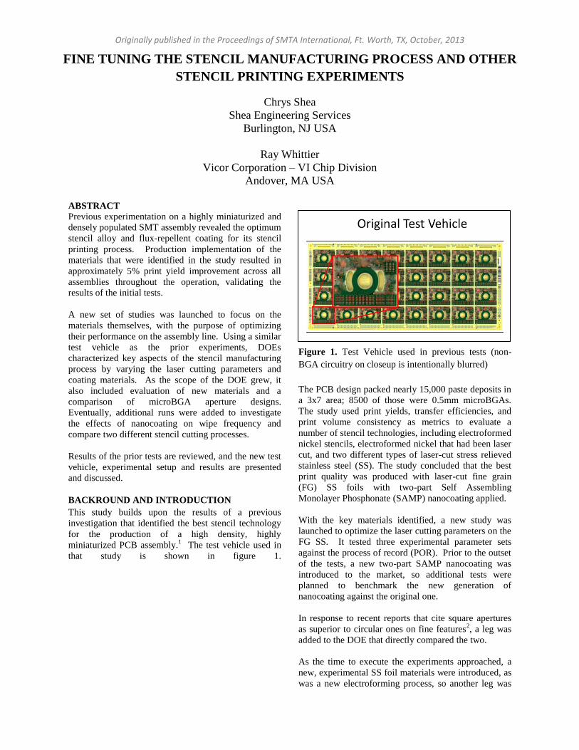
that study is shown in figure 1.
Figure 1. Test Vehicle used in previous tests (non-
BGA circuitry on closeup is intentionally blurred)
The PCB design packed nearly 15,000 paste deposits in
a 3x7 area; 8500 of those were 0.5mm microBGAs.
The study used print yields, transfer efficiencies, and
print volume consistency as metrics to evaluate a
number of stencil technologies, including electroformed
nickel stencils, electroformed nickel that had been laser
cut, and two different types of laser-cut stress relieved
stainless steel (SS). The study concluded that the best
print quality was produced with laser-cut fine grain
(FG) SS foils with two-part Self Assembling
Monolayer Phosphonate (SAMP) nanocoating applied.
With the key materials identified, a new study was
launched to optimize the laser cutting parameters on the
FG SS. It tested three experimental parameter sets
against the process of record (POR). Prior to the outset
of the tests, a new two-part SAMP nanocoating was
introduced to the market, so additional tests were
planned to benchmark the new generation of
nanocoating against the original one.
In response to recent reports that cite square apertures
as superior to circular ones on fine features2, a leg was
added to the DOE that directly compared the two.
As the time to execute the experiments approached, a
new, experimental SS foil materials were introduced, as
was a new electroforming process, so another leg was

Originally published in the Proceedings of SMTA International, Ft. Worth, TX, October, 2013
added to analyze their performance. During the
execution of the tests, two additional runs were added
to begin understanding the relationship between
nanocoating and stencil under wipe frequency.
Upon review of the results, a final run was added to
benchmark the performance of a different laser stencil
cutting process.
All the tests were executed in a similar fashion, using
the same ten-print test and the same metrics for
analysis. Detailed information on the derivation of the
Area Ratio, Transfer Efficiency and Coefficient of
Variation metrics used in this study is provided in the
original report, cites as reference #1.
EXPERIMENTAL SETUP
Test Vehicle
The original test vehicle shown in figure 1 was used for
a multitude of comparative tests over a two-year span.
It is a production PCB that offers vast amounts of
comparative data. The design was recently revised; the
new test vehicle used in this evaluation is shown in
Figure 2.
Figure 2. New Test Vehicle.
This new design replaced some of the microBGAs with
FETs, reducing the number of BGA I/Os from 8500 to
2176 per board. The number of 0201s increased on this
design, from 1900 deposits per print to 3712. A ten-
print test using the new TV now produces 21,760 BGA
data points and 37,120 0201 data points.
Test Methods
For each stencil, 10 prints were produced sequentially
on a well maintained and calibrated 2009 DEK horizon
stencil printer using, both front-to-back and back-to-
front squeegee strokes, with an automatic dry wipe after
each print. Print parameters were:
Print speed: 7 mm/sec
Print pressure: 8 kg (250mm blades)
Separation speed: 20mm/sec
Wipe sequence vacuum/dry/vacuum
The solder paste used in all tests was Indium 3.2 HF
Type 3, water soluble, lead-free, halogen-free, lot
numbers PS52867 and PS54561. Fresh paste was used
on each stencil. The paste was not kneaded; 2 dummy
prints were produced before measurements were taken.
The 17 stencils were print tested in a climate controlled
NPI manufacturing area over 9 different runs. During
the tests the room temperature ranged from 22.0 to
25.3°C, and relative humidity ranged from 36.3 to
42.9%.
The PCB was supported with a flat, non-vacuum
tooling plate and edge clamps. Deposit volume
measurements were taken with a Koh Young 3020VAL
using a Bare Board Teach to set the reference plane.
Test Matrices
All the experimental stencils were produced by the
same supplier. Their thickness was specified at 4mil.
The laser cut stencils were all produced on the same
cutter within a two-week period. The first-generation
nanocoating, Nano1, (DEK NanoProTek) was applied
to the specified stencils at the supplier’s site; second-
generation coating, Nano2, (Aculon NanoClear) was
applied at the test site. The designs of the individual
experiments are listed in tables 1-4.
Table 1. Laser cutting parameter experiment
Stencil # Description
1 POR with Nano1
1a POR w/o Nano
2 Param Set 1 with Nano1
2a Param Set 1 w/o Nano
3 Param Set 2 with Nano1
3a Param Set 2 w/o Nano
4 Param Set 3 with Nano1
4a Param Set 3 w/o Nano
Experiment #1
Compare Cutting Parameters on FG SS
Originally published in the Proceedings of SMTA International, Ft. Worth, TX, October, 2013
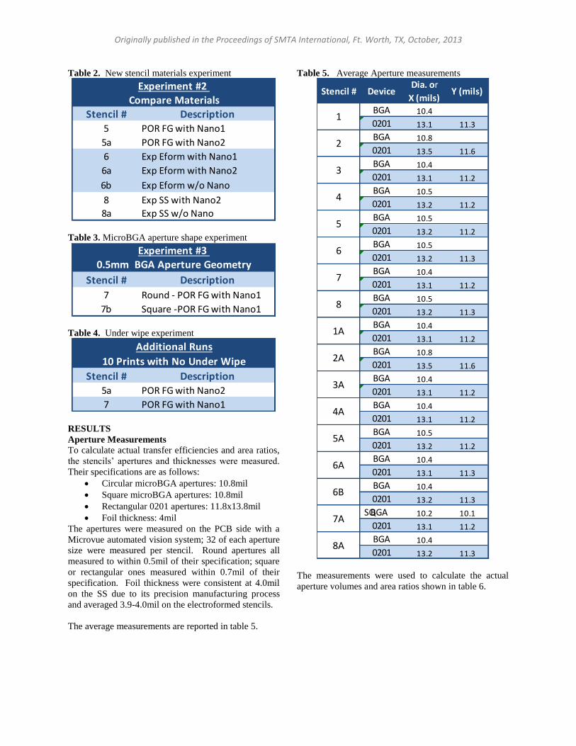
Table 2. New stencil materials experiment
Table 3. MicroBGA aperture shape experiment
Table 4. Under wipe experiment
RESULTS
Aperture Measurements
To calculate actual transfer efficiencies and area ratios,
the stencils’ apertures and thicknesses were measured.
Their specifications are as follows:
Circular microBGA apertures: 10.8mil
Square microBGA apertures: 10.8mil
Rectangular 0201 apertures: 11.8x13.8mil
Foil thickness: 4mil
The apertures were measured on the PCB side with a
Microvue automated vision system; 32 of each aperture
size were measured per stencil. Round apertures all
measured to within 0.5mil of their specification; square
or rectangular ones measured within 0.7mil of their
specification. Foil thickness were consistent at 4.0mil
on the SS due to its precision manufacturing process
and averaged 3.9-4.0mil on the electroformed stencils.
The average measurements are reported in table 5.
Table 5. Average Aperture measurements
The measurements were used to calculate the actual
aperture volumes and area ratios shown in table 6.
Stencil # Description
5 POR FG with Nano1
5a POR FG with Nano2
6 Exp Eform with Nano1
6a Exp Eform with Nano2
6b Exp Eform w/o Nano
8 Exp SS with Nano2
8a Exp SS w/o Nano
Experiment #2
Compare Materials
Stencil # Description
7 Round - POR FG with Nano1
7b Square -POR FG with Nano1
Experiment #3 0.5mm BGA Aperture Geometry
Stencil # Description5a POR FG with Nano2
7 POR FG with Nano1
Additional Runs
10 Prints with No Under Wipe
Stencil # DeviceDia. or
X (mils)Y (mils)
11.2
11.3
11.3
10.1
11.213.1
10.4
13.1
10.4
13.2
10.4
13.2 11.3
11.2
11.3
11.2
11.6
11.2
11.2
13.2
10.2
13.5
10.4
13.1
10.4
13.1
10.5
10.4
13.1
10.5
13.2
10.4
13.1
10.5
13.2 11.2
10.5
13.2 11.3
11.6
10.4
13.1 11.2
10.5
13.2 11.2
6BBGA
0201
10.4
13.1 11.3
10.8
13.5
10.8
7ASQBGA
0201
8ABGA
0201
5ABGA
0201
6ABGA
0201
3ABGA
0201
4ABGA
0201
1ABGA
0201
2ABGA
0201
7BGA
0201
8BGA
0201
5BGA
0201
6BGA
0201
3BGA
0201
4BGA
0201
1BGA
0201
2BGA
0201

Originally published in the Proceedings of SMTA International, Ft. Worth, TX, October, 2013
Table 6. Aperture volumes and area ratios for test
stencils
Paste Volume Measurements & Print Yields
The paste volume information and print yields resulting
from the 10-print tests are shown in tables 7-9.
Table 7. Measured Print Volume Results for
microBGAs and Print Yields
Table 8. Measured Print Volume Results for 0201s at
0 degree orientation and Print Yields
Stencil #Device
Type
Volume
(cu mil)
Area
Ratio
337 0.65
592 0.76
366 0.67
627 0.78
342 0.65
590 0.76
344 0.65
593 0.76
344 0.65
593 0.76
343 0.65
595 0.76
337 0.65
587 0.75
346 0.66
599 0.76
342 0.65
589 0.76
365 0.67
627 0.78
341 0.65
589 0.76
341 0.65
586 0.75
343 0.65
593 0.76
341 0.65
592 0.76
340 0.65
594 0.76
410 0.63
589 0.76
340 0.65
595 0.76
7ASQBGA
0201
8ABGA
0201
5ABGA
0201
6ABGA
0201
3ABGA
0201
4ABGA
0201
1ABGA
0201
2ABGA
0201
7BGA
0201
8BGA
0201
5BGA
0201
6BGA
0201
3BGA
0201
4BGA
0201
1BGA
0201
2BGA
0201
6BBGA
0201
Aperture Stencil Mean Std dev CV YIELD
1 344 31 9% 80%
1A 273 31 11% 60%
2 306 30 10% 80%
2A 306 34 11% 70%
3 273 35 13% 90%
3A 302 43 14% 70%
4 313 50 16% 0%
4A 289 42 15% 60%
5 285 41 14% 80%
5A 278 34 12% 80%
5A-No Wipe 288 31 11% 90%
6 282 33 12% 60%
6A 295 32 11% 100%
6B 307 42 14% 70%
7 279 44 16% 70%
S7-No Wipe 297 35 12% 100%
7A 358 41 11% 70%
8 298 34 11% 100%
8A 311 37 12% 90%
BG
As
Aperture Stencil Mean Std dev CV YIELD
1 717 67 9% 80%
1A 632 71 11% 60%
2 618 65 11% 80%
2A 635 77 12% 70%
3 582 69 12% 90%
3A 611 82 14% 70%
4 631 93 15% 0%
4A 597 88 15% 60%
5 589 84 14% 80%
5A 584 67 11% 80%
5A-No Wipe 593 61 10% 90%
6 579 77 13% 60%
6A 606 68 11% 100%
6B 604 77 13% 70%
7 586 90 15% 70%
S7-No Wipe 600 66 11% 100%
7A 603 72 12% 70%
8 609 66 11% 100%
8A 631 72 11% 90%
02
01
s at
0 d
egr
ee
s

Originally published in the Proceedings of SMTA International, Ft. Worth, TX, October, 2013
Table 9. Measured Print Volume Results for 0201s at
00 degree orientation and Print Yields
SPI databases were also queried for the microBGAs
average positional offset in X and Y. The results are
shown in Table 10.
Table 10. Average positional offset of microBGA
prints
ANALYSIS
Experiment #1 - Effect of Cutting Parameters and
Nanocoating
1) Print Yields
Print yields are determined by the automatic solder
paste inspection system. All 9472 deposits must fall
within their specified ranges for the print to be
considered a pass. As little as one deposit out-of-spec
will cause the print to be a fail.
The print yields are show in figure 3. With the
exception of parameter set 3, the treated stencils yielded
10-20% better than the untreated ones. Additionally,
parameter set 2 produced the highest yields. The
treated stencil in Parameter set 3 yielded 0% due to a
miscut aperture (figure 4).
Figure 3. Effect of cutting parameters and nanocoating
treatment on print yields.
Figure 4. Miscut stencil aperture on stencil 4.
Aperture Stencil Mean Std dev CV YIELD
1 694 63 9% 80%
1A 608 67 11% 60%
2 595 64 11% 80%
2A 611 75 12% 70%
3 564 66 12% 90%
3A 591 81 14% 70%
4 608 95 16% 0%
4A 579 86 15% 60%
5 567 80 14% 80%
5A 562 63 11% 80%
5A-No Wipe 571 59 10% 90%
6 551 79 14% 60%
6A 583 70 12% 100%
6B 591 79 13% 70%
7 569 86 15% 70%
S7-No Wipe 582 64 11% 100%
7A 580 70 12% 70%
8 590 64 11% 100%
8A 612 72 12% 90%
02
01
s at
90
de
gre
es
Stencil X(mils) Y(mils)
1 0.44 -0.41
1a 0.46 0.39
2 0.09 0.67
2a 0.52 0.14
3 0.44 0.35
3a 0.52 0.60
4 0.60 0.66
4a 0.53 0.69
5 0.48 0.71
5a 0.57 0.37
6 0.69 0.95
6a 0.37 0.88
6b 0.58 0.86
7 0.40 0.63
7a 0.47 0.41
8 0.48 0.53
8a 0.55 0.40
PRODUCTION 0.41 0.00
Postional Offsets

Originally published in the Proceedings of SMTA International, Ft. Worth, TX, October, 2013
2) Transfer Efficiency
Transfer efficiencies (TE) are the ratio of the volume of
the measured deposit to the volume of the stencil
aperture and are expressed as a percent, or, more simply
put, the percentage of solder paste that releases from the
aperture. The aperture volumes used in the calculations
are computed based on the average measured aperture
dimension and stencil thickness, not on their
specifications.
The data from parameter set 3 were not included in
transfer efficiency or repeatability comparisons due to
the miscut aperture.
Figure 5. Effect of cutting parameters and coating on
transfer efficiency. The higher the TE, the better.
Figure 6. Effect of cutting parameters and coating on
transfer efficiency of 0201s oriented at 0 degrees.
Most of the stencils transferred about 80% for BGAs
(figure 5) and 100% for 0201’s. Figure 6 shows the TE
results for 0201s oriented at 0 degrees; similar results
were found at 90 degree orientation (not shown). No
significant difference in transfer efficiency was noted
with the different cutting parameters, with the exception
of the POR sample. The treated stencil that was cut at
the POR parameters appears to have 100% TE for the
BGAs and 120% for the 0201s. Years of baseline data
indicate mean TEs of approximately 80% and 100% for
the two device types, respectively. At the BGA’s 0.65
area ratio, 100% TE is not realistic; neither is 120% for
the 0201s. Therefore, special causes of the anomalous
data were investigated.
Positional inaccuracy, the most likely possible cause of
excess solder volumes, was investigated first. The
positional accuracy was found to be within 0.5mil in
both X and Y directions, so it was ruled out as a root
cause. The investigation then turned to the bottom of
the stencil, where numerous topographical features
were observed (figure 7). Small bits of metal fused to
the bottom of the stencil appear to have separated the
stencil from the PCB, preventing good gasketing. The
origin of these features is unknown. Closer inspection
of stencil 4 indicates that similar features may be a
contributor to the miscut aperture (fig 4).
Figure 7. Topographical features found on the PCB
side of stencil 1.
3) Volume Repeatability
Print volume repeatability is measured by dividing the
standard deviation of the print volume readings by the
mean of the readings, and is also known as the
Coefficient of Variation. It is expressed here as a
percentage. The effect of the cutting parameters and
coatings on volume repeatability is shown in figure 8.

Originally published in the Proceedings of SMTA International, Ft. Worth, TX, October, 2013
Figure 8. Effect of cutting parameters and coating on
print volume variation. The lower the CV, the better.
Parameter set 2, which offered highest yields in this
test, also produced the highest variation, which is
undesirable. Historical data indicates CVs of
approximately 10%, which is the benchmark for the
BGA device. Interestingly, the CV for stencil 1, the
one with the metal projections on the bottom side, was
the lowest of the test and slightly lower than the
benchmark. The CVs for the 0201s were nearly
identical to those of the BGAs and are not shown.
Regardless of cutting parameters, stencils treated with
nanocoating consistently provided better print volume
repeatability than those without.
Experiment #2 – New Stencil Materials
1) Print Yields The FG SS with both the first and second-generation
nanocoatings produced 80% yield. The experimental
SS without nanocoating produced 90% print yield, and
with the new generation nanocoating produced a 100%
print yield. The experimental electroform (EF) stencil
with the new nanocoating also produced 100% print
yield, but the experimental EF stencils with first-
generation or no nanocoating only produced 60 and
70% yields, respectively. Print yields for the different
materials and coating are compared in figure 9.
Figure 9. Effects of stencil alloy and coating on print
yields.
2) Transfer Efficiency
All stencils tested transferred at least 80% on the
microBGAs and close to 100% on the 0201s. Figure 10
shows the microBGA results. The experimental SS and
EF stencils without any nanocoating at all transferred
91 and 92% respectively, approximately 10% higher
than the production process. The same materials with
second-generation nanocoating released more than
86%, a less substantial yet noteworthy 5% increase
from the benchmark. The other stencils performed in
the expected 81-83% range.
Figure 10. Effects of stencil alloy and coating on BGA
transfer efficiency.
The TE of the 0201s hovered around 100%, with the
untreated experimental materials showing the highest
release, and the treated materials showing the second
highest. The trend shown in figure 11 is identical to
that of the microBGAs. Another repetitive trend
observed in all print tests is the slightly higher TE (3-
6%) for components oriented at 0 degrees versus those
oriented at 90%.
Figure 11. Effects of stencil alloy, coating and
component orientation on 0201 transfer efficiency.

Originally published in the Proceedings of SMTA International, Ft. Worth, TX, October, 2013
3) Variation
The lowest CV for the microBGAs was on the
experimental EF stencil coated with second-generation
nanocoating, at 10.8%. The next lowest was the
experimental SS with the second-generation
nanocoating (figure12) at 11.4%. This trend is again
observed in the 0201 CV data, but transposed, with the
Nano2 experimental SS at 10.9 and the Nano2
experimental EF at 11.3% (figure 13). The remainder
of the stencils all produced higher variation.
Figure 12. Effects of stencil alloy and coating on BGA
volume repeatability.
Figure 13. Effects of stencil alloy, coating and
component orientation on 0201 volume repeatability.
Experiment #3 – microBGA Aperture Shape
To compare the influence of microBGA aperture shapes
on print quality, two stencils were produced with
identical aperture geometries for all devices except the
BGAs. One stencil had specified 10.8mil circles; the
other specified 10.8mil squares with radiused corners.
1) Print Yields
Print yields for both stencils were 70%. They are not
depicted graphically.
2) Transfer Efficiency
Figure 14 shows the transfer efficiency for both
aperture shapes. The square aperture has a higher
percentage of paste transfer; it also has a higher volume
of paste due to its geometry. The average paste volume
deposited from the square aperture is approximately
358mil3, whereas the average paste volume deposited
by the round apertures was 298mil3. The square
aperture deposits an average of 22% more solder paste
than the round one.
Figure 14. Effect of microBGA aperture shape on
transfer efficiency.
3) Variation
The square aperture design also provided better print
volume consistency than the round design, as shown in
figure 15.
Figure 15. Effect of aperture shape on volume
repeatability
Summary of Round vs. Square Aperture Design
Round apertures are the process of record for these
0.5mm microBGA devices. The results of this
experiment indicate that the square apertures:
a) provide 20% more solder paste volume
b) increase transfer efficiency from 83% to 87%
c) lower variation from 16% to 11%
The effect of the increased paste volume on reflow
yields is unknown at this time. The square aperture
22
% m
ore
vo
lum
e
22
% m
ore
vo
lum
e

Originally published in the Proceedings of SMTA International, Ft. Worth, TX, October, 2013
design will be implemented on a single product and
reflow yields will be closely monitored to quantify the
aperture’s impact on the overall SMT process.
Experiment #4 – Wipe Frequency
The production print process for this product utilizes a
dry/vacuum/dry wipe after every print. The 1 print per
wipe interval was set by prior experimentation. To
test claims of nanocoating extending wipe frequencies,
additional 10-print tests with stencils 5 and 7 were
performed without any wipes at all. Both stencils were
the FG SS cut with the POR; stencil 5 used first-
generation nanocoating; stencil 7 used second-
generation nanocoating.
1) Print Yields
Print yields improved when the wiping step was
eliminated from each print. Running 10 consecutive
prints without wiping increased the print yields from 80
to 90% on stencil 5 and from 90 to 100% on stencil 7,
as shown in figure 16.
Figure 16. Effect of extending wipe frequency on print
yields
2) Transfer Efficiency
Stencil prints at the extended wipe interval showed
slightly higher transfer efficiency, as shown in figure
17.
Figure 17. Effect of extending wipe frequency on
transfer efficiency
3) Variation
In both cases, the processes that extended the wipe
intervals showed the least variation. The trend of the
second-generation nanocoating to consistently produce
less variation than the first continued, as observed in
other comparisons and shown in figure 18.
Figure 18. Effect of extending wipe frequency on
volume repeatability.
FOLLOW UP TESTS
The results of these tests and comparisons show distinct
differentiation between experimental inputs and
consistent trends among its outputs. They appear to
serve as good relative indicators of performance.
However, a considerable difference was observed in
comparison to the prior round of tests and typical
production results.
The test vehicle is a production product, and
historically runs 98.2% print yields. It also consistently
produces about 82% TE with less than 10% CV. The
relatively low yield numbers, combined with the higher
variation produced in this set of tests, indicated a
considerable process difference somewhere in the
experiment. The sources of variation were explored.
Originally published in the Proceedings of SMTA International, Ft. Worth, TX, October, 2013
First, the test setup and equipment were investigated via
a database search. The test runs always took place on
after the first shift finished using the printer, over a
course of two weeks. Investigation into the production
print yields indicated no out-of-control situations on the
assembly line during that time period; print yields for
all production prints run on that line were within in
their typical 98%+ range. The likelihood of the printer
or print test method introducing the variation was
unlikely.
Next, the performance of the stencils cut according to
the POR – 1,5 and 7 were compared. Issues had
already been identified with stencil 1’s PCB side
topography that produced atypical results, but stencils 5
and 7 did not produce results comparable with each
other (stencil 7 had the highest CV of the tests). These
stencils were all manufactured using the Process of
Record, with one exception: the usual production
stencils are manufactured at a local facility, whereas the
test stencils were produced at one of the supplier’s
other sites.
To explore the possibility of differences in the two
sites’ manufacturing processes, the production stencil
for this PCB was print tested using the same 10-print
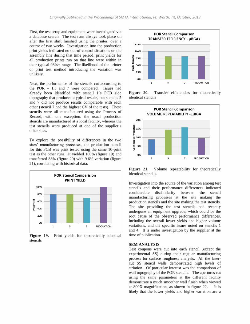
test as the other runs. It yielded 100% (figure 19) and
transferred 83% (figure 20) with 9.6% variation (figure
21), correlating with historical data.
Figure 19. Print yields for theoretically identical
stencils
Figure 20. Transfer efficiencies for theoretically
identical stencils
Figure 21. Volume repeatability for theoretically
identical stencils.
Investigation into the source of the variation among test
stencils and their performance differences indicated
considerable dissimilarity between the stencil
manufacturing processes at the site making the
production stencils and the site making the test stencils.
The site providing the test stencils had recently
undergone an equipment upgrade, which could be the
root cause of the observed performance differences,
including the overall lower yields and higher volume
variations, and the specific issues noted on stencils 1
and 4. It is under investigation by the supplier at the
time of publication.
SEM ANALYSIS
Test coupons were cut into each stencil (except the
experimental SS) during their regular manufacturing
process for surface roughness analysis. All the laser-
cut SS stencil walls demonstrated high levels of
striation. Of particular interest was the comparison of
wall topography of the POR stencils. The apertures cut
using the same parameters at the different facility
demonstrate a much smoother wall finish when viewed
at 800X magnification, as shown in figure 22. It is
likely that the lower yields and higher variation are a

Originally published in the Proceedings of SMTA International, Ft. Worth, TX, October, 2013
direct result of the rougher, more highly striated
aperture walls.
Figure 22. SEM images of aperture walls.
DISCUSSION AND CONCLUSIONS
Despite the experimental noise presumably introduced
by the different stencil manufacturing site, the trends in
the data are consistent throughout the series of tests.
Experiment #1 - Effect of Cutting Parameters and
Nanocoating
Originally, the laser cutters at the two different
manufacturing sites were assumed to produce similar
results. The considerable differences between their
outputs were not known until the print test results were
calculated and walls were examined at high
magnification. The goal of Experiment #1 – to refine
the cutting parameters to optimize stencil print
performance on the assembly line – was obviously not
reached. Even comparisons within the dataset for this
manufacturing facility were hampered by stencil
manufacturing issues on two of the four test sets;
however, one trend was abundantly clear. The stencils
treated with the first-generation nanocoating
consistently produced better yields and better print
volume variation. The nanocoated stencils
demonstrated slightly lower transfer efficiencies than
untreated stencils.
Experiment #2 – New Stencil Materials
The experimental materials treated with the second-
generation of nanocoating produced the highest yields
and best print volume repeatability.
The FG and EF stencil foils were tested with both first-
and second-generation nanocoatings, and in both cases,
the second-generation product provided better volume
repeatability.
Experiment #3 – MicroBGA Aperture Shape
Square apertures provided better release, better
repeatability, and higher print volumes than round

Originally published in the Proceedings of SMTA International, Ft. Worth, TX, October, 2013
apertures of the same major dimension (diameter = side
of square).
Experiment #4 - Wipe Frequency
Achieving 100% yields at 10 prints per wipe is a
considerable achievement. Prior to executing this test,
the concept of running this PCB to 10 prints without
wiping was completely unrealistic. The production
process wipes after every print. Previous tests on the
original test vehicle were able to successfully achieve
wipe frequencies of 3 prints per wipe using wet wipes
with solvents that were chemically matched to the
solder paste3.
Volume repeatability also improved with the extended
wipe interval. The influence of under wiping on a
stencil treated with the Nano2 is now the subject of a
current investigation.
General Comments
The stencil materials test compared current state-of-the
art materials with developmental ones, and the results
were extremely encouraging. Continued research and
development of more sophisticated materials and
manufacturing processes will help drive continued
advancements in stencil printing technology and enable
better economics in the drive for miniaturization.
The results of the nanocoating tests were as anticipated.
Lots of data has been generated over the past two years
that show the nanocoating improves print yield and
repeatability. The new nanocoating formulation’s
repeated outperformance of the original product
demonstrates real improvement in this materials
technology and is another example of materials
advancements that continue to improve stencil printing
technology.
Again in this test, the nanocoated stencils demonstrated
slightly lower transfer efficiency than non-treated
stencils. This trend was also observed in the original
tests in 2011. It is hypothesized that the lower TE of
the coated stencils may be due to crisper print
definition. This hypothesis may be tested in an
upcoming investigation.
The superior print performance of square vs circular
apertures on microBGAs was not surprising, based on
information in current literature. What was surprising
however, was the degree of improvement the square
apertures introduced. On a cautionary note, square
apertures can present gasketing issues on non-solder
mask defined pads, so they should be implemented
carefully. The PCB used in this study has solder mask
defined pads. The new aperture geometry will still be
implemented carefully, and will bear less risk than if
the PCBs were designed with non-solder mask defined
pads.
The most surprising – and most remarkable – findings
of the entire study were the wipe frequency tests on
nanocoated stencils. Not only did print yields go up, so
did volume repeatability! These results were
completely unexpected, and are currently the subject of
continued investigation.
ONGOING AND FUTURE WORK
At the time of publication, a new test had just been
executed to attempt to visualize the flux behavior on
coated and uncoated stencils with and without under
wiping. Using the original test vehicle, an uncoated
stencil (from the regular manufacturing site) was
masked and treated with Nano2 over one-half of the
print area to enable side-by-side comparison and
analysis. UV tracer was added to the solder paste, and
the PCB side of the stencil was photographed under
black light after several different print and wipe
scenarios. Photographs of some of the results are
shown in figures 23 and 24. The complete results will
be published at a future date.
ACKNOWLEDGEMENTS The authors would like to thank the stencil provider for
their participation in this study. They would also like to
recognize their colleagues who assisted in executing the
tests:
Harshal Tarar
Matthew Sawicki
Jonathan Dragonas
REFERENCES [1] Shea, C. and Whittier, R., “Evaluation of Stencil
Foil Materials, Suppliers and Coatings’” Proceedings of
SMTA International, 2011
[2] Ashmore, C., “The Changing Shape of Print
Transfer Efficiency,” Circuits Assembly Magazine,
January, 2013
[3] Lober, David, and Bixenman, Mike, et al,
“Understencil Wiping: Does it Benefit Your Process?”
Proceedings of SMTA International, 2012

Originally published in the Proceedings of SMTA International, Ft. Worth, TX, October, 2013
Figure 23. Effect of stencil nanocoating treatment on flux spread on underside of stencil, uBGA
Figure 24. Effect of nanocoating treatment on flux spread on underside of stencil, QFN

Originally published in the Proceedings of SMTA International, Ft. Worth, TX, October, 2013