Organic Electronics for a Better Tomorrow: Innovation ... · PDF fileOrganic Electronics for a...
34
Organic Electronics for a Better Tomorrow: Innovation, Accessibility, Sustainability A White Paper from the Chemical Sciences and Society Summit (CS3) San Francisco, California, United States September 2012
Transcript of Organic Electronics for a Better Tomorrow: Innovation ... · PDF fileOrganic Electronics for a...

Organic Electronics for a Better Tomorrow:
Innovation, Accessibility, Sustainability
A White Paper from the Chemical Sciences and Society Summit (CS3)
San Francisco, California, United States
September 2012

Organic Electronics for a Better Tomorrow / 1
Table of Contents
About the Chemical Sciences and Society Summit (CS3) ........................................................ 2 Foreword: Letter from the 2012 CS3 Chairs ................................................................................ 3 Executive Summary ............................................................................................................................... 4 Introduction .............................................................................................................................................. 7 Organic Electronics Today …………………………………………………………………………………10 Organic Electronics: The Vision for Tomorrow ....................................................................... 14 Research Pathway to the Future .................................................................................................... 20 Conclusion .............................................................................................................................................. 26 References .............................................................................................................................................. 27 2012 CS3 Participants ........................................................................................................................ 31

Organic Electronics for a Better Tomorrow / 2
ABOUT THE CHEMICAL
SCIENCES AND SOCIETY
SUMMIT (CS3)
The annual Chemical Sciences and
Society Summit (CS3) brings together
some of the best minds in chemical
research from around the world and
challenge them to propose innovative
solutions to society’s most pressing
needs in health, food, energy, and the
environment. This unique gathering
boasts an innovative format, aiming to
set the course of international science,
and rotates each year among
participating nations.
Organic Electronics for a Better
Tomorrow: Innovation, Accessibility,
Sustainability summarizes the outcomes
of the fourth annual 2012 CS3, which
focused on organic electronics. Thirty
top chemists and other scientists from
China, Germany, Japan, the United
States, and the United Kingdom
assembled in San Francisco to identify
major scientific and technological
research challenges that must be
addressed to advance the field of organic
electronics in a way that best meets
societal needs. This white paper presents
an international view on how the use of
organic materials in electronic devices
can contribute positively to creating a
more innovative, accessible, and
sustainable electronic world.
The CS3 initiative is a
collaboration between the Chinese
Chemical Society (CCS), German
Chemical Society (GDCh), Chemical
Society of Japan (CSJ), Royal Society of
Chemistry (RSC), and American
Chemical Society (ACS). The annual
symposia are supported by the National
Natural Science Foundation of China
(NSFC), German Research Foundation
(DFG), Japan Society for the Promotion
of Science (JSPS), UK Engineering and
Physical Sciences Research Council
(EPSRC), and U.S. National Science
Foundation (NSF).
This white paper was prepared
by science writer Leslie A. Pray, PhD, in
consultation with the American
Chemical Society, and reviewed by 2012
CS3 participants.

Organic Electronics for a Better Tomorrow / 3
FOREWORD: LETTER FROM THE
2012 CS3 DELEGATION CHAIRS
We live in an electronic world.
Economic, health, and national security
rely on and are positively impacted by
electronic technology. However, the
resources and methodologies used to
manufacture electronic devices raise
urgent questions about the negative
environmental impacts of the
manufacture, use, and disposal of
electronic devices. The use of organic
materials to build electronic devices may
offer a more eco-friendly -- and
affordable -- approach to growing our
electronic world. Moreover, and some
would say more importantly, organic
small molecules, polymers, and other
materials afford electronic structures
unique properties impossible to obtain
with silicon alone, creating untold
potential for novel functionality.
However, the field of organic
electronics is in its infancy with respect
to devices on the market. Realizing the
vision of organic electronics as a more
innovative, accessible, and sustainable
approach to growing our electronic
world will require overcoming key
research challenges.
Chemists, physicists, and other
scientists and engineers engaged in
organic electronics research representing
China, Germany, Japan, the United
Kingdom and the United States gathered
in San Francisco in September of 2012
to discuss their visions for the future of
organic electronics and to offer research
recommendations for advancing the field
in a way that will maximize its potential
positive impact on society.
Our hope is that our research
recommendations will be recognized and
considered by science policy-makers
worldwide – not just in the field of
chemistry, but also in the broad range of
other scientific and engineering
disciplines that impact organic
electronics research and development.
While chemists play a vitally important
role in synthesizing and transforming the
organic “building block” materials that
make organic electronics possible, our
vision for the future will not be realized
without the cooperation of physicists and
other scientists and engineers from
across academia and industry.
Xi Zhang
Chair, China Delegation
Peter Bäuerle
Chair, Germany Delegation
Takuzo Aida
Chair, Japan Delegation
Peter Skabara
Chair, United Kingdom Delegation
Cherie Kagan
Chair, United States Delegation

Organic Electronics for a Better Tomorrow / 3
EXECUTIVE SUMMARY
Chemists, physicists, and other scientists
and engineers are synthesizing and
manipulating a wealth of new organic
materials in ways that will change the
way society interacts with technology.
These new materials create novel
properties impossible to replicate with
silicon, expanding the world of
electronics in ways unimaginable until
now. Organic Electronics for a Better
Tomorrow: Innovation, Accessibility,
Sustainability examines where organic
electronics are today, where chemical
scientists envision the field is heading,
and the scientific and engineering
challenges that must be met in order to
realize that vision.
Already, consumers are using
organic electronic devices, such as smart
phones built with organic light emitting
diode (OLED) displays, often without
even being aware of the organic nature
of the electronic technology in hand. The
Samsung Galaxy line of OLED-based
smartphones occupies a major share of
the global smartphone market.
Potential future applications are
enormous and untold. Organic materials
are being studied and developed for their
potential to build devices with a
flexibility, stretchability and softness
(“soft electronics”) not afforded by
silicon or any other inorganic materials –
that is, electronic devices that bend,
twist, and conform to any surface.
Imagine a smartphone that folds like a
map. Devices made with organic
materials also have the potential to
interface with biological systems in
ways not possible with inorganic
materials. Imagine an artificial skin with
a tactile sensitivity approximating real
skin that can be used to treat burns or
add functionality to prosthetic limbs.
Potential applications of organic
electronics span a broad range of fields,
including medicine and biomedical
research, environmental health,
information and communications, and
national security.
Because of the lower cost and
higher throughput manufacture of
organic-based electronic devices,
compared to today’s silicon-based
devices, organic electronics also promise
to expand the use of electronic
technology in resource-limited areas of
the world where supplies are limited or
the necessary infrastructure is lacking.
Already, organic solar cells are being
installed on rooftops in African villages
that lack access to standard on-grid
electricity, providing rural populations
with a safer and cheaper alternative to
kerosene.
Not only do organic materials
promise more innovative and accessible
electronic technologies, they also
promise more sustainable electronic
technologies. The potential for greater
sustainability extends across the entire
life cycle of electronics, beginning with
the use of materials that are synthesized,
rather than mined from the earth, and
ending with potentially biodegradable or
recyclable devices. It is not just the
devices themselves that promise to be
more eco-friendly than silicon-based
electronics, but also their manufacture.
Today, the major focus of
research and development in organic
electronic is on three main types of
existing applications: displays and
lighting, transistors, and solar cells. The
vision for the future is to move beyond
these already existing applications and
explore new realms of electronic use.
The intention is not that organic

Organic Electronics for a Better Tomorrow / 5
electronics, or any specific type of
organic electronics, will replace silicon-
based electronics. Indeed, organic
molecules and materials are often used
in combination with silicon materials.
Rather, the vision for the future is one of
an expanded electronic landscape – one
filled with new materials that make
electronics more functional, accessible,
and sustainable.
The 2012 CS3 participants
articulated three visions for the future of
organic electronics:
1. Organic electronic devices will
do things that silicon-based
electronics cannot do,
expanding the functionality and
accessibility of electronics.
2. Organic electronic devices will
be more energy-efficient and
otherwise “eco-friendly” than
today’s electronics, contributing
to a more sustainable electronic
world.
3. Organic electronic devices will
be manufactured using more
resource-friendly and energy-
efficient processes than today’s
methods, further contributing to
a more sustainable electronic
world.
Arguably the greatest overarching
challenge to realizing these visions is
creating electronic structures at industry-
level scale with high yield and
uniformity. This is true regardless of
type of material or application. While
the electronics industry has already
achieved enormous success with some
organic electronic structures, such as
those being used to build OLED-based
smartphones, most organic electronic
structures are being synthesized on only
very small scales, with reproducibility in
the formation of many materials being a
major problem. Until wide-scale
industry-level production is achieved,
future visions for organic electronics
will remain just that – visions.
CS3 participants identified four
major scientific and technology research
challenges that must be addressed in
order to achieve high yield and
uniformity.
1. Improve controlled self-
assembly. Chemists need to gain
better control over the self-
assembly of organic electronic
molecules into ordered patterns
to ensure that the structures being
assembled are reproducible.
Improved controlled self-
assembly requires a better
understanding of the electronic
properties of organic materials,
especially when those materials
are in contact with other
materials (i.e., their interfacial
behavior). Only with that
knowledge will researchers be
able to predict how organic
electronic materials actually
perform when integrated into
devices, and only with those
predictions will engineers be able
to develop industry-scale
synthetic processes.
2. Develop better analytical tools.
Better analytical tools are needed
to detect and measure what is
happening with respect to
structure and chemical
composition when organic
materials are assembled and
integrated into electronic
structures and devices, ideally at
every step along the way. These

Organic Electronics for a Better Tomorrow / 6
tools need to be non-destructive,
non-invasive, and high-speed.
3. Improve three-dimensional (3D)
processing technology. Many
organic electronic structures can
be assembled on flexible
substrates using existing printing
technologies. However,
fabrication of 3D organic
electronic structures with the
same precision achievable with
two dimensional (2D) printing
technology remains a major
challenge to reliable high-
throughput manufacturing of
organic electronic devices.
4. Increase multi-functionality of
organic electronic devices. As
chemists gain better control over
the synthesis of organic
materials, they and their
engineering collaborators will be
able to build increasingly
sophisticated optoelectronic1 and
other devices with multiple
functions. However, in order to
fully realize the multifunctional
capacity of organic chemistry,
chemists need to broaden their
research focus beyond “charge-
carrier” transport (i.e., electrons
and holes, respectively) and gain
a better understanding of optical,
magnetic, thermal and other
properties.
1 An optoelectronic device is an
electronic device that produces or
interacts with light. Organic
optoelectronic devices already in the
marketplace include organic light-
emitting diodes (OLEDs) and organic
solar cells.
While chemical scientists have been
critical drivers of organic electronics and
will continue to serve an essential role in
expanding the landscape of organic
electronics, other areas of scientific and
engineering research are equally
essential. Chemists, physicists, material
scientists and other scientists and
engineers must combine their expertise
and work together to realize the full
potential of organic electronics.
Multidisciplinary research and training
programs that bring together scientists
and engineers from different fields of
knowledge, as well as from different
sectors of activity (i.e., academia,
industry, government), will facilitate the
collaborative effort needed to meet these
scientific and technological challenges

Organic Electronics for a Better Tomorrow / 7
INTRODUCTION
We live in an increasingly electronic
world, with computers occupying a
central part of our lives. In 2012, there
were an estimated 30-40 processors per
person, on average, with some
individuals surrounded by as many as
1000 processors on a daily basis. While
silicon electronics has solved many of
the challenges associated with our
increased use of electronics, there are
limits to what silicon can do. Chemists
are synthesizing a wealth of new organic
materials for use in electronic devices
that create novel properties impossible to
replicate with silicon. These materials
hold tremendous promise to expand our
electronic landscape in ways that will
radically change the way society
interacts with technology. Organic
Electronics for a Better Tomorrow:
Innovation, Accessibility, Sustainability
examines where organic electronics are
today, where chemical scientists
envision the field is heading, and the
scientific and engineering challenges
that must be met in order to realize that
vision.
Figure 1. From silicon to carbon. Silicon (S) and carbon (C) may be in the same family
on the periodic table, but the properties they confer on electronic structures are anything
but similar. Source: Jin Zhang.

Organic Electronics for a Better Tomorrow / 8
Organic Materials for Electronics: A
Primer
Chemical scientists work with several
different types of organic materials in
their research on electronics. These
materials include small molecules2 and
polymers; fullerenes, nanotubes,
graphene, and other carbon-based
molecular structures; ensembles of
molecules and molecular structures; and
hybrid materials. They use these
materials to build electronic structures
and then integrate those structures into
electronic devices. Many of these
devices are early-stage prototypes, with
major scientific and engineering
challenges still to be surmounted before
the prototypes can become real-world
products. But others are already
commercial realities, some being used
on a widespread basis. For example,
both small molecules and polymers are
being used in the manufacture of OLED
displays (e.g., TV and cell phone
displays), solar cells, and transistors.
2 “Small molecule” is used in this White
Paper in reference to organic molecules
that are smaller than polymers, that is,
both monomers and oligomers.
Polymer electronic materials in
particular are one of the most active
areas of organic electronic research, so
much so that polymer-based organic
electronic devices (and device
prototypes) have significantly improved
in performance over the past decade. For
example, power conversion efficiencies
(PCEs) of organic photovoltaics (OPVs)
have increased from 5 percent in 2005 to
> 10 percent in 2012. This increased
performance is being driven by newly
developed polymers with improved solar
light absorption properties and superior
mobilities. For organic transistor
devices, charge-carrier mobilities3 have
increased from less than 0.01 centimeter
squared per Volt-second (cm2/Vs) in
2000 to greater than 1.0-3.0 cm2/Vs in
2010. Some high-performance polymers
exhibit as great as 5.0-10.0 cm2/Vs
mobility. Increasing charge-carrier
mobility and thereby improving device
performance even further poses one of
the greatest challenges to the field of
polymer electronics. An additional
concern is that most reported charge-
3 “Charge-carrier” mobilities
characterize how quickly charged
particles move through a semiconductor.
Our Electronic World
While Moore’s prediction that the number of transistors per chip would double every 18
months has more or less borne true, many scientists and engineers speculate that such
growth is not indefinite and that a limit will be reached. While the miniaturization of
silicon-based electronic structures has created an electronic world full of affordable, high-
performing devices, still there are things that silicon-based electronics cannot do and will
never be able to do. Organic materials, whether used in combination with silicon or not,
hold the potential to expand our electronic world in ways unimaginable when Moore made
his prediction some forty years ago.

Organic Electronics for a Better Tomorrow / 9
carrier mobility values are for isolated
and optimized systems and that mobility
decreases when such systems are
integrated into actual devices.
Carbon-based materials hold
tremendous promise for the field of
organic electronics because carbon
comes in so many different forms, with a
wealth of chemistries associated with
those different forms. Fullerenes were
the first carbon nanostructures produced,
in 1990. Carbon nanotubes were
produced shortly thereafter and then, in
2004, graphene was isolated. Carbon-
based materials are being researched and
developed mostly to create bendable, or
rollable, electronic displays, solar cells,
and other flexible devices. But they are
also being investigated for their charge
storage potential, conducting ink
capacity (e.g., graphene-based inks are
being investigated for their use in
security packaging such that tampering
breaks the printed circuit, sounding an
alarm), and other applications. Multi-
walled carbon nanotubes are being
produced on a large scale (e.g.,
Hyosung, Inc., South Korea, produces
more than one ton daily) and being used
as electrically conductive plastic parts in
ATM machines and other devices. But
single-walled carbon nanotube
production has yet to be scaled up to an
industrial level.
Figure 2. Improved electronic performance in devices made with organic polymer
materials, 2000-present. Top: Continued research on polymer materials has led to a
steady increase in charge-carrier mobilities in organic field effect transistors (OFETs)
(top) and increased photoconversion efficiencies (PCEs) for organic solar cells (bottom).
Source: Lixiang Wang.

Organic Electronics for a Better Tomorrow / 10
ORGANIC ELECTRONICS TODAY
Organic electronics is not a new field.
Electronic devices made with organic
materials already have multiple
applications and have been widely
commercialized, mostly in display (e.g.,
smart phone displays), photovoltaic, and
transistor technologies.
Organic Display Technology
Organic light-emitting diodes (OLEDs)
are built from one or more layers of
organic and hybrid material (either small
molecules or polymers) sandwiched
between two electrodes (e.g., indium tin
oxide), all on a plastic or other substrate.
Unlike other display technologies, which
require a backlight in order for the
display to show, OLEDs generate their
own light via
electroluminescence and therefore they
do not require backlights. They require
less power and are more energy-efficient
than backlight-dependent display
technology.
OLEDs are already widely
commercialized in many Samsung and
other smartphone models. The Samsung
Galaxy line of OLED-based
smartphones occupies a significant
portion of the global smartphone market.
Additionally, Samsung and LG
Electronics have both announced
forthcoming launches of large-screen
OLED TVs. The new TVs are expected
to not only be more spectacular than
today’s TV technology, with respect to
crisper colors and sharper contrasts, but
also lighter, thinner, and more energy-
efficient.
Single Molecule Organic Electronics: Illusion or Insight?
The field of single molecule organic electronics has made great strides since the world’s
first single-molecule organic electric device, the molecular rectifier, was envisioned in the
mid-1970s. Researchers have learned how to alter structures of single molecules in ways
that change conductance and other electronic properties. However, they still face daunting
challenges to integrating those structures into macroscopic circuitries and into actual
usable devices. The field is still occupied largely by academic researchers, with some
scientists speculating that the notion of single-molecule electronics is but an illusion. Or at
least the notion of a single-molecule computer is but an illusion. There are other potential
applications. Because single molecule devices involve constricting all electrical current to
flow through a single molecule such that anything perturbing the molecule is sensed by
the device, single molecule devices could make for fantastically sensitive sensors. At the
very least, while no single molecule electronic device has yet become a commercial
reality, research in the field has yielded a wealth of new knowledge about the chemistry of
organic electronics. By shrinking electronic systems down to a single molecule, chemical
scientists are learning about charge movement through molecules, molecule-electrode
interfacial activity, and other phenomena that help to understand how organic molecules
function as electronic device components.

Organic Electronics for a Better Tomorrow / 11
Organic Photovoltaics (OPVs)
Organic photovoltaics (OPVs), or
organic solar cells, are generally viewed
as one of most exciting near-future
applications of organic electronics, not
necessarily as a replacement for silicon-
based PVs, rather because of unique
ways that OPVs can be used due to their
flexibility, large-area coverage, and low
cost. However, a key challenge to
expanding solar cell production is
industry-scale reproducibility.
The harvesting of solar energy
relies on chemical and physical
interactions at the interfaces between
materials that harvest the light and
materials that transport electrical current.
These interfaces can be either organic-
organic or organic-inorganic. As
chemical scientists gain a better
understanding of the processes that
occur at these various interfaces,
engineers will be able to build interfacial
structures that drive energy conversion
even more efficiently than today’s
devices do. While current OPV
technology boasts conversion
efficiencies that exceed 10 percent,
reaching even 12 percent, some
researchers predict organic solar cells
will reach 15-20 percent efficiency.
Transistor Technology
Transistors are considered a fundamental
“building block” of modern electronic
devices, either amplifying signals or
operating as on-off switches. There are
many different types of transistors. Most
organic transistors are organic field-
effect transistors (OFETs). OFETs have
several unique properties not shared by
silicon transistors, most notably their
Figure 3. Building better OLED displays. Left: Samsung has announced the near-future
release of a foldable smartphone built with a flexible plastic OLED display; the phone can
be folded to an eighth of its size. Source: Josh Miller/CNET. Right: Both Samsung and
LG Electronics have announced near-future releases of 55-inch, 4-mm thick OLED
display TVs. Source: LG Electronics.

Organic Electronics for a Better Tomorrow / 12
flexibility. Because OFETs can be
manufactured at or near room
temperature, they enable the
manufacture of integrated circuits on
plastic or other flexible substrates that
would otherwise not withstand the high-
temperature conditions of silicon-based
device manufacture. OFETs are also
highly sensitive to specific biological
and chemical agents, making them
excellent candidates for biomedical
sensors and other devices that interface
with biological systems.
With the synthesis of new
organic materials, chemists have
improved charge-carrier mobilities for
small-molecule OFETs from < 1 cm2/Vs
in 2000 to 8-11 cm2/Vs today. Initially,
the improved mobilities were obtained
only under very clean conditions in
ultrahigh vacuum chambers. However,
recent results suggest that high-
performance OFETS can be fabricated
using simple and relatively inexpensive
techniques, such as solution processing.
By 2020, with the synthesis of even
more advanced materials, mobilities
could increase to as much as 100
cm2/Vs. As with small-molecule OFETs,
polymer OFETs have also increased in
performance, with typical mobilities
increasing from about 0.01 cm2/Vs in
2000 to greater than 1.0-3.0 cm2/Vs in
2010.
Despite this progress, several
challenges remain before OFETs will
become a widespread commercial
reality. For example, only recently have
scientists demonstrated the fabrication of
thermally stable flexible OFETs. High
thermal stability is prerequisite to
integrating OFETs into biomedical
devices; otherwise they won’t survive
high-heat sterilization.
From Chemist to Consumer: OLED Displays
The touch-screen display on the Galaxy S series of smartphones manufactured by
Samsung Electronics is testament to the tremendous progress already achieved in the field
of organic electronics. Most other smartphones, as well as computers, tablets, high
definition television sets and other similar devices, use liquid crystal display (LCD)
technology, an organic-inorganic hybrid electronic technology that requires a backlight to
produce the image displayed on the screen. But the Galaxy S uses a technology that
doesn’t require a backlight: organic light-emitting diode (OLED) display technology.
OLEDs emit their own colored light to produce images. Because they do not need
backlights, OLED displays are thinner and lighter than LCD displays. They have other
potential advantages as well, including flexibility, with efforts underway to develop and
commercialize foldable OLED display smartphones and other devices. Other similar
devices are emerging in the marketplace. For example, the PlayStation (PS) Vita, a
handheld game console, boasts a 5-inch touchscreen OLED display.
These and other future OLED devices exemplify how fundamental research in
organic chemistry, including the chemical synthesis of new organic materials and the
characterization of those materials, can evolve into mass production of a novel
technology. To advance the technology even further, chemists, physicists, and other
scientists are collaborating to develop yet more advanced organic materials with even
better electronic and other properties. Researchers predict that OLED lighting technology,
including large-area (white) lighting, will become a commercial reality within the next
five years.

Organic Electronics for a Better Tomorrow / 13
Organic Chemists Outsmart Counterfeiters
Organic thin-film transistors (OTFTs) create a wealth of innovative opportunities for
electronic applications. For example, scientists are fabricating OTFTs on banknote
surfaces as an anti-counterfeiting feature. Not only are OTFTs thinner than even the
thinnest silicon-based transistors (less than 250 nanometers [nm], compared to 20
micrometers [µm]), making it possible to embed them into the banknote paper, they also
operate at a low enough voltage (about 3 volts [V]) that they do not cause any damage to
the paper. Most importantly, because they are made with organic materials, the OTFTs are
flexible enough that they can withstand repeated crumpling, creasing, and sharp folding.
OTFTs on banknotes exemplify how research on organic materials, in this case
with German and Japanese chemists collaborating on the use of very thin polymer
substrates as the starting material for fabrication of the OTFTs, can eventually lead to
development of a novel device otherwise impossible to build with silicon-based electronic
structures. Flexible organic thin-film transistors are also being studied and developed for
their potential applications in a wide range of other types of bendable devices, such as
rollable solar cells.
Figure 4. OTFTs make for good anti-counterfeiting features in banknotes. Left:
Polymer substrate with functional OTFTs wrapped around a cylinder with a radius of 300
µm. Source: Sekitani et al. 2010. Right: Banknote with OTFTs embedded as a
counterfeiting feature. Source: Zschieschang et al. 2011.

Organic Electronics for a Better Tomorrow / 14
ORGANIC ELECTRONICS: THE
VISION FOR TOMORROW
As chemists continue to synthesize and
functionalize new and improved organic
materials for use in electronic structures
and devices, the field of organic
electronics will likely expand in ways
not even imaginable today. Some
applications have already been realized,
like the OLED smartphones and the low-
cost solar cells being installed on
rooftops in rural off-grid communities in
South Sudan. Some, like the ultra-thin
OLED TVs and foldable smartphones,
are expected to be launched in the near
future. Others, like electronic skin that
mimics human skin with its tactile
sensitivity, will take longer. Still others
cannot be foreseen. The potential future
applications are many and varied,
spanning across multiple fields:
medicine and biomedical research,
energy and the environment, national
security, communications and
entertainment, home and office
furnishings, clothing and personal
accessories, and more.
Not only will the field of organic
electronics yield innovative applications
not even imaginable today, it also has
the potential to make electronics
production, use, and disposal more
environmentally sustainable. Chemists
and their colleagues are seeking ways to
make organic electronics – both the
devices themselves and the manufacture
of those devices – more resource-
conservative and energy-efficient than
today’s silicon-based electronic world.
CS3 participants identified three
overarching visions for the future of
organic electronic materials:
Vision #1: Organic electronic devices
will do things that silicon-based
electronics cannot do, expanding the
functionality and accessibility of
electronics.
Organic materials give electronic
devices unique properties impossible to
achieve with silicon-based electronic
structures, enabling a broad range of
innovative “out-of-the-box”
applications. These properties include
sensing, biocompatibility, and flexibility.
Because of the unique structural
and functional variation of organic
materials, arguably one of the greatest
areas for innovation in the field of
organic electronics is in sensing -- that
is, the use of electronic devices to sense
chemical or biological substances in the
environment, in or on the human body,
in food and water, or elsewhere. For
example, chemical scientists envision
diagnostic sensors that detect changes in
biomarker levels (e.g., changes in
glucose levels in people with diabetes);
environmental sensors that detect toxins
in food or water; and national security
sensors that detect trinitrotoluene (TNT)
or other explosives. Biosensors are
among the most exciting near-future
applications of organic electronics. As
just one example, chemical scientists
envision biosensors that not only detect
glucose levels in people with diabetes,
but also actually dispense the
appropriate dose of insulin at the right
time.
Not only are organic electronic
structures more chemically compatible
with biological systems than silicon-
based devices are, they also enable a
flexibility, stretchability and mechanical
“softness” not possible with silicon.
Together, these properties create the
potential for innovative bio-electronic
sensors that can conform to the curvature
and moving parts of the human body.

Organic Electronics for a Better Tomorrow / 15
Flexible organic thin-film transistors
(OTFTs) are being used to develop
electronic skins with tactile sensitivity
and other sensing capabilities. The hope
is that this technology will be used to
build artificial skin for burn patients,
prosthetics with tactile capabilities, and
other touch-sensitive devices impossible
to build with silicon-based electronic
structures. In the very distant future,
some scientists wonder whether such
“robotic skin” might even be capable of
detecting emotional states.
The flexible (“soft”) nature of
carbon-based and other organic materials
makes them mechanically compliant not
just with biological systems, but also
with a wide range of other types of
curved surfaces and movable parts.
Scientists envision flexible displays,
solar cells, sensors, and batteries with
applications in automobiles, clothes and
other fabrics, and machinery. As just one
example, the Smart Forvision Concept
Car has been proposed as a futuristic car
that would boast, among many other
weight and energy-saving features, a
transparent organic solar cell roof for
fueling the car’s climate control system
and OLED lighting.
Figure 5. Flexible organic semiconductors. Circuits fabricated on a flexible and
transparent organic substrate. Flexibility is an important advantage of organic materials.
Source: Sun et al. 2011.

Organic Electronics for a Better Tomorrow / 16
Vision #2: Organic electronic devices
will be more energy-efficient and
otherwise “eco-friendly” than today’s
electronics, contributing to a more
sustainable electronic world.
As chemical scientists and engineers
continue to improve the synthesis and
characterization of organic materials for
use in electronics, their hope is that the
use of such materials will lead to more
energy-efficient electronic displays and
lights, solar cells, transistors, and other
electronic devices. For example, while
organic solar cells are already very
energy efficient, with an energy
“payback” time of less than six months,
their energy efficiency needs to continue
to improve in order to succeed as a
widespread technology in places like
Northern Europe where long spells of
sunlight are but a dream.
As with organic solar cells,
chemical scientists and engineers hope
to improve the energy efficiency of
organic transistors as well, in the case of
OFETs by lowering their operating
voltages. Lowering OFET operating
voltages is more than an energy
efficiency goal. It will also allow
chemists to take advantage of the
biocompatibility of OFETs; high-voltage
FETs generate fatal levels of heat.
In addition to increasing energy
efficiency, as chemists continue to study
and improve their understanding of the
electronic behavior of organic materials,
engineers will be able to build devices
that last longer and that are recyclable or
perhaps even biodegradable.
Figure 6. Using organic materials to create artificial skin. Scientists are using organic
field-effect transistor (OFET) architecture to build electronic material that mimics human
skin. The electronic skin is a stretchable two-dimensional (2D) array of tactile sensors that
collect environmental signals and translate those signals into information. Source:
Sokolov et al. 2012.

Organic Electronics for a Better Tomorrow / 17
Vision #3: Organic electronic devices
will be manufactured using more
resource-friendly and energy-efficient
processes than today’s methods, further
contributing to a more sustainable
electronic world.
The use of organic materials to build
electronic devices holds the promise that
future electronic manufacturing methods
will rely on fewer, safer, and more
abundant raw materials. The vision is for
resource-efficient synthetic
methodologies, whereby both the
devices themselves and the
manufacturing of those devices use less
material than today’s silicon-based
electronic methodologies require. For
example, materials can be saved by
relying on less wasteful processes, such
as printing, whereby materials are added
to structures or devices layer by layer as
they are built, in contrast to spin-coating
which involves removing materials and
disposing of those excess materials. In
addition to using fewer materials,
chemists are seeking ways to use safer
materials. For example, many polymers
require carcinogenic solvents, including
some solvents not even allowed in the
EU printing industry because of their
toxicity. Chemists are hoping to design
polymers that are soluble in non-toxic
solvents and that rely on more benign
methodologies in general. Finally, the
resource-friendly vision is for reliance
on more abundant starting materials,
thereby conserving precious and
endangered resources. For example,
graphene is being investigated as a
replacement for indium tin oxide (ITO),
as indium is considered a limited
resource.
In addition to becoming more
resource-friendly, organic electronic
manufacturing methods will also become
Off-the-Grid Organic Electronics: Making Electronics More Accessible
While we live in an increasingly electronic world, access to that world is limited. An
estimated 1.3 billion people have no access to electricity, with many people relying on
kerosene, batteries, or diesel-fueled generators. Because of their cheaper manufacturing
costs, organic electronics promise not only to change the way people use technology, but
also to expand the use of technology to populations without access to on-grid electricity.
For example, in 2011, Eight19, a Cambridge, UK-based company dedicated to the
development and manufacture of organic solar cells, launched a program called Indigo to
provide off-the-grid solar-powered energy to rural markets. The pay-as-you-go program
eliminates the high initial purchase cost of solar power systems (customers pay for the
system with scratch cards on a week-by-week basis until they own the product outright),
costs less than kerosene (after the customer has paid for the product, usage is free), and is
environmentally safer than kerosene (kerosene emits poisonous fumes). The technology
being used in the Indigo program -- indeed all organic solar cell technologies -- would not
be possible without ongoing work by organic chemists to synthesize and functionalize
new materials.

Organic Electronics for a Better Tomorrow / 18
more energy-efficient as materials and
process engineers continue to learn and
improve methodologies for synthesizing
organic materials and assembling
electronic structures. The vision is for
manufacturing processes with fewer
steps and with methods for recovering
lost heat. Currently, both carbon
nanotube and graphene synthesis
methodologies are highly energy-
intensive, with the scale of production
being too small to invest in the
infrastructure necessary for recovering
lost heat. As the manufacture of carbon-
based electronics expands in scale and
the volume of material being processed
increases, the hope is that process and
materials engineers will develop ways to
build the infrastructure needed to
reclaim heat.
Figure 7. Accessible electronics. Pay-as-you-go organic solar cell technology is being
distributed throughout rural areas of southern Africa and elsewhere, providing a low-cost
and safe alternative to kerosene. Source: Eight19.

Organic Electronics for a Better Tomorrow / 19
Sustainable Electronics
What is “sustainable electronics”? And how can organic electronics help to make
electronics more sustainable? The meaning of sustainability is open to interpretation. The
2012 CS3 participants considered several different definitions of sustainable electronics.
Environmental sustainability. For most people, mention of “sustainable
electronics” brings to mind images and concerns about energy efficiency, resource use,
and waste disposal or recycling – that is, building an electronic world that enables
sustainable management of natural resources. For example, how can electronic devices be
built that operate more energy efficiently than today’s silicon-based devices? Creating
more sustainable electronic products is not just about building a more “eco-friendly” solar
cell or other device, but also using more “eco-friendly” manufacturing methods to do so.
In fact, sustainability cuts across the entire life cycle of an electronic product, from raw
resources to disposal. Chemists and other scientists and engineers are using organic
materials to steer electronics into the future in a more environmentally sustainable way
than is possible in today’s electronic world, for example by using carbon-based materials
instead of precious earth-mined resources and by relying on safer and less energy-
intensive manufacturing methods than silicon-based electronic processing methods.
Social sustainability. More broadly, “sustainable electronics” also implies
building an electronic world that enables a more sustainable society – that is, as described
in the United Nations 2012 report Realizing the Future We Want for All, one that ensures
“inter-generational justice and a future world fit for children … in which children will be
able to grow up healthy, well-nourished, resilient, well-educated, culturally sensitive and
protected from violence and neglect …” Organic electronics is helping to steer electronics
into the future in a way that ensures such justice and in a way not possible with today’s
silicon-based electronics. Specifically, organic electronics is making electronics in general
more accessible to people worldwide. Chemists are using organic materials to develop
“off-the-grid” solar cells, low-cost water sensors, and other devices for use in areas where
people otherwise do not have the resources or infrastructure to light their homes or
monitor water quality. Even in resource-rich areas where electronics are already
pervasive, organic materials hold the potential to expand the use of electronic products in
ways that will benefit society. One of the potential advantages of organic electronics is its
more cost-effective large-scale manufacture, compared to silicon electronics, which
creates opportunities for high-throughput production of item-level sensors and other
devices that could be used to monitor and protect our environment, including our food
supply, in ways not possible until now. For example, chemists envision item-level food
spoilage sensors that would significantly reduce the amount of wasted food.
Technology sustainability. Finally, “sustainable electronics” implies that
electronics itself is long lasting – not just the actual devices, but also organic electronic
technology in general. Chemical, materials, and other scientists and engineers have only
just begun to tap the vast potential for innovative functionality made possible through the
use of organic materials in electronic devices. The way that organic electronic structures
interact with biological systems opens up a vast world of possibility with respect to
medical, sensing, and other human interface applications. The versatile nature of organic
electronics, combined with the promise the field holds forth for environmental and social
sustainability, point the way to a very long-lived set of technologies.

Organic Electronics for a Better Tomorrow / 20
RESEARCH PATHWAY TO THE
FUTURE
Realizing the visions articulated in the
previous section will require overcoming
several major scientific and engineering
research challenges. Arguably the
greatest overarching challenge to the
field of organic electronics is to create
electronic structures at industry-level
scale with high yield and purity. This is
true regardless of the type of material
used or application. Until industry-level
production of well-controlled structures
is achieved, the visions for organic
electronics will remain just that –
visions. Only by addressing these
challenges will the field of organic
electronics expand the functionality,
accessibility and sustainability of our
electronic world:
(1) Improve controlled self-
assembly. Chemists need to gain
better control over the self-
assembly of organic electronic
molecules into ordered patterns
to ensure that the structures being
assembled are reproducible.
Today, a lack of reproducibility
in the formation of many
materials precludes industry-
scale processing. To overcome
this, chemists need to gain better
control of the self-assembly of
organic electronic molecules into
ordered patterns. Improved
controlled self-assembly requires
a better understanding of the
electronic properties of organic
materials, especially when those
materials are in contact with
other materials (i.e., their
interfacial behavior). Only with
that knowledge will researchers
be able to predict how organic
electronic materials actually
perform when integrated into
devices, and only with those
predictions will engineers be able
to develop industry-scale
synthetic processes.
(2) Develop better analytical
tools. Better analytical tools are
needed to detect and measure
what is happening with respect to
structure and chemical
composition when organic
materials are assembled and
integrated into electronic
structures and devices, ideally at
every step along the way. These
tools need to be non-destructive,
non-invasive, and high-speed.
Additionally, highly sensitive
analytical methods are necessary
to detect degradation products of
organic materials under operating
conditions in order to better
understand the break-down
mechanism of such materials and
eventually increase their lifetime
in electronic devices.
(3) Improve three-dimensional
(3D) processing technology.
Many organic electronic
structures can be assembled on
flexible substrates using existing
printing technologies. However,
fabrication of 3D organic
electronic structures with the
same precision achievable with
two dimensional (2D) printing
technology remains a major
challenge to reliable high-
throughput manufacturing of
organic electronic devices.

Organic Electronics for a Better Tomorrow / 21
(4) Increase multi-functionality
of organic electronic devices. As
chemists gain better control over
the synthesis of organic
materials, they and their
engineering collaborators will be
able to build increasingly
sophisticated optoelectronic and
other devices with multiple
functions. However, in order to
fully realize the multifunctional
capacity of organic chemistry,
chemists need to broaden their
research focus beyond “charge-
carrier” transport (i.e., electrons
and holes, respectively) and gain
a better understanding of optical,
magnetic, thermal and other
properties.
Organic Electronics: The Role of Chemistry
Chemistry research plays a critical role in the development and commercialization of
organic electronics. After all, it is chemists who synthesize and functionalize the organic
materials being used in the OLED smartphones, organic solar cells, and other devices
either already on the market or in the development pipeline. Without those materials, these
devices would not exist. Not only do chemists provide the raw starting materials, but they
also play a key role in improving the performance of those materials over time. For
example, charge-carrier mobilities of polymer-based OFETs have increased dramatically
over past 10 years, from 0.01 cm2/Vs in 2000 to greater than 1.0-3.0 cm
2/Vs in 2010,
largely because scientists know a great deal more about the chemistry of the polymers
than they did in the past. Still, there is a great deal more to learn. Many high-performance
polymers being developed for use in organic electronics show non-textbook behavior,
making it difficult to predict and control how polymeric structures will actually pack and
perform once integrated into electronic systems. The reasoning behind this chemical
behavior, and the possible uses of these polymers are still unknown. Continued research
will help chemists to gain a better understanding of how these materials behave when they
are integrated into electronic systems and hopefully point the way to even better-
performing polymer-based OFETs.

Organic Electronics for a Better Tomorrow / 22
Research Challenge #1: Improve
Controlled Self-Assembly
Organic chemistry enables a vast array
of complex structures and large-scale
molecular assemblies to be built.
However, the actual self-assembly4
process is complex and still very poorly
understood. Some design rules are
beginning to emerge for small molecule
self-assembly, but for the most part
chemists are still operating on a largely
trial-and-error basis. While it is known
that small changes in microstructure can
significantly impact self-assembly in the
solid state, in most cases it is difficult or
impossible to predict how. Without
controlled self-assembly of organic
electronic structures, the manufacture of
devices built from those structures will
be hindered and visions for the future of
organic electronics thwarted.
For polymer materials in
particular, improved control of
morphology is arguably among the
greatest challenges to moving the field
forward. This is true even for P3HT
[poly(3-hexylthiophene-2,5-diyl)], the
well-studied of polymeric electronic
materials, especially for OPVs. Even
though the mechanism of P3HT
polymerization is well understood,
recent research has demonstrated how
certain defects that significantly impact
electronic performance emerge even
with the most commonly used synthetic
protocol. Even for commercial polymer
materials already available for purchase,
batch variation is significant. Thus,
4 In this White Paper, self-assembly is
defined as the spontaneous ordering of
patterned building blocks at a
macroscopic scale.
industrial scale-up of polymer-based
electronics will require a more robust
understanding of polymer self-assembly.
For all organic materials,
chemists need to be able to model
structure-property relationships at the
molecular level so that they can design
systems with more controlled self-
assembly, regardless of whether that
self-assembly occurs in solution (i.e., in
ink) or on a surface. In other words, they
must develop a more predictive science
of organic electronics. Otherwise,
synthesis will continue to yield
decidedly non-uniform mixtures of
structures that behave in unpredictable
ways.
The issue of batch variation and
reproducibility, or lack thereof, raises
questions about whether some defects or
impurities might be tolerable. It appears
that most are not, with defects occurring
at frequencies of less than one percent
having significant impact on
performance, especially for small
molecule aggregate electronic devices.
Whether defect-tolerant molecular
architectures exist and, if so, under what
conditions, remain a matter of
investigation.
The challenge of reproducibility
is especially acute for large-scale
synthesis of carbon-based materials.
Currently, only gram quantities of semi-
conducting carbon nanostructures can be
manufactured. Even then, defects are
pervasive, with typical batches being
heterogeneous mixtures of forms with
varying electronic and other properties.
A better understanding of self-assembly,
including a better understanding of
kinetic versus thermodynamic control
during the self-assembly process, would
help chemical engineers to develop the
necessary selective synthesis tools for
separating semi-conducting carbon

Organic Electronics for a Better Tomorrow / 23
nanostructures from other types of
molecular structures.
The Importance of Understanding
Interfacial Behavior
Improved self-assembly requires not
only a greater understanding of the
electronic properties of any given
organic material, but also how those
properties manifest when the material is
in contact with another material.
Chemical scientists need to gain a better
understanding of interfacial chemistry
and the impact of the interface on device
performance. For example, graphene
materials have charge-carrier mobilities
on the order of 200,000 cm2/Vs in a
vacuum environment. But those
mobilities drop orders of magnitude
when the same materials are assembled
on substrates. The mechanism and
interfacial chemistry responsible for
driving this drop in mobility is still
unknown.
The need for a greater
understanding of interfacial behavior,
especially interfacial self-assembly, is
true of all organic-organic interfaces
(e.g., assemblages of multiple layers of
organic materials, single molecules in
contact with a carbon nanotube) and all
organic-inorganic interfaces (e.g., single
organic molecules in contact with an
electrode). While molecule-electrode
interfaces are key to increasing the
energy efficiencies of many devices, any
or all of these different points of contact
can impact electronic behavior.
The significance of the interface
is not limited to the electronic structures
or devices themselves. Interfacial
behavior also impacts manufacturing.
Chemists need to gain a better
understanding of the various molecule-
solvent interactions that occur during
solution processing (e.g., inkjet or screen
printing).
Organic Electronics for a Better Tomorrow / 24
Research Challenge #2: Develop Better
Analytical Tools
Reliable analytical tools are key to
building a predictive science of organic
electronics. Only when scientists are
able to better characterize the electronic
and other properties of their systems at
the highest possible resolution will they
be able to predict how molecular
structure impacts performance.
Currently, chemists have limited
capabilities to characterize the local
molecular environments of the structures
they are building. Better tools are needed
for analyzing the molecular composition,
molecular organization, and local
electronic and other properties of the
organic electronic systems they are
building.
A stronger fundamental
measurement science would not only
help with developing a more predictive
science of organic electronics, it is also
key to scaling organic electronic
processing up to an industry level. In
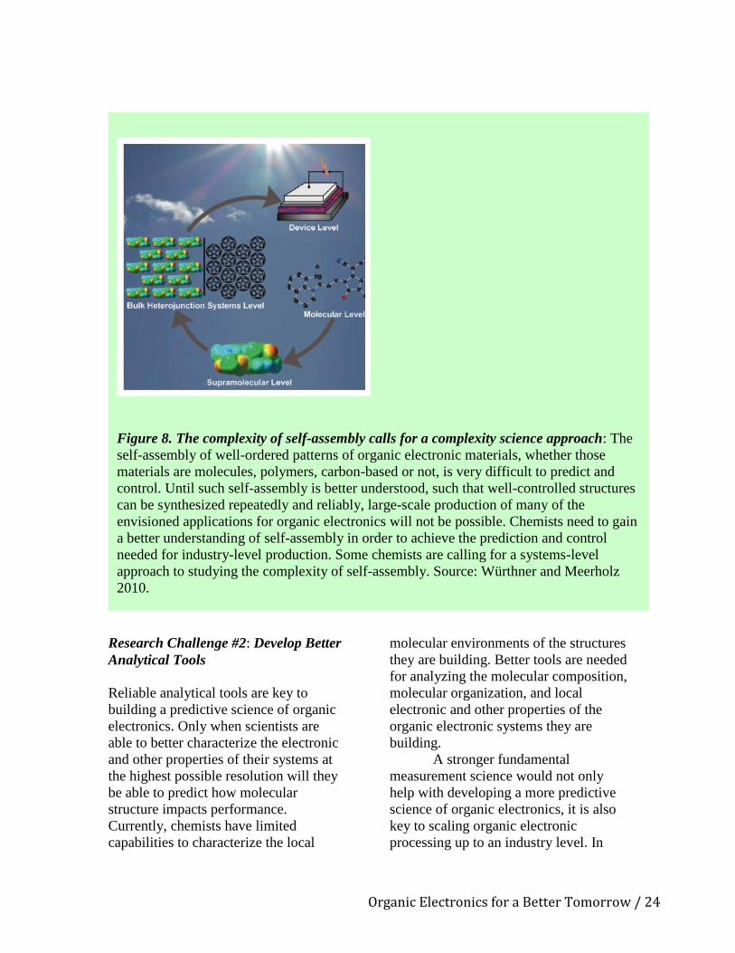
Figure 8. The complexity of self-assembly calls for a complexity science approach: The
self-assembly of well-ordered patterns of organic electronic materials, whether those
materials are molecules, polymers, carbon-based or not, is very difficult to predict and
control. Until such self-assembly is better understood, such that well-controlled structures
can be synthesized repeatedly and reliably, large-scale production of many of the
envisioned applications for organic electronics will not be possible. Chemists need to gain
a better understanding of self-assembly in order to achieve the prediction and control
needed for industry-level production. Some chemists are calling for a systems-level
approach to studying the complexity of self-assembly. Source: Würthner and Meerholz
2010.

Organic Electronics for a Better Tomorrow / 25
order to guarantee quality control,
process engineers need to know what is
happening at every point in the process.
They need non-invasive, non-
destructive, high-speed analytical tools.
Research Challenge #3: Improve
Three-Dimensional (3D) Processing
Technology
In order to scale organic electronic
processing up to an industry-level
standard, chemical scientists and
engineers need improved three-
dimensional (3D) fabrication
technologies. An important advantage of
many organic electronic structures and
devices is that they can be assembled on
plastic, paper and other flexible
substrates using existing low-cost, high-
throughput inkjet printing technologies.
Printing also enables large-area
fabrication of OLEDs, organic solar
cells, OFETs and other organic
electronic devices. Moreover, its
additive approach makes for more
sustainable production (i.e., necessary
resources are added as needed rather
than excess resources being subtracted
and removed as waste). However,
defect-free 3D processing of organic
electronic structures remains a major
challenge to industry-scale manufacture.
Engineers need to build on what has
already been done with 2D lithography
so that they can fabricate uniform 3D
structures in a controlled manner on a
nano-level, not just micron-level, scale.
Research Challenge #4: Increase
Multi-Functionality of Organic
Electronic Devices
Organic electronic devices can do more
than transport electronic information.
They can also transport optical,
magnetic, and thermal information.
Indeed, many of the organic electronic
devices already on the market are multi-
functional. For example, organic light-
emitting diodes (OLEDs) and organic
solar cells are multi-functional
optoelectronic devices, that is, electronic
devices that use or produce light in
addition to using or producing electrons.
As chemists gain better control over the
synthesis of organic materials, they and
their engineering collaborators will be
able to build increasingly sophisticated
optoelectronic and other multi-tasking
devices with multiple inputs and
multiple outputs. For example,
researchers envision multi-tasking
window glazings that function as solar
cells that generate electricity and as
OLEDs that generate light. In order to
fully realize the multifunctional capacity
of organic electronics, chemists need to
broaden their research focus beyond
charge transport and gain a better
understanding of how molecular
structure and interfacial behavior
impacts not just electronic but also
optical, magnetic, thermal and other
properties.

Organic Electronics for a Better Tomorrow / 26
CONCLUSION
In 2004, it was predicted that chemists
would soon synthesize organic
semiconductors with charge-carrier
mobilities greater than 10 cm2/Vs and
organic photovoltaic cells with 10
percent power conversion efficiencies.
Those predictions have come true. More
recently, it was predicted that organic
electronics would become a US$30
billion industry by 2015. While this
more recent prediction may have been
overly optimistic, nonetheless the field
of organic electronics clearly has made
tremendous strides over the past few
decades, with some devices already on
the market and a multitude of device
prototypes in development.
The field will continue to grow,
changing the way society interacts with
technology, as chemists, physicists, and
other scientists and engineers address the
research challenges identified by the
2012 CS3 symposium participants.
Multidisciplinary research and training
programs that bring together scientists
and engineers from different fields of
knowledge, as well as from different
sectors of activity (i.e., academia,
industry, government), will facilitate the
collaborative effort needed to meet these
challenges.

Organic Electronics for a Better Tomorrow / 27
REFERENCES
Abidian MR, Ludwig KA, Marzullo TC,
et al. 2009. Interfacing conducting
polymer nanotubes with the central
nervous system: chronic neural
recording using poly(3,4-
ethylenedioxythiophene) nanotubes.
Advanced Materials 21(37):3764-3770.
Bachilo SM, Strano MS, Kittrell C, et al.
2002. Structure-assigned optical spectra
of single-walled carbon nanotubes.
Science 298: 2361-2366.
Berrouard P, Najari A, Pron A, et al.
2012. Synthesis of 5-Alkyl[3,4-
c]thienopyrrole-4,6-dione-based
polymers by direct heteroarylation.
Angewandte Chemie International
Edition 52:2068-2072.
Briseno AL, Aizenberg J, Han YJ, et al.
2005. Patterned growth of large oriented
Organic semiconductor single crystals
on self-assembled monolayer templates.
Journal of the American Chemical
Society 127:12164-12165,
Cai J, Ruffieux P, Jaafar R, et al. 2010.
Atomically precise bottom-up
fabrication of graphene nanoribbons.
Nature 466(7305):470-473.
Chen W, Widawsky JR, Vazquez H, et
-
conjugated molecular junctions
covalently bonded to gold electrodes.
Journal of the American Chemical
Society 133:17160-17163.
Claussen JC, Franklin AD, ul Haque A,
et al. 2009. Electrochemical biosensor of
nanocube-augmented carbon nanotube
networks. ACS Nano 3(1):37-44.
Diez-Perez I, Hihath J, Lee Y, et. al.
2009. Rectification and stability of a
single molecular diode with controlled
orientation. Nature Communications 1:
635-641.
Drain CM, Nifiatis F, Vasenko A,
Batteas JD. Porphyrin tessellation by
design: metal mediated self-assembly of
large arrays and tapes. Angewandte
Chemie International Edition 37:2344-
2347.
Gabor NM, Zhong Z, Bosnick K, et al.
2009. Extremely efficient multiple
electron-hole pair generation in carbon
nanotube photodiodes. Science
325:1367-1371.
Gather MC, Köhnen A, Falcou A, et al.
2007. Solution-processed full-color
polymer OLED display fabricated by
direct photolithography. Advanced
Functional Materials 17: 191-200
Gather MC, Meerholz K, Danz N,
Leosson K. 2010. Net optical gain in a
plasmonic waveguide embedded in a
fluorescent polymer. Nature Photonics 4:
457-461.
Geim AK, Novoselov KS. 2007. The
rise of graphene. Nature Materials
6:183-191.
Haigh SJ, Gholinia A, Jalil R, et al.
2012. Cross-sectional imaging of
individual layers and buried interfaces of
graphene-based heterostructures and
superlattices. Nature Materials 11:764-
767.

Organic Electronics for a Better Tomorrow / 28
Hau, SK, Yip H-L, Acton O, et al. 2008.
Interfacial modification to improve
inverted polymer solar cells. Journal of
Materials Chemistry 18:5113-5119.
He Z, Zhong C, Hunag X, et al. 2011.
Simultaneous enhancement of open-
circuit voltage, short-circuit current
density, and fill factor in polymer solar
cells. Advanced Materials 23:4636-
4643.
Hodge SA, Bayazit MK, Coleman KS,
Shaffer MS. 2012. Unweaving the
rainbow: a review of the relationship
between single-walled carbon nanotube
molecular structures and their chemical
reactivity. Chemical Society Reviews
41(12):4409-4429.
Hoeben FJM, Jonkheijm P, Meijer EW,
Schenning APHJ. 2005. About
supramolecular assemblies of π-
conjugated systems. Chemical Reviews
105: 1491-1546
Ju S-Y, Doll J, Sharma I,
Papadimitrakopoulos F. 2008. Selection
of carbon nanotubes with specific
chiralities using helical assemblies of
flavin mononucleotide. Nature
Nanotechnology 3:356-362.
Kagan CR, Breen, TL, Kosbar, LL.
2001. Patterning organic-inorganic thin-
film transistors using microcontact
printed templates. Applied Physics
Letters 79:3536-3538.
Kaltenbrunner M, White MS, Glowacki
ED, et al. 2012. Ultrathin and
lightweight organic solar cells with high
flexibility. Nature Communications
3:Article number 770.
Kanibolotsky AL, Perepichka IF,
Skabara PJ. 2010. Star-shaped -
conjugated oligomers and their
applications in organic electronics and
photonics. Chemical Society Reviews
39:2695-2728.
Kim JB, Allen K, Oh SJ, et al. 2010.
Small-molecule thiophene-C60 dyads as
compatibilizers in inverted polymer solar
cells. Chemistry of Materials 22:5762-
5773.
Kim JB, Kim P, Pegard NC, et al. 2012.
Wrinkles and deep folds as photonic
structures in photovoltaics. Nature
Photonics 6:327-332.
Klauk H, Zschieschang U, Pflaum J,
Halik M. 2007. Ultralow-power organic
complementary circuits. Nature
4455:745-748.
Kohn PP, Huettner SS, Komber HH et
al. 2012. On the role of single
regiodefects and polydispersity in
regioregular poly(3-hexylthiophene):
defect distribution, synthesis of defect-
free chains, and a simple model for the
determination of crystallinity. Journal of
the American Chemical Society
134:4790-805.
Kuribara K, Wang H, Uchiyama N, et al.
2012. Organic transistors with high
thermal stability for medical
applications. Nature Communications
3:Article Number 723.
Levendorf MP, Kim C-J, Brown B, et al.
2012. Graphene and boron nitride lateral
heterostructures for atomically thin
circuitry. Nature 488:627-632.
Li G, Shrotriya V, Huang J, et al. 2005.
High-efficiency solution processable

Organic Electronics for a Better Tomorrow / 29
polymer photovoltaic cells by self-
organization of polymer blends. Nature
Materials 4:864-868.
Li N, Z Chen, W Ren, F Li, H Cheng.
2012. Flexible graphene-based lithium
ion batteries with ultrafast charge and
discharge rates. Proceedings of the
National Academy of Sciences
109(43):17360-17365.
Li Y, Sonar P, Singh SP, et al. 2011.
Annealing-free high-mobility
diketopyrrolopyrrole-quaterthiophene
copolymer for solution-processed
organic thin film transistors. Journal of
the American Chemical Society 133:
2198-2204.
Lv W, Tang D-M, He Y-B, et al. 2009.
Low-temperature exfoliated graphemes:
vacuum-promoted exfoliation and
electrochemical energy storage. ACS
Nano 3(11): 3730-3736
McCulloch I, Heeney M, Bailey C, et al.
2006. Liquid-crystalline semiconducting
polymers with high charge-carrier
mobility. Nature Materials 5:328-333.
Müller CD, Falcou A, Reckefuss N, et
al. 2003. Multi-color organic light-
emitting displays by solution processing.
Nature 421: 829-833.
Novoselov KS, Falko VI, Colombo PR.
2012. A roadmap for graphene. Nature
490:192-200.
Novoselov KS, Geim AK, Morozov SV,
et al. 2004. Electric field effect in
atomically thin carbon films. Science
306:666-669
Park SH, Roy A, Beaupre S, et al. 2009.
Bulk heterojunction solar cells with
internal quantum efficiency approaching
100 %. Nature Photonics 3:297-302.
Peet J, Kim JY, Coates E, et al. 2007.
Efficiency enhancement in low-bandgap
polymer solar cells by processing with
alkane dithiols. Nature Materials 6:497-
500.
Safont-Sempere MM, Fernández G,
Würthner F 2011. Self-sorting
phenomena in complex supramolecular
systems. Chemical Reviews 111: 5784-
5814.
Saudari SR, Frail PR, Kagan CR.
Ambipolar transport in solution-
deposited pentacene transistors enhanced
by molecular engineering of device
contacts. Applied Physics Letters
95:023301-023303.
Sekitani T, Noguchi Y, Hata K, et al.
2008. A rubberlike stretchable active
matrix using elastic conductors. Science
321(5895):1468-1472.
Sekitani T, Zschieschang U, Klauk H,
Someya T. 2010. Flexible organic
transistors and circuits with extreme
bending stability. Nature Materials
9:1015-1002.
Sirringhaus H, Brown PJ, Friend RH, et
al. 1999. Two-dimensional charge
transport in self-organized high-mobility
conjugated polymers. Nature 401:685-
688.
Sokolov AN, Tee BC, Bettinger CJ, et
al. 2012. Chemical and engineering
approaches to enable organic field-effect
transistors for electronic skin
applications. Accounts of Chemical
Research 45(3):361-71.

Organic Electronics for a Better Tomorrow / 30
Sun D, Timmermans MY, Tian Y, et al.
2011. Flexible high-performance carbon
nanotube integrated circuits. Nature
Nanotechnology 6:156-161.
Torrisi F, Hasan T, Wu W, et al. 2012.
Inkjet-printed graphene electronics. ACS
Nano 6:2992-3006.
United Nations [UN] System Task Team
on the Post-2015 UN Development
Agenda. Realizing the Future We Want
for All. Report to the Secretary-General.
https://docs.google.com/gview?url=http:
//sustainabledevelopment.un.org/content/
documents/614Post_2015_UNTTreport.
pdf&embedded=true.
Uwe H, Bunz F, Menning S, Martin N.
2012. Para-connected cyclophenylenes
and hemispherical polyarenes: building
blocks for single-walled carbon
nanotubes? Angewandte Chemie,
International Edition 51:2–10.
Wang QH, Hersam MC. 2009. Room-
temperature molecular-resolution
characterization of self-assembled
organic monolayers on epitaxial
graphene. Nature Chemistry 1: 206-211.
Woll A, Mukherjee MP, Levendorf EL,
et al. 2011. Oriented 2D covalent
organic framework thin films on single-
layer graphene. Science 332:228-231
Würthner F, Meerholz K. 2010. Systems
chemistry approach in organic
photovoltaics. Chemistry: A European
Journal. 16(31):9366-9373
Würthner F., Stolte M. 2011.
Naphthalene and perylene diimides for
organic transistors, Chemical
Communications 2011, 47, 5109-5115.
Xu B, Tao NJ. 2003. Measurement of
single-molecule resistance by repeated
formation of molecular junctions.
Science 301:1221-1223.
Yoo JE, Lee KS, Garcia A, et al. 2010.
Directly patternable, highly conducting
polymers for broad applications in
organic electronics. Proceedings of the
National Academy of Sciences
107:5712-5717.
Yoon M-H, Fachetti A, Marks TJ. 2005.
for low-voltage organic thin-film
transistors. Proceedings of the National
Academy of Sciences 102:4678-4682.
Zschieschang U, Yamamoto T,
Takimiya K, et al. 2011. Organic
electronics on banknotes. Advanced
Materials 23(5):654-658.

Organic Electronics for a Better Tomorrow / 31
2012 CS3 Participants
Name Institution Title
China Delegation
Xi Zhang (Chair) Tsinghua University,
Beijing
Professor of Chemistry
He Tian East China University of
Science and Technology,
Shanghai
Professor of Chemistry and
Molecular Engineering
Lixiang Wang Chinese Academy of
Sciences, Changchun
Professor, Changchun
Institute of Applied
Chemistry
Jian Pei Peking University, Beijing Professor of Chemistry
Jin Zhang Peking University, Beijing Professor of Chemistry
Zhigang Shuai (liaison) Tsinghua University,
Beijing
Professor Chemistry
Yunqui Liu Chinese Academy of
Sciences, Beijing
Germany Delegation
Peter Bäuerle (chair) Ulm University, Ulm Director, Institute of
Organic Chemistry II and
Advanced Materials
Frank Würthner University Würzburg,
Würzburg
Professor, Institute of
Organic Chemistry
Klaus Meerholz University of Cologne,
Cologne
Professor, Institute of
Physical Chemistry
Stefan Hecht Humboldt-Universität zu
Berlin, Berlin
Professor, Laboratory of
Organic Chemistry and
Functional Materials,
Department of Chemistry
Andreas Hirsch University Erlangen-
Nuremberg, Erlangen
Professor/Chair, Organic
Chemistry
Horst Hahn Karlsruhe Institute of
Technology, Eggenstein-
Leopoldshafen
Executive Director
Hans-Georg Weinig
(liaison)
German Chemical Society Head Education and
Science

Organic Electronics for a Better Tomorrow / 32
Markus Behnke German Research
Foundation (DFG)
Program Director
Japan Delegation
Takuzo Aida (chair) University of Tokyo,
Tokyo
Professor, Departments of
Chemistry and
Biotechnology, School of
Engineering
Yoshiharu Sato Mitsubishi Chemical
Group Science and
Technology Research
Center, Inc., Tokyo
Senior Researcher,
Photovoltaics Project
Mitsuo Sawamoto Graduate School of
Engineering, Kyoto
University, Kyoto
Professor, Department of
Polymer Chemistry
Takao Someya School of Engineering,
University of Tokyo,
Tokyo
Professor, Department of
Electrical Engineering
Kazuo Takimiya Graduate School of
Engineering, Hiroshima
University, Higashi-
Hiroshima
Professor, Department of
Applied Chemistry
Masahiro Yamashita Graduate School of
Science, Tohoku
University, Sendai, Miyagi
Professor, Department of
Chemistry
Nobuyuki Kawashima
(liaison)
Chemical Society of Japan,
Tokyo
Executive Director and
Secretary General
Mitsuhiko Shionoya Japan Society for the
Promotion of Science
(JSPS), Tokyo
Graduate School of
Science, University of
Tokyo
United Kingdom Delegation
Peter Skabara (chair) University of Strathclyde,
Glasgow, Scotland
Professor of Materials
Chemistry
Stephen Yeates University of Manchester,
Manchester, England
Professor of Polymer
Chemistry
Karl Coleman Durham University,
Durham, England
Reader, Department of
Chemistry
Martin Heaney Imperial College London,
London, England
Reader of Materials
Chemistry, Department of
Chemistry

Organic Electronics for a Better Tomorrow / 33
Andrew Monkman Durham University,
Durham, England
Director, Photonic
Materials Centre,
Department of Physics
Richard Walker (liaison) Royal Society of
Chemistry, Cambridge,
England
Science Executive
Clare Bumphrey Engineering and Physical
Sciences Research Council,
Swindon, England
Physical Sciences Portfolio
Manager
United States Delegation
Cherie Kagan (chair) University of
Pennsylvania, Philadelphia,
Penn.
Professor, Departments of
Chemistry, Electrical and
Systems Engineering, and
Materials Science and
Engineering
Lynn Loo Princeton University,
Princeton, New Jersey
Professor, Department of
Chemical and Biological
Engineering
Claudia Arias University of California,
Berkeley
Acting Associate
Professor, Department of
Electrical Engineering and
Computer Sciences
Colin Nuckolls Columbia University, New
York, New York
Professor, Department of
Chemistry
James Batteas Texas A&M University,
College Station, Texas
Professor, Department of
Chemistry
Jiwoong Park Cornell University, Ithaca,
New York
Asst. Professor,
Department of Chemistry
and Chemical Biology
Dat Tran (liaison) American Chemical
Society, Washington, D.C.
International Activities
Manager, Office of
International Activities
Francisco Gomez American Chemical
Society, Washington, D.C.
Assistant Director, Office
of International Activities
Zeev Rosenzweig National Science
Foundation, Arlington,
Virginia
Program Director
Leslie Pray (science writer) Independent Consultant,
Los Angeles, California