OPTOELECTRONIC MODULATORS FOR OPTICAL …web.stanford.edu/group/dabmgroup/publications/t12.pdf ·...
141
OPTOELECTRONIC MODULATORS FOR OPTICAL INTERCONNECTS A DISSERTATION SUBMITTED TO THE DEPARTMENT OF APPLIED PHYSICS AND THE COMMITTEE ON GRADUATE STUDIES OF STANFORD UNIVERSITY IN PARTIAL FULFILLMENT OF THE REQUIREMENTS FOR THE DEGREE OF DOCTOR OF PHILOSOPHY Noah Charles Helman May 2005
-
Upload
nguyenthuan -
Category
Documents
-
view
221 -
download
0
Transcript of OPTOELECTRONIC MODULATORS FOR OPTICAL …web.stanford.edu/group/dabmgroup/publications/t12.pdf ·...

OPTOELECTRONIC MODULATORS
FOR OPTICAL INTERCONNECTS
A DISSERTATION
SUBMITTED TO THE DEPARTMENT OF APPLIED PHYSICS
AND THE COMMITTEE ON GRADUATE STUDIES
OF STANFORD UNIVERSITY
IN PARTIAL FULFILLMENT OF THE REQUIREMENTS
FOR THE DEGREE OF
DOCTOR OF PHILOSOPHY
Noah Charles Helman
May 2005

ii
© Copyright by Noah Helman 2005
All Rights Reserved

iii
I certify that I have read this dissertation and that, in my opinion, it is fully adequate in scope and quality as a dissertation for the degree of Doctor of Philosophy.
____________________________________
David A. B. Miller, Principal Advisor
I certify that I have read this dissertation and that, in my opinion, it is fully adequate in scope and quality as a dissertation for the degree of Doctor of Philosophy.
____________________________________
Martin M. Fejer
I certify that I have read this dissertation and that, in my opinion, it is fully adequate in scope and quality as a dissertation for the degree of Doctor of Philosophy.
____________________________________
Olav Solgaard
Approved for the University Committee on Graduate Studies:
____________________________________
iv
Abstract
Optical interconnects have been widely studied as a solution to the electrical
interconnect bottleneck foreseen in computing systems. The mature technology of silicon
CMOS electronics is well-established for high-speed information processing, while optical
systems excel at information transmission. Future computing systems are likely to
incorporate electronic components communicating along an optical channel that requires
optoelectronic devices to convert signals from the electronic into the optical domain and
vice versa.
Electroabsorption modulators designed for this application must be compatible
with both the electrical and optical systems. This dissertation will begin with a
discussion of the requirements for an optoelectronic modulator design. In particular, I
will describe the advantages and challenges of 2D arrays of surface-normal modulators
that operate over a wide wavelength range with a low voltage drive.
Two surface-normal modulator architectures will be presented. First, I will
outline the design, fabrication and integration of an asymmetric Fabry-Perot
AlGaAs/GaAs modulator. Following a post-integration cavity tuning step, this device
achieved a contrast ratio of 3 dB over a wavelength range from 847 nm to 852 nm using a
voltage drive of only 1 V. The second device, a novel design called the quasi-waveguide
angled-facet electroabsorption modulator (QWAFEM), was simulated and fabricated in
the InGaAsP/InP material system. An experimental contrast ratio of 3 dB over a 16 nm
wavelength range near 1510 nm was measured for a voltage drive of only 0.8 V. To the
best of our knowledge, no other reported low-voltage surface-normal modulator offers 3
dB of contrast ratio over such a wide wavelength range around 1.5 µm. Improvements to
the QWAFEM design were simulated and a brief discussion of the advantages and
practical challenges of such devices precedes the conclusion.
v
Acknowledgements At the end of my first year of college, I visited a professor, Bob Woollacott, who
had befriended me, to seek out his advice about summer school. My first year had me so
excited; I wanted to just keep taking more and more courses. But I was worried that the
professors who taught the summer courses might not be the same as those that taught the
term-time courses. I distinctly remember his response. “The faculty are the same as
during the term,” he said, “but I still don’t recommend that you take summer courses.
Most of the students are still in high school; they’re not yet undergrads… You do realize
you learn mostly from your peers, and not from the professors, right?”
Since then I have been quite aware of how much I have learned from my peers.
(As an aside, I later became a summer school lecturer and remarked on the irony of the
story.) I have been so fortunate in both my undergraduate studies and my graduate career
to have been surrounded by such wonderful people.
First of all and most importantly, I need to thank Sameer Bhalotra, my closest
friend, co-worker, co-conspirator, and consigliere over the last eleven years. It would be
nearly impossible to explain in a few short sentences how Sameer has influenced me. I
have learned so much from him in almost all areas of thinking (physics, math,
engineering, philosophy, psychology, music, strategy, sports, etc.) and he has always
encouraged my curiosity by seriously considering any question. I cannot imagine the
person I would be if I had not met him and I cannot thank him enough for being the
qwertiest dude I know. I can only hope that The Lexington Project is successful.
My closest co-workers at Stanford have also been highly influential in my life.
Gordon Keeler and I worked together on all of the AlGaAs modulator research (and
more) and I must thank him for taking me under his wing. I relied on Gordon’s
leadership, scientific skill and expertise for the first three years I was in graduate school,
and when he graduated, I was a little frightened that I might not do so well without him
around. He was a fantastic mentor, always positive and fun to work with. We managed
to have fun, even under the most frustrating conditions (e.g. clean-room failures).
During the QWAFEM research project, I was fortunate enough to work with
Hatice Altug, Jon Roth, and Dave Bour. I greatly appreciate the work Hatice put into the

vi
initial design of the optical test setup as well as the hours she logged in the clean-room
with me. Jon picked up where she left off and added significantly to the project both in
the computer simulations and in the clean-room as well. He has always been eager to
learn and I appreciate all his help. I hope that I was anywhere near the mentor to them
that Gordon was to me. Dave Bour at Agilent Labs grew several samples for us, but his
involvement in the project was greater than that. He has always been more than eager to
help us, to learn about what we are working on, and to connect us to people who might be
able to answer our questions.
The other members of the Miller Group were always fun and extremely helpful.
The lab environment was so friendly – all the students would jump to help you answer a
question. I would like to thank all of them – Micah, Diwakar, Christof, Helen, Vijit,
Volkan, Petar, Rafael, Martina, Gordon, Bianca, Ryohei, Sameer, Yang, Aparna, Henry,
Ray, Onur, Mike, Jon, Luke, Ekin, Salman, and Shen – as well as our collaborators in the
Harris Group – Rafael, Mark, Thierry, Chien-Chung, Seth, and Vince – and Horowitz
Group – Sam and Azita.
My research advisor, Prof. David Miller, has been a fantastic person to get to
know. I feel that I have learned from him not only physics theories and experimental
techniques, but also scientific curiosity, integrity, and persistence. The term “advisor”
properly describes his role with the students – I have appreciated his advice, as well as
his sense of humor, in many different areas of life over our many conversations. His
ability to manage the lab, motivating all the students to creatively solve problems while
having to focus a lot of his attention on funding, administrative issues, teaching, and
writing textbooks, is something that I hope to emulate some day as a faculty member
myself.
Prof. Marty Fejer and Prof. Olav Solgaard kindly read my entire thesis, made
constructive suggestions, and participated with Prof. Jim Harris and Prof. Jim Ferrell on
my Ph.D. Orals Committee and I am indebted to them all. Prof. Solgaard arrived as a
professor at Stanford during my first year here, and he has always been generous with his
time, supportive and quick-witted.
I received technical help from several folks that I would like to thank. First, Tom
Carver, who runs the Ginzton Microfabrication Facility, has been an endless source of

vii
useful knowledge regarding the details of semiconductor processing. Without his help, I
would have reinvented a hundred wheels. Second, Tim Brand, who runs the Ginzton
Crystal Shop, seems to be able to accomplish anything and I want to thank him in
particular for many enjoyable non-science conversations. Ning Cao at UCSB’s
fabrication facility performed a useful etching step in our QWAFEM process and I must
thank him for his effort.
The administration of Ginzton and the Applied Physics Department is handled
ably by many people who always stopped what they were doing to help me solve my
problems. In particular, I would like to thank Ingrid Tarien, Paula Perron, and Claire
Nicholas for looking out for me in the vast bureaucratic sea of Stanford. The financial
support for this work came from a Gerhard Casper Stanford Graduate Fellowship as well
as the MARCO forum (through the Interconnect Focus Center and DARPA).
Finally, I would like to thank all the friends and family who have supported me
and made me laugh during the last six years. My move to California has always been a
double-edged sword for me – with my family in Boston and many friends all over, it was
difficult to be so far away from everyone. Fortunately, I had a large group of friends who
moved out to the Bay Area at about the same time and I can say we’ve had a great time.
In particular, I would like to thank the members of the IDDD, as well as my Framingham
posse, some old Harvard friends, and all the great folks I’ve met at Stanford and
Berkeley. My four parents, six grandparents and many siblings have always encouraged
me to study whatever interested me. Aside from casually asking when I planned to move
back east, they have all uniformly supported all my decisions. And then there’s Rachel.
On those inevitable days when I thought this project might never work, she put her arm
around me and told me it would. Rachel, you are the best partner, the silliest girl I know,
the most fun, the one who makes me laugh the most, the one who challenges me, the one
who sparked my social consciousness, and the one who inspires me to be better than I am
in all ways.
I cannot thank you all enough. I am at this point because of all of you.

viii
Table of Contents List of Tables xii
List of Illustrations xiii
Chapter 1: Introduction 1
References 4
Chapter 2: Optical Interconnects 5
2.1 Electrical Interconnects 5
2.1.1 Frequency-dependent loss 6
2.1.2 Impedance mismatching 7
2.1.3 Cross-talk 7
2.1.4 Advanced electrical interconnect schemes 8
2.1.5 Advantages of electrical interconnects 8
2.2 Optical Interconnects 9
2.2.1 Frequency-dependent loss 9
2.2.2 Impedance mismatching 9
2.2.3 Interconnect density 10
2.2.4 Cross-talk 10
2.2.5 Wavelength-division multiplexing 10
2.2.6 Challenges for practical optical interconnects 11
2.3 Current Practical Demonstrations of Optical Interconnects 12
2.3.1 Industrial optical interconnects efforts 12
2.3.2 Academic optical interconnects groups 13
2.4 Summary 16
References 17
Chapter 3: Transmitter Devices for Optical Interconnects 20
3.1 Device Requirements for Optical Interconnect Transmitters 20
3.1.1 Electrical requirements 20

ix
3.1.1.1 Digital voltage level 21
3.1.1.2 Off-chip single-channel data rate 21
3.1.1.3 Power consumption 22
3.1.2 Optical requirements 23
3.1.2.1 Operating wavelength band 23
3.1.2.2 Contrast ratio and insertion loss 23
3.1.2.3 2D arrays of devices 24
3.1.2.4 Optical bandwidth/wavelength range 25
3.1.3 System integration 25
3.1.3.1 Integration of optoelectronics and electronics 25
3.1.3.2 Integration of optical system with optoelectronic chips 26
3.1.4 Summary of optoelectronic transmitter requirements 27
3.2 Comparison of VCSELs and Modulators 27
3.2.1 VCSELs 27
3.2.2 Modulators 29
3.2.2.1 Description of how modulators work 29
3.2.2.2 Semiconductor electroabsorption modulators: waveguides 30
3.2.2.3 Semiconductor electroabsorption modulators: surface-normal 30
References 34
Chapter 4: AlGaAs MQW Surface-Normal Modulators 38
4.1 Basics 38
4.2 Design 39
4.3 Fabrication and Integration 40
4.4 Asymmetric Fabry-Perot Modulators 45
4.5 AFPM Theoretical Treatment 46
4.6 Transfer Matrix Method Modeling 47
4.7 Experimental Technique of Cavity Tuning 48
4.8 Systems Experiments Using AlGaAs Modulators 52
4.9 Summary 53
References 54

x
Chapter 5: Quasi-Waveguide Angled-Facet Electroabsorption Modulator 57
5.1 Introduction 57
5.1.1 Low-voltage operation 57
5.1.2 Compatibility with larger optical networks 59
5.1.3 Summary of requirements 60
5.2 Previous Work on 1550 nm Surface-Normal Modulators 60
5.3 QWAFEM: An Introduction 61
5.3.1 Description and advantages of QWAFEM 61
5.3.2 Misalignment tolerance 62
5.3.3 Large incident angle 63
5.4 Angle Propagation AFPM and Simulations 65
5.5 Optimization Technique 71
5.6 Wafer Growth Variations 73
5.7 Wafer Growth and Testing 73
5.8 Fabrication 74
5.8.1 Mesa etch and n-contacts 74
5.8.2 Etching angled mirrors 75
5.8.2.1 Ti-mask angled mirror procedure 75
5.8.2.1 InGaAsP angled mirror procedure 75
5.8.3 Flip-chip bonding 79
5.9 Experimental Results 80
5.9.1 Reflectivity and contrast ratio 81
5.9.2 Misalignment tolerance 83
5.9.3 Capacitance, speed, and power dissipation 84
5.9.4 Insertion loss 85
5.9.5 Angular acceptance 85
5.10 Drawbacks of QWAFEM 87
5.11 Summary 89
References 90

xi
Chapter 6: Improvements and Future Directions 92
6.1 Quantum Well Design 92
6.2 Frustrated TIR QWAFEM 93
6.2.1 Concept and simulations 93
6.2.2 Fabrication methods for frustrated TIR QWAFEM 94
6.2.3 Advantages 95
6.3 GaInNAs(Sb) QWAFEM 95
6.4 LUCSEL 97
6.5 Systems Using QWAFEMs 98
6.6 Summary 100
References 101
Chapter 7: Conclusions 102
Appendix A: Lithography Procedure and Fabrication Instructions for
AlGaAs/GaAs Modulators 104
Appendix B: MATLAB Simulation Code for QWAFEM 113
Appendix C: QWAFEM Fabrication Instructions 124

xii
List of Tables
Chapter 4
Table 4.1 Contrast ratio and change in reflectivity for several voltages 52
Chapter 5
Table 5.1 Comparison between previously reported 1550-nm surface-normal modulators and QWAFEM 83

xiii
List of Illustrations
Chapter 2
Figure 2.1 Planar optics of Jahns and Gruber 15
Chapter 3
Figure 3.1 QCSE of AlGaAs/GaAs quantum wells 30
Figure 3.2 Schematic of reflection-mode surface-normal modulator 32
Chapter 4
Figure 4.1 Schematic of AlGaAs modulator flip-chip bonded to CMOS 38
Figure 4.2 Wafer design for AlGaAs modulators 39
Figure 4.3 Schematic of fabrication steps before flip-chip bonding 40
Figure 4.4 Scanning electron micrograph of devices before bonding 41
Figure 4.5 Schematic of flip-chip bonding and substrate removal 42
Figure 4.6 SEM of finished modulators flip-chip bonded to CMOS 43
Figure 4.7 Array of AlGaAs modulators in forward bias 43
Figure 4.8 Reflectivity of modulators vs. wavelength at different reverse biases 44
Figure 4.9 Schematic of AFPM version of the AlGaAs modulator 46
Figure 4.10 Field diagram for AFPM equations 46
Figure 4.11 Cavity tuning results in shifting the Fabry-Perot resonance 50
Figure 4.12 Simulation and experiment of AFPM AlGaAs modulators 51
Figure 4.13 Contrast ratio and reflectivity change for AFPM modulators 51
Chapter 5
Figure 5.1 AFPM simulation for two cavity thicknesses: reflectivity vs. wavelength 58
Figure 5.2 QCSE for InGaAsP MQW region grown on InP 59
xiv
Figure 5.3 QWAFEM schematic 61
Figure 5.4 Misalignment tolerance geometry of QWAFEM 63
Figure 5.5 Geometry of ray optics factor of 1/cos(θ) 63
Figure 5.6 Power reflectivity vs. incident angle for a single interface of InP and InGaAsP 64
Figure 5.7 Absorption coefficient vs. wavelength for three values of the applied electric field 66
Figure 5.8 Simulated optical intensity in various structures 67
Figure 5.9 Angular resonance as a function of the number of DBR pairs 68
Figure 5.10 Angular resonance for 3-pair DBR for various beam waists 70
Figure 5.11 QWAFEM design before and after optimization 72
Figure 5.12 Simulation of optimized design using MQW data from previous runs 73
Figure 5.13 Microscope image (top-view) of three devices before V-grooves were etched 76
Figure 5.14 Microscope images of V-grooved sample (side- and top-view) 76
Figure 5.15 SEM of rough angled facets 77
Figure 5.16 SEM of smoothed angled facet 78
Figure 5.17 SEM of finished devices before flip-chip bonding 79
Figure 5.18 Probe station experimental setup 80
Figure 5.19 Reflectivity of QWAFEM for 0.8-V drive 81
Figure 5.20 Contrast ratio of QWAFEM for 0.8-V drive 82
Figure 5.21 Measurement of misalignment tolerance 83
Figure 5.22 Diagram of mesa structure and polishing 86
Figure 5.23 Angular acceptance of QWAFEM 87
Chapter 6
Figure 6.1 New quantum well types 92
Figure 6.2 Schematic of frustrated TIR QWAFEM wafer structure 93

xv
Figure 6.3 Simulated contrast ratio vs. wavelength for frustrated TIR QWAFEM design 94
Figure 6.4 GaInNAs(Sb) MQW QCSE data for 2 V and 6 V reverse bias 96
Figure 6.5 Simulated contrast ratio and change in reflectivity of GaInNAs(Sb) MQW in QWAFEM configuration using 1-V drive 97
Figure 6.6 LUCSEL schematic 98
Figure 6.7 Planar optics system, showing where arrays of QWAFEMs may be bonded in order to integrate the two technologies 100
1
CHAPTER 1 : INTRODUCTION
As computer technology improves, the information processing power increases
with each generation. Advances in design and fabrication of individual computer chips
enable devices to operate faster, to consume less electrical power, and to perform more
complex functions. Primarily, this is achieved by shrinking the size scale of the
transistors and using a lower voltage swing to denote the digital bits. Though this plan of
shrinking the transistor size is projected to continue to improve the performance of the
chips, the Semiconductor Industry Association has predicted that the performance of the
overall system in the upcoming years will be limited by the metallic wires that connect
the chips to each other [1]. Even though the processors and memory may get faster and
more efficient, the ability of these chips to communicate with each other will become
impaired by the imperfections of the electrical interconnections. Predictions of when
electrical interconnects will become the performance-limiting factor of computers vary
somewhat, but most predict the necessity of addressing the problem between 2009 and
2014 [1-3].
Several researchers have investigated these fundamental limits of electrical
interconnects and have proposed various solutions [2-16]. Perhaps, advanced electronic
architectures will be sufficient to address these problems for the upcoming future [15,
16]. In parallel to these all-electrical approaches, many research efforts have been
focused on replacing the wires with optical links. For fundamental physical reasons,
optical interconnects offer many advantages over electrical interconnects for high speed
links [4]. However, practical concerns, such as manufacturability, design complexity,
reliability, and cost, must also be taken into account in considering whether optical
interconnects will penetrate the marketplace [3].
The vision of optical interconnects consists of many powerful electronic
information processing modules communicating with each other and with the internet’s
optical network via optical channel links. This design would utilize the strengths of both
technologies: electronics for information processing and optics for communications.
Currently, optical networks for long-distance telecommunications (“long-haul”) are
widespread and carry most of the voice and data traffic. Demand for internet bandwidth

2
has increased at a steady rate in the last several years, despite fluctuations in the
economic markets [17]. The network providers have responded by installing optical
systems to replace wide-area and metro-area networks. This demand trend is likely to
continue, driving optical networks to shorter and shorter distances.
Electrical signals that are targeted for an off-chip destination in an optical-
interconnect system must be converted into the optical domain for transmission and then
back into an electrical signal at the receiver chip. Many devices have been proposed for
these electrical-to-optical (EO) and optical-to-electrical (OE) converters. The focus of
this dissertation is the design of semiconductor optoelectronic modulators optimized as
EO transmitter devices for optical interconnects.
Chapter 2 will address the advantages of optical interconnects over electrical
interconnects. Chapter 3 will outline the optoelectronic design requirements, device
architectures, and tradeoffs for this application. The focus of Chapter 4 will be an
AlGaAs-based surface-normal device that was designed, fabricated, and tested as both a
modulator (transmitter) and a photodetector (receiver). Next, an InGaAsP/InP quasi-
waveguide angled-facet electroabsorption modulator (QWAFEM) was investigated as a
high-speed modulator for use in practical optical interconnects systems. The factors that
were critical in the design, processing, and testing of that device will be presented in
Chapter 5. The results of these experiments enable us to model improvements in
performance while still meeting the various design constraints that we set out in Chapter
3. Some of these improvements are discussed in Chapter 6 before a brief summary and
conclusion in Chapter 7.
3
REFERENCES
[1] Semiconductor Industry Association, "International Technology Roadmap for Semiconductors," http://public.itrs.net/Files/2003ITRS/Home.htm, 2003.
[2] D. A. B. Miller, "Optical interconnects to silicon.," IEEE Journal of Selected Topics in Quantum Electronics, vol. 6, pp. 1312-17, 2000.
[3] D. A. B. Miller, "Rationale and challenges for optical interconnects to electronic chips.," Proceedings of the IEEE, vol. 88, pp. 728-49, 2000.
[4] D. A. B. Miller, "Physical reasons for optical interconnection.," International Journal of Optoelectronics, vol. 11, pp. 155-68, 1997.
[5] J. W. Goodman, F. J. Leonberger, S. Y. Kung, and R. A. Athale, "Optical interconnections for VLSI systems.," Proceedings of the IEEE, vol. 72, pp. 850-66, 1984.
[6] A. V. Krishnamoorthy and D. A. B. Miller, "Firehose architectures for free-space optically interconnected VLSI circuits.," Journal of Parallel and Distributed Computing, vol. 41, pp. 109-14, 1997.
[7] H. Thienpont, C. Debaes, V. Baukens, H. Ottevaere, P. Vynck, P. Tuteleers, G. Verschaffelt, B. Volckaerts, A. Hermanne, and M. Hanney, "Plastic microoptical interconnection modules for parallel free-space interand intra-MCM data communication.," Proceedings of the IEEE, vol. 88, pp. 769-79, 2000.
[8] X. Z. Zheng, P. J. Marchand, D. W. Huang, and S. C. Esener, "Free-space parallel multichip interconnection system.," Applied Optics, vol. 39, pp. 3516-24, 2000.
[9] G. Q. Li, D. W. Huang, E. Yuceturk, P. J. Marchand, S. C. Esener, V. H. Ozguz, and Y. Liu, "Three-dimensional optoelectronic stacked processor by use of free-space optical interconnection and three-dimensional VLSI chip stacks," Applied Optics, vol. 41, pp. 348-360, 2002.
[10] C. Debaes, M. Vervaeke, V. Baukens, H. Ottevaere, P. Vynck, P. Tuteleers, B. Volckaerts, W. Meeus, M. Brunfaut, J. Van Campenhout, A. Hermanne, and H. Thienpont, "Low-cost microoptical modules for MCM level optical interconnections.," IEEE Journal of Selected Topics in Quantum Electronics, vol. 9, pp. 518-30, 2003.
[11] N. M. Jokerst, M. A. Brooke, S. Y. Cho, S. Wilkinson, M. Vrazel, S. Fike, J. Tabler, Y. J. Joo, S. W. Seo, D. S. Wills, and A. Brown, "The heterogeneous integration of optical interconnections into integrated microsystems.," IEEE Journal of Selected Topics in Quantum Electronics, vol. 9, pp. 350-60, 2003.
[12] S. K. Lohokare, D. W. Prather, J. A. Cox, P. E. Sims, M. G. Mauk, and O. V. Sulima, "Integrated optoelectronic transmitter and receiver multi-chip modules for three-dimensional chip-level micro-optical interconnects," Optical Engineering, vol. 42, pp. 2683-2688, 2003.
[13] M. Gruber, "Multichip module with planar-integrated free-space optical vector-matrix-type interconnects.," Applied Optics, vol. 43, pp. 463-70, 2004.
[14] M. Gruber, R. Kerssenfischer, and J. Jahns, "Planar-integrated free-space optical fan-out module for MT-connected fiber ribbons.," Journal of Lightwave Technology, vol. 22, pp. 2218-22, 2004.

4
[15] J. D. Meindl, "Interconnect opportunities for gigascale integration.," IEEE Micro, vol. 23, pp. 28-35, 2003.
[16] R. H. Havemann and J. A. Hutchby, "High-performance interconnects: an integration overview.," Proceedings of the IEEE, vol. 89, pp. 586-601, 2001.
[17] Japan Internet Exchange Company , "Daily Traffic Across JPIX Backplane," http://www.jpix.ad.jp/en/techncal/traffic.html, 2004.

5
CHAPTER 2 : OPTICAL INTERCONNECTS
This chapter is devoted to looking at the advantages and disadvantages of
electrical and optical interconnects, from both fundamental physical arguments as well as
practical considerations. I argue that optical interconnects are likely to become necessary
for certain applications, such as internet-router backplanes and possibly personal
computers, at data rates that are expected to be reached by Si complementary metal-
oxide-semiconductor (CMOS) in the next 5-10 years (2010 – 2015). This intermediate
conclusion will motivate the rest of this dissertation – a detailed investigation into
semiconductor optoelectronic modulators as transmitter devices for optical interconnects.
2.1 ELECTRICAL INTERCONNECTS Current technology in CMOS electronics operates chip speeds up in the multi-
GHz clock rates and transistor gates down to 90 nm. Moore’s Law does not seem to be
slowing down in the near future, according to the ITRS Roadmap [1]. Yet, electrical
interconnects do not seem poised to keep up. Metal wires are currently being used to
connect chips to boards (links ~10-cm long), boards to boards (~50 cm), router linecards
to each other (~3 m) and so on. Unfortunately, at frequencies above about 5 GHz, a
copper wire along an internet router backplane fails to be a simple electrical signal
channel [2]. The many imperfections of the metallic interconnect, such as frequency-
dependent loss, impedance mismatching, and skin depth, complicate the transmitter
circuitry. To some extent, these problems can be overcome, at a cost of electrical power
consumption. Since the heat extraction from CMOS chips has recently become a serious
problem [1, 3], reducing electrical power consumption has developed into a high-priority
design issue.
In the following sections, we take a closer look at each of the major issues with
electrical interconnects.
6
2.1.1 FREQUENCY-DEPENDENT LOSS
Mohammed et al. at Intel [4] simulated a 20-inch electrical interconnect on a
standard printed circuit (PC) board using parameters for the material FR4. Their results
(shown in their Fig. 2) indicate that there is an insertion loss of about -25 dB at 5 GHz
and about -45 dB at 10 GHz. At higher signal frequencies, the loss in the electrical
interconnect gets even worse. Similar figures are shown in the Ph.D. dissertation of Dr.
Azita Emami-Neyestanak in Fig. 2.16 [2]. In absolute terms, this amount of loss is
severe, and the variation in loss with respect to frequency causes signal distortion.
A 10-Gigabit-per-second (Gbps) signal (non-return-to-zero, intensity modulated)
that must pass through this channel contains frequency components up to 5 GHz. These
various frequency components suffer a different amount of loss, resulting in a distorted
signal at the receiver. To some degree, a process called equalization can compensate for
this aspect of the channel by amplifying frequency components that are more strongly
attenuated during the transmission. Equalization, however, requires foreknowledge of
the data transfer rate and of the channel characteristics (or at least some active method of
determining the characteristics) and consumes valuable chip area and electrical power
[4]. As the bit rates increase, the loss of the electrical channel gets worse, and
equalization schemes will only become less practical.
A second consequence of the frequency-dependent loss of the electrical channel is
the so-called “aspect-ratio limit” of electrical lines [5, 6]. The capacity of an electrical
interconnect system is essentially limited by the aspect ratio of the wires (the cross-
sectional area divided by the length squared) used to extract the information. Since the
distance that must be traveled by the signal and the size of the chips are usually fixed in a
system, this aspect-ratio maximum can be calculated and thus, the maximum aggregate
data rate is known. In other words, it does not matter what specific architecture is
implemented (e.g. many small wires or a few large wires) – filling a particular volume
with information-carrying wires will result in the ability to transmit only a certain amount
of data per second. Advanced techniques such as multilevel coding and repeatering can
be used to extend this limit somewhat, but again these techniques consume additional
power [2].
7
2.1.2 IMPEDANCE MISMATCHING
Considering just board-to-board interconnects for a moment leads us to address
the problem of impedance mismatching. In a practical computer/router system, the
electronic boards are plugged into a backplane which connects the many boards to each
other. A signal generated on one board, for example, must pass through the ball grid
array on the transmitter chip onto the printed circuit board (PCB), travel along a metal
trace on the board to the edge, cross over to the backplane through a connector, along the
backplane, through another connector, along another board, and through another ball grid
array contact in order to arrive at the receiver circuit. At each interface, two traces come
together in a way that is likely to contain some discontinuities in the size and shape of the
joint between them. Electrical signals passing through such discontinuities generate
reflections due to the impedance mismatch at the interface [2, 7]. It is essential that these
reflections be minimized because they can cause intersymbol interference (ISI). ISI
means the information in one bit is corrupted somewhat by the energy or information in
some other bit(s) in the data stream. ISI, in this case, is essentially an ‘echo’ – the first
part of a signal tries to pass these interfaces, but some of the energy is reflected and when
it comes back in the same direction a split second later, this ‘echo’ gets superimposed
with the signal that is currently trying to pass the interface for the first time. Clearly, the
ability of the receiver to properly distinguish the original information in the signal will be
compromised somewhat by this echo, just as it is difficult to understand the speech of
someone who is standing in a strongly echoing environment, like a shower room. (Note
that reflections are not the only cause of ISI. Other channel imperfections, such as
dispersion, can lead to ISI as the energy from one bit corrupts the adjacent bits in time.
Regardless of its source, ISI should be minimized and it is significantly more problematic
in electronic channels than in optical channels, as we will see.)
2.1.3 CROSS-TALK
As the highest frequency in an electrical signal approaches 5-10 GHz, a wire with
an oscillating electric field at that frequency will be emitting radiation that will be picked
up by nearby wires. Thus, a signal that is supposed to be confined to one wire will
actually be contributing to the energy or signal carried on another wire. This “cross-talk”
8
is obviously noise on the receiving signal that degrades the ability of the receiver circuit
to properly distinguish the digital levels. The large amount of data that must pass through
a chip’s I/O necessitates a dense array of interconnects. If an electrical interconnect
scheme is utilized, this provides so many opportunities for cross-talk that each line must
be well protected.
2.1.4 ADVANCED ELECTRICAL INTERCONNECT SCHEMES
Recently, these electrical interconnect issues have garnered some attention from
CMOS designers. The first step towards solving these problems has been the
introduction of materials with improved characteristics, such as copper wires with lower
resistivity and low-k dielectrics to reduce capacitance and cross-talk [1]. Further all-
electrical steps that may be taken include advanced equalization and optimally spaced
repeater amplifiers, but both of these strategies consume power. New architectures
altogether may utilize asynchronous blocks, intimate 3D integration, guided RF using
coplanar waveguides or free space RF [8], though these approaches will be challenged to
meet the demanding requirements of an interconnect modality, especially in terms of
power dissipation.
2.1.5 ADVANTAGES OF ELECTRICAL INTERCONNECTS
There are several advantages to electrical interconnects. Electrical
interconnection is the current dominant paradigm, so the technology for electrical
interconnects is extremely well-understood and well-established. The packaging of
electrical interconnects is inexpensive, since connectors do not need precise alignment.
No additional training of system designers is required, nor is there a need for the
development of significantly new design tools or software. (Of course, if it becomes
necessary to model many details of the electrical interconnect system, including all
impedance discontinuities and wave reflections, then the modeling may become quite
challenging and require new tools.) Finally, complicated interconnection networks are
relatively simple to implement (compared with optics) [7].
Yet, for the various reasons described above, the problems with electrical
interconnects may be insurmountable in the near future, at least at some length scales.

9
2.2. OPTICAL INTERCONNECTS The benefits of optical interconnects can be attributed to improvements in the
information channel and advantages of the higher frequency (or shorter wavelength) of
optical electromagnetic waves [6, 7, 9]. For example, the loss of the optical channel is
not significantly dependent on frequency. The higher frequency of optical waves (a
wavelength of 1.5 µm has an optical frequency of 200 THz) can be used as a carrier wave
that can be modulated at signal frequencies (e.g. 10’s of GHz).
2.2.1 FREQUENCY-DEPENDENT LOSS
The information channel in the case of optical interconnects is either free space
(air or glass) or optical fiber (glass). At the relevant frequencies, both materials are quite
transparent – namely, neither material absorbs or scatters much of the energy over a large
range of frequencies. Optical fiber typically offers a loss figure around 0.2 dB/km at the
optimum wavelength of 1550 nm. Thus, almost all of the energy sent into the signal
reaches the receiver, especially for a short distance link. A 10-m fiber transmits 99.95%
of the light that is coupled into the fiber to its output.
The fact that the loss is relatively constant across the wavelength spectrum (e.g.
the telecommunications C-band from 1535 nm to 1565 nm) and so low (less than 1 dB
over the C-band) implies that a short-distance optical system would have little or no need
for equalization or repeaters, saving power and reducing the thermal load.
2.2.2 IMPEDANCE MISMATCHING
Impedance matching in optical systems is achieved simply by utilizing anti-
reflection (AR) coatings [6]. Because the refractive index of the materials stays relatively
constant over the optical frequency range of interest, an impedance matching layer is
sufficient for all signals. The simplest anti-reflection coating between media with
refractive indices n1 and n2 is a single layer of material with a properly chosen thickness
(t = λ/(2n)) and index of refraction (n = √(n1n2)).
10
2.2.3 INTERCONNECT DENSITY
The short wavelength of optical waves enables the focusing of the information
down to small areas. In the context of optical interconnects, this implies a high density of
transmitters and receivers in two-dimensional (2D) arrays. The high 2D density of
optical devices is an enormous advantage over the aspect-ratio limited electrical
interconnect scheme [6, 7]. Though fiber-based optical systems might be limited a
similar aspect-ratio rule, free-space optical systems would not have the same limitation.
2.2.4 CROSS-TALK
Reduced cross-talk due to electromagnetic interference is another significant
advantage of optical systems [6]. The short wavelength of optical waves (~1 µm) allows
the energy in the beam to be focused down to a small spot at the detector. Thousands of
individual beams can be imaged simultaneously using a single lens without significant
cross-talk.
2.2.5 WAVELENGTH-DIVISION MULTIPLEXING
Modern long-haul telecommunications systems employ a scheme that allows
multiple signals on a single fiber. The technique, known as wavelength-division
multiplexing (WDM), is based on modulating each signal on a slightly different carrier
frequency. In other words, the carrier frequencies or wavelengths are all different by an
amount somewhat greater than the modulation frequency. The low-loss optical fiber can
support a huge range of wavelengths – the 30-nm-wide telecommunications C-band is
equivalent to about 4 THz of bandwidth. These different wavelengths can all be
transmitted down a fiber simultaneously and separated into different signals again at the
receiver. (This technology was greatly enabled in the long-haul market by the invention
of a broadband (erbium-doped fiber) optical amplifier (EDFA) which can amplify all
those wavelengths at once without cross-talk.)
This strategy is unavailable to electrical interconnects, which typically use
baseband modulation (i.e. no carrier wave) [6, 7], though this strategy is not unlike the
use of carrier waves in the radio frequency domain transmitting through the “channel” of
the atmosphere. Radio transmitters just emit their signal energy into the air and the
11
receiver must have a resonant circuit centered on the carrier wave to choose the desired
signal to demodulate. In electrical interconnects, however, we must consider the high
frequency of modulation (~ 10 GHz) and the small size of the components (chips sizes
~ 3 mm). Thus, while technically possible, free-space electrical interconnects using
multiple carrier waves would be complex and probably subject to cross-talk, significant
delay, power dissipation, and circuit area [6].
2.2.6 CHALLENGES FOR PRACTICAL OPTICAL NETWORKS
Due to the properties of the available materials and the inherent benefits of
modulating a high frequency carrier, optics has significant advantages over electronics
for information transmission. Perhaps an obvious question remains: Why are optical
systems not currently ubiquitous? As discussed above, the advantages of optics are more
valuable in systems that operate at high interconnect densities at high bit rates over long
distances. Thus, optical systems are ubiquitous for long-haul telecommunications. As
the demand for internet services and bandwidth has increased in recent years, the
networking companies have been installing optical networks at higher bit rates for shorter
and shorter distances.
However, a few hurdles remain for optical interconnects for applications such as
internet router backplanes and personal computers, even once the bit rates and length
scales reach the level where optics could help. First, there is the well-entrenched
electrical interconnect technology that currently serves the purposes. In order to replace
this technology, system designers must be convinced that the new technology (optics) is
worth the switch. Any such platform change is seen as an undesirable risk. Companies
have so much money already invested in the current method, it will take additional
incentive for them to overcome that risk aversity. An optical technology that could be
slowly phased in and tested extensively for reliability under a variety of adverse
conditions would be more attractive. Second, the cost of optical technology is not yet
comparable to electronics. Reliability and manufacturing yields are often not high
enough yet. Some have argued that once the technology gets a foothold in the
marketplace, an increase in volume will reduce the marginal cost of each product, as is
common in the consumer electronics market in general. While this may be true,

12
companies still see a barrier to committing themselves before the cost reduction is
proven. Looking more carefully at the production expenses for optical components, the
majority of the cost (60 – 80 percent) is derived from the high cost of packaging optical
components, due to the fine alignments required for high performance [10]. For example,
the alignment of an optical fiber to a laser diode must be accurate to 0.1 µm [10]. These
fine tolerances typically require each device to be aligned one at a time by hand or by
expensive automation equipment. Any increase in packaging parallelism and any
relaxation in the alignment tolerances would certainly go a long way towards a practical
implementation of optical interconnects.
Several technical challenges are laid out in detail in [7]. There are four major
concerns: practical optical systems, integration techniques, receivers, and transmitters.
Practical optical systems will be discussed in the next section. The optoelectronic
devices can be either monolithically or hybridly integrated with the CMOS. Currently,
monolithic integration of III-V devices with CMOS is quite difficult, so a more realistic
approach may utilize flip-chip bonding. Hybrid integration allows the CMOS and III-V
devices to be fabricated separately and combined only as a final step.
Receiver circuits and their optoelectronic detectors must continue to develop
towards lower capacitance, lower power dissipation, and lower noise designs. Most
optical-interconnect receivers are not likely to be as photon-starved as in
telecommunications. However, the large number and density of individual receivers in
optical interconnects (e.g. a thousand channels per chip) requires a design that minimizes
the power dissipation in each circuit.
The challenge of designing optoelectronic devices for the transmission side of the
link is the focus of this dissertation and thus will be addressed in the following chapters.
2.3 CURRENT PRACTICAL DEMONSTRATIONS OF OPTICAL INTERCONNECTS 2.3.1 INDUSTRIAL OPTICAL INTERCONNECTS EFFORTS
Several companies and many academic institutions have devoted resources to
investigating practical optical interconnects. Some, like Bookham/New Focus, have
already been shipping products for 10-Gbps Ethernet using optics. Others, such as
Xan3D (formerly Xanoptix), have developed technologies towards highly integrated
13
optics and electronics. Xan3D’s core technology uses hybrid integration to stack many
chips on top of one another, creating a so-called multi-chip module (MCM). This
approach allows compact, robust packaging, including different materials for different
functions (Si CMOS for processing, GaAs or InP for optoelectronics or high-speed
transistors, etc.)
Agilent Laboratories has been developing a system towards 500 Gbps aggregate
data rate transfer for use in optical backplanes for internet routers [11]. While this system
is still in the research and development stage, it is a sign that commercial vendors are
making plans for the future using optics.
Agilent’s project, nicknamed “MAUI”, has addressed the practical issues in
optical backplanes using a coarse WDM multi-mode fiber network. Each signal operates
at 10 Gbps while both the area required on the PCB for the transceiver and the power
consumption are kept very low. Costs were kept down by integrating the optoelectronic
components (lasers and detectors) and optics (multiplexers, microlens arrays, etc.) with
the packaging at the wafer-scale and dicing up the final product. Such a parallel
manufacturing process while scaling to larger wafer diameters will surely reduce the cost.
The stated goals of the MAUI project were to provide the computer industry with,
among other things, more than 100 Gbps per watt of consumed power at a cost of $1 per
Gbps. Alternatively, this can be seen as a requirement for a 10 Gbps link of consuming
less than 100 mW of total power (for both the transmitter and receiver, both electrical and
optical). We can strive to compete with these values for power consumption.
2.3.2 ACADEMIC OPTICAL INTERCONNECTS GROUPS
In recent work, several academic groups, including ours, have demonstrated
optical-interconnect systems in the lab [12-26]. Due to the challenges and cost of
implementing large scale fiber systems, these have tended to be free-space interconnects.
The primary differences between the various projects have tended to be in two areas: the
choice of optoelectronic devices – lasers or modulators, p-i-n or metal-semiconductor-
metal (MSM) detectors – and the design of the optical system itself. Since this thesis
deals with the question of optoelectronic modulators, a discussion of the advantages and
disadvantages of a VCSEL-based approach will appear in Chapter 3. Let us briefly
14
describe some recent representative examples of the academic groups’ work on optical-
interconnect systems. (A more exhaustive review is given in a few recent published
special issue journals [27, 28].)
The Esener Group at University of California at San Diego has designed and
demonstrated an optical interconnect system with silicon chips mounted on a PCB as
usual [14]. On top of the chips, a 4-f imaging system was implemented in commercially-
available bulk macro-optics. As a test system, this project was able to show the
feasibility of combining multiple types of materials, such as Si, GaAs VCSELs and
MSMs, ceramics, glass lenses and mirrors, PCBs, etc., and of achieving a working
system. Future systems would be expected to use microlenses instead, in order to reduce
cost and improve scalability. The advantage of this scheme is its use of currently
available products in a relatively compact design. Drawbacks are that it is still a bit too
bulky for practical use and the published speed of 250 MHz is far too low. Of course,
this would improve as CMOS technology improves and the optical system is not sensitive
to the bit rate. The scalability of a system with bulk optics is also an unresolved question.
The work of Jurgen Jahns and Matthias Gruber in planar optics has the potential
to solve this problem of the scalability of optics [24, 25, 29, 30]. Using a glass substrate,
diffractive optical elements (DOEs) can be etched into the surface. CMOS chips can then
be flip-chip bonded with high accuracy onto this glass substrate. Routing of electrical
signals and power lines could be achieved by running wires along the glass surface, as
well. Diffractive optical systems are able to perform more complicated routing functions,
instead of relying on simple bulk optics to perform the same function to the entire array
of signals. This technology can also be integrated with standard PCBs and fiber-based
optics as shown below.

15
Fig. 2.1. Planar optics of Jahns and Gruber (image courtesy M. Gruber)
The group of Hugo Thienpont has also been investigating microoptical systems
[13, 17]. Their work in materials such as polymethylmethacrylate (PMMA) using the
technique of deep proton lithography has yielded high quality results, especially for
intrachip or short distance intra-MCM optical interconnects. Such short distance
interconnects may be useful for signaling as well as clock distribution.
Finally, the Miller group has utilized bulk optics to design a free-space optical
interconnects test system [20, 22, 31]. The purpose was not to study packaging
technology, but instead to characterize important system parameters in optical
interconnects and to demonstrate the benefits of using certain schemes. Using a short-
pulse modelocked laser as the light source, we demonstrated improved receiver
sensitivity [20, 32, 33], optical link latency reduction [31, 32], and WDM optical
interconnects using spectral slicing [22]. The issue of clock distribution was also
addressed using several schemes, including the so-called “receiver-less” design [20, 33,
34]. Many of these results would apply equally well to the integrated planar optical
systems being studied by Jahns and Gruber, for example.

16
2.4 SUMMARY Fundamental problems associated with electrical interconnects arise from the
material properies of the metal wires and from the baseband modulation at low
electromagnetic frequencies. Though electrical interconnects have been the mainstay of
the semiconductor industry, designers are likely to run up against these fundamental
issues in the next several years, as aggregate data rates continue to rise. Optical
technologies provide a solution to these problems.
Many groups, academic and industrial, have been researching optical
interconnects as a replacement for electrical interconnects in the near future. Though
many challenges remain for these systems to reach the marketplace, the work that has
been done so far has led us to the point where we can more clearly enumerate the benefits
and drawbacks of various designs, from level of the optical system to the optoelectronic
devices and down to the CMOS circuits. In the following section, a closer look at the
optoelectronic devices will help us characterize the requirements for a good design.

17
REFERENCES
[1] Semiconductor Industry Association, "International Technology Roadmap for Semiconductors," http://public.itrs.net/Files/2003ITRS/Home.htm, 2003.
[2] A. Emami-Neyestanak, "Design of CMOS Receivers for Parallel Optical Interconnects," Ph.D. Dissertation in Department of Electrical Engineering, Stanford University, Stanford, CA, 2004, pp. 142.
[3] E. N. Wang, L. Zhang, L. N. Jiang, J. M. Koo, J. G. Maveety, E. A. Sanchez, K. E. Goodson, and T. W. Kenny, "Micromachined jets for liquid impingement cooling of VLSI chips.," Journal of Microelectromechanical Systems, vol. 13, pp. 833-42, 2004.
[4] E. A. Mohammed, A.; Thomas, T.; Braunisch, H.; Lu, D.; Heck, J.; Liu, A.; Young, I.; Barnett, B.; Vandentop, G.; Mooney, R., "Optical Interconnect System Integration for Ultra-Short-Reach Applications," vol. 2004, Intel Technology Journal ed: Intel Corporation, 2004.
[5] D. A. B. Miller and H. M. Ozaktas, "Limit to the bit-rate capacity of electrical interconnects from the aspect ratio of the system architecture.," Journal of Parallel and Distributed Computing, vol. 41, pp. 42-52, 1997.
[6] D. A. B. Miller, "Physical reasons for optical interconnection.," International Journal of Optoelectronics, vol. 11, pp. 155-68, 1997.
[7] D. A. B. Miller, "Rationale and challenges for optical interconnects to electronic chips.," Proceedings of the IEEE, vol. 88, pp. 728-49, 2000.
[8] R. H. Havemann and J. A. Hutchby, "High-performance interconnects: an integration overview.," Proceedings of the IEEE, vol. 89, pp. 586-601, 2001.
[9] J. W. Goodman, F. J. Leonberger, S. Y. Kung, and R. A. Athale, "Optical interconnections for VLSI systems.," Proceedings of the IEEE, vol. 72, pp. 850-66, 1984.
[10] B. W. Hueners and M. K. Formica, "Photonic component manufacturers move toward automation.," Photonics Spectra, vol. 37, pp. 66-72, 2003.
[11] B. E. Lemoff, M. E. Ali, G. Panotopoulos, G. M. Flower, B. Madhavan, A. F. J. Levi, and D. W. Dolfi, "MAUI: enabling fiber-to-the-Processor with parallel multiwavelength optical interconnects.," Journal of Lightwave Technology, vol. 22, pp. 2043-54, 2004.
[12] O. Kibar, D. A. Van Blerkom, C. Fan, and S. C. Esener, "Power minimization and technology comparisons for digital free-space optoelectronic interconnections.," Journal of Lightwave Technology, vol. 17, pp. 546-55, 1999.
[13] H. Thienpont, C. Debaes, V. Baukens, H. Ottevaere, P. Vynck, P. Tuteleers, G. Verschaffelt, B. Volckaerts, A. Hermanne, and M. Hanney, "Plastic microoptical interconnection modules for parallel free-space interand intra-MCM data communication.," Proceedings of the IEEE, vol. 88, pp. 769-79, 2000.
[14] X. Z. Zheng, P. J. Marchand, D. W. Huang, and S. C. Esener, "Free-space parallel multichip interconnection system.," Applied Optics, vol. 39, pp. 3516-24, 2000.
[15] G. Q. Li, D. W. Huang, E. Yuceturk, P. J. Marchand, S. C. Esener, V. H. Ozguz, and Y. Liu, "Three-dimensional optoelectronic stacked processor by use of free-
18
space optical interconnection and three-dimensional VLSI chip stacks," Applied Optics, vol. 41, pp. 348-360, 2002.
[16] M. S. Bakir, T. K. Gaylord, K. P. Martin, and J. D. Meindl, "Sea of polymer pillars: compliant wafer-level electrical-optical chip I/O interconnections.," IEEE Photonics Technology Letters, vol. 15, pp. 1567-9, 2003.
[17] C. Debaes, M. Vervaeke, V. Baukens, H. Ottevaere, P. Vynck, P. Tuteleers, B. Volckaerts, W. Meeus, M. Brunfaut, J. Van Campenhout, A. Hermanne, and H. Thienpont, "Low-cost microoptical modules for MCM level optical interconnections.," IEEE Journal of Selected Topics in Quantum Electronics, vol. 9, pp. 518-30, 2003.
[18] E. N. Glytsis, N. M. Jokerst, R. A. Villalaz, S. Y. Cho, S. D. Wu, Z. R. Huang, M. A. Brooke, and T. K. Gaylord, "Substrate-embedded and flip-chip-bonded photodetector polymer-based optical interconnects: analysis, design, and performance.," Journal of Lightwave Technology, vol. 21, pp. 2382-94, 2003.
[19] N. M. Jokerst, M. A. Brooke, S. Y. Cho, S. Wilkinson, M. Vrazel, S. Fike, J. Tabler, Y. J. Joo, S. W. Seo, D. S. Wills, and A. Brown, "The heterogeneous integration of optical interconnections into integrated microsystems.," IEEE Journal of Selected Topics in Quantum Electronics, vol. 9, pp. 350-60, 2003.
[20] C. Debaes, A. Bhatnagar, D. Agarwal, R. Chen, G. A. Keeler, N. C. Helman, H. Thienpont, and D. A. B. Miller, "Receiver-less optical clock injection for clock distribution networks.," IEEE Journal of Selected Topics in Quantum Electronics, vol. 9, pp. 400-9, 2003.
[21] S. K. Lohokare, D. W. Prather, J. A. Cox, P. E. Sims, M. G. Mauk, and O. V. Sulima, "Integrated optoelectronic transmitter and receiver multi-chip modules for three-dimensional chip-level micro-optical interconnects," Optical Engineering, vol. 42, pp. 2683-2688, 2003.
[22] B. E. Nelson, G. A. Keeler, D. Agarwal, N. C. Helman, and D. A. B. Miller, "Wavelength division multiplexed optical interconnect using short pulses.," IEEE Journal of Selected Topics in Quantum Electronics, vol. 9, pp. 486-91, 2003.
[23] M. S. Bakir, T. K. Gaylord, O. O. Ogunsola, E. N. Glytsis, and J. D. Meindl, "Optical transmission of polymer pillars for chip I/O optical interconnections.," IEEE Photonics Technology Letters, vol. 16, pp. 117-19, 2004.
[24] M. Gruber, R. Kerssenfischer, and J. Jahns, "Planar-integrated free-space optical fan-out module for MT-connected fiber ribbons.," Journal of Lightwave Technology, vol. 22, pp. 2218-22, 2004.
[25] M. Gruber, "Multichip module with planar-integrated free-space optical vector-matrix-type interconnects.," Applied Optics, vol. 43, pp. 463-70, 2004.
[26] A. K. Kodi and A. Louri, "RAPID: reconfigurable and scalable all-photonic interconnect for distributed shared memory multiprocessors.," Journal of Lightwave Technology, vol. 22, pp. 2101-10, 2004.
[27] L. A. B. Windover, K. J. Ebeling, J. N. Lee, J. Meindl, and D. A. B. Miller, "Guest editorial - Special issue on Optical Interconnects," Journal of Lightwave Technology, vol. 22, pp. 2018-2020, 2004.
[28] M. W. Haney, H. Thienpont, and T. Yoshimura, "Introduction to the issue on optical interconnects," IEEE Journal of Selected Topics in Quantum Electronics, vol. 9, pp. 347-349, 2003.

19
[29] Q. Cao, M. Gruber, and J. Jahns, "Generalized confocal imaging systems for free-space optical interconnections.," Applied Optics, vol. 43, pp. 3306-9, 2004.
[30] M. Gruber, J. Jahns, E. M. El Joudi, and S. Sinzinger, "Practical realization of massively parallel fiber-free-space optical interconnects.," Applied Optics, vol. 40, pp. 2902-8, 2001.
[31] D. Agarwal, G. A. Keeler, C. Debaes, B. E. Nelson, N. C. Helman, and D. A. B. Miller, "Latency reduction in optical interconnects using short optical pulses.," IEEE Journal of Selected Topics in Quantum Electronics, vol. 9, pp. 410-18, 2003.
[32] G. A. Keeler, D. Agarwal, C. Debaes, B. E. Nelson, N. C. Helman, H. Thienpont, and D. A. B. Miller, "Optical pump-probe measurements of the latency of silicon CMOS optical interconnects.," IEEE Photonics Technology Letters, vol. 14, pp. 1214-16, 2002.
[33] G. A. Keeler, B. E. Nelson, D. Agarwal, C. Debaes, N. C. Helman, A. Bhatnagar, and D. A. B. Miller, "The benefits of ultrashort optical pulses in optically interconnected systems.," IEEE Journal of Selected Topics in Quantum Electronics, vol. 9, pp. 477-85, 2003.
[34] A. Bhatnagar, S. Latif, C. Debaes, and D. A. B. Miller, "Pump-probe measurements of CMOS detector rise time in the blue.," Journal of Lightwave Technology, vol. 22, pp. 2213-17, 2004.
20
CHAPTER 3 : TRANSMITTER DEVICES FOR OPTICAL
INTERCONNECTS
At the boundary between the electrical chips and the optical system, an
optoelectronic transducer must convert the signal between the two domains. There are
many types of devices that have been invented to accomplish this task for both the
transmitter (EO) and receiver (OE). The function of the optoelectronic transmitter as a
converter between the electrical and optical domains requires its compatibility with both
systems. This double set of constraints presents a challenge to the designer.
This chapter lays out the requirements and restrictions placed on a transmitter,
both from the electrical and optical system perspective. These requirements highlight the
usefulness of two competing transmitter strategies: vertical-cavity surface-emitting lasers
(VCSELs) and surface-normal modulators (with an external laser source). Each device
offers advantages and disadvantages for optical interconnects. Though most current
optical interconnect implementations utilize VCSELs, modulators may prove more
practical in the long run. Several modulator designs have been proposed, fabricated and
tested by other groups, and these will be reviewed quickly with an eye towards the next
chapters describing our solutions.
3.1 DEVICE REQUIREMENTS FOR OPTICAL INTERCONNECT TRANSMITTERS 3.1.1 ELECTRICAL REQUIREMENTS
The optoelectronic transmitter device must be compatible with the driving
electrical signal. Standard CMOS is the preferred process for computing electronics due
to its high speed and low power consumption. The future design plans of CMOS chips
are laid out in the ITRS Roadmap [1]. Since optical interconnects will not be needed
until the bit rates rise somewhat higher, we can focus our attention on the CMOS
technology that will emerge in the year 2009 and after.
The major factors for optoelectronic transmitters will be the low voltage, high bit
rate, and low power consumption requirements. Since an optical interconnect system is
trying to displace an all-electrical system of interconnects, it will be necessary to beat or

21
match the performance of all-electrical systems or to add useful novel capabilities,
without introducing significant problems. Ideally, the electrical chips can be relatively
unchanged in these major areas.
3.1.1.1 Digital voltage level
According to the ITRS Roadmap, the digital voltage swing (the voltage difference
between a digital one and a digital zero) of future CMOS is expected to reach 1 V in 2008
and 0.8 V in 2015 [1]. Though separate higher voltage power lines could be run through
the chip and advanced circuit techniques could potentially be used, power consumption
requirements would likely limit these techniques. Driving the optoelectronic transmitters
using the native logic level voltage reduces the complexity and power consumption to
reasonable values.
The requirement of low voltage will severely restrict the reasonable transmitter
designs we can investigate for these applications. Most published modulator designs do
not properly anticipate such a low voltage driving signal, as we shall see. In order to
operate at such a low voltage drive, the design engineers often have traded away
desirable qualities such as contrast ratio, wavelength range, or the surface-normal
geometry.
3.1.1.2 Off-chip single-channel data rate
One of the main problems with electrical interconnects, discussed in Chapter 2, is
the limited aggregate bandwidth. The “aspect-ratio” limit becomes a problem when the
total data transfer rate gets extremely high. For off-chip electrical traces, the single-
channel bit rate becomes a problem in the multi-GHz range. Since optical interconnects
are not likely to be used in practical systems until the CMOS chips have advanced to
these speeds, the bit rate of a single channel should be expected to be approximately 5
Gbps or greater. The ITRS predicts an off-chip (i.e. chip-to-board) data transmission
speed of about 10 GHz in 2010, increasing above 35 GHz by 2016 [1]. A realistic
optoelectronic transmitter will operate at these frequencies and higher.

22
3.1.1.3 Power consumption
The electrical power consumption should be minimized, but a reasonable value
would be comparable to contemporary circuit designs for electrical off-chip
interconnects. State-of-the-art low-power electrical interconnect drivers and receivers
consume about 7 - 10 mW per Gbps for an 6.5-m link through lossy RG58 cable
including the transmitter and receiver circuitry, as well as the power expended to charge
and discharge the wire itself, a resistive-capacitive load [2].
If we plan to design an optical interconnect to have the same power budget and
suppose we allocate 10 % of this power budget for the optoelectronic device itself
(leaving 90 % for the transmitter driver and receiver circuits), a 10-Gbps link should use
about 7 – 10 mW of electrical power for the transmitter device. Note that the
performance of an optical interconnect will not be significantly degraded by increasing
the link distance (within reason), whereas the performance of an electrical interconnect
will be somewhat worse. In other words, the electrical interconnect in [2] would likely
consume more power (than the quoted 7 – 10 mW/Gbps) for a link twice as long as the
6.5-m link tested, but the power consumption of a replacement optical interconnect would
not increase as much.
It is difficult to make a completely fair comparison of total power consumption
because the transmitter and receiver circuits will be optimized for the electrical or optical
interconnect, respectively. The transmitter driver in [2], for example, contains a
component that performs equalization for the features of the RG58 electrical channel.
This component would be absent in an optical interconnect transmitter driver (saving
power), though other components would likely be added to drive the optoelectronic
transmitter device (costing additional power).
Since most optoelectronic devices can be modeled as a capacitive load C on the
CMOS driver, the power consumption per device should be 212
P CV f= , where V is the
voltage level and f is the data transfer rate in bits per second. Thus, using the CMOS
standards of 1-V swing at a rate of 10 Gbps, it is trivial to calculate that the capacitance
of a single optoelectronic device must be 1 pF, in order to achieve a power consumption
of 5 mW.
23
3.1.2 Optical requirements
An optoelectronic transmitter must be compatible with the optical system that will
carry the signals from one chip to another. Many application-specific decisions must be
made regarding, for example, free-space propagation or optical-fiber guided waves,
single-channel data transfer or WDM. Regardless of these unknown parameters of the
optical system, it remains possible to lay out a series of requirements for the
optoelectronic transmitters.
3.1.2.1 Operating wavelength band
First of all, the operating wavelength range must be chosen, which determines the
material system(s) in which the device can be fabricated. Typically, optical interconnects
utilize a wavelength range centered around either 850 nm or 1550 nm. AlGaAs/GaAs
semiconductor lasers can be fabricated for operation around 850 nm, while InGaAsP/InP
is the materials system of choice for the C-band around 1550 nm. The semiconductor
devices are usually more advanced for 850 nm operation, but 1550 nm is the center of the
C-band in telecommunications because it is the wavelength for which the loss of optical
fiber is minimized. Long-haul telecommunications signals are between 1535 nm and
1565 nm, so any device that might be used for long-haul should operate around these
same wavelengths. The ability to operate in this well-developed wavelength range is a
highly desirable feature, but not necessarily required. In fact, this thesis will investigate
an 850-nm-wavelength range AlGaAs/GaAs modulator in Chapter 4 and a 1550-nm-
wavelength range InGaAsP/InP modulator in Chapter 5.
3.1.2.2 Contrast ratio and insertion loss
A significant figure of merit for transmitter devices is the contrast ratio. This
value is calculated by dividing the power in the “1” bit by the power in the “0” bit.
Ultimately the system should be judged by its bit error rate (BER), the fraction of bits
that are incorrectly received. A relatively simple analysis of the relationship of the BER
to the transmitter device demonstrates that a higher contrast ratio is directly related to a
lower BER [3]. This calculation depends on the quantum nature of light and the Poisson
nature of the shot noise of photons. A higher contrast ratio is always preferred, of course,

24
but a contrast ratio of 3 dB is sufficient for short distance interconnects. Improvements in
BER can also be achieved using a low contrast ratio transmitter by using differential
signaling [4-6].
High contrast ratio is achieved primarily by sending a very low optical power in
the “0” bit. For a modulator, it is also important to reduce the insertion loss which
corresponds to the loss of the device when sending the “1” bit. A large insertion loss
corresponds to a low transmitted power in the “1” bit state. The energy of the laser must
be deposited in the modulator structure due to the large amount of absorption, and this
generates unwanted heating. (The absorption in the “0” state is unavoidable in a
modulator structure that achieves high contrast ratio.) In addition, this generally requires
a higher power continuous wave (CW) laser source, simply because the modulator itself
absorbs a lot of the light. Ideally, insertion loss should be minimized in the modulator
design process.
3.1.2.3 2D arrays of devices
CMOS chips are planar structures with the electronics designed into the top
surface. Extracting the signals in a direction normal (perpendicular) to that surface
greatly simplifies the geometry of both the electrical and optical systems. Furthermore,
the high aggregate bit rate of the entire set of interconnects can be more easily achieved if
the devices can be accessed in a surface-normal fashion and can be fabricated in 2D
arrays. Many lasers and modulators have been designed in 1D arrays using a waveguide
geometry which makes sense for the telecom applications where only a few high speed
signals are needed.
For optical interconnects in internet routers, so much data must be transmitted that
2D arrays are, at the least, highly desirable, if not necessary. The design of surface-
normal lasers and modulators is challenging because the interaction volume between the
light and the active layers is small, relative to a waveguide geometry. (The active layers
are grown epitaxially in a relatively slow and costly manner, precluding the growth of
thick layers. Thus, the total epitaxial thickness is typically kept under a few microns.
Furthermore, thick active layers in surface-normal devices are likely to necessitate high
25
drive voltages.) Conquering this geometrical limitation has been a focus of our research
and our strategies will be described in Chapters 4 and 5.
3.1.2.4 Optical bandwidth/wavelength range
WDM systems require that specific wavelengths be utilized as the carrier waves.
In a WDM interconnect, the wavelengths of the laser sources must be tightly controlled.
An optical system that uses diffractive optics, such as in Refs. [7, 8], may also be
sensitive to changes in wavelength. This requirement restricts both the designs of the
laser sources and the allowable temperature variations. As a result, WDM systems utilize
lasers designed with stringent wavelength-dependent feedback elements and they must be
kept under tight temperature control. A modulator in a WDM system would ideally
operate over a wide wavelength range. Such a device would modulate any incoming
laser wavelength within the allowed band without stringent temperature control. The
laser sources would still have to be temperature controlled, but they would exist in a
separate location and would not be heated by the power dissipated in the CMOS chip. In
addition, one laser source might be used by many modulators by splitting a single laser
beam into many channels. Controlling this one laser source for n modulators is simpler
than controlling n lasers separately. The use of a modelocked “comb laser” [9] may
allow a single laser to generate a multiwavelength spectrum with fixed spacing and a
single thermal load to stabilize.
The optical system may be designed to use WDM or diffractive elements, so a
modulator with a wide wavelength range of operation is highly preferable.
3.1.3 SYSTEM INTEGRATION
3.1.3.1 Integration of optoelectronics and electronics
Efforts to develop monolithic optical transmitters on silicon substrates have
largely failed to overcome the inefficiency due to the indirect bandgap of silicon and the
difficulty of growing high-quality III-V material on silicon. Si-based lasers or
AlGaAs/GaAs lasers grown on Si substrates have never achieved the lifetimes and
reliability necessary for use in systems. Though some experiments have succeeded in
fabricating all-Si modulators [10, 11] or AlGaAs/GaAs surface-normal modulators on Si

26
substrates [12-14], neither technology has developed to the point where it can be used in
commercial implementations in five years. All-Si modulators [10, 11] have been either
too large, due to the weak physical interaction between the light and the material, or
orders of magnitude too slow. AlGaAs/GaAs modulators on Si [12, 13] suffered from
process imcompatibilities with the standard growth and fabrication procedures of the
mature Si electronics industry – growth of AlGaAs on 3° off-axis Si substrates, high
temperature substrate cleaning, and the introduction of Ga into the Si material system.
A more realistic approach is to fabricate the optoelectronic transmitter chip
separately from the CMOS, and then to combine them using hybrid integration. Many
optical-interconnects researchers have utilized a commercially-available hybrid
integration technology known as flip-chip bonding. A high-quality bonder can align the
CMOS chip to the optoelectronic chip within 1 µm laterally [15]. Flip-chip bonding has
been shown to integrate more than 16,000 devices on a single chip [16] as well as at the
wafer-scale [17]. Typically, one chip has its metallic contacts coated with bumps of
indium, a metallic element with a low melting temperature which alloys with gold under
temperature and pressure [4, 5, 18]. Indium can therefore be used as a metallic glue,
electrically connecting the two chips at the necessary spots. Other metals can also be
used, such as in gold-gold [19] or gold-tin [20] eutectic bonding, though the low
temperature indium-based process is preferable for CMOS chips which are vulnerable to
high-temperature processing steps. If necessary, low-viscosity epoxy can be added to fill
the space in between the two chips in order to provide mechanical integrity [4, 5].
3.1.3.2 Integration of optical system with optoelectronic chips
The design of the optical system will often be simplified by a transmitter device
that is not sensitive to misalignments of the optical system to the optoelectronic devices.
Since the packaging of photonic components is a significant cost (up to 60-80 % of the
total cost of manufacturing the device) [21], misalignment tolerance may be an important
factor in optical interconnects breaking into the marketplace. A simple experiment by
Prof. K. Goossen at University of Delaware found that guiding pins on a standard MT
connector result in a misalignment of approximately ±4 µm [22]. An ideal optoelectronic
device would tolerate misalignments of this order without a degradation in performance.
27
Waveguide devices are challenging to align because the small optical transverse mode
must be positioned properly within a fraction of a micron with respect to the optical
system. Surface-normal modulators generally avoid this problem as long as the physical
size of the device is great enough to allow for such a misalignment. Yet, modulators still
require an external laser source that must be aligned within the specifications.
Improvements in optical system tolerances, packaging, and alignment/bonding tools may
relax these requirements somewhat.
3.1.4 Summary of Optoelectronic Transmitter Requirements
Considering the electrical and optical systems has led us to a variety of
requirements or restrictions on our optoelectronic transmitter. The device should exhibit
a high contrast ratio (≥ 3 dB) over a wide wavelength range (≥ 10 nm) with only a low
voltage drive (~ 1 V). Operation at a high bit rate (≥ 10 Gbps) should dissipate minimal
power (< 10 mW). Fabrication of 2D arrays of compact surface-normal transmitters
should be simple and inexpensive. Tolerance to misalignments between the device and
the optical system (≥ 5 µm) would reduce the cost of packaging.
3.2 COMPARISON OF VCSELS AND MODULATORS 3.2.1 VCSELS
During the last ten years, the development of VCSELs has made enormous
advances. Companies, such as Emcore and New Focus, have even commercialized
VCSELs that can be modulated at 10 Gbps. Some groups have demonstrated results that
indicate further improvements may be possible [23, 24].
VCSELs have been widely recognized as desirable for optical interconnects. The
concept of flip-chip bonding a 2D array of VCSELs onto a CMOS chip and attaching it in
an optical system is attractive in its simplicity [25]. GaAs-based VCSELs have become
quite popular and well-engineered for these applications. Companies that are making
components for optical gigabit Ethernet installations are usually implementing VCSEL
solutions at a wavelength of 850 nm, though often only in 1D arrays. (Xan3D uses 2D
arrays of VCSELs but only for redundancy [26], and Agilent’s MAUI project is still in
R&D, but does use a 4x12 array of VCSELs as transmitters [27]). VCSELs performing

28
at a wavelength near 1550 nm have suffered from the growth difficulties and low thermal
conductivity of the necessary DBRs. The small change in refractive index between
InGaAs and InP requires many alternating layers in order to achieve high reflectivity
DBRs. Wafer fusion techniques can attach AlGaAs/GaAs DBRs to InGaAsP/InP p-i-n
diodes [28] or selective etching can be used to create InP/air DBRs with a small number
of pairs [29] in order to circumvent this issue. Research into new materials such as
InGaNAs(Sb) has yielded promising results [30], though practical devices are still
probably years away.
VCSELs offer many of the desirable characteristics of an optoelectronic
transmitter for optical interconnects. 2D arrays of high speed devices (~ 10 Gbps) with
good contrast (> 3 dB) at a low voltage drive (~ 1 V) can be fabricated with good yield.
There are several problems, though, that may be drawbacks for VCSELs in optical
interconnects. In order to achieve a high bit rate, VCSELs are operated above threshold
in both the “1” bit and “0” bit states. (Dropping below threshold would require a photon
build-up time during the turn on for the next “1” bit that would prevent such high speed
operation [31].) This ultimately limits the contrast ratio, since there will always be some
appreciable power in the “0” state.
Secondly, even though the voltage drive can be as low as 1 V, the VCSEL is a
diode which must be in forward bias by a volt or two. This would likely require an
additional power supply for a CMOS chip, along with dedicated power lines for this
voltage source. In addition, the electrical current would have to pass through this
additional voltage, raising the power dissipation. The above-threshold biasing
requirement adds further to the electrical power consumption and heating problem.
Another issue for VCSELs is the temperature dependence of the lasing
wavelength. Many VCSELs are ultimately limited by the operating temperature. Both
WDM and diffractive optical interconnect systems require strict wavelength control, and
VCSELs bonded to CMOS may be more difficult to fix in wavelength. The high quality
distributed Bragg reflectors (DBRs) that are required for VCSELs are somewhat costly
and difficult to grow. And finally, there are some questions regarding the reliability of
VCSELs operating at high bit rates over long periods of time. A VCSEL operating at 10
GHz has an average expected lifetime of about 10 years. This is probably sufficient for

29
most applications, but the reliability gets significantly worse at higher frequencies [22].
The reliability is correlated to the current through the laser. In order to operate at higher
frequencies, the relaxation oscillation frequency of the laser must be pushed higher by
increasing the current. But the relaxation oscillation frequency only increases as the
square root of the current, so higher frequencies require significantly higher currents and
thus fail much earlier. For all these reasons and more, many groups have investigated
optoelectronic modulators as part of a transmitter solution.
3.2.2 MODULATORS
In a modulator-based system, arrays of modulators would be flip-chip bonded
directly to the CMOS chips. A laser beam would be routed through the optical system
onto the modulator array and the reflected beams would be sent towards the receiver chip
and imaged on an array of photodetectors.
3.2.2.1 Description of how modulators work
Many physical effects can be used to engineer optical modulators. An excellent
review of these different devices can be found in the doctoral dissertation of Dr. Micah
Yairi [32] and will not be treated in detail here. Suffice it to mention two physical
effects: the electrooptic effect and electroabsorption. The electrooptic effect occurs when
a material changes its refractive index based on an electric field across it. The most
common material used in electrooptical modulators is LiNbO3. Used in the Mach-
Zehnder configuration, this optical modulator is a commonly-used device for
telecommunications component manufacturers. Both InP-based and LiNbO3 Mach-
Zehnder electrooptic modulators are simply too large to consider using with dense optical
interconnect systems. Since 2D arrays of surface-normal devices are necessary for
optical interconnects, it is difficult to imagine the use of the electrooptic effect for a
modulator structure.
Electroabsorption is the effect where a material changes its optical absorptive
qualities at various wavelengths when an externally-applied electric field is present in it.
At wavelengths just below the band edge, an applied electric field increases the
absorption. This change of absorption as a result of a changing field can be used to

30
generate a change in reflectivity as a function of an applied voltage in a modulator
design. The electroabsorption of intrinsic MQW regions in semiconductors, the quantum
confined Stark effect (QCSE) [33], has been shown to be better than electroabsorption of
bulk semiconductor. In other words, the QCSE shifts the absorption edge further in
wavelength and in a more abrupt fashion for a given electric field in MQW material than
in electroabsorption mechanisms in bulk semiconductors. Fig. 3.1 shows the absorption
of a MQW region in AlGaAs/GaAs as a function of wavelength and voltage, measured in
our lab.
830 840 850 860 8700
2000
4000
6000
8000
10000
12000
14000
6 V
0 V
Abs
orpt
ion
coef
ficie
nt (c
m-1)
wavelength (nm)
Fig. 3.1. QCSE of AlGaAs/GaAs quantum wells
A modulator can operate either beyond the band edge, or near the zero volt exciton peak.
Performance of the modulator is usually best when designed to operate at wavelengths
longer than the band edge, because the contrast ratio can be higher and the wavelength
range can be larger. The electric field across the MQW region can be rapidly switched,
resulting in a material that changes its optical absorption as rapidly. All of the devices
described in Chapters 4 and 5 of this thesis will operate in this manner.
3.2.2.2 Semiconductor electroabsorption modulators: waveguide architectures
Many groups have already demonstrated modulators at extremely high speeds
(> 50 GHz) [34], high contrast ratio (> 20 dB) [35, 36] or low voltages (~ 1 V) [37] or
31
wide wavelength ranges (20 – 45 nm) [38-40]. The challenge is to achieve good enough
performance in all of these areas in a single device.
Waveguide modulators typically offer a high contrast ratio over a wide
wavelength range using just 2 – 3 volts. However, it is difficult to imagine a 2D array of
waveguide modulators, due to the geometrical problem of getting light into and out of
waveguides. For high-capacity optical interconnects, this is enough of a problem to
eliminate waveguide designs altogether from consideration. The additional problems of
high insertion loss, poor misalignment tolerance, large size, and fabrication complications
make waveguide modulators a poor choice. For electroabsorption waveguide
modulators, the large index of refraction of the semiconductor materials requires a very
small waveguide mode relative to the optical fiber or free-space mode. The mode-
matching requirement between the optical system mode and the waveguide mode results
in a large insertion loss. Furthermore, the small waveguide mode is difficult to align to
the optical system, fiber or free-space. Misalignments of under a micron can still cause a
significant amount of optical loss [21]. After all, the entire width of a waveguide
modulator is typically just 2-3 µm. Finally, waveguides are sensitive to scattering at
discontinuities, so the fabrication process must result in extremely smooth sidewalls,
which requires carefully controlled processing techniques.
3.2.2.3 Semiconductor electroabsorption modulators: surface-normal architectures
Surface-normal modulators avoid the some of the practical problems that plague
waveguide devices. For example, the surface-normal architecture is simple to fabricate in
2D arrays. There is no waveguide mode, improving the misalignment tolerance and
insertion loss and eliminating the optical scattering from the etched sidewalls. The active
area can be made laterally as small as the optical beam (e.g. less than 10 µm x 10 µm) to
reduce the capacitance. However, there is generally a tradeoff between contrast ratio,
voltage drive, and wavelength range. Consider the double-pass surface-normal
reflection-mode electroabsorption modulator shown in Fig 3.2.

32
Fig 3.2. Schematic of reflection-mode surface-normal modulator
The material properties of the absorptive MQW regions change as described in the earlier
section on QCSE. The absorption coefficient of the quantum wells shown in Fig. 3.1
reaches a peak of about 10,000 cm-1. This corresponds to an absorption length of 1 µm.
In other words, for the intensity to drop to 1/e of its input value, the MQW region must be
1-µm thick on a single pass. In a high-contrast-ratio device, the modulator must absorb
all the light in the OFF state. This implies a MQW region of several microns. However,
we are applying an electric field to shift the absorption by applying a small voltage across
the MQW region. By making the MQW region so thick, we are reducing the electric
field strength for a given voltage and thus reducing the QCSE shift that is available with
which to operate our modulator (e.g. [38]).
A useful alternative design implements a Fabry-Perot resonator around the MQW
region. At any resonant wavelength, the intensity inside the resonator, and thus also
inside the MQW region, is increased. This increased interaction between the light and
the MQW region enables the designer to shorten the MQW region. In a short MQW
region, the voltage drive elicits a large change in the electric field and thus a large QCSE
shift [41]. The drawback is that the Fabry-Perot effect is only resonant for certain
wavelengths, while for others it is anti-resonant. A Fabry-Perot resonator with highly
reflecting mirrors will normally result in the interaction enhancement only for a small
range of wavelengths [37, 42]. For a modulator that attempts to achieve a wide
wavelength range of operation, this effect must be used with care. Furthermore, the
33
Fabry-Perot resonance must be aligned in wavelength space with the proper part of the
QCSE curves. (In practice, this is quite difficult because the growth rates are very
dependent on temperature – a 1°C difference can cause a shift in the peak of the exciton
of 10 nm in InGaAsP MQW regions [43].) Thus, it is straightforward to achieve high
contrast ratio and either wide wavelength range or low voltage drive, but it is a challenge
to achieve all three. This challenge – to design, fabricate, and test a misalignment-
tolerant low-voltage surface-normal electroabsorption modulator with a wide wavelength
range for optical interconnects -- is addressed in Chapters 4 and 5.

34
REFERENCES
[1] Semiconductor Industry Association, "International Technology Roadmap for Semiconductors," http://public.itrs.net/Files/2003ITRS/Home.htm, 2003.
[2] K. L. J. Wong, H. Hatamkhani, M. Mansuri, and C. K. K. Yang, "A 27-mW 3.6-gb/s I/O transceiver.," IEEE Journal of Solid-State Circuits, vol. 39, pp. 602-12, 2004.
[3] L. Kazovsky, Benedetto, S., Willner, A., Optical Fiber Communications Systems. Norwood, MA: Artech House, Inc., 1996.
[4] G. A. Keeler, "Optical Interconnects to Silicon CMOS: Integrated Optoelectronic Modulators and Short Pulse Systems," Ph.D. Dissertation in Department of Applied Physics, Stanford University, Stanford, CA, 2002.
[5] G. A. Keeler, B. E. Nelson, D. Agarwal, C. Debaes, N. C. Helman, A. Bhatnagar, and D. A. B. Miller, "The benefits of ultrashort optical pulses in optically interconnected systems.," IEEE Journal of Selected Topics in Quantum Electronics, vol. 9, pp. 477-85, 2003.
[6] D. Agarwal, G. A. Keeler, B. E. Nelson, N. C. Helman, and D. A. B. Miller, "Optical interconnect operation with high noise immunity.," presented at Technical Digest. Summaries of papers presented at the Conference on Lasers and Electro-Optics. Conference Edition, 19-24 May 2002, Long Beach, CA, USA, 2002.
[7] M. Gruber, "Multichip module with planar-integrated free-space optical vector-matrix-type interconnects.," Applied Optics, vol. 43, pp. 463-70, 2004.
[8] B. E. Nelson, G. A. Keeler, D. Agarwal, N. C. Helman, and D. A. B. Miller, "Wavelength division multiplexed optical interconnect using short pulses.," IEEE Journal of Selected Topics in Quantum Electronics, vol. 9, pp. 486-91, 2003.
[9] M. Mielke, A. Braun, J. Abeles, and P. J. Delfyett, "Chip-scale multiwavelength hybridly modelocked semiconductor laser," presented at 2003 IEEE LEOS Annual Meeting Conference Proceedings; Oct 26-30 2003; TUCSON, AZ, United States, vol. 2, pp. 553-554, 2003.
[10] A. S. Liu, R. Jones, L. Liao, D. Samara-Rubio, D. Rubin, O. Cohen, R. Nicolaescu, and M. Paniccia, "A high-speed silicon optical modulator based on a metal-oxide-semiconductor capacitor," Nature, vol. 427, pp. 615-618, 2004.
[11] M. Lipson, "Overcoming the limitations of microelectronics using Si nanophotonics: Solving the coupling, modulation and switching challenges," Nanotechnology, vol. 15, pp. S622-S627, 2004.
[12] K. W. Goossen, J. E. Cunningham, A. E. White, K. T. Short, W. Y. Jan, and J. A. Walker, "GaAs-on-Si modulator using a buried silicide reflector," IEEE Photonics Technology Letters, vol. 4, pp. 140-142, 1992.
[13] K. W. Goossen, G. D. Boyd, J. E. Cunningham, W. Y. Jan, D. A. B. Miller, D. S. Chemla, and R. M. Lum, "GaAs-AlGaAs multiquantum well reflection modulators grown on GaAs and silicon substrates.," IEEE Photonics Technology Letters, vol. 1, pp. 304-6, 1989.

35
[14] P. B. Barnes, A. A. Stride, G. Parry, J. S. Roberts, and C. Button, "Low voltage GaAs on Si reflection modulators with 51% reflection change.," Electronics Letters, vol. 27, pp. 2283-5, 1991.
[15] Suss, "MicroTec Automatic Flip Chip Bonder, model FC150, technical specifications."
[16] T. L. Worchesky, K. J. Ritter, R. Martin, and B. Lane, "Large arrays of spatial light modulators hybridized to silicon integrated circuits.," Applied Optics, vol. 35, pp. 1180-6, 1996.
[17] K. Giboney, J. Simon, L. Mirkarimi, B. Law, G. Flower, S. Corzine, M. Leary, A. Tandon, C. Kocot, S. Rana, A. Grot, K.-J. Lee, L. Buckman, and D. Dolfi, "Next-generation parallel-optical data links.," presented at LEOS 2001. 14th Annual Meeting of the IEEE Lasers and Electro-Optics Society, 12-13 Nov. 2001, San Diego, CA, USA, 2001.
[18] K. W. Goossen, J. A. Walker, L. A. Dasaro, S. P. Hui, B. Tseng, R. Leibenguth, D. Kossives, D. D. Bacon, D. Dahringer, L. M. F. Chirovsky, A. L. Lentine, and D. A. B. Miller, "GaAs MQW modulators integrated with silicon CMOS.," IEEE Photonics Technology Letters, vol. 7, pp. 360-2, 1995.
[19] T. S. McLaren, S. Y. Kang, W. Zhang, T.-H. Ju, and Y.-C. Lee, "Thermosonic bonding of an optical transceiver based on an 8*8 vertical cavity surface emitting laser array.," IEEE Transactions on Components, Packaging and Manufacturing Technology, Part B: Advanced Packaging, vol. 20, pp. 152-60, 1997.
[20] C. C. Lee, C. Y. Wang, and G. S. Matijasevic, "A new bonding technology using gold and tin multilayer composite structures.," IEEE Transactions on Components, Hybrids, and Manufacturing Technology, vol. 14, pp. 407-12, 1991.
[21] B. W. Hueners and M. K. Formica, "Photonic component manufacturers move toward automation.," Photonics Spectra, vol. 37, pp. 66-72, 2003.
[22] K. W. Goossen, "Fitting optical interconnects into an electrical world -- Packaging and reliability issues of arrayed optoelectronic modules," presented at LEOS 2004, Rio Grande, Puerto Rico, 2004.
[23] X. Zhao, M. Moewe, L. Chrostowski, C. H. Chang, R. Shau, M. Ortsiefer, M. C. Amann, and C. J. Chang-Hasnain, "28 GHz optical injection-locked 1.55 mu m VCSELs.," Electronics Letters, vol. 40, pp. 476-8, 2004.
[24] A. N. Al-Omari and K. L. Lear, "Polyimide-planarized vertical-cavity surface-emitting lasers with 17.0-GHz bandwidth.," IEEE Photonics Technology Letters, vol. 16, pp. 969-71, 2004.
[25] J. J. Liu, K. A. Olver, M. Taysing-Lara, T. Taylor, W. Chang, and S. Horst, "High-yield flip-chip bonding and packaging of low-threshold VCSEL arrays on sapphire substrates.," IEEE Transactions on Components and Packaging Technologies, vol. 26, pp. 548-53, 2003.
[26] J. A. Trezza, "Hybrid Integrated Circuits and Single Chip Parallel Optical Transceivers," presented at IEEE Lasers and Electro-optics Society Annual Meeting, Rio Grande, Puerto Rico, USA, 2004.
[27] B. E. Lemoff, M. E. Ali, G. Panotopoulos, G. M. Flower, B. Madhavan, A. F. J. Levi, and D. W. Dolfi, "MAUI: enabling fiber-to-the-Processor with parallel multiwavelength optical interconnects.," Journal of Lightwave Technology, vol. 22, pp. 2043-54, 2004.
36
[28] A. Syrbu, A. Mircea, A. Mereuta, A. Caliman, C. A. Berseth, G. Suruceanu, V. Iakovlev, M. Achtenhagen, A. Rudra, and E. Kapon, "1.5-mW single-mode operation of wafer-fused 1550-nm VCSELs.," IEEE Photonics Technology Letters, vol. 16, pp. 1230-2, 2004.
[29] C. K. Lin, D. P. Bour, J. T. Zhu, W. H. Perez, M. H. Leary, A. Tandon, S. W. Corzine, and M. R. T. Tan, "High Temperature Continuous-Wave Operation of 1.3- and 1.55-{mu}m VCSELs With InP/Air-Gap DBRs," IEEE Journal on Selected Topics in Quantum Electronics, vol. 9, pp. 1415-1421, 2003.
[30] S. R. Bank, M. A. Wistey, L. L. Goddard, H. B. Yuen, V. Lordi, and J. S. Harris, "Low-threshold continuous-wave 1.5- mu m GaInNAsSb lasers grown on GaAs.," IEEE Journal of Quantum Electronics, vol. 40, pp. 656-64, 2004.
[31] D. M. Cutrer and K. Y. Lau, "Ultralow power optical interconnect with zero-biased, ultralow threshold laser-how low a threshold is low enough?." IEEE Photonics Technology Letters, vol. 7, pp. 4-6, 1995.
[32] M. Yairi, "An optically-controlled optical switch: From theory to 50 Gigahertz burst-logic demonstration," in Applied Physics. Stanford, CA: Stanford University, 2001.
[33] D. A. B. Miller, D. S. Chemla, T. C. Damen, A. C. Gossard, W. Wiegmann, T. H. Wood, and C. A. Burrus, "Electric field dependence of optical absorption near the band gap of quantum-well structures.," Physical Review B (Condensed Matter), vol. 32, pp. 1043-60, 1985.
[34] M. Tamura, T. Yamanaka, H. Fukano, Y. Akage, Y. Kondo, and T. Saitoh, "High-speed electroab sorption modulators buried with ruthenium-doped SI-InP," IEEE Photonics Technology Letters, vol. 16, pp. 2613-2615, 2004.
[35] D. Campi, C. Cacciatore, H. C. Neitzert, C. Coriasso, C. Rigo, and A. Stano, "Polarisation-independent InGaAsP/InGaAsP MQW waveguide electroabsorption modulator.," Electronics Letters, vol. 30, pp. 356-8, 1994.
[36] A. C. Crook, T. M. Cockerill, D. V. Forbes, C. M. Herzinger, T. A. Detemple, and J. J. Coleman, "Low drive voltage GaAs quantum well electroabsorption modulators obtained with a displaced junction.," IEEE Photonics Technology Letters, vol. 6, pp. 619-22, 1994.
[37] A. Onodera, Y. Onishi, N. Nishiyama, C. Caneau, F. Koyama, and C. E. Zah, "Low-voltage operation of vertical-cavity intensity modulator using InP-based surface-emitting laser structure.," Japanese Journal of Applied Physics, Part 2 (Letters), vol. 43, pp. L806-7, 2004.
[38] R. N. Pathak, K. W. Goossen, J. E. Cunningham, and W. Y. Jan, "InGaAs-InP P-I (MQW)-N surface-normal electroabsorption modulators exhibiting better than 8:1 contrast ratio for 1.55- mu m applications grown by gas-source MBE.," IEEE Photonics Technology Letters, vol. 6, pp. 1439-41, 1994.
[39] V. A. Sabnis, H. V. Demir, O. Fidaner, J. S. Harris, D. A. B. Miller, J. F. Zheng, N. Li, T. C. Wu, H. T. Chen, and Y. M. Houng, "Optically controlled electroabsorption modulators for unconstrained wavelength conversion.," Applied Physics Letters, vol. 84, pp. 469-71, 2004.
[40] H. V. Demir, V. A. Sabnis, O. Fidaner, J. S. Harris, D. A. B. Miller, and J. F. Zheng, "Dual-diode quantum-well modulator for C-band wavelength conversion and broadcasting," Optics Express, vol. 12, pp. 310-316, 2004.

37
[41] S. J. B. Yoo, M. A. Koza, R. Bhat, and C. Caneau, "1.5 mu m asymmetric Fabry-Perot modulators with two distinct modulation and chirp characteristics.," Applied Physics Letters, vol. 72, pp. 3246-8, 1998.
[42] R. H. Yan, R. J. Simes, and L. A. Coldren, "Extremely low-voltage Fabry-Perot reflection modulators.," IEEE Photonics Technology Letters, vol. 2, pp. 118-19, 1990.
[43] D. P. Bour, 2004.

38
CHAPTER 4: ALGAAS MQW SURFACE-NORMAL MODULATORS
As described in the previous three chapters, optical interconnects may replace
electrical interconnects for short distance communication links. In order for this vision to
become a reality, optoelectronic transmitter devices must be developed that are
compatible with both the electrical and optical systems. Several requirements for these
optoelectronic transmitters were laid out in Chapter 3. This dissertation covers two
surface-normal modulators designed for this application. This chapter aims to describe
our first optoelectronic modulator, designed, fabricated and tested in the AlGaAs/GaAs
semiconductor material system [1].
4.1 BASICS As reviewed earlier, semiconductor optoelectronic modulators can be fabricated
in a surface-normal geometry in order to allow integration of 2D arrays of devices with Si
CMOS circuitry. The electronic signal is applied as a voltage across two pads at the top
of the CMOS chip, which is directly connected to a p-i-n diode modulator. The CMOS
voltage reverse biases the diode and changes the electric field across the MQW region.
The modulating electric field causes a change in the absorption of the MQWs according
to the QCSE, as outlined in the previous chapter. Thus, a CW laser beam incident on the
modulator will have its intensity altered according to the state of the voltage across the
CMOS pads.
Fig. 4.1. Schematic of AlGaAs modulator flip-chip bonded to CMOS

39
4.2 DESIGN The optical interconnects group at Bell Labs (Lucent Technologies) in the mid-
1990’s succeeded in designing and fabricating 2D arrays of AlGaAs-based modulators
for precisely this purpose [2-4]. Using the Bell Labs modulator as a starting point, we
developed our own wafer design and growth, fabrication process, and hybrid integration
technique using indium-based flip-chip bonding.
Description Material Thickness (Å) Dopant
p-cap p-GaAs 100 [Be]=1x10¹⁹
p-layer p-Al0.3Ga0.7As 2030 [Be]=1x10¹⁹
i-(MQW) layer 50x GaAs
AlGaAs
95
30 ----
n-layer n-Al0.3Ga0.7As 5000 [Si]=4.4x10¹⁸
buffer layer GaAs 500 ----
etchstop layer Al0.85Ga0.15As 2800 ----
substrate GaAs ~500 µm ----
Fig. 4.2. Wafer design for AlGaAs modulators
This section describes the wafer structure choices that must be made in order to
implement a p-i-n diode modulator. The first layer grown (i.e. closest to the substrate)
had to be an AlxGa1-xAs etchstop layer. During the final processing steps, the GaAs
substrate is removed by wet chemical etching. This requires removing ~500 µm of
GaAs, stopping on the final 1 µm uniformly across a chip that is 1.2 mm wide or larger.
The high Al concentration (x ≥ 85%) of this layer enables a highly selective wet etch to
remove layers of GaAs at an etch rate significantly greater (about 100-1000 times faster)
than the etch rate for the AlGaAs etchstop [5]. The next layer, a GaAs buffer, is used
during the cavity tuning step described in section 4.7. The n-AlGaAs layer is used with
an ohmic contact to apply an electric field across the MQW region. The quantum well
design was dictated by the requirement that the modulators operate at a wavelength close
to 850 nm, where the lasers used in the optical-interconnect-testing setup emitted light.
Finally, the p-AlGaAs and p-GaAs cap were grown to enable p-type ohmic contact.

40
4.3 FABRICATION AND INTEGRATION The following section describes the seven-mask process used to fabricate AlGaAs
modulators for optical interconnects. Although an overview of the fabrication of these
devices is presented below, the details are included in Appendix A. Note that all
lithographic procedures were performed with a standard positive photoresist (usually
Shipley AZ-4620) and traditional photolithography.
The fabrication of the AlGaAs modulators began with an etch into the n-AlGaAs
layer, using the non-selective etch system of sulfuric acid, hydrogen peroxide, and water.
Ohmic n-contacts and p-contacts were deposited and lifted off. In order to reduce the
capacitance of the diodes, the metallic p-contact can be used as a mask during a timed dry
etch which removes p-doped semiconductor layers, etching into the intrinsic region.
Indium was evaporated onto the chip and lifted off to define the metallic “glue” bumps
that are used in the flip-chip bonding process. The mesa structures were defined by
another non-selective etch which passed through the AlGaAs etchstop into the GaAs
substrate.
Fig. 4.3. Schematic of fabrication steps before flip-chip bonding
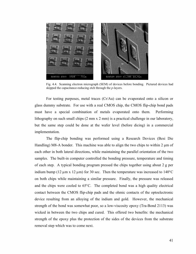
41
Fig. 4.4. Scanning electron micrograph (SEM) of devices before bonding. Pictured devices had skipped the capacitance-reducing etch through the p-layers.
For testing purposes, metal traces (Cr/Au) can be evaporated onto a silicon or
glass dummy substrate. For use with a real CMOS chip, the CMOS flip-chip bond pads
must have a special combination of metals evaporated onto them. Performing
lithography on such small chips (2 mm x 2 mm) is a practical challenge in our laboratory,
but the same step could be done at the wafer level (before dicing) in a commercial
implementation.
The flip-chip bonding was performed using a Research Devices (Besi Die
Handling) M8-A bonder. This machine was able to align the two chips to within 2 µm of
each other in both lateral directions, while maintaining the parallel orientation of the two
samples. The built-in computer controlled the bonding pressure, temperature and timing
of each step. A typical bonding program pressed the chips together using about 2 g per
indium bump (12 µm x 12 µm) for 30 sec. Then the temperature was increased to 140°C
on both chips while maintaining a similar pressure. Finally, the pressure was released
and the chips were cooled to 65°C. The completed bond was a high quality electrical
contact between the CMOS flip-chip pads and the ohmic contacts of the optoelectronic
device resulting from an alloying of the indium and gold. However, the mechanical
strength of the bond was somewhat poor, so a low-viscosity epoxy (Tra-Bond 2113) was
wicked in between the two chips and cured. This offered two benefits: the mechanical
strength of the epoxy plus the protection of the sides of the devices from the substrate
removal step which was to come next.
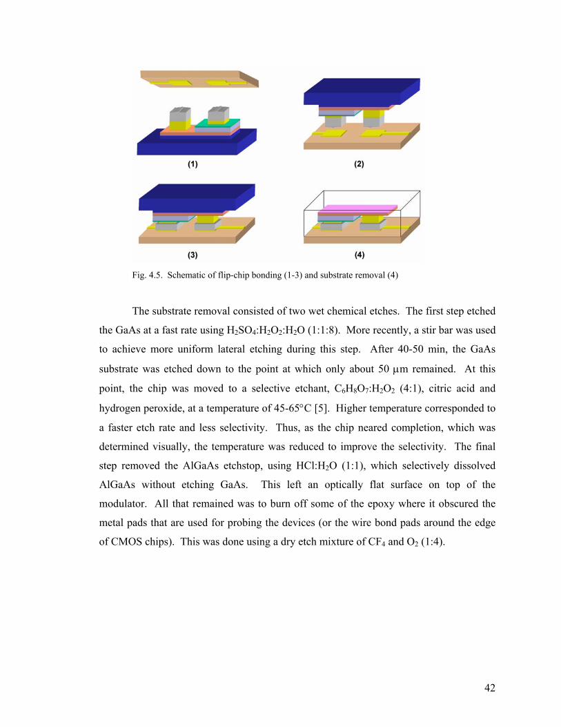
42
Fig. 4.5. Schematic of flip-chip bonding (1-3) and substrate removal (4)
The substrate removal consisted of two wet chemical etches. The first step etched
the GaAs at a fast rate using H2SO4:H2O2:H2O (1:1:8). More recently, a stir bar was used
to achieve more uniform lateral etching during this step. After 40-50 min, the GaAs
substrate was etched down to the point at which only about 50 µm remained. At this
point, the chip was moved to a selective etchant, C6H8O7:H2O2 (4:1), citric acid and
hydrogen peroxide, at a temperature of 45-65°C [5]. Higher temperature corresponded to
a faster etch rate and less selectivity. Thus, as the chip neared completion, which was
determined visually, the temperature was reduced to improve the selectivity. The final
step removed the AlGaAs etchstop, using HCl:H2O (1:1), which selectively dissolved
AlGaAs without etching GaAs. This left an optically flat surface on top of the
modulator. All that remained was to burn off some of the epoxy where it obscured the
metal pads that are used for probing the devices (or the wire bond pads around the edge
of CMOS chips). This was done using a dry etch mixture of CF4 and O2 (1:4).

43
Fig. 4.6. Scanning electron micrograph (SEM) of finished modulators flip-chip bonded to CMOS
At this point, the devices were ready for testing. A probe station enabled a
voltage to be placed across a row of devices. In fact, on the test structures, it was
possible to place the devices in forward bias at which point they behave like light
emitting diodes (LEDs). By forward biasing all the devices in an array simultaneously, it
was simple to observe the yield of the device array. Greater than 97 % yield was
observed in the best test chips, though better results (> 4300 working devices on a single
chip) have been published by the group at Bell Labs [3], indicating improvements are
certainly possible.
Fig. 4.7. Array of AlGaAs modulators in forward bias, showing > 97% yield

44
To investigate the properties of one device, interesting information was obtained
by varying both the voltage bias across the device and the wavelength of the incident CW
laser while recording the reflectivity of the modulator. For this purpose a tunable
Ti:Sapphire laser was employed and the measurement was entirely controlled by a
computer. Fig. 4.8 is a typical plot from such an experiment.
Fig. 4.8. Reflectivity of AlGaAs modulators vs. wavelength at different reverse biases
Two effects can clearly be seen in this plot. First there is the QCSE, which
appears as the change in absorption between 845 nm and 855 nm due to the changing
voltage. More dramatic, though, is the second effect – the dips in overall reflectivity
around 838 nm and 888 nm and the reflectivity peak at 860 nm. This is caused by the
Fabry-Perot cavity formed between the lower mirror of the Au p-contact and the top
mirror of the semiconductor-air interface (about a 30 % reflector). On the device shown
in Fig 4.8, this effect is clearly a nuisance, reducing both the change in reflectivity and
the contrast ratio. Many groups have avoided this problem by depositing an anti-
reflection (AR) coating to the top surface. However, it is possible to turn this nuisance
into an advantage by specifically designing the Fabry-Perot cavity resonance to occur in
the same wavelength range as the device is supposed to operate (~845-855 nm).
Unfortunately, a few practical hurdles had to be overcome to achieve this.
0
0.1
0.2
0.3
0.4
0.5
0.6
0.7
0.8
0.9
830 840 850 860 870 880 890Wavelength (nm)
Ref
lect
ivity
0 Volts1 Volt2 Volts3 Volts4 Volts5 Volts6 Volts

45
4.4 ASYMMETRIC FABRY-PEROT MODULATORS Several groups in the early and mid-1990’s developed asymmetric Fabry-Perot
modulators (AFPMs), generally in this AlGaAs/GaAs same material system [6-11].
Normally, the goal was to lower the voltage drive while improving the contrast ratio. As
such, peak contrast ratios greater than 20 dB (100:1) were observed [6, 7]. Most
modulators that have claimed “low voltage operation” in the literature refer to a voltage
drive 4 V or greater. These low voltage designs also have quite small wavelength ranges,
sometimes a fraction of a nanometer (e.g. [6]). Perhaps the best result in the literature is
the modulator of Yan et al. [9]. This device used only 2 V drive to achieve a contrast
ratio of 3 dB over 5 nm, with a peak contrast of 7 dB (5:1). Theoretical studies also
looked at optimizing these modulators [12-15].
While these results are quite impressive in many regards, our goals were slightly
different. For short distance optical interconnects, it makes more sense to achieve decent
contrast ratio over a wide range of wavelengths than to post an extremely high contrast
ratio for a small range of wavelengths, as discussed in Chapter 3. Furthermore, since the
epitaxial growth techniques are complicated and expensive, a simpler, thinner epitaxial
structure would be more practical and less costly in both time and dollars. Finally, the
thickness of a layer in an epitaxial structure cannot be perfectly determined during the
growth. Variations in conditions, especially temperature, cause variations in thickness
and composition that can easily alter the absorption characteristics of the MQW region by
several nanometers in wavelength. Thus we were faced with the challenge of developing
both a mathematical handle on a simple AFPM and a practical post-growth experimental
technique for adjusting to growth variations.
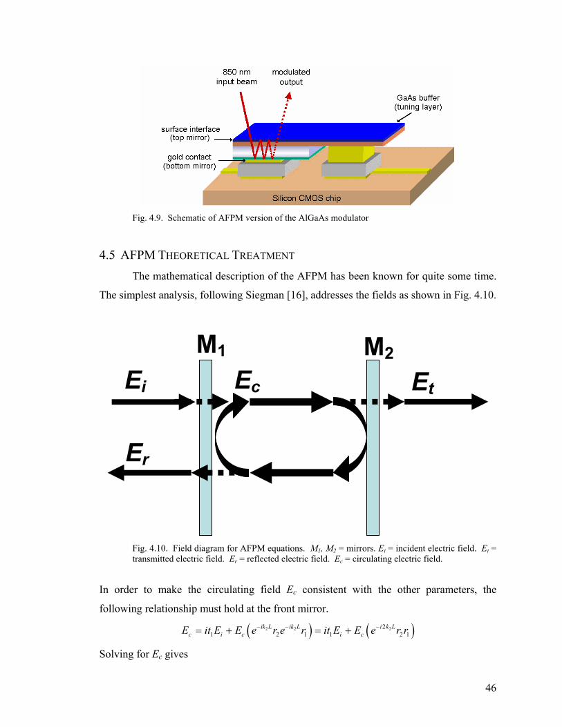
46
Fig. 4.9. Schematic of AFPM version of the AlGaAs modulator
4.5 AFPM THEORETICAL TREATMENT The mathematical description of the AFPM has been known for quite some time.
The simplest analysis, following Siegman [16], addresses the fields as shown in Fig. 4.10.
Fig. 4.10. Field diagram for AFPM equations. M1, M2 = mirrors. Ei = incident electric field. Et = transmitted electric field. Er = reflected electric field. Ec = circulating electric field.
In order to make the circulating field Ec consistent with the other parameters, the
following relationship must hold at the front mirror.
( ) ( )2 2 221 2 1 1 2 1
ik L ik L i k Lc i c i cE it E E e r e r it E E e r r− − −= + = +
Solving for Ec gives
Ei
Er
Ec Et
M1 M2
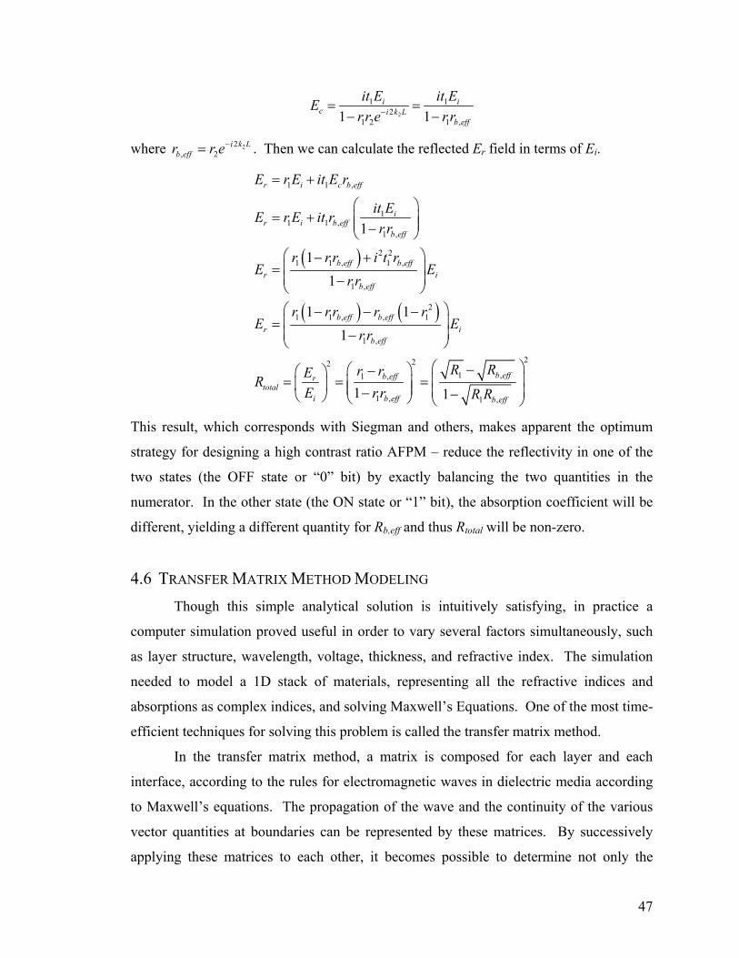
47
2
1 12
1 2 1 ,1 1i i
c i k Lb eff
it E it EEr r e r r−= =
− −
where 22, 2
i k Lb effr r e−= . Then we can calculate the reflected Er field in terms of Ei.
( )
( ) ( )
1 1 ,
11 1 ,
1 ,
2 21 1 , 1 ,
1 ,
21 1 , , 1
1 ,
221 ,
1 ,
1
11
1 11
1
r i c b eff
ir i b eff
b eff
b eff b effr i
b eff
b eff b effr i
b eff
b effrtotal
i b eff
E r E it E r
it EE r E it rr r
r r r i t rE E
r r
r r r r rE E
r r
r rERE r r
= +
= + − − + = − − − − = −
− = = −
2
1 ,
1 ,1b eff
b eff
R R
R R
− = −
This result, which corresponds with Siegman and others, makes apparent the optimum
strategy for designing a high contrast ratio AFPM – reduce the reflectivity in one of the
two states (the OFF state or “0” bit) by exactly balancing the two quantities in the
numerator. In the other state (the ON state or “1” bit), the absorption coefficient will be
different, yielding a different quantity for Rb,eff and thus Rtotal will be non-zero.
4.6 TRANSFER MATRIX METHOD MODELING Though this simple analytical solution is intuitively satisfying, in practice a
computer simulation proved useful in order to vary several factors simultaneously, such
as layer structure, wavelength, voltage, thickness, and refractive index. The simulation
needed to model a 1D stack of materials, representing all the refractive indices and
absorptions as complex indices, and solving Maxwell’s Equations. One of the most time-
efficient techniques for solving this problem is called the transfer matrix method.
In the transfer matrix method, a matrix is composed for each layer and each
interface, according to the rules for electromagnetic waves in dielectric media according
to Maxwell’s equations. The propagation of the wave and the continuity of the various
vector quantities at boundaries can be represented by these matrices. By successively
applying these matrices to each other, it becomes possible to determine not only the

48
reflection and transmission characteristics of the dielectric stack, but also the electric
fields or intensities as a function of distance inside the stack [17].
The software package MATLAB is optimized for matrix manipulation, so many
calculations can be done in sequence, enabling optimization routines that run in real time.
For example, the thickness of a particular layer can be altered between 100 and 200 nm in
steps of only 1 nm, and the entire simulation can still finish in seconds. Effects such as
the Gaussian beam profile of the laser focus can also be included by superposing plane
waves.
For the refractive indices, published values were typically used where available,
especially equations for interpolating the index for AlxGa1-xAs. The MQW region was
approximated as a bulk material with a complex index of refraction corresponding to its
absorption, derived from the following experimental procedure. First a p-i-n diode test
structure was processed. Then the device was inserted into our probe station setup and
the photocurrent was measured as the voltage across the diode and the wavelength of an
incident laser were varied. Assuming that every photon subtracted from the optical beam
corresponded exactly to one electron-hole pair collected electrically, the effective
absorption coefficient of the MQW region can be calculated [1]. Then adjustments to the
refractive index of the MQW region are derived via the Kramers-Kronig relations. These
steps result in data of the effective absorption coefficient and refractive index of the
MQW region as a function of wavelength. In the transfer matrix simulations, the MQW
region was thus approximated as a quasi-bulk material with a complex refractive index
that varied as a function of both wavelength and reverse bias.
4.7 EXPERIMENTAL TECHNIQUE OF CAVITY TUNING In order to simplify the growth during molecular beam epitaxy (MBE), we
designed the minimum number of layers. The design required a p-i-n diode with MQWs
in the intrinsic region plus an etchstop layer for the substrate removal. The use of the p-
contact as a reflective surface avoided a DBR growth. (The metal stack included Au as
the material directly in contact with the GaAs p-cap in order to maximize the reflectivity
at that interface.) The top mirror is formed just from the semiconductor-air interface.
Another possibility would have been to deposit a dielectric mirror on the top of the GaAs

49
buffer, after the substrate removal, to increase the top mirror reflectivity, as in [18].
However, the deposition of a dielectric mirror was undesirable for our design because by
keeping the top mirror reflectivity low, the device maintains a wide wavelength range.
If a dielectric mirror was to be avoided, it remained necessary to adjust to growth
variations, once the epitaxial growth has been completed. A post-integration cavity
thickness tuning technique was developed to solve this problem [19]. Essentially, the
strategy was deliberately to grow the structure a little too thick, to fabricate the device
structures, to measure the positions of the Fabry-Perot and exciton peaks, and finally to
remove a small amount of semiconductor material in a highly controlled fashion in order
to shift the Fabry-Perot resonance to the appropriate wavelength.
Using the transfer matrix method simulation approach described earlier, the
device could be designed to take advantage of the resonant effect. The device processing
steps had, by this point, become well-understood. The position of the Fabry-Perot and
exciton peaks could be observed using the tunable Ti:sapphire laser in the probe station in
the optics lab before the epoxy removal step (i.e. with no applied bias). Clearly the
critical step was the final one – removing a small amount of semiconductor in a
controlled manner. The key was to use a highly selective wet etch that removed only the
native oxide layer that formed on the surface of GaAs without etching GaAs [20]. An
added benefit of this etching technique is that it has been shown to smooth the surface by
a factor of about 5-10 (from rms roughness of 10-20 Å down to ~2 Å). Because the
oxide layer is formed only through the first few monolayers of the surface and can be
selectively removed, the cavity thickness can be carefully tuned by increments equal to
this oxide thickness (~10-20 Å).
The procedure for cavity tuning was then clear. Once the devices were fabricated,
flip-chip bonded, and exposed via substrate removal, the etchstop was removed by a 90 s
dip in HCl:H2O (1:1). This exposed the GaAs buffer layer, which was intentionally
grown a bit too thick, as noted previously. An oxide was formed by a 30 s dip in H2O2
and selectively removed by a 30 s etch in HCl:H2O (1:1) or NH4OH:H2O (1:9) [20]. We
refer to this as one “tuning cycle.” Fig. 4.11 below shows the result of both 2 tuning
cycles (blue curve) and of 10 tuning cycles (green curve) with respect to the original
absorption vs. wavelength data (red curve). The movement of the Fabry-Perot resonance
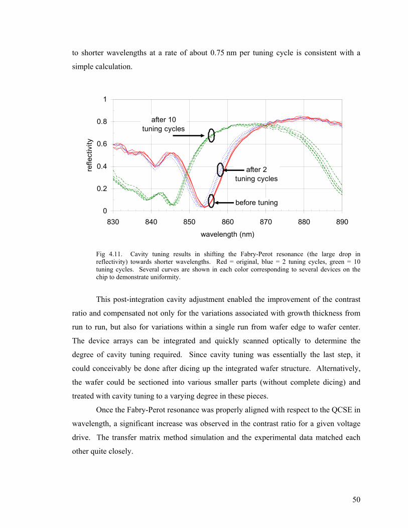
50
to shorter wavelengths at a rate of about 0.75 nm per tuning cycle is consistent with a
simple calculation.
Fig 4.11. Cavity tuning results in shifting the Fabry-Perot resonance (the large drop in reflectivity) towards shorter wavelengths. Red = original, blue = 2 tuning cycles, green = 10 tuning cycles. Several curves are shown in each color corresponding to several devices on the chip to demonstrate uniformity.
This post-integration cavity adjustment enabled the improvement of the contrast
ratio and compensated not only for the variations associated with growth thickness from
run to run, but also for variations within a single run from wafer edge to wafer center.
The device arrays can be integrated and quickly scanned optically to determine the
degree of cavity tuning required. Since cavity tuning was essentially the last step, it
could conceivably be done after dicing up the integrated wafer structure. Alternatively,
the wafer could be sectioned into various smaller parts (without complete dicing) and
treated with cavity tuning to a varying degree in these pieces.
Once the Fabry-Perot resonance was properly aligned with respect to the QCSE in
wavelength, a significant increase was observed in the contrast ratio for a given voltage
drive. The transfer matrix method simulation and the experimental data matched each
other quite closely.
0
0.2
0.4
0.6
0.8
1
830 840 850 860 870 880 890
wavelength (nm)
refle
ctiv
ity
before tuning
after 2 tuning cycles
after 10 tuning cycles
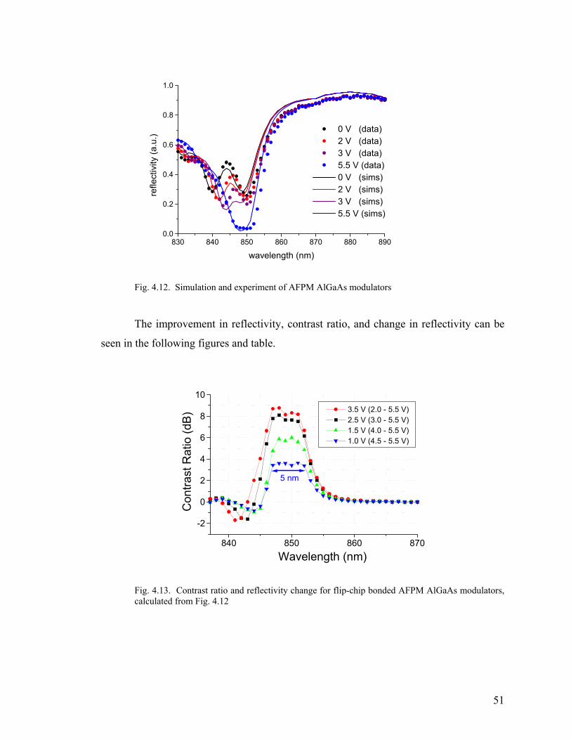
51
Fig. 4.12. Simulation and experiment of AFPM AlGaAs modulators
The improvement in reflectivity, contrast ratio, and change in reflectivity can be
seen in the following figures and table.
840 850 860 870
-2
0
2
4
6
8
10
5 nm
3.5 V (2.0 - 5.5 V) 2.5 V (3.0 - 5.5 V) 1.5 V (4.0 - 5.5 V) 1.0 V (4.5 - 5.5 V)
Con
trast
Rat
io (d
B)
Wavelength (nm)
Fig. 4.13. Contrast ratio and reflectivity change for flip-chip bonded AFPM AlGaAs modulators, calculated from Fig. 4.12
830 840 850 860 870 880 8900.0
0.2
0.4
0.6
0.8
1.0
0 V (data) 2 V (data) 3 V (data) 5.5 V (data) 0 V (sims) 2 V (sims) 3 V (sims) 5.5 V (sims)
refle
ctiv
ity (a
.u.)
wavelength (nm)
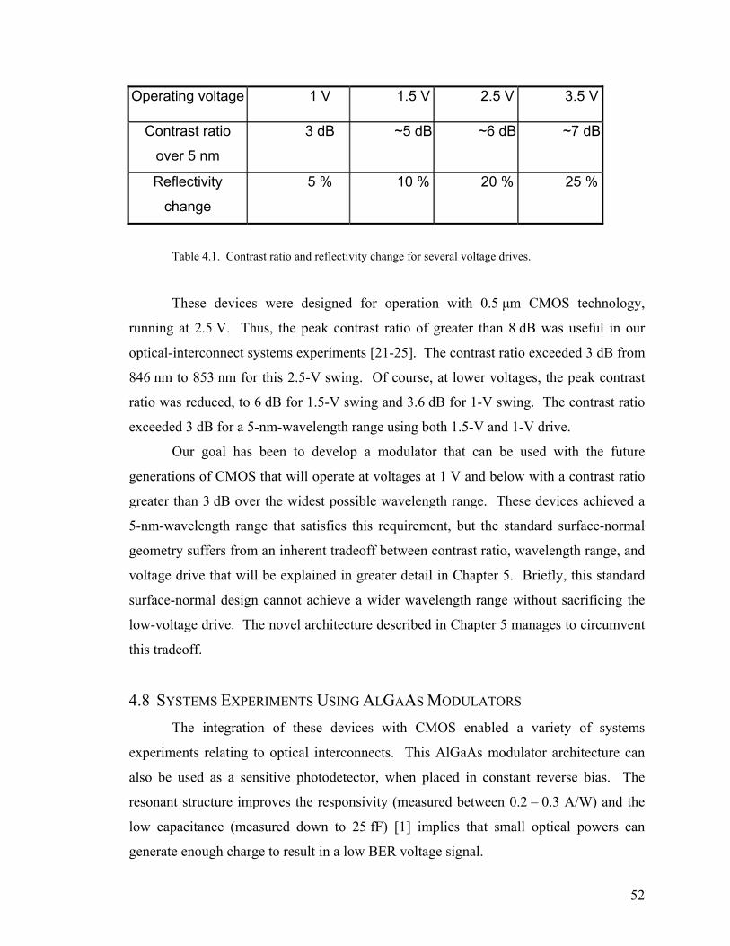
52
Operating voltage 1 V 1.5 V 2.5 V 3.5 V
Contrast ratio
over 5 nm
3 dB ~5 dB ~6 dB ~7 dB
Reflectivity
change
5 % 10 % 20 % 25 %
Table 4.1. Contrast ratio and reflectivity change for several voltage drives.
These devices were designed for operation with 0.5 µm CMOS technology,
running at 2.5 V. Thus, the peak contrast ratio of greater than 8 dB was useful in our
optical-interconnect systems experiments [21-25]. The contrast ratio exceeded 3 dB from
846 nm to 853 nm for this 2.5-V swing. Of course, at lower voltages, the peak contrast
ratio was reduced, to 6 dB for 1.5-V swing and 3.6 dB for 1-V swing. The contrast ratio
exceeded 3 dB for a 5-nm-wavelength range using both 1.5-V and 1-V drive.
Our goal has been to develop a modulator that can be used with the future
generations of CMOS that will operate at voltages at 1 V and below with a contrast ratio
greater than 3 dB over the widest possible wavelength range. These devices achieved a
5-nm-wavelength range that satisfies this requirement, but the standard surface-normal
geometry suffers from an inherent tradeoff between contrast ratio, wavelength range, and
voltage drive that will be explained in greater detail in Chapter 5. Briefly, this standard
surface-normal design cannot achieve a wider wavelength range without sacrificing the
low-voltage drive. The novel architecture described in Chapter 5 manages to circumvent
this tradeoff.
4.8 SYSTEMS EXPERIMENTS USING ALGAAS MODULATORS The integration of these devices with CMOS enabled a variety of systems
experiments relating to optical interconnects. This AlGaAs modulator architecture can
also be used as a sensitive photodetector, when placed in constant reverse bias. The
resonant structure improves the responsivity (measured between 0.2 – 0.3 A/W) and the
low capacitance (measured down to 25 fF) [1] implies that small optical powers can
generate enough charge to result in a low BER voltage signal.

53
The ultrashort pulses from a modelocked Ti:sapphire laser reduced the latency of
a chip-to-chip optical interconnect [22], improved the receiver sensitivity [24], and
enabled a WDM interconnect using spectral slicing [25]. These optoelectronic devices
can also be utilized in clock-distribution networks as low-capacitance photodetectors
[23], or as high-speed diagnostic tools, in a “pump-probe” configuration [26].
4.9 SUMMARY Low-voltage surface-normal modulators are attractive devices for optical
interconnects. Using a simple simulation technique, the transfer matrix method,
asymmetric Fabry-Perot AlGaAs/GaAs modulators improved the contrast ratio over a 5 -
10-nm-wavelength range significantly, while maintaining a low-voltage drive between 1 -
2.5 V. These modulators were enabled by a uniquely developed processing technique
we term cavity tuning, a reliable post-integration method for aligning the optical
resonance with the MQW exciton peak. In the future, CMOS technology will push
operating voltages down to 1 V and below, before optical interconnects become a reality,
illuminating the need for modulators that maintain contrast ratio while operating on such
a low-voltage drive.

54
REFERENCES [1] G. A. Keeler, "Optical Interconnects to Silicon CMOS: Integrated Optoelectronic
Modulators and Short Pulse Systems," Ph.D. Dissertation in Department of Applied Physics, Stanford University, Stanford, CA, 2002.
[2] A. L. Lentine, K. W. Goossen, J. A. Walker, L. M. F. Chirovsky, L. A. DAsaro, S. P. Hui, B. T. Tseng, R. E. Leibenguth, D. P. Kossives, D. W. Dahringer, D. D. Bacon, T. K. Woodward, and D. A. B. Miller, "Arrays of optoelectronic switching nodes comprised of flip-chip-bonded MQW modulators and detectors on silicon CMOS circuitry.," IEEE Photonics Technology Letters, vol. 8, pp. 221-3, 1996.
[3] A. L. Lentine, K. W. Goossen, J. A. Walker, L. M. F. Chirovsky, L. A. DAsaro, S. P. Hui, B. J. Tseng, R. E. Leibenguth, J. E. Cunningham, W. Y. Jan, J. M. Kuo, D. W. Dahringer, D. P. Kossives, D. Bacon, G. Livescu, R. L. Morrison, R. A. Novotny, and D. B. Buchholz, "High-speed optoelectronic VLSI switching chip with >4000 optical I/O based on flip-chip bonding of MQW modulators and detectors to silicon CMOS.," IEEE Journal on Selected Topics in Quantum Electronics, vol. 2, pp. 77-84, 1996.
[4] K. W. Goossen, J. A. Walker, L. A. Dasaro, S. P. Hui, B. Tseng, R. Leibenguth, D. Kossives, D. D. Bacon, D. Dahringer, L. M. F. Chirovsky, A. L. Lentine, and D. A. B. Miller, "GaAs MQW modulators integrated with silicon CMOS.," IEEE Photonics Technology Letters, vol. 7, pp. 360-2, 1995.
[5] M. Tong, D. G. Ballegeer, A. Ketterson, E. J. Roan, K. Y. Cheng, and I. Adesida, "A comparative study of wet and dry selective etching processes for GaAs/AlGaAs/InGaAs pseudomorphic MODFETs.," Journal of Electronic Materials, 1991 Electronic Materials Conference; Boulder, CO, USA, vol. 21, pp. 9-15, 1992.
[6] D. S. Gerber, R. Droopad, and G. N. Maracas, "A GaAs/AlGaAs asymmetric Fabry-Perot reflection modulator with very high contrast ratio.," IEEE Photonics Technology Letters, vol. 5, pp. 55-8, 1993.
[7] K. K. Law, R. H. Yan, L. A. Coldren, and J. L. Merz, "Self-electro-optic device based on a superlattice asymmetric Fabry-Perot modulator with an on/off ratio >100:1.," Applied Physics Letters, vol. 57, pp. 1345-7, 1990.
[8] K. K. Law, M. Whitehead, J. L. Merz, and L. A. Coldren, "Simultaneous achievement of low insertion loss, high contrast and low operating voltage in asymmetric Fabry-Perot reflection modulator.," Electronics Letters, vol. 27, pp. 1863-5, 1991.
[9] R. H. Yan, R. J. Simes, and L. A. Coldren, "Extremely low-voltage Fabry-Perot reflection modulators.," IEEE Photonics Technology Letters, vol. 2, pp. 118-19, 1990.
[10] J. A. Trezza, B. Pezeshki, M. C. Larson, S. M. Lord, and J. S. Harris, Jr., "High contrast asymmetric Fabry-Perot electro-absorption modulator with zero phase change.," Applied Physics Letters, vol. 63, pp. 452-4, 1993.
[11] M. G. Xu, T. A. Fisher, J. M. Dell, and A. Clark, "Wide optical bandwidth asymmetric Fabry-Perot reflection modulator using the quantum confined Stark effect.," Journal of Applied Physics, vol. 84, pp. 5761-5, 1998.

55
[12] B. Pezeshki, D. Thomas, and J. S. Harris, "Novel cavity design for high reflectivity changes in a normally off electroabsorption modulator.," Applied Physics Letters, vol. 58, pp. 813-15, 1991.
[13] A. K. Tipping, G. Parry, and A. J. Moseley, "Modelling the optimum performance of InGaAs/InP-based asymmetric Fabry-Perot modulator devices.," Semiconductor Science and Technology, vol. 5, pp. 525-9, 1990.
[14] P. Zouganeli, P. J. Stevens, D. Atkinson, and G. Parry, "Design trade-offs and evaluation of the performance: attainable by GaAs-Al{sub 0.3}Ga{sub 0.7}As asymmetric Fabry-Perot modulators.," IEEE Journal of Quantum Electronics, vol. 31, pp. 927-43, 1995.
[15] P. Zouganeli, M. Whitehead, P. J. Stevens, A. W. Rivers, G. Parry, and J. S. Roberts, "High tolerances for a low-voltage, high-contrast, low-insertion-loss asymmetric Fabry-Perot modulator.," IEEE Photonics Technology Letters, vol. 3, pp. 733-5, 1991.
[16] A. E. Siegman, Lasers. Sausalito, CA: University Science Books, 1986. [17] M. Gerken, "Wavelength multiplexing by spatial beam shifting in multilayer thin-
film structures," Ph.D. Dissertation in Department of Electrical Engineering, Stanford University, Stanford, CA, 2003.
[18] Z. Karim, C. Kyriakakis, A. R. Tanguay, R. F. Cartland, K. Hu, L. Chen, and A. Madhukar, "Postgrowth tuning of inverted cavity InGaAs/AlGaAs spatial light modulators using phase compensating dielectric mirrors," Applied Physics Letters, vol. 66, pp. 2774-2776, 1995.
[19] G. A. Keeler, N. C. Helman, P. Atanackovic, and D. A. B. Miller, "Cavity resonance tuning of asymmetric Fabry-Perot MQW modulators following flip-chip bonding to silicon CMOS," presented at Optics in Computing, Taipei, Taiwan, 2002.
[20] C. Zhang, D. Lubyshev, T. N. Jackson, D. L. Miller, and T. S. Mayer, "The effect of Al{sub 0.7}Ga{sub 0.3}As etch stop removal on the preparation of wafer-bonded compliant substrates.," Journal of the Electrochemical Society, vol. 146, pp. 1597-601, 1999.
[21] H. Chin, G. A. Keeler, N. C. Helman, M. Wistey, D. A. B. Miller, and J. S. Harris, Jr., "Differential optical remoting of ultrafast charge packets using self-linearized modulation.," presented at LEOS 2002. 2002 IEEE/LEOS Annual Meeting Conference Proceedings. 15th Annual Meeting of the IEEE Lasers and Electro-Optics Society, 10-14 Nov. 2002, Glasgow, UK, 2002.
[22] D. Agarwal, G. A. Keeler, C. Debaes, B. E. Nelson, N. C. Helman, and D. A. B. Miller, "Latency reduction in optical interconnects using short optical pulses.," IEEE Journal of Selected Topics in Quantum Electronics, vol. 9, pp. 410-18, 2003.
[23] C. Debaes, A. Bhatnagar, D. Agarwal, R. Chen, G. A. Keeler, N. C. Helman, H. Thienpont, and D. A. B. Miller, "Receiver-less optical clock injection for clock distribution networks.," IEEE Journal of Selected Topics in Quantum Electronics, vol. 9, pp. 400-9, 2003.
[24] G. A. Keeler, B. E. Nelson, D. Agarwal, C. Debaes, N. C. Helman, A. Bhatnagar, and D. A. B. Miller, "The benefits of ultrashort optical pulses in optically
56
interconnected systems.," IEEE Journal of Selected Topics in Quantum Electronics, vol. 9, pp. 477-85, 2003.
[25] B. E. Nelson, G. A. Keeler, D. Agarwal, N. C. Helman, and D. A. B. Miller, "Wavelength division multiplexed optical interconnect using short pulses.," IEEE Journal of Selected Topics in Quantum Electronics, vol. 9, pp. 486-91, 2003.
[26] G. A. Keeler, D. Agarwal, C. Debaes, B. E. Nelson, N. C. Helman, H. Thienpont, and D. A. B. Miller, "Optical pump-probe measurements of the latency of silicon CMOS optical interconnects.," IEEE Photonics Technology Letters, vol. 14, pp. 1214-16, 2002.
57
CHAPTER 5 : QUASI-WAVEGUIDE ANGLED-FACET
ELECTROABSORPTION MODULATOR
5.1 INTRODUCTION Future CMOS technology is clearly moving towards digital voltage levels of 1 V.
The ITRS Roadmap indicates an expected off-chip speed of 9.5 GHz and a voltage of
1.0 V in 2010 [1]. By 2016, the ITRS predicts the voltage will only have dropped to
0.8 V while the off-chip speed will have increased to around 36 GHz [1]. In addition,
current long-haul and medium-haul optical networks utilize WDM fiber-based systems
operating at a wavelength around 1550 nm and at bit rates of 10 Gbps. If the future of
both personal computing and telecommunications involves optical networks, it seems
natural to expect these two types of networks to seamlessly integrate.
In order to design a surface-normal modulator for optical interconnects, several
factors must be taken into consideration, as described in Chapter 3. The AlGaAs
modulator from Chapter 4 achieved a good contrast ratio of ~ 6 dB for a 5-nm-
wavelength range around 850 nm, but required 2.5 V of voltage drive. Lowering the
voltage drive to 1 V reduced the contrast ratio to ~3 dB for 5 nm. This standard surface-
normal design is subject to a tradeoff between contrast ratio, wavelength range, and low
voltage operation, discussed below. In order to achieve a contrast ratio of 3 dB over a
wider wavelength range without dramatically increasing the voltage drive, some new
strategy must be employed.
These considerations, very low voltage drive and compatibility with larger C-
band WDM optical networks, led us to design a high-speed, low-voltage modulator
operating at 1550 nm. This novel modulator architecture, called a quasi-waveguide
angled-facet electroabsorption modulator (QWAFEM), and its advantages will be
presented in this chapter, followed by a description of the methods of its design,
fabrication, and testing.
5.1.1 LOW VOLTAGE OPERATION
A surface-normal modulator that operates on only 1 V of digital voltage swing
must be extremely thin in order to achieve a high electric field change across the MQW

58
region. However, a thin MQW region results in a low contrast ratio, unless an optical
resonator is implemented surrounding it, as in the AFPM discussed in Chapter 4. As the
quality factor of the AFPM resonator is increased, the contrast ratio improves, but the
wavelength range is limited. A high contrast ratio for a low voltage swing is possible at
the expense of the wavelength range, as in [2] where a contrast ratio of 10 dB for 1 V was
achieved across less than 1 nm of wavelength range. Note that, for a given quality factor,
the wavelength range increases for shorter cavities, as shown in Fig. 5.1.
Fig. 5.1. AFPM simulation for two cavity thicknesses: reflectivity vs. wavelength. Both modulators have identical MQW regions and mirrors, but the thickness of the resonator is larger on the right. These plots demonstrate that the wavelength range (represented here by the drop in reflectivity) is wider for shorter Fabry-Perot cavities.
It seems the ideal modulator would have a thin MQW region (in order to allow a
large change in the electric field for a small voltage swing) and a short Fabry-Perot
optical cavity with highly reflective mirrors (in order to achieve a high contrast ratio
while maintaining the maximum possible wavelength range). Unfortunately, in a
surface-normal geometry (i.e. the light propagation axis perpendicular to the epitaxial
layers), the penetration depth of dielectric mirrors can be many wavelengths on each side,
making a very short optical cavity impossible. Metallic mirrors can be utilized instead,
but they suffer from absorption.
This dilemma, the tradeoff between contrast ratio, low voltage, and wavelength
range, seems inherent to surface-normal modulators, but it is avoided in waveguide
modulators.

59
5.1.2 COMPATIBILITY WITH LARGER OPTICAL NETWORKS
Since long-haul optical networks operate at wavelengths in the telecom C-band
(1535 nm – 1565 nm) at high bit rates (≥ 10 Gbps), any modulator compatible with this
network must also operate at those wavelengths and speeds. Achieving high speed
simply consumes more power in driving the modulator capacitance – experiments with
modulators operating at speeds upwards of 50 GHz (e.g. [3]), even as high as 250 GHz
[4], indicate no basic physical barrier to surface-normal modulators running at such
speeds.
Modulating a 1550 nm laser beam using the electroabsorption effect requires a
semiconductor material system with a bandgap wavelength in that range. Most
telecommunications semiconductor devices use the InGaAsP/InP system, though some
work has also been done on InAlGaAs/InP [5]. The major drawback of designing
modulators for 1550 nm (compared to 850 nm) is the greatly reduced absorption
coefficient. The absorption coefficient of an InGaAsP/InP quantum well is generally
about 3 times lower than that of equivalent AlGaAs/GaAs quantum well. (Recent
developments in the GaInNAs(Sb)/GaAs system may eventually eliminate this problem
[6]. See Chapter 6 for a brief discussion of this material system and its characteristics for
electroabsorption modulators.)
1460 1480 1500 1520 1540 1560 15800
1000
2000
3000
4000
14 V/µm
8 V/µm
2 V/µm
0 V/µm
Abs
orpt
ion
coef
ficie
nt (c
m-1)
Wavelength (nm)
Fig. 5.2. Quantum-confined Stark effect for InGaAsP MQW grown on InP. Absorption coefficient vs. wavelength for three values of the applied electric field in the MQW.
60
The problem of a relatively low absorption coefficient is essentially what necessitates the
use of the AFPM concept in the first place. The fact that the absorption coefficient of
InGaAsP is 3 times lower than AlGaAs makes it significantly more difficult to achieve
the goal of a high contrast ratio over a wide wavelength range for a low voltage drive.
5.1.3 SUMMARY OF REQUIREMENTS
For compatibility with larger optical networks, it would be useful for a modulator
for optical interconnects to operate at wavelengths near 1550 nm. For compatibility with
future CMOS, a voltage drive below 1 V is required. In addition, this ideal modulator for
optical interconnects should achieve a contrast ratio of at least 3 dB (for good signal-to-
noise ratio) over a wavelength range of at least 10 nm (for use with WDM networks or
uncooled laser sources). The architecture should allow for 2D arrays of devices with
surface-normal optical and electrical access while reducing fabrication, integration, and
packaging costs of the entire system.
5.2 PREVIOUS WORK ON 1550 NM SURFACE-NORMAL MODULATORS All previous attempts to design surface-normal optoelectronic modulators
operating at 1550 nm have failed to achieve a high contrast ratio over a wide wavelength
range using a low voltage drive – three requirements for an optical interconnects
transmitter.
Some groups, such as Yoo et al. [7] and Onodera et al. [2], achieve a high contrast
ratio with a low voltage drive with AFPM structures. The first modulator reached 15 dB
of contrast with a low voltage drive of 2 volts, but the wavelength range was restricted to
approximately 1 nm [7]. The second design produced a contrast ratio of 10 dB using
only 1 V of drive, but operated over a wavelength range that was just a fraction of a
nanometer [2].
Thick MQW regions can help overcome the low absorption coefficient of the
InGaAsP/InP material system, but at the expense of requiring more voltage to shift the
absorption to longer wavelengths. One prime example of such a design was published by
Pathak et al. in 1994 [8]. That modulator displayed a peak contrast ratio of 9 dB but

61
required 50 V reverse bias to switch between states. The contrast ratio exceeded 3 dB
over a large wavelength range of 23 nm.
5.3 QWAFEM: AN INTRODUCTION 5.3.1 DESCRIPTION AND ADVANTAGES OF QWAFEM
Fig. 5.3. QWAFEM schematic (not to scale)
The quasi-waveguide angled-facet electroabsorption modulator (QWAFEM) [9]
is shown in the schematic in Fig. 5.3. As in the AlGaAs modulator architecture of
Chapter 4, the device is simply a p-i-n diode grown on a semiconductor substrate;
however, there are a couple of major differences. First, the device operates at a
wavelength at which the substrate is transparent. For example, a QWAFEM modulator
can be fabricated in the InGaAsP/InP material system for operation in the C-band. At
these wavelengths, the InP substrate is nominally transparent and thus the light can be
passed through it with a small amount of attenuation. (Note that this substrate-
transparency requirement can be satisfied for other materials and substrates, such as
InGaAs/GaAs at 980 nm wavelength.) Second, two angled mirrors are etched into the
substrate at an angle steeper than 45°, such that the laser beam reflects off one, passes
through the diode at a shallow angle, bounces off the epitaxial surface, back through the
diode and reflects off the other mirror before propagating back through the substrate.

62
The substrate has such a high refractive index (n ~ 3.17) that all three reflections are
lossless due to total internal reflection (TIR).
By combining the desirable features of a surface-normal modulator with those of
a standard waveguide design, the QWAFEM achieves many of the requirements laid out
above. The QWAFEM is a 1550 nm surface-normal modulator that is simple to fabricate
and integrate with CMOS. The tradeoff between contrast ratio, wavelength range, and
voltage drive is avoided, due to the large incident angle, as discussed below. Thus,
similar to the waveguide geometry, a high contrast ratio over a wide wavelength range
can be achieved even for a low voltage drive. This physically small modulator can be
made in dense 2D arrays for high data rate transmission. Two specific aspects of this
design are discussed in the following sections: the QWAFEM’s misalignment tolerance
and the effect of the large incident angle of the laser beam upon the p-i-n diode.
5.3.2 MISALIGNMENT TOLERANCE
The three-bounce geometry is inherently insensitive to translational
misalignments between the device and the incoming laser beam as shown in Fig. 5.4, as
long as the two mirrors are etched at precisely equivalent angles, relative to the z-
direction. (The two mirrors can be etched at equivalent angles using, for example, a wet
etching technique that will selectively reveal a particular crystal plane of the substrate.
See section 5.8.) Lateral movement of the device in the x-direction is ignored by the
optical system, since the input and output beams maintain a fixed distance with respect to
each other. (Angular misalignments are discussed briefly in section 5.9.5.) The finite
size of the device and its angled mirrors can be designed to accommodate the desired
misalignment tolerance. This feature would reduce the cost of packaging these
modulator arrays in an optical system, in comparison with the stringent alignment
requirements of waveguide devices.

63
Fig. 5.4. Misalignment tolerance geometry of QWAFEM. Two paths of the light beam are shown. First, in solid line and centered on the mirrors, and second, in dotted line and off-center, shifted to the left.
5.3.3. LARGE INCIDENT ANGLE
The shallow angle of propagation of the laser beam with respect to the p-i-n diode
epitaxial layer structure (i.e. the large angle of incidence with respect to the normal)
results in an increased interaction between the light and the absorbing MQW region in
three ways, in comparison with a standard surface-normal modulator. First, in the ray
optics picture, the light simply travels through more of the MQW region by virtue of the
angle of its propagation.
Fig. 5.5. Geometry of ray optics factor of 1/cos(θ).
θι
L
L/cos(θi)

64
Second, the large incident angle causes a larger amount of power to be reflected
from interfaces between layers with small differences in refractive index. One of the
challenges of using the InGaAsP system for optical devices is the small difference in
refractive index between InP (n ~ 3.17) and InGaAs (n ~ 3.55). In the pure surface-
normal case, this results in a low power reflectivity of just 0.3%:
2 2
21 2
1 2
3.55 3.17 (0.057) 0.0032 0.3%3.55 3.17
n nRn n
− − = = = = = + + .
However, at large incident angles, the power reflectivity rises significantly, even for a
single interface. For example, the same calculation can be done for an incident angle of
70°. The power reflectivity at this angle is ~ 8 %, a 25-fold increase. In terms of making
a modulator, the high reflectivity simplifies AFPM designs, as we shall see in the
QWAFEM. An added complication is that InGaAs is absorbing at the wavelengths of
interest. Thus we are constrained to using InGaAsP material with a bandgap of ~ 0.9 eV
(which corresponds to a wavelength of 1.38 µm and is commonly denoted “1.38 Q”) and
a refractive index of approximately n = 3.45.
Fig. 5.6. Power reflectivity vs. incident angle for a single interface of InP (n = 3.17) and InGaAsP (n = 3.45)
θi
n = 3.17
n = 3.45
65
Third, the standing-wave pattern generated by the beam’s self-interference at the
interface between the epitaxy and the air can be used to improve the overlap between the
optical intensity and the MQW absorbing material. A shallower propagation angle
(larger incident angle) implies that the intensity interference pattern will be longer in the
z-direction. This interference pattern can be correctly positioned to overlap with the
MQW region in the location of maximum optical intensity.
5.4 ANGLE PROPAGATION AFPM AND SIMULATIONS Both the mathematical derivation and the transfer matrix method simulation can
easily be modified to include the propagation of the optical wave at an angle relative to
the epitaxial layer structure. The wave is propagating in the x-z plane and, as such, has
components of its wavevector ˆ ˆx zk k x k z= + in both the x- and z-directions. These two
directions are separable and because the structure is homogeneous in the x- and y-
directions, only the z-direction needs to be solved. The solutions in the x- and y-
directions are simply plane waves, while the solution in the z-direction will be a
complicated function of the properties of the layer structure, such as complex refractive
indices, layer thicknesses, incident angle, etc.
The transfer matrix method simulations described in Chapter 4 were modified to
include the incident angle and are included as Appendix B. The Gaussian beam
approximation was used to simulate the incoming laser beam as a collection of plane
waves with the same wavelength but with a Gaussian distribution of wavevectors in a
particular phase relationship [10].
Using this simulation program, many different designs were tested. For the
MQW region, a p-i(MQW)-n diode structure was fabricated and tested. The resulting
photocurrent was converted into an absorption coefficient and refractive index, as
described in Chapter 4. In addition, n-doped layers were added to create an optical
resonator structure around the i-MQW region.

66
1460 1480 1500 1520 1540 15600
1000
2000
3000
4000
8.8 V/µm
4.4 V/µm
0 V/µm
Abs
orpt
ion
coef
ficie
nt (c
m-1)
Wavelength (nm)
Fig. 5.7. Absorption coefficient vs. wavelength for three values of the applied electric field: 0, 4.4 and 8.8 V/µm
The following figures demonstrate the effect of the resonator structure that was designed
for the QWAFEM. Fig. 5.8a is a modulator with the gold mirror on the bottom (as in the
Chapter 4 design). With a 1-V drive, this design modulates the reflectivity between 85-
95 % for a contrast ratio of 0.5 dB. If the beam is incident at an angle of 70° from normal
and the design is reoptimized for this condition (Fig. 5.8b), the 1/cos(θ) factor improves
the modulation to between 75-93 % for a contrast ratio of 0.9 dB. Including a 3-pair
DBR above the MQW region creates an AFPM structure that greatly increases the
interaction between the optical field and the MQW region. The resulting modulation of
reflectivity between 12-25 % achieves a contrast ratio of 3.2 dB.

67
a.)
b.)
c.)
Fig. 5.8. Simulated intensity in various structures: Red = high intensity, blue = low intensity. a.) Surface-normal modulator with gold mirror. b.) Angled-facet modulator without resonator, incident angle 70°, showing standing wave effect where beam interferes with itself. Note difference in scale between axes. c.) Angled-facet modulator with DBR, incident angle 70°, showing DBR layers and increased intensity inside MQW region. Note difference in scale between axes.
8 QW
Gold
InP substrat
MQW
MQW
DBR

68
Clearly, the addition of the 3-pair DBR mirror and resonator improves the
contrast ratio significantly. Why not, then, continue to increase the reflectivity of the
epitaxial mirror? In a standard surface-normal AFPM, increasing the reflectivity of the
mirrors, raises the quality factor and limits the wavelength range that is resonant inside
the device. As shown previously in Fig. 5.1, shorter Fabry-Perot cavities maintain a
wider wavelength range. The QWAFEM is, effectively, a second-order cavity – there are
only two intensity maxima in the z-direction inside the resonator. (The finite penetration
depth of the DBR (~250 nm) must be taken into account.) Increasing the quality factor in
the QWAFEM does not appreciably limit the wavelength range as much as it limits the
angular range of the plane waves that are resonant. Fig. 5.9 shows how increasing the
quality factor (by increasing the number of DBR pairs) improves the depth of the
resonance, while sacrificing its width.
Fig. 5.9. Angular resonance as a function of the number of DBR pairs: 1 pair (red), 2 pairs (black), and 3 pairs (blue)
The narrow angular resonance for large incident angles can be seen
mathematically as follows. First, it must be noted that the resonant effect, either surface-
normal or at an angle, is sensitive to the amount of phase accumulated in the z-direction.
In both cases, raising the AFPM mirror reflectivities will cause the design to be more
sensitive to the accumulated phase. This can be considered to be due to the increased

69
effective cavity length – the average photon spends more time in the cavity, and is thus
more sensitive to the accumulated phase. As a measure of this phase, we can consider the
wavevector component in the z-direction, kz, and ask what changes in wavelength and
incident angle result in certain fractional changes in kz. In other words, if we know that a
given cavity is sensitive to 1 % changes in kz, then we can study the magnitude of
changes in wavelength and incident angle that result is such a 1 % fractional change.
Since 2 cosz ink π θ
λ= , we can calculate the fractional change in kz in the following
manner.
tan
tan
z z
z
z
zz
zi
z
k k
kkk k
kk
λ λλλ
θθ
θ θ
∂= −
∂∂ ∂
= −
∂= −
∂∂
= −∂
For a surface-normal design, θi = 0, so a small change in angle ∂θ from this center
angle value does not cause a significant fractional change in kz. A fractional change in
wavelength causes an equal fractional change in kz. At large incident angles, however,
there is a significant effect. For example, at θi = 70°, tan θi = 2.75. Consider a 1 %
change in λ. This still causes a 1% change in kz, but it is equivalent to a fractional
angular deviation of ∂θ = 0.01/tan θi = 0.2 degrees.
This angular resonance poses an interesting tradeoff. The angular resonance (of
the 3-pair DBR) is 4-5 degrees wide, implying that the incoming beam needs to be
aligned to within about one degree of the design angle. In the QWAFEM, this is
straightforward because of the method of etching the angled mirrors, described later in
this chapter, as long as the incoming beam can be aligned to within about 3 degrees of the
normal incidence that is expected. This is due to Snell’s Law: the higher refractive index
of the semiconductor substrate with respect to the air or glass substrate of the optical
system improves the angular range of the input by the ratio of the indices of refraction.
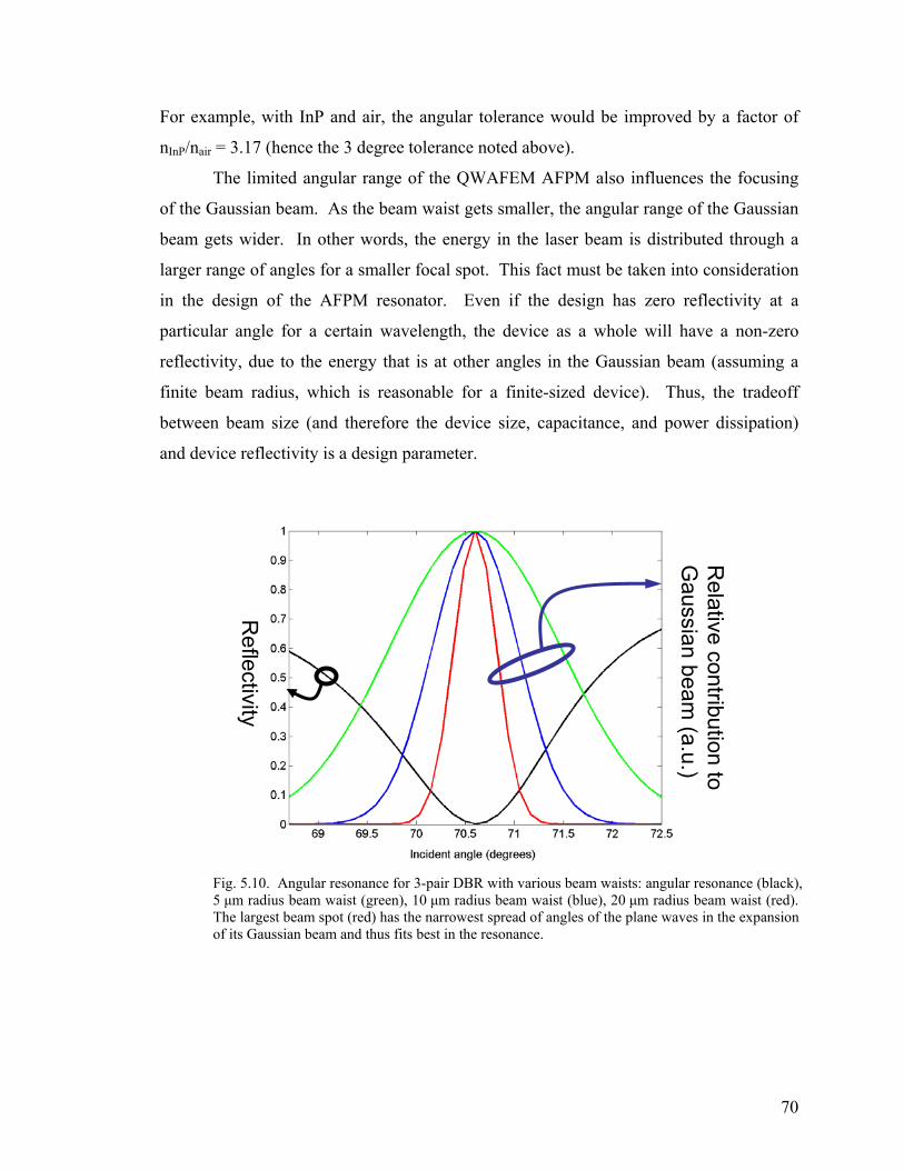
70
For example, with InP and air, the angular tolerance would be improved by a factor of
nInP/nair = 3.17 (hence the 3 degree tolerance noted above).
The limited angular range of the QWAFEM AFPM also influences the focusing
of the Gaussian beam. As the beam waist gets smaller, the angular range of the Gaussian
beam gets wider. In other words, the energy in the laser beam is distributed through a
larger range of angles for a smaller focal spot. This fact must be taken into consideration
in the design of the AFPM resonator. Even if the design has zero reflectivity at a
particular angle for a certain wavelength, the device as a whole will have a non-zero
reflectivity, due to the energy that is at other angles in the Gaussian beam (assuming a
finite beam radius, which is reasonable for a finite-sized device). Thus, the tradeoff
between beam size (and therefore the device size, capacitance, and power dissipation)
and device reflectivity is a design parameter.
Fig. 5.10. Angular resonance for 3-pair DBR with various beam waists: angular resonance (black), 5 µm radius beam waist (green), 10 µm radius beam waist (blue), 20 µm radius beam waist (red). The largest beam spot (red) has the narrowest spread of angles of the plane waves in the expansion of its Gaussian beam and thus fits best in the resonance.
Reflectivity
Relative contribution to
Gaussian beam
(a.u.)
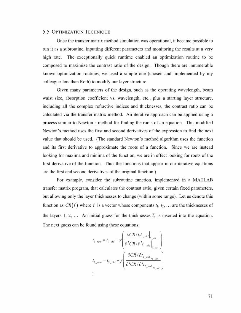
71
5.5 OPTIMIZATION TECHNIQUE Once the transfer matrix method simulation was operational, it became possible to
run it as a subroutine, inputting different parameters and monitoring the results at a very
high rate. The exceptionally quick runtime enabled an optimization routine to be
composed to maximize the contrast ratio of the design. Though there are innumerable
known optimization routines, we used a simple one (chosen and implemented by my
colleague Jonathan Roth) to modify our layer structure.
Given many parameters of the design, such as the operating wavelength, beam
waist size, absorption coefficient vs. wavelength, etc., plus a starting layer structure,
including all the complex refractive indices and thicknesses, the contrast ratio can be
calculated via the transfer matrix method. An iterative approach can be applied using a
process similar to Newton’s method for finding the roots of an equation. This modified
Newton’s method uses the first and second derivatives of the expression to find the next
value that should be used. (The standard Newton’s method algorithm uses the function
and its first derivative to approximate the roots of a function. Since we are instead
looking for maxima and minima of the function, we are in effect looking for roots of the
first derivative of the function. Thus the functions that appear in our iterative equations
are the first and second derivatives of the original function.)
For example, consider the subroutine function, implemented in a MATLAB
transfer matrix program, that calculates the contrast ratio, given certain fixed parameters,
but allowing only the layer thicknesses to change (within some range). Let us denote this
function as ( )CR t where t is a vector whose components t1, t2, … are the thicknesses of
the layers 1, 2, … An initial guess for the thicknesses 0t is inserted into the equation.
The next guess can be found using these equations:
1_
1_
2 _
2 _
1_
1_ 1_ 2 21_
2 _
2 _ 2_ 2 22_
/
/
/
/
old
old
old
old
old tnew old
old t
old tnew old
old t
CR tt t
CR t
CR tt t
CR t
γ
γ
∂ ∂ = + ∂ ∂ ∂ ∂ = + ∂ ∂
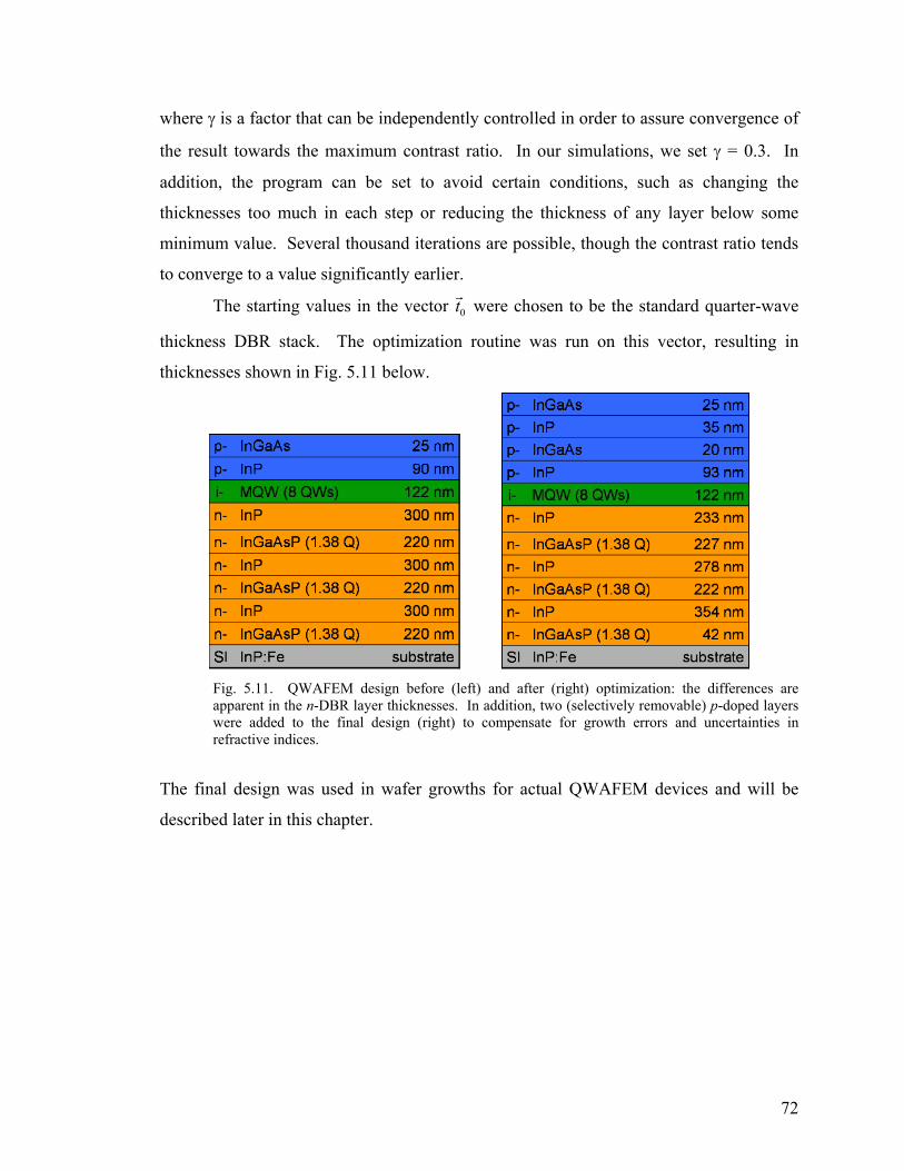
72
where γ is a factor that can be independently controlled in order to assure convergence of
the result towards the maximum contrast ratio. In our simulations, we set γ = 0.3. In
addition, the program can be set to avoid certain conditions, such as changing the
thicknesses too much in each step or reducing the thickness of any layer below some
minimum value. Several thousand iterations are possible, though the contrast ratio tends
to converge to a value significantly earlier.
The starting values in the vector 0t were chosen to be the standard quarter-wave
thickness DBR stack. The optimization routine was run on this vector, resulting in
thicknesses shown in Fig. 5.11 below.
Fig. 5.11. QWAFEM design before (left) and after (right) optimization: the differences are apparent in the n-DBR layer thicknesses. In addition, two (selectively removable) p-doped layers were added to the final design (right) to compensate for growth errors and uncertainties in refractive indices.
The final design was used in wafer growths for actual QWAFEM devices and will be
described later in this chapter.

73
1460 1480 1500 1520 1540 1560 15800
1
2
3
4
5
6
0.8 V drive:(4.4 V/µm to 8.8 V/µm)
23 nmC
ontra
st ra
tio (d
B)
Wavelength (nm)
Fig. 5.12. Simulation of optimized design using MQW data from previous runs and using a (then-believed correct) value of n = 3.50 for the InGaAsP (1.38 Q) material across all wavelengths
5.6 WAFER GROWTH VARIATIONS The last issue to discuss in regards to the design of QWAFEMs is the variation of
layer thickness and material composition during the wafer growth. Our semiconductor
epitaxial material is grown by metallorganic chemical vapor deposition (MOCVD). Even
the most skilled crystal growth engineers cannot control the thickness of a particular layer
to within 1 % of its target, due primarily to the extreme sensitivity of the growth rate to
temperature variations [11]. Thus, the final QWAFEM wafer design must be tolerant to
variations in layer thickness and material composition on the order of 2 %. Because our
simulation model can run so quickly, it is simple to extend the simulation to run in a
mode where it changes the thicknesses by ± 2 %. These simulated results showed
acceptable results even for these variations. Additional thin layers were added to the top
of the structure which can be selectively removed via wet etching should it be necessary
to compensate for such variations.
5.7 WAFER GROWTH AND TESTING The optimized wafer design in Fig. 5.11 was grown via MOCVD at Agilent Labs
by David Bour. The n-doped region contains the 3-pair DBR of alternating layers of InP
and In0.70Ga0.30As0.66P0.34 (1.38 Q). The n-dopant S was added in a concentration of
74
5 x 10¹⁸ per cm3. Judging from reported data [12], this InGaAsP layer was assumed to
have a constant index of refraction of n = 3.50 across the wavelength range of interest.
The quantum wells were 85-Å wide and composed of In0.60Ga0.40As0.85P0.15. The
barriers between the wells were 60-Å wide and composed of In0.82Ga0.18As0.39P0.61. The
entire MQW region (8 wells and 9 barriers) was 122-nm thick and was nominally
intrinsic (i.e. unintentionally doped). The p-doped region consisted of a 93-nm InP layer,
followed by shorter alternating layers of InGaAs and InP, which were included in order
to have the option of tuning the thickness of the cavity via selective wet etching.
Variations in expected growth thickness, material composition and refractive index,
exciton wavelength/band edge, and substrate mirror etch angle could be somewhat
compensated by this coarse cavity tuning. The p-dopant Zn was added in a concentration
of 5 x 10¹⁷ per cm3 and offset 45 nm from the i-MQW region to avoid significant Zn
diffusion into the intrinsic region.
5.8 FABRICATION
The fabrication of QWAFEM arrays was a six-mask process performed in the
Ginzton Microfabrication Facility, Stanford Nanofabrication Facility (SNF), and with
help from Ning Cao at the Electrical Engineering Department at University of California
at Santa Barbara (UCSB). A summary of the process is presented here, and the extended
set of details is included as Appendix C.
5.8.1 MESA ETCH AND N-CONTACTS
First, metal alignment marks were precisely aligned to the crystal planes of the
InP substrate and were deposited on the wafer via a liftoff process. Next, mesa structures
were etched down through the i-MQW region into the first n-InP layer using selective
wet etchants (H2SO4:H2O2:H2O (1:2:10) for etching InGaAsP and MQW, HCl for InP).
This isolated the various modulator diodes from each other electrically. The mesas were
60-µm wide and 120-µm long, although this size was chosen somewhat arbitrarily for the
device testing. The physical size of the device determines its capacitance and thus its
power dissipation. Clearly, for use in an actual system, the devices should be reduced
significantly in size. After the mesa etch, n-contacts were evaporated and lifted off.
75
5.8.2 ETCHING ANGLED MIRRORS
The key steps in fabricating QWAFEM arrays created the angled mirrors. It was
critical that these angled facets be as smooth as possible and at the designed (54.7°) angle
with respect to the top wafer surface. The chemistry between the etchant, the substrate,
and the mask material must not allow undercutting of the substrate at the mask-substrate
interface. We developed two similar methods for etching these mirrors. A technique
using a Ti mask, similar to that of [13], will be described first.
5.8.2.1 Ti mask angled mirror procedure
First, the area where the angled mirrors were to be etched must be cleared of any
epitaxial layers. 500 nm of SiO2 was deposited via plasma-enhanced chemical vapor
deposition (PECVD). Rows on opposite sides of the mesas were exposed via lithography
and the SiO2 layer was etched in the SNF’s drytek4 plasma etcher using a mixture of
CHF3 and O2. At this point, the wafer was packaged and sent to UCSB to etch the
remaining epitaxial layers, the n-DBR. Ning Cao at UCSB etched through these layers
using their Unaxis plasma etcher.
When the wafers returned to Stanford, the SiO2 mask was removed in buffered
oxide etch (essentially HF:H2O (1:6) buffered to maintain a constant pH during etching)
for 5 min. At this point, lithography outlined the p-contacts, which were evaporated and
lifted off. The fabrication of the angled mirrors continued by allowing the native oxide to
form by exposure to air for ~24 hours. A 40-nm layer of Ti was evaporated as an etch
mask before lithography defined the position of the angled mirrors. The Ti layer was
etched in dilute HF:H2O (1:100), exposing the InP substrate below, into which the angled
mirrors are subsequently formed by a 20-24 min etch in HBr.

76
Fig. 5.13. Microscope image (top view) of three devices before V-grooves were etched. Each device is 60 µm wide and 120 µm long.
Due to the zinc-blende crystal structure of InP, some acids, such as HBr, etch
certain crystal planes faster than others. Generally, the (111)A crystal plane is etched
most slowly, because it contains the highest percentage of In atoms, which are less
reactive than the P atoms that are exposed more in other crystal planes [14]. The crystal
plane (111)A lies at a 54.7° angle with respect to the (100) plane of the top of the wafer.
Thus, the etching revealed a V-shaped groove in the InP substrate [13-17]. The
alignment of the entire structure with respect to this (111)A plane was critical [16] and
must be done at the first step of processing (metal alignment marks). However, the
angled facets that were exposed were often not smooth enough to be mirror-quality.
Fig. 5.14. (left) Edge view of V-grooved sample, microscope image. (right) Top view of V-grooved sample showing 3 rows of 5 devices each with V-grooves between rows.
InP
air V-groove
5 QWAFEMs

77
Fig. 5.15. SEM of rough angled facets
A second etch procedure was used to achieve smoother surfaces [13]. A mixture
of HBr:K2Cr2O7 (1:1) at 65°C was used along with HBr. By etching the wafer alternately
in these two liquids for varying times, a significantly smoother surface was achieved.
The rms roughness before the smoothing step (measured on a Zygo white light
interferometer) was typically 200 nm. Clearly, this surface remained too rough for use as
a mirror. Following the smoothing procedure, however, the rms roughness was improved
and dropped to 5-10 nm, even when measured over 60-100 µm distances, in the best case
scenario.
30 µm

78
Fig. 5.16. SEM of smooth angled facets on a sample that has been cleaved so that the V-shaped edge profile can be seen in the bottom third of the image while the smooth sidewalls are shown above
When complete, the angled facets were significantly larger (~60-100 µm) than the optical
beam incident upon them (~20-30 µm 1/e2 beam diameter).
A few factors contributed to the proper formation of the V-grooves and smooth
angled mirrors. Most importantly, the undercutting of the mask must be prevented. Any
undercutting at the mask-substrate interface exposed non-(111) planes that were etched
by HBr at an elevated rate. Undercutting resulted in a failure either to expose the mirror
at the correct angle, or to generate a smooth surface at all. This deleterious effect was
suppressed, it seems, by ensuring a clean surface of InP on which the Ti was deposited.
Many experiments with new InP wafers yielded extremely smooth V-grooves, while
those etched in wafers that have undergone many previous processing steps often failed.
After the angled mirrors are smooth, the Ti mask was removed and the devices
were annealed at 410°C for 30 s to improve the quality of the ohmic contacts. The final
step was to deposit an AR coating on the wafer backside, where the laser light entered the
substrate. Though we do not have the perfect materials at Stanford for this process, a
makeshift AR coating of SiNx was applied via plasma-enhanced chemical vapor
deposition (PECVD), resulting in only 2-4 % reflection (a reduction from the standard
27 % reflection).
6 µm
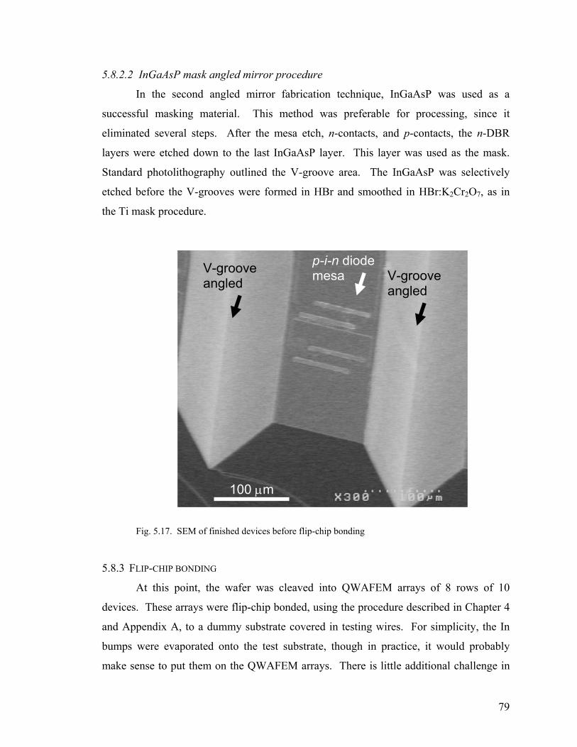
79
5.8.2.2 InGaAsP mask angled mirror procedure
In the second angled mirror fabrication technique, InGaAsP was used as a
successful masking material. This method was preferable for processing, since it
eliminated several steps. After the mesa etch, n-contacts, and p-contacts, the n-DBR
layers were etched down to the last InGaAsP layer. This layer was used as the mask.
Standard photolithography outlined the V-groove area. The InGaAsP was selectively
etched before the V-grooves were formed in HBr and smoothed in HBr:K2Cr2O7, as in
the Ti mask procedure.
Fig. 5.17. SEM of finished devices before flip-chip bonding
5.8.3 FLIP-CHIP BONDING
At this point, the wafer was cleaved into QWAFEM arrays of 8 rows of 10
devices. These arrays were flip-chip bonded, using the procedure described in Chapter 4
and Appendix A, to a dummy substrate covered in testing wires. For simplicity, the In
bumps were evaporated onto the test substrate, though in practice, it would probably
make sense to put them on the QWAFEM arrays. There is little additional challenge in
p-i-n diode mesa V-groove
angled
100 µm
V-groove angled
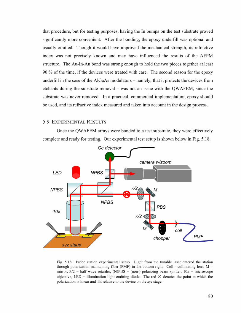
80
that procedure, but for testing purposes, having the In bumps on the test substrate proved
significantly more convenient. After the bonding, the epoxy underfill was optional and
usually omitted. Though it would have improved the mechanical strength, its refractive
index was not precisely known and may have influenced the results of the AFPM
structure. The Au-In-Au bond was strong enough to hold the two pieces together at least
90 % of the time, if the devices were treated with care. The second reason for the epoxy
underfill in the case of the AlGaAs modulators – namely, that it protects the devices from
etchants during the substrate removal – was not an issue with the QWAFEM, since the
substrate was never removed. In a practical, commercial implementation, epoxy should
be used, and its refractive index measured and taken into account in the design process.
5.9 EXPERIMENTAL RESULTS Once the QWAFEM arrays were bonded to a test substrate, they were effectively
complete and ready for testing. Our experimental test setup is shown below in Fig. 5.18.
Fig. 5.18. Probe station experimental setup. Light from the tunable laser entered the station through polarization-maintaining fiber (PMF) in the bottom right. Coll = collimating lens, M = mirror, λ/2 = half wave retarder, (N)PBS = (non-) polarizing beam splitter, 10x = microscope objective, LED = illumination light emitting diode. The red ⊗ denotes the point at which the polarization is linear and TE relative to the device on the xyz stage.
xyz stage
M
M
PBSNPBS
NPBS
NPBSLED
10x λ/2
λ/2
camera w/zoom
Ge detector
PMFcoll
chopper

81
The bonded QWAFEM array sat on a platform and was probed electrically using two
needle-like electrodes. These electrodes applied the reverse bias voltage across the
QWAFEMs and measured the photocurrent that was generated when the laser was on.
An Agilent tunable 1550-nm laser was routed onto the chip through polarization-
maintaining fiber and free-space optics (beamsplitters, mirrors, half-wave retarders, and a
microscope objective lens). The reflected beam was collected through the same objective
lens and imaged onto both a germanium detector and a phosphor IR camera. When the
optical beam was chopped, lock-in detection was used to filter out noise from the signal.
5.9.1 REFLECTIVITY AND CONTRAST RATIO
Varying the wavelength and voltage, we measured the reflectivity and contrast
ratio curves shown in Figs. 5.19 – 5.20.
1460 1480 1500 1520 1540 1560 1580
0.05
0.10
0.15
0.20
0.25
0.30
0.35
0.40 -0.3 V expt +0.5 V expt -0.3 V sim +0.5 V sim
Ref
lect
ivity
Wavelength (nm)
Fig. 5.19. Reflectivity of QWAFEM for 0.8-V drive between -0.3 V and 0.5 V reverse bias

82
1480 1500 1520 1540 15600
1
2
3
4
16 nm
0.8 V drive:-0.3 V to 0.5 V
Con
trast
ratio
(dB
)
Wavelength (nm)
Fig. 5.20. Contrast ratio of QWAFEM for 0.8-V drive
The peak of the contrast ratio with only 0.8 V of voltage drive was measured to be 3.7 dB.
More importantly, the contrast ratio was greater than 3 dB for 16 nm between 1498 nm
and 1514 nm. Unfortunately, the contrast ratio was not quite as high as designed because
it was not possible to measure the refractive index vs. wavelength of the quaternary
InGaAsP layer until after the modulator was already grown. Using reports in the
literature [12], we estimated its refractive index to be a constant 3.50, as stated above. It
was later measured at Agilent Labs by an advanced ellipsometry technique to be between
3.43 and 3.48 and to vary as a function of the wavelength. This variation is significant
enough to have caused a deviation from the expected reflectivity. Given this knowledge,
it would be possible to take this into consideration and repeat the experiment with a
modified design and achieve a higher contrast ratio.
Regardless, we have achieved our goal of 3 dB of contrast ratio across a 16-nm-
wavelength range using only a CMOS-compatible voltage drive of 0.8 V. Such a device
would be successful at transmitting signals at a low bit-error rate in an optical-
interconnect application. To the best of our knowledge, no other surface-normal
modulator offers such performance in the 1550-nm-wavelength range.

83
Author Year l (nm) Voltage
drive
Dl (nm)
(CR > 3 dB)
Peak
CR
Yoo 1998 1550 1.3 V 2 nm 10 dB
Onodera 2004 1550 1 V << 1 nm 10 dB
Pathak 1994 1550 50 V 23 nm 9 dB
Helman, Roth
2005 1550 0.8 V 16 nm 3.7 dB
Table 5.1 Comparison between previously-reported 1550-nm surface-normal modulators and QWAFEM. Our design, highlighted in green, satisfies all the requirements set out in Chapter 3, while previous designs fail in at least one category.
5.9.2 MISALIGNMENT TOLERANCE
As discussed in Chapter 3, waveguide modulators are expensive to package
because of the stringent demands on the alignment of the input and output fibers with
respect to the waveguide itself. Due to the three-bounce geometry of the QWAFEM, it is
inherently tolerant to misalignments in the x-y plane. The misalignment tolerance was
measured by translating the device in the x-y plane using a three-axis micrometer stage.
The reflectivity of the QWAFEM vs. displacement in the x-direction is shown in Fig.
5.22.
Fig. 5.21. Misalignment tolerance: QWAFEM reflectivity vs. lateral displacement. The FWHM of 30 µm is more than sufficient for practical applications. Asymmetry in the plot is likely caused by imperfections in the angled mirrors.
-60 -40 -20 0 20 40 60
0.0
0.2
0.4
0.6
0.8
1.0
30 µm
Nor
mal
ized
Ref
lect
ivity
(a.u
.)
Displacement along x-axis (µm)

84
The full-width at half-maximum (FWHM) of this curve is approximately 30 µm. In
contrast, the entire physical width of a waveguide modulator is approximately 3 µm and it
is common to require sub-µm alignment tolerance in the factory for these parts [18].
Judging from Dr. Goossen’s data [19], a misalignment tolerance of 10 µm should be
sufficient if the optical system mates to the CMOS chip using something akin to the
common MT connector.
5.9.3 CAPACITANCE, SPEED, AND POWER DISSIPATION
The capacitance of these test QWAFEM devices was measured by a C-V plotter
to be approximately 4 pF. This corresponds well with a simple calculation based on the
parallel-plate capacitor model. The capacitance can then be estimated as
2 2 120
(120µm)(60µm)(3.45) (8.85 10 F/m) 4.2pF(0.18µm)
A AC nd d
ε ε −= = = × = .
The value of the refractive index is an approximate bulk average real index for the
multiple-quantum-well intrinsic region and the thickness of the capacitor was taken to be
180 nm from the intended intrinsic region thickness, as grown.
For a 10-Gbps link, this capacitance implies a power consumption figure of
2 2 101 1
2 2(4 pF)(0.8 V) (10 bits/s) 12.8 mWP CV f= = = .
However, these devices were not optimized for size. Shrinking them by a factor of 2 in
each lateral dimension will reduce the power consumption to 3.2 mW per device. Of
course, there is a tradeoff in making the devices smaller, but it primarily comes out of the
misalignment tolerance budget. Since it seems that the misalignment tolerance can be
reduced and still maintain compatibility with a low-cost packaging solution, the power
budget for the modulator can also be reduced. If there is a total power budget for the chip
of 100 mW per link, the 3.2 mW consumed by the modulator itself plus less than 1 mW
of laser power per link seems quite reasonable.

85
5.9.4 INSERTION LOSS
The major sources of insertion loss in this device are likely to be scattering of the
laser from the angled mirrors and absorption in the n-InGaAsP (1.38 Q) DBR layers.
Insertion loss of about -7.2 dB was measured at 1512 nm in the device shown in
Fig. 5.19. From our simulations and supplemental experiments, we estimate that -3.5 dB
of loss was due to scattering from the angled facets, -2.9 dB of loss was caused by
absorption in the n-InGaAsP layers, and the remaining -0.3 dB was caused by residual
absorption in the MQW region. There was a negligible amount of loss from absorption in
the InP substrate.
The InP substrate absorption was determined by measuring the transmission of a
laser through a double-side polished InP wafer, AR-coated on both sides. Approximately
99 % of the light was transmitted through the wafer, indicating a maximum substrate
absorption of 1 %.
The issue of optical diffraction losses is somewhat less important as long as the
angled-facet mirror is significantly larger than the focused size of the Gaussian beam
when it hits the mirror. Though the beam might be clipped somewhat by the aperture
effect of the finite mirror, this is a design parameter that mostly affects the misalignment
tolerance. The relatively flat top of the misalignment tolerance shown in Fig. 5.21
indicates that most of the beam is probably being reflected by the angled mirror. If
practical devices would be made smaller, as discussed previously, then the issue of
diffraction would also become somewhat less significant since the light would have a
shorter distance to travel between the two angled mirrors.
5.9.5 ANGULAR ACCEPTANCE
The angular acceptance of the AFPM in this QWAFEM design is calculated to be
relatively narrow, at just 3 - 4 degrees, as shown in Fig. 5.9. A simple experiment
managed to measure this angular acceptance. A large mesa structure was fabricated in
the clean room and the edge of the wafer was polished at a 19.6° angle.

86
Fig. 5.22. Diagram of mesa structure and polishing
The probe station was modified to include a goniometer instead of the typical
sample stage, which allows the sample to be rotated about a fixed point 15.9 mm above
the center of the mount. The polished edge of the wafer was placed at this point and the
laser was directed to enter the mesa structure at the appropriate angle, normal to this
polished surface. Photocurrent measurements taken at various angles do indicate the
angular resonance of the structure with a FWHM of approximately a few degrees, as
expected theoretically.
goniometer
InP
n-contact p-contact p-i-n diode
mesa with n-DBR

87
-3.5 -3.0 -2.5 -2.0 -1.5 -1.0 -0.5 0.0 0.5 1.010
15
20
25
30
35
40
45
FWHM ~ 3-4 degreesPh
otoc
urre
nt (a
.u.)
Angle inside InP (degrees)
Fig. 5.23. Angular acceptance: (top) measurement of photocurrent in configuration shown in Fig. 5.22 showing a FWHM of 3 – 4 degrees. (bottom) simulation of the same effect, showing dip in reflectivity spectrum with FWHM of 4 – 5 degrees.
5.10 DRAWBACKS OF QWAFEM The two main cited “drawbacks” of QWAFEM are the polarization sensitivity and
the power consumption. The current QWAFEM architecture only modulates the TE
polarization. In practice, TE mode operation would not be a problem because the
modulator’s optical input would likely be a semiconductor diode laser. Semiconductor
diode lasers almost always run in the TE mode and the laser output would be routed
directly onto the QWAFEM array. One very likely scenario would be a high power
~ 4-5 degrees
88
semiconductor diode laser passing through a diffractive optical element to create a 2D
array of beams that could be imaged onto the QWAFEM array. In this case and in many
like it, the polarization of the laser would be well-known and determined before entering
the QWAFEM. The polarization sensitivity of the QWAFEM is only a problem if the
input laser beam is coming from, say, a non-polarization-maintaining fiber.
The QWAFEM is polarization sensitive due to both the quantum well design and
the resonator. The quantum wells were designed using InGaAsP layers lattice-matched
to InP, resulting in wells that preferentially absorb in the TE polarization at the longer
wavelengths. (The TM polarization still shows a nice excitonic effect at shorter
wavelengths due to the electron-light hole interaction.) The resonator is polarization
sensitive because of the phase on reflection at the total-internal-reflection interface
between the p-InGaAs and the air. This phase is different for the TE and TM
polarizations and thus the resonator was designed specifically for TE. It may be possible,
however, to figure out a resonator that accepts both polarizations and strained quantum
well designs are often used in waveguide modulators and switches to achieve
polarization-independent behavior.
The power consumption of the QWAFEM is certainly higher than that of the
AlGaAs modulators from Chapter 4, due to the QWAFEM’s higher capacitance. But it is
not quite a fair comparison. The QWAFEM has a misalignment tolerance of 30 µm. For
the AlGaAs modulators to achieve this tolerance, they would have to be significantly
larger, increasing capacitance. Secondly, they require more voltage to operate at a given
contrast ratio and the power consumption scales as V2. Though the power consumption is
a critical issue when many links are being made in parallel, the fact that a QWAFEM
array would be consuming less than 5 % of the link power budget seems reasonable.
Further reduction in the power consumption of the modulator itself would not
significantly lower the amount of heat that would need to be extracted from the entire
chip. Furthermore, improvements in the device design are certainly possible and several
of these will be presented in Chapter 6.

89
5.11 SUMMARY The QWAFEM architecture has proven to satisfy all of the needs of a modulator
for the application of optical interconnects. The QWAFEM achieved a contrast ratio of
3 dB over a 16-nm-wavelength range around λ = 1506 nm while requiring only 0.8-V
drive. This combination is, to the best of our knowledge, both unprecedented and
compatible with future optical interconnects requirements. The QWAFEM offers a
misalignment tolerance that can be determined by lithographic parameters and that has
been demonstrated up to 30 µm. The capacitance of 4 pF can easily be reduced to 1 pF
and would probably be pushed even lower in a commercial implementation. Finally, the
electrical power consumption is quite small compared to the power budget of each link.
90
REFERENCES
[1] Semiconductor Industry Association, "International Technology Roadmap for Semiconductors," http://public.itrs.net/Files/2003ITRS/Home.htm, 2003.
[2] A. Onodera, Y. Onishi, N. Nishiyama, C. Caneau, F. Koyama, and C. E. Zah, "Low-voltage operation of vertical-cavity intensity modulator using InP-based surface-emitting laser structure.," Japanese Journal of Applied Physics, Part 2 (Letters), vol. 43, pp. L806-7, 2004.
[3] R. Lewen, S. Irmscher, U. Westergren, L. Thylen, and U. Eriksson, "Segmented transmission-line electroabsorption modulators.," Journal of Lightwave Technology, vol. 22, pp. 172-9, 2004.
[4] S. Kodama, T. Yoshimatsu, and H. Ito, "500 Gbit/s optical gate monolithically integrating photodiode and electroabsorption modulator.," Electronics Letters, vol. 40, pp. 555-6, 2004.
[5] T. H. Stievater, W. S. Rabinovich, P. G. Goetz, R. Mahon, and S. C. Binari, "A surface-normal coupled-quantum-well modulator at 1.55 mu m.," IEEE Photonics Technology Letters, vol. 16, pp. 2036-8, 2004.
[6] V. Lordi, H. B. Yuen, S. R. Bank, and J. S. Harris, "Quantum-confined Stark effect of GaInNAs(Sb) quantum wells at 1300-1600 nm.," Applied Physics Letters, vol. 85, pp. 902-4, 2004.
[7] S. J. B. Yoo, M. A. Koza, R. Bhat, and C. Caneau, "1.5 mu m asymmetric Fabry-Perot modulators with two distinct modulation and chirp characteristics.," Applied Physics Letters, vol. 72, pp. 3246-8, 1998.
[8] R. N. Pathak, K. W. Goossen, J. E. Cunningham, and W. Y. Jan, "InGaAs-InP P-I (MQW)-N surface-normal electroabsorption modulators exhibiting better than 8:1 contrast ratio for 1.55- mu m applications grown by gas-source MBE.," IEEE Photonics Technology Letters, vol. 6, pp. 1439-41, 1994.
[9] N. C. Helman, Roth, J.E., Bour, D.P., Altug, H., Miller, D.A.B., "Misalignment-tolerant surface-normal low-voltage modulator for optical interconnects," IEEE Journal of Selected Topics in Quantum Electronics, vol. 11, pp. 338-342, 2005.
[10] M. Gerken, "Wavelength multiplexing by spatial beam shifting in multilayer thin-film structures," in Electrical Engineering. Stanford, CA: Stanford University, 2003.
[11] D. P. Bour, personal communication, 2004. [12] B. Jenson, Torabi, A., "Refractive index of quaternary InGaAsP lattice matched to
InP," Journal of Applied Physics, vol. 54, pp. 3623-3625, 1983. [13] P. Bonsch, D. Wullner, T. Schrimpf, A. Schlachetzki, and R. Lacmann,
"Ultrasmooth V-Grooves in InP by two-step wet chemical etching.," Journal of the Electrochemical Society, vol. 145, pp. 1273-6, 1998.
[14] S. Adachi, "Chemical etching of InP and InGaAsP/InP.," Journal of the Electrochemical Society, vol. 129, pp. 609-13, 1982.
[15] R. Klockenbrink, E. Peiner, H. H. Wehmann, and A. Schlachetzki, "Wet chemical etching of alignment V-grooves in (100) InP through titanium or In{sub 0.53}Ga{sub 0.47}As masks.," Journal of the Electrochemical Society, vol. 141, pp. 1594-9, 1994.
91
[16] J. Wang, D. K. Thompson, and J. G. Simmons, "Wet chemical etching for V-grooves into InP substrates.," Journal of the Electrochemical Society, vol. 145, pp. 2931-7, 1998.
[17] J. L. Weyher, R. Fornari, T. Gorog, J. J. Kelly, and B. Erne, "HBr-K{sub 2}Cr{sub 2}O{sub 7}-H{sub 2}O etching system for indium phosphide.," Journal of Crystal Growth, vol. 141, pp. 57-67, 1994.
[18] B. W. Hueners and M. K. Formica, "Photonic component manufacturers move toward automation.," Photonics Spectra, vol. 37, pp. 66-72, 2003.
[19] K. W. Goossen, "Fitting optical interconnects into an electrical world -- Packaging and reliability issues of arrayed optoelectronic modules," presented at LEOS 2004, Rio Grande, Puerto Rico, 2004.

92
CHAPTER 6 : IMPROVEMENTS AND FUTURE DIRECTIONS
The QWAFEM architecture achieved the goals set out in Chapter 3 for an ideal
modulator for short-distance optical interconnect links. The contrast ratio of 3 dB over a
16-nm-wavelength range using only a 0.8-V-logic-level drive is unprecedented
performance for a surface-normal semiconductor modulator. 2D arrays of QWAFEMs
were fabricated using standard techniques and flip-chip bonded successfully. The
surface-normal three-bounce geometry enables an inherent misalignment tolerance,
measured up to 30 µm.
Research on the QWAFEM design can now proceed in several directions. A
variety of ideas will be presented in this chapter.
6.1 QUANTUM WELL DESIGN The quantum wells used in our QWAFEM implementation were chosen because they
were known to have good QCSE characteristics. Parameters, such as well width, barrier
width, InGaAsP compositions and strain, could be varied in an attempt to improve the
device performance.
Advanced quantum well designs are also a possibility. Wider wells that include a
narrow barrier spike in the middle can be shown theoretically to lead to better QCSE [1-
6]. Quantum wells with an intra-well step also demonstrate theoretically improved
performance [7].
Fig. 6.1. New quantum well types: symmetric spiked, coupled well (left) and stepped well (right). Some designs utilize a hybrid version with asymmetric wells and a spike in the middle.
Continued research in quantum well designs is likely to lead to improved overall
device performance.

93
6.2 FRUSTRATED TIR QWAFEM 6.2.1 CONCEPT AND SIMULATIONS
One method of improving the performance of the QWAFEM design is to replace
the n-DBR layers with a very thin region with a low refractive index. The light, incident
at such a large angle (e.g. θi ~ 70°), would normally experience total internal reflection
(TIR) at this interface. However, if the low index material is thin enough, then some of
the light can tunnel into the active region and the TIR interface acts like a high
reflectivity mirror with some small (but important) amount of transmission.
Fig. 6.2. Schematic of frustrated TIR QWAFEM wafer structure
Such a device can easily be simulated and optimized by our MATLAB programs.
In order to make a fair comparison, we can simulate the QWAFEM structure using first
the standard design and second using frustrated TIR. In each case, we use the same
thickness and absorption coefficient data for the MQW region.
InP:Fe SI InGaAsP n- InP n- InGaAsP n- InP n- InGaAsP n- InP n- MQW i- InP p- p-InP 118 nm
i-MQW 122 nm
n-InP 118 nm
SiO2 107 nm
n-InP
substrate

94
1460 1480 1500 1520 1540 1560 15800
3
6
9
40 nm
0.8 V drive
Con
trast
ratio
(dB)
Wavelength (nm)
Fig. 6.3. Simulated contrast ratio vs. wavelength for frustrated TIR QWAFEM design
Clearly the frustrated TIR design is superior, achieving 3 dB of contrast ratio over
40 nm, greater than the width of the telecommunications C-band. The reasons for this
improvement are discussed below in Section 6.2.3.
6.2.2 FABRICATION METHODS FOR FRUSTRATED TIR QWAFEM
There are several possible methods for fabricating a frustrated TIR QWAFEM
structure. First, in order to use a single wafer and single epitaxial growth, the wafer
could be designed to include a sacrificial layer that could be removed via wet etching, as
is common in the fabrication of microelectromechanical systems (MEMS). A second
choice would involve wafer bonding. The thin air region could be etched off the top of
one wafer in the areas where the modulators are to be fabricated. Alternatively, thin
layers of another material, such as SiO2 could be deposited on one or both wafers, before
the bonding. As long as the interface between the substrate and this material results in a
TIR effect, any such material could be used. Such a technique has been developed by my
colleagues Michael Wiemer and Rafael Aldaz here at Stanford for an extended cavity
VCSEL using spin-on glass [8]. A third option consists of using flip-chip bonding to
combine the two wafers. In order to precisely control the thickness (around 90 – 130 nm)
of the low-index region, the flip-chip bonding technique would require calibration of the

95
thickness, a parameter that is typically ignored when the bonding is supposed to simply
electrically contact the two chips. The use of gold-gold bonding might be more relevant
in this case, or perhaps, just a very thin indium layer. More than likely, this can be
determined in practice, though we have not yet attempted to do it. Note that in all the
cases described above, it would be necessary to remove the p-i-n diode InP substrate after
bonding, but this can simply be done with a selective wet etch, such as HBr.
Using certain fabrication techniques, the ability to fabricate the angled mirrors
first, on a blank InP wafer, and confirm the angle and the roughness, before integrating
the p-i-n diode may enable better devices. Unfortunately, this would also lead to quicker
consumption of InP wafers and the need to remove one of the substrates. V-grooves in Si
[9] have also been widely used for optical fiber alignment. A hybrid technique that
combines two substrates such as this might be able to use (less expensive) Si substrates
for the V-grooves bonded to the p-i-n diode on an InP substrate.
6.2.3 ADVANTAGES
The advantages of a frustrated TIR QWAFEM would be continuous control of the
top mirror reflectivity (in the design phase), a true first-order Fabry-Perot cavity, and the
absence of absorption in the n-InGaAsP layers. The top mirror reflectivity can be
controlled as well as the fabrication method allows control of the thickness of the
tunneling layer (SiO2 or air). The lower penetration depth of the tunneling layer enables
the design of a true first-order cavity, whereas the penetration depth of the DBR structure
(~250 nm) necessitated a second-order cavity. This widens the wavelength range. In
addition, the insertion loss would be reduced due to the lack of the slightly-absorbing n-
InGaAsP DBR layers.
6.3 GAINNAS(SB) QWAFEM Recent electroabsorption data from Dr. Vincenzo Lordi in Prof. J.S. Harris’s
Group at Stanford is presented in Fig. 6.4.
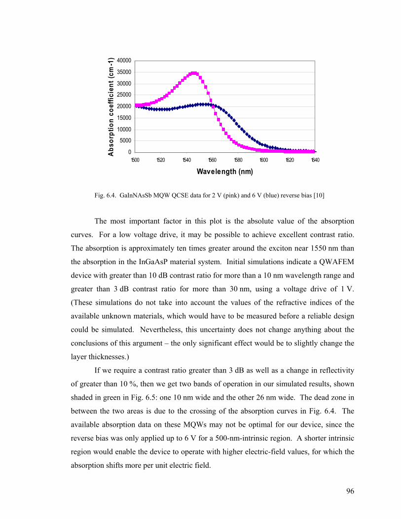
96
0
5000
10000
15000
20000
25000
30000
35000
40000
1500 1520 1540 1560 1580 1600 1620 1640
Wavelength (nm)
Abso
rptio
n co
effic
ient
(cm
-1)
Fig. 6.4. GaInNAsSb MQW QCSE data for 2 V (pink) and 6 V (blue) reverse bias [10]
The most important factor in this plot is the absolute value of the absorption
curves. For a low voltage drive, it may be possible to achieve excellent contrast ratio.
The absorption is approximately ten times greater around the exciton near 1550 nm than
the absorption in the InGaAsP material system. Initial simulations indicate a QWAFEM
device with greater than 10 dB contrast ratio for more than a 10 nm wavelength range and
greater than 3 dB contrast ratio for more than 30 nm, using a voltage drive of 1 V.
(These simulations do not take into account the values of the refractive indices of the
available unknown materials, which would have to be measured before a reliable design
could be simulated. Nevertheless, this uncertainty does not change anything about the
conclusions of this argument – the only significant effect would be to slightly change the
layer thicknesses.)
If we require a contrast ratio greater than 3 dB as well as a change in reflectivity
of greater than 10 %, then we get two bands of operation in our simulated results, shown
shaded in green in Fig. 6.5: one 10 nm wide and the other 26 nm wide. The dead zone in
between the two areas is due to the crossing of the absorption curves in Fig. 6.4. The
available absorption data on these MQWs may not be optimal for our device, since the
reverse bias was only applied up to 6 V for a 500-nm-intrinsic region. A shorter intrinsic
region would enable the device to operate with higher electric-field values, for which the
absorption shifts more per unit electric field.

97
1500 1520 1540 1560 1580 1600 1620 16400
3
6
9
12
15
18
21
Wavelength (nm)
Con
trast
ratio
(dB
)
-0.1
0.0
0.1
0.2
0.3
0.4
0.51 V driveCR > 3 dB∆R > 10 %
26 nm10 nm
∆R
Fig. 6.5. Simulated contrast ratio (black) and change in reflectivity (blue) of GaInNAsSb MQW in QWAFEM configuration using 1-V drive. Areas shaded green represent the wavelength ranges in which the simulation shows contrast ratio greater than 3 dB (dotted black line) and change in reflectivity greater than 10 % (dotted blue line).
The challenge of this approach is that the quantum wells are grown on GaAs
substrates. But the V-groove angled technology has been developed using InP substrates.
In order to achieve GaInNAs(Sb) QWAFEMs, it would be necessary to either bond a
(potentially already V-grooved) InP wafer to a GaInNAs(Sb)/GaAs wafer or develop a
technique for etching high quality mirrors into GaAs substrates.
Of course, if the frustrated TIR designs shown above can be fabricated by
bonding two wafers with SiO2, a similar bonding technique could be used for integrating
the two wafers (V-grooved InP with GaInNAsSb MQW on GaAs).
6.4 LUCSEL The low measured value for substrate absorption (1 %) indicates the possibility of
making a laser from our QWAFEM design. This concept, termed the Long U-shaped
Cavity Surface Emitting Laser (LUCSEL), would require a high-reflectivity DBR
deposition instead of an AR-coating on the wafer backside. Placing the diode in forward
bias would pump current into the quantum well region. The epitaxial resonant structure
would enhance the interaction of the light with the quantum wells.

98
Fig. 6.6. LUCSEL schematic (not to scale)
In fact, the wide wavelength range of operation would be perfect for a surface-
normal, modelocked, 1550 nm wavelength laser. This would require either active
modelocking (e.g. by modulating the gain) or passive modelocking (e.g. by growing a
saturable absorber on the wafer backside).
There are several challenges in practice to making a LUCSEL. First, sources of
loss in the cavity would need to be overcome, such as mirror scattering and absorption in
the DBR. Perhaps the fTIR design would be preferable, due to its reduced absorption and
it is likely that higher quality mirrors would need to be fabricated. The diffraction losses
of the cavity could be countered and the mode shape could be set by microlenses etched
into the InP backside before DBR deposition. Finally, with electrical pumping, the
LUCSEL might have difficulty guiding the gain to the correct location, so optical
pumping should be used at least at first.
6.5 SYSTEMS USING QWAFEMS These modulators have been specifically designed for integration and operation
with CMOS chips for optical interconnects systems. We have, thus, begun collaborations
to integrate the QWAFEM arrays with a CMOS chip and with a compact optical system.
Samuel Palermo, a graduate student in the Horowitz Group at Stanford, is in the process
of designing a CMOS chip with modulator drivers and receivers. We have planned to

99
integrate the QWAFEM devices with this chip, but the pitch of the contacts was chosen
to be identical to the 2D array of AlGaAs modulators, so either modulator design could
be used. New QWAFEM sizes will be fabricated, in order to reduce the capacitance and
thus power dissipation of the total link.
Once this chip is completely integrated, it will be possible to test a simple chip-to-
chip link and measure the performance of an entire system. The first attempt at this will
certainly be in a bulk optics setup, similar to [11]. However, another option is to
combine this work with another collaborator of ours, Dr. Matthias Gruber of the
Fernuniversitat-Hagen in Germany. The planar optics of Dr. Gruber and Dr. Jurgen
Jahns (see Fig. 2.3) [12] would make an ideal optical system for testing practical optical
interconnects, and we have begun discussions with them planning such a collaborative
effort in the future.
One particular advantage of combining the QWAFEM with the planar optics
approach is the device improvement from having a larger incident angle. The planar
optics system propagates the optical beam from one component to another with an
incident angle of about 10 degrees (from the normal), passing through the glass substrate.
When this beam enters the InP QWAFEM, it will refract towards the normal, due to
Snell’s Law, resulting eventually in the incident angle at the epitaxial layers increasing by
about 5 degrees. A QWAFEM designed for a larger incident angle can typically be
optimized such that the optical mode interacts more with the MQW region, resulting in a
larger contrast ratio.
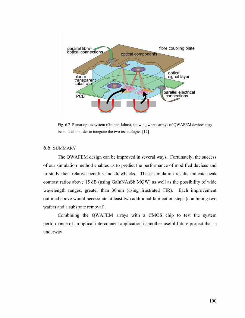
100
Fig. 6.7 Planar optics system (Gruber, Jahns), showing where arrays of QWAFEM devices may
be bonded in order to integrate the two technologies [12]
6.6 SUMMARY The QWAFEM design can be improved in several ways. Fortunately, the success
of our simulation method enables us to predict the performance of modified devices and
to study their relative benefits and drawbacks. These simulation results indicate peak
contrast ratios above 15 dB (using GaInNAsSb MQW) as well as the possibility of wide
wavelength ranges, greater than 30 nm (using frustrated TIR). Each improvement
outlined above would necessitate at least two additional fabrication steps (combining two
wafers and a substrate removal).
Combining the QWAFEM arrays with a CMOS chip to test the system
performance of an optical interconnect application is another useful future project that is
underway.
101
REFERENCES
[1] H. Q. Hou and T. Y. Chang, "Nearly chirp-free electroabsorption modulation using InGaAs-InGaAlAs-InAlAs coupled quantum wells.," IEEE Photonics Technology Letters, vol. 7, pp. 167-9, 1995.
[2] P. Steinmann, B. Borchert, and B. Stegmuller, "Asymmetric quantum wells with enhanced QCSE: modulation behaviour and application for integrated laser/modulator.," IEEE Photonics Technology Letters, vol. 9, pp. 191-3, 1997.
[3] T. H. Stievater, W. S. Rabinovich, P. G. Goetz, R. Mahon, and S. C. Binari, "A surface-normal coupled-quantum-well modulator at 1.55 mu m.," IEEE Photonics Technology Letters, vol. 16, pp. 2036-8, 2004.
[4] J. A. Trezza, M. C. Larson, S. M. Lord, and J. S. Harris, "Large, low-voltage absorption changes and absorption bistability in GaAs/AlGaAs/InGaAs asymmetric quantum wells.," Journal of Applied Physics, vol. 74, pp. 1972-8, 1993.
[5] J. A. Trezza, B. Pezeshki, M. C. Larson, S. M. Lord, and J. S. Harris, Jr., "High contrast asymmetric Fabry-Perot electro-absorption modulator with zero phase change.," Applied Physics Letters, vol. 63, pp. 452-4, 1993.
[6] J. A. Trezza, J. S. Powell, and J. S. Harris, "Zero chirp asymmetric Fabry-Perot electroabsorption modulator using coupled quantum wells.," IEEE Photonics Technology Letters, vol. 9, pp. 330-2, 1997.
[7] T. K. Woodward, J. E. Cunningham, and W. Y. Jan, "Comparison of stepped-well and square-well multiple-quantum-well optical modulators.," Journal of Applied Physics, vol. 78, pp. 1411-14, 1995.
[8] R. I. Aldaz, M. W. Wiemer, D. A. B. Miller, and J. S. Harris, "Monolithically-integrated long vertical cavity surface emitting laser incorporating a concave micromirror on a glass substrate," Optics Express, vol. 12, pp. 3967-3971, 2004.
[9] K. E. Bean, "Anisotropic etching of silicon," IEEE Transactions On Electron Devices, vol. 25, pp. 1185-1193, 1978.
[10] V. Lordi, H. B. Yuen, S. R. Bank, and J. S. Harris, "Quantum-confined Stark effect of GaInNAs(Sb) quantum wells at 1300-1600 nm.," Applied Physics Letters, vol. 85, pp. 902-4, 2004.
[11] G. A. Keeler, B. E. Nelson, D. Agarwal, C. Debaes, N. C. Helman, A. Bhatnagar, and D. A. B. Miller, "The benefits of ultrashort optical pulses in optically interconnected systems.," IEEE Journal of Selected Topics in Quantum Electronics, vol. 9, pp. 477-85, 2003.
[12] M. Gruber, R. Kerssenfischer, and J. Jahns, "Planar-integrated free-space optical fan-out module for MT-connected fiber ribbons.," Journal of Lightwave Technology, vol. 22, pp. 2218-22, 2004.
102
CHAPTER 7: CONCLUSIONS Computers and internet routers will start running up against interconnection
bottlenecks in 5-10 years (2010 – 2015). Optical interconnection systems have the
fundamental advantages to solve this problem, but will only be used if appropriate
devices can be designed to conquer both the systems requirements as well as the practical
issues.
This dissertation dealt with optoelectronic modulators for the transmitter side of
an optical interconnects implementation. The electrical system interface with CMOS
required low-voltage operation while maintaining low electrical power dissipation. The
optical communication system necessitated a high-contrast-ratio, wide-wavelength-range,
high-speed, surface-normal modulator architecture. Manufacturability and cost issues
influenced the design towards simplified fabrication techniques, a misalignment tolerant
geometry, and small size.
A surface-normal modulator was designed, fabricated, and tested in the
AlGaAs/GaAs material system for operation near 850 nm. A post-integration technique,
termed cavity tuning, was developed in order to carefully align the Fabry-Perot resonance
with the absorption spectrum of the quantum well region. This device achieved many of
the requirements laid out in Chapter 3 for an ideal modulator, but failed to modulate a
large enough wavelength range. In fact, a tradeoff between contrast ratio, wavelength
range, and voltage drive led us to abandon this architecture in favor of the more advanced
QWAFEM geometry.
The QWAFEM, a novel modulator fabricated in InGaAsP/InP for operation
around 1550 nm, satisfied all our requirements. A contrast ratio greater than 3 dB was
observed for a 16-nm-wavelength range using only 0.8-V drive for compatibility with
future CMOS digital voltage levels. To the best of our knowledge, no other surface-
normal, 1.5-µm-wavelength modulator has been developed with such performance.
Future QWAFEM designs may utilize frustrated total internal reflection (instead
of a semiconductor DBR) to generate the AFPM cavity. New quantum well materials,
such as GaInNAs(Sb)/GaAs, may also greatly improve the contrast ratio and wavelength
range. Simulations indicate wavelength ranges at least 30 nm are achievable using less
than 1-V drive.

103
To summarize, our work towards a practical optoelectronic modulator for optical
interconnects has helped us understand the challenges that optical interconnects will face
in the technical sphere as well as in the marketplace. I believe we have met those
challenges and all I can hope is that our work will either find applications in actual
systems or that it influences future modulator designers as they address their own
challenges.

104
APPENDIX A: LITHOGRAPHY PROCEDURE AND FABRICATION INSTRUCTIONS FOR ALGAAS/GAAS MODULATORS
Lithography Procedure:
(1) Solvent clean (acetone, methanol, isopropanol, water). N2 dry gently. (2) Heat for 10min at 90°C on hot plate to evaporate residual water (“singe”). (3) Spin HMDS adhesion promoter, then AZ4620 photoresist (PR). Spinner chuck should be
set at 5000rpm for 40s. (4) Remove PR from backside of wafer. (5) Bake for 10-15min at 90°C on hot plate. (6) Align on Karl Suss and expose for 36s at ~9.11 on UV lamp. (Remember to record your
exposure in the log book, including the intensity during that 36s.) While pressing the EXPOSE button, hold the microscope assembly with the other hand. It should push out to do the exposure, but it is important to keep it from jolting the entire machine, and thus misaligning the sample and mask.
(7) Develop in AZ400K developer solution for ~3.5min. (AZ400K should be diluted 1:4 in DI water, unless the bottle itself contains pre-diluted developer.)
(8) Check progress under microscope. Exposed photoresist should be removed. Any remaining PR should appear as colorful “rings” (like oil rings.) If PR is not completely removed in the appropriate areas, continue to develop and check accordingly.
1) Wafer Growth - Structure for standard p-i-n modulators, as of 10/19/00
Growth ⇓ GaAs substrate (n+ or S.I.) GaAs cleaning layer (n+) 200 Å [Si]=4.4e+18 Al0.9Ga0.1As etch stop (n+) 4250 Å [Si]=1.1e+19 GaAs (n+) 150 Å [Si]=4.4e+18 Al0.3Ga0.7As (n+) 4400 Å [Si]=4.4e+18 or higher Al0.3Ga0.7As 30 Å 50 periods of: 90 Å GaAs 30 Å Al0.3Ga0.7As Al0.3Ga0.7As (p+) 2000 Å [Be]=1.0e+19 or higher GaAs (p+) 100 Å [Be]=1.0e+19 or higher

105
2) Wafer Testing for p-i-n modulators
a) N-contacts i) Lithography (mesa positive PR, size = 3) – leaves PR to protect rectangles where mesas will
remain. To test etch calibration prior to etching full wafer, cleave a small piece and etch as below, measuring etch depth with alpha step profilometer.
ii) Wet Etch – Etch in H2SO4:H2O2:H2O (1:8:160). Calibration of this etch at room temperature is ~2200 Å/min. Etch should end in n-AlGaAs (between ~8100Å and 12500Å which implies etching for about 4.7min for the current ‘standard wafer’). It is strongly recommended to test the etch depth each time with a practice piece. Typically, we use the following procedure: (1) Draw 40mL of H2O. (2) Add 2mL of H2SO4 (sulfuric acid). Mix. (3) Draw 10.5mL of that mixture into another beaker. This should contain 10mL water and
0.5mL of sulfuric acid. (4) Add 70mL water for a total of 80mL water. Mix. Wait for the mixture to cool then add
4mL hydrogen peroxide. Mix. (5) Drop wafer in mixture for ~4.7 min. Do not stir or agitate. (6) Rinse thoroughly in DI water.
iii) Remove PR with acetone (solvent clean) and test depth with profilometer. iv) Lithography (ring contact, size = 4). v) Plasma asher for 15 seconds to descum for contacts. (<INSERT plasma asher instr>) vi) Give to Tom for deposition of n-type Ohmic contacts. Specify oxide etch (1:1 HCl/water, 15
sec, DI rinse, N2 dry) unless you are afraid of etching down right through the n+ layer. Deposit:
3000 Å Au
100 Å Ni
236 Å Au
63 Å Ge n-type ohmic contacts, no barrier
102 Å Au
108 Å Ge
substrate
vii) Liftoff – leave in acetone for >30min. Remove with bursts of acetone from solvent bottles or
“gentle ultrasound” (i.e. Little bursts). viii) Anneal about 450°C for 30 seconds. See instructions next to RTA (either in CIS or Ginzton). ix) Test n-contacts on clean room probe station using semiconductor paramter analyzer. I-V
curve should appear linear (i.e. Ohmic). b) P-contacts
i) Lithography (ring contact, size = 3) on top of mesas. ii) Plasma asher for 15 seconds to descum for contacts. iii) Give to Tom for deposition of p-type Ohmic contacts. Specify oxide etch (1:1 HCl/water, 15
sec, DI rinse, N2 dry) if you want. Deposit:
3000 Å Au
150 Å Cr p-type ohmic contacts, no barrier
substrate
iv) Liftoff (as above).

106
v) Test p-contacts and p-i-n diode structure on clean room probe station using semiconductor analyzer. I-V curve should appear linear (i.e. Ohmic) for p-to-p connections and diode-like for p-to-n connections.
c) Testing optical properties i) At the probe station, with tunable Ti:sapphire laser, check exciton peak of multiple quantum
well structure. Ideally, the lowest exciton peak (1st electron to 1st heavy hole) would appear at 850 nm. Exciton peaks ideally will not broaden much with applied voltage.
ii) Check shift of exciton peak with applied voltage between 0-6V. To do this, use the two lock-ins to measure device photocurrent and laser reference, vs. λ and vs. V. A useful Labview program in GAK’s folder on Speyside allows automation.
iii) Calculate index of refraction for each curve. Can do with the difference in absorption coefficient between your sample (which is calculated from the photocurrent measurement above) and that of bulk GaAs. A C++ program to do this Kramers-Kronig calculation is in GAK’s C++ folder.
iv) Calculate ideal voltage shift at which to operate modulator in order to maximize reflectivity (R) and change in reflectivity (DR). Can use the transfer-matrix method, such as GAK’s computer simulation. See if everything looks OK, then continue to processing.

107
3) Device Process Steps
a) N-holes (mask name: WIDE N-ETCH or N-ETCH WELLS) i) Lithography – to open up n-holes for etchant to enter. NOTE: air bubbles can remain in the
holes during etching. This screws up the etch, causing less than 100 % yield. The fix is to use water to pre-wet the wafer, i.e., spray it with the water gun for a while before trying to etch. Then put it into the etchant wet, vigorously shaking the wafer to remove the thin water film.
ii) Wet Etch – Etch in H2SO4:H2O2:H2O (1:8:160). Calibration of this etch at room temperature is ~2200 Å/min. It is safer, however, to calibrate the etch every time (on a small corner of the wafer), since the etch rate seems to vary about 20% or so. Calculate the depth of the etch for this rate. (For current wafer: Etch should end in n-AlGaAs near ~12500Å which implies etching for about 4.7min.) Use procedure outlined above for mixing the solution. Solvent clean and dry.
b) N-contacts (mask name: P-OHMIC (for p-up))
i) Lithography – makes holes for the n-ohmic deposition to stick to. Everything else lifts off. ii) Plasma asher for 15 seconds to remove PR scum. iii) Give to Tom for n-contact deposition. Assuming you want to use the p-contacts as a mirror,
don’t worry about the In barrier on top of this layer. Specify oxide etch (1:1 HCl/water, 15 sec, DI rinse, N2 dry) unless you are afraid of etching down right through the n+ layer. Deposit:
3000 Å Au
100 Å Ni
236 Å Au
63 Å Ge n-type ohmic contacts, no barrier
102 Å Au
108 Å Ge
substrate
iv) Liftoff (as above) using acetone and possibly ultrasound.
c) Anneal, Test i) Anneal using RTA, 450 ˚C, 30 seconds. Do a practice run first, since RTA often fails. ii) Test n-contacts on probe station.
d) P-contacts (mask name: N-OHMIC (for p-up)) i) Lithography – makes holes for the p-ohmic deposition to stick to. Everything else lifts off.
Since p-ohmics are not annealed, doing them after n is important, since we want to keep the reflectivity high. (This is the conventional wisdom, however, sometimes we’ve discovered that annealing p-contacts can sometimes make their ohmic character much better.)
ii) Plasma asher for 15 seconds to remove PR scum. iii) Give to Tom for reflective p-contact deposition with barrier layer. Key points: The p-contact
also acts as a reflective surface underneath the GaAs modulator. To maximize the reflectivity, we use gold as the reflective surface, and therefore skip the Cr sticking layer (which would lower R). Also, we avoid annealing the wafer after the p-contact deposition. Finally, the Indium used for flip-chip solder could alloy with the gold, again lowering the reflectivity. Therefore, we include a barrier layer, such as nickel or copper, to stop In diffusion. (Tests clearly show that gold and indium alloy into a less-reflective conductive alloy. Be sure to use the barrier wherever you care about reflectivity.)
2000 Å Au

108
500 Å Cu p-type ohmic contacts, with In diffusion barrier
2000 Å Au
substrate
iv) Liftoff (as above) using acetone and possibly ultrasound. v) Test electrical characteristics.
e) Capacitance Reduction (mask name: P-ETCH WELLS)
i) Lithography – opens up the p-contact area in order to etch off the p-region everywhere except where the contact itself is. The contact itself protects the region below it, since we use an anisotropic dry etch. This reduces the capacitance of the devices significantly.
ii) Bring to CIS clean room. Affix sample to carrier wafer with a small piece of copper tape that ends up completely concealed by the sample. (ie. No copper tape showing…) This tape removes the requirement for a PR hard bake step and the resultant difficulty in removing that PR.
iii) PlasmaQuest (see (g) below…) through the p-region. Always calibrate Pquest before doing it on your actual samples.
f) Mesa Etch (mask name: MESA ETCH)
i) Lithography – covers both contacts and significant surrounding area. We etch away everything else, down beyond the etch stop layer. Thus, following substrate removal, only the mesas will remain on the chip.
ii) Use copper tape. Hardbake – important! To avoid burning the photoresist in the PlasmaQuest, we do a photoresist hardbake after developing. Using a hotplate, bake the PR mesas at 140°C for 30 minutes.
iii) Dry etching with PlasmaQuest in CIS clean room. Use anisotropic dry etch for GaAs/AlGaAs using BCl3 and Cl2 as the active etchants and significant RF power for straight side-walls. The recipe titled “gordona1” is likely the latest and greatest version. One recipe that works: 400 W ECR, 10 W RF 10 sccm Ar, 15 sccm BCl3 , and 1 sccm Cl2
(HC: Actually, stored recipe parameters are 15, 10, 3. Typically, actual measured numbers during run are 14, 10, 1.5)
Etch rate of roughly 0.17 µm/min means a 15 minute etch (900 sec) will etch about 2.5 microns, sufficient for an average wafer.
iv) Photoresist stripping – this step takes more time because of the hardbake and plasma etching. Acetone alone will not work. Instead, use 1165 photoresist remover, a.k.a. N-methyl-2-pyrrolidone. Remove the resist in a covered beaker of 1165 at 65°C for 60 minutes. Key: you must give the beaker several seconds (~10 sec) of ultrasound agitation a few times during the hour soak. This removes those hangy bits around the mesa edges. A plasma ashing at the end may also prove quite helpful. (Oftentimes, we have seen 1165 overnight soaking be insufficient, but a few minutes in the plamsa asher cleans it off beautifully.)]]
g) Indium Deposition (mask name: NP CONTACTS #2 (bigger holes))
i) Lithography – opens both contacts for indium solder bumps. Everything else lifts off. ii) Bring to CISX. See additional procedure on indium evaporation. Deposit 3-6 microns of In. iii) Liftoff.
h) Array Protection (mask name: ARRAY PROT)
i) To avoid covering up the wire bonding pads on the CMOS chip, we must remove the arrays of devices that surround the central array of devices. This can be done using a large photoresist square to protect the main array. Use the quarter of the mask that has ~1.5mm solid squares. Also, overexpose the resist, because it is likely to be extra thick at the edges and in between unwanted mesas. (i.e., 1813 with 40 second exposure, or 4620 with 45 seconds)
ii) Etch away the unwanted stuff. Sulfuric acid:hydrogen peroxide:water (1:8:1) for 1 minute.

109
iii) Solvent clean to remove the photoresist. iv) Look under the microscope. The removed devices will still be somewhat visible as little
pyramids. Contrast the actual devices and removed devices to be sure they are completely gone.
i) Cleave modulator arrays
i) Choose to cleave through the array directly next to the desired array (leaving about a 2mm by 2mm square of GaAs) or through the next array (for a 5mm by 5mm array).
ii) This step may be done at any time, possibly during steps f), g) or h). Key points: photoresist (especially hardbaked photoresist) will protect the indium bumps during handling, so cleaving while covered with photoresist may be smart. Spinning is annoying on many small chips, so waiting to cleave near the end is also a good plan.
iii) To cleave without damaging devices, hold the wafer by its edges with tweezers. Working on a microscope slide is helpful. Carefully scribe through an array at an edge. Now hold the scribe line over the edge of the slide and use the scribe tip to push down on the GaAs bit (on something unimportant)… Other scribing methods work equally well or better. Harris Group students tend to scribe along the edge, then press vertically with the scribe tip on that spot. We have not tried that yet.
j) Prepare Si/CMOS chips – gold on Al pads (mask name: FLIPCHIPG1, I think)
i) Lithography – to open holes for Au deposition. Indium will stick better to gold, but Al and Au will mix to form a non-conductive ‘purple plague’. Make sure to deposit a barrier layer. (1) Clean and prebake the CMOS to dry it. (2) Spinning PR will be complicated due to the fact that the huge edge bead will impede the
exposure, due to the small size of the chips (2mm x 2mm). To compensate: (3) Spin PR thin onto a glass slide piece to be used as “glue”. A few drops of AZ4620
@1000 rpm, 40 seconds is pretty good. (4) Place Si/CMOS chip in center of PR as flat as possible. (5) Tile the surrounding area with square pieces of blank Si, such that all
edges of the Si/CMOS chip are touching a piece of blank Si. This will allow the edge bead to form completely on the blank Si pieces, and not on the center Si/CMOS chip, which is all we care about.
(6) Bake the whole mess for ~110 sec @ 90°C to firm it up for spinning. (7) Spin on as in standard lithography, then remove Si pieces by pushing them away from the
chip (or tangentially from it) with tweezers. The CMOS may come off too, but it can be stuck down to another cover slip. Now do the standard lithography post-bake.
(8) Alignment technique – You must try to align the CMOS chip rotationally and in the y-direction by looking through an open part of the mask next to the pad array. Then, using a high-power objective, look through the tiny pad holes and count the 20 Aluminum pads go past on the CMOS chip (see below).
(9) Overdevelop (~0.7-0.8 min) in case the PR was extra thick.

110
(10) There is a good chance that an edge bead will be too soft, stick to the mask, and pull off. This exposes the CMOS pads, which could be disastrous if they get shorted by the metallization. Cover these spots by dabbing on some partly-dried up PR from the spinning process. Use the tips of a sharp pair of tweezers, and be careful not to mess up the rest of the chip.
(11) Overbake (20-25 min) the whole thing a bit to harden the PR “glue” under your chip, which will otherwise bubble and make Tom upset.
Continue with standard lithography procedure: ii) Plasma asher for 15 seconds to descum PR. iii) Give to Tom for gold deposition with barrier layer. Specify oxide etch (1:1 HCl/water, 15 sec,
DI rinse, N2 dry). Deposit:
3000 Å Au
1000 Å Cu CMOS contacts, with Al diffusion barrier
150 Å Cr
substrate
align here
CMOS

111
4) Flip-Chip Bonding
a) Flip Chip Bond at CIS. See additional procedure on flip-chip bonding process. We have been told (by Lucent & Opticomp) that using a bonding pressure (mass) of 0.5 - 1 gram/bump is best for these indium bumps. We have tried from 0.5-4.0 grams though, and it is unclear what is actually best. They also recommended times as short as 1 second, although we currently use longer times (approximately 1 minute). More recently, we’ve had success (ie. Better mechanical stability, equivalent yield electrically) doing 2 g/bump (ie. 800g / array) and raising the temperature up to 150C for 30 s or so, while applying pressure the whole time.
b) Wick in epoxy. This provides additional mechanical strength for the modulators after substrate removal, and stops any wet etchants from attacking the modulators from the side during substrate removal (and protects the CMOS – key point: the Al pads will be etched by almost any acid). The current epoxy type is TRA-BOND BA-2113: i) Mix epoxy. Try to avoid introducing any bubbles. The best way is to skip the mixing
container altogether. Instead, cut both ends of the tube and squeeze it into a small disposable dish, stirring gently.
ii) Apply dabs to edge of Si/GaAs interface. The best way we’ve tried is to dip about 1 cm of a glass fiber into the epoxy and let it run down in a small bead. Be careful not to get epoxy on either the GaAs back surface, or on the microscope slide during the curing process (or you will never get the chip off!) Applying the epoxy while the chip sits on a cover slip is not a bad idea. It is, of course, important to make sure that the GaAs side does not get epoxied at all.
iii) Cure for 4 hours at 65°C (or longer to ensure complete hardness), or 24 hours at room temp. 5) Substrate Removal – new and improved!
a) Non-selective removal. This is a fast wet etch to remove most of the substrate, leaving about 50µm to remove selectively. Use H2SO4:H2O2:H2O (1:8:1) for crazy-fast etching (5mm/min). Make sure it cools first. About 30 minutes in here tears through a lot of substrate. (Note: it seems to matter if the GaAs is bigger than the Si CMOS or vice versa. When the GaAs wafer piece is larger, 30-45 minutes is good in the fast wet etch. When the Si is larger, it usually requires about 60-70 minutes.) HC: Currently, we use photoresist to stick small chip pieces onto larger glass slides. Then we can put these larger pieces into a basket without the pieces falling through the holes. Put the basket into a tall beaker with a magnetic stir-bar; the basket rests on top of a plastic spacer to leave room for the stir-bar. Vigorously stir the etchant. This seems to make the GaAs etch more uniformly at a fairly consistent rate of 10 microns/minute. Periodically measure the thickness with the thickness-measurer in the clean room. When there is about 100 microns left, go another 5 minutes and then stop. Don’t use the thickness-measurer if there is less than 100 microns left, in case the GaAs breaks.
b) Selective etch. This should stop on the AlGaAs etch stop layer, leaving the modulators behind on the CMOS. Use Citric Acid:Hydrogen Peroxide (4:1). This etch is supposed to be 1000 times selective in etching GaAs over AlGaAs. Actual etch rates from papers:
- GaAs, ~4000 Å/min - AlAs, ~1 Å/sec - Al.60Ga.40As, ~5-10 Å/sec (from our experience)
(1) If you have no citric acid, it is prepared from 1 part anhydrous citric acid to 1 part water. A bottle should last for a year or something. Mixing takes a while (a day or so).
(2) Prepare the citric/peroxide mixture and be sure to stir it well. (3) Do a 1:1 HCl/water dip for 60 seconds, DI water dip for 30 seconds, touch to wipers to
dry but don’t blow dry! (An oxide layer will completely stop the citric acid etch from working.)
(4) Etch until you hit the etch stop. Stop. If you are impatient, you can heat the citric acid mixture to 60C on a hot plate while it’s etching. This significantly improves the etch rate

112
of GaAs, and the selectivity is generally good enough, if your etchstop is reasonably thick. Key point: If you heat the citric acid, make sure not to change the temperature of any given chip too rapidly, or the GaAs can fracture, especially if it is thin. For example, do not take it out of the hot citric and throw it into a bath of cold water. HC: Recently, we have been heating the citric to 40C. This seems to etch the GaAs at about 1 micron/minute. Check the chips every 3 minutes when you’re close: otherwise the etch stop will also be removed.
(5) Remove the etch stop. The formula that seems to succeed with our 90% Al etch stop is the following: (a) HCl:water for 90 s. You should watch carefully to see the colors change. (Often we
have seen it change from red-green-red-green-gray-gray-gray-gray… then it’s done.) d) After this, we expect you can tune the thickness of the device by doing successive H2O2 and
HCl/water dips, which should remove about 10-20 Å/cycle of GaAs and also smooths the surface. Experimentally, we have seen a shift of the Fabry-Perot peak after these dips. In order to see this, we had to scan the reflectivity using the probe station after each series of dips. Be sure to use clean water each time – contamination of the water due to a small amount of HCl and H202 can cause slow etching, ruining the precision of this technique. (If it is useful to remove epoxy first, that can be done, but this allows tuning etchants to attack the sides of the devices. Use NH4OH:H2O (1:9) instead of HCl:water (1:1) since it should not attack the AlGaAs or GaAs.) In the end, you should do a 5-30 sec dip in peroxide, rinse in clean water, dry with nitrogen, then a 5-30 sec dip in oxide-etcher (HCl or NH4OH based), rinse in clean water (not the same bucket!), dry with nitrogen. Repeat ad nauseum. Wavelength shifts about ¾ nm per cycle.
e) Epoxy removal. Use Phlegmatron plasma asher in Ginzton. This step is necessary to remove the epoxy from on top of the CMOS wire bonding pads. Lately, this has been less than easy. Using process #5, set the Gas 1 at 83% and Gas 2 at 17%. Set RF power = 25%. About 30 minutes should be sufficient, but it seems that overheating causes the epoxy to burn, turning it a bit crispy-looking. Place chips on top of a bunch of glass slides. It seems that removing the epoxy redeposits some crap around nearby. If the plasma asher fails to pump down below, say, 700 mtorr, chances are good that some epoxy crap remains inside the chamber and is keeping it from pumping by outgassing. The solution, kind of, is to wipe down the asher chamber with isopropanol and try to pump down again. If it fails, repeat. Eventually, this seems to work. In this case, when the asher fails to rough down far enough, press the blue POWER button and vent the chamber by reaching your arm (carefully) into the back of the asher and turning that cute green valve, near the hydraulic column that raises the roof. You should hear a pleasant hissing sound that dissipates as the chamber comes to 1 atm. Close that valve. Now you can open it up and wipe it down again… HC: Also, you can use drytek4 in CIS. Look up past log entries by Henry Chin. Parameters: 4sccm CHF3, 20 sccm (i.e. 100%) O2, Pressure = 150mtorr, RF = 100 W forward / 0 W reverse. Go 5 minutes at a time to prevent overheating.
6) Test the Chip

113
APPENDIX B : MATLAB SIMULATION CODE FOR QWAFEM
This appendix contains code for the transfer matrix method simulation. This code is written in MATLAB format. The main piece of code (opt_tmm_main.m) has been edited to include only a single mode of operation, for the sake of brevity. This mode calculates the reflectivity of the design as a function of wavelength for two different voltages. It can use this information to display plots of the reflectivity, contrast ratio, and change in reflectivity (∆R). Several other modes were developed for optimizing aspects of the design, but are omitted below for space reasons. The full code can be obtained by contacting the Miller Group. % ===================================================================== % opt_tmm_main.m % Noah Helman % 12 Dec 2002 % 28 Aug 2003 -- updated with proper amplitude_thetaj formula... and other things... % Algorithm: % - Load all relevant information. define_params; if summarymode == 0 & optimizationmode <= 0 clear R_TE R_TM disp('Calculating R_TE vs wavelength for Gaussian beams -- please be patient...'); for field = low:high for wave=1:length(activelow(1,:)) maxlayer = length(layerd); wavelength = 1e-9*activelow(1,wave); omega = 2*pi*c/wavelength; thetaj_norm = 0; thetaj_count = 1; R_TE_wave = 0; for thetaj = thetaj_start:thetaj_step:thetaj_stop tmm_calc_TE; thetaj_count = thetaj_count + 1; R_TE_angle = (abs(S_TE(2,1))*abs(S_TE(2,1))) / (abs(S_TE(1,1))*abs(S_TE(1,1))); T_TE_angle = 1/(abs(S_TE(1,1))*abs(S_TE(1,1))); amplitude_thetaj = exp( (-(thetaj - thetaj_center)^2)/( (wavelength/(pi*w0*n_inp)).^2)); thetaj_norm = thetaj_norm + amplitude_thetaj^2; R_TE_angle = R_TE_angle * amplitude_thetaj^2; R_TE_angle_vector(thetaj_count-1) = R_TE_angle; amplitude_vector(thetaj_count-1) = amplitude_thetaj^2;

114
R_TE_wave = R_TE_wave + R_TE_angle; end % thetaj if field == low R_TE_low(wave) = R_TE_wave/thetaj_norm; R_TE_low_fiber(wave) = sum(R_TE_angle_vector.*amplitude_vector./thetaj_norm); else R_TE_high(wave) = R_TE_wave/thetaj_norm; R_TE_high_fiber(wave) = sum(R_TE_angle_vector.*amplitude_vector./thetaj_norm); end; end; %wave end; %field CR = R_TE_low./R_TE_high; dR = R_TE_low - R_TE_high; CRfiber = R_TE_low_fiber./R_TE_high_fiber; dRfiber = R_TE_low_fiber - R_TE_high_fiber; dl = wavelength_axis(2) - wavelength_axis(1); [maxCR,iCR] = max(CR); [maxdR,idR] = max(dR); sprintf('Max CR = %0.3f at %d nm',maxCR, wavelength_axis(iCR)) sprintf('Max dR = %0.3f at %d nm',maxdR, wavelength_axis(idR)) sprintf('Size of wavelength range where CR is greater than two: %d nm',dl*sum(CR>2)) % ======================================================================== % % define_params.m % % % Noah Helman % April 2003 updated % August 2003 updated % % Includes all parameters of the simulation to be done. Examples are constants % such as the index of refraction of gold and also user defined parameters such % as the optical structure to be simulated. % clear; % CONSTANTS: % overall: low = 1; high = 2; c = 3e8; % indices of refraction:

115
n_air = 1; n_gold = 0.252-5.4*i; % from Palik for 886 nm n_gold = 0.38-10.75*i; % from Luxpop.com for 1550nm n_inp = 3.163; n_ti = 3.69-4.62*i; % from luxpop.com at 1550nm % beam waist minimum radius inside the InP material (?!) w0 = 10e-6; %w0 = 10e-6; operating_wavelength = 1.506e-6; % facet angle: thetaf = 54.7 * (pi/180); % crossing half-angle: theta = 2*thetaf - pi/2; %theta = 30*pi/180; theta = pi/2; % surface normal % transfer matrix paramters: % Gaussian parameters num_angles = 35; % <===should be an odd number; thetaj_center = pi/2 - theta; % thetaj_step = operating_wavelength/(w0*pi*n_inp); thetaj_step = pi/800; thetaj_step = pi/1600; % thetaj_step = thetaj_step/2; thetaj_start = thetaj_center - thetaj_step * ( (num_angles-1)/2 ); thetaj_stop = thetaj_center + thetaj_step * ( (num_angles-1)/2 ); % electric field: field = high; %field = low; % DEFINE STRUCTURE: % Rules: % - layerd defines the thicknesses (in nm). % - layertype defines the type of material: % 1 = air % 2 = gold % 3 = active layer (changes high/low) % 4 = user defined constant % 5 = from an equation (uses n_user to adjust by certain amounts) clear layerd layertype n_user clear layerd_mqw layertype_mqw n_user_mqw clear layerd_oepic layertype_oepic n_user_oepic clear layerd_test layertype_test n_user_test % Tips on designing a structure: % - put the 'bottom' layer, optically, at the end, such as a gold reflective layer. % for the oepic device this results in n_inp-ingaaspMQW-p_inp-air-- % - put some air as the very last layer on the right. % - during the plots, the last air layer will not show up. Omlw2792 = 1;

116
layerd_opt =[ 3000 42 354 222 278 227 233 122 93 20 50 200 200]; layertype_opt =[ 6 5 6 5 6 5 6 3 6 4 6 1 1 ]; n_user_opt =[ n_inp nq n_inp nq n_inp nq n_inp 0 n_inp ncap n_inp 0 0 ]; % ========================================================================== if omlw2792 == 1 layerd = layerd_opt; layertype = layertype_opt; n_user = n_user_opt; active_low_file = 'kk3Files\m2793_kk3_AR_fix_1.txt'; % the "fix" files have an opposite sign in the active_high_file = 'kk3Files\m2793_kk3_AR_fix_5.txt';
% KK3 part of the MQW n... giving same look as GAK's GaAs data end [fid, message] = fopen(active_low_file, 'r'); disp(message); activelow=fscanf(fid, '%f', [3,inf]); fclose(fid); [fid, message] = fopen(active_high_file, 'r'); disp(message); activehigh=fscanf(fid, '%f', [3,inf]); fclose(fid); alpha_adjust = 1; %0.86; %******************************************************************* n_low = activelow(3,:)-i*(alpha_adjust.*activelow(1,:).*activelow(2,:)*1e-7/(4*pi)); n_high = activehigh(3,:)-i*(alpha_adjust.*activehigh(1,:).*activehigh(2,:)*1e-7/(4*pi)); wavelength_axis = activelow(1,:); % CONSTRUCT N MATRIX % % The inputs to the n() matrix are: % - wavelength marker (an index that is 1-to-1 linked to lambda) % - low/high mode % - layer number j wavepoints = size(activelow,2); for j=1:length(layerd) if layertype(j) == 1 for p=1:wavepoints n(p,low,j) = n_air; end; elseif layertype(j) == 2 for p=1:wavepoints n(p,low,j) = n_gold; end; elseif layertype(j) == 4 for p=1:wavepoints n(p,low,j) = n_user(j); end elseif layertype(j) == 5

117
% *** using equation derived from ellipsometry of InGaAsP (1.38Q) by Virginia Robbins at Agilent % center value might be different but slope is similar in all measurements. nqk_slope = -5.37067e-05; nqk_intercept = 0.094735598; % nqk_slope = 0; % nqk_intercept = 0.010; % n(:,low,j) = wavelength_axis * nq_slope + nq_intercept; n(:,low,j) = wavelength_axis * (nq_slope-i*nqk_slope) + nq_intercept - i*nqk_intercept; elseif layertype(j) == 6 % *** using equation derived from ellipsometry of InP:S by Virginia Robbins at Agilent % center value might be different but slope is similar in all measurements. % assuming 15A oxide thickness, you get the following for the index with almost 0 for absorption... n_inp_slope = -0.000131; n_inp_intercept = 3.3356 + 0.05; % n_inp_k = -0.0000; % n(:,low,j) = wavelength_axis * nq_slope + nq_intercept; n(:,low,j) = wavelength_axis * n_inp_slope + n_inp_intercept + i*n_inp_k; elseif layertype(j) == 3 nq_slope = -0.000203; nq_intercept = 3.723; n(:,low,j) = n_low - 3.55 + wavelength_axis * nq_slope + nq_intercept; n(:,high,j) = n_high - 3.55 + wavelength_axis * nq_slope + nq_intercept; end % fill in matrix elements, equating hi/lo columns for nonactive layers if layertype(j) ~= 3 n(:,high,j) = n(:,low,j); end; end; % summary mode: % in summary mode, the program will only calculate all angles for the operating % wavelength, and will only calculate the center angle. it looks ugly, but it works. % 0 = calculate R vs lambda for all angles, all wavelengths % 1 = calculate only center angle (thetaj_center) for all wavelengths except operating_wavelength % 2 = calculate only operating wavelength % 3 = print out the low and high absorption coefficients summarymode = 0; % optimizationmode: % in optimization mode, the program changes a parameter in order to optimize some result.

118
% 0 = do not vary anything. run in summarymode. % 1 = vary thickness of certain layer (stored in layervary) in num_steps of layerd_step % around the original thickness. % 2 = vary the facet angle between 46 and 55 degrees roughly. % 3 = vary the index of refraction of the MQW region(s). % 4 = vary the width of the optical beam at its focus (w0) % 5 = vary the thickness of two layers below. % 6 = growth error tolerance checker % 7 = vary the absorption coefficient of one layer. optimizationmode = 0; switch optimizationmode case {1} % optimizationmode == 1 parameters: layervary = 2; num_steps = 51; % should be an ODD number. layerd_step = 5; % thickness variation will be equal to num_steps * layerd_step... layervary_thin = layerd(layervary) - ( (num_steps - 1)/2)*layerd_step; layervary_thick = layerd(layervary) + ( (num_steps - 1)/2)*layerd_step; layervary_axis = [layervary_thin:layerd_step:layervary_thick]; layervary_orig = layerd(layervary); case {2} % optimization == 2 parameters: clear thetafv; thetafstart = 46 *pi/180; thetafstep = pi/(180* 2 ); thetafstop = 86.5 *pi/180; thetafv = [thetafstart:thetafstep:thetafstop]; case {3} % optimization mode 3 parameters: nteststep = .0005*i; ntestnum = 40; nteststart = - ntestnum*nteststep; nteststop = + ntestnum*nteststep; layervary3 = [2 4 6]; case {4} % optimization mode 4 parameters: w0_min = 2e-6; w0_max = 60e-6; w0_step = 2e-6; case {5} % optimization mode 5 parameters: layervary1 = 2; num_steps1 = 31; % should be an ODD number. layerd_step1 = 4; % thickness variation will be equal to num_steps * layerd_step... layervary2 = 4; num_steps2 = 23; % should be an ODD number. layerd_step2 = 4; % thickness variation will be equal to num_steps * layerd_step... layervary_thin1 = layerd(layervary1) - ( (num_steps1 - 1)/2)*layerd_step1; layervary_thick1 = layerd(layervary1) + ( (num_steps1 - 1)/2)*layerd_step1; layervary_axis1 = [layervary_thin1:layerd_step1:layervary_thick1];
119
layervary_orig1 = layerd(layervary1); layervary_thin2 = layerd(layervary2) - ( (num_steps2 - 1)/2)*layerd_step2; layervary_thick2 = layerd(layervary2) + ( (num_steps2 - 1)/2)*layerd_step2; layervary_axis2 = [layervary_thin2:layerd_step2:layervary_thick2]; layervary_orig2 = layerd(layervary2); case {7} % optimizationmode 7 parameters: layervary = 8; num_steps = 51; astep = 100; % inverse cm... end calc_fields = 0; interfacephase = 0; asintest = 0; %17; versionnumber = version('-release'); % returns a string like '12'; P_in = 5.7; %uW -- measured value of 5.7uW corresponds to 100uW out of laser, internally chopped. Pchip = P_in * (1-( (n_inp - 1)/(n_inp + 1))^2); Resp = 1.24; %A/W substrateloss = .15; %percent on single pass loss factor... % PLOTTING PARAMETERS ================= dz = 15; % nm dx = 800; % nm x_count_max = 75; layermarkers = 1; % ========================================================================== % plot_opt_tmm.m % Noah Helman % 12 Dec 2002 % Plots results of opt_tmm_main. disp('plotting results'); disp('summarymode = '); disp(summarymode); disp('optimizationmode = '); disp(optimizationmode); if summarymode <= 1 & optimizationmode == 0 % PLOT results figure(1) hold off plot(wavelength_axis, R_TE_low); hold on plot(wavelength_axis, R_TE_high, 'g'); xlabel('wavelength (nm)'); ylabel('reflectivity'); title('QWAFEM reflectivity'); axis([wavelength_axis(1) max(wavelength_axis) 0 1]);

120
figure(2) hold off plot(wavelength_axis, CR); hold on plot(wavelength_axis, CRfiber, 'g'); xlabel('wavelength (nm)'); ylabel('contrast ratio'); title('Contrast ratio for free space (blue) and fiber coupled (green)'); figure(3) hold off plot(wavelength_axis, dR); hold on plot(wavelength_axis, dRfiber, 'g'); xlabel('wavelength (nm)'); ylabel('change in reflectivity dR'); title('Change in reflectivity for free space (blue) and fiber coupled (green)'); figure(8) hold off plot(wavelength_axis, PC_TE_low); hold on plot(wavelength_axis, PC_TE_high, 'g'); xlabel('wavelength (nm)'); ylabel('photocurrent (au)'); title('photocurrent spectra'); figure(1) end % ====================================================================== % make_E_zz.m % Noah Helman % 12 Dec 2002 % Creates E-field as a function of spatial coordinates z (growth) direction. % Takes as inputs a lot of things: % - all the stuff in define_params.m % - wave, thetaj % - layerd (which changes during optimizationmode) for zz = dz:dz:layerd(layeri) P_TE_zz = [exp(i*p_i_k*zz) 0; 0 exp(-i*p_i_k*zz)]; S_TE_zz = P_TE_zz * S_TE; zz_axis(count) = sumlayerd + zz; Einc_zz(count) = S_TE_zz(1,1); Eref_zz(count) = S_TE_zz(2,1); count = count+ 1; end sumlayerd = sumlayerd + layerd(layeri); for a=1:length(Einc_zz)

121
Einc_TE(wave,a) = Einc_zz(a); Eref_TE(wave,a) = Eref_zz(a); end % ====================================================================== % make_E_xz.m % Noah Helman % 12 Dec 2002 % Creates E-field as a function of spatial coordinates x (lateral) and z (growth) directions. % Takes as inputs a lot of things: % - all the stuff in define_params.m % - wave, thetaj % - layerd (which changes during optimizationmode) clear Einc_TE_xz Eref_TE_xz %clear Einc_TE_xz_all Eref_TE_xz_all for x_count=1:2*x_count_max+1 x_location = (x_count - x_count_max - 1); xx_axis(x_count) = x_location * dx; Einc_TE_xz(x_count, :) = Einc_TE(wave, :) * exp(i*beta0*x_location*dx*1e-9); Eref_TE_xz(x_count, :) = Eref_TE(wave, :) * exp(i*beta0*x_location*dx*1e-9); end % fudge here: the n_inp in the following line is not strictly correct, i guess... amplitude_thetaj = exp( (-(thetaj - thetaj_center)^2)/( (wavelength/(pi*w0*n_inp)).^2)); %thetaj_norm = thetaj_norm + amplitude_thetaj; %R_TE_angle = (abs(S_TE(2,1))*abs(S_TE(2,1))) / (abs(S_TE(1,1))*abs(S_TE(1,1))); if thetaj_count == 1 Einc_TE_xz_all = amplitude_thetaj * Einc_TE_xz; Eref_TE_xz_all = amplitude_thetaj * Eref_TE_xz; % R_TE(wave) = amplitude_thetaj^2 * R_TE_angle; else Einc_TE_xz_all = Einc_TE_xz_all + amplitude_thetaj * Einc_TE_xz; Eref_TE_xz_all = Eref_TE_xz_all + amplitude_thetaj * Eref_TE_xz; % R_TE(wave) = R_TE(wave) + amplitude_thetaj^2 * R_TE_angle; end % ========================================================================= % tmm_calc.m % Noah Helman % 12 Dec 2002 % reorganized subprocedure to do just the tmm part of the calculation. % assumes lots of things as inputs: % - all the stuff in define_params.m % - wave, thetaj % - layerd (which changes during optimizationmode) %calculate k_x0 = beta0; the vacuum wavevector. Then beta = beta0*n_i for i-th layer. % DO WE NEED TO USE SNELL'S LAW TO CALC theta EACH TIME IN EACH LAYER??? % beta should be the same in EVERY LAYER. Therefore, we can set it once as beta0

122
% in the following line and be done with it. Snell's law is included. % NOTE: this assumes that the angles thetaj are defined as inside the InP % substrate. they are not free space angles, though 'wavelength' is % the free space wavelength. n1 = n(wave,field, 1); beta0 = 2*pi*n1*sin(thetaj)/wavelength; S_TE = eye(2); S_TM = eye(2); sumlayerd = 0; count = 1; %clear zz_axis Einc_zz Eref_zz; % transfer matrix calculation. % plane wave of specific wavelength and angle. % at a particular value of x... for layeri = (maxlayer-1):-1:1 ni = n(wave,field,layeri); nii = n(wave,field,layeri+1); n1 = n(wave,field, 1); % TE polarized light: neff_i_TE = ni * sqrt(1-((c*beta0)/(omega*ni ))^2); neff_ii_TE = nii* sqrt(1-((c*beta0)/(omega*nii))^2); % *** Must choose the sign of the sqrt properly to get correct phases % on reflection! *** if imag(neff_i_TE) > 0 neff_i_TE = conj(neff_i_TE); end if imag(neff_ii_TE) > 0 neff_ii_TE = conj(neff_ii_TE); end % ********* tested for release 12 and 13 and works for both for TE. r_i_TE = (neff_i_TE - neff_ii_TE)/(neff_i_TE + neff_ii_TE); t_i_TE = 2*neff_i_TE/(neff_i_TE + neff_ii_TE); % IS THE PHASE CHANGE ON REFLECTION FOR TE FOR TIR POSITIVE OR NEGATIVE???? % positive! according to these new formulae and Hecht. if interfacephase == 17 theta_i = asin(n1*sin(thetaj)/ni); theta_ii = asin(n1*sin(thetaj)/nii); if asintest == 17 & versionnumber == '12' theta_i; theta_ii; end %[s,e]= sprintf('thetas are %0.1f and %0.1f\n', theta_i*180/pi, theta_ii*180/pi); %disp(s); r_i_TE = (ni*cos(theta_i) - nii*cos(theta_ii))/(ni*cos(theta_i) + nii*cos(theta_ii)); t_i_TE = 2*ni*cos(theta_i)/(ni*cos(theta_i) + nii*cos(theta_ii)); end
123
if asintest == 17 sprintf('ni = %f and nii = %f\n', ni, nii) sprintf('phase of r_i_TE is %f\n', angle(r_i_TE)*180/pi) end D_TE = (1/t_i_TE)*[1 r_i_TE; r_i_TE 1]; p_i_k = (1e-9)*sqrt( (omega*ni/c)^2 - beta0^2); if imag(p_i_k) > 0 p_i_k = -1 * p_i_k; % p_i_k = conj(p_i_k); %<=== this gives wrong answers normal incidence... end P_TE = [exp(i*p_i_k*layerd(layeri)) 0 ; 0 exp(-i*p_i_k*layerd(layeri))]; S_TE = D_TE * S_TE; % calculate the E-field in different locations in this layer: if (summarymode >=2)|(calc_fields == 1) make_E_zz; end % Finally, calculate the S matrix for the entire layer... S_TE = P_TE * S_TE; end %layeri
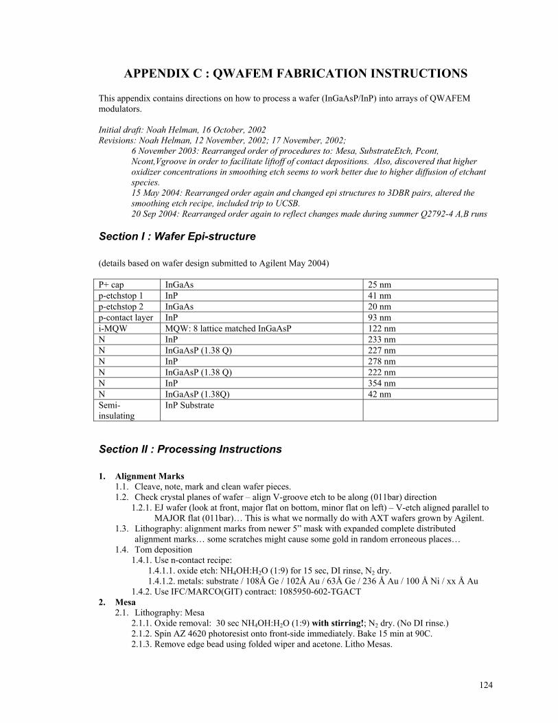
124
APPENDIX C : QWAFEM FABRICATION INSTRUCTIONS This appendix contains directions on how to process a wafer (InGaAsP/InP) into arrays of QWAFEM modulators. Initial draft: Noah Helman, 16 October, 2002 Revisions: Noah Helman, 12 November, 2002; 17 November, 2002;
6 November 2003: Rearranged order of procedures to: Mesa, SubstrateEtch, Pcont, Ncont,Vgroove in order to facilitate liftoff of contact depositions. Also, discovered that higher oxidizer concentrations in smoothing etch seems to work better due to higher diffusion of etchant species. 15 May 2004: Rearranged order again and changed epi structures to 3DBR pairs, altered the smoothing etch recipe, included trip to UCSB. 20 Sep 2004: Rearranged order again to reflect changes made during summer Q2792-4 A,B runs
Section I : Wafer Epi-structure (details based on wafer design submitted to Agilent May 2004) P+ cap InGaAs 25 nm p-etchstop 1 InP 41 nm p-etchstop 2 InGaAs 20 nm p-contact layer InP 93 nm i-MQW MQW: 8 lattice matched InGaAsP 122 nm N InP 233 nm N InGaAsP (1.38 Q) 227 nm N InP 278 nm N InGaAsP (1.38 Q) 222 nm N InP 354 nm N InGaAsP (1.38Q) 42 nm Semi-insulating
InP Substrate
Section II : Processing Instructions 1. Alignment Marks
1.1. Cleave, note, mark and clean wafer pieces. 1.2. Check crystal planes of wafer – align V-groove etch to be along (011bar) direction
1.2.1. EJ wafer (look at front, major flat on bottom, minor flat on left) – V-etch aligned parallel to MAJOR flat (011bar)… This is what we normally do with AXT wafers grown by Agilent.
1.3. Lithography: alignment marks from newer 5” mask with expanded complete distributed alignment marks… some scratches might cause some gold in random erroneous places…
1.4. Tom deposition 1.4.1. Use n-contact recipe:
1.4.1.1. oxide etch: NH4OH:H2O (1:9) for 15 sec, DI rinse, N2 dry. 1.4.1.2. metals: substrate / 108Å Ge / 102Å Au / 63Å Ge / 236 Å Au / 100 Å Ni / xx Å Au
1.4.2. Use IFC/MARCO(GIT) contract: 1085950-602-TGACT 2. Mesa
2.1. Lithography: Mesa 2.1.1. Oxide removal: 30 sec NH4OH:H2O (1:9) with stirring!; N2 dry. (No DI rinse.) 2.1.2. Spin AZ 4620 photoresist onto front-side immediately. Bake 15 min at 90C. 2.1.3. Remove edge bead using folded wiper and acetone. Litho Mesas.

125
2.2. Etch: Mesa 2.2.1. Before etching: ALWAYS protect wafer backside with 1805 PR painted. 2.2.2. Be sure to test the etch on a test piece every time. 2.2.3. 5 sec Sulfuric:Peroxide:Water (1:2:10) -- to etch p+ cap. Etches 100 nm/min. 2.2.4. 5 sec Hydrochloric Acid – to etch p-InP. Etches 5 µm/min. Repeat last two steps to etch
down to i-MQW region. 2.2.5. 1-2 min Sulfuric:Peroxide:Water (1:2:10) -- to etch InGaAsP MQW region 2.2.6. Dip in HCL to see if bubbles appear showing that the MQW region is gone and n-InP was
etched… measure in alphastep profilometer. 3. N-contact
3.1. Lithography: N-contact with edge bead removal technique 3.2. Tom dep: oxide etch + substrate / 108Å Ge / 102Å Au / 63Å Ge / 236 Å Au / 100 Å Ni / xx Å Au 3.3. Liftoff in acetone (5min soak, then spray off, then use ultrasound, if necessary…).
4. Substrate etch 4.1. Deposit 500 nm SiO2 on wafers using STS PECVD at SNF. (recipe=nch_sio2) 4.2. Lithography: n-etch with edge bead removal technique. 4.3. Etch into SiO2 using drytek4 (CHF3 (100 sccm) and O2 (5 sccm (25%)) for around 35min in 5-10
min steps). Look at old recipes, if questions arise. 4.4. Remove PR in acetone. Check under microscope for hangy bits of PR that got overbaked. 4.5. FedEx to Ning Cao at UCSB for etching through epi layers in their Unaxis etcher.
4.5.1. Oxygen plasma descum followed by ~2.5µm of etching through InGaAsP/InP DBR. 4.5.2. Include return form charging us for FedEx’ing.
4.6. When the chips return, remove SiO2 mask layer in BOE (100 nm/min for 4-5min). Can use drytek4 but was not very successful as Teflon-like polymer gets deposited and needs to be oxygen-plasma’d off (do not recommend this…)
4.7. Dip in HBr to see bubbles in areas and confirm that no residue remains… a quick etch of InP in HBr confirms this.
5. P-Contacts 5.1. Lithography: p-contacts from newer 5” mask with expanded complete distributed alignment
marks 5.1.1. Remove edgebead before litho. 5.1.2. Overexposure (12 sec at 10mW/cm2 or more) and overdevelopment (3-3.5min) OK.
5.2. Tom deposition: oxide etch + substrate / 80 Å Ti / 400 Å Pt / xx Å Au 5.3. Liftoff in acetone – wait 5 min then spray off. Ultrasound in short bursts ok. 5.4. Anneal both contacts at 410 C for 30 sec.
6. Cavity tuning 6.1. Etch p-cap layer and/or p-InP layer if necessary to tune Fabry-Perot resonance to exciton.
7. Titanium deposition (*** see final notes at the bottom) 7.1. WAIT: overnight-24hrs for formation of native oxide. 7.2. Tom deposition: 40 nm Ti on entire wafer – no oxide removal first!
8. V-Groove 8.1. Lithography: V-Groove (on 4” NVNP mask)
8.1.1. Remove edge bead. 8.1.2. Pattern topside 8.1.3. Before etching: ALWAYS protect wafer backside with 1805 PR.
8.2. Etch: V-Groove 8.2.1. CLEAN THE GLASSWARE with acetone/methanol/isopropanol/water twice. 8.2.2. Dilute HF (about 10-30 drops of HF in 50 mL water) until Ti is gone visibly. 8.2.3. DO NOT remove PR – need it to protect Ti. 8.2.4. V-groove etch: ~15-20 min HBr. Repeat 4 min steps, if necessary. View under microscope.
8.2.4.1. Smoothing etch: Repeated steps in HBr:K2Cr2O7 (1:1) at 65C and HBr. See Jon’s lab notebook for details on what worked best.
8.2.5. Remove Ti/PR 8.2.5.1. Remove PR from both sides in acetone 8.2.5.2. Dip into dilute HF mixture until Ti mask is etched away. Solvent clean.
9. Si/quartz substrate lines and indium bumps

126
9.1. Lithography: Wires (W) – overexpose and overdevelop 9.1.1. Note: be careful not to spray with developer/water/nitrogen air too strongly, which I think
destroys the adhesion between Si and PR. Sometimes it’s ok, sometimes not. 9.2. Tom deposition: substrate / 150 Cr/ xx Au on quartz (80 Å Ti / 400 Å Pt / xx Å Au on silicon) 9.3. Liftoff gold (ultrasound OK -- recommended).
10. Lithography: Indium bumps. 10.1. Indium evap : 3-6 µm indium at CIS. 10.2. Liftoff. Can use ultrasound if necessary… recommended…
11. Flip-Chip bonding 11.1. Cleave samples into small array-sized bits. 11.2. Use standard indium-bonding procedure at CIS (~1.5 kg, 140 C).
11.2.1. Oxide etch right before bonding (30 sec NH4OH:H2O (1:9) with stirring) 11.3. Optional: Wick in epoxy and cure for 4 hrs at 65 C (or 24 hrs at RT) from CORRECT SIDE
ONLY!!!. 11.3.1. Etch away excess epoxy in drytek4.
Overall clean room advice:
- Think ahead and understand the ramifications of your actions/mistakes/risks. - Go slow. - Multitask and interleave project segments wisely. - Check schedules of SNF machines and people (like Tom Carver) ahead - Stop yourself before every etching step and make sure you don’t etch anything (e.g. the backside
of the wafer) accidentally. *** Final notes: InGaAsP mask method: Our most recent experiments in etching V-grooves have shown quite promising results using InGaAsP as the etch mask instead of Ti. This procedure simplifies a great deal of what is described above, but requires further testing to assure its quality. It is anticipated that this method will replace the Ti method. The Ti method suffers from the issue of requiring clean, smooth surfaces. Etching 3-pair n-DBR: Recently, it has also been possible to use wet etching to remove the sections of the n-DBR layers that need to be etched before V-grooves can be made. This has been done using HBr to etch InP and the standard sulfuric etch for InGaAsP. Thus, the most recent V-groove technique has been to use the n-etch mask to pattern photoresist, etch the n-DBR with HBr and the sulfuric mixture (alternately, but leaving the last 42 nm InGaAsP layer), use the V-groove mask to pattern photoresist, etch the last InGaAsP layer, etch the V-groove and smooth it. This manages to skip sending the wafers to UCSB, saving time and money and hassle.