
OPTIMIZATION OF AlN/GaN STRAINED-LAYER...
112
OPTIMIZATION OF AlN/GaN STRAINED-LAYER SUPERLATTICE FOR GaN EPITAXY ON Si(111) SUBSTRATE YUSNIZAM BIN YUSUF FACULTY OF SCIENCE UNIVERSITY OF MALAYA KUALA LUMPUR 2017
Transcript of OPTIMIZATION OF AlN/GaN STRAINED-LAYER...

OPTIMIZATION OF AlN/GaN STRAINED-LAYER
SUPERLATTICE FOR GaN EPITAXY ON Si(111)
SUBSTRATE
YUSNIZAM BIN YUSUF
FACULTY OF SCIENCE
UNIVERSITY OF MALAYA
KUALA LUMPUR
2017
OPTIMIZATION OF AlN/GaN STRAINED-LAYER SUPERLATTICE FOR GaN EPITAXY ON Si(111)
SUBSTRATE
YUSNIZAM BIN YUSUF
DISSERTATION SUBMITTED IN FULFILMENT OF THE REQUIREMENTS FOR THE DEGREE OF MASTER OF
SCIENCE (EXCEPT MATHEMATICS & SCIENCE PHILOSOPHY)
DEPARTMENT OF PHYSICS FACULTY OF SCIENCE
UNIVERSITY OF MALAYA KUALA LUMPUR
2017

ii
UNIVERSITY OF MALAYA
ORIGINAL LITERARY WORK DECLARATION
Name of Candidate: Yusnizam Bin Yusuf
Registration/Matric No: SGR130094
Name of Degree: Master of Science
Title of Project Paper/Research Report/Dissertation/Thesis (“this Work”):
OPTIMIZATION OF AlN/GaN STRAINED-LAYER SUPERLATTICE FOR GaN
EPITAXY ON Si(111) SUBSTRATE
Field of Study: Experimental Physics
I do solemnly and sincerely declare that:
(1) I am the sole author/writer of this Work; (2) This Work is original; (3) Any use of any work in which copyright exists was done by way of fair
dealing and for permitted purposes and any excerpt or extract from, or reference to or reproduction of any copyright work has been disclosed expressly and sufficiently and the title of the Work and its authorship have been acknowledged in this Work;
(4) I do not have any actual knowledge nor do I ought reasonably to know that the making of this work constitutes an infringement of any copyright work;
(5) I hereby assign all and every rights in the copyright to this Work to the University of Malaya (“UM”), who henceforth shall be owner of the copyright in this Work and that any reproduction or use in any form or by any means whatsoever is prohibited without the written consent of UM having been first had and obtained;
(6) I am fully aware that if in the course of making this Work I have infringed any copyright whether intentionally or otherwise, I may be subject to legal action or any other action as may be determined by UM.
Candidate Signature Date:
Subscribed and solemnly declared before,
Witness’s Signature Date:
Name:
Designation:
iii
OPTIMIZATION OF AlN/GaN STRAINED-LAYER SUPERLATTICE FOR
GaN EPITAXY ON Si(111) SUBSTRATE
ABSTRACT
Most works involving GaN technology on Si (111) substrate, especially for device
applications suffer from high density dislocations and cracks in the sample which reduces
the performance of the devices. The objective of this study is to introduce aluminium
nitride/gallium nitride (AlN/GaN) strained-layer superlattice (SLS) structure to avoid
abrupt changes in thermal expansion coefficient between epilayer and Si substrate. In
addition, this structure reduces the propagation of threading dislocation inside the sample.
Indirectly, the structure will reduce the bowing effect on the sample. The growth was
performed by introducing nitridation surface treatment (NST) just before depositing high
temperature AlN nucleation layer at 1000 °C for different nitridation time of 40,220 and
400 s. Subsequently, AlN/GaN SLS layer of 11 and 13 nm respective thickness with
different number of pairs of 20, 40, 60 and 80 pair was grown on top of the AlN nucleation
layer. Undoped GaN with thickness of 500 nm was eventually grown on the SLS structure
at temperature of 1125 °C to investigate the sustainability of AlN/GaN SLS to avoid
cracks on the sample. Although bowing results from X-ray rocking curve (XRC) analysis
display optimum, lowest full width half maximum (FWHM) for 60 SLS pairs which
suggest a reduction in dislocation with an increase in number of SLS pair. Cross section
images of field effect scanning electron microscopy (FESEM) shows fine and abrupt SLS
pair structure while surface analysis shows smoother surface with increment in number
of SLS pair. Roughness analysis conducted using atomic force microscopy (AFM)
correlates well with both XRC results and FESEM surface results. Investigation of
bowing effects also provides positive results in which there is an optimum bowing
parameters which is required to produce crack-free GaN on Si (111). In conclusion, 60

iv
pairs of AlN/GaN strained-layer superlattice can successfully sustain 1 µm undoped GaN,
thus, producing crack-free GaN layer on Si (111) substrate.
Keywords: GaN on Si (111), MOCVD, crack-free, SLS
v
OPTIMISASI LAPISAN MENEGANG SUPER KEKISI AlN/GaN UNTUK
EPITAKSI GaN DI ATAS SUBSTRAT Si(111)
ABSTRAK
Kebanyakan kerja melibatkan teknologi GaN di atas substrat silikon (111), terutamanya
untuk aplikasi alatan mengalami ketumpatan dislokasi yang tinggi dan keretakan di dalam
sampel yang mengurangkan prestasi alatan yang dicambah di atas substrat silikon (111).
Objektif kajian ini adalah untuk memperkenalkan struktur aluminium nitrida/gallium
nitrida (AlN/GaN) lapisan menegang super kekisi (SLS) untuk mencegah perubahan
mengejut pada pekali pengembangan terma antara lapisan epi dan substrat silikon.
Tambahan pula, struktur ini mengurangkan penyebaran bebenang dislokasi di dalam
sampel. Secara tidak langsung, struktur ini akan mengurangkan kesan melengkung di atas
sampel. Percambahan dilakukan dengan memercikkan lapisan penukleusan AlN suhu
tinggi pada 1000 °C. Seterusnya, AlN/GaN SLS masing-masing pada ketebalan 10 dan
15 nm dengan bilangan pasangan yang berbeza pada 20, 40, 60 dan 80 pasangan telah
dicambah di atas lapisan penukleusan AlN. GaN tidak terdop pada ketebalan 500 nm
kemudiannya dicambah di atas struktur SLS pada suhu 1125 °C untuk mengkaji daya
tahan AlN/GaN SLS untuk mengelakkan keretakan dalam sampel. Hasil dari analisa x-
ray keluk goyang (XRC) memaparkan kelebaran penuh separa maksimum (FWHM)
paling rendah dan optimum untuk 60 pasangan SLS yang mencadangkan pengurangan
dislokasi dengan kenaikan bilangan pasangan SLS. Imej berjaya rentas Mikroskopi
Elektron Daya Imbas (FESEM) menunjukkan struktur SLS yang baik dan mendadak
manakala analisis permukaan menunjukkan permukaan lebih halus dengan kenaikan
bilangan pasangan SLS. Analisis kekasaran yang dijalankan menggunakan Mikroskop
Daya Atom (AFM) berhubung kait baik dengan kedua dua keputusan dari x-ray keluk
goyang dan keputusan permukaan FESEM. Siasatan pada kesan melengkung juga
memberikan keputusan positif di mana terdapat parameter melengkung yang optimum

vi
untuk menghasilkan GaN bebas retak di atas silikon (111). Kesimpulannya, 60 pasangan
AlN/GaN lapisan menegang super kekisi boleh berjaya menampung 1 µm GaN tidak
terdop, dengan itu, menghasilkan lapisan GaN bebas retak di atas substrat silikon (111).
Kata kunci: GaN di atas silikon (111), MOCVD, bebas retak, SLS

vii
ACKNOWLEDGEMENTS
Alhamdulillah, all praises to Allah for whom I solely depend when the world was
against me. My greatest gratitude to both of my supervisors, Dr. Ahmad Shuhaimi bin
Abu Bakar and Prof. Datin Dr. Saadah binti Abdul Rahman for their knowledge, advices,
guidance, and supports throughout this whole research course. Their constructive
comments and suggestions throughout the experimental works and the thesis work have
contributed to the success of this research.
Sincere thanks to my group members, Nazry, Aliff, Mazwan, Sobri, Ameera, Najwa,
Adreen, Anas, Siva and Kumin for their morale support and tremendous discussions and
overnight works along the postgraduate journey. Special appreciation to Nitride Epitaxy
and Nanofabrication Laboratory, Low Dimensional Materials Research Centre (LDMRC)
and High Impact Research (HIR) Centre, University of Malaya for their financial support
throughout this whole research project.
Special thanks to Prof. Rusop and Dr. Hafiz Mamat from Faculty of Technical
Engineering, Universiti Teknologi Mara (UiTM); Dr. Nafarizal Nayan from
Microelectronics & Nanotechnology – Shamsuddin Research Centre (MiNT-SRC),
Universiti Tun Hussein Onn Malaysia (UTHM) and Dr. Norzaini Zainal from Institute of
Nano Optoelectronics Research and Technology (INOR), Universiti Sains Malaysia
(USM) for their advices and permissions to use characterization equipments from their
respective laboratory centre. Huge and warm thanks to fellow research friends from USM
especially to Esmed, Ezzah, Ikram, Azaharul, Alvin, En. Anas and En. Yushamdan for
their guidance and helps while handling the high resolution x-ray diffraction (HR-XRD)
equipment as well as their advice in analyzing the HR-XRD results of GaN samples.
May this humble research achieve the blessing from Allah, the Owner of All
Knowledge and a spark to more future researches.

viii
TABLE OF CONTENTS
ABSTRACT……………………………………………………………………………iii
ABSTRAK………………………………………………………………………………v
ACKNOWLEDGEMENTS…………………………………………………………..vii
TABLE OF CONTENTS…………………………………………………………….viii
LIST OF FIGURES…………………………………………………………………....xi
LIST OF TABLES……………………………………………………………………xiii
LIST OF SYMBOLS AND ABBREVIATIONS……………………………………xiv
CHAPTER 1: INTRODUCTION……………………………………………………...1
1.1 Introduction……………………………………………………………………….1
1.2 Research Objectives………………………………………………………………4
CHAPTER 2: LITERATURE REVIEW……………………………………………...5
2.1 Introduction……………………………………………………………………....5
2.1.1 Chemical Vapour Deposition (CVD) Techniques……………………….5
2.1.1.1 Plasma Enhanced Chemical Vapour Deposition (PECVD)……...6
2.1.1.2 Atomic Layer Deposition (ALD)………………………………...7
2.1.1.3 Metal Organic Chemical Vapour Deposition (MOCVD)………..8
2.1.2 Crystal Structures of Material……………………………………………9
2.1.3 Defects in Material……………………………………………………...10
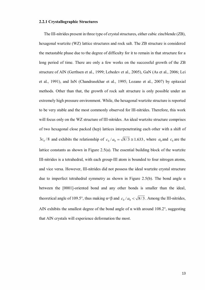
2.2 The III-Nitride Materials………………………………………………………..12
2.2.1 Crystallographic Structures……………………………………………..13
2.2.2 Defects in III-Nitride Materials…………………………………………16
2.3 Substrate Comparison for Gallium Nitride (GaN) Epitaxial Growth…………..18
2.4 Achieving Crack-free Gallium Nitride (GaN) on Silicon (111) Substrate………………………………………………………….22

ix
2.4.1 Aluminium Nitride (AlN) Nucleation Layer……………………………22
2.4.2 Nitridation Surface Treatment (NST) Technique……………………….23
2.4.3 AlN/GaN Strained-Layer Superlattice (SLS)…………………………...25
2.5 Metal Organic Chemical Vapour Deposition (MOCVD)………………………26
CHAPTER 3: RESEARCH METHODOLOGY…………………………………….33
3.1 Substrate Cleaning………………………………………………………………33
3.1.1 Organic Cleaning/ Solvent Cleaning Method…………………………..33
3.1.2 Radio Corporation of America Standard Cleaning (RCASC) Method…………………………………………….34
3.1.3 Hydrofluoric (HF) Acid Dipping Method………………………………34
3.2 Metal Organic Chemical Vapour Deposition (MOCVD)………………………36
3.2.1 Hydrogen Thermal Cleaning……………………………………………36
3.2.2 Controlled Preliminary Sample…………………………………………37
3.2.3 Aluminium Nitride (AlN) Nucleation Layer Homogeneity Test………………………………………………………38
3.2.4 Influence of Nitridation Surface Treatment (NST) Growth Time Against the Quality of the Gallium Nitride (GaN) Layer…………………………………………...39
3.2.5 Effect of Varying the Aluminium Nitride/Gallium Nitride (AlN/GaN) Strained-layer Superlattice (SLS)………………………….40
3.3 Sample Characterizations……………………………………………………….43
CHAPTER 4: RESULT AND DISCUSSION………………………………………..44
4.1 Introduction……………………………………………………………………..44
4.2 Controlled Preliminary Growth of GaN on Si (111) Substrates……………......45
4.2.1 Morphological Properties……………………………………………….46
4.2.2 Structural Properties…………………………………………………….49
4.3 Homogeneity Test for AlN Nucleation Layer…………………………………..52

x
4.3.1 Importance of Homogeneity Test……………………………………….52
4.3.2 AlN Nucleation Layer Homogeneity Test……………………………....52
4.3.2.1 Morphological Properties……………………………………….53
4.4 Nitridation Surface Treatment (NST)…………………………………………...58
4.4.1 Nitridation Surface Treatment (NST) for GaN Epitaxy on Silicon…………………………………………………58
4.4.1.1 Morphological Properties……………………………………….59
4.4.1.2 Structural Properties…………………………………………….64
4.5 AlN/GaN Strained-Layer Superlattice (SLS)…………………………………...68
4.5.1 AlN/GaN SLS for Crack-free GaN Surface…………………………….68
4.5.2 Effect of Varying the Aluminium Nitride/Gallium Nitride (AlN/GaN) Strained-layer Superlattice (SLS) Pairs……………………………69
4.5.2.1 Morphological Properties……………………………………….69
4.5.2.2 Structural Properties…………………………………………….77
CHAPTER 5: CONCLUSION AND FUTURE WORKS…………………………...81
5.1 Introduction……………………………………………………………………..81
5.2 Conclusion………………………………………………………………………81
5.3 Suggested Potential Future Works……………………………………………...83
REFERENCES………………………………………………………………………...84
LIST OF PUBLICATION AND PAPER PRESENTED……………………………96

xi
LIST OF FIGURES
Figure 2.1 : Schematic diagram of PECVD system…………………………………...6
Figure 2.2 : Schematic diagram of ALD system………………………………………7
Figure 2.3 : Slip systems in a hexagonal lattice with slip planes denoted in grey plane and slip directions indicated by black arrows…………….11
Figure 2.4 : Band gap energy vs. lattice constant for binary group III-nitride materials system………………………………………………………....12
Figure 2.5 : (a) Wurtzite crystalline structure. (b) A tetrahedral with the characteristics angles, α and β. In an ideal tetrahedral, α = β = 109.5°…………………………………………………………...14
Figure 2.6 : Illustration of wurtzite structure of AlN………………………………...15
Figure 2.7 : Schematic view for the Burgers vectors of the three types of dislocation observed in (0001) group-III nitride layers…………………17
Figure 2.8 : Mechanism of lattice mismatch in GaN grown on (a) sapphire substrate and (b) Si (111) substrate…………………………………..…20
Figure 2.9 : Mechanism of strain happening in GaN grown on (a) sapphire substrate and (b) Si (111) substrate……………………………………..21
Figure 2.10: Conventional GaN epitaxial growth on Si, (b) Cracks on surface of GaN on Si, and (c) image of meltback etching………………………21
Figure 2.11: Process gases enter the horizontal flow reactor through the three-layered gas injection nozzle inlet…………………………………30
Figure 2.12: Schematic illustration of MOCVD growth mechanism…………………31
Figure 3.1 : Schematic flow of silicon (111) cleaning process………………………35
Figure 3.2 : Growth structure of preliminary sample………………………………...37
Figure 3.3 : Schematic growth structure and the varied thickness parameter of the AlN nucleation layer…………………………………..38
Figure 3.4 : Schematic growth structure and varied nitridation time………………...40
Figure 3.5 : Schematic growth structure and varied number of AlN/GaN SLS pairs……………………………………………………..41
Figure 3.6 : Schematic diagram of experimental method……………………………42
Figure 4.1 : FESEM image of topmost GaN layer of preliminary sample…………...47
Figure 4.2 : 5 µm × 5 µm AFM image of preliminary sample………………………48

xii
Figure 4.3 : XRC scan of (002) (left) and (102) (right) plane of the topmost GaN layer of the preliminary sample…………………………..50
Figure 4.4 : FESEM cross section images of varied AlN thickness of (a) 50 nm, (b) 100 nm and (c) 200 nm thickness under 100k magnification, respectively……………………………………………...55
Figure 4.5 : Naked eye observation of the sample grown with 400 s nitridation time……………………………………………………59
Figure 4.6 : Graph of wafer bowing (µm) against nitridation time (s)……………….61
Figure 4.7 : The surface scanning images of GaN grown on Si(111) substrate at (a) 400 s, (b) 220 s and (c) 40 s of nitridation time and (d) the cross-sectional image of the GaN epitaxial growth on silicon (111) substrate at 400 s of nitridation time………………………………………………63
Figure 4.8 : The XRC measurement of (a) (0002) and (b) (101̅2) scan of samples deposited at different nitridation time……..65
Figure 4.9 : The screw and edge, mixed dislocation density of samples deposited at different nitridation time…………………………………...67
Figure 4.10: Bowing against total thickness of sample……………………………….73
Figure 4.11: FESEM surface of sample with different SLS pairs of (a) 20 pairs, (b) 40 pairs, (c) 60 pairs and (d) 80 pairs viewed under 10K magnification………………………………………..75
Figure 4.12: (a) Cross section image of overall structure under 100k magnification, and (b) Cross section image of multi-layer thickness under 200k magnification, respectively………………………76
Figure 4.13: (a) (0002) and (b) (101̅2) XRC scan for all samples deposited at different number of AlN/GaN SLS pairs………………………………..78
Figure 4.14: The screw and edge, mixed dislocation density of samples deposited at different number of AlN/GaN SLS pairs………………………………..79
xiii
LIST OF TABLES
Table 2.1: Theoretically (theo.) calculated and experimentally determined (expt.) structural parameters for AlN, GaN and InN……………………..16
Table 2.2: Comparison of substrate for GaN epitaxial growth……………………....19
Table 4.1: Growth parameters of each layer of initial preliminary sample………..... 46
Table 4.2: Structural and morphological properties of preliminary sample………….51
Table 4.3: 2D, 3D images and the properties of topmost GaN layer with variation of AlN NL thickness……………………………………………56
Table 4.4: 3D, 2D images, the rms roughness and the peak to valley value of the topmost GaN layer at different nitridation time of (a) 400 seconds, (b) 220 seconds and (c) 40 seconds, respectively……………………………………………………………....60
Table 4.5: Screw, edge and mixed, and total dislocation density for sample nitridated at different nitridation time…………………………………….66
Table 4.6: Average roughness and peak to valley (P-V) of grown sample………......71
Table 4.7: Screw, edge and mixed, and total dislocation density for sample deposited at different number of AlN/GaN SLS pairs……………………79

xiv
LIST OF SYMBOLS & ABBREVIATIONS
l Line direction
a0 Lattice constant in a direction
b Burgers vector
β2 Full width of half maximum in radian
2screwb Burger’s vector value of screw dislocation with respect to planar lattice
2edgeb Burger’s vector value of edge and mixed dislocation with respect to planar
lattice
c0 Lattice constant in c direction
CMOS Complementary metal oxide semiconductor
Dtotal Total dislocation density inside the sample
Dscrew Screw dislocation density inside the sample
Dedge Edge, mixed dislocation density inside the sample
FC Flow rate of carrier gas
FWHM Full width at half maximum
H2O2 Hydrogen peroxide
PT Total pressure above the metal organic
PV Vapour pressure of the metal organic
RMS Root mean square
TNSC Taiyo Nippon Sanso Corporation

1
CHAPTER 1: INTRODUCTION
This thesis involved the studies of the buffer layer on silicon (111) substrates by using
III-V nitrides material that is aluminium nitride (AlN) and gallium nitride (GaN). The
epitaxial technology involved the usage of nitridation surface treatment (NST), nucleation
layer and strained-layer superlattices (SLS) to compensate the lattice mismatch as well as
the thermal mismatch between the III-V nitrides to realize the formation of crack-free
GaN on silicon (111) substrates.
1.1 Introduction
The III-V nitrides is an interesting material to work with owing to its great potential to
be used for optoelectronic applications. Most works on gallium nitride technology uses
sapphire as substrate despite many limitations such as insulating property, inability of
large scale uniformity and extreme hardness (Molnar et al., 1997; Liu & Edgar, 2002).
Silicon (111) substrates have currently become an increasingly competent alternative
substrate due to its low cost, high thermal and electrical conductivity as well as capability
to be produced in large scale (Liu & Edgar, 2002; Marx et al., 1998). The most intriguing
properties of silicon as a potential substrate for GaN-based devices is the practicability
when integrating conventional silicon technology with GaN technology.
Nevertheless, the growth of high quality GaN epilayer on Si (111) is considered
challenging due to huge in-plane thermal expansion coefficients mismatch (54 %), large
lattice mismatch (16 %) and distinct crystallic structures (cubic Si against hexagonal
GaN) which promotes defect in growth of GaN epilayer (Ozturk et al., 2013). Direct
growth of GaN on Si (111) surface is challenging due to poor nucleation properties of
GaN on Si, leading to island-like GaN structures (Uen et al., 2005). Besides that, it has
been reported that at high temperature (1200 K), Si outgases and reacts with Ga causing

2
meltback etching (Pal & Jacob, 2004). This phenomenon promotes production of
polycrystalline GaN which inhibit high quality growth of GaN.
On the other hand, cracking issue arises as major problem in the epitaxy growth of
GaN/Si(111), resulting in low performance of devices due to current-scattering center for
light propagations (Krost & Dadgar, 2002). Despite the problems there has been
breakthroughs in growing GaN on silicon, e.g., Reiher et al. (2009) managed to fabricate
InGaN/GaN LED structure grown on (110)-oriented silicon substrate. Through electrical
excitation, the structure have emit light with a peak at 490 nm. However, several other
works of GaN directly on Si suffers from very low quality of GaN layer and cracks that
reduce the effectiveness of optoelectronic application especially for light emitting diode
(LED), laser diode (LD) and high electron mobility transistor (HEMT) (Tran et al., 1999;
Watanabe et al., 1993).
Outstanding improvement have been achieved in this past few years with several
interesting approach. One of them is the application of Ga-free buffer layer technique to
eliminate meltback etching issues. AlN were known as the most promising candidate for
this approach due to smaller lattice mismatch and thermal expansion coefficient between
AlN and Si as compared to GaN (Zang et al., 2004). Zamir et al. (2000) studied the
correlation of AlN buffer growth temperature towards the morphological surface and
preferred orientation of GaN. It is observed that the crystalline quality of GaN film was
improved with increasing the AlN buffer growth temperature from 700 to 760 °C.
Recently, a few groups managed to achieve good quality GaN hetero-epitaxial growth on
Si(111) substrate grown by horizontal-reactor metal organic chemical vapour deposition
(MOCVD). The above result were realized by addition of several layer above the
nucleation layer using intermediate stacking layer of AlN/GaN (Hofstetter et al., 2006)
or AlxGa1-xN/GaN (Nikishin et al., 1999), low temperature AlN interlayer (Blassing et
al., 2002) and SixN1-x interlayer (Hikosaka et al., 2014). Cracking issues were reduced

3
using AlN/GaN stacking layer in GaN heteroepitaxial growth which concluded the high
effectiveness of the layer for strain control (Egawa et al., 2005) and for dislocation
filtering (Su et al., 2015). Ubukata et al. (2007) also reported a successful crack-free GaN
on 150mm diameter Si(111) with addition of 24 nm thickness/period of AlN/GaN
(AlN:4nm; GaN:20nm) multilayer using horizontal flow MOCVD.
While other works focused on low growth temperature of AlN of within 650-750°C as
their basis towards achieving crack-free GaN on Si (111) (Zamir et al., 2000; Bläsing et
al., 2002), this work clearly highlight the ability of SR-2000 MOCVD towards achieving
high quality AlN buffer layer at higher temperature growth of 1000 °C. Strained-layer
superlattice (SLS) structure and nitridation surface treatment (NST) are introduced as
features towards achieving high quality, crack-free GaN on Si(111) substrate.
Si(111) was chosen as the substrate for this research instead of other silicon plane due
to the fact that the Si(111) plane possess two inverse three-fold symmetry that resembles
the six-fold symmetry of the hexagonal GaN (0001) plane. Thus, the six main
crystallographic directions of Si(111) plane can perfectly aligned to the six major
crystallographic directions of the GaN in (0001) plane to form an epitaxial relationship
(Liaw et al., 2000).
Towards achieving a crack free GaN layer on silicon (111) substrates by using metal
organic chemical vapour deposition (MOCVD) technique, aluminium nitride (AlN) have
been introduced as the potential material towards achieving that aim. The reason behind
of this approach is to provide a better initial point for epitaxial growth of GaN on silicon
(111) substrates. The ability of AlN to minimize cracking and compensate dislocation
will be emphasized in this thesis. Besides, device quality such as LEDs performance rely
mainly on the ability of buffer epitaxial to eliminate as much dislocation as possible
before the LED device layer were implemented onto it. Dislocations serve as non-
radiative recombination centers inside LED which reduce the internal quantum efficiency
4
of the photon to regenerates light. Thus, it is imperative to minimize the dislocation
density within the buffer layer as it will become the key for manufacturing good quality
LEDs.
1.2 Research Objectives
There are three objectives of this research towards producing a crack-free GaN layer
on Si(111) substrates. The first objective of this work is to determine the homogeneity of
the surface of AlN/GaN grown using MOCVD. Secondly, is to investigate the effect of
varying the nitridation surface treatment (NST) time with the quality of topmost GaN
layer. The third objective is mainly to investigate the effect of varying the number of
period of AlN/GaN strained-layer superlattice (SLS) to the topmost GaN layer towards
establishing a crack-free GaN layer on silicon (111) substrates.
Chapter 2 discusses the basics of crystal structure and the differences between silicon,
GaN and AlN lattices. The theory of the crystal structures will be briefly explained. The
roles of NST in the structure and the function of AlN as a potential material to filter
dislocation will also be elucidated. The mechanism of MOCVD, previous works on the
layer used and the modification that have been made from other researches will also be
discussed in detail. Chapter 3 will described the details and the parameters of the
experimental work which involved the process of cleaning the substrates, epitaxial growth
and the characterizations method used to obtain the result for this thesis. Results and
discussion of the overall work will be presented in Chapter 4. The structural and
morphological properties of the topmost GaN layer due to the insertion of AlN and other
intermediate layer will be discussed. The conclusions of this research are presented in
Chapter 5.

5
CHAPTER 2: THEORY AND LITERATURE REVIEW
The following chapter gives a brief introduction to the physics behind this work. The
necessity of introducing AlN as the nucleation layer on silicon substrate prior for the
growth of a good quality GaN epilayer will be explained by understanding the crystal
properties of materials as well as the difference in their crystal structures. It is also crucial
to understand the behaviour of solid in high temperatures and how they response towards
any temperature changes.
2.1 Introduction
2.1.1 Chemical Vapour Deposition (CVD) Techniques
The increase in demand of modern industries for increased yield and constant
enhancement of material properties to be used in electronic, optoelectronic, optical and
mechanical applications have prompted the development of various innovative film
deposition techniques. While certain deposition techniques offers unique advantages as
compared to others, each process technology has certain limitations (Wiest et al., 2006).
There are three main chemical vapour deposition (CVD) techniques that is chemical
vapour deposition (CVD), atomic layer deposition (ALD) and metal organic chemical
vapour deposition (MOCVD).
The basic mechanism of CVD process involves the chemical reactions and/or
dissociation of gaseous reactants in an activated environment (e.g. heat, plasma, light etc.)
to produce high performance and high purity thin films. The conventional CVD that most
commonly applied is the thermally activated CVD. This process can be categorized
according to the range of pressure in which the deposition takes place. These include
atmospheric pressure CVD (APCVD), low pressure CVD (LPCVD) or ultra-high vacuum
(UHCVD) depending on the processing pressure. (Wu et al., 1996; Matocha et al., 2005;
Kim et al., 2001). The other unique variants of CVD that have been used to deposit thin
6
films include metal organic chemical vapour deposition (MOCVD) [Shan et al., 1995;
Fujieda et al., 1987; Manasreh, 1996; Haffouz et al., 2003; Sakai et al., 1996), plasma
enhanced chemical vapour deposition (PECVD) (Humphreys et al., 1989), and atomic
layer deposition (ALD) (Gates & Neumayer, 2001).
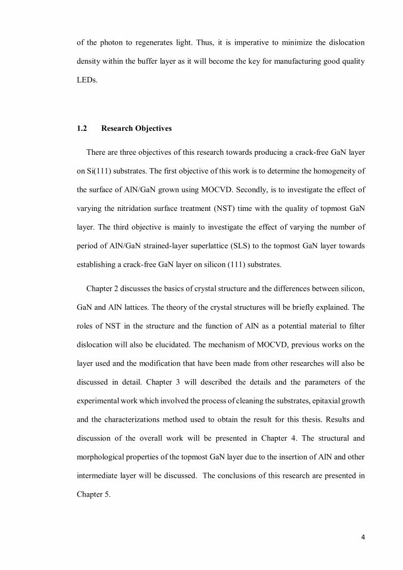
2.1.1.1 Plasma Enhanced Chemical Vapour Deposition (PECVD)
Plasma assisted or plasma enhanced CVD (PECVD) is a technique whereby electrical
energy rather than the thermal energy is used to trigger the homogeneous reactions to
produce chemically active ions and radicals. The ions and radicals then participate in
heterogeneous reactions, leading towards the formation of thin film on the substrate
(Jones & Hitchman, 2008). The main advantage of using PECVD is the ability of thin
film to be grown under low deposition temperature which is often critical in the
manufacture of semiconductors. Figure 2.1 shows the schematic diagram of the PECVD
system (Cho & Boo, 2012).
Figure 2.1: Schematic diagram of PECVD system (Cho & Boo, 2012).
7
2.1.1.2 Atomic layer deposition (ALD)
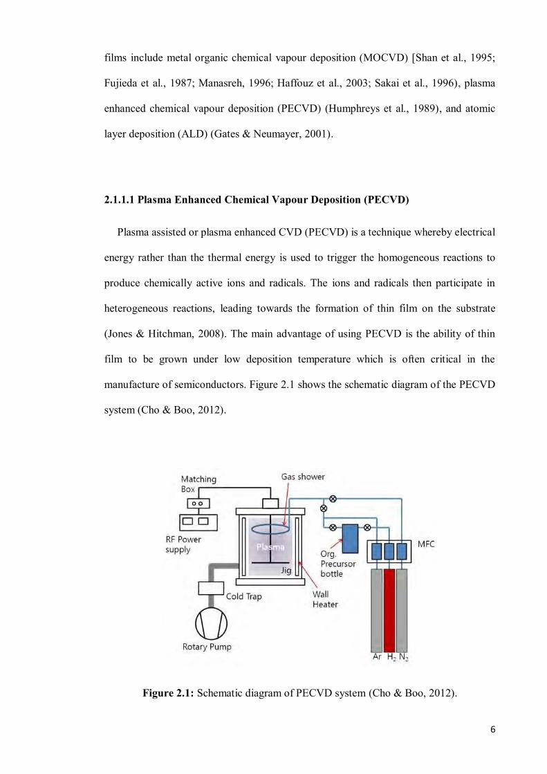
Atomic layer deposition (ALD) technique has emerged as a crucial technique in
deposition of thin films owing to its advantage to precisely tune the thickness of the films
down to angstrom or monolayer level (Pinna et al., 2012). ALD applies unique
mechanism of growth, in which monoatomic layers are deposited in sequence for a
controlled-film deposition at the sub-nanometre level. Throughout the deposition process,
the precursors are pulsed alternatively onto the substrate surface and subsequent
chemisorption or surface reactions occurs. Due to this self-limited growth mechanism,
the deposited films thickness can be precisely tailored with conformal deposition on high
aspect ratio structures and excellent step coverage (Maula et al., 2011). The distinctive
advantage of ALD has made it an attractive technique to be industrially applied for the
deposition of very thin high-k oxides in complementary metal oxide semiconductor
(CMOS) technology which serve as gate dielectrics in metal oxide semiconductor field-
effect transistor (MOSFET) devices (Ye et al., 2003) and as dielectrics in the trench
capacitor structures (Seidl et al., 2002). Figure 2.2 displays the schematic diagram of ALD
system (Dhakal et al., 2016).
Figure 2.2: Schematic diagram of ALD system (Dhakal et al., 2016).
8
2.1.1.3 Metal Organic Chemical Vapour Deposition (MOCVD)
Metal organic chemical vapour deposition (MOCVD) utilizing metal organic
compounds as precursors which is in contrary to conventional chemical vapour deposition
technique that uses inorganic precursors, containing metal halides. MOCVD offers
unique flexibility to tailor a wide range of operating conditions such as source materials,
temperature and pressure to produce state of the art performance devices such as lasers,
light emitting diodes (LEDs), laser diodes (LDs) and high electron mobility transistors
(HEMTs) using this technique. The metalorganic source basically originate from
group-III nitride films which involves high growth temperatures interacting in complex
gas phase and surface reactions. The growth mechanism and the systematic surface
reactions involved during growth will be explained in detailed in Chapter 2.
MOCVD is performed at much higher pressure than other CVD, allowing the group-
III nitride films to be grown at significantly higher temperatures (more than 1100 °C)
whereby the compound is thermodynamically stable. This favourable thermochemical
condition is believed to be the main reason why MOCVD III-nitride material performs
better for commercial optoelectronic device applications.
In this study, nitridation surface treatment process followed by a thin HT-AlN
nucleation layer was grown on Si (111) substrate. Prior to 1µm growth of GaN layer,
AlN/GaN multi-layer was grown beneath it, which act as the strain compensating and
dislocation filtering layer. The multilayer was grown by varying the number of AlN/GaN
multilayer periods of 20, 40, 60 and 80 pairs, respectively with the effort to optimize the
quality of GaN epilayer grown on Si(111) substrate. This thesis reports on the crack-free
GaN achieved in the sample by which the sample bowing, surface roughness and
dislocation density are critically affected.

9
2.1.2 Crystal Structures of Material
An atomic structure which exhibit periodicity in all directions is considered as
crystalline material, which consist of small building blocks called unit cells. A unit cell
is the smallest periodic feature in a crystal lattice. It is defined by the unit vectors of a1,
a2, a3. Any point of the lattice can be referred from another lattice point by using these
lattice vectors. The reference lattice vectors are called the Bravais lattice of the structure,
while the vector a1 is usually interpret by the shortest period in the lattice. For cubic cells,
a2 is perpendicular to a1, and a3 is perpendicular to the plane connected by a1 and a2. For
the lattice constant of cubic cell, |a1| = |a2| = |a3| = a, whereby a is the lattice constant of
the crystalline material (Morkoc, 2013).
The symbolization for a crystal plane is (h k l) and if the crystal planes are identically
symmetry, notation {h k l} can be used. A crystal plane is determined as points in which
the plane intersects the axis of the crystal lattice. The reciprocal is taken from those
coordinates and they are reduced to the smallest integers. The results denoted as Miller
indices of the crystal plane. It is crucial to mention that when specifying planes and
directions of the hexagonal wurtzite III-nitrides as well as the various crystal surfaces,
four-index Miller notation (h k i l) is usually employed where khi . Here, the overline
is used to express a negative quantity. There are three standard notations distinctively
used as follows:
(h k i l) denotes one specific plane or surface;
[h k i l] denotes one specific direction;
{h k i l} denotes equivalent planes or surfaces due to symmetry of the lattice.

10
The material is considered as a single crystal if it is consisted of a continuous lattice
which formed by an identical unit cell. While, the material is considered to be
polycrystalline, if it consists of mixed oriented grains of crystals (e.g., most metals). Other
than that, the material is called amorphous if there is no long range periodicity existed.
2.1.3 Defects in Material
The properties of semiconductor materials are often tuned by two main factors which
are the defect as well as the incorporation of impurities. The hetero-epitaxial layers
contain large densities of native and structural defects. Among the structural defects,
inversion domains, threading dislocations (TDs), pyramidical planar defects and nano-
pipes defects are the common defects that can cross the epitaxial layer.
It has been identified that defects can be classified as point defects, line defects, planar
defects and volumetric defects. Some example of point defects are vacancies (missing
atoms), interstitial atoms (additional atoms incorporated on different sites other than
substitutional sites) and anti-sites (a cation sitting on a nominal anion site, or vice versa)
atoms. A series of point defects create an imaginary line dislocations denoted as line
defects. In an ideal polycrystalline material, the grains should be perfect crystals.
However, in epitaxial growth, the grain boundaries and stacking faults (SFs) usually occur
and are considered as planar defects. A line defect can also evolve into planar defect when
there is array of line dislocations in a certain planar form. Whereas, volume defects are
usually noted as regions and voids of amorphous material inside the grown crystal
(Jasinski et al., 2003; Romano & Myers, 1997).
Dislocations are described by their line direction (l) which defines as the orientation
of the dislocation in the crystal. While, Burgers vector (b) is drawn through the dislocation
to illustrate the displacements inside the crystal structure. The Burgers vector originates

11
from the Burgers circuit, which is a loop in increments of jumps from one atom to the
next that surrounds the dislocation line. When this circuit is compared to a perfect lattice,
the loop opens and the additional component of the loop is the Burgers vector b.
Moreover, dislocations do not just end in a crystal; they either form a complete loop or
end at a crystal surface.
The three possible types of dislocations are edge, screw and mixed-type. If l is
perpendicular to b, the dislocation is an edge-type dislocation and if l is parallel to b, the
dislocation is screw-type. Mixed-type dislocations are a combination of edge and screw
types with b points neither perpendicular nor parallel to l. If the Burgers vector of the
dislocation is a lattice vector, then the dislocation is considered a perfect dislocation.
Partial dislocations happen when Burgers vectors is not equivalent to a lattice vector and
are commonly referred to the decomposition of perfect dislocations also known as a
stacking fault (Rockett, 2007). All dislocations discussed hereafter are perfect
dislocations. Figure 2.3 illustrates screw and edge dislocations in a crystal. The arrow
refers to Burgers vector with grey planes denoting the dislocation planes of each type of
dislocation.
Figure 2.3: Slip systems in a hexagonal lattice with slip planes denoted in grey plane and slip directions indicated by black arrows (Jones & Batyrev, 2012).

12
2.2 The III-Nitride Materials
The group III-elements from the periodic table like aluminium (Al), gallium (Ga) and
indium (In), when mixes with nitrogen (N) from the group V element will form a III-V
compound semiconductor material system consisting of aluminium nitride (AlN), gallium
nitride (GaN), indium nitride (InN), as well as their ternary and quaternary alloys. The
main advantages of using III-nitride materials in semiconductor applications is mainly
due to its wide coverage of bandgap energy ranges from 0.7 eV for InN to 6.1 eV for AlN
as shown in Figure 2.2. Due to such wide bandgaps, group III-nitrides rapidly emerges as
competence material in the development of various applications ranging from infrared to
ultraviolet light emitters and high temperature with high frequency transistors.
Figure 2.4: Band gap energy vs. lattice constant for binary group III-nitride materials system (Schubert, Gessmann & Kim, 2005).
13
2.2.1 Crystallographic Structures
The III-nitrides present in three type of crystal structures, either cubic zincblende (ZB),
hexagonal wurtzite (WZ) lattice structures and rock salt. The ZB structure is considered
the metastable phase due to the degree of difficulty for it to remain in that structure for a
long period of time. There are only a few works on the successful growth of the ZB
structure of AlN (Gerthsen et al., 1999; Lebedev et al., 2005), GaN (As et al., 2006; Lei
et al., 1991), and InN (Chandrasekhar et al., 1995; Lozano et al., 2007) by epitaxial
methods. Other than that, the growth of rock salt structure is only possible under an
extremely high pressure environment. While, the hexagonal wurtzite structure is reported
to be very stable and the most commonly observed for III-nitrides. Therefore, this work
will focus only on the WZ structure of III-nitrides. An ideal wurtzite structure comprises
of two hexagonal close packed (hcp) lattices interpenetrating each other with a shift of
8/3 0c and exhibits the relationship of 633.13/8/ 00 ac , where 0a and 0c are the
lattice constants as shown in Figure 2.5(a). The essential building block of the wurtzite
III-nitrides is a tetrahedral, with each group-III atom is bounded to four nitrogen atoms,
and vice versa. However, III-nitrides did not possess the ideal wurtzite crystal structure
due to imperfect tetrahedral symmetry as shown in Figure 2.5(b). The bond angle α
between the [0001]-oriented bond and any other bonds is smaller than the ideal,
theoretical angle of 109.5°, thus making α<β and 3/8/ 00 ac . Among the III-nitrides,
AlN exhibits the smallest degree of the bond angle of α with around 108.2°, suggesting
that AlN crystals will experience deformation the most.
14
Figure 2.5: (a) Wurtzite crystalline structure and (b) A tetrahedral with the characteristics angles, α and β. In an ideal tetrahedral, α = β = 109.5° (Thapa, 2010).
The space grouping for the WZ structure is P63mc in the Hermann-Maugin notation
(Morkoc, 2013). The group III-nitrides have partially ionic and partially covalent bonds.
Due to the 1s22s22p3 electronic configuration of the N atom (the most electronegative and
the smallest group-V element) and the lack of electrons occupying the outermost orbitals,
the electrons in the metal nitrogen covalent bond are dominantly attracted by the Coulomb
potential of the N atomic nucleus. This means that the covalent bond possesses stronger
ionicity due to the large difference in the electro-negativities compared to other III-V
covalent bonds, causing the III-nitrides to have high bonding energies (AlN = 11.5, GaN
= 8.9, and InN = 7.7 ev/atm) (Shul & Pearton, 2011).
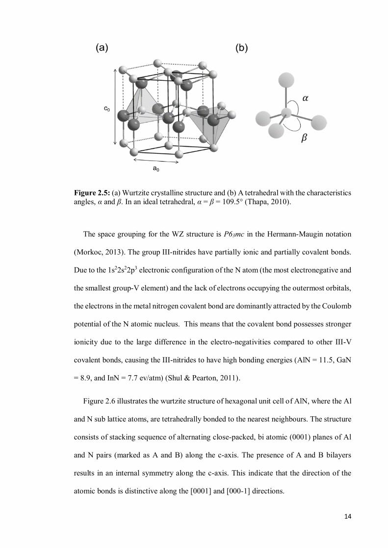
Figure 2.6 illustrates the wurtzite structure of hexagonal unit cell of AlN, where the Al
and N sub lattice atoms, are tetrahedrally bonded to the nearest neighbours. The structure
consists of stacking sequence of alternating close-packed, bi atomic (0001) planes of Al
and N pairs (marked as A and B) along the c-axis. The presence of A and B bilayers
results in an internal symmetry along the c-axis. This indicate that the direction of the
atomic bonds is distinctive along the [0001] and [000-1] directions.

15
Internal polarity of the film exists due to this difference, and is described by the
direction of the group-III-N bond arrangement between the two layers (along the c-axis)
with respect to the normal surface of the film. If the nitrogen atoms are placed on top of
the group-III atoms the film is called [0001]-polar face or Al-faced, while if the group-III
atoms are on top of the N atoms the film is called N-faced or [000-1]-polar face. The
polarity of the films crucially effect both the morphological properties and the
piezoelectric field of the group III-nitrides. The effect of polarity has been widely studied
both theoretically and experimentally in [Neugebauer, 2001; Stutzmann et al., 2001).
Group III-nitrides grown on (0001) sapphire by metal organic vapour phase epitaxy
(MOVPE) are typically group III-polar (Stutzmann et al., 2001). The other binaries InN,
GaN, their ternaries and quaternaries have identical crystalline structure, in which group-
III atoms occupy the sub-lattice shown in Al atoms position as in Figure 2.4.
Figure 2.6: Illustration of wurtzite structure of AlN (Thapa, 2010).
Technically, an unstrained AlN structure have lattice parameters of a = 3.110 Å and
c = 4.982 Å, respectively (Ambacher et al., 2002). On the other hand, GaN have lattice
parameters of a = 3.199 Å and c = 5.185 Å, respectively. Table 2.1 summarizes the
theoretically (theo.) calculated and experimentally determination (expt.) of structural

16
parameters for AlN, GaN, and InN (Stutzmann et al., 2001; Ambacher et al., 2002) where
a is the lattice constant in a direction, c is the lattice constant in c direction and u is the
length between two nearest-neighbour anion-cation bond. Unlike GaN, the
experimentally determined c/a of AlN differs significantly from the aforementioned ideal
theoretical calculation parameters: c/a = 1.601 and u = 0.379 due to the strong existence
of ionic bonds (Li et al., 2003). This may be the reason for the difficulties in doping of
AlN. Whereas, GaN and InN have smaller iconicity than AlN (Li et al., 2003) making
them easier material to be applied as n-type and p-type doped.
Table 2.1: Theoretically (theo.) calculated and experimentally determined (expt.) structural parameters for AlN, GaN and InN (Stutzmann et al., 2001; Ambacher et al., 2002). Parameters AlN GaN InN a (theo.) (Å) 3.110 3.199 3.585 c/a (theo.) 1.633 1.633 1.633 u (theo.) 0.375 0.375 0.375 u (expt.) 0.382 0.377 0.379 a (expt.) (Å) 3.112 3.1896 3.548 c (expt.) (Å) 4.982 5.185 5.705 c/a (expt.) (Å) 1.60 1.626 1.608
2.2.2 Defects in III-Nitride Materials
In the case of III-nitride epilayers, the dislocations mainly originate from lattice
mismatch during hetero-epitaxial growth or pre-existing dislocations from growth of the
single crystal native substrate. There are three possible types of dislocations observed in
III-nitrides that are: c-type with b = <0001>, a-type with b = 1/3 <11-20>, and (a + c)-
type with b = 1/3 <11-23>. The nomenclature of these dislocations referred directly to the
directions and lattice constants in the wurtzite structure as illustrated in Figure 2.7.

17
Figure 2.7: Schematic view for Burgers vectors of the three types of dislocation observed in (0001) group-III nitride layers (Thapa, 2010).
These dislocations can be edge, screw, or mixed-type depending on their dislocation
line. Dislocations that follow the growth direction are called threading dislocations (TDs)
and have a line direction parallel to the growth direction. For example, TDs in III-nitrides
grows in the c-direction have l = [0001] with c-type, a-type, and (a + c)-type dislocations
being screw, edge, and mixed-type dislocations, respectively. There is another kind of
dislocations that lie in a hetero-epitaxial interface and relieve misfit strain that is called
misfit dislocations (MDs). For the case of III-nitride growth, MDs have l perpendicular
to [0001]. MDs happened due to the difference in lattice and thermal expansion
coefficient, and TDs due to the twist and tilt of crystal grains. Below specific certain
epilayer thickness, known as the critical thickness, an epilayer could grow
pseudomorphically on the substrate, while growth exceeding the critical thicknesses will
suffer a relaxation of misfit strain via plastic flow.
During crystal growth, the unevenness of the substrate surface or the nucleation of
growth islands leads to the formation of dislocations with line direction parallel to the
growth direction. These dislocations penetrate the epilayer, which in turn coined as TDs
and reach the growth surface except those that combined and annihilate each other. The
presence of TDs significantly affects the device performances causing non-radiative

18
recombination (Rosner et al., 1997; Sugahara et al., 1998), carrier scattering effects
(Weimann et al., 1998), and diffusion of dopants and impurities (Lebedev et al., 2005).
2.3 Substrate Comparison for Gallium Nitride (GaN) Epitaxial Growth
Nowadays, sapphire substrate has established as a conventional substrate for gallium
nitride (GaN) epitaxial growth due to its considerably good properties and variable
applications. However, sapphire substrate has a few limitations and disadvantages, such
as its insulative properties, the incompatibility integration of device fabrication with
vertical-type electrode structure, relatively low thermal conductivity to dissipate heat in
high-power devices, and the limited dimension of diameter size, which make this wafer
not suitable for commercial mass production of GaN.
On the other hand, hetero-epitaxy of GaN on alpha, α 6H- silicon carbide (SiC) also
has been tremendously been investigated by several groups (Johnson et al., 1996; Torvik
et al., 1998), with successful fabrication of electronic and optoelectronic devices, such as
high electron mobility transistor (HEMT) (Kordoš et al., 2005), light emitting diode
(LED) (Madhu et al., 2005), and laser diode (LD) (Domen, 1998; Edmond et al., 2004).
However, due to limited availability, small diameter size restriction and the relatively far
more expensive price than sapphire and silicon substrate, α 6H-SiC works have been
declined in terms of publications over these recent years.
The homo-epitaxy of GaN on free-standing GaN substrate has produced a remarkable
dislocation density as low as 106 cm-2 (Hashimoto, 2006). Despite the superior epitaxial
quality that this substrate can offer, such substrate has maximum diameter size of only 2
inches and very limited availability, which leads to its extremely expensive price.
Therefore, it is only employed in high-performance devices, for which the corresponding
low dislocation density is crucial such as blue-violet LD.
19
Although the epitaxial growth of III-nitrides on sapphire, α 6H-SiC and GaN free-
standing substrate has considerably matured, there are increasing concern for the other
breakthrough for GaN-based epitaxy on silicon (Si) substrate. Si have many remarkable
properties, for instance, excellent availability, large diameter size of up to 12 inches and
extremely low cost. The best advantage in successful growth of GaN-based devices with
well-established Si-based electronic device like integrated circuits, photo-detector, and
other optoelectronic devices, is basically due to the ability of allowing the fabrication of
multi-function hybrid device on a single wafer.
In the comparison with conventional sapphire substrate, Si have tuneable electrical
conductivity by undergoing a process known as doping and has better thermal
conductivity, which greatly improves the thermal dissipation in particularly for high
power with high temperature device operation. Si also are conductive in nature which
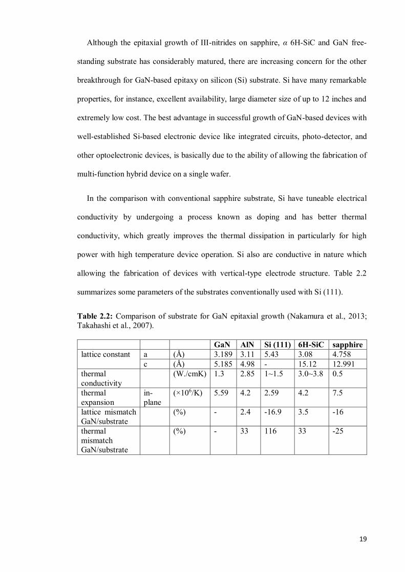
allowing the fabrication of devices with vertical-type electrode structure. Table 2.2
summarizes some parameters of the substrates conventionally used with Si (111).
Table 2.2: Comparison of substrate for GaN epitaxial growth (Nakamura et al., 2013; Takahashi et al., 2007). GaN AlN Si (111) 6H-SiC sapphire lattice constant a (Å) 3.189 3.11 5.43 3.08 4.758
c (Å) 5.185 4.98 - 15.12 12.991 thermal conductivity
(W./cmK) 1.3 2.85 1~1.5 3.0~3.8 0.5
thermal expansion
in-plane
(×106/K) 5.59 4.2 2.59 4.2 7.5
lattice mismatch GaN/substrate
(%) - 2.4 -16.9 3.5 -16
thermal mismatch GaN/substrate
(%) - 33 116 33 -25

20
Nonetheless, GaN epitaxy on Si substrate is more challenging than on sapphire or α
6H-SiC substrates. Perhaps the main drawback of epitaxy of GaN on Si was due to large
thermal coefficient mismatch of 116 % between the GaN and Si which lead towards the
formation of cracks during the cooling phase after growth process since the lattice
constant mismatch for GaN/Si(111) of -17 % is almost similar to GaN/sapphire of 16 %
as shown in Figure 2.8. Simultaneously, the mechanism of strain also happening as shown
in Figure 2.9. The GaN-Si reaction during growth also forms amorphous meltback-
etching layer when conventional growth technology in Figure 2.10(a) is applied.
However, the above growth challenges can be overcome by controlling the epitaxial
growth using buffer layer techniques to obtain high quality GaN epitaxy on Si substrate.
Figure 2.8: Mechanism of lattice mismatch in GaN grown on (a) sapphire substrate and (b) Si (111) substrate (Zhu, 2012).
(a) (b)

21
Figure 2.9: Mechanism of strain happening in GaN grown on (a) sapphire substrate and (b) Si (111) substrate (Zhu, 2012).
Figure 2.10: (a) Conventional GaN epitaxial growth on Si, (b) Cracks on surface of GaN on Si, and (c) image of meltback etching (Zhu, 2012).
(a) (b)

22
2.4 Achieving Crack-Free Gallium Nitride (GaN) on Silicon (111) Substrate
This research focuses on the effect of nitridation surface treatment prior to the growth
of high temperature (HT) AlN nucleation layer and followed by the AlN/GaN super-
lattice structure (SLS) which then end with a thick GaN epilayer atop.
2.4.1 Aluminium Nitride (AlN) Nucleation Layer
It has been understandable that silicon (Si) substrates offer several challenges in
growing a non-cracking homogeneous gallium nitride (GaN) epilayer on top of it. In line
with this, several research groups have initiated a remarkable works in order to encounter
this issue (Ableet al., 2005; Dadgar et al., 2002; Arslan et al., 2008). Epitaxial engineering
knowledge have been extensively used to optimize the growth condition of epitaxial
layer. The most established technique to prevent the non-cracking issue is by introducing
the AlN nucleation layer on top of Si substrate.
The wurtzite structure of AlN provides the good basal plane for the subsequent growth
of GaN layer on top of it. The thermal expansion coefficient of AlN also compensates the
thermal expansion coefficient of GaN on Si by introducing compressive strain to the GaN
layer during the cooling phase and prevent the cracking issue (Able et al., 2005).
However, aluminium parasitic reaction during AlN growth deteriorates most of the works
during the early stage of this approach. Moreover, the insufficient mobility of AlN to
restructure on Si which causes the high tendency of AlN to produce island formation
increase the dislocation site on the structure and results in bad epitaxy of GaN (Dadgar et
al., 2002).
The above issue has initiated the needs to optimize the growth parameter for the AlN
layer. The initial effort by using low temperature (LT) AlN in range of 650-750 °C to
increase the strain compensation effect in the structure inhibit the crystal

23
restructuralization of AlN and most growth suffers high dislocation when the AlN
thickness is more than 10 nm (Kim et al., 2001). Although, a thin nucleation layer of AlN
is good for device structure, the thickness is insufficient to prevent meltback-etching in
the sample. While most works optimize the LT-AlN layer, this research will focus more
on growing high temperature AlN nucleation layer to increase the surface mobility of
AlN as well as to avoid island formation of AlN layer. This research will highlight the
ability of HT AlN layer to coalesce and reduce the dislocation density in Chapter 4.
2.4.2 Nitridation Surface Treatment (NST) Technique
In vertical configuration LED structure, the conductivity of the topmost GaN layer is
an important parameter to control. Introducing AlN into the structure will produce
adversing effect depending on the thickness of the AlN nucleation layer during growth
process. Thick AlN nucleation layer is insulative and prevents the steady flow of current
in vertical configuration devices. Thinning the AlN nucleation layer should counter this
issue but arises different problem in the epitaxy process due to insufficient thickness of
AlN to prevent meltback etching into the structure. Therefore, in this work, nitridation
surface treatment is introduced as preparatory layer to prevent silicon outgassing into the
GaN structure. The ability to grow AlN below its critical thickness will also avoids lattice
misfit in the structure due to pseudomorphic growth of layer and will reduce the
dislocation inside the structure.
Recently, significant work has been reported on the growth of a single-crystalline GaN
on Si substrate, where it has been realized by manipulating the growth temperature, buffer
layer thickness, ammonia (NH3) flow rate and the compound concentration. Uen et al.
(2005) studied the effect of in-situ substrate nitridation temperature on the overall GaN
crystalline quality where the nitridation process was conducted at 750, 950 and 1120 oC,
24
respectively. The applied temperature during nitridation process greatly contributes
towards the surface morphology as well as photoluminescence (PL) spectra of the top
GaN epilayer grown on the formed silicon nitride (SiNx) layer. Wuu et al. (1999) showed
that in order to achieve a mirror-like GaN epilayer, the pre-annealing and post-annealing
of GaN growth must be optimized thoroughly. The works illustrate the dramatic re-
evaporation of GaN layer induced at longer annealing period with a smaller grain size. It
is also reported that the NH3 flow rate significantly improve the homogeneity of the
growth GaN epilayer on Si substrate. Arslan et al. (2009) studied the effect of nitridation
time on the morphological properties of GaN grown on Si(111) substrate. Selected area
electron diffraction (SAED) results suggest that the crystal orientation of Si(111) was
found to be transferred through the amorphous SiNx layer into AlN and GaN layers. It is
concluded that it was important to prevent thick growth of SiNx layer which could cause
a polycrystalline deposition of GaN on Si(111) substrate. Meanwhile, Ozturk et al. (2013)
has published a study involving the strain analysis of GaN layer grown on nitridated
Si(111) substrate using high-resolution x-ray diffractometer; in which the nitridation time
highly influenced the strain generation in between each epitaxial layer.
The V/III ratio of each layer is calculated using the equation:
6104.22
1min)/(
min)/(
4
3
molFFFFmolF
ratioIIIV
SiHTMITMGTMA
NH
(2.1)
Since nitridation surface treatment only involve the flow of ammonia (NH3) without
any flow of group III precursor, the V/III ratio is not considered for that layer. The V/III
ratio is one of the main parameter which determines the growth direction and preferred
surface orientation of each layer. Furthermore, the crystal quality is closely related with
the change in V/III ratio of each layer. Yang et al. (2000) highlighted the influence of
V/III ratio in the low temperature aluminium nitride (LT-AlN) interlayer towards the
crystal quality of the topmost GaN layer. The author concluded that V/III ratios of the
25
LT-AlN interlayer could greatly affect the crystal quality of GaN, instead of the strain
status. Such dependence could be explained in terms of the different LT-AlN surface
morphologies originating from the tunable V/III ratios and the consequential distinct GaN
growth rates in vertical and lateral direction. The LT-AlN grown with optimizing V/III
ratio can efficiently avoid the propagation of the thread dislocations in the structure of
GaN epitaxial.
Dadgar et al. (2003) and Krost et al. (2003) also found that both the thickness and the
growth temperature of LT-AlN layer could strongly influence the strain relaxation status
and the overall quality of the GaN layer grown on LT-AlN interlayer respectively.
2.4.3 AlN/GaN Strained-layer Superlattice (SLS)
Multilayer and/or strained-layer superlattice (SLS) epitaxial technique is significant to
control crack generation in III-nitride growth. During cooling phase of MOCVD growth,
the reactor temperature ramp-down to room temperature and generates bowing effect into
the sample due to different lattice coefficient of materials of each layer. It generates
concave wafer curvature and cracks on the epitaxial layer due this difference, which leads
to difficulty in producing thick GaN epitaxial layer. SLS is also effective to reduce misfit
dislocations resulted from lattice mismatch of GaN-based epitaxial layer and the
underlying Si substrate. Threading dislocation (TDs) can be modulated to prevent them
from penetrating to the surface using SLS due to the abruptness in lattice change between
AlN and GaN below their critical thickness.
When a stack of two types material with different lattice constant is grown coherently,
lattice strain is built upon the interface of the two different materials producing a strong
strain effect on the overall SLS layer when accumulated together. Therefore, TDs which
reach the SLS interface are bent by the strain, and reaction between inclined TDs will

26
create dislocation close-loop, preventing the TDs from penetrating vertically into the
device layer. The SLS structure creates multiple built-up interface strain for TDs
inclination to happen, thus, preventing dislocation to reach the topmost GaN layer. If the
lattice strain is weak, it is not possible to bend the threading dislocations causing it to
penetrate through the structure (Gian et al., 1996). Meanwhile, SLS with too large lattice
strain will generate production of new misfit dislocation. Thus, the SLS thickness,
abruptness and repeatability of each layer should be precisely controlled so that the SLS
function effectively as dislocation filtering layer.
In vertical flow MOCVD, abrupt and uniform SLS is almost impossible to grow due
to the deposition mechanism and the flow of precursor which have high tendency to
produce air turbulence during growth of SLS (Meng et al., 2013). This research takes the
advantage of using horizontal flow MOCVD which able to produce a uniform, steady
flow of precursor throughout the deposition process to produce a very uniform and abrupt
with precise repeatable layer in which the results are shown in
Chapter 4.
2.5 Metal Organic Chemical Vapour Deposition (MOCVD)
The first MOCVD growth in the world was done by Manasevit & Simpson (1971),
two chemists working at Rockwell corporation who coined the term “metal-organic”
(MO) emphasizing the metal component and further published literatures describing the
MOCVD of III-V semiconductors including GaN and AlN, demonstrating the flexibility
of this process. Since then, MOCVD have been one of the dominant industrial processes
for the fabrication of semiconductor and optoelectronic devices as it offers the advantage
of conformal step coverage and deposition over a large scale. The basic working
mechanism of MOCVD is to carry precursor materials into a deposition chamber where

27
they are uniformly distributed over the surface of the substrate and decompose via
pyrolysis to produce a uniform epitaxial layer of material. The most commonly used
source of nitrogen for the III-nitrides growth is anhydrous ammonia, a liquid which has a
sufficiently high equilibrium vapour pressure at room temperature which then been
delivered directly to the deposition chamber as a gas.
The most commonly used MO sources are trimethylaluminium (TMA),
trimethylgallium (TMG) and trimetyhilindium (TMI). At room temperature, TMA and
TMG are liquids while TMI is solid, in order to abstain them from being delivered directly
into the chamber. The three MO were packed in sealed metal containers, known as
bubblers, due to their pyrophoric nature. In order to transport the MO materials to the
reactor, a carrier gas mainly hydrogen and/or nitrogen is flowed into the bubblers where
it goes through a plunge tube submerged in the MO. The carrier gas becomes saturated
with the vapour phase MO that is present above the liquid level after “bubbling” process.
The carrier gas then delivers this vaporized MO into the reactor.
The important factor that should be taken into account is the amount of MO that is
being delivered into the reactor. The amount of MO delivered into the reactor depends on
the equilibrium vapour pressure and typically calculated in micromoles. The flow rate of
MO material out of the bubbler in moles/minute can be calculated as:
VT
VCOM PP
Pmolcm
sccmFmolM
)/(400,22)(
min)/( 3 (2.1)
where CF indicates the flow rate of the carrier gas, TP is the total pressure above the
MO, and VP is the vapour pressure of the MO. The vapour pressure of the MO can be
modelled for a specific material at absolute temperature T using the parameters a and b
by the equation
TbaPV /)log( (2.2)

28
By referring to Equation 2.2, the exponential temperature dependence of VP needs the
bubblers to be dip in chilled water baths to avoid fluctuation in temperature which can
disturb the constant uniform delivery of MO. The ammonia can be considered as an ideal
gas with the molar flow rate calculated using the equation:
)/(400,22
)(min)/(
3
3
3 molcmsccmF
molM NHNH (2.3)
The ratio 3NHM / OMM calculated from Equations 2.3 and 2.1 is termed as the V/III ratio
and is a very useful parameter to describe the growth processes to determine the properties
of the deposited material. Hydrogen and nitrogen is the carrier gas that were used in SR-
2000 MOCVD system. It is noted that hydrogen gas is more suitable for thicker layer of
deposition while nitrogen is efficiently useful for growing thin layer of material. Nitrogen
is also preferred to be used for processes involving indium since hydrogen has an adverse
impact on indium corporation.
The hydrogen pellet and ammonia are stored in high pressure gas cylinders that are
reduced by a systematic pressure regulators flow system located in the gas yard before
they are connected to the system. On the other hand, nitrogen was kept in the form of
liquid in a big nitrogen tank which are pressurized to become gas to be used by the system.
From there, the gases and the MOs that flow through the system is electronically
controlled by using a vast system of mass flow controllers (MFCs), pneumatic valves and
pressure controllers. The MFC consists of a main gas flow cavity through which the flow
is being regulated using an electronically controlled valve. A small portion of the flowing
gas is carried into a capillary tube from the flow cavity with two thermalled temperature
sensors. The flow rate can be determined based on the temperature different of the sensors
in the capillary tube following this equation
TFCq p (2.4)

29
where q is the heat lost, F is the flow rate, pC is the heat capacity, and T is the change
in temperature. Obtaining this information, the control valve adjust electronically to
match the flow to the given set point. The dependency of the flow rate calculation towards
specific heat capacity of certain gas requires the MFC to be calibrated for a specific gas.
Due to the number of crucial elements involved, an automated system is essential in
handling the gas system. A computer is usually connected to the mainboard of the
MOCVD system, with a programmable logic controller (PLC) acting as an intermediate
interface between the computer and gas handling components such as valves and MFCs.
The PLC applies a set of safety interlocks, which are constantly checked before any
commands is executed from the computer. It provides safety features which guards the
user from mistakes or malfunctions which cause certain undesirable routing problems
such as toxic gas leaking into the environment.
The MOCVD growth chamber is where the formation of thin films take place. The
growth chamber design is very important for the MOCVD process to a degree that by
having the same identical design of chamber and flow channel then only a growth can be
identical in terms of result and quality. There are basically two common types of MOCVD
that depends on the way the gas will flows into the MOCVD chamber, the vertical and
horizontal MOCVD. In the vertical configuration, the gases are introduced from the top
inlet, and perpendicularly flow downward onto the substrate placed on the susceptor.
While in the horizontal reactor, the gases are flowed horizontally from the three-layered
gas injection nozzle inlet and stream tangentially to the growth site. The top nozzle carries
hydrogen and nitrogen gas known as gas carry to counter balance the pressure from the
other two lower inlets.
The middle inlet transport the MO sources to the growth sides by means of carrier
gases such as hydrogen and nitrogen gas. Whereas, the bottom inlet carries ammonia to

30
be used as nitride element during the deposition. Figure 2.11 illustrates the incoming gas
process entering the horizontal flow reactor through the three-layered gas injection nozzle
inlet. The main advantage of using horizontal MOCVD as compared to vertical MOCVD
is due to the capability of producing a very uniform and homogenous growth layer on the
substrate and thus increasing the yield of deposition per unit area per wafer.
Figure 2.11: Process gases enter the horizontal flow reactor through the three-layered gas injection nozzle inlet (“Side inlet design illustration”, 2017).
The fundamental necessity for the efficient control of MOCVD deposition process lies
in the ability of the MOCVD to retain the laminar flow during growth. It is a well-known
that, the turbulence gas effect that usually occurred inside the chamber can be avoided
under laminar flow condition. This property lead towards a uniform layer of thin film to
be deposited. The other factor that contributes to the uniformity of the grown thin film
layer is the rotating disk that is connected to the stage inside the reactor where the
susceptor is placed upon. It consists of a rotating disk as the susceptor which holds the
wafer and rotate at a desirable speed (normally set to 10 rpm) against a continuous stream
of gases flowing toward it at a normal angle. All the way during growth process, the disk
will rotate at a fixed rotation which providing a stable, homogenous and uniform layer of
thin film throughout the entire substrate surface. Figure 2.12 shows the schematic
illustration of MOCVD process that ensues on the substrate during growth.

31
Figure 2.12: Schematic illustration of MOCVD growth mechanism (Nagendra, 2009).
In general, the MOCVD process involves the following crucial steps:
1. Formation of active gaseous reactant species.
2. Transport of the reactant species into the reaction chamber.
a. The precursor or MO in the form of vaporized reactants is transport into
the chamber by carrier gas (reactive gases such as hydrogen or inert gas
that is nitrogen).
b. The delivery of reactants directly depends on the carrier gas flow rate,
pressure of the MO bottle and the source/bubbler temperature as indicated
in equations 2.1 and 2.2.
c. High purity (i.e. 99.9999 %) gaseous reactants or carrier gas is being used
with flow rate being precisely controlled using mass flow controllers
(MFC).
3. Gaseous reactants undergo gas phase reactions creating intermediate species.
a. The precursors react with NH3 at a high temperature leading to
homogeneous gas phase reaction, where intermediate species can be
formed which further undergo subsequent decomposition and/or chemical
reaction, producing powders and volatile by-products in the gas phase.

32
b. Below the dissociation temperature of buffered phase, diffusion of
intermediate species across the boundary layer occur. The diffusion rate
depends on the parameter of the deposition such as temperature, pressure,
concentration of the precursor and the design of the reactor.
4. Absorption of gaseous reactants onto the heated substrate surface and the
heterogeneous reaction occur. The process result in deposit and by-product
species.
5. The diffusion of the deposits along the heated substrate surface creating the
crystallization centre and the growth of the film is initiated.
6. Unreacted gaseous precursors and by-products will be evacuated away from the
deposition chamber to exhaust.

33
CHAPTER 3: RESEARCH METHODOLOGY
This chapter describes an overview of the process for nitridation surface treatment
(NST), deposition of aluminium nitride (AlN) nucleation layer and AlN/GaN
strained-layer superlattice (SLS) using the reactor described in the previous chapter. The
detailed steps and flow of the experiment are described concisely.
3.1 Substrate Cleaning
The silicon (111) wafer undergoes the substrate cleaning process before being
deposited in metal organic chemical vapour deposition (MOCVD) reactor. There are
mainly three subsequent steps in the cleaning process for silicon (111) wafer that is the
organic cleaning, the Radio Corporation of America standard cleaning (RCASC) method
and lastly the hydrofluoric acid (HF) dip cleaning (Bachman, 1999).
3.1.1 Organic Cleaning/Solvent Cleaning Method
The silicon (111) wafer were immersed in a contained beaker filled with acetone inside
the water bath at temperature of 50°C for 10 minutes. Consequently, the substrates were
rinsed in deionized (DI) water for 5 times. The acetone dip steps were repeated thoroughly
for one more time. After the second acetone dip was carried out, the silicon wafer were
submerged in propanol to remove the acetone residue on the surface of the substrates.
The contained beaker of propanol with the wafer were put in the water bath for 10 minutes
before being rinsed with DI water for another 5 times. After that, the wafer were dried
using nitrogen blowing on the surface of the silicon wafer.
34
3.1.2 Radio Corporation of America Standard Cleaning (RCASC) Method
This cleaning method was developed by Werner Kern and functioned to remove
organic residues and particles on the silicon wafer surface (Bachman, 1999). The
treatment is by introducing a thin layer of silicon dioxide (SiO2) layer on the silicon
surface with a certain degree of metallic contamination that shall be removed in the
subsequent cleaning steps. The RCASC involved the heating of 65 ml of ammonia
solution (NH4OH) to 70 +/- 5 °C using hot plate. The next step involved the mixing of 65
ml of hydrogen peroxide (H2O2) into the solution. The magnetic stirrer were used to stir
the solution well. The indicator for a good mixture of RCASC is the vigorously bubbling
effect that can be observed one minute after the stirring process takes place. The silicon
(111) wafer were then immersed in the RCASC solution for 10 minutes before being
rinsed with distilled water for 5 times. The silicon wafer were then dried using nitrogen
blowing. The RCASC solution can be reused within 24 hours at room temperature and 30
minutes at 70 °C.
3.1.3 Hydrofluoric (HF) Acid Dipping Method
Hydrofluoric acid (HF) is mainly used to remove the native silicon dioxide layer which
is formerly produced during the RCASC cleaning method. Due to the reactive nature of
HF which easily corrodes glass container, only polypropylene container and syringe were
used during the overall process. 480 ml of DI water and 20 ml of HF were stirred slowly
for 1 minute to produce the solution of HF before the silicon (111) wafer were dipped for
5 minutes. The silicon (111) wafer will then undergoes simple wetting test as an indicator
for checking the effectiveness of HF dip process. Little deionized (DI) water were poured
on the surface of the wafer to check the hydrophobicity of silicon wafer. If the water rolls
of and beads up, the surface is hydrophobic.

35
Since pure silicon is hydrophobic and oxide is hydrophilic in nature, a non-wetting
surface suggests an oxide-clean surface. The silicon wafer were then dried with nitrogen
blowing before being put into the metal organic chemical vapour deposition (MOCVD)
reactor for deposition process. The HF solution can be reused for repeated cleaning
process since it does not lose its effectiveness with time. The overall cleaning process
takes around 1 hour and 30 minutes and Figure 3.1 shows the schematic flow of silicon
(111) cleaning process.
Figure 3.1: Schematic flow of silicon (111) cleaning process.

36
3.2 Metal Organic Chemical Vapour Deposition
Metal organic chemical vapour deposition (MOCVD) that were used throughout this
experiment was from Taiyo Nippon Sanso Corporation (TNSC) model SR-2000 which
have the capability of growing up to 4 inch wafer inside the reactor. For the purpose of
preliminary serial of experiment and the suitability of budget, 2-inch silicon (111) wafers
were chosen as the substrate throughout this research. The reactor is a laminar flow
MOCVD design which inhibit turbulences in the gas flow resulting in precise control of
film thickness and material composition. The metal organic (MO) precursor compounds
employed in this experiment are trimethylgallium (TMGa), trimethylaluminum (TMAl)
and ammonia gaseous (NH3) which provides the reactant source materials for Gallium
(Ga), Aluminum (Al) and Nitrogen (N) respectively. Hydrogen (H2) and nitrogen (N2)
gas was supplied as the gas carrier to accommodate the transport of MO into the reactor
along the epitaxial growth.
3.2.1 Hydrogen Thermal Cleaning
The process was initiated immediately after the cleaning process by treating the silicon
surface by using in-situ hydrogen cleaning method inside the MOCVD reactor. The
transferring process from the nitrogen blowing site to the metal organic chemical vapour
deposition (MOCVD) reactor usually produce a thin layer of native oxide layer due to the
high reactivity of oxygen with silicon surface. Thus, in order to remove the native oxide
layer on the surface, hydrogen cleaning was carried out on the surface of the wafer by
heating the substrate to a deposition temperature of 1125 °C while flowing hydrogen into
the chamber for 10 minutes.

37
3.2.2 Controlled Preliminary Sample
In order to prepare the Si substrate for the subsequent growth process, the nitridation
surface treatment (NST) was carried out by supplying an ammonia (NH3) flow of 5 slm
at 1000 °C for 400s. After the NST process, a 20 nm aluminium nitride (AlN) nucleation
layer is grown at the same temperature followed by growing a 20 pairs of aluminium
nitride/gallium nitride (AlN/GaN) multi-layer with thickness of 11 nm and 13 nm,
respectively. Finally, a 500 nm thick of undoped gallium nitride (ud-GaN) epilayer was
grown atop. This deposition is the first preliminary experiment to determine the initial
condition of the growth. Figure 3.2 shows the growth structure of the preliminary sample.
Figure 3.2: Growth structure of preliminary sample.

38
3.2.3 Aluminium Nitride (AlN) Nucleation Layer Homogeneity Test
After obtaining the result for the preliminary experiment, with an effort to study the
homogeneity of high temperature aluminium nitride (HT-AlN) layer, the thickness of HT-
AlN were varied to three different thickness of 50, 100 and 200 nm, respectively. The
reason for carrying out the homogeneity test is to analyse the capability of SR-2000 to
produce a stable thin film of AlN nucleation layer as a preparation for the subsequent
growth of AlN/GaN strained-layer superlattice (SLS) on top of it. The second reason is
to determine the effect of surface uniformity of HT-AlN at different thickness towards
the topmost GaN layer. The resulting effect was then observed on the top gallium nitride
(GaN) layer while maintaining the parameters of the other layer. Figure 3.3 shows the
schematic growth structure and the varied parameter of the AlN nucleation layer.
Figure 3.3: Schematic growth structure and the varied thickness parameter of the AlN nucleation layer.
39
3.2.4 Influence of Nitridation Surface Treatment (NST) Growth Time Against the
Quality of the Gallium Nitride (GaN) Layer
Consecutively, in order to study the influence of nitridation time towards the quality
of the growth top gallium nitride (GaN) layer, the epitaxial growth process was repeated
while varying the nitridation layer growth time to 40, 220 and 400 seconds. The
parameters for the other layers are kept constant while the aluminium nitride layer
thickness was fixed to 20 nm. The reason of using 20 nm for the aluminium nitride (AlN)
nucleation layer originates from the idea that in term of device performance, thin AlN
nucleation layer performs better when compared to thicker nucleation layer (Lahreche et
al., 2000). This is due to aluminium properties which have a wide band gap of 6.2 eV.
The wide band gap acts as a barrier for the conduction of electron from the valence to the
conduction band. A thick layer of barrier increased the threshold voltage of device and
thus, reduce the current conduction in optoelectronic devices such as light emitting diode
and laser diode. However when the thickness of the AlN is thin enough (approximately
20 – 30 nm) the electron can easily tunnels from valence to conduction bands and reduce
the threshold voltage of the devices.
On the other hand, if the AlN nucleation layer thickness is too thin
(approximately ~5 nm), the hydrogen might etch the AlN nucleation layer back creating
a rough amorphous layer of AlN. Meltback etching dominates the growth, which induces
the polycrystalline growth of gallium silicide in the sample. On top of the AlN nucleation
layer, 60 pairs of AlN/GaN SLS was deposited to prevent the threading dislocation
density from propagating up the substrate and contributes to higher dislocation density in
the sample. The reason for choosing 60 pairs of SLS is to ensure the topmost GaN is
crack-free. The effect of the nitridation surface treatment (NST) growth time was
evaluated by analyzing the topmost GaN layer. Figure 3.4 shows the schematic growth
structure and the varied parameter of the nitridation surface layer.

40
Figure 3.4: Schematic growth structure and varied nitridation time.
3.2.5 Effect of Varying the Aluminium Nitride/Gallium Nitride (AlN/GaN)
Strained-layer Superlattice (SLS)
After analysing the characterization result of the earlier series involving both the
nitridation layer and the aluminium nitride (AlN) nucleation layer, a new series of
experiment was conducted to study the effect of varying the number of period of
aluminium nitride/gallium nitride (AlN/GaN) strained-layer superlattice (SLS) pairs on
the quality of the topmost GaN layer. The number of period of AlN/GaN SLS was varied
to 4 different pair numbers of 20, 40, 60 and 80 pairs, respectively. The nitridation surface
treatment was done for about 400 seconds and the thickness of the AlN nucleation layer
was fixed to 20 nm. The effect of varying the pair numbers against the whole structure
performance was determined by evaluating the topmost GaN layer of the sample. Figure
3.5 shows the schematic growth structure and the varied parameter of the AlN/GaN SLS.

41
Figure 3.5: Schematic growth structure and varied number of AlN/GaN SLS pairs.
All the sample sets were compared with the controlled preliminary sample to
investigate the effect of variation of parameter of each layer. Figure 3.6 shows the overall
experimental flow for this research towards achieving crack-free growth of GaN on Si
(111) substrate.
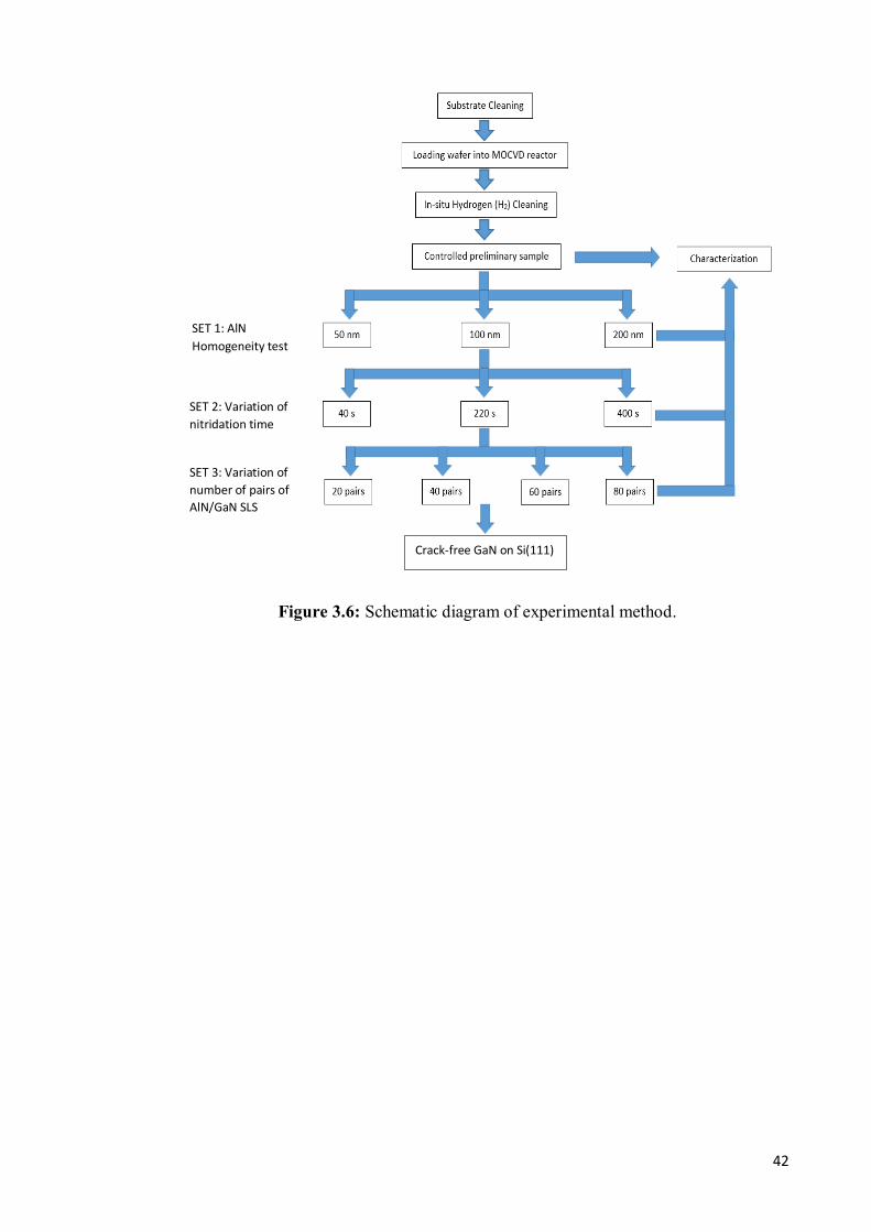
42
Figure 3.6: Schematic diagram of experimental method.
SET 1: AlN
Homogeneity test
SET 2: Variation of
nitridation time
SET 3: Variation of
number of pairs of
AlN/GaN SLS
Crack-free GaN on Si(111)
43
3.3 Sample Characterizations
The properties of the as-deposited samples were investigated using various
characterization methods. Total of 10 samples were examined using various
characterization methods to determine its properties. The surface morphological
properties of the topmost GaN epilayer grown on Si (111) substrate were analyzed by
Park System (XE-100 Model) atomic force microscopy (AFM) and Hitachi (SU8000
Model) field effect scanning electron microscopy (FESEM). Next, surface profilometer
was used to evaluate the degree of wafer bending or wafer bowing in the sample. The
wafer bowing is measured using surface profilometer across the whole wafer and was
determined to be the height difference between the center and the edge of the Si substrate.
Subsequently, the full width at half-maximum (FHWM) of both symmetric and
asymmetric ω-rocking curves were measured by x-ray rocking curve (XRC) measurement
using PANalytical XRD to determine the crystallinity of the topmost GaN layer.
Quantitatively, the screw, edge and the total dislocation density of all the samples were
calculated.
44
CHAPTER 4: RESULT AND DISCUSSION
4.1 Introduction
This chapter will show the results of the deposition throughout this research. A
preliminary sample was first deposited and characterized to provide the initial growth
results for gallium nitride (GaN) grown on silicon (Si) (111). Next, 3 sets of variation in
growth parameter consisting of three different layers in the structure were deposited and
the results were compared and analysed with respect to the first controlled growth
condition. The effect of changing the parameter is described in detail.
Two types of characterization were done on the sample involving the morphological
and the structural properties of the topmost GaN layer grown under different growth
parameter. The surface morphology of the topmost GaN layer were analysed using atomic
force microscopy (AFM) where the average surface roughness and peak to valley value
are determined. In order to confirm the morphological structure of the sample, surface
scanning was carried out using field effect scanning electron microscopy (FESEM)
measurement.
Hetero-epitaxial deposition which involves the stacking of two distinct materials with
different thermal expansion coefficient is expected will induces the bending effect on the
sample. Thus, as a step to determine the degree of wafer bending inside the sample,
profilometric scan was done across the surface of the 2 inch wafers. Next, x-ray rocking
curve (XRC) measurement was carried out using high resolution x-ray diffractometry
(XRD) analysis at both symmetric and asymmetric plane of GaN to determine the type as
well as the value of dislocation density that is generated at the topmost GaN layer. The
function and the importance of each layer in altering the dislocation density for each
growth will properly be discussed in detailed.
45
Chapter 4.2 will highlight the results and discussion of the preliminary growth
condition. While Chapter 4.3 will discuss more on the homogeneity test of aluminium
nitride (AlN) which includes the comparison of results with the preliminary sample. The
importance of producing a thin uniform layer of AlN is also discussed from device
perspective. Chapter 4.4 will analyse the effect of optimizing the nitridation time towards
the quality of the topmost GaN layer. The importance of nitridation surface treatment as
second in-situ growth preparation steps is highlighted accordingly. Chapter 4.5 will show
the result of varying the number of AlN/GaN strained-layer superlattice towards the
overall quality of the topmost GaN layer. The function of AlN/GaN SLS as dislocation
filtering will be discussed in detail. Lastly, Chapter 4.6 will highlight the main
achievement of this research in producing crack-free GaN epitaxy up to 1 micron on Si
(111) substrates. The relationships and the importance of each layer in producing a good
epitaxial deposition will be discussed in this chapter.
4.2 Controlled Preliminary Growth of GaN on Si (111) Substrates
The first preliminary growth parameter of GaN on Si (111) substrates was determined
based on several initial commissioning recipe during the installation period of metal
organic chemical vapour deposition (MOCVD) equipment at University of Malaya back
on February 2014. The growth parameter of each layer is summarized in Table 4.1.
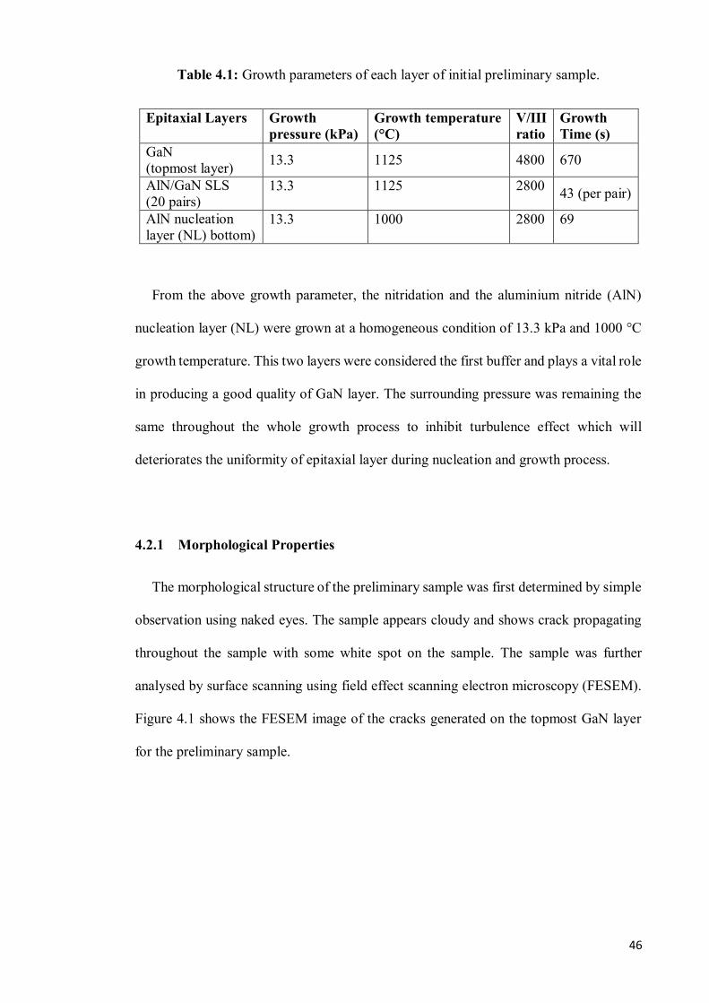
46
Table 4.1: Growth parameters of each layer of initial preliminary sample.
Epitaxial Layers Growth pressure (kPa)
Growth temperature (°C)
V/III ratio
Growth Time (s)
GaN (topmost layer) 13.3 1125 4800 670
AlN/GaN SLS (20 pairs)
13.3 1125 2800 43 (per pair)
AlN nucleation layer (NL) bottom)
13.3 1000 2800 69
From the above growth parameter, the nitridation and the aluminium nitride (AlN)
nucleation layer (NL) were grown at a homogeneous condition of 13.3 kPa and 1000 °C
growth temperature. This two layers were considered the first buffer and plays a vital role
in producing a good quality of GaN layer. The surrounding pressure was remaining the
same throughout the whole growth process to inhibit turbulence effect which will
deteriorates the uniformity of epitaxial layer during nucleation and growth process.
4.2.1 Morphological Properties
The morphological structure of the preliminary sample was first determined by simple
observation using naked eyes. The sample appears cloudy and shows crack propagating
throughout the sample with some white spot on the sample. The sample was further
analysed by surface scanning using field effect scanning electron microscopy (FESEM).
Figure 4.1 shows the FESEM image of the cracks generated on the topmost GaN layer
for the preliminary sample.
47
Figure 4.1: FESEM image of topmost GaN layer of preliminary sample.
The cracks were generated across the sample with most of them propagating near/from
the white spot region as can be seen in the image. The white spot is concentrated mainly
at the edge of the wafer and contributes toward the generation of cracks. Such condition
has often been observed in many publications referring to the phenomenon known as the
melt-back etching of silicon. Ishikawa et al. (1998) observed the same phenomenon at
higher degree of melt-back etching. According to the experimental results, the surface
morphology of GaN films will significantly degraded as growth proceed once the melt-
back etching happens. Favorably, addition of intermediate superlattice buffer layer can
eradicate the melt-back etching of GaN/Si. The multi pairs of superlattice interlayer can
effectively counter the formation of large voids and profound cracks which are the main
pathway for melt-back etching trajectories.
When compared to the parameter of this preliminary growth, the AlN/GaN SLS multi
pairs have been inserted into the overall structure. Despite that, interestingly it is found
out that by insertion of 20 pairs of AlN/GaN SLS layers, the melt-back etching cannot be
prevented during growth process. It is believed that the gallium silicide formation
happens mainly due to the outgassing of silicon during high growth temperature of AlN

48
up to 1000°C. During this stage, the silicon diffuses out from the thin AlN layer and reacts
with gallium precursor during the latter growth of GaN layer. The evaporated silicon will
become residue on the wall of the flow channel and melt-back during the growth of GaN
layer at 1125 °C. Due to high reactivity of gallium metal with silicon, they form
polycrystalline gallium silicide that deteriorates the surface of the GaN layer. The
turbulence effect of precursor and gas flow during growth process inhibits the formation
of single crystalline GaN due to the formation of polycrystalline gallium silicide on the
layer.
Due to the above reason, the AlN nucleation layer (NL) thickness have been increased
in the next phase of experiment due to the fact that the AlN layer is too thin to prevent
the silicon from outgassing into the GaN layer. During this stage of research, the idea to
increase the AlN/GaN SLS number of pairs to prevent threading dislocation was not yet
taken into consideration. In order to confirmed the hypothesis regarding the generation of
melt-back etching, atomic force microscopy (AFM) technique have been used to
investigate the roughness and the peak to valley of the topmost GaN layer. Figure 4.2
shows the 5 micron × 5 micron result of 3 dimensional AFM view of the preliminary
sample.
Figure 4.2: 5 µm × 5 µm AFM image of preliminary sample.

49
The topmost GaN layer exhibits root mean square (RMS) surface roughness of 1.9 nm
with peak to valley value of 5.083 nm. When compared to Zhe et al. (2007) results, the
sample with melt-back etching layer also exhibits the same range of RMS surface
roughness as in the preliminary sample. The rough surface of GaN suggest the formation
of polycrystalline GaSi during the formation of GaN layer. The bowing effect on this
preliminary sample was recorded at 67 µm. Krost et al. (2005) investigates the effect of
bowing towards the GaN surface on Si and concluded that the wafer bowing caused by
tensile and compressive stresses during the epitaxial growth leads to a temperature
fluctuation at different positions on the wafer. Higher bowing effect deteriorates the
uniformity of the topmost GaN layer and induces the formation of crack.
4.2.2 Structural Properties
The structural properties of the sample were determined from the full width half
maximum (FWHM) of x-ray rocking curve (XRC) measurement. The dislocation density
was calculated using the equation below (Zheng et al., 2003):
2,
2)102(),002(
, 9 edgescrewedgescrew b
D
(4.2)
where the β2 is the full width of half maximum in radian, 2screwb is the Burger’s vector
value of screw dislocation with respect to planar lattice 2edgeb is the Burger’s vector value
of edge and mixed dislocation with respect to planar lattice. (002) and (102) plane are
selected to be analysed as this peak associated directly with the dislocation density inside
the sample (Krost et al., 2005). It is crucial to denote that one mixed dislocation consists
of the displacement of one screw dislocation plus one edge dislocation. Therefore, the
mixed dislocation is mistakenly being overestimated (Krost et al., 2005). In this research,

50
the 2screwb value used is 5.185 × 10⁻⁸ cm-2 and the 2
edgeb value used is 3.189 × 10⁻⁸ cm-2
(Zheng et al., 2003). The screw together with mixed and edge dislocation density are
determined from the FWHM of XRC scanning along the symmetric and asymmetric plane
of GaN surface. Figure 4.3 shows the (002) and (102) scan of topmost GaN layer using
XRC technique.
Figure 4.3: XRC scan of (002) (left) and (102) (right) plane of the topmost GaN layer of the preliminary sample.
The FWHM for (002) and (102) XRC scan are 2502 and 4698 arc sec, respectively.
The value is comparatively high as suggests by the high cracking density and big cracking
gaps on the sample as viewed by FESEM image. The screw dislocation is calculated to
be 6.08 ×109 cm-2 and 5.67 × 1010 cm-2 for the mixed and edge dislocation. The value
provides the basic initial result to be used as comparison when optimizing the parameter
of each layer in the next phase of experiment. Such dislocation appear due to different
lattice mismatch in between AlN and GaN during growth (Bai et al., 2006). When
compared to works reported by Sakai et al. (1998) and Bourret et al. (2001), this
preliminary sample already experience a tremendous reduction in total dislocation density
by a factor of 2 from the achievement of previous works for dislocation in range of 1011
~ 1012. The total dislocation density is then calculated using equation:
16.0 16.5 17.0 17.5 18.0 18.5 19.0 19.5
0
5000
10000
15000
20000
25000
30000
Inte
nsity (
a.u
)
2 theta (2)
M113_002
Peak1
PeakSum
22.5 23.0 23.5 24.0 24.5 25.0 25.5 26.0
200
400
600
800
1000
1200
1400
1600
1800
2000
Inte
nsity (
a.u
)
2 theta (2)
M113_102
Peak1
PeakSum

51
edgescrewtotal DDD (4.3)
whereby, Dtotal is the total dislocation density inside the sample, while Dscrew and Dedge
is the screw and edge, mixed dislocation density inside the sample. Table 4.2 summarizes
the structural and morphological properties of the preliminary sample as reference to be
compared after the change of parameter of other layer in the next phase of experiment. In
terms of device performance, FWHM analysis provides initial quantitative analysis of
dislocations inside the sample. Higher dislocation density contributes towards lower
device performance as dislocations act as non-radiative recombination site in LED device.
Table 4.2: Structural and morphological properties of preliminary sample.
Properties Value / Observation Naked – eye Observation Cloudy sample. Crack generated across the
surface of GaN. FESEM surface imaging Meltback etching observed. Generation of
large micro-crack and smaller micro-crack especially near the metlback etching site.
RMS roughness (5 × 5 µm2) (nm) 1.9
Peak to valley (nm) 5.083
Bowing value (µm) 67
FWHM of (002) XRC scan (arc sec) 2502
FWHM of (102) XRC scan (arc sec) 4698
Edge dislocation density (cm-2) 6.08 × 10⁹
Screw dislocation density (cm-2) 5.67 × 10¹⁰
Total dislocation density (cm-2) 6.28 × 10¹⁰
52
4.3 Homogeneity Test for AlN Nucleation Layer
This topic will discuss the importance and the needs to investigate the surface
homogeneity of AlN between the silicon and the AlN/GaN SLS surface. The results of
varying the AlN thickness on the topmost GaN layer is further discussed and compared
with the preliminary sample.
4.3.1 Importance of Homogeneity Test
The inability to grow smooth surface of thick low temperature AlN (LT-AlN) between
silicon and gallium nitride layer have limits the extension of research towards developing
a thick AlN layer to be used in ultraviolet (UV) applications especially in UV laser diode
(LD) and UV light emitting diode (LED). Previous researches on LT-AlN also produces
bad structural quality of AlN due to the low surface mobility of aluminium during
recrystallization or restructuralization process. While most researches on LT-AlN tunes
the other growth parameter such as V-III ratio and pressure to provide coalesce surface
of AlN, this thesis highlighted the usage of high temperature of AlN as nucleation layer
towards achieving a homogeneous surface of AlN.
4.3.2 AlN Nucleation Layer Homogeneity Test
The highlighted parameter to be varied is the thickness of AlN where this lead towards
the investigation of the effect on the topmost GaN layer. The AlN thickness was varied
to 3 different thickness of 50, 100 and 200 nm while all parameters for the other layers
were kept constant. The sample were analysed on the topmost GaN layer in term of
structural and morphological properties.
53
After the samples were taken out from the MOCVD reactor, naked-eye observation
shows a positive trend of reflectivity of the topmost GaN surface as the thickness of AlN
is increased. The sample is cloudy when 50 nm thickness of AlN nucleation layer is
grown. As the AlN NL thickness is increased to 100 nm, the surface become less cloudy.
An increase of AlN NL thickness to 200 nm results in a specular and mirror-like surface
of topmost GaN layer.
4.3.2.1 Morphological Properties
Cross-section scanning using field effect scanning electron microscopy (FESEM)
technique was conducted to further confirm the homogeneity of grown AlN nucleation
layer on Si (111) substrate. Figure 4.4 shows the cross section images of the samples with
varied AlN nucleation layer thickness. From Figure 4.4(a), the growth rate of each layer
is calculated and the thickness of each layer is carefully tuned to acquire a more accurate
thickness as shown in Figure 4.4(c). At 100 nm thickness, as in Figure 4.4(b) the AlN
layer exhibits 3 dimensional growths with high peak to valley value as estimated from the
cross section image of FESEM. The 3 dimensional growth promotes the generation of
cracks and wafer bowing on the sample which produces cloudier surface when seen using
naked eyes. Zang et al. (2004) highlighted the issue of 3 dimensional growths of AlN on
Si. It is stated that 3-dimensional AlN nuclei were formed on silicon substrate during
initial growth stage (varying from several seconds to several minutes). These nuclei grew
with very dominant lateral growth rates compared to vertical growth rates, due to the
wetting conditions of AlN after TMA pre-treatments. This lateral growth leads to coalesce
and form AlN films with a few sub-grains.
54
In sample with AlN NL of 100 nm thickness, the topmost GaN layer is observed to
grow non-uniformly and this problem is mainly due to the weak nucleation and uniformity
of AlN layer. Above the coalesced AlN layer, more AlN nuclei were formed with
continued deposition. When thicker AlN of 200 nm (higher growth time) is used, the sub-
grains continue to grow while experienced lateral and vertical growth with higher overall
lateral growth rates, and coalesced laterally. This significant lateral growth rate results in
a pseudo-2-dimensional growth mode of the AlN which results in flat, uniform surface of
AlN as can be seen in Figure 4.4(c).
Another factor which improves the surface homogeneity of the grown AlN in the
epitaxial structure is high growth temperature that were used in this deposition. High
temperature provides sufficient energy which increase the mobility of AlN to fix the
misfit in their crystal structure during growth process. Moreover, AlN favours high
temperature to grow epitaxially and the high growth temperature successfully
accommodate a good epitaxial growth of AlN in the structure. The results differ clearly
with the preliminary sample since the 50 nm thickness of AlN produces cloudy surface
as compared to several micro-cracks and melt-back spot when the AlN thickness is 20
nm.
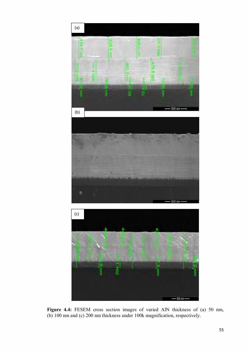
55
Figure 4.4: FESEM cross section images of varied AlN thickness of (a) 50 nm, (b) 100 nm and (c) 200 nm thickness under 100k magnification, respectively.
(a)
(b)
(c)

56
In order to justify the effect of varying the AlN nucleation layer on the surface
roughness and morphological properties of the topmost GaN layer, AFM surface imaging
was done on the sample. Table 4.3 shows the 2-dimensional (2D) and 3-dimensional (3D)
AFM images and properties of the topmost GaN layer at different AlN NL thickness.
Table 4.3: 2D, 3D images and the properties of topmost GaN layer with variation of AlN NL thickness.
AlN NL thickness (nm)
50 100 150
2-dimensional AFM image (5 × 5 µm2)
3-dimensional AFM image (5 × 5 µm2)
RMS Roughness (nm)
4.974 2.872 2.470
Peak to valley (nm)
11.028 8.782 7.712
Based on the results in the table above, the RMS roughness and the peak to valley
distance of the topmost GaN layer is significantly reduced. The surface of topmost GaN
layer becomes more coalescence as the AlN nucleation layer thickness is increased from
50 nm to 100 nm. At thickness of 50 nm, the topmost GaN layer exhibits a small granular
surface which contributes to higher surface roughness. Thus, the surface becomes
smoother as the thickness of AlN NL increase. The AlN sample coalesce properly during
growth and affects the smoothness of the top GaN layer. This effect is probably
contributed by low mobility of AlN during growth process. During initial growth phase,
AlN slowly forms during growth and slowly coalesce with time. However, it is extremely
challenging to achieve smooth GaN on AlN when the thickness of AlN becomes higher.
57
Luo et al. (2008) concluded that the optimum thickness that is achieved in his sample
is around 110 nm and the sample degrades as the AlN thickness is increased above 110
nm. In this research, however, the topmost GaN produce a smoother surface even after
the thickness is increased above 110 nm. This is probably due to high growth temperature
of AlN of 1000 °C which accommodate the movement of AlN molecules. Since AlN
coalesce more properly with the increase in AlN thickness, the peak to valley also slowly
reduces which indicates high quality behaviour of AlN. The ability to grow higher
thickness of AlN to produce an even better coalesce GaN layer highlights the potential of
HT-AlN layer to be the material template for high power applications.
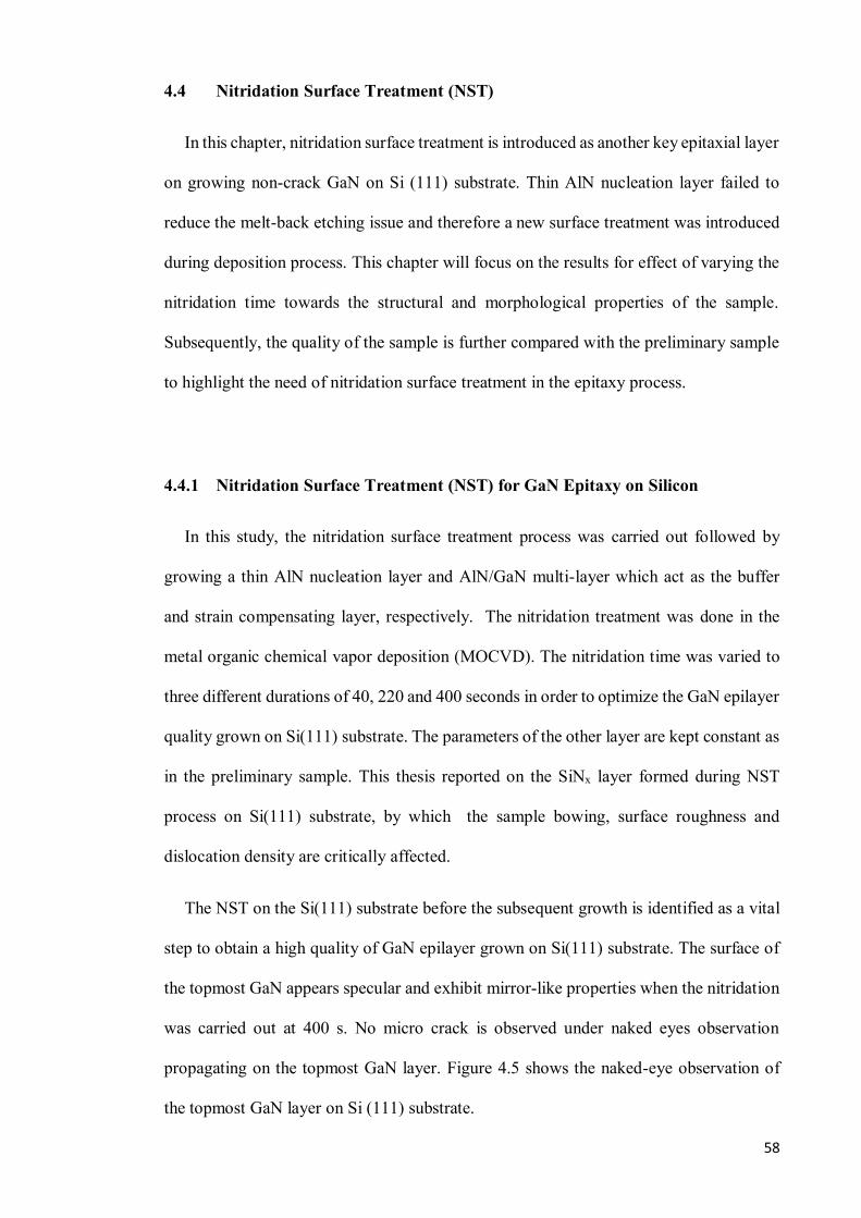
58
4.4 Nitridation Surface Treatment (NST)
In this chapter, nitridation surface treatment is introduced as another key epitaxial layer
on growing non-crack GaN on Si (111) substrate. Thin AlN nucleation layer failed to
reduce the melt-back etching issue and therefore a new surface treatment was introduced
during deposition process. This chapter will focus on the results for effect of varying the
nitridation time towards the structural and morphological properties of the sample.
Subsequently, the quality of the sample is further compared with the preliminary sample
to highlight the need of nitridation surface treatment in the epitaxy process.
4.4.1 Nitridation Surface Treatment (NST) for GaN Epitaxy on Silicon
In this study, the nitridation surface treatment process was carried out followed by
growing a thin AlN nucleation layer and AlN/GaN multi-layer which act as the buffer
and strain compensating layer, respectively. The nitridation treatment was done in the
metal organic chemical vapor deposition (MOCVD). The nitridation time was varied to
three different durations of 40, 220 and 400 seconds in order to optimize the GaN epilayer
quality grown on Si(111) substrate. The parameters of the other layer are kept constant as
in the preliminary sample. This thesis reported on the SiNx layer formed during NST
process on Si(111) substrate, by which the sample bowing, surface roughness and
dislocation density are critically affected.
The NST on the Si(111) substrate before the subsequent growth is identified as a vital
step to obtain a high quality of GaN epilayer grown on Si(111) substrate. The surface of
the topmost GaN appears specular and exhibit mirror-like properties when the nitridation
was carried out at 400 s. No micro crack is observed under naked eyes observation
propagating on the topmost GaN layer. Figure 4.5 shows the naked-eye observation of
the topmost GaN layer on Si (111) substrate.
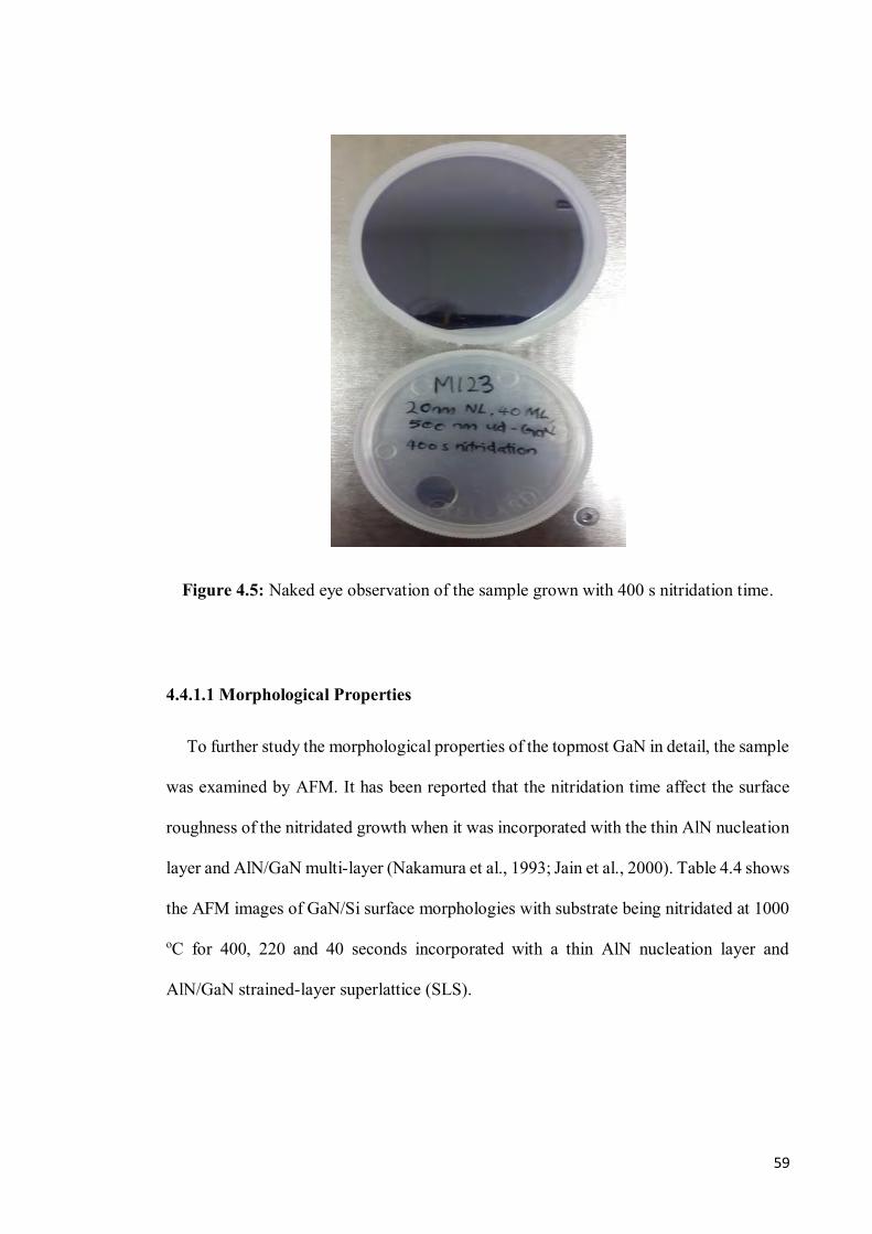
59
Figure 4.5: Naked eye observation of the sample grown with 400 s nitridation time.
4.4.1.1 Morphological Properties
To further study the morphological properties of the topmost GaN in detail, the sample
was examined by AFM. It has been reported that the nitridation time affect the surface
roughness of the nitridated growth when it was incorporated with the thin AlN nucleation
layer and AlN/GaN multi-layer (Nakamura et al., 1993; Jain et al., 2000). Table 4.4 shows
the AFM images of GaN/Si surface morphologies with substrate being nitridated at 1000
oC for 400, 220 and 40 seconds incorporated with a thin AlN nucleation layer and
AlN/GaN strained-layer superlattice (SLS).

60
Table 4.4: 3D, 2D images, the rms roughness and the peak to valley value of the topmost GaN layer at different nitridation duration of (a) 400 seconds, (b) 220 seconds and (c) 40 seconds, respectively.
As it can be seen in Table 4.4, the value of root mean square (RMS) roughness for the
top GaN epilayer is decreasing from 3.365 to 1.475 nm as the nitridation time was
increased from 40 to 400 s. The AFM images also proved that the top GaN epilayer was
found to be more uniform and homogenous compared to the others at 400 s of nitridation
time, with smallest grain size and peak to valley value at 4.247 nm. It has been reported
widely that a SiNx layer was formed prior to the NST process on the silicon substrate
(Ozturk et al., 2013; Pal & Jacob, 2004). This SiNx layer can improve the crystal quality
of the top GaN epilayer while efficiently prevented the substrate from any oxygen
diffusion and silicon gasing process from reacting with the gallium during the GaN
growth (Ozturk et al., 2013). Hence, it will oppose the melt-back etching issue (Ishikawa
et al., 1998; Ishikawa et al., 1999; Able et al., 2005). The GaN grains gradually coalesced
with reduction in cluster size, suggesting the transition in growth mode from three-
dimensional towards two-dimensional like growth (Wuu et al., 1999).

61
A high quality of GaN epilayers also can be produced through restraining the sample
bowing from the substrate during the epitaxial growth. It has been reported that the
substrate bowing could be compressed by inserting strained-layer superlattice as the strain
compensating layer in a particular growth structure (Aida et al., 2011). In this set, we
have applied a thin AlN nucleation layer and 40 pairs of AlN/GaN multi-layer to inherit
the former publications. Figure 4.6 shows the graph of wafer bowing of the sample against
different nitridation time.
Figure 4.6: Graph of wafer bowing (µm) against nitridation time (s).
From the plotted graph, it is observed that from range of 50 to 220 s, the bowing effect
on the silicon substrate greatly reduces from 82 µm to around 55 µm. This value is
expected as it was also been observed by Rowena et.al. (2011). It is found that the bowing
of the samples decreased as we increased the nitridation time, in which the lowest bowing
of 51.99 µm was recorded at 400 s of nitridation time. It is crucial to mention that the
compressive stress generated in the front-side surface of Si(111) substrate after growing
the GaN layer is greatly influenced by SiNx layer formed at 400 s of nitridation time. SiNx
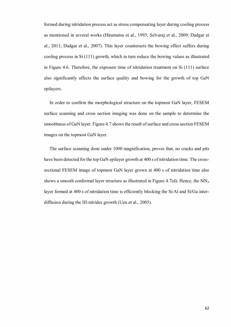
62
formed during nitridation process act as stress compensating layer during cooling process
as mentioned in several works (Hiramatsu et al., 1993; Selvaraj et al., 2009; Dadgar et
al., 2011; Dadgar et al., 2007). This layer counteracts the bowing effect suffers during
cooling process in Si (111) growth, which in turn reduce the bowing values as illustrated
in Figure 4.6. Therefore, the exposure time of nitridation treatment on Si (111) surface
also significantly affects the surface quality and bowing for the growth of top GaN
epilayers.
In order to confirm the morphological structure on the topmost GaN layer, FESEM
surface scanning and cross section imaging was done on the sample to determine the
smoothness of GaN layer. Figure 4.7 shows the result of surface and cross section FESEM
images on the topmost GaN layer.
The surface scanning done under 1000 magnification, proves that, no cracks and pits
have been detected for the top GaN epilayer growth at 400 s of nitridation time. The cross-
sectional FESEM image of topmost GaN layer grown at 400 s of nitridation time also
shows a smooth conformal layer structure as illustrated in Figure 4.7(d). Hence, the SiNx
layer formed at 400 s of nitridation time is efficiently blocking the Si/Al and Si/Ga inter-
diffusion during the III-nitrides growth (Uen et al., 2005).

63
Figure 4.7: The surface scanning images of GaN grown on Si(111) substrate at (a) 400 s, (b) 220 s and (c) 40 s of nitridation time and (d) the cross-sectional image of the GaN epitaxial growth on silicon (111) substrate at 400 s of nitridation time.
This results validated the NST process is crucial in order to sustain the tensile strain
on each heteroepitaxy layer. Thus, it can indirectly diminish the defect that commonly
occurred during the growth of GaN on silicon(111) substrate (Dadgar et al., 2000). These
results have concluded that a high quality of topmost GaN epilayer with a smooth and
fine epitaxial surface grown on Si(111) substrate is successfully achieved after the NST
process for 400 s nitridation time. In terms of generation of crack, the absence of melt-
back etching from efficient nitridation surface treatment prevents the formation of crack
in the sample as illustrated in Figure 4.7(a).
64
4.4.1.2 Structural Properties
Since the morphological results confirmed all the observations logically, the structural
quality of the topmost GaN layer have been observed using x-ray rocking curve (XRC)
measurement. The XRC (0002) analysis was performed to study the screw dislocation
while the XRC (101̅2) for the edge and mixed dislocation that occurred in the top GaN
epilayer (Arslan et al., 2009; Metzger et al., 1998). The graph obtained for both analyses
are presented in Figure 4.8(a) and (b).
The graph shows that the FWHM value for both analyses become narrower as the
nitridation time is increased. It can also be observed that the sample at 400 s of nitridation
time exhibits the lowest FWHM with 1126 arcsec for (0002) and 2012 arcsec for (101̅2)
measurement. The reductions of FWHM value as the nitridation time increased indicates
the reduction of dislocation density in the topmost GaN epilayer (Arslan et al., 2009;
Metzger et al., 1998). Si usually outgases during growth and produce dislocation sites as
Si reacts with Ga to produce gallium silicide. Nitridation surface treatment provides an
additional barrier which reduce the formation of gallium silicide, thus reducing the
dislocation density inside the sample. It can be concluded that NST technique under 400s
duration is effective towards blocking Si/Al and Si/Ga inter-diffusion during the III-
nitrides growth. This leads toward a perfect growth of AlN/GaN strained-layer
superlattice (SLS) as shown in Figure 4.7(d).
65
Figure 4.8: The XRC measurement of (a) (0002) and (b) (101̅2) scan of samples deposited at different nitridation time.
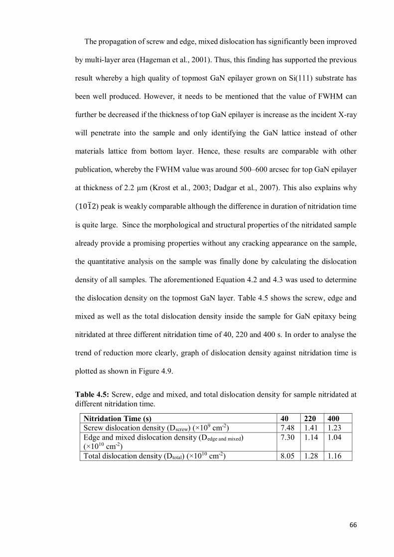
66
The propagation of screw and edge, mixed dislocation has significantly been improved
by multi-layer area (Hageman et al., 2001). Thus, this finding has supported the previous
result whereby a high quality of topmost GaN epilayer grown on Si(111) substrate has
been well produced. However, it needs to be mentioned that the value of FWHM can
further be decreased if the thickness of top GaN epilayer is increase as the incident X-ray
will penetrate into the sample and only identifying the GaN lattice instead of other
materials lattice from bottom layer. Hence, these results are comparable with other
publication, whereby the FWHM value was around 500–600 arcsec for top GaN epilayer
at thickness of 2.2 µm (Krost et al., 2003; Dadgar et al., 2007). This also explains why
(101̅2) peak is weakly comparable although the difference in duration of nitridation time
is quite large. Since the morphological and structural properties of the nitridated sample
already provide a promising properties without any cracking appearance on the sample,
the quantitative analysis on the sample was finally done by calculating the dislocation
density of all samples. The aforementioned Equation 4.2 and 4.3 was used to determine
the dislocation density on the topmost GaN layer. Table 4.5 shows the screw, edge and
mixed as well as the total dislocation density inside the sample for GaN epitaxy being
nitridated at three different nitridation time of 40, 220 and 400 s. In order to analyse the
trend of reduction more clearly, graph of dislocation density against nitridation time is
plotted as shown in Figure 4.9.
Table 4.5: Screw, edge and mixed, and total dislocation density for sample nitridated at different nitridation time.
Nitridation Time (s) 40 220 400 Screw dislocation density (Dscrew) (×109 cm-2) 7.48 1.41 1.23 Edge and mixed dislocation density (Dedge and mixed) (×1010 cm-2)
7.30 1.14 1.04
Total dislocation density (Dtotal) (×1010 cm-2) 8.05 1.28 1.16

67
Figure 4.9: The screw and edge, mixed dislocation density of samples deposited at different nitridation time.
From Figure 4.9, it can be distinctly observed that the lowest dislocation density was
achieved at 400s of nitridation time. The result is expected due to several supportive
reasons such as the specular, mirror-like surface of the sample, reduction in AFM
roughness and bowing effect possessed by the sample, crack-free surface as seen under
microscope and lastly, the reduction in FWHM of the sample being nitridated at 400 s.
Based on this basis, the necessity of nitridation surface treatment process to achieve
mirror-like surface GaN on Si (111) epitaxy is properly highlighted and deduced as one
of the key parameter to achieve high quality GaN on Si (111) substrate.

68
4.5 AlN/GaN Strained-Layer Superlattice (SLS)
In this chapter, AlN/GaN strained-layer superlattice (SLS) growth will be discussed as
another key parameter to grow non-crack GaN on Si (111) substrates. Chapter 4.5.1 will
briefly introduce the necessity of investigating the influence of AlN/GaN SLS for GaN
epitaxy on Si (111) substrates. The effect of manipulating the AlN/GaN SLS layer
parameter will be discussed in Chapter 4.5.2.
4.5.1 AlN/GaN SLS for Crack-free GaN Surface
While nitridation surface treatment (NST) acts as an epitaxial passivation layer for the
growth of polycrystalline GaSi during GaN growth as can be seen in previous chapter,
AlN/GaN SLS serves as dislocation buffer layer and functioned to reduce the higher
bowing effect of thicker GaN on Si (111). Driven by the motivation to achieve thicker
crack-free GaN on Si (111), the AlN/GaN SLS effect as dislocation filtering layer will be
described in detail throughout this chapter. The ability of AlN/GaN SLS in assisting
crack-free epitaxial GaN layer will also be discussed in this chapter. The large lattice and
thermal mismatch of AlN and GaN will create edge dislocation inside the lattice due to
incomplete and missing atomic arrangement inside the layer.
The conversion factor from AlN lattice to GaN lattice will usually create a gap in
between the lattice matching and introduce uncontrolled tensile stress on the GaN
epilayer. The effect increases towards thicker GaN layer until certain specific thickness
denoted as critical thickness where such effects generate cracking of GaN layer on Si due
to incapability of AlN to compensate higher generated tensile stress of GaN. It is well
known that dislocation and cracks will also deteriorates the device quality and generally
induce unwanted thermal accumulation inside the sample.

69
Owing to such reason, a strain compensating technology involving the usage of
AlN/GaN SLS have been introduced to compensate the strain and lead towards avoiding
crack issue on the sample. In an effort to properly investigate the effect of AlN/GaN SLS
layer towards diminishing crack issues on thicker GaN, the AlN/GaN SLS were grown at
4 different number of pairs while maintaining the parameter of other layers.
4.5.2 Effect of Varying the Aluminium Nitride/Gallium Nitride (AlN/GaN)
Strained-layer Superlattice (SLS) Pairs
Four different growth have been done to investigate the effect of AlN/GaN strained-
layer superlattice (SLS) towards achieving crack-free GaN on Si (111) substrates by
varying the number of AlN/GaN SLS pairs to 20, 40, 60 and 80 pairs. The efficiency of
AlN/GaN multilayer as dislocation filtering and defect annihilating layer to provide high
quality GaN epilayer is established by observing the quality of the topmost GaN layer.
4.5.2.1 Morphological Properties
In this work, to study the effect of varying AlN/GaN strain-layer superlattice (SLS)
periods on the surface quality of the GaN epitaxial layer, the sample was examined by
AFM. Table 4.6 shows the AFM images and the morphological properties in terms of
root mean square (RMS) roughness and peak-to-valley value of GaN deposited on top of
AlN/GaN SLS structure with varying periods of 20, 40, 60 and 80 pairs.
As stated in Table 4.6, the value of RMS roughness is decreasing as the number of
AlN/GaN SLS periods in the GaN structure increases from 20 to 60 pairs. At 80 periods
of AlN/GaN SLS, the RMS value slightly increase suggesting some sort of surface
degradation occurring in top GaN layer. Lowest peak-to-valley value was achieved for
70
sample with 60 periods of AlN/GaN SLS before a sudden increase of peak-to-valley in
sample at 80 AlN/GaN SLS. The coalescence process of AlN/GaN SLS is the vital
condition towards achieving crack-free topmost GaN layer. While sample with 60 periods
of AlN/GaN SLS effectively reduce the roughness of topmost GaN layer, sample at 80
periods of AlN/GaN SLS experience a deterioration in terms of roughness and peak to
valley value.
Valcheva et al. (2003) relates this behaviour towards the alternating
tensile/compressive strain within each period due to lattice mismatch between AlN and
GaN layers. The overall composition of AlN in the AlN/GaN SLS might also induced the
formation of island-like structure on the topmost GaN layer. It is deduced that for 80
periods of AlN/GaN SLS the 3D growth effect dominates the 2D growth which explains
the increase in peak to valley value from 4.8 nm to 7.9 nm. At the same time, the
roughness of GaN/Si also increases from 1.617 nm to 2.887 nm.

71
Table 4.6: Average roughness and peak to valley (P-V) of grown sample.
No. of AlN/GaN SLS pairs
3 Dimensional (3D) Image Average Roughness (RMS) (nm)
Peak to Valley (nm)
20
1.900 5.083
40
1.674 5.025
60
1.617 4.781
80
2.887 7.953

72
While bowing have been detected as one of the crucial parameter which controls the
cracking issues in GaN epilayer, an increase in the number of AlN/GaN SLS periods from
20 to 40 results in a decrease in bowing effect of the sample as can be seen in
Figure 4.10. However, an increment in bowing value was obtained from 65 µm to 100
µm as the periods of AlN/GaN SLS were increased from 40 to 60 pairs. Despite the
increase in bowing value, a crack-free top GaN layer was successfully achieved for
sample of 60 periods of AlN/GaN SLS.
The result obtained was against several reports which relates formation of high quality
GaN epilayers with lower bowing parameter during epitaxial growth
(Hiramatsu et al., 1993; Dadgar et al., 2011; Cheng et al., 2011; Sakai et al., 2004). The
possible explanation to this result lies on the epitaxial engineering behind the introduction
of AlN/GaN superlattice itself. During epitaxial growth, a large stress is induced due to
large lattice mismatch between AlN buffer layer and Si. The initial AlN nucleation layer
usually comprises of high dislocation density due to strain relaxation in the film. (Ubukata
et al., 2007). Introduction of AlN in SLS induces compressive stress to the subsequent
period of AlN/GaN SLS which counterbalances both the growth-induced tensile stress
and the thermally-induced tensile strain in SLS during cooling process.
The doping of Si in GaN is responsible in introduction of tensile stress in those layer,
although the substitution of Si for Ga only causes negligible changes in the lattice constant
(Cheng et al.,2011). The tensile increase explained the finding of crack in sample
inherited with 40 AlN/GaN SLS although the bowing of the overall structure was slightly
reduced as compared to 20 AlN/GaN SLS. Since the growth have been done under slight
doping of Si throughout the whole layer to increase the carrier mobility of buffer layer, it
is found that unintentionally Si-doping also increase the tensile effect on the topmost GaN
layer (Manning et al., 2010). Therefore, this clearly explaining the crack-free GaN
obtained despite that quite large bowing value as compared to many publications. It is

73
therefore concluded that under such Si doping, 60 pairs of ALN/GaN SLS was sufficient
to act as an effective dislocation barrier to produce crack-free GaN. Although the bowing
increment can be related to the total Al composition in the structure, much works shall be
done to support such basis.
Figure 4.10: Bowing against total thickness of sample.
To further confirm our observation, the samples were characterized using FESEM for
the top-view and the cross section images of our structure. Figure 4.11(a), (b), (c) and (d)
refer to the top-view image of FESEM under 10K magnification. The image shows
absence of cracks for the top-GaN epilayer growth at 60 periods of AlN/GaN SLS.
Several small pits were still present as indicated by the small arrow in Fig 4.11(c).
However, such pits did not contributes in the formation of cracks on the sample. The
cross-sectional image also shows fine, abrupt structure of AlN/GaN SLS at 60 periods as
illustrated in FESEM surface depicted by Figure 4.11(c). The results justified the crack-
free GaN that were obtained in the sample, thus relates the necessity of getting a fine SLS
structure which can effectively act as dislocation filtering layer.
74
Astonishingly, the crack reappears in sample deposited at 80 periods of AlN/GaN SLS.
The above observation supports the previous deduction that with higher aluminium to
overall AlN/GaN structure content, the surface quality deteriorates back and crack have
been generated back. With respect to AFM images, a clear outline was given that to
achieve a high quality crack free GaN epilayer with smooth and fine surface of topmost
GaN, the AlN/GaN SLS should be abrupt and fine with controlled, fixed thickness to
sustain the strain-stress counterbalance generated in AlN/Si interface during AlN/GaN
SLS growth.
Based on Figure 4.12(b), the AlN/GaN SLS interface is fine and abruptly formed with
uniform thickness. Thus, it is later concluded that the only reason in the increase of
bowing and deterioration of topmost GaN quality on sample deposited at 80 pairs of
AlN/GaN SLS was mainly due to the Al content in the overall structure. While for sample
deposited with 60 pairs of AlN/GaN SLS, the AlN introduced in the SLS structure
perfectly counterbalanced the tensile effect by inducing compressive stress in the
structure during cooling process to produce crack-free GaN on Si(111) substrates
(Cao et al., 2016).

75
Figure 4.11: FESEM surface of sample with different SLS pairs of (a) 20 pairs, (b) 40 pairs, (c) 60 pairs and (d) 80 pairs viewed under 10K magnification.

76
Figure 4.12: (a) Cross section image of overall structure under 100k magnification, and (b) Cross section image of multi-layer thickness under 200k magnification, respectively.
Based on Figure 4.12(b), the AlN/GaN SLS thickness was uniformly grown with a
precise thickness of 13.11 nm for GaN layer and 10.20 nm for AlN layer. Such thickness
contributed to the GaN and AlN growth rate of 0.49 nm/s and 0.70 nm/s, respectively.
77
4.5.2.2 Structural Properties
While the images of FESEM and AFM have already provide such understanding, XRC
analysis was carried out to further investigate the influence of varying the number of
periods of AlN/GaN SLS towards the structural properties of GaN grown on Si (111)
substrates. Two kinds of in-plane characterizations was done using XRC analysis on
(0002) and (101̅2) plane for the edge and mixed dislocation that happened in the top GaN
epilayer. The graph for both analyses are presented in Figure 4.13(a) and Figure 4.13(b).
The graph shows the narrowest FWHM value for sample deposited with 60 periods of
AlN/GaN SLS. Further increase in the number of periods of AlN/GaN SLS shows an
increase in both edge and mixed dislocation of the sample.
The reductions of FWHM value as the AlN/GaN SLS were increased, indicates the
reduction in dislocation density in the top GaN epilayer. Such results clearly shows the
function of AlN/GaN SLS to reduce and compensate the propagation of the screw, edge
and mixed dislocation in the sample (Hageman et al., 2001). However, it is compulsory
to mention that the value of FWHM can be further reduced if we increase the thickness
of top GaN epilayer since the incident x-ray will only detect the dislocation in the top
GaN epilayer instead of other layers. It is convinced that the FWHM that were obtained
comprises of the total dislocation in the AlN/GaN SLS and the top-GaN epilayer itself.
Several works also have reported that the threading dislocation might penetrates the
AlN/GaN SLS up to several hundred nanometres before completely terminated depending
on the composition and type of SLS materials. Hence, these results are comparable with
other publication, by which the FWHM value was around 500 to 600 arcsec for top GaN
epilayer at thickness of 2.2 µm (Dadgar et al., 2003; Krost et al., 2003).

78
Figure 4.13 (a) (0002) and (b) (101̅2) XRC scan for all samples deposited at different number of AlN/GaN SLS pairs.

79
While morphological and structural analysis already suggested 60 pairs of AlN/GaN
SLS as optimum periods to effectively reduce the dislocation density based on FWHM
result, numerical calculations have been made to confirm and obtain the figurative value.
The aforementioned Equations 4.2 and 4.3 was used to determine the dislocation density
on the topmost GaN layer. Table 4.7 shows the screw, edge and mixed, and the total
dislocation density value for the samples deposited at different AlN/GaN SLS periods of
20, 40, 60 and 80 pairs. In order to analyse the trend of reduction more clearly, graph of
dislocation density for screw and edge, mixed dislocation density against number of
AlN/GaN SLS pairs is plotted as shown in Figure 4.14.
Table 4.7: Screw, edge and mixed, and total dislocation density for sample deposited at different number of AlN/GaN SLS pairs.
No. of AlN/GaN SLS pairs 20 40 60 80 Screw dislocation density (Dscrew) (×109 cm-2) 12.60 2.87 2.45 2.70 Edge and mixed dislocation density (Dedge and mixed) (×1010 cm-2)
11.70 1.54 1.19 1.32
Total dislocation density (Dtotal) (×1010 cm-2) 13.0 1.83 1.44 1.59
Figure 4.14: The screw and edge, mixed dislocation density of samples deposited at different number of AlN/GaN SLS pairs.

80
From Figure 4.14, it can be clearly seen that the lowest screw and edge, mixed
dislocation was achieved using epitaxial technology involving growth with 60 pairs of
AlN/GaN SLS structure. The result is expected due to several supportive reasons such as
the reduction in AFM roughness and bowing effect possessed by the sample, crack-free
surface as seen under microscope and lastly, the reduction in FWHM of the sample being
grown using 60 pairs of AlN/GaN SLS structure.
Based on this basis, the effect of using AlN/GaN SLS to efficiently diminishing the
crack issues by manipulation of strain-stress interaction in between the heteroepitaxial
layers for GaN on Si (111) substrates have been successfully investigated. Thus, it is
concluded that 60 pairs of AlN/GaN SLS technology is the optimum parameter to
proficiently achieve 500 nm crack-free GaN epitaxy on Si(111) substrates provided that
the overall layer were slightly doped with Si and achieve a thickness ratio for AlN: GaN
that is approximately 10 nm: 13 nm.

81
CHAPTER 5: CONCLUSION
5.1 Introduction
This chapter will summarizes all the results and highlights several discussions that
have been stated in Chapter 4. The crucial explanation and significant results towards the
conclusion of this thesis will be properly arranged and presented in a systematic manner.
The contribution in terms of knowledge and understanding the crack-free growth of GaN
on Si (111) substrates will be emphasized. The objectives of the thesis will be properly
answered as to indicate the progression in epitaxial technology that have been fully
understood by the author. Chapter 5.2 will conclude this work and the current
understanding that the author have while Chapter 5.3 will outline the potential future work
to preserve the author’s motivation towards achieving high quality epitaxial GaN growth
on Si (111) substrates.
5.2 Conclusion
Throughout this whole work, a homogeneous, high temperature aluminium nitride
(HT-AlN) nucleation layer (NL) have been successfully grown on silicon (111) substrate.
The sample is specular at ALN NL thickness of 200 nm. AFM surface imaging provides
a RMS surface roughness of 2.470 nm and peak-to-valley value of 7.712 nm. From the
homogeneity test, high temperature AlN (HT-AlN) NL was successfully grown on silicon
(111) substrate with better HT-AlN NL quality at higher thickness of 200nm. Although
preliminary optimization on the AlN thickness shows positive trend towards higher
thickness of nucleation layer, in term of device performance, lower AlN NL thickness
dictates favourable result with higher device conductivity.
Driven towards this goal, enhanced epitaxial technology involving the usage of
nitridation and AlN/GaN strained-layer superlattice (SLS) has been employed to

82
compensate thinner AlN NL properties towards achieving high quality crack-free GaN
epitaxy on Si (111) substrate.
Subsequently, the effect of varying the nitridation surface treatment (NST) time with
the quality of topmost GaN layer have been successfully investigated. The best topmost
GaN quality was achieved at 400s with specular Si surface as seen by bare eyes. Further
characterization on AFM reveals the lowest RMS roughness of 1.475 nm and peak-to-
valley value of 4.247 nm. With an increment in NST time, lower bowing effect was
achieved on the sample with the lowest one recorded at 51.99 µm. FESEM images reveal
a crack-free 500 nm GaN surface deposited at NST of 400s was achieved when being
characterized using FESEM which confirmed our objective. Lowest FWHM was
achieved at 1126 and 2012 arcsec for in-plane characterization at (002) and (102),
respectively. Numerical calculation displays lowest dislocation density of 1.23 × 10⁹ and
1.04 × 1010 cm-2 for screw and edge, mixed dislocation density.
Next, an optimum 60 pairs of AlN/GaN strained-layer superlattice (SLS) was
employed to achieve a 1µm crack-free GaN growth on is (111) substrate. The lowest
RMS roughness and a peak-to-valley value of 1.617 nm and 4.781 nm, respectively was
achieved with fine, abrupt SLS structure as depicted in FESEM cross section images. The
AlN/GaN SLS thickness was uniformly grown with a precise thickness of 13.11 nm for
GaN layer and 10.20 nm for AlN layer. Such thickness contributed to the GaN and AlN
growth rate of 0.49 nm/s and 0.70 nm/s, respectively. XRC analysis produces the lowest
FWHM of 1103 and 1497 for (002) and (102) in-plane characterization, respectively. In
addition, numerical calculation for screw and edge, mixed dislocation shows the lowest
value at 2.45 × 10⁹ and 1.19 × 10¹⁰, respectively.
Thus, it is concluded that 60 pairs of AlN/GaN SLS technology is the optimum
parameter to proficiently achieve 1µm crack-free GaN epitaxy on Si(111) substrates
provided that the overall layer were slightly doped with Si and achieve a thickness ratio
83
for AlN: GaN that is approximately 10 nm:13 nm. Therefore, a crack-free GaN layer have
been successfully grown on silicon (111) substrates.
5.3 Suggested Potential Future Works
Due to the achievement throughout this thesis, several potential future works can be
highlighted to further understand the behavioural change of NST and SLS epitaxial
technology for GaN growth on Si (111) substrates. The potential future works as
suggested are:
1. Structural and morphological optimization of AlN/GaN SLS thickness to
understand the effect of changing Al composition towards the overall SLS
structure.
2. Optimization of Si-doped AlN/GaN SLS to achieve smoother and better quality
of topmost GaN layer.
3. LED epitaxy optimization on Si (111) substrate due to cheaper substrate value and
higher potential of silicon to be integrated with current semiconductor technology.

84
REFERENCES
Able, A., Wegscheider, W., Engl, K., & Zweck, J. (2005). Growth of crack-free GaN on Si (111) with graded AlGaN buffer layers. Journal of Crystal Growth, 276(3), 415-418.
Able, A., Wegscheider, W., Engl, K., & Zweck, J. (2005). Growth of crack-free GaN on Si (111) with graded AlGaN buffer layers. Journal of Crystal Growth, 276(3), 415-418.
Aida, H., Takeda, H., Aota, N., & Koyama, K. (2011). Reduction of bowing in GaN-on-sapphire and GaN-on-silicon substrates by stress implantation by internally focused laser processing. Japanese Journal of Applied Physics, 51(1R), 016504.
Ambacher, O., Majewski, J., Miskys, C., Link, A., Hermann, M., Eickhoff, M., Stutzmann, M., Bernardini, F., Fiorentini, V., Tilak, V. & Schaff, B. (2002). Pyroelectric properties of Al(In)GaN/GaN hetero-and quantum well structures. Journal of Physics: Condensed Matter, 14(13), 3399.
Arslan, E., Ozturk, M. K., Duygulu, Ö., Kaya, A. A., Ozcelik, S., & Ozbay, E. (2009). The influence of nitridation time on the structural properties of GaN grown on Si (111) substrate. Applied Physics A: Materials Science & Processing, 94(1), 73-82.
Arslan, E., Ozturk, M. K., Teke, A., Ozcelik, S., & Ozbay, E. (2008). Buffer optimization for crack-free GaN epitaxial layers grown on Si (1 1 1) substrate by MOCVD. Journal of Physics D: Applied Physics, 41(15), 155317.
As, D. J., Potthast, S., Fernandez, J., Lischka, K., Nagasawa, H., & Abe, M. (2006). Cubic GaN/AlGaN Schottky-barrier devices on 3C-SiC substrates. Microelectronic Engineering, 83(1), 34-36.
Bachman, M. (1999). RCA-1 silicon wafer cleaning. INRF application note Engineering of Microworld at the University of California. Irvine.
Bai, J., Dudley, M., Sun, W. H., Wang, H. M., & Khan, M. A. (2006). Reduction of threading dislocation densities in AlN∕ sapphire epilayers driven by growth mode modification. Applied Physics Letters, 88(5), 051903.
85
Bläsing, J., Reiher, A., Dadgar, A., Diez, A., & Krost, A. (2002). The origin of stress reduction by low-temperature AlN interlayers. Applied Physics Letters, 81(15), 2722-2724.
Bourret, A., Adelmann, C., Daudin, B., Rouvière, J. L., Feuillet, G., & Mula, G. (2001). Strain relaxation in (0001) AlN/GaN heterostructures. Physical Review B, 63(24), 245307.
Cao, Y., Laboutin, O., Johnson, W., Ganguly, S., Xing, G., & Jena, D. (2016). Epitaxy of GaN on Silicon. Thin Films on Silicon: Electronic and Photonic Applications, 8, 79.
Chandrasekhar, D., Smith, D. J., Strite, S., Lin, M. E., & Morkoç, H. (1995). Characterization of Group III-nitride semiconductors by high-resolution electron microscopy. Journal of Crystal Growth, 152(3), 135-142.
Cheng, K., Liang, H., Van Hove, M., Geens, K., De Jaeger, B., Srivastava, P., Kang, X., Favia, P., Bender, H., Decoutere, S. & Dekoster, J. (2011). AlGaN/GaN/AlGaN double heterostructures grown on 200 mm silicon (111) substrates with high electron mobility. Applied Physics Express, 5(1), 011002.
Cho, S. J., & Boo, J. H. (2012). A study on the characteristics of plasma polymer thin film with controlled nitrogen flow rate. Nanoscale Research Letters, 7(1), 62.
Dadgar, A., Bläsing, J., Diez, A., & Krost, A. (2011). Crack-free, highly conducting GaN layers on Si substrates by Ge doping. Applied Physics Express, 4(1), 011001.
Dadgar, A., Bläsing, J., Diez, A., Alam, A., Heuken, M., & Krost, A. (2000). Metalorganic chemical vapor phase epitaxy of crack-free GaN on Si (111) exceeding 1 µm in thickness. Japanese Journal of Applied Physics, 39(11B), L1183.
Dadgar, A., Poschenrieder, M., Bläsing, J., Contreras, O., Bertram, F., Riemann, T., Reiher, A., Kunze, M., Daumiller, I., Krtschil, A. & Diez, A. (2003). MOVPE growth of GaN on Si (111) substrates. Journal of Crystal Growth, 248, 556-562.
Dadgar, A., Poschenrieder, M., Bläsing, J., Fehse, K., Diez, A., & Krost, A. (2002). Thick, crack-free blue light-emitting diodes on Si (111) using low-temperature AlN interlayers and in situ SixNy masking. Applied Physics Letters, 80(20), 3670-3672.
86
Dadgar, A., Veit, P., Schulze, F., Bläsing, J., Krtschil, A., Witte, H., Diez, A., Hempel, T., Christen, J., Clos, R. & Krost, A. (2007). MOVPE growth of GaN on Si–Substrates and strain. Thin Solid Films, 515(10), 4356-4361.
Dhakal, D., Assim, K., Lang, H., Bruener, P., Grehl, T., Georgi, C., Waechtler, T., Ecke, R., Schulz, S. E. & Gessner, T. (2016). Atomic layer deposition of ultrathin Cu2O and subsequent reduction to Cu studied by in situ x-ray photoelectron spectroscopy. Journal of Vacuum Science & Technology A: Vacuum, Surfaces, and Films, 34(1), 01A111.
Domen, V. K. V. H. V. (1998). GaN-based blue laser diodes grown on SiC substrate as light source of high-density optical data storage. Fujitsu Scientific & Technical Journal, 34(2), 191-203.
Edmond, J., Abare, A., Bergman, M., Bharathan, J., Bunker, K. L., Emerson, D., Haberern, K., Ibbetson, J., Leung, M., Russel, P. & Slater, D. (2004). High efficiency GaN-based LEDs and lasers on SiC. Journal of Crystal Growth, 272(1), 242-250.
Egawa, T., Zhang, B., & Ishikawa, H. (2005). High performance of InGaN LEDs on (111) silicon substrates grown by MOCVD. IEEE Electron Device Letters, 26(3), 169-171.
Fujieda, S., Mizuta, M., & Matsumoto, Y. (1987). Growth characterization of low-temperature MOCVD GaN–comparison between N2H4 and NH3–. Japanese Journal of Applied Physics, 26(12R), 2067.
Gates, S. M., & Neumayer, D. A. (2001). U.S. Patent No. 6,203,613. Washington, DC: U.S. Patent and Trademark Office.
Gerthsen, D., Neubauer, B., Dieker, C., Lantier, R., Rizzi, A., & Lüth, H. (1999). Molecular beam epitaxy (MBE) growth and structural properties of GaN and AlN on 3C-SiC (001) substrates. Journal of Crystal Growth, 200(3), 353-361.
Gian, W., Skowronski, M., & Rohrer, G. S. (1996). Structural defects and their relationship to nucleation of GaN thin films. MRS Online Proceedings Library Archive, 423.
Haffouz, S., Grzegorczyk, A., Hageman, P. R., Vennégu, P., Van der Drift, E. W. J. M., & Larsen, P. K. (2003). Structural properties of maskless epitaxial lateral overgrown MOCVD GaN layers on Si (111) substrates. Journal of Crystal Growth, 248, 568-572.

87
Hageman, P. R., Haffouz, S., Kirilyuk, V., Grzegorczyk, A., & Larsen, P. K. (2001). High quality GaN layers on Si (111) substrates: AlN buffer layer optimisation and insertion of a SiN intermediate layer. Physica Status Solidi A Applied Research, 188(1/2), 523-526.
Hashimoto, S. (2006). Y. Yoshizumi, T. Tanabe, and M. Kiyama. Journal of Crystal Growth, 298, 871.
Hikosaka, T., Yoshida, H., Sugiyama, N., & Nunoue, S. (2014). Reduction of threading dislocation by recoating GaN island surface with SiN for high‐efficiency GaN‐
on‐Si‐based LED. Physica Status Solidi (c), 11(3‐4), 617-620.
Hiramatsu, K., Detchprohm, T., & Akasaki, I. (1993). Relaxation mechanism of thermal stresses in the heterostructure of GaN grown on sapphire by vapor phase epitaxy. Japanese Journal of Applied Physics, 32(4R), 1528.
Hofstetter, D., Baumann, E., Giorgetta, F. R., Graf, M., Maier, M., Guillot, F., Bellet-Amalric, E. & Monroy, E. (2006). High-quality AlN/GaN-superlattice structures for the fabrication of narrow-band 1.4 μm photovoltaic intersubband detectors. Applied Physics Letters, 88(12), 112-121.
Humphreys, T. P., Sukow, C. A., Nemanich, R. J., Posthill, J. B., Rudder, R. A., Hattangady, S. V., & Markunas, R. J. (1989). Microstructural and optical characterization of GaN films grown by PECVD on (0001) sapphire substrates. In MRS Proceedings (Vol. 162, p. 531). Cambridge University Press.
Ishikawa, H., Yamamoto, K., Egawa, T., Soga, T., Jimbo, T., & Umeno, M. (1998). Thermal stability of GaN on (111) Si substrate. Journal of Crystal Growth, 189, 178-182.
Ishikawa, H., Zhao, G. Y., Nakada, N., Egawa, T., Jimbo, T., & Umeno, M. (1999). GaN on Si substrate with AlGaN/AlN intermediate layer. Japanese Journal of Applied Physics, 38(5A), L492.
Jain, S. C., Willander, M., Narayan, J., & Overstraeten, R. V. (2000). III–nitrides: Growth, characterization, and properties. Journal of Applied Physics, 87(3), 965-1006.
Jasinski, J., Liliental-Weber, Z., Paduano, Q. S., & Weyburne, D. W. (2003). Inversion domains in AlN grown on (0001) sapphire. Applied Physics Letters, 83(14), 2811-2813.
88
Johnson, M. A. L., Fujita, S., Rowland Jr, W. H., Bowers, K. A., Hughes, W. C., He, Y. W., ... & Edmond, J. A. (1996). Molecular beam epitaxy growth and properties of GaN, Al x Ga1− x N, and AlN on GaN/SiC substrates. Journal of Vacuum Science & Technology B: Microelectronics and Nanometer Structures Processing, Measurement, and Phenomena, 14(3), 2349-2353.
Jones, A. C., & Hitchman, M. L. (2008). Overview of chemical vapour deposition. Chemical Vapour Deposition: Precursors, Processes and Applications, 1-36.
Jones, K. A., & Batyrev, I. G. (2012). The structure of dislocations in (In, Al, Ga) N wurtzite films grown epitaxially on (0001) or (112) GaN or AlN substrates. Journal of Applied Physics, 112(11), 113507.
Kim, M. H., Do, Y. G., Kang, H. C., Noh, D. Y., & Park, S. J. (2001). Effects of step-graded AlxGa1− xN interlayer on properties of GaN grown on Si (111) using ultrahigh vacuum chemical vapor deposition. Applied Physics Letters, 79(17), 2713-2715.
Kordoš, P., Bernát, J., Marso, M., Lüth, H., Rampazzo, F., Tamiazzo, G., Pierobon, R. & Meneghesso, G. (2005). Influence of gate-leakage current on drain current collapse of unpassivated GaN∕AlGaN∕GaN high electron mobility transistors. Applied Physics Letters, 86(25), 253511.
Krost, A., & Dadgar, A. (2002). GaN‐Based Devices on Si. Physica Status Solidi (a), 194(2), 361-375.
Krost, A., Dadgar, A., Strassburger, G., & Clos, R. (2003). GaN‐based epitaxy on silicon: stress measurements. Physica Status Solidi (a), 200(1), 26-35.
Krost, A., Schulze, F., Dadgar, A., Strassburger, G., Haberland, K., & Zettler, T. (2005). Simultaneous measurement of wafer curvature and true temperature during metalorganic growth of group‐III nitrides on silicon and sapphire. physica status solidi (b), 242(13), 2570-2574.
Lahreche, H., Vennéguès, P., Tottereau, O., Laügt, M., Lorenzini, P., Leroux, M., ... & Gibart, P. (2000). Optimisation of AlN and GaN growth by metalorganic vapour-phase epitaxy (MOVPE) on Si (111). Journal of Crystal Growth, 217(1), 13-25.
Lebedev, V., Cimalla, V., Kaiser, U., Foerster, C., Pezoldt, J., Biskupek, J., & Ambacher, O. (2005). Effect of nanoscale surface morphology on the phase stability of 3C-AlN films on Si (111). Journal of Applied Physics, 97(11), 114306.

89
Lebedev, V., Morales, F. M., Romanus, H., Krischok, S., Ecke, G., Cimalla, V., Himmerlich, M., Stauden, T., Cengher, D. & Ambacher, O. (2005). The role of Si as surfactant and donor in molecular-beam epitaxy of AlN. Journal of Applied Physics, 98(9), 093508.
Lei, T., Fanciulli, M., Molnar, R. J., Moustakas, T. D., Graham, R. J., & Scanlon, J. (1991). Epitaxial growth of zinc blende and wurtzitic gallium nitride thin films on (001) silicon. Applied Physics Letters, 59(8), 944-946.
Li, J., Nam, K. B., Nakarmi, M. L., Lin, J. Y., Jiang, H. X., Carrier, P., & Wei, S. H. (2003). Band structure and fundamental optical transitions in wurtzite AlN. Applied Physics Letters, 83(25), 5163-5165.
Liaw, H. M., Venugopal, R., Wan, J., Doyle, R., Fejes, P. L., & Melloch, M. R. (2000). GaN epilayers grown on 100 mm diameter Si (111) substrates. Solid-State Electronics, 44(4), 685-690.
Liu, L., & Edgar, J. H. (2002). Substrates for gallium nitride epitaxy. Materials Science and Engineering: R: Reports, 37(3), 61-127.
Lorenz, K., Gonsalves, M., Kim, W., Narayanan, V., & Mahajan, S. (2000). Comparative study of GaN and AlN nucleation layers and their role in growth of GaN on sapphire by metalorganic chemical vapor deposition. Applied Physics Letters, 77(21), 3391-3393.
Lozano, J. G., Morales, F. M., Garcia, R., González, D., Lebedev, V., Wang, C. Y., Cimalla, V. & Ambacher, O. (2007). Cubic InN growth on sapphire (0001) using cubic indium oxide as buffer layer. Applied Physics Letters, 90(9), 091901.
Luo, W., Wang, X., Guo, L., Xiao, H., Wang, C., Ran, J., ... & Li, J. (2008). Influence of AlN buffer layer thickness on the properties of GaN epilayer on Si (111) by MOCVD. Microelectronics Journal, 39(12), 1710-1713.
Madhu, M., Tegueu, A. M. K., Awaah, M., Wang, D., Park, M., Walker, F. J., & Kumar, D. K. (2005). Electrical Characterization of Blue Light Emitting Diodes as a Function of Temperature. In MRS Proceedings (Vol. 892, pp. 0892-FF12). Cambridge University Press.
Manasevit, H. M., & Simpson, W. I. (1971). The use of metal‐organics in the preparation of semiconductor materials II. II–VI compounds. Journal of The Electrochemical Society, 118(4), 644-647.

90
Manasreh, M. O. (1996). Optical absorption near the band edge in GaN grown by metalorganic chemical-vapor deposition. Physical Review B, 53(24), 16425.
Manning, I. C., Weng, X., Fanton, M. A., Snyder, D. W., & Redwing, J. M. (2010). Effects of composition on dislocation microstructure and stress in Si-doped AlxGa1− xN. Journal of Crystal Growth, 312(8), 1301-1306.
Marx, D., Kawazu, Z., & Hayafuji, N. (1998). U.S. Patent No. 5,760,426. Washington, DC: U.S. Patent and Trademark Office.
Matocha, K., Chow, T. P., & Gutmann, R. J. (2005). High-voltage normally off GaN MOSFETs on sapphire substrates. IEEE Transactions on Electron Devices, 52(1), 6-10.
Maula, J., Härkönen, K., & Nikolov, A. (2011). U.S. Patent No. 7,901,736. Washington, DC: U.S. Patent and Trademark Office.
Meng, J., Jaluria, Y., & Wong, S. (2013, December). Fabrication of GaN Films in a Chemical Vapor Deposition Reactor. In ASME 2013 4th International Conference on Micro/Nanoscale Heat and Mass Transfer (pp. V001T07A001-V001T07A001). American Society of Mechanical Engineers.
Metzger, T., Höpler, R., Born, E., Ambacher, O., Stutzmann, M., Stömmer, R., Schuster, M., Göbel, H., Christiansen, S., Albrecht, M. & Strunk, H. P. (1998). Defect structure of epitaxial GaN films determined by transmission electron microscopy and triple-axis X-ray diffractometry. Philosophical Magazine A, 77(4), 1013-1025.
Molnar, R. J., Götz, W., Romano, L. T., & Johnson, N. M. (1997). Growth of gallium nitride by hydride vapor-phase epitaxy. Journal of Crystal Growth, 178(1-2), 147-156.
Morkoc, H. (2013). Nitride semiconductors and devices (Vol. 32). Springer Science & Business Media.
Nagendra, B. S. (2009). MOCVD of Metal Nitride Thin Films : Deposition, Film Characteristics and Functional Properties (doctoral dissertation). Ruhr-University Bochum, Germany.
Nakamura, S., Pearton, S., & Fasol, G. (2013). The blue laser diode: the complete story. Springer Science & Business Media.
91
Nakamura, S., Senoh, M., & Mukai, T. (1993). High‐power InGaN/GaN double‐
heterostructure violet light emitting diodes. Applied Physics Letters, 62(19), 2390-2392.
Neugebauer, J. (2001). Ab initio Analysis of Surface Structure and Adatom Kinetics of Group‐III Nitrides. Physica Status Solidi (b), 227(1), 93-114.
Ni, Y., He, Z., Yang, F., Zhou, D., Yao, Y., Zhou, G., ... & Zhang, B. (2014). Effect of AlN/GaN superlattice buffer on the strain state in GaN-on-Si (111) system. Japanese Journal of Applied Physics, 54(1), 015505.
Nikishin, S. A., Faleev, N. N., Antipov, V. G., Francoeur, S., Grave de Peralta, L., Seryogin, G. A., Temkin, H., Prokofyeva, T. I., Holtz, M. & Chu, S. N. G. (1999). High quality GaN grown on Si (111) by gas source molecular beam epitaxy with ammonia. Applied Physics Letters, 75(14), 2073-2075.
Ozturk, M. K., Arslan, E., Kars, İ., Ozcelik, S., & Ozbay, E. (2013). Strain analysis of the GaN epitaxial layers grown on nitridated Si (111) substrate by metal organic chemical vapor deposition. Materials Science in Semiconductor Processing, 16(1), 83-88.
Pal, S., & Jacob, C. (2004). Silicon—a new substrate for GaN growth.Bulletin of Materials Science, 27(6), 501-504.
Pinna, N., Knez, M. & Editors. (2012). Atomic Layer Deposition of Nanostructured Materials. Wiley-VCH Verlag GmbH & Co. KGaA.
Rockett, A. (2007). The materials science of semiconductors. Springer Science & Business Media.
Romano, L. T., & Myers, T. H. (1997). The influence of inversion domains on surface morphology in GaN grown by molecular beam epitaxy. Applied Physics Letters, 71(24), 3486-3488.
Rosner, S. J., Carr, E. C., Ludowise, M. J., Girolami, G., & Erikson, H. I. (1997). Correlation of cathodoluminescence inhomogeneity with microstructural defects in epitaxial GaN grown by metalorganic chemical-vapor deposition. Applied Physics Letters, 70(4), 420-422.
Rowena, I. B., Selvaraj, S. L., & Egawa, T. (2011). Buffer thickness contribution to suppress vertical leakage current with high breakdown field (2.3 MV/cm) for GaN on Si. IEEE Electron Device Letters, 32(11), 1534-1536.

92
Sakai, A., Sunakawa, H., & Usui, A. (1998). Transmission electron microscopy of defects in GaN films formed by epitaxial lateral overgrowth. Applied Physics Letters, 73(4), 481-483.
Sakai, M., Egawa, T., Hao, M., & Ishikawa, H. (2004). Effect of various interlayers on epiwafer bowing in AlGaN/GaN high-electron-mobility transistor structures. Japanese Journal of Applied Physics, 43(12R), 8019.
Sakai, S., Kurai, S., Nishino, K., Wada, K., Sato, H., & Naoi, Y. (1996). Growth of GaN by sublimation technique and homoepitaxial growth by MOCVD. In MRS Proceedings (Vol. 449, p. 15). Cambridge University Press.
Schubert, E. F., Gessmann, T., & Kim, J. K. (2005). Light emitting diodes. Troy, NY: Cambridge University Press.
Seidl, H., Gutsche, M., Schroeder, U., Birner, A., Hecht, T., Jakschik, S., Luetzen, J., Kerber, M., Kudelka, S., Popp, T. & Orth, A. (2002, December). A fully integrated Al2O3 trench capacitor DRAM for sub-100 nm technology. In Electron Devices Meeting, 2002. IEDM'02. International (pp. 839-842). IEEE.
Selvaraj, S. L., Suzue, T., & Egawa, T. (2009). Breakdown enhancement of AlGaN/GaN HEMTs on 4-in silicon by improving the GaN quality on thick buffer layers. IEEE Electron Device Letters, 30(6), 587-589.
Shan, W., Schmidt, T. J., Yang, X. H., Hwang, S. J., Song, J. J., & Goldenberg, B. (1995). Temperature dependence of interband transitions in GaN grown by metalorganic chemical vapor deposition. Applied Physics Letters, 66(8), 985-987.
Shul, R. J., & Pearton, S. J. (Eds.). (2011). Handbook of advanced plasma processing techniques. Springer Science & Business Media.
[Side inlet design illustration]. Retrieved Mac 3, 2017 from https://www.mathesongas.com/electronics/mocvd-systems
Stutzmann, M., Ambacher, O., Eickhoff, M., Karrer, U., Lima Pimenta, A., Neuberger, R., ... & Grober, R. D. (2001). Playing with polarity. Physica Status Solidi (b), 228(2), 505-512.

93
Su, J., Armour, E. A., Krishnan, B., Lee, S. M., & Papasouliotis, G. D. (2015). Stress engineering with AlN/GaN superlattices for epitaxial GaN on 200 mm silicon substrates using a single wafer rotating disk MOCVD reactor. Journal of Materials Research, 30(19), 2846-2858.
Sugahara, T., Sato, H., Hao, M., Naoi, Y., Kurai, S., Tottori, S., ... & Sakai, S. (1998). Direct evidence that dislocations are non-radiative recombination centers in GaN. Japanese journal of applied physics, 37(4A), L398.
Takahashi, K., Yoshikawa, A., & Sandhu, A. (2007). Wide bandgap semiconductors (pp. 393-400). Berlin: Springer.
Thapa, S. B. (2010). Studies of AlN grown by MOVPE for electronic and optoelectronic applications (doctoral dissertation). Ulm University, Ulm, Germany.
Torvik, J. T., Leksono, M., Pankove, J. I., Van Zeghbroeck, B., Ng, H. M., & Moustakas, T. D. (1998). Electrical characterization of GaN/SiC np heterojunction diodes. Applied Physics Letters, 72(11), 1371-1373.
Tran, C. A., Osinski, A., Karlicek Jr, R. F., & Berishev, I. (1999). Growth of InGaN/GaN multiple-quantum-well blue light-emitting diodes on silicon by metalorganic vapor phase epitaxy. Applied Physics Letters, 75(11), 1494-1496.
Ubukata, A., Ikenaga, K., Akutsu, N., Yamaguchi, A., Matsumoto, K., Yamazaki, T., & Egawa, T. (2007). GaN growth on 150-mm-diameter (111) Si substrates. Journal of Crystal Growth, 298(2), 198-201.
Uen, W. Y., Li, Z. Y., Lan, S. M., & Liao, S. M. (2005). Epitaxial growth of high-quality GaN on appropriately nitridated Si substrate by metal organic chemical vapor deposition. Journal of Crystal Growth, 280(3), 335-340.
Valcheva, E., Paskova, T., Radnoczi, G. Z., Hultman, L., Monemar, B., Amano, H., & Akasaki, I. (2003). Growth-induced defects in AlN/GaN superlattices with different periods. Physica B: Condensed Matter, 340, 1129-1132.
Watanabe, A., Takeuchi, T., Hirosawa, K., Amano, H., Hiramatsu, K., & Akasaki, I. (1993). The growth of single crystalline GaN on a Si substrate using AIN as an intermediate layer. Journal of Crystal Growth, 128(1-4), 391-396.
94
Weimann, N. G., Eastman, L. F., Doppalapudi, D., Ng, H. M., & Moustakas, T. D. (1998). Scattering of electrons at threading dislocations in GaN. Journal of Applied Physics, 83(7), 3656-3659.
Wiest, F., Capodieci, V., Blank, O., Gutsche, M., Schulze, J., Eisele, I., Matusche, J. & Schmidt, U. I. (2006). Conformal aluminum oxide coating of high aspect ratio structures using metalorganic chemical vapor deposition. Thin Solid Films, 496(2), 240-246.
Wu, X. H., Kapolnek, D., Tarsa, E. J., Heying, B., Keller, S., Keller, B. P., Mishra, U. K., DenBaars S. P. & Speck, J. S. (1996). Nucleation layer evolution in metal‐organic chemical vapor deposition grown GaN. Applied Physics Letters, 68(10), 1371-1373.
Wuu, D. S., Tseng, W. H., Lin, W. T., & Horng, R. H. (1999). Influences of nitridation and thermal annealing on GaN buffer layers and the property of subsequent GaN epilayers grown by MOCVD. Surfaces and Vacuum, 1(9), 26-29.
Yang, T., Uchida, K., Mishima, T., Kasai, J., & Gotoh, J. (2000). Control of initial nucleation by reducing the V/III ratio during the early stages of GaN growth. Physica Status Solidi (a), 180(1), 45-50.
Ye, P. D., Wilk, G. D., Kwo, J., Yang, B. A. Y. B., Gossmann, H. J., Frei, M. A. F. M., Chu, S. N. G., Mannaerts, J. P., Sergent, M. A. S. M., Hong, M. A. H. M. & Ng, K. K. (2003). GaAs MOSFET with oxide gate dielectric grown by atomic layer deposition. IEEE Electron Device Letters, 24(4), 209-211.
Zamir, S., Meyler, B., Zolotoyabko, E., & Salzman, J. (2000). The effect of AlN buffer layer on GaN grown on (111)-oriented Si substrates by MOCVD. Journal of Crystal Growth, 218(2), 181-190.
Zang, K. Y., Wang, L. S., Chua, S. J., & Thompson, C. V. (2004). Structural analysis of metalorganic chemical vapor deposited AIN nucleation layers on Si (111). Journal of Crystal Growth, 268(3), 515-520.
Zhe, L., Xiao-Liang, W., Jun-Xi, W., Guo-Xin, H., Lun-Chun, G., & Jin-Min, L. (2007). The influence of AlN/GaN superlattice intermediate layer on the properties of GaN grown on Si (111) substrates. Chinese Physics, 16(5), 1467.
Zheng, X. H., Chen, H., Yan, Z. B., Han, Y. J., Yu, H. B., Li, D. S., ... & Zhou, J. M. (2003). Determination of twist angle of in-plane mosaic spread of GaN films by high-resolution X-ray diffraction. Journal of Crystal Growth, 255(1), 63-67.

95
Zhu, Y. (2012). Study on performance improvement of GaN-based light emitting diodes grown on silicon (111) substrates (doctoral dissertation). Retrieved from http://repo.lib.nitech.ac.jp.

96
LIST OF PUBLICATION AND PAPER PRESENTED
Publication
1. Rahman, M. N. A., Yusuf, Y., Mansor, M., & Shuhaimi, A. (2016). Effect of
nitridation surface treatment on silicon (111) substrate for the growth of high
quality single-crystalline GaN hetero-epitaxy layer by MOCVD. Applied Surface
Science, 362, 572-576. [IF : 3.15]
Paper Presented
1. 2nd Meeting of Malaysia Nitrides Research Group (MNRG), Optimization of
AlN/GaN Multilayer Pairs Towards Crack-free Growth of GaN on Si (111)
Substrates by MOCVD Technique, 08th June 2014 to 09th June 2015, Centre for
Research Initiative (CRI) Natural Sciences, Universiti Sains Malaysia, Penang,
Malaysia, [National].

97


![[PPT]DISLOKASI SENDI - Selamat Datang Ke Portal …kskbkuching.weebly.com/.../6/7/13672958/dislokasi_sendi.ppt · Web viewKONDISI TRAUMATIK SUBJEK ORTOPEDIK KOD MOR 2323 DISLOKASI](https://static.fdocuments.us/doc/165x107/5c79f86709d3f2f93e8b8d95/pptdislokasi-sendi-selamat-datang-ke-portal-web-viewkondisi-traumatik-subjek.jpg)