
Optimization of a 5-kW Telecom Phase-Shift DC–DC … of a 5-kW Telecom Phase-Shift DC–DC...
11
Optimization of a 5-kW Telecom Phase-Shift DC–DC Converter With Magnetically Integrated Current Doubler Uwe Badstuebner, Student Member, IEEE, Juergen Biela, Member, IEEE, Daniel Christen, and Johann W. Kolar, Fellow, IEEE „This material is posted here with permission of the IEEE. Such permission of the IEEE does not in any way imply IEEE endorsement of any of ETH Zürich’s products or services. Internal or personal use of this material is permitted. However, permission to reprint/republish this material for advertising or promo- tional purposes or for creating new collective works for resale or redistribution must be obtained from the IEEE by writing to [email protected]. By choosing to view this document you agree to all provisions of the copyright laws protecting it.”
Transcript of Optimization of a 5-kW Telecom Phase-Shift DC–DC … of a 5-kW Telecom Phase-Shift DC–DC...

Optimization of a 5-kW Telecom Phase-Shift DC–DC Converter With Magnetically
Integrated Current Doubler
Uwe Badstuebner, Student Member, IEEE, Juergen Biela, Member, IEEE, Daniel Christen, and Johann W. Kolar, Fellow, IEEE
„This material is posted here with permission of the IEEE. Such permission of the IEEE does not in any way imply IEEE endorsement of any of ETH Zürich’s products or services. Internal or personal use of this material is permitted. However, permission to reprint/republish this material for advertising or promo-tional purposes or for creating new collective works for resale or redistribution must be obtained from the IEEE by writing to [email protected]. By choosing to view this document you agree to all provisions of the copyright laws protecting it.”
4736 IEEE TRANSACTIONS ON INDUSTRIAL ELECTRONICS, VOL. 58, NO. 10, OCTOBER 2011
Optimization of a 5-kW Telecom Phase-ShiftDC–DC Converter With Magnetically
Integrated Current DoublerUwe Badstuebner, Student Member, IEEE, Juergen Biela, Member, IEEE,
Daniel Christen, and Johann W. Kolar, Fellow, IEEE
Abstract—The development of new converter systems withhigher power density and/or efficiency offers many degrees offreedom for the design parameters as a large number of systemcomponent values have to be defined, where all of which are inter-dependent, to some extent, on another. Therefore, an automatedoptimization procedure, based on comprehensive analytical mod-els and the resulting optimal design parameters, e.g., switching fre-quency or transformer design, to achieve the most compact and/orefficient design, is presented in this paper. In addition, the designof a volume-optimized 400/46–56-V phase-shift dc–dc converterwith a current doubler rectifier and the underlying analyticalmodels are also introduced. The power density of the converter isincreased by integrating the output inductors in the transformer’score. A new lossless magnetic snubber circuit is introduced, whichdamps the intrinsic voltage ringing of the rectifier diodes and feedsthe ringing energy to the output. The experimental results provethe analytical models and the design procedure. The 5-kW dc–dcconverter prototype has a power density of 147 W/in3 (9 kW/L)and a maximum efficiency of 94.4% at 54-V output voltage andfull load.
Index Terms—Analytical model, dc–dc converter, design pro-cess, integrated current doubler, magnetic snubber, optimization.
I. INTRODUCTION
IN THE AREA of power electronic converter systems, thereis a general trend to higher power densities, which is driven
by cost reduction, increased functionality, and, in some ap-plications, limited weight/space, e.g., automotive and aircraft[1]. Moreover, when used in data centers whose numbers andenergy demands are continuously growing, these convertersfocus increasingly on high efficiency in order to decrease thecooling effort and to save energy.
In power supply units (PSU) for telecommunication facili-ties or data centers, dc–dc converters are used to convert therectified mains voltage to intermediate voltage levels for powerdistribution. Many different topologies have been proposed forthis application, but for high power conversion, usually full-
Manuscript received May 16, 2010; revised August 27, 2010; acceptedNovember 10, 2010. Date of publication January 6, 2011; date of currentversion August 30, 2011.
The authors are with the Power Electronic Systems Laboratory, ETH Zurich,ETH-Zentrum, 8092 Zurich, Switzerland (e-mail: [email protected];[email protected]; [email protected]; [email protected]; www.pes.ee.ethz.ch).
Color versions of one or more of the figures in this paper are available onlineat http://ieeexplore.ieee.org.
Digital Object Identifier 10.1109/TIE.2010.2103536
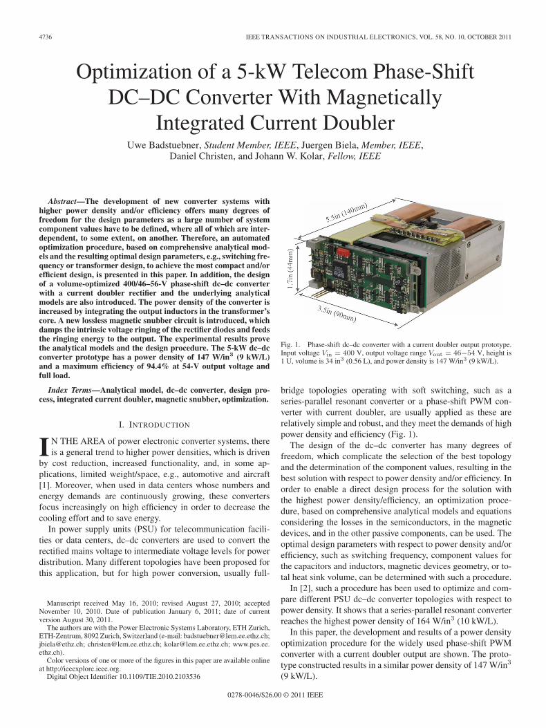
Fig. 1. Phase-shift dc–dc converter with a current doubler output prototype.Input voltage Vin = 400 V, output voltage range Vout = 46−54 V, height is1 U, volume is 34 in3 (0.56 L), and power density is 147 W/in3 (9 kW/L).
bridge topologies operating with soft switching, such as aseries-parallel resonant converter or a phase-shift PWM con-verter with current doubler, are usually applied as these arerelatively simple and robust, and they meet the demands of highpower density and efficiency (Fig. 1).
The design of the dc–dc converter has many degrees offreedom, which complicate the selection of the best topologyand the determination of the component values, resulting in thebest solution with respect to power density and/or efficiency. Inorder to enable a direct design process for the solution withthe highest power density/efficiency, an optimization proce-dure, based on comprehensive analytical models and equationsconsidering the losses in the semiconductors, in the magneticdevices, and in the other passive components, can be used. Theoptimal design parameters with respect to power density and/orefficiency, such as switching frequency, component values forthe capacitors and inductors, magnetic devices geometry, or to-tal heat sink volume, can be determined with such a procedure.
In [2], such a procedure has been used to optimize and com-pare different PSU dc–dc converter topologies with respect topower density. It shows that a series-parallel resonant converterreaches the highest power density of 164 W/in3 (10 kW/L).
In this paper, the development and results of a power densityoptimization procedure for the widely used phase-shift PWMconverter with a current doubler output are shown. The proto-type constructed results in a similar power density of 147 W/in3
(9 kW/L).
0278-0046/$26.00 © 2011 IEEE

BADSTUEBNER et al.: OPTIMIZATION OF A 5-kW TELECOM PHASE-SHIFT DC–DC CONVERTER 4737
Fig. 2. Schematic of the phase-shift full-bridge converter with a currentdoubler rectifier.
The derivation of the analytical models for currents andvoltages, as well as for the design of the magnetic components,is presented in Section II of this paper. The design of thetransformer with integrated output inductors, together withits integrated thermal management, is also discussed in thatsection. The optimization procedure is discussed in Section III.The analytical models applied in the optimization procedure,as well as power density prediction, are validated with themeasurement results on the 5-kW prototype in Section IV.Furthermore, a new lossless snubber circuit for the rectifierdiodes, which could experience high over-voltages in currentdoubler circuits, is presented.
II. PHASE-SHIFT DC–DC CONVERTER WITH
A CURRENT DOUBLER RECTIFIER
The current doubler rectifier is appropriate for telecom ap-plications due to the small output voltage, in contrast to fuelcell power conditioning systems where the usage of a voltagedoubler rectifier could obtain high efficiency [3], [4] and powerdensity.
Alternatively to phase-shift PWM converters, resonanttopologies are suitable in the area of front-end converter sys-tems. In [5], it is shown that a series-parallel resonant converter(LCC) results in a high power density of 164 W/in3 (10 kW/L).Resonant converters have particular advantages concerninghold-up-time requirements, e.g., [6]–[8], part-load efficiencyand secondary side soft-switching ability, as presented for theLCC in [5] and LLC in [6], [9], and [10]; enhanced resonanttopologies, e.g., CLL in [7] and LCLCL in [8]; and secondaryside resonant topologies, as proposed in [11].
Phase-shift PWM converter systems, on the other hand, havethe advantage of commonly smaller circulating energy, smallerrms currents, constant switching frequency, and relative simplecontrol. The full-bridge phase-shift dc–dc converter with acurrent doubler output fulfills the demands with a robust designhaving a high power density and efficiency. As shown in Fig. 2,the converter consists of four switches as part of the full bridge,a transformer which provides galvanic isolation and transformsthe voltage (from 400 to 46–56 V), and a rectifier with twooutput inductors and diodes. As the optimization is focusedon the power density, Schottky diodes with low recovery ef-fects are applied. However, especially in terms of efficiencyoptimization, synchronous rectification should be considered,e.g., as presented in [12]. Moreover, it is possible to reduce
Fig. 3. Switching states and inverter waveforms for the phase-shift converterwith a current doubler, cf., Fig. 1 (φ indicates the phase shift between the twolegs of the full bridge, which determines the duty cycle and, thus, the outputvoltage).
the complexity of the control electronics by applying energy-efficient self-driven synchronous rectifiers, as shown in [13]. Asdemonstrated later in this section, the two output inductors canbe integrated in the transformer in order to reduce the volumeof the magnetic components and to save the space required forinterconnections and mounting. In order to derive the analyticalmodels in Section II-A, the relative simple control scheme andbasic functionalities of the phase-shift converters will be brieflyexplained in this section.
The drawback of this PWM topology is over-voltages oc-curring across the rectifier diodes due to parasitic elementsso that a snubber circuit is recommended in order to applydiodes or switches with lower blocking voltage and, thus, lowerconduction losses. Therefore, a new lossless magnetic snubbercircuit is presented in Section IV-B.
In Fig. 3, the control scheme with the four basic switchingstates and the transformer primary side currents/voltage wave-forms are shown. Each full-bridge switch is turned on for 50%of a switching period. With respect to Fig. 3, the duty cycle Dis adjusted by a phase-shift φ between the control signals of thetwo full-bridge legs (A and B). This leads to four main states:two powering and two freewheeling states.
In the two powering states, the diagonal switches of the legsare switched on (states 1 and 3, cf., Fig. 3), and in the twofreewheeling states, the opposite MOSFETs of the legs areswitched on (states 2 and 4). In powering state 1 (cf., Fig. 3),the primary current iP and the transformer input voltage vP (theinductance Lσ is assumed to be integrated in the transformer)are positive, and so, the rectifier diode D1 conducts the loadand output capacitor current. This current is the sum of the

4738 IEEE TRANSACTIONS ON INDUSTRIAL ELECTRONICS, VOL. 58, NO. 10, OCTOBER 2011
output inductor currents iL1 and iL2 (cf., Fig. 2), which arealmost constant during a switching period. In the next state 2,the positive current iP is freewheeling via MOSFETs s11 ands12, with the current on the secondary side flowing throughboth rectifier diodes. Due to the symmetry of the two legs,switching states 3 and 4 are equal to 1 and 2 with permutedsigns for currents and voltages. A more detailed description ofthe switching states can be found in, for example, [14].
A significant reduction of the switching losses can be ob-tained by zero-voltage switching (ZVS), where the parasiticcapacitances of the MOSFETs in one leg are dis-/chargedduring an interlock delay between the switching states, drivenby the leakage inductance Lσ of the transformer. As shown inSection IV-A, Lσ is enlarged in order to have enough energyfor the recharging process.
A. Analytical Models for the Phase-Shift DC–DC Converter
Analytical models are required for the optimization of thedc–dc converter, which describe the currents/voltages in thecircuit, which model the semiconductor, dielectric, and trans-former losses, and which describe the temperature distributionin the system. The different components can be kept below theirmaximal values in the optimization with the thermal model sothat the components are not destroyed during operation.
These models that follow are based on the phase-shift dc–dcconverter a with current doubler (CDR), as shown in Fig. 2, butare, in particular, also valid for the “integrated” current doubler,as shown in Section II-A4.
1) Analytical Converter Model (cf., Fig. 2): The currentsand voltages, as well as the operating point (phase shift), arecalculated by means of the analytical converter models. Thesevalues are needed to calculate the losses in the semiconductorsand passive components, and thus, the resulting optimizationparameter which is the volume and/or efficiency.
In Fig. 3, the current waveform of the transformer primarycurrent iP is shown. The switched currents of the full-bridgelegs A and B (IP,off,A and IP,off,B), as well as the point wherethe active phase starts (IP,act), are essential for further calcu-lation. In Fig. 3, during the time interval t ∈ [α · TP /2 . . . (1 +α) · TP /2] with a duration of TP /2, iP is positive, and it can bedescribed by the following four piecewise linear parts.
State 1: t ∈ [α · TP /2 . . . (α + β) · TP /2]. The positive inputvoltage vP = +VIN is applied across the transformer, andthe primary current iP increases from zero to IP,act, deter-mined by the transformer leakage inductance Lσ
IP,a =IP,act
β · TP
2
(t − α · TP
2
). (1)
During this interval, both rectifier diodes (D1 and D2) arestill conducting. Thus, the secondary side voltage VS isclamped to zero, and therefore, no power is transferredfrom the primary to the secondary side. At t = (α + β) ·TP /2, the primary current iP is equal to the transformedoutput inductor current iL2 · NS/NP .
State 2: t ∈ [(α + β) · TP /2 . . . D · TP /2]. Delimited by theoutput inductance LS2 and Lσ , the primary current iPincreases from IP,act to IP,off,B . The linearized primarycurrent in powering state 1 can be calculated with
IP,b =IP,off,B−IP,act
(D−(α+β)) · TP
2
·(
t−(α+β) · TP
2
)+IP,act. (2)
At point D · TP /2, iP reaches the maximum value ofIP,max = IP,off,B (cf., Fig. 3), s22 is turned off, and theopposite MOSFET s12 is switched on after a certain inter-lock delay in order to obtain a ZVS condition.
State 3: t ∈ [D · TP /2 . . . TP /2]. During this interval, the pri-mary current is freewheeling (state 2), as shown in Fig. 3.The transformer voltage vP is clamped approximately tozero, and current iP decreases from the turn-off currentof leg B (IP,off,B) down to the turn-off current fromleg A (IP,off,A), determined by Lσ in series with LS1,2 ·(NP /NS)2
IP,c =IP,off,A − IP,off,B
(1 − D) · TP
2
(t − D · TP
2
)+ IP,off,B . (3)
At t = TP /2, the high side switch of leg A (s11) is turnedoff, and diagonal switch s21 is turned on.
State 4: t ∈ [TP /2 . . . (1 + α) · TP /2]. While changing fromfreewheeling state 2 to active state 3, the negative inputvoltage vP = −VIN is applied to the transformer, and iPdecreases to 0 A, determined by Lσ
IP,d =−IP,off,A
α · TP
2
(t − TP
2
)+ IP,off,A. (4)
After that interval, the second half of the switching periodstarts again with the first interval (a) but with a changeddirection of the primary current and voltage.
The rms value of iP (important for the loss calculation) canbe calculated with the current waveform given in (1)–(4)
I2P,rms = 2 · 1
TP
⎡⎢⎢⎣
(α+β)·TP2∫
α·TP2
I2P,adt +
D·TP2∫
(α+β)·TP2
I2P,bdt
+
TP2∫
D·TP2
I2P,cdt +
(1+α)·TP2∫
TP2
I2P,ddt
⎤⎥⎥⎦ .
The duty cycle D, which defines the converter output voltage,is divided into the effective duty cycle De (power transfer),determined by twice of the output voltage VOUT and secondaryside voltage VIN · NS/NP , and a duty cycle loss Dl = (α + β)(cf., Fig. 3) caused by the transformer leakage inductance Lσ
D =2 · VOUT
VIN· NP
NS+ (α + β). (5)
The calculations presented, so far, require the knowledge ofα and β. Furthermore, in addition to the calculation of the rmsvalue in order to calculate the conduction losses, the turn-off

BADSTUEBNER et al.: OPTIMIZATION OF A 5-kW TELECOM PHASE-SHIFT DC–DC CONVERTER 4739
currents IP,off,A,B have to be calculated for the switchinglosses. Additional equations for the continuity of the primarycurrent and output inductor current are needed to solve theseequations for α and β, as shown in [15]. The closed forms for αand β are not included for the sake of brevity. The current wave-forms are defined, and all of the component current/voltagewaveforms can be determined with the obtained values in orderto calculate, for example, the losses in the semiconductors, asdescribed in the next section.
2) Semiconductor Losses: The losses in the power devices(four MOSFETs, including the antiparallel diode and the tworectifier diodes) can be calculated with the results obtained fromthe analytical converter models. The switching losses shown arecalculated based on the empirical equations, determined by themeasurements [5] as a function of the switching frequency fand the turn-off current in leg A and/or B IP,off,A,B
Pzvs,off,A,B = 2 · (1.9 · I2P,off,A,B − 38
· IP,off,A,B + 140) · 10−7 · f (6)
if the turn-off current in leg A and/or B IP,off,A,B ≥ 15 A.When the currents IP,off,A,B are below 15 A, the switchinglosses under the ZVS condition are negligible.
The required heat sink volume is determined based on thecooling system performance index (CSPI) [16], calculatedlosses, maximum permissible junction temperatures, and ther-mal resistance between the junction and the heat sink. It isassumed that, at each point of time, one MOSFET is switchedon, and thus, the current is carried by the MOSFET in theinverse direction (not by the antiparallel diodes). Therefore, theconduction losses of the MOSFETs are calculated with the rmsvalue of the MOSFET current Imos,rms and the MOSFET’s onresistance RDS,on. Due to the ZVS condition, the turn-on lossesare zero, and the turn-off losses in legs A and B are estimatedbased on the measurements for the applied MOSFETs. Forthe rectifier diodes, an approximately constant forward voltagedrop VF,rect is assumed so that the conduction losses Pcond,rect
in one diode can be calculated with the average currents
Pcond,rect = VF,rect · IOUT
2. (7)
As the Schottky diodes are applied, the rectifier switchinglosses are relatively small and are thus neglected.
In order to determine the efficiency, the losses in the gatedrivers and control unit Pgate are also considered. The lossesin the gate drives are dependent on the switching frequency,and they can be calculated with the gate charge, gate–sourcecapacitance, and applied voltage.
3) Output Filter Capacitors: The output filter capacitorscarry high-frequency ripple currents with relatively high am-plitudes. In order to limit the losses and the temperature rise,dielectrics with a low loss factor tan δ are required. In theprototype, 2.2 μF/100 V/X7R ceramic capacitors in a 1210housing from muRata [17], which have a very high allowedripple current per volume ratio, are used.
The voltage over the output capacitor increases during thecharging process, i.e., when the sum of the inductor currents
Fig. 4. Integration of the output inductors of the current doubler in thetransformer core [23].
is greater than the dc-output current (iL > IOUT). This istrue for half of the effective duty cycle De (current increase)and half of the effective freewheeling time (1 − De) (cur-rent decrease). Thus, the capacitance value is calculated withthe currents and the maximum allowed output ripple voltageVripple = 300 mVpp. The losses can be determined with therespective loss factor, and they are compared with the maximumratings from the data sheet. The decrease of the capacitancewith higher temperature and dc voltage is also considered forthe optimization.
4) Transformer Model: In the proposed optimization proce-dure, the shape of the transformer is optimized for minimalvolume while keeping the hot-spot temperatures below thelimits. The losses and the transformer temperature distributionare needed as a function of the geometry for this calculation.
The core losses are calculated by the approach shown in[18], based on the Steinmetz parameters [19] and the rate ofmagnetization (dB/dt). The winding losses are calculated by a1-D approach, which includes the skin and proximity effect loss[20]. Foil windings are used there, allowing a better thermalmanagement. An extended analytical modulation of the coreand winding losses for the nonsinusoidal waveform is shownin [21]. A comparison of the various evaluation approaches canadditionally be found there.
In order to maximize the power density, an advanced coolingmethod has been applied, as described in [5]. The temperaturedistribution resulting from the losses can be calculated withthe thermal model of the transformer. The model describesthe heat flow from the windings/core via thermal interfacesand heat transfer components (HTC) to the heat sinks andambient, respectively. Alternatively, the analytical thermal per-formance modeling of high-energy-density magnetic devices asproposed in [22] could also be implemented in the optimizationalgorithm.
The two output inductors are integrated in the transformerbased on a concept discussed in [23] to decrease the volumeand the losses. In the described dc–dc converter, the conceptshown in Fig. 4 is applied as the flux in the center leg of thetransformer is almost constant, and thus, the core losses aresmall, and standard E-cores could be applied. The value of theintegrated inductors is adapted by the air gap in the center leg.
The operating behavior of the original current doubler alsochanges with the integration shown in Fig. 4. In case of power-ing state 1, i.e., the primary current is positive, a clockwise fluxis induced in the outer legs. Only in the upper secondary wind-ing NS1 (cf., Fig. 4), a current flow is possible, while the current

4740 IEEE TRANSACTIONS ON INDUSTRIAL ELECTRONICS, VOL. 58, NO. 10, OCTOBER 2011
Fig. 5. Automatic procedure in optimizing the volume/efficiency of the phase-shift converter with a current doubler while keeping the device temperaturesbelow the given limits.
flow in the lower winding NS2 is blocked by the diode D2.During freewheeling state 2, the primary current iP remainspositive and allows the current flow still only through diode D1.During states 3 and 4 (cf., Fig. 3), the negative primary currentiP causes the current flow through the secondary winding NS2.This shows a significant change: unlike in the original topologypresented in Fig. 2 where the inductor currents (iL1 and iL2)are almost constant over a switching period, the current inthe integrated topology flows only over one of the secondarywinding/inductor. Thus, the original name “current doubler” is,in principle, not entirely correct any more. However, the currentand voltage waveforms outside of the integrated transformerremain the same as with the original current doubler, as shownin Fig. 2, and the described models are still valid.
The optimization results presented in Section IV are based onthe net volume of the magnetic devices. It has been shown thatthe net volume of the integrated and original current doubler isalmost even. Nevertheless, the power density of the system canbe increased with the integrated current doubler as less spacefor connections, terminals, and spacing is required.
III. POWER DENSITY OPTIMIZATION PROCEDURE
Based on the analytical models presented in the previous sec-tion, an automatic optimization procedure has been developedin finding the best set of design parameters which result in amaximal power density and/or efficiency. This comprehensivedesign approach, which yields in the best converter systemperformance with respect to the optimization constraints andspecification, has been proved in several power electronic areas,as shown, for example, in [24]. In the proposed procedure
TABLE ISPECIFICATIONS FOR THE PROTOTYPE IT DC–DC CONVERTER
shown in Fig. 5, all fixed electrical, thermal, and magnetic com-ponent parameters and specifications are preset in the first step.These are (besides the system specifications, e.g., input/outputvoltage VIN/VOUT, output power POUT, and ambient temper-ature Tamb) the characteristics of the employed components,like the thermal resistances of the semiconductors, isolationmaterials, and thermal grease, and the characteristics of the corematerials.
It is possible to include the material and device specificationsas design parameters in the optimization algorithm, e.g., with adatabase. The programming effort is relatively small, but theimplementation would result in a drastically increased compu-tation time. The proposed procedure requires preselecting theoptimal device based on the pre-runs of the respective part ofthe optimization procedure in order to keep the computationtime low.
In the next step, the design parameters, such as the switch-ing frequency, the number of windings, and the permissiblecurrent ripple, are set as the initial values for the calculation.The operating point is calculated with the defined constraintsand parameter settings and with the equations presented inSection II-A. This is characterized, for instance, by the dutycycle D, the duty cycle loss α + β, the primary current wave-form characteristic IP,off,A,B/IP,1, and the output inductancesLS1,2. The transformer and the inductor are optimized with thecalculated operating point with respect to the power densityand/or efficiency within an inner optimization procedure whilekeeping the temperatures for the core and windings belowthe maximum values. Furthermore, the volume of the filtercapacitors can be directly calculated, and the heat sinks can bedetermined by the losses in combination with the CSPI [16].The global optimization procedure systematically changes thedesign parameters in minimizing the overall system volumeand/or efficiency.
IV. OPTIMIZATION, CONSTRUCTION,AND MEASUREMENT RESULTS
The phase-shift converter with a current doubler has beenoptimized for the given specifications in Table I by use ofthe optimization procedure presented in Section III. Amongothers, the following components/limitations have been usedfor calculation:
1) core material N87 from Epcos (Tmax ≤ 115 ◦C);2) foil windings (Tmax ≤ 125 ◦C);3) microsemi MOSFET APT50M75;4) microsemi diodes APT100S20;5) maximal junction temperature Tj,max ≤ 140 ◦C.
BADSTUEBNER et al.: OPTIMIZATION OF A 5-kW TELECOM PHASE-SHIFT DC–DC CONVERTER 4741
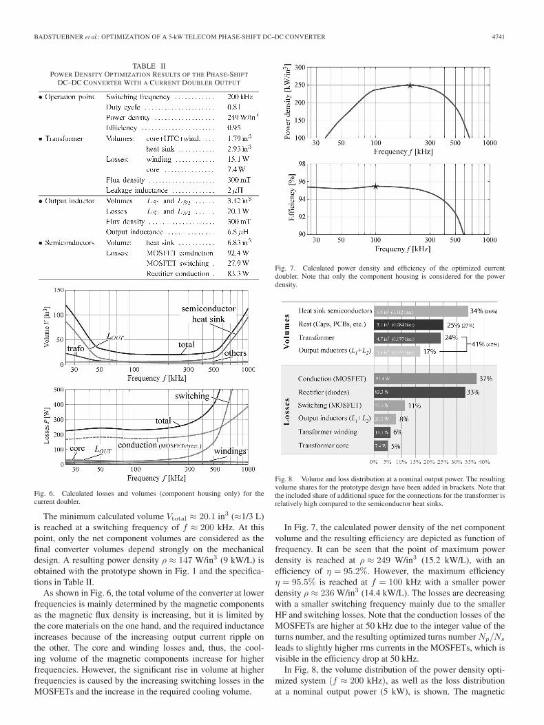
TABLE IIPOWER DENSITY OPTIMIZATION RESULTS OF THE PHASE-SHIFT
DC–DC CONVERTER WITH A CURRENT DOUBLER OUTPUT
Fig. 6. Calculated losses and volumes (component housing only) for thecurrent doubler.
The minimum calculated volume Vtotal ≈ 20.1 in3 (≈1/3 L)is reached at a switching frequency of f ≈ 200 kHz. At thispoint, only the net component volumes are considered as thefinal converter volumes depend strongly on the mechanicaldesign. A resulting power density ρ ≈ 147 W/in3 (9 kW/L) isobtained with the prototype shown in Fig. 1 and the specifica-tions in Table II.
As shown in Fig. 6, the total volume of the converter at lowerfrequencies is mainly determined by the magnetic componentsas the magnetic flux density is increasing, but it is limited bythe core materials on the one hand, and the required inductanceincreases because of the increasing output current ripple onthe other. The core and winding losses and, thus, the cool-ing volume of the magnetic components increase for higherfrequencies. However, the significant rise in volume at higherfrequencies is caused by the increasing switching losses in theMOSFETs and the increase in the required cooling volume.
Fig. 7. Calculated power density and efficiency of the optimized currentdoubler. Note that only the component housing is considered for the powerdensity.
Fig. 8. Volume and loss distribution at a nominal output power. The resultingvolume shares for the prototype design have been added in brackets. Note thatthe included share of additional space for the connections for the transformer isrelatively high compared to the semiconductor heat sinks.
In Fig. 7, the calculated power density of the net componentvolume and the resulting efficiency are depicted as function offrequency. It can be seen that the point of maximum powerdensity is reached at ρ ≈ 249 W/in3 (15.2 kW/L), with anefficiency of η = 95.2%. However, the maximum efficiencyη = 95.5% is reached at f = 100 kHz with a smaller powerdensity ρ ≈ 236 W/in3 (14.4 kW/L). The losses are decreasingwith a smaller switching frequency mainly due to the smallerHF and switching losses. Note that the conduction losses of theMOSFETs are higher at 50 kHz due to the integer value of theturns number, and the resulting optimized turns number Np/Ns
leads to slightly higher rms currents in the MOSFETs, which isvisible in the efficiency drop at 50 kHz.
In Fig. 8, the volume distribution of the power density opti-mized system (f ≈ 200 kHz), as well as the loss distributionat a nominal output power (5 kW), is shown. The magnetic
4742 IEEE TRANSACTIONS ON INDUSTRIAL ELECTRONICS, VOL. 58, NO. 10, OCTOBER 2011
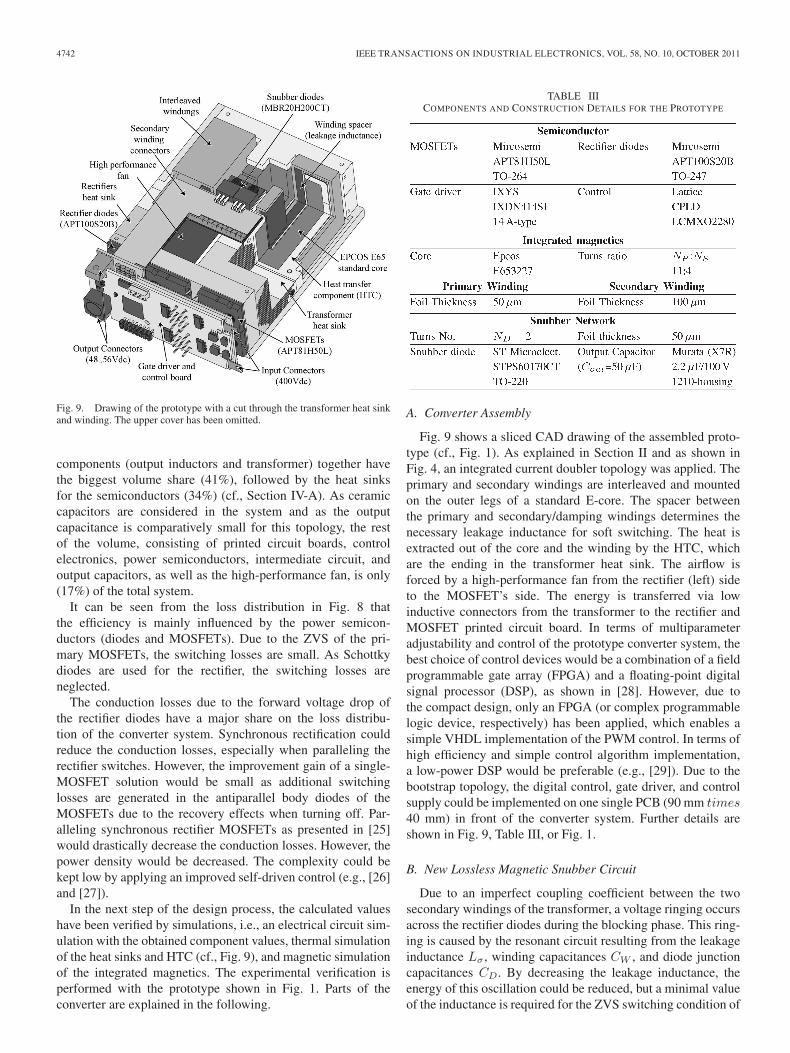
Fig. 9. Drawing of the prototype with a cut through the transformer heat sinkand winding. The upper cover has been omitted.
components (output inductors and transformer) together havethe biggest volume share (41%), followed by the heat sinksfor the semiconductors (34%) (cf., Section IV-A). As ceramiccapacitors are considered in the system and as the outputcapacitance is comparatively small for this topology, the restof the volume, consisting of printed circuit boards, controlelectronics, power semiconductors, intermediate circuit, andoutput capacitors, as well as the high-performance fan, is only(17%) of the total system.
It can be seen from the loss distribution in Fig. 8 thatthe efficiency is mainly influenced by the power semicon-ductors (diodes and MOSFETs). Due to the ZVS of the pri-mary MOSFETs, the switching losses are small. As Schottkydiodes are used for the rectifier, the switching losses areneglected.
The conduction losses due to the forward voltage drop ofthe rectifier diodes have a major share on the loss distribu-tion of the converter system. Synchronous rectification couldreduce the conduction losses, especially when paralleling therectifier switches. However, the improvement gain of a single-MOSFET solution would be small as additional switchinglosses are generated in the antiparallel body diodes of theMOSFETs due to the recovery effects when turning off. Par-alleling synchronous rectifier MOSFETs as presented in [25]would drastically decrease the conduction losses. However, thepower density would be decreased. The complexity could bekept low by applying an improved self-driven control (e.g., [26]and [27]).
In the next step of the design process, the calculated valueshave been verified by simulations, i.e., an electrical circuit sim-ulation with the obtained component values, thermal simulationof the heat sinks and HTC (cf., Fig. 9), and magnetic simulationof the integrated magnetics. The experimental verification isperformed with the prototype shown in Fig. 1. Parts of theconverter are explained in the following.
TABLE IIICOMPONENTS AND CONSTRUCTION DETAILS FOR THE PROTOTYPE
A. Converter Assembly
Fig. 9 shows a sliced CAD drawing of the assembled proto-type (cf., Fig. 1). As explained in Section II and as shown inFig. 4, an integrated current doubler topology was applied. Theprimary and secondary windings are interleaved and mountedon the outer legs of a standard E-core. The spacer betweenthe primary and secondary/damping windings determines thenecessary leakage inductance for soft switching. The heat isextracted out of the core and the winding by the HTC, whichare the ending in the transformer heat sink. The airflow isforced by a high-performance fan from the rectifier (left) sideto the MOSFET’s side. The energy is transferred via lowinductive connectors from the transformer to the rectifier andMOSFET printed circuit board. In terms of multiparameteradjustability and control of the prototype converter system, thebest choice of control devices would be a combination of a fieldprogrammable gate array (FPGA) and a floating-point digitalsignal processor (DSP), as shown in [28]. However, due tothe compact design, only an FPGA (or complex programmablelogic device, respectively) has been applied, which enables asimple VHDL implementation of the PWM control. In terms ofhigh efficiency and simple control algorithm implementation,a low-power DSP would be preferable (e.g., [29]). Due to thebootstrap topology, the digital control, gate driver, and controlsupply could be implemented on one single PCB (90 mm times40 mm) in front of the converter system. Further details areshown in Fig. 9, Table III, or Fig. 1.
B. New Lossless Magnetic Snubber Circuit
Due to an imperfect coupling coefficient between the twosecondary windings of the transformer, a voltage ringing occursacross the rectifier diodes during the blocking phase. This ring-ing is caused by the resonant circuit resulting from the leakageinductance Lσ , winding capacitances CW , and diode junctioncapacitances CD. By decreasing the leakage inductance, theenergy of this oscillation could be reduced, but a minimal valueof the inductance is required for the ZVS switching condition of

BADSTUEBNER et al.: OPTIMIZATION OF A 5-kW TELECOM PHASE-SHIFT DC–DC CONVERTER 4743
Fig. 10. (a) Schematic of the proposed “lossless” magnetic snubber circuitfor the integrated current doubler rectifier diode. The snubber circuit for onlyone diode is drawn for simplicity. (b) Measurement results of the rectifier diodevoltage VD1. In order not to destroy the rectifier diodes by over-voltage, themeasurements are performed at an input voltage VIN = 200 V, 1 kW, andVOUT ≈ 35 V.
the MOSFETs. This effect is even enhanced for the integratedtopology because of the current shift from the first secondarywinding (NS1) to the other (NS2). Furthermore, in reducingthe magnetic component volume, the switching frequency willbe increased, and the winding capacitance is relatively highsince, in the prototype, system foil windings are utilized. Inorder to decrease the occurring ringing without decreasing theefficiency, a lossless snubber circuit for the diodes is required.In [30], several electrical lossless snubber circuits have beenpresented, which transfer a large share of the ringing energy tothe output. However, the first voltage peak could not be damped.
In Fig. 10(a), a new circuit, which requires only a singlesnubber diode DS1 and an additional small winding ND, ispresented. The idea behind this topology is transferring theleakage energy directly with the damping winding to the output.In principle, the damping winding could also be installed onthe center leg of the core. However, the coupling between thesecondary windings NS1,2 would be lower. The voltage over thesecondary winding during the blocking phase is transformedwith the turns ratio ND : NS1,2 to the snubber diode voltageVDS1,2 and is clamped over the output voltage. The maximumdiode voltages VD1,2,max can be set with the damping winding’snumber of turns ND
ND = NS · VOUT
VD1,2,max − VOUT. (8)
The snubber diodes DS1 start conducting as soon as VD1 >VD1,max, and the oscillation energy is directly fed to the output,with a proper choice of VD1,2,max slightly over the steady-statevoltage of VD1,2 .
The maximum steady-state blocking voltage VDS ,max acrossthe snubber diodes DS1,2 is VDS ,max = VOUT · (1 + ND/NS).For an output voltage of VOUT = 50 V and with the designparameters given in Table III, the maximum blocking voltage isVDS ,max = 75 V, which enables applying the Schottky diodes.
In Fig. 10(b), the measurement results of the rectifier diodevoltage VD1 are presented. Compared to the original curves[gray and marked “undamped” in Fig. 10(b)], the proposedsnubber circuit significantly reduces the ringing: the amplitudeis damped by a factor of four. In particular, the first peak issignificantly reduced in comparison to other lossless snubbers.
Fig. 11. Measured curves: primary voltage vP , primary current iP , andrectifier diode voltage vD1 at 5-kW output power.
Fig. 12. Measurement results: efficiency as a function of the output power fordifferent output voltages.
C. Measurement Results
The thermal and electrical measurements have been per-formed with the prototype presented for the validation of thecalculation and simulation results. The results are shown forthe interleg voltage vP , primary current iP , and rectifier voltagevD1 in Fig. 11. Due to the ZVS, vP shows no voltage ringing atfull power, and the rectifier diode voltage ringing is drasticallydecreased by the lossless snubber circuit. Only a small amountof avalanche energy is produced within the diodes because ofthe present small voltage overshoot directly after the commuta-tion. This justifies the application of the selected rectifier diodesoperating in the specified SOA. Without a damping network,voltage ringing would be much higher, forcing the selection ofdiodes with a higher blocking voltage ability, and the Schottkydiodes are possibly not available for the required voltage.Alternative applied silicon diodes would cause additional lossesdue to recovery effects, which would lead to a higher volumefor the heat sinks.
The primary current waveform in Fig. 11 immediately afterthe input voltage is applied to the transformer differs from theideal waveform in Fig. 3. The observed current peak occurs dueto the active damping network, which takes part at the powerconversion in this phase. As soon as the damping network getsinactive after a certain time, the current slope is similar to thetheoretical current doubler waveforms without oscillations.
In Fig. 12, the measured efficiency at part load and fordifferent output voltage levels is shown. As shown in Fig. 8,the efficiency is mainly influenced by the conduction losses of

4744 IEEE TRANSACTIONS ON INDUSTRIAL ELECTRONICS, VOL. 58, NO. 10, OCTOBER 2011
Fig. 13. Measurement results: infrared picture at POUT = 5.1 kW andVOUT = 54 V. Note that the ambient temperature was 20 ◦C, unlike theassumed 40 ◦C for the calculation.
the power semiconductors, which explains the higher efficiencylevels for higher output voltages because of the smaller currentrms values. The efficiency curves are flat in the load range20%–100%, and the calculated efficiency (95.2%) is validatedby the measured efficiency (94.4%) at nominal power. Notethat, in the optimization procedure presented, only the fullload is considered for the power density, and the converteris designed to be operated in the middle load range up tofull load. A higher part-load efficiency can be achieved byapplying enhanced topologies (e.g., [31]). In addition, in [29],an enhanced efficiency optimization algorithm is presented,which also considers the part-load efficiency.
Furthermore, the thermal design could be validated by theinfrared temperature measurements. As shown in Fig. 13, theheat sink temperature of the MOSFET is 94 ◦C (100 ◦C calcu-lated), and that of the rectifier is 113 ◦C (112 ◦C calculated).(Note that the ambient temperature in Fig. 13 was 20 ◦C andnot 40 ◦C like in the calculation. Thus, 20 ◦C has been addedto the measured temperature for comparison.) However, thehot-spot temperature can be found on the rectifier terminals.The entire current is flowing through one anode terminal ofthe used Schottky rectifier diode. Due to the eddy currentand crowding effects and, particularly, the terminal connectionresistance, more than 30 W of additional losses occurs in theterminals, which leads to a reduced efficiency in comparison tothe calculated one.
V. CONCLUSION
In this paper, a 400/46–56-V 5-kW telecom phase-shiftdc–dc converter with an integrated current doubler rectifier hasbeen analytically described, including the models for semicon-ductor losses, transformer HF winding and core losses, andvolumes, as well as for thermal management. Based on thesecomprehensive models, an optimization procedure with respectto power density is applied to determine the component values.After verifying the resulting parameters by electrical, thermal,and magnetic simulations, a prototype has been constructed,which has a power density of 147 W/in3 (9 kW/L) and amaximum efficiency of 94.4% and which integrates the outputinductors in the transformer. The prototype measurements val-idate the analytical calculations. Furthermore, a new snubber
circuit for the rectifier diodes, which performs an almost loss-less damping of the diode voltage, is presented and validated bythe measurements.
The power density barrier for this topology is identified withthe presented approach. The comparison with the optimizedseries-parallel resonant converter in [5] shows that the opti-mized maximum power density of a converter system is almosttopology independent in these two cases. The advancement ofa single component leads only to small improvements of theoptimal point. A higher efficiency can only be obtained withthe reduction of the power density.
REFERENCES
[1] J. W. Kolar, U. Drofenik, J. Biela, M. L. Heldwein, H. Ertl, T. Friedli, andS. D. Round, “PWM converter power density barriers,” in Proc. 4th PCC,Apr. 2007, pp. 9–29.
[2] J. Biela, U. Badstuebner, and J. W. Kolar, “Impact of power densitymaximization on efficiency of dc–dc converter systems,” IEEE Trans.Power Electron., vol. 24, no. 1, pp. 288–300, Jan. 2009.
[3] J. M. Kwon, E. H. Kim, B. H. Kwon, and K. H. Nam, “High-efficiencyfuel cell power conditioning system with input current ripple reduction,”IEEE Trans. Ind. Electron., vol. 56, no. 3, pp. 826–834, Mar. 2009.
[4] M. Nymand and M. A. E. Andersen, “High-efficiency isolated boost dc–dcconverter for high-power low-voltage fuel-cell applications,” IEEE Trans.Ind. Electron., vol. 57, no. 2, pp. 505–514, Feb. 2010.
[5] J. Biela, U. Badstuebner, and J. W. Kolar, “Design of a 5-kW, 1-U,10-kW/dm3 resonant dc–dc converter for telecom applications,” IEEETrans. Power Electron., vol. 24, no. 7, pp. 1701–1710, Jul. 2009.
[6] D. Fu, B. Lu, and F. C. Lee, “1 MHz high efficiency LLC resonantconverters with synchronous rectifier,” in Proc. IEEE Power Electron.Spec. Conf., Jun. 2007, pp. 2404–2410.
[7] D. Huang, D. Fu, and F. C. Lee, “High switching frequency, high effi-ciency CLL resonant converter with synchronous rectifier,” in Proc. IEEEECCE, Sep. 2009, pp. 804–809.
[8] D. Fu, F. C. Lee, Y. Liu, and M. Xu, “Novel multi-element resonantconverters for front-end dc/dc converters,” in Proc. IEEE Power Electron.Spec. Conf., Jun. 2008, pp. 250–256.
[9] J. A. Sabate, M. M. Jovanovic, F. C. Lee, and R. T. Gean, “Analysisand design-optimization of LCC resonant inverter for high-frequency acdistributed power system,” IEEE Trans. Ind. Electron., vol. 42, no. 1,pp. 63–71, Aug. 1995.
[10] B. Yang, F. Lee, A. Zhang, and G. Huang, “LLC resonant converter forfront end dc/dc conversion,” in Proc. 17th Annu. IEEE APEC, Mar. 2002,vol. 2, pp. 1108–1112.
[11] E. H. Kim and B. H. Kwon, “Zero-voltage- and zero-current-switchingfull-bridge converter with secondary resonance,” IEEE Trans. Ind.Electron., vol. 57, no. 3, pp. 1017–1025, Feb. 2010.
[12] H. J. Chiu and L. W. Lin, “A high-efficiency soft-switched ac/dc con-verter with current-doubler synchronous rectification,” IEEE Trans. Ind.Electron., vol. 52, no. 3, pp. 709–718, May 2005.
[13] A. Fernandez, D. G. Lamar, M. Rodriguez, M. M. Hernando, andJ. S. M. Arias, “Self-driven synchronous rectification system with inputvoltage tracking for converters with a symmetrically driven transformer,”IEEE Trans. Ind. Electron., vol. 56, no. 5, pp. 1440–1445, May 2009.
[14] B. R. Lin, K. Huang, and D. Wang, “Analysis and implementation offull-bridge converter with current doubler rectifier,” Proc. Inst. Elect.Eng.—Elect. Power Appl., vol. 152, no. 5, pp. 1193–1202, Sep. 2005.
[15] U. Badstuebner, J. Biela, B. Faessler, D. Hoesli, and J. W. Kolar, “An op-timized 5 kW, 147 W/in3 telecom phase-shift dc–dc converter with mag-netically integrated current doubler,” in Proc. 24th Annu. IEEE APEC,Mar. 2009, vol. 24, pp. 21–27.
[16] U. Drofenik, G. Laimer, and J. W. Kolar, “Theoretical converter powerdensity limits for forced convection cooling,” in Proc. Int. Conf.Power Electron., Intell. Motion Power Quality (PCIM Eur.), Jun. 2005,pp. 608–619.
[17] Homepage of muRata Manufacturing Co., Ltd. [Online]. Available:http://www.murata.com/
[18] K. Venkatachalam, C. R. Sullivan, T. Abdallah, and H. Tacca, “Accu-rate prediction of ferrite core loss with nonsinusoidal waveforms usingonly Steinmetz parameters,” in Proc. IEEE Workshop Comput. PowerElectron., Jun. 2002, pp. 36–41.

BADSTUEBNER et al.: OPTIMIZATION OF A 5-kW TELECOM PHASE-SHIFT DC–DC CONVERTER 4745
[19] C. P. Steinmetz, “On the law of hysteresis,” Proc. IEEE, vol. 72, no. 2,pp. 197–221, Feb. 1984.
[20] W. G. Hurley, E. Gath, and J. G. Breslin, “Optimizing the ac resistance ofmultilayer transformer windings with arbitrary current waveforms,” IEEETrans. Power Electron., vol. 15, no. 2, pp. 369–376, Mar. 2000.
[21] I. Villar, U. Viscarret, I. Etxeberria-Otadui, and A. Rufer, “Global lossevaluation methods for nonsinusoidally fed medium-frequency powertransformers,” IEEE Trans. Ind. Electron., vol. 56, no. 10, pp. 4132–4140,Oct. 2009.
[22] R. Wrobel, N. McNeill, and P. H. Mellor, “Performance analysis andthermal modeling of a high-energy-density prebiased inductor,” IEEETrans. Ind. Electron., vol. 57, no. 1, pp. 201–208, Jan. 2010.
[23] P. Xu, Q. Wu, P.-L. Wong, and F. C. Lee, “A novel integrated currentdoubler rectifier,” in Proc. 15th Annu. IEEE APEC, Feb. 2000, vol. 2,pp. 735–740.
[24] T. Nussbaumer, K. Raggl, and J. W. Kolar, “Design guidelines for in-terleaved single-phase boost PFC circuits,” IEEE Trans. Ind. Electron.,vol. 56, no. 7, pp. 2559–2573, Jul. 2009.
[25] U. Badstuebner, J. Biela, and J. W. Kolar, “An optimized, 99% efficient,5 kW, phase-shift PWM dc–dc converter for data centers and telecomapplication,” in Proc. IPEC, Jun. 2010, pp. 626–634.
[26] X. Xie, J. C. P. Liu, F. N. K. Poon, and M. H. Pong, “A novel highfrequency current-driven synchronous rectifier for low voltage high cur-rent applications,” in Proc. 16th Annu. IEEE APEC, Mar. 2001, vol. 1,pp. 469–475.
[27] D. Fu, Y. Liu, F. C. Lee, and M. Xu, “A novel driving scheme for synchro-nous rectifiers in LLC resonant converters,” IEEE Trans. Power Electron.,vol. 24, no. 5, pp. 1321–1329, May 2009.
[28] E. J. Bueno, A. Hernandez, F. J. Rodriguez, C. Giron, R. Mateos, andS. Cobreces, “A DSP- and FPGA-based industrial control with high-speedcommunication interfaces for grid converters applied to distributed powergeneration systems,” IEEE Trans. Ind. Electron., vol. 56, no. 3, pp. 654–669, Mar. 2009.
[29] U. Badstuebner, J. Biela, and J. Kolar, “Design of an 99%-efficient, 5 kW,phase-shift PWM dc–dc converter for telecom applications,” in Proc. 25thAnnu. IEEE APEC, Feb. 2010, pp. 773–780.
[30] H. Mao, J. A. Abu-Qahouq, W. Qiu, Y. Wen, and I. Batarseh, “Losslesssnubber circuits for current doubler rectifiers to reduce reverse-recoverylosses,” in Proc. 29th IEEE IECON, Nov. 2003, vol. 3, pp. 2639–2644.
[31] S. S. Lee and G. W. Moon, “Full ZVS-range transient current buildup half-bridge converter with different ZVS operations to load variation,” IEEETrans. Ind. Electron., vol. 55, no. 6, pp. 2557–2559, Jun. 2008.
Uwe Badstuebner (S’07) received the Dipl.Ing. de-gree (with honors) from the Technical Universityof Berlin, Berlin, Germany, in 2006. He is cur-rently working toward the Ph.D. degree in the PowerElectronic Systems Laboratory, Swiss Federal Insti-tute of Technology Zurich (ETH Zurich), Zurich,Switzerland. He studied electrical engineering atthe University of Technology, Berlin, Germany, ma-joring in measurement technology and automaticcontrol systems. He additionally studied power elec-tronics and electronics.
He was engaged in research at the Departments of Research and Technologyof Osram and DaimlerChrysler. His research is focused on power density andefficiency optimization, and modeling and design of converter systems.
Juergen Biela (S’04–M’06) received the Diploma(with honors) in electrical engineering from theFriedrich-Alexander University, Erlangen, Germany,in 2000 and the Ph.D. degree in electrical engineer-ing from ETH Zurich, Zurich, Switzerland, in 2005.
While taking his M.S. degree, he also studiedat the University of Strathclyde, Glasgow, U.K.,and at the Technical University of Munich, Munich,Germany. From 2000 to 2002, he worked at the Re-search Department, A&D Siemens. In July 2002, hewas with the Power Electronic Systems Laboratory
(PES), ETH Zurich, while working toward his Ph.D. degree. After finishing hisPh.D. degree in 2005, he worked as a Postdoctoral Fellow (2006–2007) andas a Senior Scientist (2008–2010) at PES. In 2007, he was a Guest Researcherwith the Tokyo Institute of Technology, Tokyo, Japan. He has been an AssociateProfessor of high-power electronics with the ETH Zurich since August 2010.
Daniel Christen studied electrical engineering at theETH Zurich, Zurich, Switzerland, where he dealtwith power electronics and control engineering.
In his master’s thesis, he designed and improveda dc–dc converter with a current doubler outputstage. Since January 2009, he has been a ResearchAssistant with the ETH Zurich. His current researchis focused on calorimetric power measurement.
Johann W. Kolar (M’89–SM’04–F’10) receivedthe M.Sc. and Ph.D. degrees (summa cum laude/promotio sub auspiciis praesidentis rei publicae)from the University of Technology Vienna, Vienna,Austria.
Since 1984, he has been working as an Indepen-dent International Consultant in close collaborationwith the University of Technology Vienna in thefields of power electronics, industrial electronics, andhigh-performance drives. He has proposed numerousnovel PWM converter topologies and modulation
and control concepts, e.g., the VIENNA rectifier and the three-phase ac–acsparse matrix converter. He was appointed as a Professor and the Head of thePower Electronic Systems Laboratory, Swiss Federal Institute of TechnologyZurich (ETH Zurich), Zurich, Switzerland, on February 1, 2001. He haspublished over 350 scientific papers in international journals and conferenceproceedings and has filed more than 75 patents. The focus of his currentresearch is on ac–ac and ac–dc converter topologies with low effects onthe mains, e.g., for power supply of data centers, more electric aircraft, anddistributed renewable energy systems. Further main areas of research are therealization of ultracompact and ultraefficient converter modules employing thelatest power semiconductor technology (SiC and GaN), novel concepts forcooling and EMI filtering, multidomain/scale modeling/simulation and multi-objective optimization, physical model-based lifetime prediction, pulsed power,and ultrahigh speed and bearingless motors. In 2006, the European PowerSupplies Manufacturers Association (EPSMA) awarded the Power ElectronicsSystems Laboratory, ETH Zurich, as the leading academic research institutionin power electronics in Europe.