OPTIMAL FILTER DESIGN AND SWITCHING LOSS REDUCTION IN...
50
OPTIMAL FILTER DESIGN AND SWITCHING LOSS REDUCTION IN SINGLE PHASE GRID CONNECTED INVERTER SYSTEM TONTEPU NAGA SOWMYA (109EE0052) DEBATI MARANDI (109EE0280) Department of Electrical Engineering National Institute of Technology Rourkela
Transcript of OPTIMAL FILTER DESIGN AND SWITCHING LOSS REDUCTION IN...
OPTIMAL FILTER DESIGN AND SWITCHING LOSS
REDUCTION IN SINGLE PHASE GRID CONNECTED
INVERTER SYSTEM
TONTEPU NAGA SOWMYA (109EE0052)
DEBATI MARANDI (109EE0280)
Department of Electrical Engineering National Institute of Technology Rourkela
ii
OPTIMAL FILTER DESIGN AND SWITCHING LOSS
REDUCTION IN SINGLE PHASE GRID CONNECTED
INVERTER SYSTEM
A Thesis submitted in partial fulfillment of the requirements for the degree of
Bachelor of Technology in “Electrical Engineering”
By
TONTEPU NAGA SOWMYA (109EE0052)
DEBATI MARANDI (109EE0280)
Under guidance of
Prof. B.CHITTI BABU
Department of Electrical Engineering National Institute of Technology
Rourkela-769008 (ODISHA) May-2013

This is to
in single
No.109E
requirem
2012-201
carried o
The cand
The thes
degree/di
In my op
in Electri
o certify tha
e phase grid
EE0052) and
ments for the
13 at Nation
ut by them u
didates have
sis which is
iploma.
pinion, the th
ical Enginee
C
at the thesis
d connected
d Debati M
award of B
nal Institute
under my sup
fulfilled all
s based on
hesis is of st
ering.
D
NATIONA
ERT
entitled “Op
inverter sy
Marandi (R
Bachelor of T
of Technolo
pervision an
the prescrib
candidates’
tandard requ
iii
DEPARTME
AL INSTITU
TIFIC
ptimal Filte
ystem”, subm
Roll No. 10
Technology in
ogy, Rourke
nd guidance.
ed requirem
’ own work
uired for the
ENT OF ELE
UTE OF TEC
CATE
er design an
mitted by To
09EE0280)
n Electrical
ela. A bonaf
ments.
k, have not
award of a
Dep Natio
ECTRICAL
CHNOLOGY
ODISHA
E
nd Switchin
ontepu Nag
in partial f
l Engineerin
fide record o
submitted
bachelor of t
D
pt. of Electrional institut
R
ENGINEER
Y, ROURKE
, INDIA-76
ng loss redu
ga Sowmya
fulfilment o
ng during se
of research
elsewhere
technology de
Dr. B.ChittiBSuper
ical Engineete of TechnoRourkela-76
RING
ELA
69008
ction
(Roll
f the
ession
work
for a
egree
Babu visor ering ology 69008

iv
ACKNOWLEDGEMENTS
This project is done as our final year project, as a part of course .We are really thankful to our
project guide Prof. B Chitti Babu, Assistant Professor, Department of Electrical Engineering, for
his invaluable guidance and assistance, without which the accomplishment of the task would have
never been possible. He inspired us greatly to work in this project. His willingness to motivate us
contributed tremendously to our project. We also would like to thank him for showing us some
example that related to the topic of our project. We would also thank our friends who helped
during our project.
Tontepu Naga Sowmya
Debati Marandi
B.Tech (Electrical Engineering)

v
Dedicated to Our lovable parents and Friends...

vi
ABSTRACT
With the reduction of available fossil fuels, the research in the area of renewable energy
system has been exponentially increased in order to find out an effective solution. Considering the
case of a PV panel, it is observed that it produces a DC voltage which has to be converted to AC
for grid connected applications. So a Voltage Source Inverter (VSI) with a PWM control of
switching action is used for this purpose.
This project presents the comparative study between unipolar and bi-polar switching
scheme for single–phase grid-connected inverter system with filter design on the grid side. For
that, LCL filter is considered and its performance for current ripple reduction on grid-side is
compared with normal L and LC filter. It is seen that the response for LCL filter show the best
results with lower current ripple as compared to L and LC Filter. Further, the obtained results
show that the obtained LCL-filter can provide sufficient attenuation of current harmonics and
mean while injects a sinusoidal current into the grid for maintaining power quality standard. In
addition to that, the method to design the inductor is also studied.
Further, the optimal design of LCL filter for grid connected inverter system is studied. For
that, initially normal design is considered. Then the conduction and switching losses that are
caused by the filter are calculated and are optimized considering the level of reduction of
harmonics. Hence the main aim of the study is to attenuate higher order harmonics along with the
reduction in switching losses to ensure sinusoidal current injection into the grid. Further, the
different switching schemes for single phase unipolar full bridge inverter are studied and
compared to get the switching scheme which gives lesser switching losses. The LCL filter is
designed accordingly and optimal inductance and capacitance values are obtained. The complete
model of the study is simulated in MATLAB-Simulink environment for feasibility of the study.
vii
CONTENTS
Abstract v
Contents vii
List of Figures ix
List of Tables x
Abbreviations and Acronyms xi
CHAPTER 1
INTRODUCTION
1.1 Motivation 2
1.2 Introduction 2
1.3 Literature review 4
1.4 Organization of thesis 4
CHAPTER 2 MATHEMATICAL MODELLING OF SINGLE PHASE VOLTAGE SOURCE
INVERTER
2.1 Mathematical modeling of an inverter 2.1.1 Unipolar Switching Control 7
2.1.2 Bipolar Switching Control 11
CHAPTER 3 LCL FILTER DESIGN
3.1 Types of filter 14
3.2 LCL filter with passive damping 14
3.3 Optimal LCL filter design 15

viii
CHAPTER 4 SWITCHING LOSS REDUCTION WITH LCL FILTER
4.1 Different switching methods 20
4.2 Reduction of switching losses 21
CHAPTER 5
SIMULATION RESULTS AND DISCUSSIONS 23
CHAPTER 6 CONCLUSION AND FUTURE WORK
6.1 Conclusion 30
6.2 Future Work 30
References 31
Appendix
a) Small signal analysis of single phase inverter 34
b) Inductor design of the filter 37
Publication(s) 39

ix
LIST OF FIGURES
Fig.1.1. Single phase grid connected inverter with LCL filter. (3)
Fig.2.1. Shows the topology for single phase full bridge inverter (7)
Fig.2.2.Output voltage and current waveform of unipolar switching scheme inverters (8)
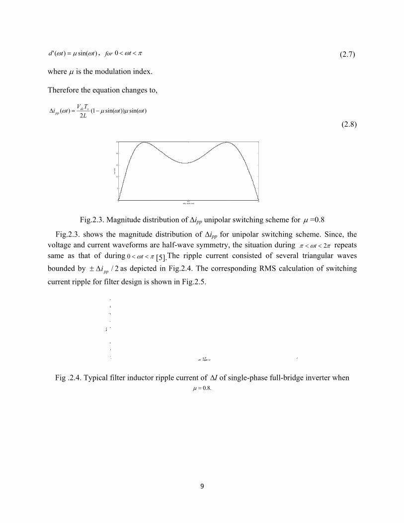
Fig.2.3. Magnitude distribution of ∆ipp unipolar switching scheme for μ =0.8 (9)
Fig .2.4. Typical filter inductor ripple current of IΔ of single-phase full-bridge inverter when .8.0=μ (9)
Fig .2.5. RMS calculation of the equivalent of filter inductor ripple current ∆i (10)
Fig.2.6. Output voltage and current waveform of bipolar switching scheme inverters (11)
Fig.2.7.Magnitude distribution of ∆ipp bipolar switching scheme for μ =0.8 (11)
Fig.2.8 Response of typical filter inductor ripple current of IΔ of single-phase half-bridge inverter when (12) Fig.3.1.LCL filter design with passive damping (16)
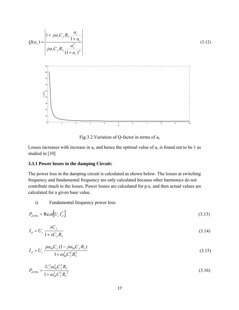
Fig.3.2.Variation of Q-factor in terms of ac (17)
Fig.5.1 Variation of total power losses with L in p.u (25)
Fig.5.2.Normalised switching frequency (27) Fig.5.3.Normalised switching frequency at
6πφ =
(27)
Fig.5.4.Switching loss and their average values for a cycle (28) Fig.5.5. Switching loss and their average values at
6πφ =
(28)
Fig.A.1. when S1 and S2 switches are ON (34)
Fig.A.2. when switches S3 and S4 are ON (35)
Fig.A.3. small signal model (36)
8.0=μ

x
LIST OF TABLES
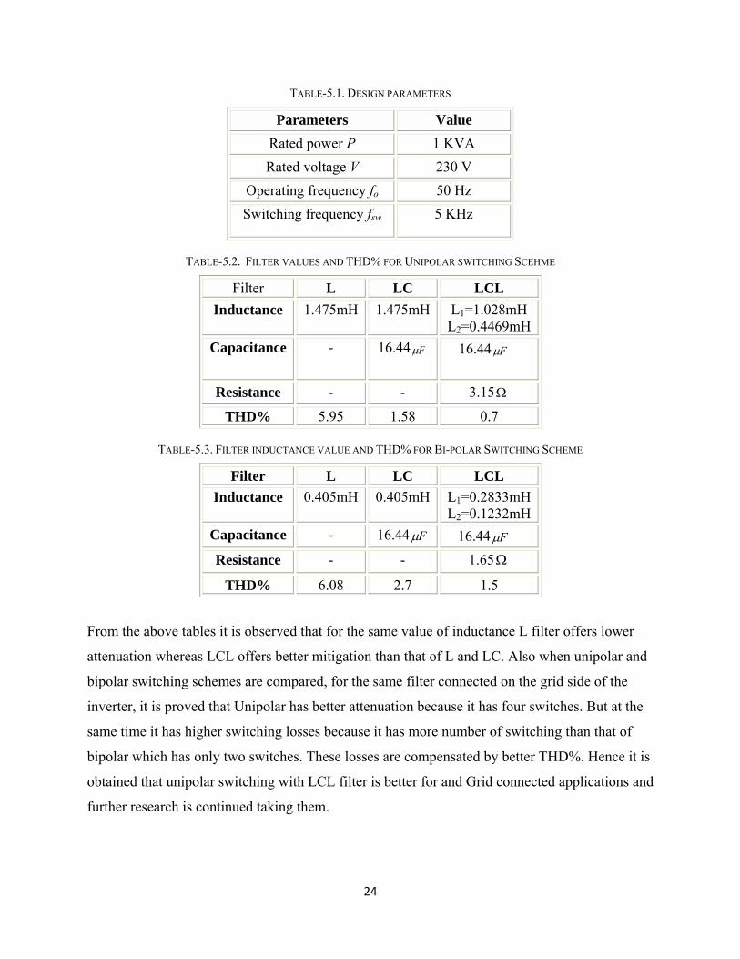
TABLE-5.1. DESIGN PARAMETERS (24)
TABLE-5.2. FILTER VALUES AND THD% FOR UNIPOLAR SWITCHING SCHEME (24)
TABLE-5.3. FILTER INDUCTANCE VALUE AND THD% FOR BI-POLAR SWITCHING SCHEME (24)
TABLE-5.4.: POWER LOSSES IN FILTER (25)
TABLE 5.5.TOTAL LOSSES WITH THD% VARIATION (26)

xi
ABBREVIATIONS AND ACRONYMS
THD – Total Harmonic Distortion
PWM – Pulse Width Modulation
VSI – Voltage Source Inverter
RMS – Root Mean Square

1
CHAPTER 1
Introduction

2
1.1 MOTIVATION:
For past couple of decades, energy demand has increased dramatically and also amount of fossil
fuels has been depleting to a minimum extent. In addition to that environmental pollution has
also been increased due to CO2 emissions from the conventional power plants namely: thermal
and nuclear plants As a result, non conventional energy sources of energy such as solar, wind,
and geothermal have gained popularity now a days. But the conversion efficiency of these
sources is very less which leads to a very high cost of production. Taking the case of a photo-
voltaic system, the cost of PV panel is very high and at the same time the energy conversion is
15-20%. In addition to that there are losses that further occur in converting the current so that it
can be fed to the grid. Also during this conversion process, an inverter that is used to convert DC
to AC introduces harmonics to the grid side current which may lead to the damage of the load.
So, design of a filter is necessary to remove these harmonics. Also, power loss reduction is
needed to improve the efficiency of the system.
1.2 INTRODUCTION:
The key issues like future energy demand, environmental problems and depletion of
fossil fuels have become Global Issue at present scenario. There are different schedules to
provide solution to these problems. Short term energy schedule and Mid-term energy schedule
are to save and use the energy efficiently. But our goal is to provide solution for a long term. The
long term energy schedule is to produce energy by using renewable energy sources such as wind,
solar, fuel cell etc [1]. Renewable energies are clean and green energies. It depends upon the
sources e.g. more wind power can be extracted when there is continuous and strong blow of wind
and solar energy is extracted more during midday. As a result, this type of dispersed power
generating system causes the power quality problems to the utility grid. Power electronics
converter is key component to interface renewable energy source (RES) with utility grid to
satisfy the grid code requirements [2]. Hence these converters are usually connected to the grid
through a simple L filter to reduce the AC side current harmonic, in order to meet corresponding
harmonic standards, however, a larger volume of inductance result in deterioration of system
dynamic response cost. Also such a filter is bulky, inefficient and cannot meet the regulatory
requirements regarding interconnection of harmonic loads to grid [3].
3
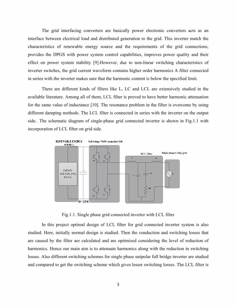
The grid interfacing converters are basically power electronic converters acts as an
interface between electrical load and distributed generation to the grid. This inverter match the
characteristics of renewable energy source and the requirements of the grid connections,
provides the DPGS with power system control capabilities, improves power quality and their
effect on power system stability [9].However, due to non-linear switching characteristics of
inverter switches, the grid current waveform contains higher order harmonics A filter connected
in series with the inverter makes sure that the harmonic content is below the specified limit.
There are different kinds of filters like L, LC and LCL are extensively studied in the
available literature. Among all of them, LCL filter is proved to have better harmonic attenuation
for the same value of inductance [10]. The resonance problem in the filter is overcome by using
different damping methods. The LCL filter is connected in series with the inverter on the output
side.. The schematic diagram of single-phase grid connected inverter is shown in Fig.1.1 with
incorporation of LCL filter on grid side.
Fig.1.1. Single phase grid connected inverter with LCL filter
In this project optimal design of LCL filter for grid connected inverter system is also
studied. Here, initially normal design is studied. Then the conduction and switching losses that
are caused by the filter are calculated and are optimized considering the level of reduction of
harmonics. Hence our main aim is to attenuate harmonics along with the reduction in switching
losses. Also different switching schemes for single phase unipolar full bridge inverter are studied
and compared to get the switching scheme which gives lesser switching losses. The LCL filter is

4
designed accordingly and optimal inductance and capacitance values are obtained. All the related
models are simulated using the MATLAB software and graphs are studied.
1.3 LITERATURE REVIEW:
The importance of renewable energy sources is given by [1]. The paper [3] gave the initial idea
of filter of why it is used how it is to be connected. Then the further study continued when the
more about single phase inverters is studied in [5]. Reference [4]-[7] aided in the comparative
study between unipolar and bipolar switching schemes and also in the study where LCL filter is
proved to be a better one in attenuating higher order harmonics. Later in this work, the filter
design is optimized by following the work of [11] taking the losses caused by the filter. Further
research continued to reduce the switching loss of the inverter [12] so that the efficiency of the
whole system is increased. One can reduce the switching losses by simply applying soft
switching scheme but the external components that are used are sometimes of higher rating than
that of the switches of the inverter and hence soft switching is not a better option. It is important
that the inverter supplies appropriate voltage and frequency waveform in island mode. The
voltage must comply with amplitude and frequency conditions regardless of the type of load
connected. In order to study the stability of the system, transfer function is found out by making
small signal analysis [15].
1.4 ORGANIZATION OF THESIS:
The thesis is organized as follows. Chapter 1 presents the introduction about the project
followed by the thesis objectives.
Chapter 2 deals with Mathematical modelling of the inverter so that the peak to peak
current and the RMS current on the output side of the inverter can be calculated. Also different
inverters like full bridge inverter with unipolar switching scheme and half bridge inverter with
bipolar switching scheme are compared with their respective output current harmonics present in
order to find out which one is better suitable for grid connected applications.
Chapter 3 includes the filter design. Initially different types of filters with their
drawbacks that lead to the introduction of the next one are studied and then, the final LCL filter

5
is designed. Then the damping methods to reduce the resonance effect caused in the filter are
studied. And then the final optimal filter design which gives lower losses at the THD% which is
accepted by Grid code requirements is designed.
Chapter 4 discusses different switching schemes and the scheme that provides lesser
losses is studied. Then the switching frequency waveform and the losses curve are plotted to
compare with the other methods.
Chapter 5 presents the different output waveforms and graphs. Initially the current
waveforms are studied and then the losses and the THD% graph to optimize the filter design are
plotted and then switching frequency and losses graphs are plotted and then analyzed.
Chapter 6 provides the conclusions that derived from the whole project. It shows which
control action is to be selected and what filter is to be selected and the damping method that suits
the required needs is found out. Then the future work is discussed.

6
CHAPTER 2
Mathematical Modelling of Single Phase Voltage Source
Inverter

7
2.1 MATHEMATICAL MODELLING:
2.1.1 Unipolar Switching Scheme:
The schematic diagram of full bridge inverter topology is illustrated in Fig.2.1 The grid voltage is assumed to be sinusoidal. Thus the fundamental component is shown by
(2.1)
The full bridge topology shows us the unipolar switching action, the output is either high to zero or low to zero, rather than high to low as shown in Fig 2.2.
is on when >
is on when - <
is on when >
is on when - <
Fig.2.1. Shows the topology for single phase full bridge inverter
1S evsin triv
2S evsin triv
3S evsin triv
4S evsin triv
0 0 =−= e vv

8
Fig.2.2 Output voltage and current waveform of unipolar switching scheme inverters.
In this reverence, analyzes of switching ripple current on the grid-side filter is presented here
a. Calculation of ripple current and its RMS value
When the switching frequency swf is higher than the operating frequency of , then the inverter
output is regarded to be constant during the switching interval sT . Therefore, the filter inductor current is found to be a triangular waveform as shown in Fig.2.2 (a) for full-bridge topology. The inductor for unipolar PWM can be measured by
(2.2)
(2.3)
savdc
pp TdL
VVii
2')(
2 max−
=Δ=
(2.4)
Replacing the above equation with the following three equations:
, (2.5)
,)()( 1 dcav VtdtV ωω = (2.6)
avdc VVontime
iL −=
Δ max2
sTdontime2'
=
)sin()( tVte dc ωμω =
where
Therefor
Fig.2.3voltage asame as bounded
current ri
Fig .2.
)(' td μω =
μ
)( ti pp ω =Δ
,
is the modul
e the equatio
Fig.2.3. M
3. shows theand current w
that of durby /ppiΔ±
ipple for filte
4. Typical fi
)sin( tωμ for
sin(1(2L
TV sdc μ−
πω << t0
lation index.
on changes t
agnitude dis
e magnitudewaveforms aring2 as depicte
er design is
ilter inductor
)sin())( tt ωμω
00
5
10
15
20
25
Vdc
Ts/8
L
πω << t0
.
to,
stribution of
e distributionare half-wav
[5].The riped in Fig.2.4
shown in Fig
r ripple curr
pi/2utility ang
π
9
∆ipp unipola
n of ∆ipp forve symmetrypple current4. The corre
g.2.5.
ent of IΔ of .8.0=μ
2gle (rad)
ar switching
r unipolar sy, the situatiot consisted
esponding R
f single-phase
pi
scheme for
witching schon during of several
RMS calculat
e full-bridge
π
μ =0.8
heme. Since re
triangular wtion of switc
e inverter wh
πωπ 2<< t
(2.7)
(2.8)
e, the epeats waves ching
hen
10
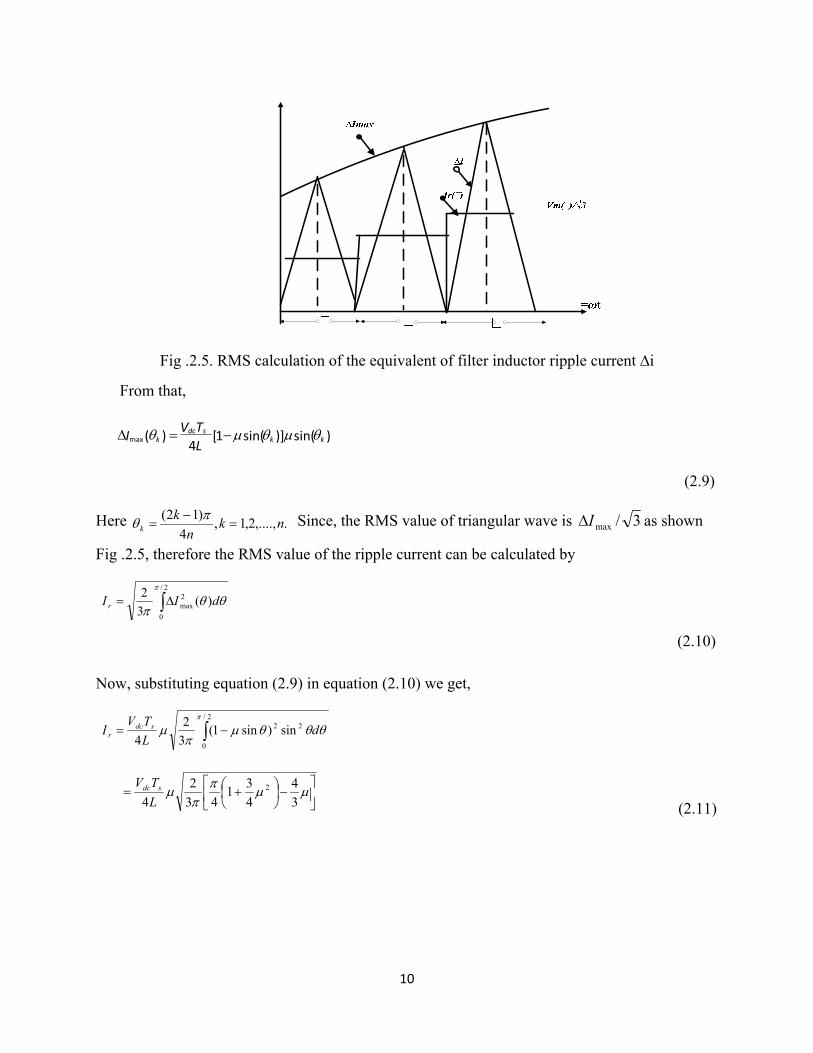
Fig .2.5. RMS calculation of the equivalent of filter inductor ripple current ∆i
From that,
(2.9)
Here .,....,2,1,4
)12( nkn
kk =
−=
πθ Since, the RMS value of triangular wave is 3/maxIΔ as shown
Fig .2.5, therefore the RMS value of the ripple current can be calculated by
∫ Δ=2/
0
2max )(
32 π
θθπ
dII r
(2.10)
Now, substituting equation (2.9) in equation (2.10) we get,
∫ −=2/
0
22 sin)sin1(32
4
π
θθθμπ
μ dLTV
I sdcr
(2.11)
⎥⎦
⎤⎢⎣
⎡−⎟
⎠⎞
⎜⎝⎛ += μμπ
πμ
34
431
432
42
LTV sdc
)sin()] sin(1[4
)(max k k sdc
k L T V
I θ μ θ μ θ −=Δ

11
2.1.2 Bipolar Switching Scheme:
The topology of bridge that is shown in fig.2.1 can also be used as a half bridge topology if the
second leg of the full bridge is not used and the node is directly connected to the split of the DC
source near the ground [4].
Fig.2.6. Output voltage and current waveform of bipolar switching scheme inverters
Fig.2.6 illustrates the principle of sinusoidal bipolar PWM using half bridge inverter topology. When the instantaneous value of the sine reference is larger than the triangular carrier signal, the output is at +Vdc/2 and –Vdc/2 for vice-versa.
The filter inductor current is found to be a triangular waveform as shown in Fig.2.6. for a bipolar switching action.
Therefore the peak to peak current can be derived similar to that of unipolar switching just by replacing by . And it is calculated to be
(2.12)
Fig.2.7.Magnitude distribution of ∆ipp bipolar switching scheme for μ =0.8
dcV 2/dcV
)}(sin1{4
)( 22 tLTV
ti sdcpp ωμω −=Δ
0 pi/2 pi2
2.5
3
3.5
4
4.5
5
5.5
6
6.5
7
utility angle (rad)
Vdc
Ts/4
L

Fig.2
RMS vacalculate
=8L
TVI dc
r
2.8 Response
alue of the swed for unipol
⎢⎣
⎡⎜⎝⎛ −1
31 μ
LTs
e of typical f
witching rippar switching
⎥⎦
⎤⎟⎠⎞+ 42
83 μμ
filter inductoinverte
ple current ing and it is fou
12
or ripple currer when
n half-bridgeund out to be
=μ
rent of IΔ of
e inverters cae
8.0f single-phas
an be calcula
se half-bridg
ated as it is
(
ge
2.13)

13
CHAPTER 3
LCL Filter design

14
3.1 Types of filter:
3.1.1 L filters:
Firstly an L filter is a simple filter designed to mitigate the harmonics in the grid side current.
But there are many drawbacks of L filter like poor system dynamics, low attenuation and long
time response. In order to improve the mitigation level, we have to either increase the value of
the inductor or increase switching frequency where both of them cause increased losses.
3.1.2 LC filters:
A shunt element is added to an L filter to improve the attenuation of the switching frequency
components. Since a capacitance gives low reactance at the high switching frequency it is
selected as the shunt element. But it is observed that the load impedance across the capacitor is
very high.
3.1.3 LCL filters:
It provides better decoupling between the filter and the grid impedance. It also has better
attenuation ratio with smaller values of L and C. Hence LCL filter is designed for grid connected
applications. Resonance is the main problem with LCL filter and it can be damped either by
using active damping methods or passive damping methods. But for grid connected applications
passive damping method is necessary in case when inverter is switched off and filter is still
connected to the grid.
3.2 LCL filter design with passive damping
Here a resistor is connected in series with the capacitor as a part of passive damping scheme. Table-1 shows the details of the data used for calculation of filter inductor value [6].
b
dc
base
dc
LV
ZV
I2221 π
μμ==
(3.1)
Therefore, the switching ripple for full-bridge topology can be calculated by
1I
IRF rsw = ⎥
⎦
⎤⎢⎣
⎡−⎟
⎠⎞
⎜⎝⎛ += μμπ
πμ
34
431
432
42
LTV sdc
bdc
LTVμ
π 22

15
(3.2)
For half-bridge topology switching ripple current can be calculated as
(3.3)
(3.4)
where, P
VZbase
2
= and
The resonant frequency should be in the range 10 ωo< ωres< (ωsw/2) which is an important condition for filter inductor design. Table-5.2 and Table-5.3 gives the typical filter with their % THD values of grid currents.
22 VP
VQC
oo
ref ω
αω
== (3.5)
(3.6)
3.3 Optimal LCL Filter design
The design of the LCL filter should also consider the selection of resonance frequency ( ).The resonance frequency depends upon the circuit elements. So, the resonance frequency range to be selected to avoid resonance problems,
210 0
swres
ωωω ≤≤ (3.7)
Where, is utility frequency and is switching frequency.
Passive damping is adopted for grid connected applications since when inverter is switched off still there will be a capacitor to provide the continuity of supply.
TT
RFLL s
swb⎥⎦
⎤⎢⎣
⎡−⎟
⎠⎞
⎜⎝⎛ +≥ μμππ
34
431
431 2
1II
RF rsw = ⎟
⎠⎞
⎜⎝⎛ +−= 42
831
31
8μμ
LTV sdc
bdc
LTVμ
π 24
TT
RFLL s
swb2
222
6)8/31(1
μμμπ +−
≥
o
baseb f
ZL
π2=
P%5.2=α
fresCR
ω31
=

16
Fig.3.1.LCL filter design with passive damping
Resonance frequency is given by the equation,
LCr12 =ω (3.8)
Where L= L1 + L2 and C= C1 + Cf
The relation between L1 and L2 is given by L1= aLL2 and between C1 and Cf is given by Cf=aCC1
Determination of aL and aC:
1) Generally L1 and L2 remains same and hence aL=1 2) The selection of aC is tradeoff between effective damping and power loss in shunt
damping circuit. So, to get aC we use the following transfer function,
)1
11()1(
5.05.0)()(
2
2
32
232
acRCj
jRCjuju
rf
r
f
i
+−+−
+=
ωωω
ωω
ωωω
(3.9)
To find the Q-factor,
5.0lim 0 =→i
c
uu
ω (3.10)
c
cfr
fr
i
c
aaRCj
RCjuu
r
+
+=
=
1
5.05.0
3
3
ω
ω
ωω
(3.11)
Dividing (3.11) by (3.10) we get,
17
2
2
3
3
)1(
11
)(
c
cfr
c
cfr
c
aaRCj
aaRCj
aQ
+
++
=ω
ω (3.12)
Fig.3.2.Variation of Q-factor in terms of ac
Losses increases with increase in ac and hence the optimal value of ac is found out to be 1 as studied in [10]
3.3.1 Power losses in the damping Circuit:
The power loss in the damping circuit is calculated as shown below. The losses at switching frequency and fundamental frequency are only calculated because other harmonics do not contribute much to the losses. Power losses are calculated for p.u. and then actual values are calculated for a given base value.
i) Fundamental frequency power loss:
[ ]*)50( Re dcd IUalP = (3.13)
31 RsCsC
UIf
fcd +
= (3.14)
23
2250
35050
1)1(
RCRCjCj
UIf
ffcd ω
ωω+
−= (3.15)
23
2250
322
502
)50( 1 RCRCU
Pf
fcd ω
ω
+= (3.16)
0 1 2 3 4 5 6 7 8 9 100
10
20
30
40
50
60
70
80
90
ac
Q-fa
ctor

18
Where ω50 is fundamental frequency in p.u.(rad/sec), Uc is 1 p.u.
ii) Switching frequency power loss:
Grid is considered as a short circuit at the switching frequency but it is an ideal voltage at fundamental frequency. So at switching frequency Ug=0,
)1
11()1(
5.05.0
2
2
32
23
cr
swfsw
r
sw
fswic
aRCj
RCjUU
+−+−
+=
ωω
ωωω
ω (3.17)
23
223
1)(
RCjRCC
UIfsw
fswfswcd ω
ωω+
+= (3.18)
(3.19)
Representing Uc and Id as complex fractions,
jdcjbaUU ic +
+= (3.20)
)(1 222 jyx
RCCUI
ddsw
dswcd +
+=
ωω
(3.21)
*23
22** )(1
)( jyxRC
CjdcjbaU
jdcjbaUIU
fsw
fswiidc +
+++
++
=ωω
(3.22)
[ ] xRC
CdcbaUIUalP
fsw
fswidcswd 2
32222
22*
)( 12Re
ωω
+++
== (3.23)
Here,
0.5 , 0.5 , 1 , 1 , , 1
3.3.2Power losses in the inductor:
The power losses in the inductor are calculated using the software called Magnetic design where the inputs given are inductor value, peak to peak current and RMS current of the ripple.

19
CHAPTER 4
Switching loss reduction with LCL filter

20
4.1 DIFFERENT SWITCHING METHODS:
One more losses that has major contribution to the losses in the inverter system is Switching
losses of the switches used in the system. Three different methods are studied to reduce the
losses and the one that is giving lower switching losses is selected. The equations are adopted
from [13]
The switching loss for one cycle is assumed to be directly proportional to current [12].
Therefore, the average switching loss per cycle can be calculated as
)()(
)( 1
tTtiK
tqs
sub ωω
ω = (4.1)
Where K is a constant that depends upon DC voltage, i1 is instantaneous current and Ts is
switching period. Since, we are going to vary switching frequency in different methods, here
Ts(wt) is taken as a function.
The switching losses can be given as
)()sin(2
)( 1
tTtIK
tqs
sub ωφω
ω−
= (4.2)
Where φ is the lagging angle of the grid current.
The average switching losses for a cycle can be derived as follows,
∫=π
ωωπ
ω0
)(1))(( tdtqtTQ subs (4.3)
= tdtT
tIK
s
ωω
φωπ
π
∫−
0
1
)()sin(2 (4.4)
4.1.1 Constant switching frequency:
In this case we take constant switching frequency. Therefore Ts (wt) remains constant. The
switching losses graph would be a sinusoidal plot.

21
)sin(2))(( 1 φωω −= tT
IKtTqs
s (4.5)
a. Constant ripple scheme:
In this case we take constant required rms current ripple. From that value peak to peak ripple is
calculated,
reqrmspkpk II ,32 Δ=Δ − (4.6)
We know that ∆Ipk-pk as derived in [14]
)sin()).sin(1(2
)( tmtmLTVti aa
sdcpp ωωω −=Δ (4.7)
Hence Ts(wt) is derived from above equation,
tmtmVLI
tTaad
reqrmss ωωω
sin)sin1(32
)( ,
−Δ
= (4.8)
Therefore,
tmtmtLI
VIKtTq aareqrms
ds ωωφωω sinsin1)sin(
322))((
,
1 −−Δ
= (4.9)
4.2 REDUCTION OF SWITCHING LOSSES
4.2.1 Optimal Switching scheme:
In this method, the value or function of )( tTs ω is selected such that the switching losses are
lower. As derived in [11],
31
22' )
)sin()sin1()sin(
()(tmtm
tCtT
aas ωω
φωω
−−
= (4.10)
Where,

22
∫ −−
Δ=
π
ωωωφωπ 0
31
222
,'
})(sin)sin1()]{[sin(1
32
tdttmtmV
LIC
aad
reqrms (4.11)
Substituting the above function of )( tTs ω in )( tqsub ω we get the expression for switching loss,
'
32
32
32
1 sinsin1)sin(2))((
CtmtmtIK
tTq aas
ωωφωω
−−= (4.12)

23
CHAPTER 5
Simulation Results and Discussions
24
TABLE-5.1. DESIGN PARAMETERS
Parameters Value Rated power P 1 KVA Rated voltage V 230 V
Operating frequency fo 50 Hz Switching frequency fsw 5 KHz
TABLE-5.2. FILTER VALUES AND THD% FOR UNIPOLAR SWITCHING SCEHME
Filter L LC LCL Inductance 1.475mH 1.475mH L1=1.028mH
L2=0.4469mH Capacitance - 16.44 Fμ
16.44 Fμ
Resistance - - 3.15Ω
THD% 5.95 1.58 0.7
TABLE-5.3. FILTER INDUCTANCE VALUE AND THD% FOR BI-POLAR SWITCHING SCHEME
Filter L LC LCL Inductance 0.405mH 0.405mH L1=0.2833mH
L2=0.1232mH Capacitance - 16.44 Fμ 16.44 Fμ Resistance - - 1.65Ω
THD% 6.08 2.7 1.5
From the above tables it is observed that for the same value of inductance L filter offers lower
attenuation whereas LCL offers better mitigation than that of L and LC. Also when unipolar and
bipolar switching schemes are compared, for the same filter connected on the grid side of the
inverter, it is proved that Unipolar has better attenuation because it has four switches. But at the
same time it has higher switching losses because it has more number of switching than that of
bipolar which has only two switches. These losses are compensated by better THD%. Hence it is
obtained that unipolar switching with LCL filter is better for and Grid connected applications and
further research is continued taking them.
25
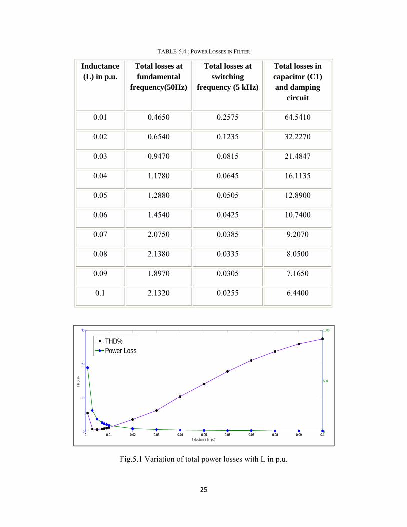
TABLE-5.4.: POWER LOSSES IN FILTER
Inductance (L) in p.u.
Total losses at fundamental
frequency(50Hz)
Total losses at switching
frequency (5 kHz)
Total losses in capacitor (C1) and damping
circuit
0.01 0.4650 0.2575 64.5410
0.02 0.6540 0.1235 32.2270
0.03 0.9470 0.0815 21.4847
0.04 1.1780 0.0645 16.1135
0.05 1.2880 0.0505 12.8900
0.06 1.4540 0.0425 10.7400
0.07 2.0750 0.0385 9.2070
0.08 2.1380 0.0335 8.0500
0.09 1.8970 0.0305 7.1650
0.1 2.1320 0.0255 6.4400
Fig.5.1 Variation of total power losses with L in p.u.
0 0.01 0.02 0.03 0.04 0.05 0.06 0.07 0.08 0.09 0.10
10
20
30
Inductance (in pu)
THD
%
0 0.01 0.02 0.03 0.04 0.05 0.06 0.07 0.08 0.09 0.10
500
1000
THD%Power Loss

26
TABLE 5.5.Total losses with THD% variation
Inductance (L) in p.u.
Total losses of filter
THD%
0.01 65.2635 4.75
0.02 33.0045 1.39
0.03 22.5132 2.48
0.04 17.3560 5.13
0.05 14.2285 7.59
0.06 12.2365 9.69
0.07 11.3205 11.56
0.08 10.2215 13.12
0.09 9.0925 14.43
0.1 8.5975 15.88
Table 5.4 gives the total losses in the filter. With the increase in inductor value, it is observed
that losses at fundamental frequency tend to increase whereas at switching frequency the losses
are reduced. From the above graph an inductor value of 0.02 pu has lower THD% and at the
same time lower losses. But previously we found out that mHL 875.4≥ and also the power losses
tend to decrease with increase in L, but this is limited by the THD%. We cannot increase the
value of L where its THD% increases over 5%. Therefore the inductor value should be less than
19mH where the THD% is 5.13 as per TABLE 5.5. So considering both the factors we therefore
the optimal values are L= 4.875mH, C= 0.149mF and R=5.7199ohm and with THD% of
3.2%.Now different switching methods are studied for inverter with the filter. The values of filter
are taken as derived from the above procedure.
27
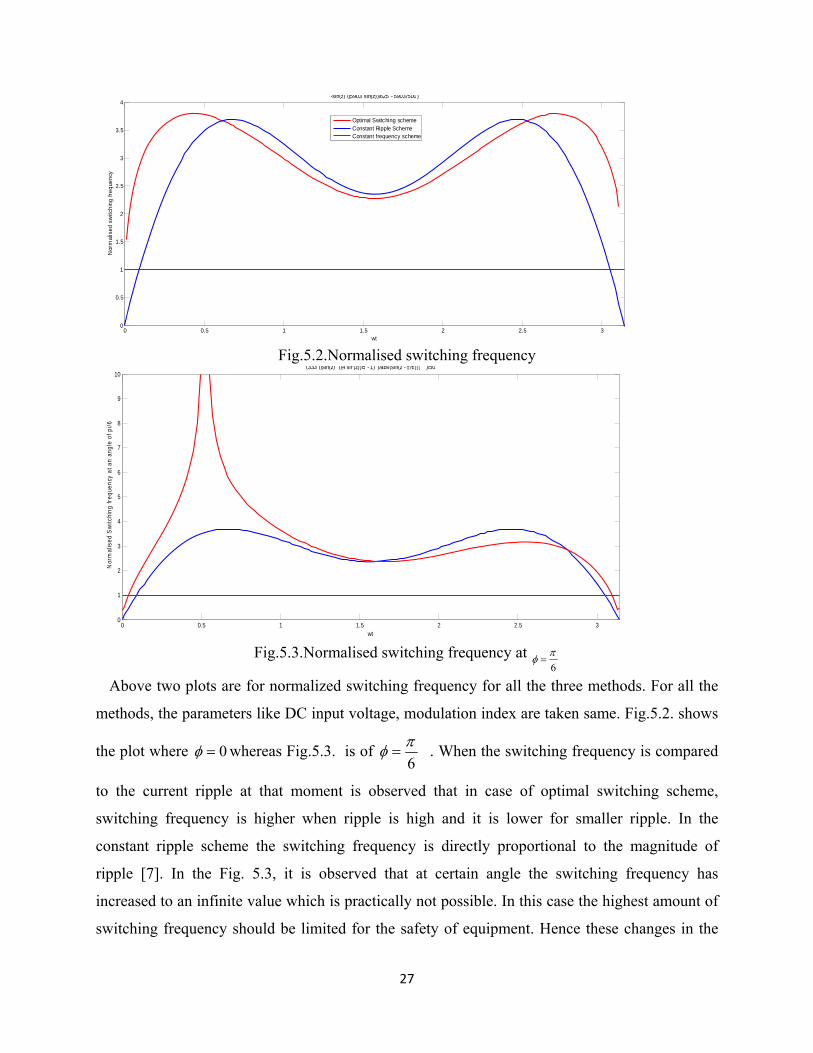
Fig.5.2.Normalised switching frequency
Fig.5.3.Normalised switching frequency at
6πφ =
Above two plots are for normalized switching frequency for all the three methods. For all the
methods, the parameters like DC input voltage, modulation index are taken same. Fig.5.2. shows
the plot where 0=φ whereas Fig.5.3. is of 6πφ = . When the switching frequency is compared
to the current ripple at that moment is observed that in case of optimal switching scheme,
switching frequency is higher when ripple is high and it is lower for smaller ripple. In the
constant ripple scheme the switching frequency is directly proportional to the magnitude of
ripple [7]. In the Fig. 5.3, it is observed that at certain angle the switching frequency has
increased to an infinite value which is practically not possible. In this case the highest amount of
switching frequency should be limited for the safety of equipment. Hence these changes in the
0 0.5 1 1.5 2 2.5 30
0.5
1
1.5
2
2.5
3
3.5
4
wt
-sin(z) ((5903 sin(z))/625 - 5903/500)
Nor
mal
ised
sw
itchi
ng fr
eque
ncy
Optimal Switching schemeConstant Ripple SchemeConstant frequency scheme
0 0.5 1 1.5 2 2.5 30
1
2
3
4
5
6
7
8
9
10
wt
(333 ((sin(z) ((4 sin(z))/5 - 1) )/abs(sin(z - π /6))) )/50
Nor
mal
ised
Sw
itchi
ng fr
eque
ncy
at a
n an
gle
of p
i/6
28
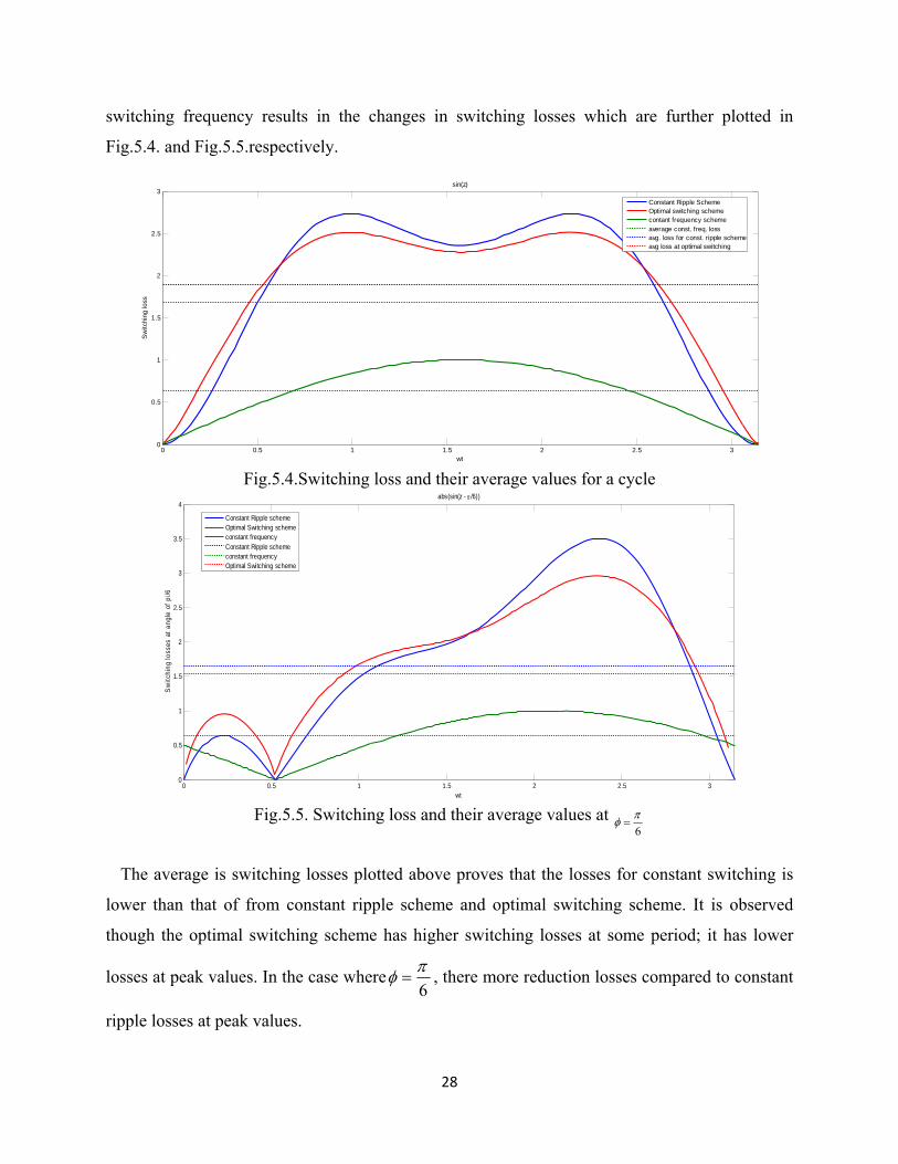
switching frequency results in the changes in switching losses which are further plotted in
Fig.5.4. and Fig.5.5.respectively.
Fig.5.4.Switching loss and their average values for a cycle
Fig.5.5. Switching loss and their average values at
6πφ =
The average is switching losses plotted above proves that the losses for constant switching is
lower than that of from constant ripple scheme and optimal switching scheme. It is observed
though the optimal switching scheme has higher switching losses at some period; it has lower
losses at peak values. In the case where6πφ = , there more reduction losses compared to constant
ripple losses at peak values.
0 0.5 1 1.5 2 2.5 30
0.5
1
1.5
2
2.5
3
wt
sin(z)
Sw
itchi
ng lo
ss
Constant Ripple SchemeOptimal switching schemecontant frequency schemeaverage const. freq. lossavg. loss for const. ripple schemeavg loss at optimal switching
0 0.5 1 1.5 2 2.5 30
0.5
1
1.5
2
2.5
3
3.5
4
wt
abs(sin(z - π /6))
Sw
itchi
ng lo
sses
at a
ngle
of p
i/6
Constant Ripple schemeOptimal Switching schemeconstant frequencyConstant Ripple schemeconstant frequencyOptimal Switching scheme

29
CHAPTER 6
Conclusions and
Future work

30
6.1 CONCLUSIONS:
In this project the optimal design of LCL filter and switching loss reduction in grid
connected inverter system is studied. From the study, the following observations are made. LCL
filter can provide good grid synchronization without knowledge of grid impedance. Furthermore,
The RMS calculation of the switching ripple current can be used for loss calculation of grid-
connected single-phase inverter systems. The agreement with the simulation results to a
prodigious extent with a good sinusoidal current, a lesser harmonic component is obtained. An
optimal LCL filter design along with switching loss reduction is done. Hence, the optimal filter
is designed considering THD% and ripple factor. And for that value of inductor different
switching losses are studied. It is found that for grid connected system where switching of
inverter is very low, constant switching scheme has much lower losses compared to the other two
methods. But, during load variation there would be variation in switching frequency and hence
constant frequency cannot be maintained. In order overcome this draw back one can employ
adaptive hysteresis control in the inner feedback control loop which is also called constant ripple
scheme. However, it is found that optimal switching scheme gives lesser switching losses and
maintaining of constant switching frequency is beyond the scope of this project.
6.2 FUTURE WORK:
Further this work can be continued simulating the closed loop response and improving the whole
performance of the system. Also now-a-days active damping is also applied for grid connected
applications, which provide lesser filter without resonance problem.
31
REFERENCES
[1] M. Singh, V. Khadkikar, A. Chandra, R.K. Varma, “Grid interconnection of Renewable Energy sources at the distribution level with power quality improvement features,” IEEE Transactions on Power Delivery, vol.26, no.1, pp.307-315, Jan. 2011.
[2] F.Blaabjerg, Z. Chen, and S. B. Kjaer, “Power Electronics as Efficient Interface in Dispersed Power Generation Systems,” IEEE Trans., Power Electron., vol. 19, no. 5, pp. 1184–1194, Sep. 2004.
[3] Hanju Cha, T.K. Vu, "Comparative Analysis of Low-pass Output Filter for Single-phase Grid-connected Photovoltaic Inverter," Proc. of IEEE Applied Power Electronics Conference and Exposition, 2010, pp. 1659-1665.
[4] Yaosuo Xue; Liuchen Chang, Sren Baekhj Kjaer, J. Bordonau; T. Shimizu, “Topologies of single-phase inverter for small distributed power generators: an overview”, IEEE Transactions on Power Electronics, vol. 19, pp 1305–1314.
[5] Hyosung Kim, Kyoung-Hwan Kim, “Filter design for grid connected PV inverters”, Proc. of IEEE International Conference on Sustainable Energy Technologies, ICSET200), pp.1070-1075, 2008.
[6] Parikshith.B.C, Dr.Vinod John,”Higher order output filter design for grid connected Power Converters,” Proc. of Fifteenth National Power Systems Conference NPSC 2008, IIT Bombay, December 2008.
[7] L Umanand,”Power Electronics: Essentials & Applications”, Wiley Publications, 2009. First Edition.
[8] Blaabjerg, F.; Teodorescu, R.; Liserre, M.; Timbus, A.V., “Overview of Control and Grid Synchronization for Distributed Power Generation Systems” IEEE Transactions on Industrial Electronics,Vol.:53 ,Issue:5,2006 , Page(s): 1398 – 1409.
[9] Lingrong Zeng, Liuchen Chang, “Improved Current controller Based on SVPWM for Three-Phase Grid-Connected Voltage Source Inverters” Proc. of IEEE PESC '05. Page(s): 2912 – 2917.
[10] Lingrong Zeng, Liuchen Chang, “Improved Current controller Based on SVPWM for Three-Phase Grid-Connected Voltage Source Inverters” Proc. of IEEE PESC '05. Page(s): 2912 – 2917.
[11] E.Twining and D. G. Holmes, “Grid current regulation of a three-phase voltage source inverter with an LCL input filter,” IEEE Trans. Power Electron., vol. 18, no. 3, pp. 888– 895, May 2003.
[12] Cannegowda, P.; John, V.; , "Filter Optimization for Grid Interactive Voltage Source Inverters," Industrial Electronics, IEEE Transactions on , vol.57, no.12, pp.4106-4114, Dec. 2010.
[13] Xiaolin Mao; Ayyanar, R.; Krishnamurthy, H.K.; , "Optimal Variable Switching Frequency Scheme for Reducing Switching Loss in Single-Phase Inverters Based on Time-Domain Ripple Analysis," Power Electronics, IEEE Transactions on , vol.24, no.4, pp.991-1001, April 2009.
[14] J.W.Kolar, H. Ertl, and F.C. Zach, “Influence of the modulation method on the conduction and switching losses of a PWM converter system,” IEEE Trans. Ind. Appl. ,vol.27,no.6,pp. 1063-1075, Nov,/Dec. 1991.

32
[15] Hyosung Kim, Kyoung-Hwan Kim, “Filter design for grid connected PV inverters”, IEEE International Conference on Sustainable Energy Technologies (ICSET2008), pp. 1070-1075, 2008.
[16] R.Ortega, E. Figueres, G.Garcera, C.L. Trujillo, D.Velasco, “Control techniques for reduction of the total harmonic distortion in voltage applied to a single phase inverter with non linear loads: Review,” Renewable and Sustainable Energy Reviews 16(2012) 1754-1761.

33
APPENDIX

34
A. SMALL SIGNAL OF SINGLE PHASE VSI:
Case 1:
When switches S1 and S2 are ON the resulting circuit will be as shown in Fig.A.1.
Fig.A.1. when S1 and S2 switches are ON
The calculations of small signal modeling are adopted from [15]. Applying KVL in the above circuit
(A.1)
(A.2)
(A.3)
Case 2:
When switches S3 and S4 are ON, the resulting circuit will be fig.A.2.
By applying KVL in the above circuit,
(A.4)
And
(A.5)

35
Vdc
iL iC i0
Rc
C
Fig.A.2. when switches S3 and S4 are ON
(A.6)
Let’s consider average value of the inductor current and capacitor voltage over a switching period Ts.
′ (A.7)
Where d= duty cycle, and d’=1-d
And
C i ′ i (A.8)
Lets define an operating point as follows
Duty cycle =D
Input Voltage = Vdc
Output Voltage = V0
Capacitor Voltage = VC
Inductor current = IL
Source current = Is
In order to design a small signal model we will have to consider a small perturbation along with its steady state values
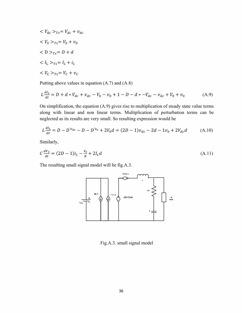
36
D
L
C
Putting above values in equation (A.7) and (A.8)
1 (A.9)
On simplification, the equation (A.9) gives rise to multiplication of steady state value terms along with linear and non linear terms. Multiplication of perturbation terms can be neglected as its results are very small. So resulting expression would be
′ ′ 2 2 1 2 1 2 (A.10)
Similarly,
2 1 2 (A.11)
The resulting small signal model will be fig.A.3.
Fig.A.3. small signal model

37
B. INDUCTOR FILTER DESIGN:
Relationship between flux, mmf and permeance is [7].
iN ..Λ=φ (B.1)
Differentiating the above equation and multiplying with N
dtdiN
dtdN 2.Λ=φ
(B.2)
dtdiL
dtdiNe =Λ= 2.
(B.3)
m
cro
lNA
NL2
2.μμ
=Λ=
(B.4)
As we know inductor is used as an energy storing device, therefore,
22
2 .21
21
21 mmf
NmmfLLiEl Λ=⎟
⎠⎞
⎜⎝⎛==
(B.5)
An air gap is generally introduced for inductive applications wherein the core needs to store energy which is known as fringing model [5, 6].
ρ=
(B.6)
VKVAI f ××
=9.03
LfjIE fl π2×= (B.7)
(B.8)
(B.9)
⎟⎟⎠
⎞⎜⎜⎝
⎛+=+ g
r
m
coco
g
cro
m ll
AAl
Al
μμμμμ1
mcw
lcwp JBKK
EAAA
2==
grm
cro
llA
μμμ+
=Λ

38
, (B.10)
According to the values of and the core is selected and the inductor is designed.
Λ=
LNJ
Ia rms=
ml pA

39
PAPERS PUBLISHED
1. Debati Marandi, Naga Sowmya Tontepu, B.Chitti Babu, ” Comparative Study between Unipolar and Bipolar Switching Scheme with LCL Filter for Single-Phase Grid Connected Inverter System”, In Proc. IEEE Students’ Conference on Electrical, Electronics and Computer Sciences 2012 (SCEECS 2012), MANIT, Bhopal, Mar/2012-Received Best Paper Award
2. Naga Sowmya Tontepu, Debati Marandi, B.Chitti Babu, “ Optimal filter design and Switching loss reduction in grid connected inverter system”, In Proc. IEEE 2nd Students’ Conference on Engineering and Systems 2013 (SCES 2013), MNNIT, Allahabad, Apr/2013.
3. Debati Marandi, Naga Sowmya Tontepu, B.Chitti Babu, “LCL Filter Response of 1-Ф Grid Interactive Inverter using Small Signal Modelling”, In Proc. IEEE Sponsorded 1st National Conference on Power Electronics Systems & Applications (PESA 2013), NIT, Rourkela, pp.181-184, March/2013.