Optical spectroscopy of InGaAs quantum dots394191/FULLTEXT01.pdf · Journal: Physical Review B, 78,...
64
Linköping studies in science and technology dissertation no. 1363 Optical spectroscopy of InGaAs quantum dots Arvid Larsson Semiconductor materials division Department of physics, chemistry and biology (IFM) Linköping 2011
Transcript of Optical spectroscopy of InGaAs quantum dots394191/FULLTEXT01.pdf · Journal: Physical Review B, 78,...

Linköping studies in science and technology dissertation no. 1363
Optical spectroscopy of InGaAs quantum dots
Arvid Larsson
Semiconductor materials division Department of physics, chemistry and biology (IFM)
Linköping 2011

Copyright © 2011 Arvid Larsson unless otherwise noted
ISBN: 978-91-7393-238-7 ISSN: 0345-7524
Printed by LiU-Tryck, Linköping, Sweden, 2011
III
Abstract
The work presented in this thesis deals with optical studies of semiconductor quantum dots (QDs) in the InGaAs material system. It is shown that for self-assembled InAs QDs, the interaction with the surrounding GaAs barrier and the InAs wetting layer (WL) in particular, has a very large impact on their optical properties. The ability to control the charge state of individual QDs is demonstrated and attributed to a modulation in the carrier transport dynamics in the WL. After photo-excitation of carriers (electrons and holes) in the barrier, they will migrate in the sample and with a certain probability become captured into a QD. During this migration, the carriers can be affected by exerting them to an external magnetic field or by altering the temperature. An external magnetic field applied perpendicular to the carrier transport direction will lead to a decrease in the carrier drift velocity since their trajectories are bent, and at sufficiently high field strength become circular. In turn, this decreases the probability for the carriers to reach the QD since the probability for the carriers to get trapped in WL localizing potentials increases. An elevated temperature leads to an increased escape rate out of these potentials and again increases the flow of carriers towards the QD. These effects have significantly different strengths for electrons and holes due to the large difference in their respective masses and therefore it constitutes a way to control the supply of charges to the QD. Another effect of the different capture probabilities for electrons and holes into a QD that is explored is the ability to achieve spin polarization of the neutral exciton (X0). It has been concluded frequently in the literature that X0 cannot maintain its spin without application of an external magnetic field, due to the anisotropic electron – hole exchange interaction (AEI). In our studies,
IV
we show that at certain excitation conditions, the AEI can be by-passed since an electron is captured faster than a hole into a QD. The result is that the electron will populate the QD solely for a certain time window, before the hole is captured. During this time window and at polarized excitation, which creates spin polarized carriers, the electron can polarize the QD nuclei. In this way, a nuclear magnetic field is built up with a magnitude as high as ~ 1.5 T. This field will stabilize the X0 spin in a similar manner as an external magnetic field would. The build-up time for this nuclear field was determined to be ~ 10 ms and the polarization degree achieved for X0 is ~ 60 %. In contrast to the case of X0, the AEI is naturally cancelled for the negatively charged exciton (X-) and the positively charged exciton (X+) complexes. This is due to the fact that the electron (hole) spin is paired off in case of X- (X+). Accordingly, an even higher polarization degree (~ 73 %) is measured for the positively charged exciton. In a different study, pyramidal QD structures were employed. In contrast to fabrication of self-assembled QDs, the position of QDs can be controlled in these samples as they are grown in inverted pyramids that are etched into a substrate. After sample processing, the result is free-standing AlGaAs pyramids with InGaAs QDs inside. Due to the pyramidal shape of these structures, the light extraction is considerably enhanced which opens up possibilities to study processes un-resolvable in self-assembled QDs. This has allowed studies of Auger-like shake-up processes of holes in single QDs. Normally, after radiative recombination of X+, the QD is populated with a ground state hole. However, at recombination, a fraction of the energy can be transferred to the hole so that it afterwards occupies an excited state instead. This process is detected experimentally as a red-shifted luminescence satellite peak with an intensity on the order of ~ 1/1000 of the main X+ peak intensity. The identification of the satellite peak is based on its intensity correlation with the X+ peak, photoluminescence excitation measurements and on magnetic field measurements.

V
Populärvetenskaplig sammanfattning
Arbetet som presenteras i denna avhandling rör studier av kvantprickars optiska egenskaper. En kvantprick är en halvledarkristall som endast är några tiotals nanometer stor. Den ligger oftast inbäddad inuti en större kristall av ett annat halvledarmaterial och pga. den begränsade storleken får en kvantprick mycket speciella egenskaper. Bland annat så kommer elektronerna i en kvantprick endast att kunna anta vissa diskreta energinivåer liknande situationen för elektronerna i en atom. Följaktligen kallas kvantprickar ofta för artificiella atomer. För halvledarmaterial gäller det generellt att det inte endast är fria elektroner i ledningsbandet, som kan leda ström utan även tomma elektrontillstånd i valensbandet, vilka uppträder som positivt laddade partiklar, kan leda ström. Dessa kallas kort och gott för hål. I en kvantprick har hålen såsom elektronerna helt diskreta energinivåer. Precis som är fallet i en atom, så kommer elektroniska övergångar mellan olika energinivåer i en kvantprick att resultera i att ljus emitteras. Energin (dvs. våglängden alt. färgen) för detta ljus bestäms av hur energinivåerna i kvantpricken ligger, för elektronerna och hålen, och genom att analysera ljuset kan man således studera kvantprickens egenskaper. Studierna i den här avhandlingen visar att växelverkan mellan en kvantprick och den omgivande kristallen, som den ligger inbäddad i, har stor inverkan på kvantprickens optiska egenskaper. T.ex. visas att man kan kontrollera antalet elektroner, som kommer att finnas i kvantpricken genom att modifiera hur elektronerna kan röra sig i omgivningen. Dessa rörelser modifieras här genom att variera temperaturen och genom att lägga på ett magnetiskt fält. Ett magnetiskt fält, vinkelrätt mot en elektrons rörelse, kommer att böja av dess bana och dess chans att nå fram till kvantpricken kan således minskas.

VI
Elektronen kan då istället fastna i andra potentialgropar i kvantprickens närhet. Genom att öka temperaturen, vilket ger elektronerna större energi, kan deras chans att nå fram till kvantpricken å andra sidan öka. En annan effekt, som studerats, är möjligheten att kontrollera spinnet hos elektronerna i en kvantprick. Även i dessa studier visar det sig att växelverkan med omgivningen spelar stor roll och kan användas till att kontrollera elektronens spin. Mekanismen som föreslås är att om elektronerna hinner före hålen till kvantpricken, så hinner de överföra sitt spin till atomkärnorna i kvantpricken. På detta sätt kan man få atomkärnornas spin polariserat, vilket resulterar i ett inbyggt magnetfält, i storleksordningen 1.5 Tesla, som i sin tur hjälper till att upprätthålla en hög grad av spinpolarisering även hos elektronerna. För att få elektronerna att hinna först, måste deras rörelser i omgivningen kontrolleras. I en ytterligare studie undersöktes den process där en elektronisk övergång i kvantpricken inte enbart resulterar i emission av ljus, utan även i att en annan partikel tar över en del av energin och blir exciterad. Dessa processer avspeglas i att en del av det ljus som emitteras har lägre energi. Detta ljus är också mycket svagt, ca 1000 ggr lägre intensitet, och möjligheten att kunna mäta detta är helt beroende på hur ljusstarka kvantprickarna är. De prover som använts i denna studie består av pyramidstrukturer, ca 7.5 mikrometer stora, med kvantprickar inuti. Denna geometri ger ca 1000 ggr bättre ljusutbyte jämfört med traditionella strukturer, vilket möjliggjort studien.

VII
Preface
This doctorate thesis concerns optical studies of semiconductor quantum dots in the InGaAs material system. The studies were carried out between August 2005 and December 2010 within the Semiconductor Materials Division at the Department of Physics, Chemistry and Biology (IFM) at Linköping University. The thesis is divided into two parts. The first part is supposed to serve as an introduction to the research field as chapters 1 - 3 give introductions to semi-conductors, quantum dots and photoluminescence, respectively. The second part starts with chapter 4, which is a summary of the subsequent collection of seven papers that constitute the scientific output of the work. The following pages involve a list of the included and excluded papers as well as contributions to international conferences. For the seven papers included in this thesis, I have indicated my contribution to the work.

VIII
Papers included in the thesis -------------------- Paper 1. Title: Effective tuning of the charge state of a single InAs/GaAs quantum dot by an external magnetic field Authors: E. S. Moskalenko, L. A. Larsson, M. Larsson, P. O. Holtz, W. V. Schoenfeld and P. M. Petroff Journal: Physical Review B, 78, 075306 (2008) My contribution: I did all the measurements together with the first author, who wrote the first draft of the manuscript, which I edited and finalized. -------------------- Paper 2. Title: Comparative Magneto-Photoluminescence Study of Ensembles and of Individual InAs Quantum Dots Authors: E. S. Moskalenko, L. A. Larsson, M. Larsson, P. O. Holtz, W. V. Schoenfeld and P. M. Petroff Journal: Nano Letters, 9, 353 (2009) My contribution: I did all the measurements together with the first author, except the data for Fig. 2 that was measured by the first and third author. The first author wrote the first draft of the manuscript, which I edited and finalized. -------------------- Paper 3. Title: Temperature and Magnetic Field Effects on the Transport Controlled Charge State of a Single Quantum Dot Authors: L. A. Larsson, M. Larsson, E. S. Moskalenko and P. O. Holtz Journal: Nanoscale Research Letters, 5, 1150 (2010) My contribution: I did all the measurements together with the third author, except the data for Fig. 1, which I measured myself. I wrote the manuscript. -------------------- Paper 4. Title: Spin polarization of the neutral exciton in a single InAs quantum dot at zero magnetic field Authors: E. S. Moskalenko, L. A. Larsson and P. O. Holtz Journal: Physical Review B, 78, 193413 (2009) My contribution: I realized the experimental approach to Fig. 2 and I did all the measurements together with the first author who wrote the first draft of the manuscript, which I edited and finalized.

IX
-------------------- Paper 5. Title: Spin polarization of neutral excitons in quantum dots: the role of the carrier collection area Authors: E. S. Moskalenko, L. A. Larsson and P. O. Holtz Journal: Nanotechnology, 21, 345401 (2010) My contribution: I did the measurements for Fig. 1 together with the first author who did the measurements for Fig. 2 - 3 himself. The first author wrote the first draft of the manuscript, which I edited and finalized. -------------------- Paper 6. Title: Manipulating the Spin Polarization of Excitons in a Single Quantum Dot by Optical Means Authors: L. A. Larsson, E. S. Moskalenko and P. O. Holtz Journal: Applied Physics Letters - Accepted My contribution: I did all the measurements together with the second author who wrote the first draft of the manuscript, which I re-wrote and finalized. -------------------- Paper 7. Title: Hole shake-up in individual InGaAs quantum dots Authors: L. A. Larsson, K. F. Karlsson, D. Dufåker, V. Dimastrodonato, L. O. Mereni, P. O. Holtz, and E. Pelucchi Manuscript My contribution: I did all the measurements and wrote the manuscript. --------------------
Papers not included in the thesis -------------------- Paper 8. Title: Magnetic Field Effects on Optical and Transport Properties in InAs/GaAs Quantum Dots Authors: M. Larsson, E. S. Moskalenko, L. A. Larsson, P. O. Holtz, C. Verdozzi, C.-O. Almbladh, W. V. Schoenfeld, P. M. Petroff Journal: Physical Review B, 74, 245312 (2006)
X
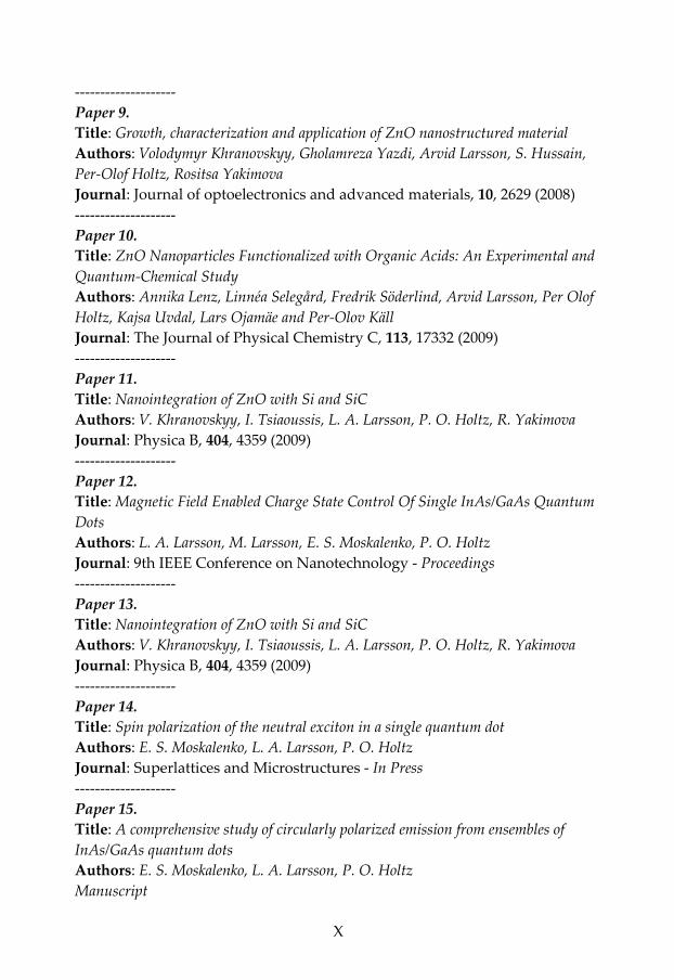
-------------------- Paper 9. Title: Growth, characterization and application of ZnO nanostructured material Authors: Volodymyr Khranovskyy, Gholamreza Yazdi, Arvid Larsson, S. Hussain, Per-Olof Holtz, Rositsa Yakimova Journal: Journal of optoelectronics and advanced materials, 10, 2629 (2008) -------------------- Paper 10. Title: ZnO Nanoparticles Functionalized with Organic Acids: An Experimental and Quantum-Chemical Study Authors: Annika Lenz, Linnéa Selegård, Fredrik Söderlind, Arvid Larsson, Per Olof Holtz, Kajsa Uvdal, Lars Ojamäe and Per-Olov Käll Journal: The Journal of Physical Chemistry C, 113, 17332 (2009) -------------------- Paper 11. Title: Nanointegration of ZnO with Si and SiC Authors: V. Khranovskyy, I. Tsiaoussis, L. A. Larsson, P. O. Holtz, R. Yakimova Journal: Physica B, 404, 4359 (2009) -------------------- Paper 12. Title: Magnetic Field Enabled Charge State Control Of Single InAs/GaAs Quantum Dots Authors: L. A. Larsson, M. Larsson, E. S. Moskalenko, P. O. Holtz Journal: 9th IEEE Conference on Nanotechnology - Proceedings -------------------- Paper 13. Title: Nanointegration of ZnO with Si and SiC Authors: V. Khranovskyy, I. Tsiaoussis, L. A. Larsson, P. O. Holtz, R. Yakimova Journal: Physica B, 404, 4359 (2009) -------------------- Paper 14. Title: Spin polarization of the neutral exciton in a single quantum dot Authors: E. S. Moskalenko, L. A. Larsson, P. O. Holtz Journal: Superlattices and Microstructures - In Press -------------------- Paper 15. Title: A comprehensive study of circularly polarized emission from ensembles of InAs/GaAs quantum dots Authors: E. S. Moskalenko, L. A. Larsson, P. O. Holtz Manuscript
XI
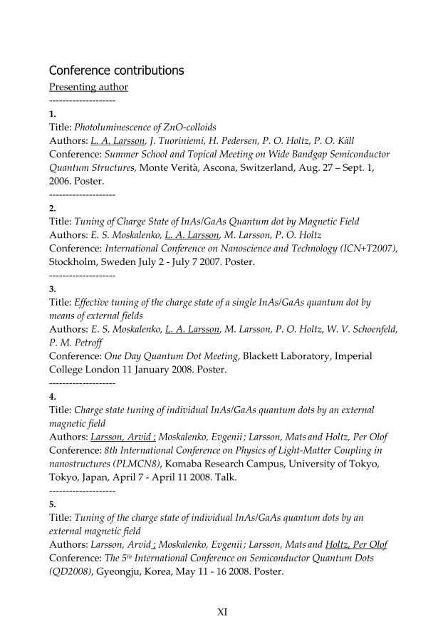
Conference contributions Presenting author -------------------- 1. Title: Photoluminescence of ZnO-colloids Authors: L. A. Larsson, J. Tuoriniemi, H. Pedersen, P. O. Holtz, P. O. Käll Conference: Summer School and Topical Meeting on Wide Bandgap Semiconductor Quantum Structures, Monte Verità, Ascona, Switzerland, Aug. 27 – Sept. 1, 2006. Poster. -------------------- 2. Title: Tuning of Charge State of InAs/GaAs Quantum dot by Magnetic Field Authors: E. S. Moskalenko, L. A. Larsson, M. Larsson, P. O. Holtz Conference: International Conference on Nanoscience and Technology (ICN+T2007), Stockholm, Sweden July 2 - July 7 2007. Poster. -------------------- 3. Title: Effective tuning of the charge state of a single InAs/GaAs quantum dot by means of external fields Authors: E. S. Moskalenko, L. A. Larsson, M. Larsson, P. O. Holtz, W. V. Schoenfeld, P. M. Petroff Conference: One Day Quantum Dot Meeting, Blackett Laboratory, Imperial College London 11 January 2008. Poster. -------------------- 4. Title: Charge state tuning of individual InAs/GaAs quantum dots by an external magnetic field Authors: Larsson, Arvid ; Moskalenko, Evgenii ; Larsson, Mats and Holtz, Per Olof Conference: 8th International Conference on Physics of Light-Matter Coupling in nanostructures (PLMCN8), Komaba Research Campus, University of Tokyo, Tokyo, Japan, April 7 - April 11 2008. Talk. -------------------- 5. Title: Tuning of the charge state of individual InAs/GaAs quantum dots by an external magnetic field Authors: Larsson, Arvid ; Moskalenko, Evgenii ; Larsson, Mats and Holtz, Per Olof Conference: The 5th International Conference on Semiconductor Quantum Dots (QD2008), Gyeongju, Korea, May 11 - 16 2008. Poster.
XII
-------------------- 6. Title: Charge State Control Of Single InAs/GaAs Quantum Dots By Means Of An External Magnetic Field Authors: L. A. Larsson, E. S. Moskalenko, M. Larsson, P. O. Holtz Conference: 29th International Conference on the Physics of Semiconductors (ICPS2008), Rio de Janeiro, Brazil, July 27 - August 1 2008. Talk / Paper. -------------------- 7. Title: Magnetic Field Enabled Charge State Control Of Single InAs/GaAs Quantum Dots Authors: L. A. Larsson, M. Larsson, E. S. Moskalenko, P. O. Holtz Conference: 9th IEEE Conference on Nanotechnology, (IEEE NANO 2009), Genoa, Italy, July 26 - 30 2009. Talk / Paper. -------------------- 8. Title: Spin polarization of the neutral exciton in a single quantum dot Authors: E. S. Moskalenko, L. A. Larsson and P. O. Holtz Conference: 10th International Conference on Physics of Light-Matter Coupling in nanostructures (PLMCN10) Cuernavaca, Mexico, April 12 - April 16 2010. Talk / Paper. -------------------- 9. Title: Controlling the charge state of a single quantum dot by means of temperature and external magnetic field Authors: E. S. Moskalenko, L. A. Larsson and P. O. Holtz Conference: 10th International Conference on Physics of Light-Matter Coupling in nanostructures (PLMCN10) Cuernavaca, Mexico, April 12 - April 16 2010. Talk. -------------------- 10. Title: Spin polarizing neutral excitons in quantum dots Authors: L. A. Larsson, E. S. Moskalenko and P. O. Holtz Conference: 30th International Conference on the Physics of Semiconductors (ICPS2010) COEX, Seoul, Korea, July 25 - July 30 2010. Talk. -------------------- 11. Title: Quantum dot charging by means of temperature and magnetic field Authors: L. A. Larsson, E. S. Moskalenko and P. O. Holtz Conference: 30th International Conference on the Physics of Semiconductors (ICPS2010) COEX, Seoul, Korea, July 25 - July 30 2010. Poster.
XIII
Acknowledgements
I want to express my gratitude to my supervisor, Prof. Per Olof Holtz. Thank you for letting me participate in your interesting research projects, for generously sharing your experience and knowledge, and for believing in me. You have an exceptional talent for inspiration and encouragement in situations that appear miserable to others - like me. I’m also very grateful to my assistant supervisor, Doc. Fredrik Karlsson. Thank you for always having time to discuss any question or issue that comes up, huge or insignificant. Thank you for kindly sharing your insights in quantum dot physics, computation techniques and spectroscopy. I would like to thank Dr. Evgenii Moskalenko for our very fruitful collaboration. During all the time spent with you in the lab, I have learnt a great deal of physics. Thanks to Dr. Mats Larsson for teaching me a lot about how to use the lab equipment. Thanks to both of you for your earlier works on these dots. Thank you Associate Prof. Plamen Paskov, for your help with various experimental issues, especially the numerous laser re-alignments, and for your catching laughs in the lab. Thanks to Associate Prof. Qingxiang Zhao for your elucidating chats about ZnO and about experimental approaches. I would also like to acknowledge Prof. Bo Monemar and Prof. Erik Janzén, who have headed the Semiconductor Materials Division (former Materials Science Division), for the enriching research climate in this group. I am grateful to Arne Eklund and Roger Carmesten for help with all sorts of technical problems and for keeping the helium bottles full.

XIV
Thanks to Eva Wibom for taking care of all administrative matters, for organizing our group conferences, and for your patience with my fill-in-form-ignorance. Thanks to Louise Gustafsson-Rydström for ensuring a good working climate and for caring for everyone at this big department. Special thanks to Chih-Wei, Dao and Daniel Dufåker for your quantum dot-collaboration and positive spirit in the PL-lab. Thanks Daniel, for the long but rewarding days, evenings, nights and mornings we spent in total darkness. I want to thank Dr. Johan Eriksson, together with whom I initialized my explorations of quantum dot physics, and Andreas Gällström for all enlightening discussions about pretty much everything. Thanks to Dr. Linda Höglund for your inspiring works on QDIPs and old wooden houses. Thank you Dr. Patrick Carlsson for letting me participate in transporting your chest of drawers up the stairs and Dr. Henrik Pedersen for all the comforting lunch chats. I also acknowledge Prof. Anne Henry, Doc. Urban Forsberg, Doc. Carl Hemmingsson, Doc. Galia Pozina, Dr. Volodymyr Khranovskyy, Dr. Daniel Dagnelund, Dr. Stefano Leone, Anders, Daniel N., Ted, Franziska, Jan and all other colleges for making the time at IFM truly memorable. Finally, I want to thank my big, loving family. I thank my parents, bonus-parents, sisters and brother for always supporting me and my interest in science and for always caring for me. Thanks to my parents-, sisters- and brother-in-law for your warmth and kindness. Special thanks for helping out with babysitting during my thesis writing. Naima, my dear daughter. Thank you for your genuine enthusiasm to almost everything. Your attitude is my ideal. Thank you for making me so proud. Dear Sofia. Thank you for your endurance over the last months, for your unfailing support and for your endless encouragement. We did this together. Thank you for sharing your life with me, I’m the luckiest guy. I love you so. There are many people that I should thank. Probably some names that should have been mentioned here were not. Forgive me. I’m truly grateful, I promise.
/Arvid

XV
Table of contents
ABSTRACT ................................................................................................................................III
POPULÄRVETENSKAPLIG SAMMANFATTNING ........................................................ V
PREFACE .................................................................................................................................. VII Papers included in the thesis ..........................................................................................................................VIII Papers not included in the thesis .......................................................................................................................IX Conference contributions ...................................................................................................................................XI
ACKNOWLEDGEMENTS...................................................................................................XIII
1 SEMICONDUCTOR PHYSICS....................................................................................... 1
1.1 Electronic structure and energy bands ...................................................................................................1 1.1.1 Metals, insulators and semiconductors...............................................................................................2 1.1.2 Crystal structure.....................................................................................................................................3 1.1.3 Reciprocal lattice ....................................................................................................................................5 1.1.4 Bloch’s theorem and band structure....................................................................................................6 1.1.5 The effective mass and envelope function approach ........................................................................8 1.1.6 The valence band structure...................................................................................................................9
1.2 Optical properties and excitons.............................................................................................................10 1.2.1 Excitons .................................................................................................................................................10 1.2.2 Impurity related emission...................................................................................................................11 1.2.3 Non-radiative recombination .............................................................................................................12 1.2.4 Shake-up processes ..............................................................................................................................13
1.3 Optical orientation...................................................................................................................................13 1.3.1 Nuclear spin..........................................................................................................................................14 1.3.2 Electron - nuclear spin interaction.....................................................................................................14 1.3.3 Optical pumping of nuclear spin .......................................................................................................15

XVI
2 QUANTUM DOTS .......................................................................................................... 17
2.1 Heterostructures .......................................................................................................................................17 2.1.1 Quantum structures and the density of states .................................................................................18 2.1.2 The quantum well ................................................................................................................................19
2.2 Excitons in quantum dots .......................................................................................................................20 2.2.1 The neutral exciton - bright and dark................................................................................................21 2.2.2 The bi-exciton .......................................................................................................................................22 2.2.3 Charged excitons..................................................................................................................................22 2.2.4 Excited exciton states...........................................................................................................................23
2.3 Fabrication of quantum dots ..................................................................................................................24 2.3.1 Stranski-Krastanow growth................................................................................................................24 2.3.2 Inverted pyramid growth ...................................................................................................................25
2.4 Carrier capture and transport.................................................................................................................26 2.4.1 The role of the wetting layer...............................................................................................................27 2.4.2 Electric field effects ..............................................................................................................................27
2.5 Magnetic field effects ..............................................................................................................................28 2.5.1 Magnetic moment ................................................................................................................................28 2.5.2 Magnetic confinement .........................................................................................................................29
2.6 Applications of quantum dots ...............................................................................................................30
3 PHOTOLUMINESCENCE.............................................................................................. 31
3.1 Conventional photoluminescence.........................................................................................................31
3.2 Micro-photoluminescence ......................................................................................................................33
3.3 Photoluminescence excitation................................................................................................................36
3.4 Magneto-photoluminescence.................................................................................................................37
3.5 Polarization optics....................................................................................................................................38
4 SUMMARY OF THE PAPERS....................................................................................... 41
BIBLIOGRAPHY....................................................................................................................... 43
INDEX ......................................................................................................................................... 47

1
1 Semiconductor physics
1.1 Electronic structure and energy bands In a single atom, the electrons orbiting the nucleus can only occupy certain discrete energy levels. This was first realized by Niels Bohr (Nobel price 1922) in the early nineteen hundreds, when he introduced what nowadays is referred to as the Bohr model of the atom, see Fig. 1.1(a). An electron can be excited from a certain energy level to a higher energy level by absorbing a photon and correspondingly, an excited electron can relax to a lower energy level by emitting a photon. The energy of such an emitted photon is given by the energy difference between the initial and final energy levels and hence, is characteristic for the atom type. In a crystal, where the atoms are arranged in a periodic lattice, the outermost electrons are shared between several atoms and their allowed energies are no longer discrete. Instead, bands of allowed electron energies are formed, as illustrated in Fig. 1.1(b).
Figure 1.1. (a) A schematic illustration of the Bohr model of the single atom electron levels. (b) The transition into electron energy bands in a crystal.

2
The shaded regions of Fig. 1.1(b) represent the allowed energy levels for electrons in the crystal and the regions between the allowed energy bands are forbidden, i.e. no electrons can have such energies in the crystal. These gaps in the energy continuum for electrons are the band gaps of the material. It should be noted that the outermost electron levels in semiconductors are of either s-type or p-type [1] , hence the notation in Fig. 1.1(b). Figure 1.2 illustrates the electronic s- and p-orbitals.
Figure 1.2. Illustration of s-type and p-type atomic orbitals.
1.1.1 Metals, insulators and semiconductors When an allowed energy band is completely filled with electrons, no net electron movement is possible since an electron can only move into an empty state. This is a consequence of electrons being fermions that obey the Pauli exclusion principle which dictates that two electrons can not have the same set of quantum numbers. The energy band that is completely filled with electrons at temperature T = 0 K in a material is called the valence band, while the next energy band is called the conduction band. A material in which the conduction band is only partially filled can easily conduct current and is called a metal. A material for which the valence band is completely filled and the conduction band is empty has a very large resistivity and is called an insulator or a semiconductor. The difference between an insulator and a semiconductor is mainly the width of the band gap; an insulator has a much larger band gap than a semiconductor. The band gap between the valence band and the conduction band is denoted Eg and is a crucial material parameter when dealing with semiconductor characterization. The band gaps, at room temperature, of the materials explored in this work are given in Table 1.1.

3
InAs GaAs AlAs
0.36 eV 1.42 eV 2.36 eV Table 1.1. Band gap of InAs, GaAs and AlAs.
A semiconductor has vanishing conductivity at T = 0 K and limited conductivity at elevated temperatures, but it is possible to controllably alter the conductivity by many orders of magnitude, e.g. by an applied voltage or by impurity doping . This is the reason for the great impact of semiconductors on the development of electronic components [2]. In analogy to the atom case, an electron can be excited from the valence band to the conduction band by absorbing a photon. The empty state thereby created in the valence band is referred to as a hole. A valence band hole acts like a positively charged particle and can be ascribed various particle properties like mass and momentum. Electrons and holes are collectively referred to as charge carriers. An electron in the conduction band can recombine with a hole in the valence band and emit a photon. The energy of the emitted photon is characteristic for the band gap of the material but one should also take into account different Coulomb effects as described in sections 1.2.1 and 1.2.2.
1.1.2 Crystal structure When atoms are put together to form a solid, they will be arranged in a certain lattice in such a way that it minimizes the energy of the crystal. It is the inter-atomic forces and the size of the constituent atoms that will determine the crystal structure. Naturally, the crystal structure of a given material is of fundamental importance for its electronic properties. The semiconductors explored in this work, i.e. InAs, GaAs and AlAs and their ternary alloys such as InGaAs and AlGaAs, all crystallize in the zinc-blend structure. To illustrate the zinc-blend structure, we first consider a face centered cubic (FCC) lattice, which is a cubic lattice with one atom at each corner of the cube, and one atom at each face of the cube, as depicted in Fig. 1.3(a). The side length of the cube is called the lattice constant and is denoted a. The zinc-blend lattice consists of two interpenetrating FCC lattices, of different atomic species,

4
with one displaced from the other by a quarter of the lattice constant along the cube diagonal, see Fig. 1.3(b).
Figure 1.3. Illustration of (a) FCC lattice and (b) zinc-blend lattice.
The lattice constants, at room temperature, for the semiconductors studied in the present work are given in Table 1.2.
InAs GaAs AlAs 6.058 Å 5.653 Å 5.661 Å
Table 1.2. Lattice constants for InAs, GaAs and AlAs [2]. In the case that two interpenetrating FCC lattices consist of the same kind of atoms, the result is a diamond lattice, in which the very important semiconductor silicon (and others) crystallizes. Directions in a cubic lattice are described by giving the Cartesian vector components within square brackets, such as [100], [010], and [001] for directions along the x-, y-, and z-axis respectively, see Fig. 1.3(a). A crystal plane perpendicular to the direction [abc] is written within parenthesizes, (abc), and a family of equivalent planes within curly brackets, e.g. {abc}.

5
1.1.3 Reciprocal lattice For a theoretical exploration of the physics of crystalline solids, one must employ quantum mechanics. Since a quantum mechanical treatment often involves wave physics, it turns out to be favorable to convert the description of the crystal lattice, from real space into the reciprocal space. The reason is that in reciprocal space (or “k-space”) the length unit is equivalent to the wave vector unit. The reciprocal lattice of a FCC lattice is the body centered cubic (BCC) lattice, which is a cubic lattice with one atom at each corner of the cube, and one at the cube center, see Fig. 1.4(a)
Figure 1.4. Illustration of a BCC lattice (a) and the Brillouin zone for a zinc-blend crystal (b) with the notation for the most important crystallographic symmetry points.
An entire crystal can be described simply as a repetition of the smallest unit cell. The first Brillouin zone is the unit cell of the reciprocal lattice. For the zinc-blend crystal structure it is illustrated in Fig. 1.4(b). The origin in reciprocal space is called the Γ-point.

6
1.1.4 Bloch’s theorem and band structure The impact that the crystal periodicity has on the electron energy levels, is nicely illustrated by introducing a periodic potential into the time-independent one-dimensional Schrödinger equation, Eq. (1.1) [1, 3].
( ) ( ) ( ) ( )xExxUdx
xdm
ψψψ =+− 2
22
2 (Eq. 1.1)
Here ħ is Planck’s constant over 2π, m is the particle mass, )(xψ is the wave function for the particle, U(x) is the potential in which the particle is moving and E is its energy. For a free particle, i.e. when U(x) = 0, the wave function xkiex ⋅⋅=)(ψ is a solution to Eq. 1.1 and the electron is delocalized. The resulting dispersion relation, i.e. the relationship between the electron’s wave vector, k, and its energy, is given by Eq. 1.2 where m0 = 9.11·10-31 kg is the free electron mass. This dispersion relation is parabolic as depicted in Fig. 1.5(a).
0
22
2mkE = (Eq. 1.2)
When instead considering an electron in a lattice it should, due to the periodicity of the crystal lattice, have a periodic probability density distribution so that ( ) ( ) 22 axx += ψψ . Such a wave function can be achieved by multiplying the free electron wave, xkie ⋅⋅ , with a function, ( )xuk containing the periodicity of the lattice:
( ) ( ) xkikk exux ⋅⋅⋅=ψ (Eq. 1.3a)
with ( ) ( )axuxu kk += (Eq. 1.3b)
Eq. 1.3a and b are equivalent to Eq. 1.4.
( ) ( ) akikk exax ⋅⋅⋅=+ ψψ (Eq. 1.4)

7
Here, akie ⋅⋅ constitutes a phase factor with period 2π/a. The dispersion relation for an electron in a periodic potential is depicted in Fig. 1.5(b) and it is seen that it is no longer continuous but instead shows band gaps in between the allowed energy bands. Normally, the dispersion relation is plotted in the reduced zone scheme so that k is restricted to the range - π/a < k < π/a. This is achieved by subtracting a multiple of 2π/a from k if it lies outside this range. The multiple, often denoted n, is called the band index. Fig. 1.5(c) shows the dispersion relation in the reduced zone scheme. Unlike the free electron case, the product ħk is not equal to the momentum for electrons in a crystal. However, it has many similarities and is therefore referred to as crystal momentum. Equation 1.3a is known as Bloch’s theorem and has proven extremely useful when dealing with electronic bands in solids. To analyze and understand the relation between energy and momentum of electrons in a crystal, it is now only necessary to treat the smallest unit cell of k-space, i.e. the Brillouin zone, Fig. 1.4(b), thanks to the periodicity introduced by Eq. 1.4.
Figure 1.5. Dispersion relation for (a) a free electron and (b) an electron in a periodic potential. (c) is the same as (b) but in a reduced zone scheme.
The dispersion relation is what will determine much of an electron’s properties, such as the response to an applied electric field and interactions with photons and phonons. This relationship is the band structure of the material and it is visualized by plotting E vs. k in different crystal directions, as in Fig. 1.6 for the case of InAs.

8
Figure 1.6. Band structure of InAs. Freely from Ref. [4].
1.1.5 The effective mass and envelope function approach In many semiconductors and in particular the ones treated here1, the conduction band has its minimum and the valence band its maximum at the Γ-point, i.e. at k = 0. Thus, this is where most optical transitions will occur and hence the band structure profile around the Γ-point is of great importance. In the effective mass approach the dispersion relation for an electron in a crystal is approximated with a parabola, according to Eq. 1.5 which is an acceptable approximation close to the Γ-point, see Fig. 1.6. The curvature of this parabola is not the same as for a free electron (Eq. 1.2) but instead corresponds to a different, effective, electron mass (m*) in the material.
( ) *
22
2mkkE = (Eq. 1.5)
In the effective mass approximation, the Schrödinger equation is re-written in the envelope function approximation in which the wave function is replaced with an envelope function, )(rχ , that is slowly varying on the range of the lattice constant [1, 3].
1For AlxGa1-xAs with x ≳ 0.45 the CB minimum changes from Γ to X and the band gap is indirect.

9
1.1.6 The valence band structure In case of the conduction band, which is made up of s-type atomic orbitals, the quadratic dispersion relation given by Eq. 1.5 is a fair approximation in the vicinity of the Γ-point. However in the valence band case, it should be appended with additional information about the bands before being employed. The valence band is made up of p-type atomic orbitals and therefore has an associated orbital angular momentum, l = 1. In a given direction (say z), l is quantized and takes the values lz = - ħ, 0 and + ħ. These states are denoted by the magnetic quantum number ml = -1, 0 and 1, respectively. In addition, each electron has a spin, s, which is quantized and takes the values sz = ± 1/2ħ. The spin and the orbital angular momentum will interact because when the motion of a charged particle results in an angular momentum, it will also result in a magnetic dipole. This dipole will interact with the electron spin and cause a fine-structure splitting of the two electron levels with spins parallel and anti-parallel to the dipole. This effect is referred to as spin-orbit coupling. The total angular momentum for an electron is denoted j = l + s, which is then j = 3/2 or 1/2. For j = 3/2 its z-projection takes the values jz = -3/2ħ, -1/2ħ, 1/2ħ and +3/2ħ and for j = 1/2 its projection is jz = -1/2ħ or 1/2ħ. As a result, the valence band has three subbands as listed below which are denoted the heavy hole (HH), light hole (LH) and spin-orbit split-off (SO) band. (j, jz) = (3/2, ±3/2) - the heavy hole (HH) subband (j, jz) = (3/2, ±1/2) - the light hole (LH) subband (j, jz) = (1/2, ±1/2) - the spin-orbit split-off (SO) subband The HH and LH bands are degenerate at the Γ-point (see Fig. 1.6), whereas the SO band is offset by the split-off energy, ΔSO. In a strained crystal, e.g. a quantum structure, the HH and LH bands will also split at the Γ-point. Since the curvature of the dispersion relation (Eq. 1.5) is inversely proportional to the effective mass of the particle, holes in the HH, LH and SO bands will respond as having different effective masses, hence the names “heavy” and

10
“light” hole. The magnitude of ΔSO and the effective masses at the Γ-point for the materials treated in the present work are given in Table 1.3 [1 - 3, 5, 6].
InAs GaAs AlAs ΔSO 0.28 eV 0.341 eV 0.39 eV me* 0.023 m0 0.063 m0 0.11 m0 mhh* 0.39 m0 0.51 m0 0.76 m0 mlh* 0.026 0.076 m0 0.15 m0
Table 1.3. Split-off energy, ΔSO, and effective masses at the Γ-point for InAs, GaAs and AlAs [5] at room temperature. m0 = 9.11·10-31 kg is the electron rest mass.
1.2 Optical properties and excitons As mentioned above, InAs and GaAs have direct band gap so that the conduction band has its minimum and the valence band has its maximum at the same point in k-space, i.e. at the Γ-point (see Fig. 1.6). Thus, momentum is conserved during an optical transition between the valence band top and the conduction band bottom so that such processes can occur without the involvement of phonons. This is in contrast to other semiconductors such as Si, Ge and GaP, which have indirect band gap. In such materials a transition between the conduction band minimum and the valence band maximum, at different points in k-space, generally requires phonon-assistance since the photon momentum is approximately zero.
1.2.1 Excitons An electron in the conduction band and a hole in the valence band can form a bound state called an exciton. The exciton concept is often introduced as analogous to the hydrogen atom with the proton replaced by a valence band hole [1, 3]. As such, the exciton can be ascribed a binding energy, EB, and a Bohr radius, aexc, according to Eq. 1.6 and Eq. 1.7.
RymEr
rB 2ε
= (Eq. 1.6)

11
r
rBexc m
aa ε= (Eq. 1.7)
Here Ry = 13.6 eV and aB = 0.053 nm is the Rydberg energy and the Bohr radius for the hydrogen atom, respectively. εr is the static dielectric constant of the material and mr is the reduced mass for the electron-hole pair calculated from the effective masses by Eq. 1.8.
**111
her mmm += (Eq. 1.8)
Table 1.4 presents values of εr, mr, EB and aexc. The exciton binding energy is given as a positive number here although it lowers the energy of the electron-hole pair. Thus, in contrast to the recombination (absorption) of a free electron and a free hole, the energy of the emitted (absorbed) photon at the recombination (absorption) of an exciton is lower than the band gap due to the exciton binding, see Fig. 1.7.
InAs GaAs AlAs εr 15.1 13.2 10.1 mr 0.022 0.056 0.096 EB 1.3 meV 4.4 meV 12.8 meV aexc 36.4 nm 12.5 nm 5.6 nm
Table 1.4. Static dielectric constant (εr) [3] along with calculated values of electron-heavy hole reduced mass (mr), exciton binding energy (EB) and exciton Bohr radius (aexc) for InAs, GaAs and AlAs at room temperature (Table 1.3).
1.2.2 Impurity related emission In addition to excitonic binding of electrons and holes, that shifts the emission and absorption energy below the band gap, also impurities such as donors and acceptors will affect the transition energy. Various transitions can be, and have been, studied in optical spectroscopy and some of them are given in Fig. 1.7. They are; Free-to-bound (FB) transition, when an electron (hole) bound to a donor (acceptor) recombines with a free hole (electron).

12
The donor-acceptor-pair (DAP) transition, when an electron bound to a donor recombines with a hole bound to an acceptor. Bound exciton (BE) transition of the donor bound (DB) exciton and the acceptor bound exciton. Optical excitation of the FB transition provides a route to create un-equal numbers of free electrons and holes in the material, which can be used to create charged exciton complexes in quantum dots [7].
Figure 1.7. The most common optical transitions in bulk, direct band gap, semiconductors.
1.2.3 Non-radiative recombination There are alternative ways for an electron-hole pair to recombine than to emit a photon. One example of a non-radiative recombination process is the Auger process. In this process, the energy of the recombining particles is transferred to a third particle, which gains kinetic energy. Other non-radiative recombination processes are related to single- or multiple-phonon emission, either in a cascade or by simultaneous multi-phonon emission. The depletion field, related to surfaces and interfaces, can lead to separation of carriers, preventing radiative recombination. Near the surface of a crystal, there is also an increased density of energy states in the band gap of the material, due to dangling atomic bonds. Impurity defect levels can also act as non-radiative channels, since they may move up and down in the band gap due to crystal vibrations and thereby can capture both electrons and holes [1].

13
1.2.4 Shake-up processes A shake-up process is a combination of a radiative and a non-radiative recombination process. In this case, only a fraction of the energy of the recombining particles is transferred to a third particle and the rest of the energy is emitted as a photon (Fig. 1.8). Hence, these processes can be studied optically, unlike the case for a pure Auger-process (section 1.2.3). The energy difference between the shake-up related emission and the direct emission (without involvement of a third particle) can give information about higher available energy levels into which the third particle is shaken-up. Some of the research results presented in this thesis concerns this kind of shake-up of holes in single quantum dots. The shake-up process is also referred to as a satellite-process and the spectral peak resulting from this process is a satellite-peak. Therefore, the spectroscopic approach to study these processes might be called satellite spectroscopy.
Figure 1.8. A shake-up process. (a) A fraction of the recombination energy is transferred to a third carrier that (b) gets excited.
1.3 Optical orientation In addition to the Pauli exclusion principle (section 1.1.1) and the spin-orbit coupling (section 1.1.6), the spin of electrons in a material will also interact with the spin of the atomic nuclei in the crystal lattice. The significance of this interaction is very dependent on the magnitude of the nuclear spin of the atomic species in the crystal but can in some cases lead to very interesting and useful effects such as optical orientation of nuclear spins [8, 9].

14
1.3.1 Nuclear spin The atomic nucleus consists of protons and neutrons, which are nucleons. The number of protons in a nucleus is denoted Z, the number of neutrons is denoted N and the atomic mass is then Z + N. Just like electrons, the nucleons are fermions with spin, S = 1/2, orbital angular momentum, L, and total angular momentum J = S + L. When putting several protons and neutrons together in an atomic nucleus, the total nuclear angular momentum, referred to as the nuclear spin and denoted I, can take either half-integer or integer values. The way to determine the nuclear spin is found elsewhere [10], but it is interesting to note that both protons and neutrons have a tendency to couple in pairs so that if both Z and N are even, I = 0. If instead both Z and N are odd, the nuclear spin is determined by the coupling of the odd proton and neutron, I = Jp + Jn. The nuclear spins of the atoms encountered in this work are listed in Table 1.5. The large spin of the In-atom is important for some of the research results presented in this thesis, since it allows for the build-up of a nuclear magnetic field with a strength of ~ 1.5 T, due to optical spin pumping, as described in the following sections.
In Ga Al As 9/2 3/2 5/2 3/2
Table 1.5. The nuclear spin, I, of In, Ga, Al and As atoms.
1.3.2 Electron - nuclear spin interaction The hyperfine interaction is the magnetic interaction between electron and nuclear spins. This interaction is written as A·I·s, where A is the hyperfine constant while I and s are the nucleus and electron spin, respectively. A is proportional to the probability for the electron to be at the nucleus. As a consequence of this, and since the valence band states have p-type symmetry (Fig. 1.2), holes will not be coupled to the nuclei through the hyperfine interaction. On the other hand, conduction band electrons (which are s-type, Fig. 1.2) have a significant probability to be at the atomic center and their spin will couple to the nuclear spin. In fact, the hyperfine interaction manifests

15
itself as a mechanism for transferring spin polarization from the electrons to the nuclei.
1.3.3 Optical pumping of nuclear spin A photon has an angular momentum projection, in the direction of light propagation, equal to +ħ or -ħ. A light beam consisting of only one (or at least a very large majority of one) of these two types of photons is circularly polarized. Such a beam is also referred to as σ+- or σ—polarized, if the angular momentum is +ħ or -ħ, respectively. Alternatively the nomenclature right or left handed polarization is also encountered. In such a case, one should carefully define whether the light is seen by an observer from whom or towards whom the light is propagating and unfortunately two opposite reference standards exist in this nomenclature. In the case with a clockwise rotation of the electric-field vector of the light wave, as seen by an observer from whom the light is propagating, is denoted right handed polarization; right handed polarization will correspond to σ+ [9]. At absorption of a photon in a semiconductor, the photon angular momentum is transferred to the excited electron-hole pair so that the total angular momentum is conserved. Thus, by exciting a specific transition with circularly polarized light, one can create a non-equilibrium distribution of electron spins in the material, resulting in spin-polarized electrons. Spin-polarized electrons can quite easily transfer their polarization to the lattice, via the hyperfine interaction, resulting in spin polarized nuclei. A consequence of a spin polarized lattice is a nuclear magnetic field which will in turn affect the electron spin [8, 9]. The nuclear magnetic field produced by the kind of optical pumping of the nuclear spin described above is often referred to as the Overhauser field. The magnetic field resulting from a spin polarized electron system is called the Knight field. Fig. 1.9 schematically illustrates the mutual interactions of the nuclear and electron spin systems.

16
Figure 1.9. A scheme over the mutual coupling of the nuclear and electron spins. Electron spin polarization is achieved by polarized excitation.

17
2 Quantum dots
2.1 Heterostructures Layering of different semiconductor materials onto each other, results in a heterostructure. Most typically the two materials will have different band gaps, which will result in an offset of both the conduction band and valence band profiles at the material interfaces. A frequently appearing heterostructure is illustrated in Fig. 2.1. Here a material, (B), with a small band gap, denoted Eg,B has been sandwiched between layers of a material, (A), with a larger band gap, Eg,A. In this structure, free electrons and holes in the conduction and valence band will have a lower potential energy in material (B) and will hence, with a certain probability, be captured there.
Figure 2.1. A small band gap material, of width Lz, sandwiched between layers of a material with larger band gap resulting in capture of electrons and holes.
If the width, Lz, of the structure in Fig. 2.1 is large, say in the micro-meter range or even larger, the electrons and holes in material (B) will behave similarly to the case of a crystal of material (B) alone. Oppositely, if Lz is small

18
enough to be in the order of the exciton Bohr radius (section 1.2.1), a quantum structure is achieved.
2.1.1 Quantum structures and the density of states The quantum structure that results from Lz in Fig. 2.1 being in the range of the exciton Bohr radius is a quantum well (QW). When Lz is so small, the trapped carriers can not move in the z-direction, which causes quantum confinement. Hence, a QW confines the carriers in one dimension. Analogously, a structure constituting two- or three-dimensional confinement for the carriers is referred to as a quantum wire (QWR) or a quantum dot (QD) respectively, see Fig. 2.2.
Figure 2.2. A schematic illustration of (a) a bulk crystal, (b) a quantum well, (c) a quantum wire and (d) a quantum dot.
The quantum confinement introduced in QWs, QWRs and QDs, imposes limitations on the available energy levels for the carriers, and the continuous character of the conduction and valence bands is gradually lost when reducing the dimensionality. The material property that describes how the number of available states for a carrier depends on its energy is the density of states (DOS), denoted g(E). The DOS for an electron free to move in three dimensions is given by Eq. 2.1.
( ) 32003 2
πEmm
Eg Dc = (Eq. 2.1)
Thus, in a three-dimensional crystal, the DOS is proportional to the square root of the energy as illustrated in Fig. 2.3(a). With decreasing degrees of freedom, the DOS changes its character as given by Eq. 2.2 - 2.4 and depicted in Fig. 2.3(b), (c) and (d) for confinement in 1, 2 and 3 directions, respectively [3, 11].

19
( ) ( )n
Dc EHEg ε−∝2 (Eq. 2.2)
( ) ( )n
nDc E
EHEgεε
−−
∝1 (Eq. 2.3)
( ) ( )n
Dc EEg εδ −∝0 (Eq. 2.4)
Here εn denotes the quantization energy, H denotes the Heaviside step-function and δ denotes the Dirac delta function.
Figure 2.3. Density of available states as a function of energy for structures with decreasing dimensionality from (a) to (d).
2.1.2 The quantum well The first QWs were fabricated in the late 60’s and early 70’s in the GaAs/AlGaAs material system when striving to fabricate the first double heterostructures for lasers [12 - 14]. QWs have since then received an enormous research attention. Interestingly, a QW is a realization of the one dimensional square well or particle in a box, which is encountered in any introductory course in modern physics or quantum mechanics. However, as illustrated in Fig. 2.1, the potential barriers are finite and not infinite, so the particle has some probability to be outside the box in which it is confined. Such wave function leakage is visualized in Fig. 2.4, which shows the three lowest conduction band energy levels and the corresponding wave functions, for a 20 nm wide GaAs QW in Al0.3Ga0.7As.

20
Figure 2.4. Quantum well energy levels and the corresponding wave functions of the conduction band in a 20 nm GaAs QW in Al0.3Ga0.7As computed in the effective mass approach.
For a QW, one should always recall that since the carriers are only confined in one direction but free to move in the other two, their energy is also only quantized in one direction despite the discrete-like appearance of Fig. 2.4. Hence the step-like increase of the DOS, see Fig. 2.3(b). In contrast, for a QD, the carriers are confined in all three dimensions and the DOS is perfectly quantized, Fig. 2.3(d), in analogy to the case of the electrons in an atom, Fig. 1.1(a).
2.2 Excitons in quantum dots QDs are often referred to as artificial atoms due to the zero-dimensional degree freedom for the carriers. Moreover, the Coulomb interaction between carriers in a QD is very strong due to its very small volume so all electrons and holes in a QD will be bound as excitons and the energy levels of a QD are always represented by exciton states. Note however that it is the confinement potential that forces the electrons and holes together and not the Coulomb attraction itself and in that sense, the exciton formation in a QD is different than in a bulk crystal. If the QD is large and the confinement weak, the relative effect of Coulomb interaction is larger than in a small QD in which the confinement is stronger and the Coulomb interaction can be considered as a perturbation. Therefore QDs are often categorized into the weak or strong confinement regime.

21
2.2.1 The neutral exciton - bright and dark An exciton in a QD has a limited lifetime, on the order of 1 ns for InGaAs QDs [15], after which it will recombine and emit a photon. Unless the supply of carriers is faster than this, an exciton formed in the QD will recombine before another exciton is trapped and the QD will never be occupied by more than one exciton. Hence, only recombinations from the exciton ground state of the QD, denoted X0, will occur. This exciton state is referred to as the neutral exciton since it, in contrast to other exciton complexes introduced below, is charge neutral, i.e. with one hole and one electron. The material in a QD is strained since it is embedded in another material with a different lattice constant. As pointed out in section 1.1.6, such a strain will cause a splitting of the HH and LH valence bands and for this reason the hole ground state in the QDs studied here, have HH character. A ground state HH has a total angular momentum j = 3/2 and the z-projection jz = ±3/2ħ, a ground state electron has spin sz = ±1/2ħ and hence four different ground state excitons can be formed, which are denoted |-1>, |+1>, |-2> and |+2> according to their total angular momentum (in units of ħ), see Fig. 2.5. The states |-1> and |+1> are called bright excitons, because they can recombine and emit a photon, whereby the angular momentum is conserved. In contrast, the states |-2> and |+2> cannot couple to light (in the dipole approximation) and are referred to as dark excitons, which have a lifetime that is ~ 2 orders of magnitude longer than the bright exciton lifetime [16].
Figure 2.5. (a) The bright excitons. (b) The dark neutral excitons.

22
2.2.2 The bi-exciton When the rate of carrier caption into the QD is increased, which is typically achieved by increasing the intensity of the optical excitation, two excitons might appear in the QD simultaneously. The state consisting of two excitons thereby formed is a bi-exciton and is denoted 2X, see Fig. 2.6(a). The final state, after recombination of one of the two excitons in 2X, is X0. Due to the additional Coulomb interactions in 2X, as compared with X0, the emitted photon energy is generally different than at recombination of X0.
2.2.3 Charged excitons One should also consider the possibility that a QD is populated by un-equal numbers of electrons and holes. An exciton complex with one electron and two holes is called a positively charged exciton and is denoted X+ and depicted in Fig. 2.6(b). Exciton complexes with one hole and two or three electrons are called a singly or doubly negatively charged exciton, respectively, denoted X- and X-- and depicted in Fig. 2.6(c) - (e). Recombination of a doubly negatively charged exciton can result in two different photon energies because of two possible final states. As illustrated in Fig. 2.6(d) – (e), the two remaining electrons can have either parallel or opposite spin leading to different interactions. There are several conditions under which charged excitons appear in a QD. For example, at optical excitation of a FB-transition (section 1.2.2) in the barrier material, excess of one free carrier-type is achieved, which will lead to unequal capture probabilities [7]. Alternatively, if there are shallow donors (or acceptors) in the barrier, as a result of intentional or un-intentional doping, they can be thermally ionized so that the QD is populated with electrons (or holes) even without optical excitation [17, 18]. It has also been shown that the charge state of a QD can be controlled by tuning the photo-excitation energy, which influences the carrier kinetic energy and thereby the diffusivity of the electrons and holes separately [19] or by using two photo-excitation energies simultaneously [20].

23
Figure 2.6. (a) The bi-exciton (2X), (b) the positively charged exciton (X+), (c) the singly negatively charged exciton (X-). (d) and (e) show the doubly negatively charged exciton (X--), with two possible final states.
2.2.4 Excited exciton states The electron and hole ground states are two-fold spin degenerate. As a consequence, when the rate of carrier caption into the QD is increased further after the appearance of the bi-exciton, carriers will occupy higher energy levels of the QD due to state filling. The energy levels in a QD are named in a similar fashion as the electron levels in atoms with s - “sharp”, p - “principal” and d - “diffuse” etc., denoting the 1st, 2nd and 3rd level, respectively. The parity of these states is even, odd and even, respectively, in similarity with the three lowest QW states in Fig. 2.4. The electron and hole states in a QD are associated with an orbital angular momentum l’, which takes the values l’ = 0 for the s-states, l’ = ±1 for the p-states and l’ = 0, ±2 for the d-states. Adding this to the angular momentum of

24
the constituent HH band or conduction band (section 1.1.6), the single particle total angular momentum in a QD is j’ = l + s + l’. The s-, p- and d-levels can hold 2, 4 and 6 carriers respectively and if a circular symmetric harmonic confinement potential is assumed, they are also 2-, 4- and 6-fold degenerate.
2.3 Fabrication of quantum dots QDs fabricated by two different techniques have been studied in this work. One type was fabricated by epitaxial (layer-by-layer) growth in the so-called Stranski-Krastanow growth mode, which is based on self-assembly. The second type was fabricated by epitaxial growth into etched recesses in a substrate material, allowing control of QD position and inter-QD separation. The principles of these fabrication techniques are outlined in the following.
2.3.1 Stranski-Krastanow growth In Stranski-Krastanow (SK) growth of QDs, the QD material is grown on a barrier material. On the samples studied in this work, a thin layer of InAs was grown on a GaAs substrate. The InAs will adapt to the GaAs lattice constant and due to the ~ 7% difference in lattice constant between the two materials (see table 1.2), the InAs layer will be strained, see Fig. 2.7(b). When the growth has reached a certain critical thickness, the surface material is reorganized, to reduce its energy [21]. In this process, small three-dimensional islands are formed, whereby some strain energy is released and these islands are forming the QDs, see Fig. 2.7(c). The QDs will co-exist with the remains of the collapsed InAs layer, which is the wetting layer (WL). After the QD formation, an additional GaAs layer is grown to embed the InAs QDs. Such an overgrowth protects the QDs and can also be used to improve the QD shape and size distribution as well as shifting their emission energy [22, 23]. QDs fabricated by SK growth mode are referred to as self-assembled, since they are formed spontaneously, at random locations and not by etching as is the case for other QD types.

25
Figure 2.7. Illustration of Stranski-Krastanow growth mode of QDs. (a) Two materials with different lattice constant are grown on top of each other resulting in (b) a strained wetting layer and (c) formation of a QD.
The InAs/GaAs QDs fabricated by SK growth and studied in this work are lens-shaped, their diameter is ~ 30 nm and their height is ~ 5 nm [23]. They were grown by Molecular Beam Epitaxy (MBE) at the University of California in Santa Barbara, USA.
2.3.2 Inverted pyramid growth This QD fabrication technique allows high precision control of the QD position and the separation distance between adjacent QDs. Moreover, the inhomogeneity between QDs is much lower than is the case for SK QDs. The main steps in this growth technique are illustrated in Fig. 2.8 and are briefly described below. The first step in the growth of pyramidal QD structures is preparation of the substrate. The substrate is patterned using photolithography and subsequent etching, which produces pyramid recesses in a GaAs (111)B substrate, Fig. 2.8(a) - (d). In the next step, an Al0.75Ga0.25As etch-stop layer is grown, Fig. 2.8(e). Thereafter the Al0.3Ga0.7As barrier layer, Fig. 2.8(f), the In0.15Ga0.85As QD layer, Fig. 2.8(g) and another Al0.3Ga0.7As barrier layer are grown, Fig. 2.8(h). After the growth, the entire structure is surface etched using a photoresist, Fig. 2.8(i) - (j) and mounted upside down on a support, Fig. 2.8(k). Finally, the surrounding GaAs material is etched away resulting in free-standing pyramids, see Fig. 2.8(l). By inverting the QD structure like this, it has been shown that the light extraction efficiency is improved by three orders of

26
magnitude [24]. The development and characteristics of this QD fabrication technique might be found in Refs [24 - 32] and references therein. The sample with pyramid QD structures studied in this work was grown by Metal-Organic Vapor Phase Epitaxy (MOVPE) at Tyndall National Institute in Cork, Ireland.
Figure 2.8. Illustration of the growth of pyramidal QD structures with (a) - (c) patterning and (d) etching of the substrate followed by the subsequent growth of (e) Al0.75Ga0.25As etch-stop layer, (f) Al0.3Ga0.7As barrier, (g) the In0.15Ga0.85As QD layer and (h) Al0.3Ga0.7As barrier. Then(i) - (j) the facets are etched away and the final steps are (k) mounting on a support and (l) etching away the GaAs substrate of the structure resulting in free-standing pyramids.
2.4 Carrier capture and transport In most optical studies of QDs, the electrons and holes are provided to the QDs by photo-excitation in the barrier (see chapter 3 about photo-luminescence). After such excitation, the carriers will undergo transport

27
before being captured into a QD. It is one of the topics studied in this thesis that by controllably altering this transport, the QD population can be tuned.
2.4.1 The role of the wetting layer In the case of SK QDs, which are situated in the remains of the WL, a large part of the carrier transport prior to QD capture takes place in the WL-plane, since a majority of the excited carriers are trapped there. Due to the highly inhomogeneous character of the WL, this transport will have a large impact on the carriers’ ability to actually reach a QD. The variation in thickness and composition of the WL results in localizing potentials for the carriers. Figure 2.9 is a schematic illustration of a carrier migrating towards a QD while being affected by a WL localizing potential and, with a certain probability, becoming captured there.
Figure 2.9. Schematic illustration of a carrier migrating towards a QD under the influence of a WL localizing potential.
2.4.2 Electric field effects It has been demonstrated that application of a lateral electric field, in-plane with the WL, can affect the probability for carriers to become captured in WL localizing potentials [33, 34]. These observations were explained by an increased carrier velocity, which effectively increases the QD collection area, i.e. the area around the QD from which the QD can collect photo-excited carriers. The lateral electric field therefore results in an enhanced capture into the QD and an increase in light emission by a factor five [33, 34].
28
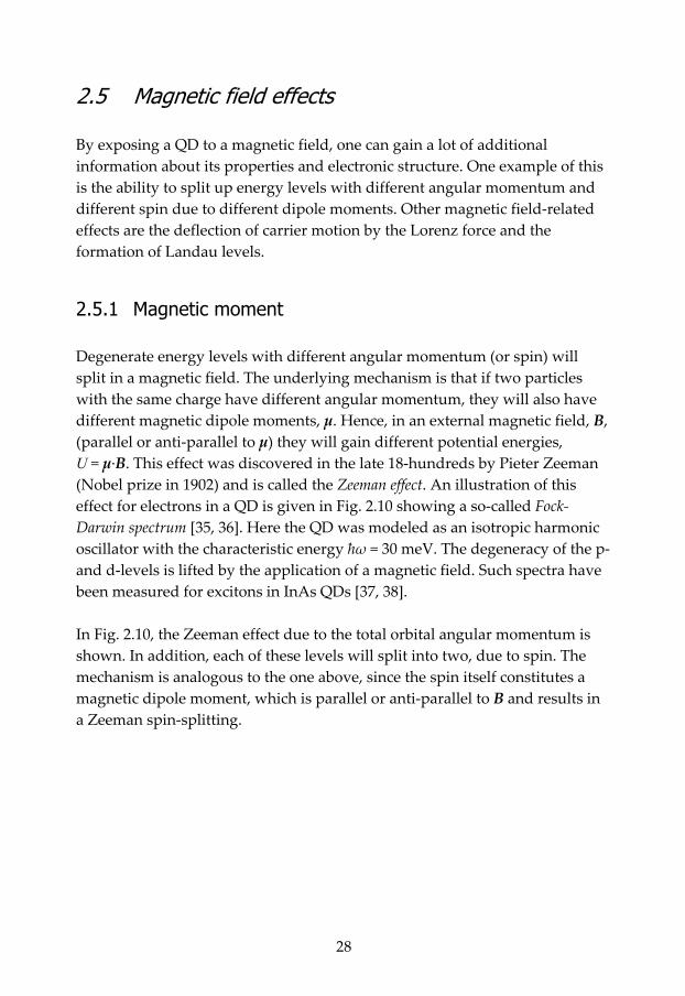
2.5 Magnetic field effects By exposing a QD to a magnetic field, one can gain a lot of additional information about its properties and electronic structure. One example of this is the ability to split up energy levels with different angular momentum and different spin due to different dipole moments. Other magnetic field-related effects are the deflection of carrier motion by the Lorenz force and the formation of Landau levels.
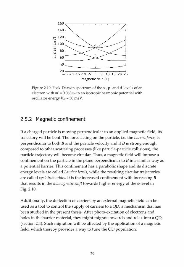
2.5.1 Magnetic moment Degenerate energy levels with different angular momentum (or spin) will split in a magnetic field. The underlying mechanism is that if two particles with the same charge have different angular momentum, they will also have different magnetic dipole moments, µ. Hence, in an external magnetic field, B, (parallel or anti-parallel to µ) they will gain different potential energies, U = µ·B. This effect was discovered in the late 18-hundreds by Pieter Zeeman (Nobel prize in 1902) and is called the Zeeman effect. An illustration of this effect for electrons in a QD is given in Fig. 2.10 showing a so-called Fock-Darwin spectrum [35, 36]. Here the QD was modeled as an isotropic harmonic oscillator with the characteristic energy ħω = 30 meV. The degeneracy of the p- and d-levels is lifted by the application of a magnetic field. Such spectra have been measured for excitons in InAs QDs [37, 38]. In Fig. 2.10, the Zeeman effect due to the total orbital angular momentum is shown. In addition, each of these levels will split into two, due to spin. The mechanism is analogous to the one above, since the spin itself constitutes a magnetic dipole moment, which is parallel or anti-parallel to B and results in a Zeeman spin-splitting.
29
Figure 2.10. Fock-Darwin spectrum of the s-, p- and d-levels of an electron with m* = 0.063m0 in an isotropic harmonic potential with oscillator energy ħω = 30 meV.
2.5.2 Magnetic confinement If a charged particle is moving perpendicular to an applied magnetic field, its trajectory will be bent. The force acting on the particle, i.e. the Lorenz force, is perpendicular to both B and the particle velocity and if B is strong enough compared to other scattering processes (like particle-particle collisions), the particle trajectory will become circular. Thus, a magnetic field will impose a confinement on the particle in the plane perpendicular to B in a similar way as a potential barrier. This confinement has a parabolic shape and its discrete energy levels are called Landau levels, while the resulting circular trajectories are called cyclotron orbits. It is the increased confinement with increasing B that results in the diamagnetic shift towards higher energy of the s-level in Fig. 2.10. Additionally, the deflection of carriers by an external magnetic field can be used as a tool to control the supply of carriers to a QD, a mechanism that has been studied in the present thesis. After photo-excitation of electrons and holes in the barrier material, they might migrate towards and relax into a QD, (section 2.4). Such migration will be affected by the application of a magnetic field, which thereby provides a way to tune the QD population.

30
2.6 Applications of quantum dots There are a number of areas, where it has been predicted that implementation of QDs should result in improved device performances. One example is the QD laser [39] that ideally should be insensitive to temperature variations if the separation distance between QD levels is larger than the thermal energy. QD lasers with promising performance have also been fabricated [40]. The QD infrared photodetector (QDIP) is supposed to have good detector characteristics, since the discreteness of the energy states should result in a decreased dark current. Secondly, for intraband transitions in a QDIP, light can be absorbed at any angle of incidence, while a corresponding QW based detector (QWIP) only can absorb light polarized along the QW confinement direction [41]. A further step in developing QD based detectors is to embed them in a QW structure, so-called dots-in-a-well photodetectors (DWELL). The detector intraband transitions are then between QD and QW states, which allows higher flexibility in device tuning [42]. Other interesting QD-based devices are emitters of entangled photon-pairs and single photon emitters, which are central components in the development of quantum cryptography and quantum information applications. Entangled photon emission from QDs has been demonstrated in the frame of the emission cascade of 2X under the criterion that the two polarization states of X0 are “sufficiently degenerate” [43, 44]. Single photon emission from QDs was first shown using structures, where the QD was embedded in a microcavity in resonance with the QD X0-transition [45]. Subsequently, single photon emission has been achieved by resonant excitation into QD excited states [46, 47], allowing spin-state preparation. Notably, all the studies referred to above were done in the InGaAs materials system.

31
3 Photoluminescence
3.1 Conventional photoluminescence A material, which has been electronically excited, can release energy by light emission and such light is named luminescence. There are several types of luminescence which are categorized depending of the process of excitation that precedes the luminescence. A few examples are; electroluminescence - where the emission results from a current passing through the material, cathodoluminescence - where the emission results from excitation with an electron-beam, and photoluminescence - where the emission results from excitation by light, i.e. photons. Photoluminescence (PL) spectroscopy and the high spatial resolution version of it, called micro-photoluminescence (µPL) spectroscopy, are the main experimental techniques employed in this thesis. The excitation source in most PL experiments is a laser. Some advantages by using laser light are that its wavelength (i.e. the photon energy) is well defined and that the light intensity can be controlled and varied in a very wide range. The basic idea behind the PL experiment is sketched in Fig. 3.1; Photons, with an energy larger than the band gap of the material, Eexc > Eg is absorbed by exciting electrons from the valence band to the conduction band, creating holes in the valence band. These carriers will rapidly relax to the edge of their respective band, by phonon emission or by carrier-carrier interactions like Auger-processes (section 1.2.3), and recombine from there. The energy of the emitted photon, Elum, is a characteristic parameter of the material and can be used to evaluate the band gap width and the existence of various impurities etc. (see sections 1.2.1-1.2.2).

32
Figure 3.1. Illustration of a photoluminescence experiment. a) A photon excites an electron-hole pair in the material. b) The carriers relax to the band edge. c) A photon is emitted by recombination of the electron-hole pair.
In conventional PL experiments on QD structures (Fig. 3.2), the excitation photons are absorbed by creating electron-hole pairs in the barrier material. These carriers will relax to the QD ground state and recombine from there. Thus, the energy of the emitted photon, Elum, is a direct measure of the QD exciton energy and by varying the excitation conditions, one can tune the population and the charge state of the QD (see section 2.2).
Figure 3.2. Illustration of photoluminescence of a QD. A photon excites an electron-hole pair in the barrier, which relax to the QD where they recombine.

33
In conventional PL spectroscopy of QDs, the laser excitation is focused onto the sample by a regular lens, whereby the diameter of the excited area is in the order of ~ 100 µm. For the QD samples studied in this work, the average QD separation distance is ~ 10 µm in case of self assembled QDs, and ~ 7.5 µm in case of pyramidal QD structures, determined by the etching pattern. Thus, a 100 µm laser spot will excite roughly ~ 100 QDs. Hence, to allow studies of single QDs, one must seek ways to reduce the excited sample area and increase the spatial resolution.
3.2 Micro-photoluminescence The technique to decrease the number of excited QDs is called micro-photoluminescence (µPL), since it allows spatial resolution in the micrometer range. This is achieved by replacing the focusing lens by a microscope objective. A sketch of the µPL-setup used in the present work is shown in Fig. 3.3 and some specifications of the constituent components and technical considerations are given in the following subsections.
Figure 3.3. Illustration of the micro-photoluminescence setup.

34
Lasers The main excitation source used in the present work was a tuneable Ti:Al2O3 (titanium-sapphire) laser pumped by a Nd:YVO4 laser. The output wavelength of the Ti:Al2O3 laser can be tuned in the range 700 - 980 nm. For some experiments, a second laser with emission wavelength 1000 nm was used.
Filters and polarizers Generally, various combinations of filters and polarizers are used in the optical paths of excitation and detection when doing optical spectroscopy. Different measurements require different combinations of neutral density filters and long pass-, short pass- and band pass-filters. Glan-Thompson linear polarizers were used as well as Berek-compensators, set as half-wave or quarter-wave plates. Some fundamental polarization optics is described in section 3.5.
Cryostat All µPL experiments were performed at cryogenic temperatures and there are several reasons for this; The energy level spacing in In(Ga)As QDs is at maximum around 25 - 30 meV, which is of the same order as the thermal energy kB·T at room temperature (here, kB = 8.62·10-5 is the Boltzmann constant and T is temperature). Hence, cooling is needed to prevent thermally assisted inter-level excitations. Secondly, emission peaks will broaden at elevated temperatures, due to interaction with phonons, and at sufficiently high temperatures, such an interaction quenches the luminescence totally. Moreover, the exciton binding energy in InAs (GaAs), see table 1.3, corresponds to the thermal energy at T = 15 K (T = 50 K) so bulk excitons will dissociate at higher temperatures. To achieve cooling, the sample is positioned inside a cryostat and the cooling is provided by a continuous flow of liquid helium (LHe) that cools a metal bar (cold finger) onto which the sample is mounted. The lowest temperature reachable in this system is T ≈ 3.5 K. The cryostat is equipped with a heater and an automatic LHe-flow control, allowing temperature control up to room temperature. The cryostat is mounted on the optical table in conjunction with two mechanical actuators, used to move the entire cryostat, in order to

35
navigate on the sample surface with sub-micrometer precision. Optical access to the sample is achieved through the cryostat windows.
Microscope objective The excitation laser is focused onto the sample by a microscope objective with numerical aperture NA ≈ 0.55. In the Fraunhofer diffraction limit, the smallest achievable spot diameter of a collimated light beam with wavelength λ is given by Eq. 3.1 [48]. Hence, at excitation energy Eexc = 1.693 eV corresponding to λexc = 732 nm, the minimum spot diameter is ~1.6 µm.
NAd λ⋅= 22.1 (Eq. 3.1)
The luminescence is also collected through the same microscope objective before it is mirrored into the monochromator and detector.
Camera To navigate on the sample surface and to control the optical alignment of the setup, a video camera is used. A lamp illuminates the sample with white light, when a visual image is needed and the video camera, connected to a monitor, provides an image of the sample surface and the diffraction pattern of the focused laser spot.
Monochromator and detector The luminescence signal is dispersed by a single grating monochromator with length 0.55 m. The grating has 1200 grooves/mm and is blazed for 750 nm. The detector used in the present work is a Si-CCD, cooled with liquid nitrogen. The best spectral resolution achievable has been determined to be 0.075 meV at 1.35 eV. For some measurements, where higher spectral resolution was needed, the Si-CCD was mounted on single grating monochromator with a length of 1.5 m. The best spectral resolution achievable in that case was ~ 0.025 meV.

36
3.3 Photoluminescence excitation Due to the rapid relaxation of carriers in a QD, the luminescence seen at moderate excitation intensities originates from recombinations in the QD ground state. By increasing the excitation intensity, excited states can also be populated due to state filling, but this is only after the ground state is filled. At such high carrier population, and depending on the exact population at the instant of carrier recombination, the luminescence energy will vary significantly due to Coulomb- and exchange-interactions between the carriers in the QD. Therefore, to be able to probe the QD excited states, one turns to photoluminescence excitation (PLE) measurements. The principle of a PLE experiment is shown in Fig. 3.4. The excitation energy is swept, illustrated by the varying arrow length in Fig. 3.4(a), while the detection energy is fixed, so a specific recombination process in monitored. In Fig. 3.4(a) – (b) the QD ground state-transition is monitored, while the excitation is swept in the range of the excited QD states. At a certain excitation energy, the QD is excited resonantly, resulting in an increased recombination rate in the monitored transition, Fig. 3.4(b). A PLE measurement resembles an absorption measurement but with the important difference that it requires carriers to relax (or by some mechanism transfer) to the state that is monitored and it is therefore more selective.
Figure 3.4. A photoluminescence excitation experiment. (a) The excitation energy is varied, while the ground state emission is monitored. In (b), the excitation is resonant with an excited QD state, resulting in increased intensity of the monitored emission.

37
3.4 Magneto-photoluminescence To exert the QD samples to an external magnetic field, the cryostat is inserted into the bore of a superconducting solenoid magnet. To achieve super-conductivity, the solenoid is immersed in LHe. The maximum field strength available in the µPL-setup is B = 5 T. The direction of the magnetic field with respect to the cryostat is fixed and readily allows studies in Faraday geometry, i.e. with the magnetic field applied parallel to the optical axis (B∥z), see Fig. 3.5(a). However, by mounting the sample together with a mirror inside the cryostat, the magnetic field could also be applied perpendicular to the optical axis (B⊥z), i.e. in Voigt geometry, Fig. 3.5(b). The physical significance of the difference between these geometries is based on the fact that the z-axis is the direction onto which the spin projection of carriers is measured. It is also the direction onto which the spin projection of carriers can be polarized and onto which the nuclear spins are polarized. Therefore, applying B∥z will act to preserve the spin polarization, whereas applying B⊥z, will spoil the spin preservation (the Hanle effect) [8, 9].
Figure 3.5. Illustration of a magnetic field applied in (a) Faraday geometry and (b) Voigt geometry.
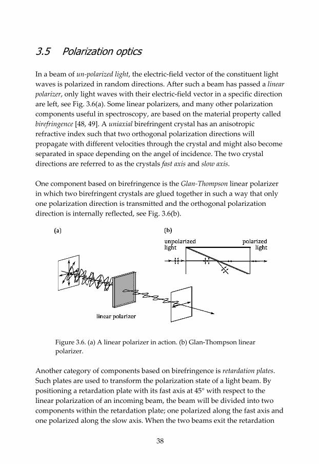
38
3.5 Polarization optics In a beam of un-polarized light, the electric-field vector of the constituent light waves is polarized in random directions. After such a beam has passed a linear polarizer, only light waves with their electric-field vector in a specific direction are left, see Fig. 3.6(a). Some linear polarizers, and many other polarization components useful in spectroscopy, are based on the material property called birefringence [48, 49]. A uniaxial birefringent crystal has an anisotropic refractive index such that two orthogonal polarization directions will propagate with different velocities through the crystal and might also become separated in space depending on the angel of incidence. The two crystal directions are referred to as the crystals fast axis and slow axis. One component based on birefringence is the Glan-Thompson linear polarizer in which two birefringent crystals are glued together in such a way that only one polarization direction is transmitted and the orthogonal polarization direction is internally reflected, see Fig. 3.6(b).
Figure 3.6. (a) A linear polarizer in action. (b) Glan-Thompson linear polarizer.
Another category of components based on birefringence is retardation plates. Such plates are used to transform the polarization state of a light beam. By positioning a retardation plate with its fast axis at 45° with respect to the linear polarization of an incoming beam, the beam will be divided into two components within the retardation plate; one polarized along the fast axis and one polarized along the slow axis. When the two beams exit the retardation

39
plate, their respective phases have been shifted due to the different velocities for the two polarizations. The introduced phase shift is denoted the retardance. If the retardance corresponds to half a wavelength of the light, the component is a half-wave plate and if the retardance corresponds to a quarter of the wavelength, the component is a quarter-wave plate. A half-wave plate, with its fast axis at 45° with respect to the impinging linear polarization, rotates the incoming linear polarization direction by 90°, Fig. 3.7(a). A quarter-wave plate at 45° transforms a linearly polarized beam into a circularly polarized one, see Fig. 3.7(b), as well as it transforms a circularly polarized beam into a linearly polarized one.
Figure 3.7. (a) A half-wave plate rotates the linear polarization by 90°. (b) A quarter-wave plate transforms linear polarization into circular polarization.

40

41
4 Summary of the papers
Papers 1 - 3 are devoted to the ability to control the charge state of individual self-assembled QDs by an applied external magnetic field. The mechanism behind this charge control is attributed to a modulation in the carrier transport dynamics in the WL during migration towards a QD, due to a magnetic field induced decrease of the carriers drift velocity. Since this effect has a very different strength for electrons and holes, it is seen as a charge state redistribution in single QD studies, whereas in studies of ensembles of QDs, it is seen as a decrease in the QD luminescence intensity without a corresponding increase of the WL luminescence intensity. The suggested model is further tested by applying a second infra-red photo-excitation, which has earlier been shown to decrease the local electric field around QDs and by investigating the temperature dependence of the effect. In papers 4 - 6 a means to spin polarize the neutral exciton (X0) in self-assembled QDs is explored. Although X0 is known to have a poor spin preservation due to the anisotropic electron – hole exchange interaction (AEI), it is shown that its spin can indeed be polarized. This is achieved by by-passing the AEI in a small time window during which an electron is alone in the QD. The possibility to reach such a scenario is opened up since electrons are captured faster than holes into QDs, after photo-excitation with the proper energy. The dependence of this effect on excitation energy and QD density is studied. A sole electron in a QD can transfer its spin to the nuclei and, as a result, a nuclear magnetic field (~ 1.5 T) is built up. The time to build up this field was measured to be ~ 10 ms. This field will stabilize the X0 spin in a similar manner as an external magnetic field would, resulting in a polarization degree of ~ 60 % for X0. In paper 7, pyramidal QD structures are studied to unveil shake-up (SU) processes in single QDs. The studied process is SU of a hole at the

42
recombination of the positively charged exciton (X+). After recombination of X+, the QD is normally populated with a hole in the ground state, but in the SU process some of the recombination energy is instead transferred to the hole so that it afterwards occupies an excited state instead. This process is detected experimentally as a luminescence peak at lower energy and with an intensity about 1000 times lower than the X+ peak intensity. Thus, studies of these processes require very high light extraction efficiency, which is the reason why pyramidal QD structures were used. The attribution of the detected satellite peak to a SU process is based on its intensity correlation with the X+ peak, photoluminescence excitation measurements, magnetic field measurements and numerical computations.

43
Bibliography
[1] K. W. Böer, Survey of Semiconductor Physics, 2nd ed., (John Wiley & Sons, 2002). [2] S. Sze, Physics of Semiconductor Devices, 3rd ed., (John Wiley & Sons, 2007). [3] J. H. Davies, The Physics of Low-Dimensional Semiconductors, (Cambridge University Press, 1998). [4] J. R. Chelikowsky and M. L. Cohen, Phys. Rev. B 14, 556 (1976). [5] I. Vurgaftman, J. R. Meyer and L. R. Ram-Mohan, J. Appl. Phys., 89, 5815. (2001). [6] S. Adachi, J. Appl. Phys. 58, R1 (1985). [7] E. S. Moskalenko, K. F. Karlsson, P. O. Holtz, B. Monemar, W. V. Schoenfeld, J. M. Garcia and P. M. Petroff, Phys. Rev. B 66, 195332 (2002). [8] M. I. Dyakonov (ed.), Spin physics in semiconductors (Springer series in solid-state sciences, vol. 157), (Springer, 2008). [9] F. Meier and B. P. Zakharchenya (ed.), Optical orientation (Modern Problems in Condensed Matter Sciences, vol. 8), (North Holland Physics Publ., 1984). [10] K. S. Krane, Introductory nuclear physics, (John Wiley & Sons, 1988). [11] L. Jacak, P. Hawrylak and A. Wójs, Quantum dots, (Springer, 1998). [12] Z. I. Alferov, V. M. Andreev, V. I. Korolkov, E. L. Portnoi and D. N. Tretyakov, Sov, Phys.-Semicond. 2, 1289 (1969).

44
[13] I. Hayashi, M. B. Panish, P. W. Foy and S. Sumski, Appl. Phys. Lett. 17, 109 (1970). [14] R. Dingle, W Wiegmann and C. H. Henry, Phys. Rev. Lett. 33, 827 (1974). [15] S. Raymond, S. Fafard, P. J. Poole, A. Wojs, P. Hawrylak, and S. Charbonneau, Phys. Rev. B 54, 11548 (1996). [16] J. Johansen, B. Julsgaard, S. Stobbe, J. M. Hvam, and P. Lodahl, Phys. Rev. B 81, 081304(R) (2010). [17] A. Hartmann, Y. Ducommun, E. Kapon, U. Hohenester and E. Molinari, Phys. Rev. B 84, 5648 (2000). [18] A. Hartmann, Y. Ducommun, M. Bächthold and E. Kapon, Physica E 7, 461 (2000). [19] E. S. Moskalenko, K. F. Karlsson, P. O. Holtz, B. Monemar, W. V. Schoenfeld, J. M. Garcia, and P. M. Petroff, Phys. Rev. B 64, 085302 (2001). [20] E. S. Moskalenko, V. Donchev, K. F. Karlsson, P. O. Holtz, B. Monemar, W. V. Schoenfeld, J. M. Garcia and P. M. Petroff, Phys. Rev. B 68, 155317 (2003). [21] R. Heitz, T. R. Ramachandran, A. Kalburge, Q. Xie, I. Mukhametzhanov, P. Chen, and A. Madhukar, Phys. Rev. Lett. 78, 4071 (1997). [22] J. M. García, T. Mankad, P. O. Holtz, P. J. Wellman and P. M. Petroff, Appl. Phys. Lett. 72, 3172 (1998). [23] J. M. García, G. Medeiros-Ribeiro, K. Schmidt, T. Ngo, J. L. Feng, A. Lorke, J. Kotthaus and P. M. Petroff, Appl. Phys. Lett. 71, 2014 (1997). [24] A. Hartmann, Y. Ducommun, K. Leifer and E. Kapon, J. Phys. Cond. Matter 11, 5901 (1999). [25] M. H. Baier, E. Pelucchi, E. Kapon, S. Varoutsis, M. Gallart, I. Robert-Philip and I. Abram, Appl. Phys. Lett. 84, 648 (2004).

45
[26] M. H. Baier, C. Constantin, E. Pelucchi and E. Kapon, Appl. Phys. Lett. 84, 1967 (2004). [27] G. Biasiol, A. Gustafsson, K. Leifer and E. Kapon, Phys. Rev. B 65, 205306 (2002). [28] E. Pelucchi, S. Watanabe, K. Leifer, Q. Zhu, B. Dwir, P. D. L. Rios and E. Kapon, Nano Lett. 7, 1282 (2007). [29] Q. Zhu, E. Pelucchi, S. Dalessi, K. Leifer, M.-A. Dupertuis and E. Kapon, Nano Lett. 6, 1036 (2006). [30] L. O. Mereni, V. Dimastrodonato, R. J. Young and E. Pelucchi, Appl. Phys. Lett. 94, 223121 (2009). [31] V. Dimastrodonato, L. O. Mereni, R. J. Young and E. Pelucchi, Phys. Status Solidi B 247, 1862 (2010). [32] E. Pelucchi, N. Moret, B. Dwir, D. Y. Oberli, A. Rudra, N. Gogneau, A. Kumar, E. Kapon, E. Levy and A. Palevski, J. Appl. Phys. 99, 093515 (2006). [33] E. S. Moskalenko, M. Larsson, W. V. Schoenfeld, P. M. Petroff and P. O. Holtz, Phys. Rev. B 73, 155336 (2006). [34] E. S. Moskalenko, M. Larsson, K. F. Karlsson, P. O. Holtz, B. Monemar, W. V. Schoenfeld and P. M. Petroff, Nano Lett. 7, 188 (2007). [35] V. Fock, Z. Phys. 47, 446 (1928). [36] T. Tanaka, Y. Arakawa and G. W. E. Bauer, Phys. Rev. B 50, 7719 (1994). [37] S. Raymond, S. Studenikin, A. Sachrajda, Z.Wasilewski, S. J. Cheng, W. Sheng, P. Hawrylak, A. Babinski, M. Potemski, G. Ortner and M. Bayer, Phys. Rev. Lett. 92, 187402 (1994). [38] S. Awirothananon, S. Raymond, S. Studenikin, M. Vachon, W. Render, A. Sachrajda, X. Wu, A. Babinski, M. Potemski, S. Fafard, S. J. Cheng, M. Korkusinski and P. Hawrylak, Phys. Rev. B 78, 235313 (2008). [39] Y. Arakawa and H. Sakaki, Appl. Phys. Lett. 40, 939 (1982).

46
[40] K. Otsubo, N. Hatori, M. Ishida, S. Okumura, T. Akiyama, Y. Nakata, H. Ebe, M. Sugawara and Y. Arakawa, Jap. J. App. Phys. 43, L1124 (2004). [41] J. Phillips, K. Kamath, and P. Bhattacharya, Appl. Phys. Lett. 72, 2020 (1998). [42] L. Höglund, C. Asplund, Q. Wang, S. Almqvist, H. Malm, E. Petrini, J. Y. Andersson, P. O. Holtz, H. Pettersson, Appl. Phys. Lett. 88, 213510 (2006). [43] R. M. Stevenson, R. J. Young, P. Atkinson, K. Cooper, D. A. Ritchie and A. J. Shields, Nature 439, 179 (2006). [44] N. Akopian, N. H. Lindner, E. Poem, Y. Berlatzky, J. Avron, D. Gershoni, B. D. Gerardot and P. M. Petroff, Phys. Rev. Lett. 96, 130501 (2006). [45] P. Michler, A. Kiraz, C. Becher, W. V. Schoenfeld, P. M. Petroff, Lidong Zhang, E. Hu and A. Imamogùlu, Science 290 2282 (2000). [46] A. Zrenner, E. Beham, S. Stufler, F. Findeis, M. Bichler and & G. Abstreiter, Nature 418, 612 (2002). [47] P. Ester, L. Lackmann, S. Michaelis de Vasconcellos, M. C. Hübner, A. Zrenner and M. Bichler, Appl. Phys. Lett. 91, 111110 (2007) [48] Fundamental optics, as of January 2011 provided by CVI Melles Griot at www.cvimellesgriot.com/products/Documents/TechnicalGuide/fundamental-Optics.pdf. [49] E. Hecht, Optics, 4th ed., (Addison Wesley, 2002).

47
Index
A
artificial atoms ........................................20 Auger process..........................................12
B
band gap................................................2, 7 band index.................................................7 band structure...........................................7 bi-exciton.................................................22 birefringence ...........................................38 Bloch’s theorem.........................................7 body centered cubic ...................................5 Bohr model ................................................1 Bound exciton .........................................12 bright excitons ........................................21 Brillouin zone............................................5
C
carriers ......................................................3 cathodoluminescence...............................31 circularly polarized ...........................15, 39 cold finger ...............................................34 collection area..........................................27 conduction band........................................2 critical thickness......................................24 Cryostat...................................................34 crystal momentum ....................................7
D
dark excitons ...........................................21 density of states.......................................18
diamagnetic shift.....................................29 diamond lattice .........................................4 direct band gap .......................................10 donor-acceptor-pair.................................12 dots-in-a-well photodetectors..................30
E
effective mass approach.............................8 electroluminescence ................................31 entangled photon-pairs ...........................30 envelope function approximation .............8 exciton.....................................................10
F
face centered cubic ....................................3 Faraday geometry ...................................37 fast axis ...................................................38 fermion......................................................2 Fock-Darwin spectrum...........................28 Free-to-bound..........................................11
G
Glan-Thompson ......................................38
H
half-wave plate ........................................39 Hanle effect .............................................37 heterostructure........................................17 hole............................................................3 hyperfine interaction...............................14

48
I
indirect band gap ....................................10 insulator....................................................2
K
Knight field .............................................15 k-space.......................................................5
L
linear polarizer ........................................38 Lorenz force.............................................29 Luminescence ..........................................31
M
metal..........................................................2 micro-photoluminescence..................31, 33 Monochromator ......................................35
N
negatively charged exciton......................22 neutral exciton ........................................21 nuclear spin.............................................14 nucleons ..................................................14
O
Overhauser field......................................15
P
particle in a box.......................................19 Pauli exclusion principle ..........................2 photoluminescence ..................................31 photoluminescence excitation .................36 polarized light .........................................38 positively charged exciton.......................22
Q
QD infrared photodetector......................30 QD laser..................................................30 quantum confinement.............................18 quantum dot............................................18 quantum structure..................................18 quantum well ..........................................18 quantum wire..........................................18
quarter-wave plate ..................................39
R
reduced mass...........................................11 reduced zone scheme .................................7 retardance ...............................................39 retardation plates ....................................38 right handed polarization .......................15
S
satellite spectroscopy ..............................13 satellite-peak ...........................................13 satellite-process.......................................13 self-assembled..........................................24 semiconductor...........................................2 shake-up process .....................................13 single photon emitters ............................30 slow axis .................................................38 spin-orbit coupling ...................................9 spin-polarized electrons ..........................15 state filling........................................23, 36 Stranski-Krastanow growth ...................24
T
the lattice constant....................................3 titanium-sapphire ...................................34
U
uniaxial ...................................................38 un-polarized light ...................................38
V
valence band..............................................2 Voigt geometry........................................37
W
wave function leakage.............................19 wetting layer...........................................24 WL localizing potential ..........................27
Z
Zeeman effect ..........................................28 zinc-blend structure .................................3