Optical network technologies for HPC: computer-architects ...
14
Optical network technologies for HPC: computer-architects point of view Michihiro Koibuchi 1a) , Ikki Fujiwara 1 , Kiyo Ishii 2 , Shu Namiki 2 , Fabien Chaix 3 , Hiroki Matsutani 4 , Hideharu Amano 4 , and Tomohiro Kudoh 5 1 National Institute of Informatics, 2–1–2 Hitotsubashi, Chiyoda-ku, Tokyo 101–8430, Japan 2 National Institute of Advanced Industrial Science and Technology, 1–1–1 Umezono, Tsukuba, Ibaraki 305–8560, Japan 3 CARV Laboratory, FORTH-ICS, Heraklion, Greece 4 Keio University, 3–14 –1 Hiyoshi, Kohoku-ku, Yokohama, Kanagawa 223–8522, Japan 5 Information Technology Center, The University of Tokyo, 2–11–16 Yayoi, Bunkyo-ku, Tokyo 113–8658, Japan a) [email protected] Abstract: Optical network technologies, such as circuit switching, wave- length division multiplex and silicon photonics, have been considered for high-performance computing (HPC) systems to achieve low communication latency, high link bandwidth and low power consumption. However, conven- tional HPC systems still use packet networks with electric switches. Only active optical cables for inter-cabinet long links are borrowed from optical network technologies. This paper firstly reviews the gap between the conven- tional HPC networks and feasible optical network technologies. We explain our pessimism that this gap will continue to exist by the beginning of the post-Moore era, i.e. 2025–2030. It secondly illustrates our research vision that HPC networks will be able to adopt optical circuit switching, possibly using free-space optics in the post-Moore era. Keywords: optical interconnection networks, network topology, high-per- formance computing, free-space optics, circuit switching Classification: Fiber optics, Microwave photonics, Optical interconnec- tion, Photonic signal processing, Photonic integration and systems References [1] K. S. Hemmert, J. S. Vetter, K. Bergman, C. Das, A. Emami, C. Janssen, D. K. Panda, C. Stunkel, K. Underwood and S. Yalamanchili: Report on Institute for Advanced Architectures and Algorithms, Interconnection Networks Workshop (2008) http://ft.ornl.gov/doku/_media/iaaicw/iaa-ic-2008-workshop-report-v09. pdf. [2] B. Towles, J. P. Grossman, B. Greskamp and D. E. Shaw: ISCA (2014) 1. DOI:10.1109/ISCA.2014.6853238 © IEICE 2016 DOI: 10.1587/elex.13.20152007 Received December 20, 2015 Accepted January 20, 2016 Published March 25, 2016 1 REVIEW PAPER IEICE Electronics Express, Vol.13, No.6, 1–14
Transcript of Optical network technologies for HPC: computer-architects ...

Optical network technologiesfor HPC: computer-architectspoint of view
Michihiro Koibuchi1a), Ikki Fujiwara1, Kiyo Ishii2,Shu Namiki2, Fabien Chaix3, Hiroki Matsutani4,Hideharu Amano4, and Tomohiro Kudoh51 National Institute of Informatics,
2–1–2 Hitotsubashi, Chiyoda-ku, Tokyo 101–8430, Japan2 National Institute of Advanced Industrial Science and Technology,
1–1–1 Umezono, Tsukuba, Ibaraki 305–8560, Japan3 CARV Laboratory, FORTH-ICS, Heraklion, Greece4 Keio University,
3–14–1 Hiyoshi, Kohoku-ku, Yokohama, Kanagawa 223–8522, Japan5 Information Technology Center, The University of Tokyo,
2–11–16 Yayoi, Bunkyo-ku, Tokyo 113–8658, Japan
Abstract: Optical network technologies, such as circuit switching, wave-
length division multiplex and silicon photonics, have been considered for
high-performance computing (HPC) systems to achieve low communication
latency, high link bandwidth and low power consumption. However, conven-
tional HPC systems still use packet networks with electric switches. Only
active optical cables for inter-cabinet long links are borrowed from optical
network technologies. This paper firstly reviews the gap between the conven-
tional HPC networks and feasible optical network technologies. We explain
our pessimism that this gap will continue to exist by the beginning of the
post-Moore era, i.e. 2025–2030. It secondly illustrates our research vision
that HPC networks will be able to adopt optical circuit switching, possibly
using free-space optics in the post-Moore era.
Keywords: optical interconnection networks, network topology, high-per-
formance computing, free-space optics, circuit switching
Classification: Fiber optics, Microwave photonics, Optical interconnec-
tion, Photonic signal processing, Photonic integration and systems
References
[1] K. S. Hemmert, J. S. Vetter, K. Bergman, C. Das, A. Emami, C. Janssen, D. K.Panda, C. Stunkel, K. Underwood and S. Yalamanchili: Report on Institute forAdvanced Architectures and Algorithms, Interconnection Networks Workshop(2008) http://ft.ornl.gov/doku/_media/iaaicw/iaa-ic-2008-workshop-report-v09.pdf.
[2] B. Towles, J. P. Grossman, B. Greskamp and D. E. Shaw: ISCA (2014) 1.DOI:10.1109/ISCA.2014.6853238
© IEICE 2016DOI: 10.1587/elex.13.20152007Received December 20, 2015Accepted January 20, 2016Published March 25, 2016
1
REVIEW PAPER IEICE Electronics Express, Vol.13, No.6, 1–14

[3] N. Tanabe, J. Yamamoto, H. Nishi, T. Kudoh, Y. Hamada, H. Nakajo and H.Amano: Cluster Comput. 5 [1] (2002) 7. DOI:10.1023/A:1012732403321
[4] P. Kogge and J. Shalf: Comput. Sci. Eng. 15 [6] (2013) 16. DOI:10.1109/MCSE.2013.95
[5] The NAS Parallel Benchmarks. http://www.nas.nasa.gov/Software/NPB/.[6] Top 500 Sites. http://www.graph500.org/.[7] SimGrid: Versatile Simulation of Distributed Systems. http://simgrid.gforge.
inria.fr/.[8] F. Chaix, I. Fujiwara and M. Koibuchi: Euromicro International Conference on
Parallel, Distributed, and Network-Based Processing(PDP) (2016).[9] M. Koibuchi, H. Matsutani, H. Amano, D. F. Hsu and H. Casanova: ISCA
(2012) 177. DOI:10.1109/ISCA.2012.6237016[10] H. Casanova, A. Giersch, A. Legrand, M. Quinson and F. Suter: J. Parallel
Distrib. Comput. 74 (2014) 2899. DOI:10.1016/j.jpdc.2014.06.008[11] J. Kim, W. J. Dally, S. Scott and D. Abts: ISCA (2008) 77. DOI:10.1109/ISCA.
2008.19[12] A. Singla, C.-Y. Hong, L. Popa and P. B. Godfrey: NSDI (2012) 225.[13] M. Besta and T. Hoefler: SC (2014) 348. DOI:10.1109/SC.2014.34[14] Combinatorics Wiki. The Degree Diameter Problem for General Graphs.
http://combinatoricswiki.org/wiki/The_Degree_Diameter_Problem_for_General_Graphs.
[15] GraphGolf: The Order/degree Problem Competition. http://research.nii.ac.jp/graphgolf/.
[16] J. Flich, T. Skeie, A. Mejia, O. Lysne, P. Lopez, A. Robles, J. Duato, M.Koibuchi, T. Rokicki and J. C. Sancho: IEEE Trans. Parallel Distrib. Syst. 23(2012) 405. DOI:10.1109/TPDS.2011.190
[17] M. Koibuchi, I. Fujiwara, H. Matsutani and H. Casanova: HPCA (2013) 484.DOI:10.1109/HPCA.2013.6522343
[18] W. D. Dally and B. Towles: Principles and Practices of InterconnectionNetworks (Morgan Kaufmann, 2003).
[19] T. Kudoh, H. Nishi, J. Yamamoto, R. Ueno, K. Harasawa, S. Fukuda, Y.Shikichi, S. Akutsu, K. Tasho and H. Amano: Hot Interconnects 9 (2001) 119.DOI:10.1109/HIS.2001.946703
[20] S. Scott, D. Abts, J. Kim and W. J. Dally: ISCA (2006) 16. DOI:10.1109/ISCA.2006.40
[21] K. J. Barker, A. F. Benner, R. R. Hoare, A. Hoisie, A. K. Jones, D. J. Kerbyson,D. Li, R. G. Melhem, R. Rajamony, E. Schenfeld, S. Shao, C. B. Stunkel and P.Walker: SC (2005). DOI:10.1109/SC.2005.48
[22] K. Kanonakis, Y. Yin, P. N. Ji and T. Wang: OFC (2015) Th4G.7. DOI:10.1364/OFC.2015.Th4G.7
[23] K. Christodoulopoulos, K. Katrinis, M. Russini and D. O. Mahony: OFC(2014) Th2A.11. DOI:10.1364/OFC.2014.Th2A.11
[24] G. Porter, R. D. Strong, N. Farrington, A. Forencich, P. Chen-Sun, T. Rosing,Y. Fainman, G. Papen and A. Vahdat: SIGCOMM (2013) 447. DOI:10.1145/2534169.2486007
[25] Z. Zhu and S. Zhong: OFC (2014) Th2A.60. DOI:10.1364/OFC.2014.Th2A.60[26] P. Samadi, J. Xu and K. Bergman: OFC (2015) Th4G.6. DOI:10.1364/OFC.
2015.Th4G.6[27] Y. Pointurie, B. Uscumlic, M. A. Mestre, P. Jenneve, H. Mardoyan, A. Dupas
and S. Bingo: ECOC (2015) Tu.3.6.4. DOI:10.1109/ECOC.2015.7341959[28] G. M. Saridis, E. Hugues-Salas, Y. Yan, S. Yan, S. Poole, G. Zervas and D.
Siomenidou: OFC (2015) W1D.2. DOI:10.1364/OFC.2015.W1D.2[29] R. Proietti, Z. Cao, Y. Li and S. J. B. Yoo: OFC (2014) Th2A.59. DOI:10.1364/
OFC.2014.Th2A.59
© IEICE 2016DOI: 10.1587/elex.13.20152007Received December 20, 2015Accepted January 20, 2016Published March 25, 2016
2
IEICE Electronics Express, Vol.13, No.6, 1–14

[30] W. Miao, F. Agraz, H. de Waardt, S. Spadaro, H. J. S. Dorren and N.Calabretta: OFC (2015) Th2A.66. DOI:10.1364/OFC.2015.Th2A.66
[31] R. Takahashi, S. Ibrahim, T. Segawa, T. Nakahara, H. Ishikawa, Y. Suzaki, Y.Huang, K. Kitayama and A. Hiramatsu: OFC (2015) W3D.4. DOI:10.1364/OFC.2015.W3D.4
[32] J. Kim, W. J. Dally and D. Abts: ISCA (2007) 126. DOI:10.1145/1273440.1250679
[33] J. Mudigonda, P. Yalagandula and J. C. Mogul: USENIX ATC (2011) 1.[34] W. J. Dally: IAA Workshop (2008).[35] Product guide, Finisar. https://www.finisar.com/roadms-wavelength-management/
10wsaaxxfll.[36] K. Tanizawa, K. Suzuki, M. Toyama, M. Ohtsuka, N. Yokoyama, K.
Matsumaro, M. Seki, K. Koshino, T. Sugaya, S. Suda, G. Cong, T. Kimura,K. Ikeda, S. Namiki and H. Kawashima: Opt. Express 13 (2015) 17599.DOI:10.1364/OE.23.017599
[37] J. Boyd: IEEE Spectrum 52 [6] (2015) 20. DOI:10.1109/MSPEC.2015.7115550
[38] I. Fujiwara, M. Koibuchi, T. Ozaki, H. Matsutani and H. Casanova: HPCA(2015) 390. DOI:10.1109/HPCA.2015.7056049
[39] Earth simulator project. http://www.jamstec.go.jp/es/en/index.html.[40] Y. Ajima, S. Sumimoto and T. Shimizu: Computer 42 (2009) 36. DOI:10.1109/
MC.2009.370[41] N. Hamedazimi, Z. Qazi, H. Gupta, V. Sekar, S. R. Das, J. P. Longtin, S.
Himanshu and T. Ashish: Proc. of the ACM Conference on SIGCOMM (2014)319. DOI:10.1145/2619239.2626328
[42] A Draft APT Report on Direct Single-Mode-Fiber Coupled Free-Space OpticalCommunications to Expand the Flexibility in Fiber-Based Services. Asia-Pacific Telecommunity, APT Standardization Program Forum (2013).
1 Introduction
High-performance computing (HPC) systems historically use a switch-based packet
network. Their unique requirement is low communication latency, e.g., 1 µs
communication latency across the system [1] when compared to a local area
network (LAN). The switch delay to forward a message becomes dozens or
hundreds of nanoseconds, such as 45.3 ns on BlueGene/Q, 40.1 ns on Anton-2
[2] and about 100 ns even in commodity InfiniBand QDR switches. The receiving
and sending overhead at a host could be small, e.g. 100 ns, by enabling intelligent
network interfaces [3, 4]. As device technology and its corresponding software
overhead continue to improve, message passing interface (MPI) communication is
expected to become more latency sensitive.
With the current technology, electric switch delays are large compared to the
link delays. To achieve low latency, a topology of switches should thus have low
diameter and low average shortest path length (ASPL), both measured in numbers
of switch hops. This will be an important challenge of the HPC networks.
Link bandwidth is also an important concern and therefore a rule of thumb of a
parallel computer system is sometimes considered as performance measure of the
various hardware components. 1-MIPS (million instructions per second) processor
should have a 1MB of memory and a 1-Mbps network connection in a parallel
© IEICE 2016DOI: 10.1587/elex.13.20152007Received December 20, 2015Accepted January 20, 2016Published March 25, 2016
3
IEICE Electronics Express, Vol.13, No.6, 1–14

computer. A compute node will have 1 TFLOPS (tera floating-point operations per
second) of computation power, thus requiring 1 Tbps of link bandwidth.
In addition to latency and bandwidth, power consumption can be a limiting
factor in designing a supercomputer, such as a limit of 20MW per supercomputer.
In an HPC network power efficiency of data movement would be the bottleneck to
scaling up the system.
Optical technologies have long-term potential for having a great impact on end-
to-end network latency, link bandwidth and power consumption in HPC networks,
and are expected to be able to satisfy the above severe requirements.
In this paper, we review the optical technologies available for HPC systems
from the computer-architect point of view. Specially, we consider (i) why existing
HPC systems use electric switches and (ii) whether the current network architecture
continues in HPC systems.
Beside the end-to-end network latency, link bandwidth and power consump-
tion, the HPC networks have a large number of other requirements for the next-
generation of supercomputers, such as 100M messages/s throughput for MPI
communication, and 1,000M messages/s for load/store communication models
[1]. However, they do not directly relate to the contribution by optical technologies
and their review is out of the scope of this paper.
The rest of this paper is organized as follows. The conventional HPC networks
and trends in their research are described in Section 2. In Section 3 we review the
application of optical technologies to HPC systems. In Section 4, we explain our
pessimism regarding the gap between existing HPC networks and feasible optical
technologies. In Section 5, we consider the future direction for HPC networks that
includes optical circuit switching possibly with free-space optics (FSO). Section 6
concludes our review.
2 Conventional HPC networks using electric switches
2.1 Typical communication patterns
Decades of parallel computing research have gone into developing efficient map-
pings of applications with regular communication patterns onto traditional network
topologies (e.g., numerical linear algebra kernels on a k-ary n-cube topology). By
contrast, a large number of parallel applications and benchmarks that have port-
ability by using the MPI function generate two typical communication patterns: all-
to-all and stencil (neighboring) accesses. For example, the Fourier Transform (FT)
and the Integer Sort (IS) from among the NAS Parallel Benchmarks [5] and the
replicated version of the Graph500 MPI program [6] and Memory Multiplication
(MM) by SimGrid [7] have all-to-all communication accesses. By contrast, the
Block Tridiagonal solver (BT), the Scalar Penta-diagonal solver (SP), the Lower-
Upper Gauss-Seidel solver (LU) and the Himeno benchmark have stencil commu-
nication patterns in our analysis results [8]. The Multi-Grid on a sequence of
meshes (MG) has both long and short-distance data transfers.
Interestingly, for most applications, performance is latency-sensitive according
to our simulation results [8]. We investigate the influences of the switch delay and
the network topology on performance, since both of them affect communication
© IEICE 2016DOI: 10.1587/elex.13.20152007Received December 20, 2015Accepted January 20, 2016Published March 25, 2016
4
IEICE Electronics Express, Vol.13, No.6, 1–14
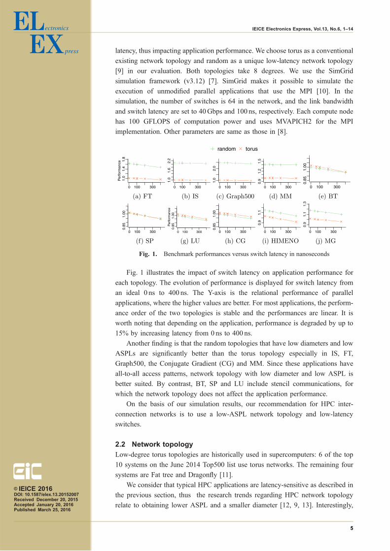
latency, thus impacting application performance. We choose torus as a conventional
existing network topology and random as a unique low-latency network topology
[9] in our evaluation. Both topologies take 8 degrees. We use the SimGrid
simulation framework (v3.12) [7]. SimGrid makes it possible to simulate the
execution of unmodified parallel applications that use the MPI [10]. In the
simulation, the number of switches is 64 in the network, and the link bandwidth
and switch latency are set to 40Gbps and 100 ns, respectively. Each compute node
has 100 GFLOPS of computation power and uses MVAPICH2 for the MPI
implementation. Other parameters are same as those in [8].
Fig. 1 illustrates the impact of switch latency on application performance for
each topology. The evolution of performance is displayed for switch latency from
an ideal 0 ns to 400 ns. The Y-axis is the relational performance of parallel
applications, where the higher values are better. For most applications, the perform-
ance order of the two topologies is stable and the performances are linear. It is
worth noting that depending on the application, performance is degraded by up to
15% by increasing latency from 0 ns to 400 ns.
Another finding is that the random topologies that have low diameters and low
ASPLs are significantly better than the torus topology especially in IS, FT,
Graph500, the Conjugate Gradient (CG) and MM. Since these applications have
all-to-all access patterns, network topology with low diameter and low ASPL is
better suited. By contrast, BT, SP and LU include stencil communications, for
which the network topology does not affect the application performance.
On the basis of our simulation results, our recommendation for HPC inter-
connection networks is to use a low-ASPL network topology and low-latency
switches.
2.2 Network topology
Low-degree torus topologies are historically used in supercomputers: 6 of the top
10 systems on the June 2014 Top500 list use torus networks. The remaining four
systems are Fat tree and Dragonfly [11].
We consider that typical HPC applications are latency-sensitive as described in
the previous section, thus the research trends regarding HPC network topology
relate to obtaining lower ASPL and a smaller diameter [12, 9, 13]. Interestingly,
Fig. 1. Benchmark performances versus switch latency in nanoseconds
© IEICE 2016DOI: 10.1587/elex.13.20152007Received December 20, 2015Accepted January 20, 2016Published March 25, 2016
5
IEICE Electronics Express, Vol.13, No.6, 1–14

it has recently been proposed to use random topologies to achieve drastically lower
ASPL and smaller diameter when compared to traditional non-random topologies,
such as torus [9].
Defined by graph theoreticians, the degree diameter problem (DDP) consists of
finding the largest graph for given degree and diameter constraints. This problem
has been studied for graphs and the best known solutions are publicly available
[14]. The application of DDP solutions to HPC systems has been discussed [13],
but in most cases the DDP solutions cannot be used directly for network topologies
because the solutions are for particular numbers of vertices, whereas systems are
designed for arbitrary numbers of vertices (e.g., as dictated by budget constraints).
More practically, the order/degree problem has recently been discussed for HPC
systems and we have opened a graph competition for its solution [15]. Specifically,
the order/degree problem is to find a graph with minimum diameter over all
undirected graphs with the given network size and degree. If two or more graphs
have the minimum diameter, then a graph with the minimum ASPL over all
minimum-diameter graphs must be found. Interestingly, random graphs have
ASPLs that are equal to their lower bounds in some cases, whereas a large number
of better graphs are reported in [15].
To minimize the network latency under zero network load, minimal paths
should be taken on such network topologies. In this context the topology-agnostic
routing algorithms are well studied [16]. The routing computation cost and
implementation cost need no longer be considered in arbitrary topologies [17].
2.3 Switch delay
The switch proceeds packet transfer from input ports to output ports with a pipe-
line manner, as well as the processor design [18]. For example, Fujitsu 10GbE
switches have a 450 ns delay (312.5MHz, 140 cycles). RHiNET-2/SW has 160 ns
(125MHz, 20 cycles), and RHiNET-3/SW [19] has 240 ns (100MHz, 24 cycles).
Their pipeline structures include various stages, such as routing computation,
switch allocation, output allocation, switch transfer, or ECC decoding and encod-
ing. The control dependency between stages on the pipeline structure can be
relaxed by look-ahead routing, and speculation, thus achieving a further reduction
of the switch delay [18]. Recently, high-radix low-latency switches with dozens
of ports have become available, as seen in the YARC routers for folded-Clos or
Fat tree networks [20]. Switch delay with a latency of 31.25 ns (800MHz, 25
cycles) are reported to have been implemented, and a custom chip provides 40.1 ns
for forwarding a short message on an Anton-2 supercomputer [2].
From the review of this section, it is clear that the electric-switch networks can
continue to have latencies across the system under 1 µs with the random network
topology.
3 Optical technologies on HPC networks
In comparison to popular interconnection networks based on electric switches,
optical switching devices can provide an attractive alternative for future HPC
networks. To take advantage of the characteristics of optical networking technol-
© IEICE 2016DOI: 10.1587/elex.13.20152007Received December 20, 2015Accepted January 20, 2016Published March 25, 2016
6
IEICE Electronics Express, Vol.13, No.6, 1–14
ogies, such as their low latency and low power consumption, as well as to avoid
the performance limitation of currently available optical switches, which take a
long time to establish or release an end-to-end circuit path, employing a hybrid of
two switching paradigms, electrical packet switching (EPS) and optical circuit
switching (OCS), has been considered in the HPC context [21] as well as in
datacenter networks.
A hybrid electrical/optical datacenter interconnect network is proposed in [22]
as follows: top-of-rack (ToR), aggregation, and core switches all consist of
electrical packet switches and optical fiber switches; switches in each layer are
interconnected based on a fat-tree topology; a software-defined network (SDN)
controller establishes optical links as necessary according to the traffic distribution.
Large volume traffic flows (called “elephant traffic”) are offloaded to the optical
domain. Experimental results show that the average completion times of elephant
and “mouse” traffic flows are reduced by 40–60% and 30%, respectively. In [23],
optical fiber switches are installed to connect Ethernet switches in ToRs. Reconfi-
guration delay including setting optical switches and updating forwarding rules is
measured as 1.2 to 2.2 s depending on the number of updating forwarding rules.
Fast optical circuit switching in which the optical circuit path update latencies are
as low as 11.5 µs has been also reported [24].
In addition to optical fiber switching capability, wavelength division multiplex
(WDM) transmission and wavelength switching capability are introduced into ToRs
in order to increase the transmission capacity per optical fiber and flexibility in
the optical domain. In [25], the optical switch part in ToRs is proposed to consist
mainly of passive optical devices, such as optical splitters, and just one 1 � N
wavelength selective switch (WSS).
In [26], convergence of intra- and inter-datacenter networks by using optical
switches is proposed. Optical fiber switches are introduced to interconnect cabinets
in addition to electric switches, and then, some of the optical switch ports are
directly connected with optical switches introduced in other datacenters. Direct
cabinet-to-cabinet optical paths to other datacenters can be provided.
Reduction of the number of interfaces or cables with the introduction of optical
network technologies is also expected. In [27], an intra-datacenter network archi-
tecture using Ethernet switches and optical slot switches with a torus topology is
proposed. It is shown that by introducing optical slot switches and WDM trans-
mission, the number of interfaces can be reduced by a factor of 100 to 500.
To enhance the performance of low latency and low power consumption
provided by optical technologies, all-optical intra-datacenter network architecture
is also proposed. N �M spectral selective switches (SSS) are introduced as ToRs
and top-of-cluster switches in [28]. Using SSS instead of an optical fiber switch
higher spectral efficiency and greater transmission capacity per optical fiber can
be achieved. The latencies of the optical links have been measured as 29 and 74 ns
for intra-cabinet access, 103 and 648 ns for inter-cabinet access, and 2 and 4µs for
inter-cluster access as in the best case and in the worst case values, respectively. In
[29], a hierarchical arrayed waveguide grating router (AWGR)-based direct optical
interconnect architecture which can scale beyond 1,000,000 nodes with a diameter
of 7 is proposed.
© IEICE 2016DOI: 10.1587/elex.13.20152007Received December 20, 2015Accepted January 20, 2016Published March 25, 2016
7
IEICE Electronics Express, Vol.13, No.6, 1–14
Optical packet switching technologies have also been intensively studied
[30, 31]. However, applying optical packet switching to HPC or datacenter net-
works still faces steep challenges such as practically and economically viable
optical buffering and high-radix nanosecond-scale optical switch devices. By
contrast, optical circuit switching has been widely used for academic Internet
backbones, and it can be applied to HPC networks for the timeframe considered
here.
4 Why do computer architects prefer electric-switch networks in
HPC?
An optical solution using cutting-edge circuit switching is attractive. Once a circuit
is established, messages can be transferred with mostly wiring delay. The other
advantages of the optical technologies are high link bandwidth and low power
consumption. Computer architects already know well the huge impact optical
technologies can have on an HPC network. However, they are still not commonly
used in HPC systems.
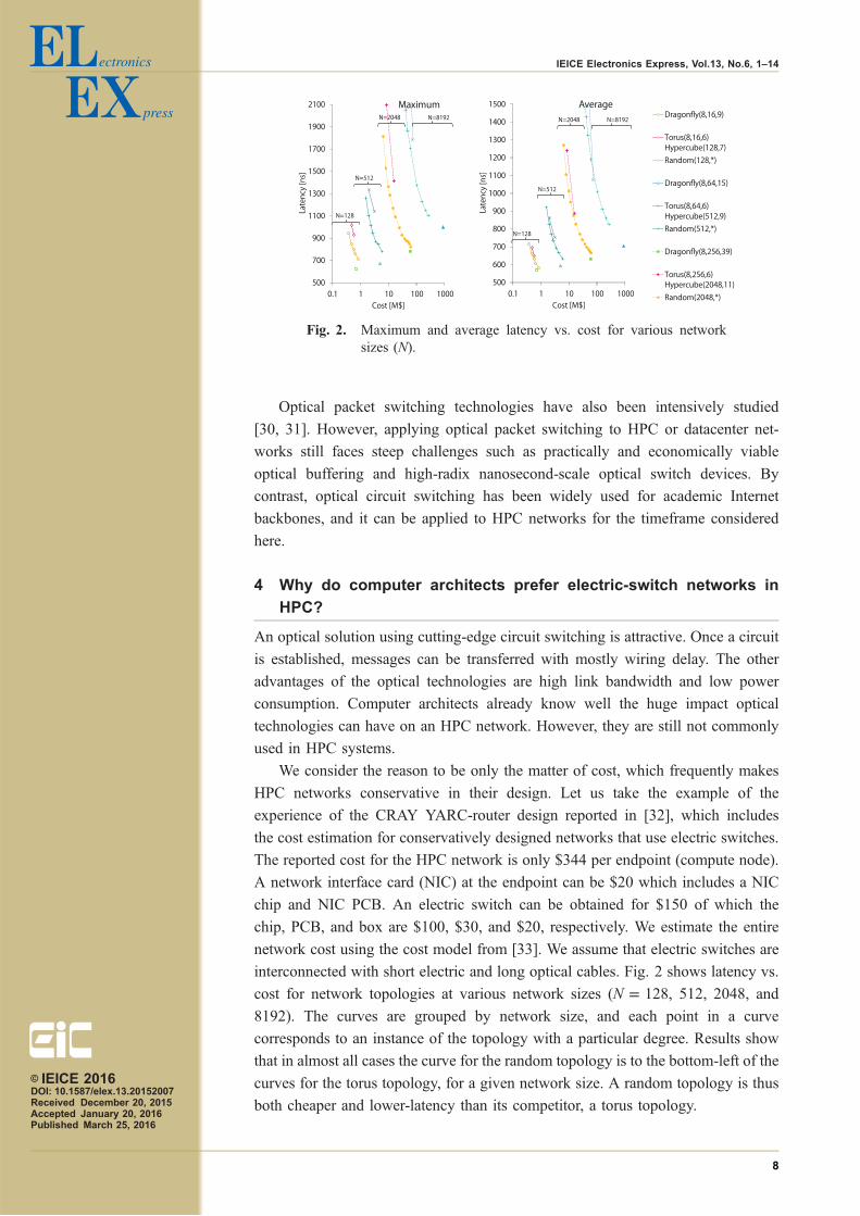
We consider the reason to be only the matter of cost, which frequently makes
HPC networks conservative in their design. Let us take the example of the
experience of the CRAY YARC-router design reported in [32], which includes
the cost estimation for conservatively designed networks that use electric switches.
The reported cost for the HPC network is only $344 per endpoint (compute node).
A network interface card (NIC) at the endpoint can be $20 which includes a NIC
chip and NIC PCB. An electric switch can be obtained for $150 of which the
chip, PCB, and box are $100, $30, and $20, respectively. We estimate the entire
network cost using the cost model from [33]. We assume that electric switches are
interconnected with short electric and long optical cables. Fig. 2 shows latency vs.
cost for network topologies at various network sizes (N ¼ 128, 512, 2048, and
8192). The curves are grouped by network size, and each point in a curve
corresponds to an instance of the topology with a particular degree. Results show
that in almost all cases the curve for the random topology is to the bottom-left of the
curves for the torus topology, for a given network size. A random topology is thus
both cheaper and lower-latency than its competitor, a torus topology.
Fig. 2. Maximum and average latency vs. cost for various networksizes (N).
© IEICE 2016DOI: 10.1587/elex.13.20152007Received December 20, 2015Accepted January 20, 2016Published March 25, 2016
8
IEICE Electronics Express, Vol.13, No.6, 1–14
Currently, advanced researches can provide a low hop-count topology and a
low-latency electric switch so that a 1 µs latency is achieved across the system. A
high link bandwidth can be obtained by active optical cables (AOCs), and electric
switch chips have had a 100-fold aggregate bandwidth improvement over 10 years
[34]. We consider that this conservative network architecture using electric switches
connected by AOCs will scale during the Moore’s law era. Feasible optical network
technologies should be more cost efficient than shown in Fig. 2 by the beginning of
the post-Moore era, though it might be difficult.
5 Challenge of optical HPC networks in postMoore era
Since Moore’s law will come to end by 2025–2030 due to physical constraints, the
aggregate bandwidth of the switch chip will be saturated. Instead of electric
switches, we will have to use optical switches, especially optical circuit switches,
in the post-Moore era. This will be a good opportunity to innovate the HPC
network architecture using optical technologies, assuming that optical technologies
continue to improve even in the post-Moore era. In this section we optimistically
illustrate our unique research vision for the post-Moore HPC networks using optical
network technologies. We introduce our three technology types that can work
together: wide-area optical technologies for low-latency and high-bandwidth com-
munications, WDM FSO for application optimization and cabling reduction, and
in-water HPC computers for ideal cooling.
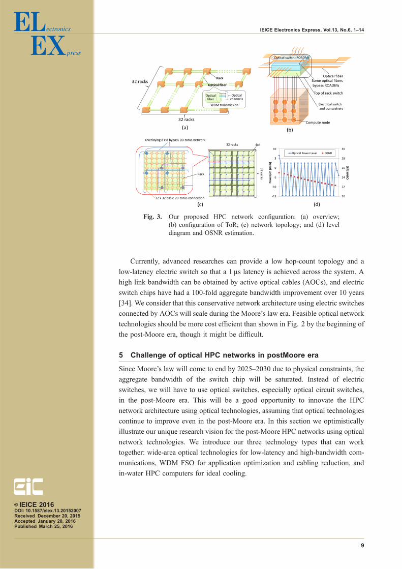
Fig. 3. Our proposed HPC network configuration: (a) overview;(b) configuration of ToR; (c) network topology; and (d) leveldiagram and OSNR estimation.
© IEICE 2016DOI: 10.1587/elex.13.20152007Received December 20, 2015Accepted January 20, 2016Published March 25, 2016
9
IEICE Electronics Express, Vol.13, No.6, 1–14

5.1 Using wide-area optical technologies on HPC networks
We consider and evaluate the scalability of an HPC network introducing a practical
reconfigurable optical add-drop multiplexer (ROADM) and WDM technologies
which are commonly used in wide-area broadband telecommunication networks.
Fig. 3 shows our proposed network configuration; WDM transmission is intro-
duced to inter-cabinet fiber connections (Fig. 3(a)); ROADMs are stored in ToRs
together with electric switches (Fig. 3(b)); and inter-cabinet network topology is
based on a 2D torus. Vital concerns for introducing optical switching technologies
such as ROADM into HPC interconnects are the limitation on the number of optical
switch ports and the optical signal degradation as a function of the number of
optical switches the optical signal transparently goes through. To resolve these
problems, we introduce bypass fiber connectivity, in which some fibers connecting
inter-cabinets bypass some intermediate ROADMs as shown in Fig. 3(c); the
bypass 2D torus networks overlay a basic 2D orus network connecting adjacent
cabinets. By introducing the overlaying bypass networks, the average number of
ROADMs the optical signals go through is reduced and higher-density connectivity
between the cabinets is enabled.
To estimate the practical scalability of the proposed architecture, we assume the
use of commercially available ROADM technologies, that is, the number of WSS
ports is assumed to 1 � 20 [35]. We assume that the total number of cabinets is
1,024 in an HPC system and they are allocated on a 32 � 32 2D array; 200 compute
nodes are accommodated in each cabinet; about two hundred-thousand compute
nodes are accommodated in total. With these assumption, setting the overlaying
2D torus networks as connecting every 4 ROADMs as shown in Fig. 3(c) and the
add/drop ratio at each node as 25%, the required scale ROADM can be configured
with 1 � 20WSSs. In this network topology, the maximum number of ROADMs an
optical signal goes through in the shortest path is less than 16. Fig. 3(d) shows the
designed level diagram and estimated optical signal to noise ratio (OSNR). After an
optical signal goes through 16 ROADMs, OSNR remains sufficiently large.
We estimate the throughput of each ToR as followings. We assume that each
compute node has 8 IOs; one of them is connected with ToR and the others are used
for intra-cabinet connections; line rate of each IO is 40Gbps. The optical signal
spacing of WDM transmission is assumed as 100GHz, which is wide enough to
avoid the optical filter narrowing effect, and accordingly the number of optical
signals accommodated by one fiber is 40 using C-band. The capacity of ROADMs
connecting cabinets is 25.6 Tbps (40 wavelengths � 16 degrees � 40Gbps). The
add/drop capacity in each ROADM is 6.4 Tbps (40 wavelengths � 4 fibers �40Gbps); the total capacity of the compute node IO which is connected with
ToR is 8 Tbps (40Gbps � 200 nodes); so that the oversubscription of 1.25 is
imposed on each cabinet. We can easily reduce the oversubscription by using the
WSSs with larger port counts which will soon become commercially available
(namely, before the post-Moore era).
© IEICE 2016DOI: 10.1587/elex.13.20152007Received December 20, 2015Accepted January 20, 2016Published March 25, 2016
10
IEICE Electronics Express, Vol.13, No.6, 1–14
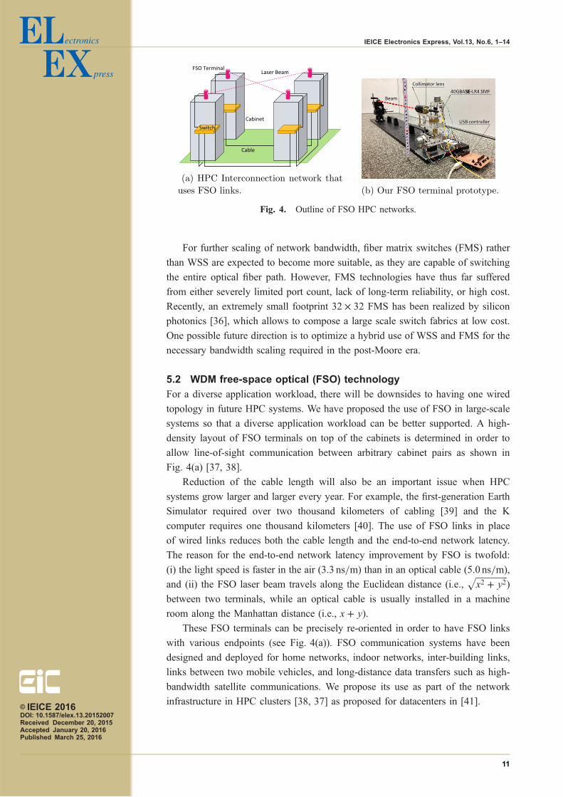
For further scaling of network bandwidth, fiber matrix switches (FMS) rather
than WSS are expected to become more suitable, as they are capable of switching
the entire optical fiber path. However, FMS technologies have thus far suffered
from either severely limited port count, lack of long-term reliability, or high cost.
Recently, an extremely small footprint 32 � 32 FMS has been realized by silicon
photonics [36], which allows to compose a large scale switch fabrics at low cost.
One possible future direction is to optimize a hybrid use of WSS and FMS for the
necessary bandwidth scaling required in the post-Moore era.
5.2 WDM free-space optical (FSO) technology
For a diverse application workload, there will be downsides to having one wired
topology in future HPC systems. We have proposed the use of FSO in large-scale
systems so that a diverse application workload can be better supported. A high-
density layout of FSO terminals on top of the cabinets is determined in order to
allow line-of-sight communication between arbitrary cabinet pairs as shown in
Fig. 4(a) [37, 38].
Reduction of the cable length will also be an important issue when HPC
systems grow larger and larger every year. For example, the first-generation Earth
Simulator required over two thousand kilometers of cabling [39] and the K
computer requires one thousand kilometers [40]. The use of FSO links in place
of wired links reduces both the cable length and the end-to-end network latency.
The reason for the end-to-end network latency improvement by FSO is twofold:
(i) the light speed is faster in the air (3.3 ns/m) than in an optical cable (5.0 ns/m),
and (ii) the FSO laser beam travels along the Euclidean distance (i.e.,ffiffiffiffiffiffiffiffiffiffiffiffiffiffiffix2 þ y2
p)
between two terminals, while an optical cable is usually installed in a machine
room along the Manhattan distance (i.e., x þ y).
These FSO terminals can be precisely re-oriented in order to have FSO links
with various endpoints (see Fig. 4(a)). FSO communication systems have been
designed and deployed for home networks, indoor networks, inter-building links,
links between two mobile vehicles, and long-distance data transfers such as high-
bandwidth satellite communications. We propose its use as part of the network
infrastructure in HPC clusters [38, 37] as proposed for datacenters in [41].
Fig. 4. Outline of FSO HPC networks.
© IEICE 2016DOI: 10.1587/elex.13.20152007Received December 20, 2015Accepted January 20, 2016Published March 25, 2016
11
IEICE Electronics Express, Vol.13, No.6, 1–14

Our prototype is shown in Fig. 4(b). Built with off-the-shelf motors and gears,
it is 360-degree steerable within 0.003-degree error, which translates into 1.6-mm
of positioning error at a distance of 30m, which is well within the 6-mm tolerance
of an FSO link [41]. Its footprint is 50mm across. Its height can be lowered. This
design thus greatly loosens the constraints in [41] regarding the number of possible
pairs of communicating FSO terminals. We have validated that our prototype
achieves error-free data transfers. Using iperf we also have measured an over
38Gbps bandwidth for 40GBASE-LR4 with jumbo frames using TCP streams.
Another work reported that the 100Gbps Ethernet signal transmission is demon-
strated with no particular degradation for 30-m indoor FSO link that uses 10-
channel DWDM technology [42]. We expect that the WDM FSO will be able to
work on any type of optical network.
5.3 Thin in-water optical cables for in-water HPC systems
The heat dissipation problem becomes critical for HPC systems, and is strongly
linked to their power consumption. Recently, fluid-submerged HPC systems using
mineral oil or Fluorinert have been developed for efficient cooling. However, the
cost to maintain the special cooling liquid can be high.
We consider that ultimate cooling of HPC systems can be achieved by the use
of natural water. What if an HPC system works in natural water, e.g., in a river or
in the ocean? Then heat would directly dissipate into the water and a power usage
effectiveness (PUE) of 1.00 would be easily achieved. To this end, we are
developing some waterproofing technologies that allows heat dissipation while
protecting the electric circuit from water (We have successfully demonstrated the
in-water computer and its operation for multiple days using the set-up shown in
Fig. 5). An interesting challenge for optical technologies with regard to in-water
computers is to make in-water optical cables thin for a high density layout of
compute nodes in an in-water HPC system.
Fig. 5. Our in-water computer prototype.
© IEICE 2016DOI: 10.1587/elex.13.20152007Received December 20, 2015Accepted January 20, 2016Published March 25, 2016
12
IEICE Electronics Express, Vol.13, No.6, 1–14
6 Conclusions
Current HPC systems conservatively use a packet network using low-latency
electric switches. We considered that this network architecture will have to be
abandoned by the beginning of the post-Moore era. In the post-Moore era, optical
technologies will be reborn in HPCs. We introduced our unique post-Moore vision
using wide-area optical technologies (for low-latency and high-bandwidth commu-
nications), WDM FSO (for application optimization and cabling reduction) and in-
water HPC computers (for ideal cooling).
Acknowledgments
This work is partially supported by SCOPE, JST CREST, Kakenhi # 25280018 and
the European Commission under the 7th Framework Programs through the Euro-
server (FP7-ICT-610456).
Michihiro Koibuchireceived the BE, ME, and PhD degrees from Keio University, Yokohama, Japan,in 2000, 2002 and 2003, respectively. Currently, he is an associate professor inthe Information Systems Architecture Research Division, National Institute ofInformatics and the Graduate University of Advanced Studies, Tokyo, Japan.His research interests include the area of high-performance computing andinterconnection networks. He is a member of the IEEE and a senior member ofIEICE and IPSJ.
Ikki Fujiwarareceived the BE and ME degrees from Tokyo Institute of Technology, Tokyo,Japan, in 2002 and 2004, respectively, and received the PhD degree from theGraduate University for Advanced Studies (SOKENDAI), Tokyo, Japan, in2012. He is currently a Project Assistant Professor in the Information SystemsArchitecture Research Division, National Institute of Informatics, Tokyo, Japan.His research interests include the areas of high-performance computing andoptimization. He is a member of the IPSJ, IEICE and IEEE.
Kiyo Ishiireceived the M.E. and D.E. degree in electrical and electronic engineering andcomputer science from Nagoya University, Nagoya, Japan, in 2008 and 2011,respectively. She is currently with the National Institute of Advanced IndustrialScience and Technology (AIST), Tsukuba, Japan. Her research interests includethe areas of photonic network system and optical node architecture. She is amember of IEICE and IEEE.
© IEICE 2016DOI: 10.1587/elex.13.20152007Received December 20, 2015Accepted January 20, 2016Published March 25, 2016
13
IEICE Electronics Express, Vol.13, No.6, 1–14

Shu Namikireceived MS, and Dr. Sci. in applied physics from Waseda University, Tokyo,Japan, in 1988 and 1998, respectively, and currently is Director of DataPhotonics Project Unit of the National Institute of Advanced Industrial Scienceand Technology (AIST), Tsukuba, Japan. He is also serving as Chair ofExecutive Committee of a national project called Vertically Integrated Center forTechnologies of Optical Routing toward Ideal Energy Savings (VICTORIES) incollaboration with ten telecom-related companies. His current research interestsinclude software defined dynamic optical path networking and their enablingdevices such as nonlinear fiber-optics and silicon photonics. Dr. Namiki is aFellow of OSA, and a member of IEICE, JSAP, and IEEE Photonics Society andCommunications Society.
Fabien Chaixreceived MS. and PhD. degrees from the Grenoble University, France,respectively in 2008 and 2013. He is currently a postdoctoral researcher in theCARV laboratory at FORTH-ICS, Heraklion, Greece. His research interestsinclude interconnect low-diameter topologies, resilience and simulation.
Hiroki Matsutanireceived the BA, ME, and PhD degrees from Keio University, Yokohama, Japan,in 2004, 2006, and 2008, respectively. He is currently an assistant professor inthe Department of Information and Computer Science, Keio University. Hisresearch interests include the areas of computer architecture and interconnectionnetworks. He is a member of the IPSJ, IEICE and IEEE.
Hideharu Amanoreceived the PhD degree from Keio University, Yokohama, Japan, in 1986. He iscurrently a professor in the Department of Information and Computer Science,Keio University. His research interests include the areas of parallel processingand reconfigurable systems. He is an IEEE member and an IEICE fellow.
Tomohiro Kudohreceived his BE, ME and Ph.D. degree from Keio University in Japan in 1986,1988 and 1992 respectively. He is currently a professor at the InformationTechnology Center, The University of Tokyo. Before joining the university in2015, he was at Tokyo University of Technology from 1991 to 1997, and theleader of Parallel and Distributed Architecture Tsukuba Laboratory of the RealWorld Computing Partnership from 1997 to 2002. Then he was at NationalInstitute of Advanced Industrial Science and Technology (AIST) from 2002 to2015, and served various positions at AIST including a director of InformationTechnology Research Institute.
© IEICE 2016DOI: 10.1587/elex.13.20152007Received December 20, 2015Accepted January 20, 2016Published March 25, 2016
14
IEICE Electronics Express, Vol.13, No.6, 1–14