Measurement setup for High Power Impulse Magnetron Sputtering

Appl. Phys. A 70, 457–459 (2000) / Digital Object Identifier (DOI) 10.1007/s003390000429 Applied Physics AMaterialsScience & Processing
Optical diffuse reflectance spectra ofGaSbnanocrystals embedded inSiO2 matrix by radio-frequency magnetron co-sputteringF.M. Liu, J.H. Jia, L.D. Zhang
Institute of Solid State Physics, Chinese Academy of Sciences, Hefei 230031, P.R. China(Fax: +86-551/559-1434, E-mail: [email protected])
Received: 28 July 1999/Accepted: 27 October 1999/Published online: 1 March 2000 – Springer-Verlag 2000
Abstract. NanocrystallineGaSbembedded inSiO2 films wasgrown by radio-frequency magnetron co-sputtering. X-raydiffraction pattern and transmission electron microscopy(TEM) confirm the existence ofGaSbnanocrystals in theSiO2 matrix. The average size ofGaSbnanoparticles is inthe range of 3 to11 nm. Diffuse reflectance spectra wereused to characterize the small change of the band gap of thesemiconductor. The diffuse reflectance spectra shows that theabsorption peaks have a large blueshift of about4.0 eV of theabsorption relative to that of bulkGaSb. It has been explainedby quantum confinement effects. Room temperature opticaltransmission spectra show that the absorption edge exhibitsa very large blueshift of about2.1 eV with respect to that ofbulk GaSbin agreement with quantum confinement.
PACS: 78.66.Fd; 78.20.Ci; 81.15.Cd
Photoreflectance (PR) measurements are of considerable in-terest since they are contactless, require no special mountingof the sample, and can be performed in a variety of trans-parent ambients [1, 2]. The PR spectra have already beenproven as a valuable characterization method in the case ofGaAs/GaAlAsheterojunction bipolar transistor (HBT) struc-tures [1–3] andInP/InGaAsHBT structures [4]. Reflectancedifference spectroscopy (RDS) was used to monitor crys-tal growth [5, 6]. However, little work on the applicationof diffuse reflectance spectra (DRS) to investigate semicon-ductor structures and semiconductor interfaces has been re-ported. In this paper we report a DRS study at room tem-perature ofGaSbnanocrystals embedded inSiO2 films byradio-frequency (RF) magnetron co-sputtering. The compos-ite films of GaSb-SiO2 were further characterized by X-raydiffraction (XRD) and by measuring transmission absorptionspectra.
1 Experimental procedure
A SiO2 glassy plate of60 mmin diameter containing severalchips of polycrystallineGaSbwas used as a target. The sub-
strates were ultrasonically washed successively in acetone,alcohol, and deionized water in order to obtain a clean surfacebefore being placed into a vacuum chamber. CleavedNaClsingle crystals were used for TEM observation. The cham-ber was evacuated to a final pressure of2.67×10−3 Pabeforethe high-purity (99.999%) argon gas was introduced. Dur-ing sputtering, the chamber pressure was maintained at1.5 Paand the argon gas flow was controlled by a gas valve. The out-put voltage of the RF sputter gun was1000 V. All runs startedwith presputtering of the target for10–15 min. A stainlesssteel strip was used as a substrate resistance heater, as well asa substrate holder. The substrate temperature was measuredby using a K-type Alumel–Chromel thermocouple mountedon the strip surface.
X-ray diffraction (XRD) profiles were collected at roomtemperature in the range of15–55◦C with D/max-rA diffrac-tometer, equipped with aCuKα anode at40 kV, 100 mA, andCPS 2000. The morphology and the average size of nanopar-ticles were investigated with an JEM-200CX transmissionelectron microscope (TEM). Room-temperature optical trans-mission spectra and diffuse reflectance spectra (DRS) wereperformed in a Cary 5E spectrophotometer in the range of 200to 2500 nm. The UV-VIS-NIR light was provided by xenonand tungsten lamps, selected by grating, spectral band width(SBW), and chopper. In our experiment, the SBW is set up0.01 to2.00 nm. A baseline is recorded with the polytetraflu-oroethylene (PTFE) reference disk covering the sample port.The sample is the mounted over the port and the reflectionoff the sample surface is collected by the110-mm integrat-ing sphere, the95-mm2 area lead sulfide (PbS) detector, andthe R928 photomultiplier tube (PMT) detector. The data ob-tained with the diffuse reflectance accessory (DRA) is relativeto the PTFE used to record the100% baseline. The DRSdata were obtained in full angle by a computer system, with900.00 nm/min scan rate and1-nmdata interval.
2 Results and discussions
Figure 1 gives X-ray diffraction patterns ofGaSb–SiO2 com-posite film, which was grown at400◦C for 3 h. The film
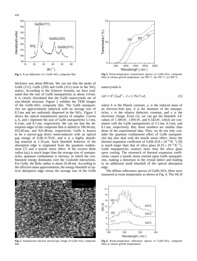
458
Fig. 1. X-ray diffraction of aGaSb–SiO2 composite film
thickness was about800 nm. We can see that the peaks ofGaSb(111), GaSb(220) andGaSb(311) exist in theSiO2matrix. According to the Scherrer formula, we have eval-uated that the size ofGaSbnanoparticles as about3.8 nm.It is clearly elucidated that theGaSb nanocrystals are ofzinc-blende structure. Figure 2 exhibits the TEM imagesof the GaSb–SiO2 composite film. TheGaSb nanoparti-cles are approximately spherical with an average size of8.3 nm and are uniformly dispersed in theSiO2. Figure 3shows the optical transmission spectra of samples. Curvesa, b, and c represent the size ofGaSbnanoparticles5.1 nm,6.3 nm, and 8.1 nm, respectively. We can see that the ab-sorption edges of the composite film is shifted to590.60 nm,655.83 nm, and 923.48 nm, respectively.GaSb is knownto be a narrow-gap direct semiconductor with an opticalgap energy of0.68–0.70 eV, and it is a highly absorb-ing material at1.35µm. Such blueshift behavior of theabsorption edge is originated from the quantum confine-ment [7] and a tensile stress effect. If the exciton Bohrradius (aB) is much larger than the average size of nanopar-ticles, quantum confinement is obvious, in which the con-finement energy dominates over the Coulomb interactions.For GaSb, the Bohr radius is about20.46 nm. According tothe effective-mass approximation, the energy blueshift of op-tical absorption edge versus the average size of theGaSb
Fig. 2. Transmission electron microscopic image ofGaSb–SiO2 compositefilm
Fig. 3. Room-temperature transmission spectra ofGaSb–SiO2 compositefilms at various growth temperature. (a)300◦C. (b) 350◦C. (c) 400◦C
nanocrystals is
∆E≈ h2/2µd2−2×1.76e2/εd , (1)
whereh is the Planck constant,µ is the reduced mass ofan electron–hole pair,d is the diameter of the nanopar-ticles, ε is the relative dielectric constant, ande is theelectronic charge. From (1), we can get the blueshift∆Evalues of1.300 eV, 1.091 eV, and0.543 eV, which are con-sistent with theGaSbnanoparticles of5.1 nm, 6.3 nm, and8.1 nm, respectively. But, these numbers are smaller thanthose of the experimental data. Thus, we do not only con-sider the quantum confinement effect ofGaSb nanoparti-cles but also deal with the tensile stress effect. Since thethermal expansion coefficient ofGaSb(6.8×10⁻⁶ K−1) [8]is much larger than that of silica glass (0.55×10⁻⁶ K−1),GaSb nanoparticles contract more than the silica glassupon cooling. The mismatch of thermal expansion coeffi-cients causes a tensile stress exerted uponGaSbnanoparti-cles, making a distortion in the crystal lattice and leadingto an additional small blueshift of the optical absorptionedge.
The diffuse reflectance spectra ofGaSb–SiO2 films weremeasured at room temperature as shown in Fig. 4. TheδR/R
Fig. 4. Room-temperature reflectance spectra ofGaSb–SiO2 compositefilms at various growth temperatures

459
can be defined as
δR/R= (Rs− R0)/R0 , (2)
where Rs is DRS of the sample with the composite filmsof GaSb–SiO2 upon the glass substrate, andR0 is the DRSof the glass substrate. It demonstrates the band gap varia-tion of composite films with the size ofGaSbnanoparticles.Figures 4a, 4b, and 4c correspond to growth temperature400◦C, 350◦C, and300◦C for 3 h, respectively. We can seethe small change of band gap of semiconductor with increas-ing the growth temperature. Figure 4 shows that there aremany reflectance peaks at294.0 nm, 304.5 nm, 313.0 nm, and321.7 nm, which depend on the size ofGaSbnanocrystals.The reflectance peaks are coincident with [9]. The blueshift ofthe reflectance peak is due to the quantum confinement effect.
Ideal diffuse reflection is defined by the condition that theangular distribution of the reflected radiation is independentof the angle of incidence [10]. For the simplest case of per-pendicular incidence, the diffuse reflectance can be definedas
R= [(n−1)2+n2κ2] / [(n+1)2+n2κ2] , (3)
wheren is the refractive index, andκ is the extinction coef-ficient related to the absorption coefficientα by α = 4πκ/λ(λ is incident light wavelength). The larger the absorption co-efficient, α, the larger becomesR. The regular part of thereflection at the Bouguer elementary mirrors must already, forperpendicular incidence on absorbing materials, be more no-ticeable than on nonabsorbent materials. At large angles ofincidence the influence ofα on Rmust greatly increase so thatR eventually approaches the limiting value of 1. The directenergy gaps can be extracted by [11]
αhν = A(hν− Eg)1/2 , (4)
where A is a constant andEg is energy gap of semicon-ductor. ForGaSbnanocrystals of3–10 nm, the confinementenergy dominates over the Coulomb interactions. From (2),(3), and (4), the reflectance peak blueshift can be explained.
So, it is convenient to evaluate the variation of energy gapof nanocrystal semiconductor by means of the diffuse re-flectance spectra.
3 Conclusions
We have successfully prepared the composite films ofGaSbnanocrystals embedded in aSiO2 matrix by radio-frequencymagnetron co-sputtering. We introduced DRS to character-ize the band gap of semiconductor. The diffuse reflectancespectra shows that the reflectance peak has a large blueshiftof about4.0 eV compared with that of bulkGaSb, which isexplained by quantum confinement effect. Room-temperatureoptical transmission shows that the absorption edge exhibitsa very large blueshift of about2.1 eV with respect to that ofbulk GaSbresulting in the quantum confinement effect.
Acknowledgements.This work was supported by the Climbing Program ofChina.
References
1. X. Yin, F.H. Pollak, L. Pawlowicz, T. O’Neill, M. Hafizi: Appl. Phys.Lett. 56, 1278 (1990)
2. N. Bottka, D.K. Gaskill, R.S. Sillmon, R. Henry, R. Glosser: J. Elec-tron. Mater.17, 161 (1988)
3. N. Bottka, D.K. Gaskill, P.D. Wright, R.W. Kaliski, D.A. Williams:J. Crystal Growth107, 893 (1991)
4. D. Yan, F.H. Pollak, V.T. Boccio, C.L. Lin, P.D. Kirchner, J.M. Woodall,R.C. Gee, P.M. Asbeck: Appl. Phys. Lett.61, 2066 (1992)
5. E. Colas, D.E. Aspnes, R. Bhat, A.A. Studna, J.P. Harbison, L.T. Flo-rez, M.A. Koza, V.G. Keramidas: J. Crystal Growth107, 47 (1991)
6. N. Kobayashi, T. Makimoto, Y. Yamauchi, Y. Horikoshi: J. CrystalGrowth 107, 62 (1991)
7. L.E. Brus: J. Phys. Chem.80, 4403 (1984)8. C. Raisin, A. Rocher, G. Landa, R. Carles, L. Lassabatere: Appl. Surf.
Sci. 50, 434 (1991)9. D.E. Aspnes, A.A. Studna: Phys. Rev. B27 985 (1983)
10. G. Kortum:Reflectance Spectroscopy: Principles, Methods, Applica-tions (Springer, New York 1969) p. 25
11. S.A. Abd El-Hady: Phys. Status Solidi A149, 601 (1995)