
OPTICAL AND INFRARED DETECTORS FOR...
32
OPTICAL AND INFRARED DETECTORS FOR ASTRONOMY Basic principles to state-of-the-art James W. Beletic Rockwell Scientific Company 5212 Verdugo Way Camarillo, Ca 93012 U.S.A. [email protected] Abstract Detectors play a key role in an astronomical observatory. In astronomy, the role of the telescope and instrument is to bring light to a focus - in effect, the telescope-instrument act as “spectacles”. The detectors, meanwhile, have the critical role of sensing the light - the detectors are the “eyes” of an observatory. The performance of an astronomical observatory is directly dependent upon the performance of its detector systems. In many ways, today’s optical and infrared detectors are nearly perfect, with high quantum efficiency, low readout noise, high dynamic range and large arrays of pixels. However, as good as the detectors are, there are limitations that must be understood and respected in order to produce the best astronomical instru- ments and thereby, the best science. This chapter explains how optical and infrared detectors work, from basic principles to the state-of-the-art. The role of optical and infrared detectors in an observatory is presented, and the state-of-the-art is related to an ideal detector. An overview of the detector physics is presented, showing that the detection of light is a 5 step process. Each step in this process is explained in detail in the sub- sequent sections. The chapter concludes with references for further information. Keywords: detectors, optical, infrared, quantum efficiency, noise 1. The role of detectors in astronomy Astronomy is a vibrant science, with significant new discoveries about the universe being made every year. Fueling these scientific breakthroughs are technological advances in many areas, from the new generation of 8-10 meter 123 R. Foy and F. C. Foy (eds.), Optics in Astrophysics, 123 © 2006 Springer. Printed in the Netherlands. –153.
Transcript of OPTICAL AND INFRARED DETECTORS FOR...
OPTICAL AND INFRARED DETECTORS FORASTRONOMYBasic principles to state-of-the-art
James W. BeleticRockwell Scientific Company5212 Verdugo WayCamarillo, Ca 93012 [email protected]
Abstract Detectors play a key role in an astronomical observatory. In astronomy, therole of the telescope and instrument is to bring light to a focus - in effect, thetelescope-instrument act as “spectacles”. The detectors, meanwhile, have thecritical role of sensing the light - the detectors are the “eyes” of an observatory.The performance of an astronomical observatory is directly dependent upon theperformance of its detector systems.In many ways, today’s optical and infrared detectors are nearly perfect, with
high quantum efficiency, low readout noise, high dynamic range and large arraysof pixels. However, as good as the detectors are, there are limitations that mustbe understood and respected in order to produce the best astronomical instru-ments and thereby, the best science.This chapter explains how optical and infrared detectors work, from basic
principles to the state-of-the-art. The role of optical and infrared detectors in anobservatory is presented, and the state-of-the-art is related to an ideal detector.An overview of the detector physics is presented, showing that the detection oflight is a 5 step process. Each step in this process is explained in detail in the sub-sequent sections. The chapter concludes with references for further information.
Keywords: detectors, optical, infrared, quantum efficiency, noise
1. The role of detectors in astronomyAstronomy is a vibrant science, with significant new discoveries about the
universe being made every year. Fueling these scientific breakthroughs aretechnological advances in many areas, from the new generation of 8-10 meter
123
R. Foy and F. C. Foy (eds.), Optics in Astrophysics, 123© 2006 Springer. Printed in the Netherlands.
–153.
124 OPTICS IN ASTROPHYSICS
Figure 1. A ground-based astronomical observatory can be depicted as having four major part:telescope, adaptive optics (optional), instrument optics, and the detector.
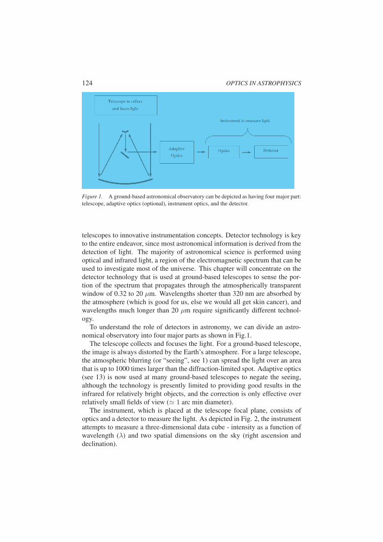
telescopes to innovative instrumentation concepts. Detector technology is keyto the entire endeavor, since most astronomical information is derived from thedetection of light. The majority of astronomical science is performed usingoptical and infrared light, a region of the electromagnetic spectrum that can beused to investigate most of the universe. This chapter will concentrate on thedetector technology that is used at ground-based telescopes to sense the por-tion of the spectrum that propagates through the atmospherically transparentwindow of 0.32 to 20 µm. Wavelengths shorter than 320 nm are absorbed bythe atmosphere (which is good for us, else we would all get skin cancer), andwavelengths much longer than 20 µm require significantly different technol-ogy.To understand the role of detectors in astronomy, we can divide an astro-
nomical observatory into four major parts as shown in Fig.1.The telescope collects and focuses the light. For a ground-based telescope,
the image is always distorted by the Earth’s atmosphere. For a large telescope,the atmospheric blurring (or “seeing”, see 1) can spread the light over an areathat is up to 1000 times larger than the diffraction-limited spot. Adaptive optics(see 13) is now used at many ground-based telescopes to negate the seeing,although the technology is presently limited to providing good results in theinfrared for relatively bright objects, and the correction is only effective overrelatively small fields of view ( 1 arc min diameter).The instrument, which is placed at the telescope focal plane, consists of
optics and a detector to measure the light. As depicted in Fig. 2, the instrumentattempts to measure a three-dimensional data cube - intensity as a function ofwavelength (λ) and two spatial dimensions on the sky (right ascension anddeclination).

125
Figure 2. Three-dimensional data cube that is probed by an astronomical instrument: the in-tensity is a function of two spatial directions on the sky (right ascension and declination - anal-ogous to longitude and latitude) and the wavelength dimension.
A major challenge for instrumentation comes from detectors being “col-orblind”. All optical and infrared detector arrays, from the human eye andphotographic film to the state-of-the-art used on astronomical telescopes, canonly measure intensity and not wavelength. Every photon detected by an opti-cal or infrared detector produces an electron, and all electrons look the same,whether produced by a short or long wavelength photon. In a similar way,the rods and cones in the human eye only sense intensity. Color perception isdue to subsets of rods and cones having sensitivity to specific colors. Thus,a focal plane array can not simultaneously measure the full three-dimensionaldata cube shown in Fig. 2. A significant challenge for an instrument builderis designing optics that efficiently sample a 2-D portion of the 3-D data cube.There are several ways to select a 2-D portion of the data cube:
Imaging: uses a filter to take an image in a limited wavelength band.
Spectroscopy: 3 types are used in astronomy:
a slit spectrograph which places a slit (e.g., 1 arc sec wide by 30arc sec long) at the focal plane to filter out a 1-D slice of the skyand disperses the spectrum in the orthogonal direction,a multi-object spectrograph that spatially filters the image with sev-eral small slits in the image plane and disperses the spectra in theorthogonal direction (in many cases, none of the slits can overlapin the spatial direction),an integral field spectrograph samples a contiguous 2-D array ofspatial pixels and uses lenses, fibers or mirrors to align the light so
Optical and Infrared Detectors for Astronomy

126 OPTICS IN ASTROPHYSICS
that when it is dispersed spectrally, the individual pixel spectra donot overlap.
The promise of 3-D detectors: The ideal detector would be able to measure the wavelengthdimension of each photon in addition to the two spatial dimensions - a “3-D detector”. Thereis progress being made on 3-D detectors - for example, the superconducting tunneling junction(STJ). However, at present, 3-D detectors are experimental and have only achieved limitedwavelength resolution (λ/δλ ≤ 25) with relatively slow count rates (few kHz per pixel) on asmall number of pixels ( 100). Since these devices are experimental and are not being usedin a facility instrument at any telescope, we do not discuss them further in this chapter.
This chapter will concentrate on the very high quality detectors that areneeded in scientific imagers and spectrographs, and other applications thatrequire high sensitivity, such as acquisition and guiding, adaptive optics andinterferometry. We limit our discussion to focal plane arrays – large two-dimensional arrays of pixels – as opposed to single pixel detectors (e.g., aval-anche photodiodes).Note that there are many other applications of detectors in an astronomical
observatory, including detectors that are used for active optics, site monitoring(seeing, cloud cover), surveillance and safety monitoring.It is easy to conclude that detectors are one of the most critical technologies
in astronomy. Thus, for an observatory to take a leading role in astronomicalresearch, it must ensure that it has expertise and adequate resources allocatedto this area.
2. The ideal detector and the state-of-the-artIdeally, an observatory would install perfect detectors in the focal plane of
its instruments. What makes a perfect detector? The attributes of an ideal de-tector and the performance achieved by today’s technology are given in Table1. Optical and infrared detectors are nearly ideal in several ways:
Quantum efficiency (QE) - The sensitivity of a detector can be nearlyperfect, with up to 99% of the photons detected at the wavelength forwhich the detector is optimized.Delta function response - Over most of the wavelengths of interest, opti-cal and infrared detectors produce one photoelectron for every detectedphoton, which provides a one-to-one correspondence between detectedphotons and photoelectrons. This means that the detector response isexactly linear to the intensity incident on the detector – an attribute thatallows astronomers to precisely remove sky background and electronicbias to accurately measure the intensity of the astronomical object.Large number of pixels - A very large number of pixels can now be inte-grated on a single focal plane. The largest array presently in operation in
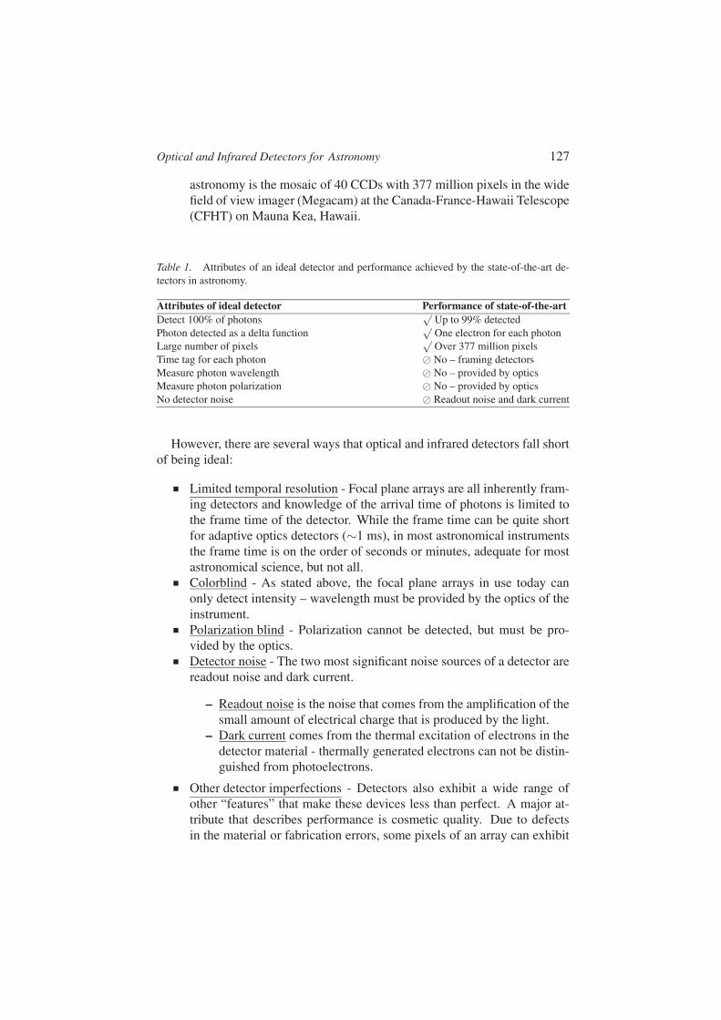
Optical and Infrared Detectors for Astronomy 127
astronomy is the mosaic of 40 CCDs with 377 million pixels in the widefield of view imager (Megacam) at the Canada-France-Hawaii Telescope(CFHT) on Mauna Kea, Hawaii.
Table 1. Attributes of an ideal detector and performance achieved by the state-of-the-art de-tectors in astronomy.
Attributes of ideal detector Performance of state-of-the-artDetect 100% of photons
√Up to 99% detected
Photon detected as a delta function√One electron for each photon
Large number of pixels√Over 377 million pixels
Time tag for each photon No – framing detectorsMeasure photon wavelength No – provided by opticsMeasure photon polarization No – provided by opticsNo detector noise Readout noise and dark current
However, there are several ways that optical and infrared detectors fall shortof being ideal:
Limited temporal resolution - Focal plane arrays are all inherently fram-ing detectors and knowledge of the arrival time of photons is limited tothe frame time of the detector. While the frame time can be quite shortfor adaptive optics detectors (∼1 ms), in most astronomical instrumentsthe frame time is on the order of seconds or minutes, adequate for mostastronomical science, but not all.Colorblind - As stated above, the focal plane arrays in use today canonly detect intensity – wavelength must be provided by the optics of theinstrument.Polarization blind - Polarization cannot be detected, but must be pro-vided by the optics.Detector noise - The two most significant noise sources of a detector arereadout noise and dark current.
– Readout noise is the noise that comes from the amplification of thesmall amount of electrical charge that is produced by the light.– Dark current comes from the thermal excitation of electrons in thedetector material - thermally generated electrons can not be distin-guished from photoelectrons.
Other detector imperfections - Detectors also exhibit a wide range ofother “features” that make these devices less than perfect. A major at-tribute that describes performance is cosmetic quality. Due to defectsin the material or fabrication errors, some pixels of an array can exhibit

128 OPTICS IN ASTROPHYSICS
Figure 3. Optical and infrared detector “zoology”. The wavelength region is stated on the firstrow, with corresponding wavelength (in µm) shown on the second row. The type of detectormaterial and associated manufacturers are shown in the boxes below, which also depict thewavelength coverage possible with each kind of detector material.
lower QE, and in the worst case, be completely dead. Also, some pixelswill exhibit excessively high dark current. In a CCD, an extremely badpixel can make an entire column useless, and thus, the primary measureof cosmetic quality for a CCD is the number of bad columns.
3. Detector zoologyOptical and infrared detectors can be organized into the “zoology” presented
in Fig. 3. The wavelength regions included in the graph are x-ray, optical (0.3- 1.1 µm), near infrared (NIR, 1-5 µm) and mid-infrared (MIR, 5-20 µm).For detection of optical light, silicon (Si) is the best material, and there areseveral designers and manufacturers of silicon-based detectors. In the nearinfrared, two materials are used for focal plane arrays: Mercury-Cadmium-Telluride (HgCdTe), also known as “Mer-Cad-Tel”, and Indium-Antimonide(InSb). In the mid-infrared, arsenic doped silicone is used. In the infrared,there is limited choice of manufacturer; only Raytheon Vision Systems andRockwell Scientific have a significant presence.
4. Detector architecture and operation: 5 steps of lightdetection
In this section, an overview of detector architecture and operation is given.Although optical and infrared detectors are often thought of as very differentbeasts, in practice they are more alike than different. Thus, optical and infrared
Optical and Infrared Detectors for Astronomy 129
Figure 4. Simplified schematic of an optical/infrared focal plane array. The detector is a thinwafer of light sensitive material that is connected to a thin layer of solid state electronics - theconnection is made either by direct deposition (CCD) or bump bonding (IR detector). The solidstate electronics amplify and read out the charge produced by the incident light.
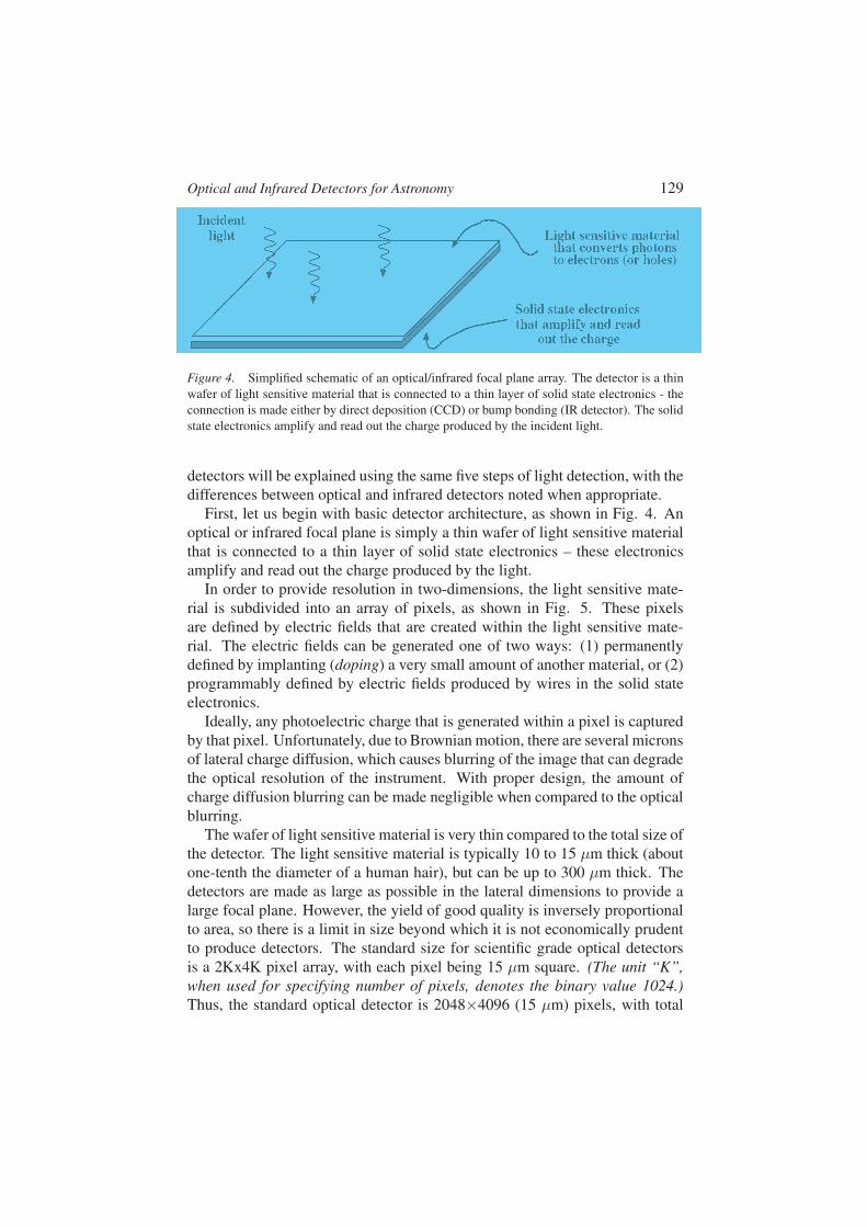
detectors will be explained using the same five steps of light detection, with thedifferences between optical and infrared detectors noted when appropriate.First, let us begin with basic detector architecture, as shown in Fig. 4. An
optical or infrared focal plane is simply a thin wafer of light sensitive materialthat is connected to a thin layer of solid state electronics – these electronicsamplify and read out the charge produced by the light.In order to provide resolution in two-dimensions, the light sensitive mate-
rial is subdivided into an array of pixels, as shown in Fig. 5. These pixelsare defined by electric fields that are created within the light sensitive mate-rial. The electric fields can be generated one of two ways: (1) permanentlydefined by implanting (doping) a very small amount of another material, or (2)programmably defined by electric fields produced by wires in the solid stateelectronics.Ideally, any photoelectric charge that is generated within a pixel is captured
by that pixel. Unfortunately, due to Brownian motion, there are several micronsof lateral charge diffusion, which causes blurring of the image that can degradethe optical resolution of the instrument. With proper design, the amount ofcharge diffusion blurring can be made negligible when compared to the opticalblurring.The wafer of light sensitive material is very thin compared to the total size of
the detector. The light sensitive material is typically 10 to 15 µm thick (aboutone-tenth the diameter of a human hair), but can be up to 300 µm thick. Thedetectors are made as large as possible in the lateral dimensions to provide alarge focal plane. However, the yield of good quality is inversely proportionalto area, so there is a limit in size beyond which it is not economically prudentto produce detectors. The standard size for scientific grade optical detectorsis a 2Kx4K pixel array, with each pixel being 15 µm square. (The unit “K”,when used for specifying number of pixels, denotes the binary value 1024.)Thus, the standard optical detector is 2048×4096 (15 µm) pixels, with total

130 OPTICS IN ASTROPHYSICS
Light sensitive materialis electrically partitionedinto a 2-D array of pixels
(each pixel is a 3-D volume)
Solid state electronicsthat amplify and read
out the chargex
y
z
Light sensitive materialis electrically partitionedinto a 2-D array of pixels
(each pixel is a 3-D volume)
Solid state electronicsthat amplify and read
out the charge
Solid state electronicsthat amplify and read
out the chargex
y
z
Figure 5. Simplified schematic of the 2-D array of pixels in a focal plane array. The thin waferof light sensitive material is partitioned into a two-dimensional array of pixels that collect theelectric charge produced by the light. Each pixel is a three-dimensional volume that is definedby electric fields within the light sensitive material.
dimension of 3.1×6.1 cm2, and a thickness of 15 µm. The largest infrareddetectors manufactured today are 2K×2K, 18 µm pixels (3.7×3.7 cm2) and 10to 15 µm thick.Since the photosensitive material and the electronics layer are very thin,
the detector is mounted on a mechanical package for structural integrity. Thispackage is thermally matched to the detector so that the detector will not bestretched or compressed during the large transition from room temperature tooperating temperature.With this basic understanding of the geometry of a detector, we can present
the five basic steps in optical/IR photon detection. The steps listed belowfollow the framework taught by James Janesick (2001) in his classic “CCDcourse”.
1 Get the light into the detector. This may sound trivial, but unless a goodanti-reflection coating is used, a significant fraction of the light will bereflected at the surface of the photosensitive material.2 Charge generation. Once the light is within the volume of the photosen-sitive material, the photon energy must be absorbed and converted tocharge. The photon energy creates electron-hole pairs.3 Charge collection. Electric fields within the photosensitive material col-lect charge into pixels. The detector can be designed to collect eitherelectrons or holes.4 Charge transfer. In the infrared, no charge transfer is required. For anoptical CCD, the charge is moved to the edge of the detector where theamplifiers are located.5 Charge amplification. Very small amounts of charge must be amplifiedbefore it can be digitized and transfered to a computer. Amplificationis a noisy process. At present, CCD amplifiers exhibit lower noise thaninfrared amplifiers.
Optical and Infrared Detectors for Astronomy 131
The first two steps, getting light into the detector and charge generation,affect quantum efficiency. The point spread function (PSF) of a detector is af-fected by the 3rd and 4th steps (charge collection and charge transfer). Unlessproper attention is paid to the PSF of a detector, poor PSF can negate the heroicefforts of optical designers who strive to maintain a tight PSF through the in-strument optics. All five steps affect the sensitivity of a detector, with differentsteps dominating the sensitivity at different light levels. At high light level, thesensitivity is primarily a function of quantum efficiency and PSF. At low lightlevel, the noise due to amplification dominates the sensitivity of a detector.The next sections will expand on the physics of the five steps listed above.
As much as possible, the explanation of optical and infrared detectors will becombined.
5. Getting light into the detector: anti-reflection coatingsThe velocity of light is a function of the material through which it travels.
The speed of light in a vacuum, denoted by c, is 2.998·108 m·s−1. The velocityof light v in a medium other than vacuum is given by,
v = c/n (1)
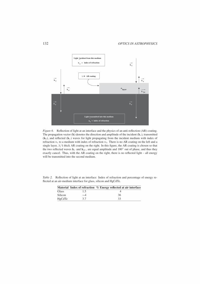
where n is the index of refraction for the medium (n = 1 for a vacuum).When light encounters a change in the index of refraction, some of the lightis transmitted and some is reflected, as shown in Fig.6 (left). For propagationperpendicular to the interface, the fraction of incident energy that is reflectedis given by,
Reflected energy = ((nt − ni) / (nt + ni))2 (2)
The index of refraction and amount of light reflected at an interface with air(nair ∼ 1.00) is given in Table 2. Note that the index of refraction of siliconvaries significantly over the 0.32-1.1 µm range, as shown in Fig.10; nSi ∼ 4applies for 0.5-0.9 µm.As shown in Table 2 and Eq. 2, a significant amount of light is lost due
to reflection at an interface when there is a large change in the index of re-fraction. Whenever light undergoes a sudden change in velocity, energy is
132 OPTICS IN ASTROPHYSICS
Figure 6. Reflection of light at an interface and the physics of an anti-reflection (AR) coating.The propagation vector (k) denotes the direction and amplitude of the incident (ki), transmitted(kt), and reflected (kr) waves for light propagating from the incident medium with index ofrefraction ni to a medium with index of refraction nt. There is no AR coating on the left and asingle layer, λ/4 thick AR coating on the right. In this figure, the AR coating is chosen so thatthe two reflected waves kr and k2r , are equal amplitude and 180 out of phase, and thus theyexactly cancel. Thus, with the AR coating on the right, there is no reflected light – all energywill be transmitted into the second medium.
Table 2. Reflection of light at an interface: Index of refraction and percentage of energy re-flected at an air-medium interface for glass, silicon and HgCdTe.
Material Index of refraction % Energy reflected at air interfaceGlass 1.5 4Silicon ∼4 36HgCdTe 3.7 33
nlayerk r
k i
n = index of refractioni
Light incident from this medium
k r k r
k i
k r
k r2
λ /4 AR coating
Light transmitted into this medium
n = index of refractiont

Optical and Infrared Detectors forAstronomy 133
reflected. The amount of energy that is reflected increases as the change invelocity increases. The amount of light that is transmitted and reflected isrigorously computed using the laws of electromagnetic propagation and conti-nuity of fields – on a more intuitive level, the amount of energy reflected at aninterface can be understood by analogy. Nearly all physical systems, as well ashuman interactions, do not adapt well to a sudden change in conditions – thegreater the change in direction or speed, the greater the amount of energy thatis “reflected”.The amount of energy that is reflected can be significantly reduced by use of
an anti-reflection coating (AR coating). An AR coating provides a smoothertransition from one medium to another, and can be used to provide zero reflec-tion at a selected wavelength (see 19). The simplest example of an AR coatingis the single layer coating shown on the right side of Fig. 6. If the AR coatingis λ/4 thick, then the amount of energy reflected is given by,
Reflected energy =
(nint − n2
layer
nint + n2layer
)2
(3)
where nlayer is the index of refraction of the AR coating. For an AR coatingwhere n2
layer = nint, there is no energy reflected - all of the light is transmittedinto the medium! An intuitive way to understand the physics is as follows.Light is indeed reflected at both interfaces, but the amount of energy reflected isthe same at each interface. Since the AR coating is λ/4 thick, the two reflectedwaves are 180 out of phase and they exactly cancel each other, resulting inzero energy being reflected back into the incident medium.Unfortunately, 100% transmission only occurs at a single wavelength, since
the AR coating can only be λ/4 thick for a single wavelength. Some manufac-turers use multi-layer coatings to obtain better results over a broader bandpassbut, for CCDs, the maximum is typically a two-layer AR coating. When select-ing an AR coating material, the optical designer tries to achieve the followinggoals: the coating is 100% transmissive for the wavelengths of interest, theindex of refraction of the coating is intermediate between air and the detectormaterial, and the AR coating can be applied with the coating technology avail-able. The most popular AR coating for silicon (nSi ∼ 4) is hafnium oxide(HfO2, nHfO2 ∼ 1.9). Figure 13 presents the results of detailed modelingof the effect of HfO2 coating thickness on QE. For IR detectors, Zinc sulfide(SZn) can be used as an AR coating (nSZn ∼ 2.27, nHgCdTe ∼ 3.7).A purchaser of scientific grade detectors needs to give careful attention to
the selection and tuning of AR coatings. The AR coating is one of the mostimportant specifications in a detector procurement.
134 OPTICS IN ASTROPHYSICS
Table 3. Energy (in eV) of optical and IR photons
Wavelength (µm) Energy (eV)0.3 4.130.5 2.480.7 1.771.0 1.242.5 0.505.0 0.2510.0 0.1220.0 0.06
6. Charge generationAfter the light has entered the material, it can be “detected”. The energy
of the electromagnetic field is extracted in quanta called photons with energygiven by Photon energy = hν, where h is the Planck constant (6.626 · 10−34
Js) and the frequency ν of light is related to the wavelength by ν = c/λ.Since a Joule (J) is a relatively large unit of energy, the electron-volt (1 eV =1.602 · 10−19 J) is typically used to express the energy of optical and infraredphotons, as shown in Table 3.
6.1 The photovoltaic effectThe detector materials discussed in this chapter are crystalline structures.
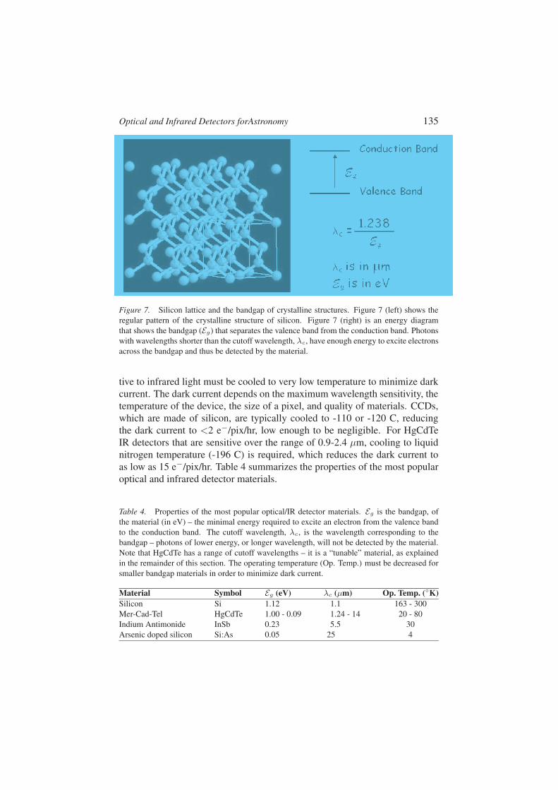
A crystal lattice is a regular, repetitive, three-dimensional pattern of the con-stituent atoms, as shown in Fig. 7 (left) for silicon. A crystal structure is tightlybound together by covalent bonds, which is the sharing of the outer electronsof adjacent atoms. These valence band electrons can be excited so that theyescape from the hold of the crystal lattice and are free to move through thematerial in the conduction band. When a “free electron” is created, a corre-sponding hole (vacancy of electron, or positive charge site) is also created. Anelectron-hole pair can be created from the absorption of the energy of a photonor from thermal energy. When the electron-hole pair is created by light, theprocess is called the photovoltaic effect. When the electron-hole pair is createdby thermal energy, the resulting flow of charge is called dark current.The amount of energy that is required to excite an electron from the valence
band to the conduction band is the bandgap (Eg) of the material; see Fig. 7(right). The wavelength (in microns) of the lowest energy photon that can bedetected by a material is given by the energy of a 1 µm photon divided by thebandgap of the material (in Eg) – this is called the cutoff wavelength, λc. To de-tect longer wavelength light, the bandgap must be smaller. A smaller bandgapalso makes it easier for thermal energy to excite electrons, so materials sensi-
Optical and Infrared Detectors forAstronomy 135
Figure 7. Silicon lattice and the bandgap of crystalline structures. Figure 7 (left) shows theregular pattern of the crystalline structure of silicon. Figure 7 (right) is an energy diagramthat shows the bandgap (Eg) that separates the valence band from the conduction band. Photonswith wavelengths shorter than the cutoff wavelength, λc, have enough energy to excite electronsacross the bandgap and thus be detected by the material.
tive to infrared light must be cooled to very low temperature to minimize darkcurrent. The dark current depends on the maximum wavelength sensitivity, thetemperature of the device, the size of a pixel, and quality of materials. CCDs,which are made of silicon, are typically cooled to -110 or -120 C, reducingthe dark current to <2 e−/pix/hr, low enough to be negligible. For HgCdTeIR detectors that are sensitive over the range of 0.9-2.4 µm, cooling to liquidnitrogen temperature (-196 C) is required, which reduces the dark current toas low as 15 e−/pix/hr. Table 4 summarizes the properties of the most popularoptical and infrared detector materials.
Table 4. Properties of the most popular optical/IR detector materials. Eg is the bandgap, ofthe material (in eV) – the minimal energy required to excite an electron from the valence bandto the conduction band. The cutoff wavelength, λc, is the wavelength corresponding to thebandgap – photons of lower energy, or longer wavelength, will not be detected by the material.Note that HgCdTe has a range of cutoff wavelengths – it is a “tunable” material, as explainedin the remainder of this section. The operating temperature (Op. Temp.) must be decreased forsmaller bandgap materials in order to minimize dark current.
Material Symbol Eg (eV) λc (µm) Op. Temp. (K)Silicon Si 1.12 1.1 163 - 300Mer-Cad-Tel HgCdTe 1.00 - 0.09 1.24 - 14 20 - 80Indium Antimonide InSb 0.23 5.5 30Arsenic doped silicon Si:As 0.05 25 4
136 OPTICS IN ASTROPHYSICS
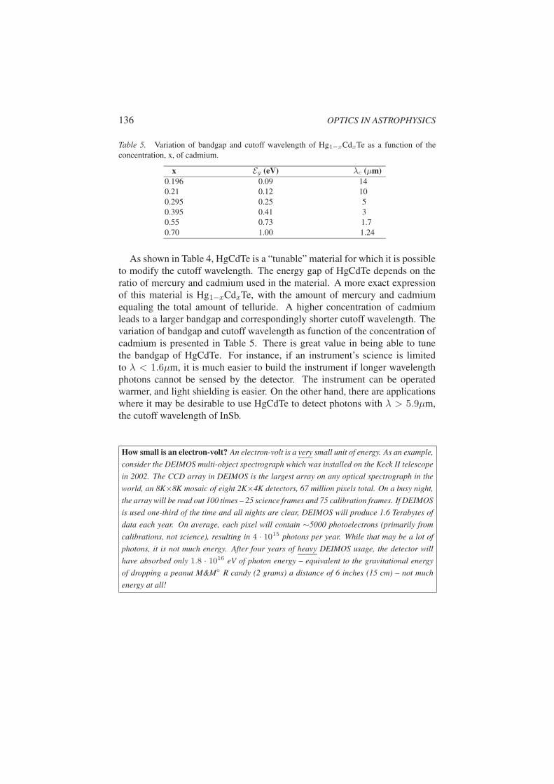
Table 5. Variation of bandgap and cutoff wavelength of Hg1−xCdxTe as a function of theconcentration, x, of cadmium.
x Eg (eV) λc (µm)0.196 0.09 140.21 0.12 100.295 0.25 50.395 0.41 30.55 0.73 1.70.70 1.00 1.24
As shown in Table 4, HgCdTe is a “tunable” material for which it is possibleto modify the cutoff wavelength. The energy gap of HgCdTe depends on theratio of mercury and cadmium used in the material. A more exact expressionof this material is Hg1−xCdxTe, with the amount of mercury and cadmiumequaling the total amount of telluride. A higher concentration of cadmiumleads to a larger bandgap and correspondingly shorter cutoff wavelength. Thevariation of bandgap and cutoff wavelength as function of the concentration ofcadmium is presented in Table 5. There is great value in being able to tunethe bandgap of HgCdTe. For instance, if an instrument’s science is limitedto λ < 1.6µm, it is much easier to build the instrument if longer wavelengthphotons cannot be sensed by the detector. The instrument can be operatedwarmer, and light shielding is easier. On the other hand, there are applicationswhere it may be desirable to use HgCdTe to detect photons with λ > 5.9µm,the cutoff wavelength of InSb.
How small is an electron-volt? An electron-volt is a very small unit of energy. As an example,consider the DEIMOS multi-object spectrograph which was installed on the Keck II telescopein 2002. The CCD array in DEIMOS is the largest array on any optical spectrograph in theworld, an 8K×8K mosaic of eight 2K×4K detectors, 67 million pixels total. On a busy night,the array will be read out 100 times – 25 science frames and 75 calibration frames. If DEIMOSis used one-third of the time and all nights are clear, DEIMOS will produce 1.6 Terabytes ofdata each year. On average, each pixel will contain ∼5000 photoelectrons (primarily fromcalibrations, not science), resulting in 4 · 1015 photons per year. While that may be a lot ofphotons, it is not much energy. After four years of heavy DEIMOS usage, the detector willhave absorbed only 1.8 · 1016 eV of photon energy – equivalent to the gravitational energyof dropping a peanut M&M R candy (2 grams) a distance of 6 inches (15 cm) – not muchenergy at all!
Optical and Infrared Detectors forAstronomy 137
One photoelectron per detected photon. A very useful feature of optical and infrared detec-tors is that, in most cases, there is a one-to-one correspondence between photoelectrons anddetected photons. For every photon that is detected, one electron is moved from the valenceband to the conduction band. This property provides a very linear response between incidentenergy and detected signal. The one-to-one correspondence is not valid when the photon en-ergy becomes so large that multiple electrons are produced by a single photon. The onset ofmultiple electron production occurs for photons with energy∼3.5 times the bandgap; λ <320nm for silicon and λ <800 nm for HgCdTe (if λc=2.5µm). For ground-based telescopes, theatmosphere is nearly opaque for λ < 320nm, and IR detectors are seldom used for λ < 800
nm – thus the one electron per photon rule generally applies.
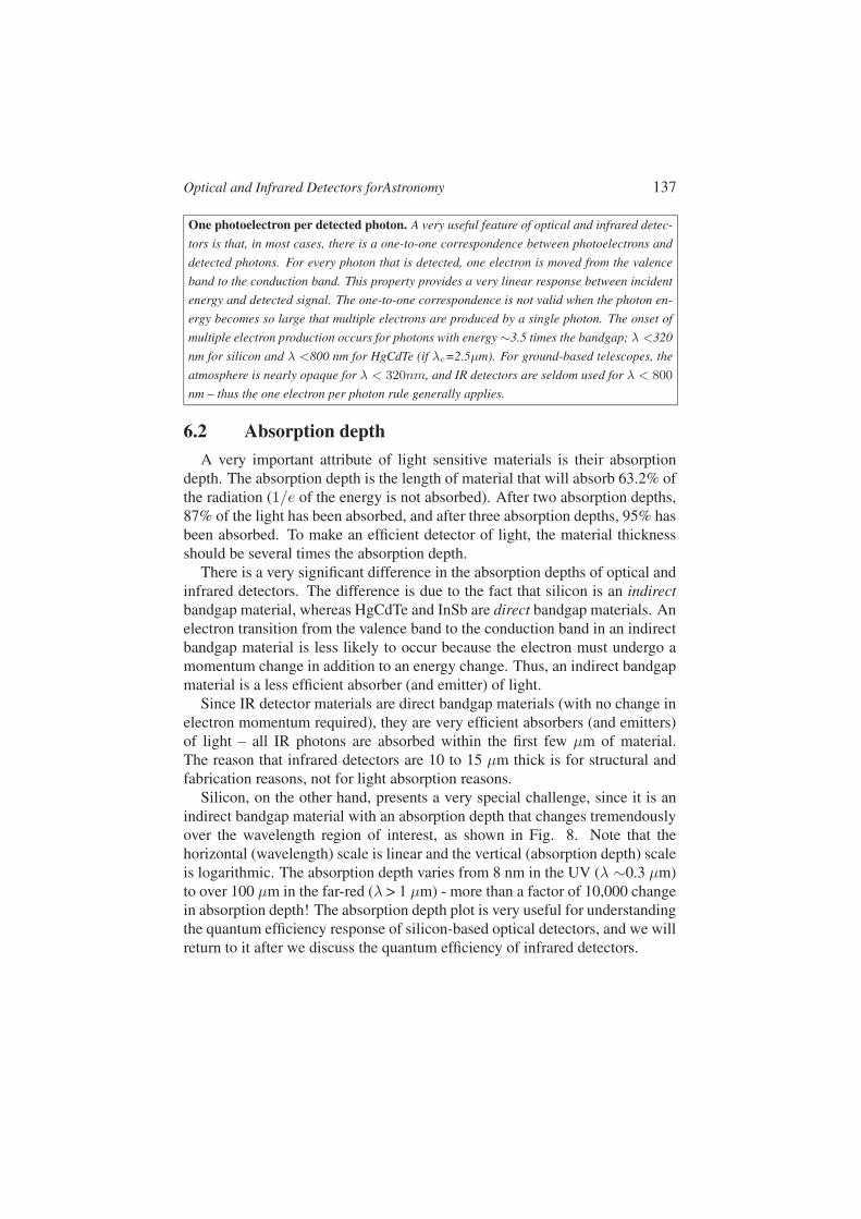
6.2 Absorption depthA very important attribute of light sensitive materials is their absorption
depth. The absorption depth is the length of material that will absorb 63.2% ofthe radiation (1/e of the energy is not absorbed). After two absorption depths,87% of the light has been absorbed, and after three absorption depths, 95% hasbeen absorbed. To make an efficient detector of light, the material thicknessshould be several times the absorption depth.There is a very significant difference in the absorption depths of optical and
infrared detectors. The difference is due to the fact that silicon is an indirectbandgap material, whereas HgCdTe and InSb are direct bandgap materials. Anelectron transition from the valence band to the conduction band in an indirectbandgap material is less likely to occur because the electron must undergo amomentum change in addition to an energy change. Thus, an indirect bandgapmaterial is a less efficient absorber (and emitter) of light.Since IR detector materials are direct bandgap materials (with no change in
electron momentum required), they are very efficient absorbers (and emitters)of light – all IR photons are absorbed within the first few µm of material.The reason that infrared detectors are 10 to 15 µm thick is for structural andfabrication reasons, not for light absorption reasons.Silicon, on the other hand, presents a very special challenge, since it is an
indirect bandgap material with an absorption depth that changes tremendouslyover the wavelength region of interest, as shown in Fig. 8. Note that thehorizontal (wavelength) scale is linear and the vertical (absorption depth) scaleis logarithmic. The absorption depth varies from 8 nm in the UV (λ ∼0.3 µm)to over 100 µm in the far-red (λ > 1 µm) - more than a factor of 10,000 changein absorption depth! The absorption depth plot is very useful for understandingthe quantum efficiency response of silicon-based optical detectors, and we willreturn to it after we discuss the quantum efficiency of infrared detectors.
138 OPTICS IN ASTROPHYSICS
Figure 8. Absorption depth of photons in silicon. Notice the tremendous variation in penetra-tion depth, from 8 nm in the UV to more than 100 µm in the far-red.
6.3 Infrared detector quantum efficiencyAs shown in Table 2, an IR detector without an AR coating will reflect over
30% of the incident light. Several of the first generation IR focal plane arrayswere fabricated on a glass substrate and it was not possible to put an AR coatingbetween the glass and the detector material. There are many IR detectors beingused today in astronomy that are without AR coating and have about 60% peakQE. If a single layer AR coating is used, infrared detectors typically achieve80% QE, as shown in Fig. 9 for a Rockwell Scientific 2K×2K detector.Infrared detectors can be made with several layer AR coatings, and the de-
tectors for the James Webb Space Telescope, awarded to Rockwell Scientific,specify 4- or 5-layer coatings to achieve QE of 95% over a broad bandpass.
6.4 Optical detector quantum efficiencyIn comparison to infrared detectors, it is much more difficult for silicon-
based optical detectors to achieve high QE over a wide bandpass. The mainchallenge is the tremendous variation of absorption depth shown in Fig. 8. Inaddition, the index of refraction varies significantly for λ = 0.32–1.1 µm, asshown in Fig. 10, making it difficult to optimize anti-reflection coatings forbroad bandpass.
Optical and Infrared Detectors forAstronomy 139
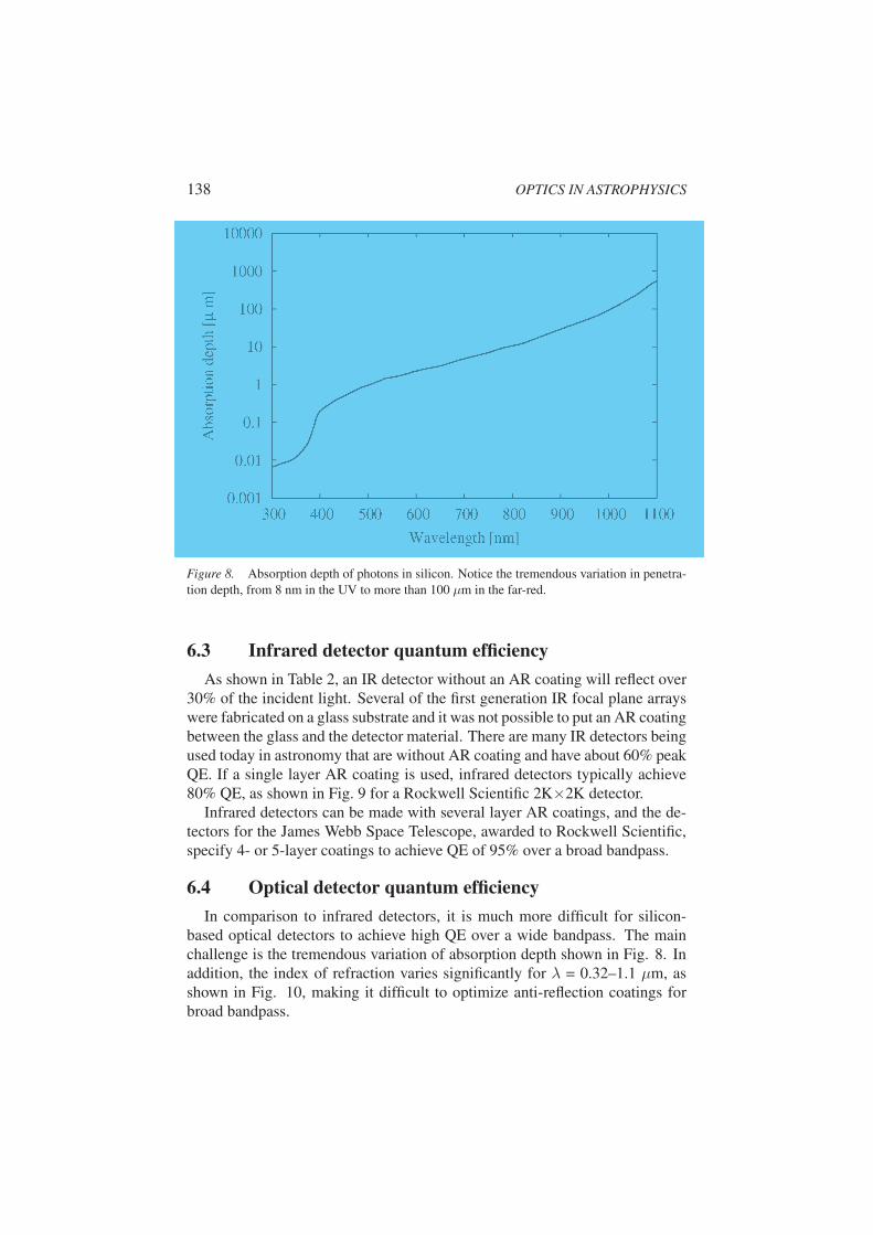
Figure 9. Quantum efficiency of a Rockwell 2K×2K HAWAII array. The atmospheric win-dows of J, H, and K are shown. Note the relatively constant QE across the 1-2.5 µm wavelengthregion, with peak QE of 84% in the K-band (centered at 2.2 µm). Figure courtesy of J. Garnett,Rockwell Scientific.
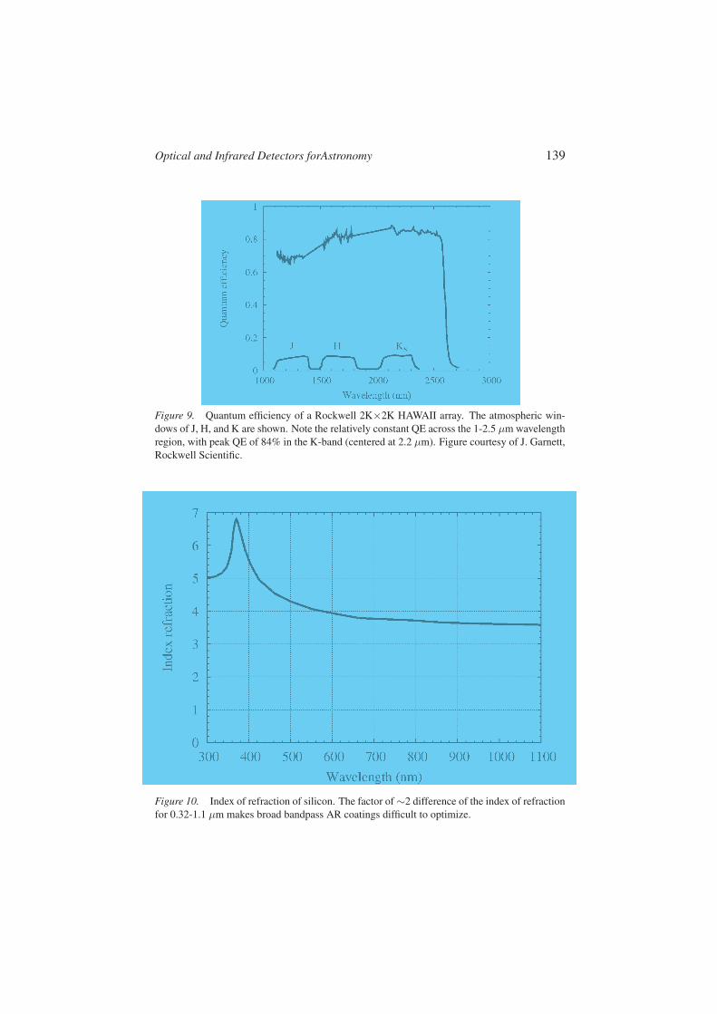
Figure 10. Index of refraction of silicon. The factor of∼2 difference of the index of refractionfor 0.32-1.1 µm makes broad bandpass AR coatings difficult to optimize.
140 OPTICS IN ASTROPHYSICS
The short penetration depth of UV/blue photons is the reason that “frontside”CCD detectors have very poor QE at the blue end of the spectrum. Thefrontside of a CCD is the side upon which the polysilicon wires that controlcharge collection and transfer are deposited. These wires are 0.25 to 0.5 µmthick and will absorb all UV/blue photons before these photons reach the pho-tosensitive volume of the CCD. For good UV/blue sensitivity, a silicon detectormust allow the direct penetration of photons into the photosensitive volume.This is achieved by turning the CCD over and thinning the backside until thephotosensitive region (the epitaxial layer) is exposed to incoming radiation.A thinned CCD will naturally build up an internal electric field that will pull
electrons to the back surface with a subsequent loss of photoelectrons. In orderto overcome this natural electric field, a backside passivation process must beused. There are three primary technologies to passivate the backside:
1 Boron implant with laser anneal. Boron atoms are accelerated into thebackside of the CCD, replacing about 1 of 10,000 silicon atoms witha boron atom. The boron atoms create a net negative charge that pushphotoelectrons to the front surface. However, the boron implant createsdefects in the lattice structure, so a laser is used to melt a thin layer (100nm) of the silicon. As the silicon resolidifies, the crystal structure re-turns with some boron atoms in place of silicon atoms. This works well,except for blue/UV photons whose penetration depth is shorter than thedepth of the boron implant. Variations in implant depth cause spatial QEvariations, which can be seen in narrow bandpass, blue/UV, flat fields.This process is used by E2V, MIT/LL and Sarnoff.2 Special coatings applied to the CCD backside. This process was pione-ered by the Jet Propulsion Laboratory (JPL) and has been significantlyimproved by Mike Lesser and his colleagues at the University of Ari-zona. A thin layer of transparent material is applied to the backside ofthe thinned CCD - this layer takes on a negative charge. Since the siliconis undisturbed and the negative charge layer is outside the silicon, thisapproach provides hiqh UV QE and very uniform flat field response inthe blue/UV. This process is now used by SITe, Fairchild and MIT/LL.3 MBE growth of very thin layer of boron and silicon. The problems asso-ciated with boron implant and laser anneal can be overcome by growinga very thin (5 nm) layer of silicon with boron atoms on the backside ofthe thinned CCD (1% boron, 99% silicon). The growth is applied bymolecular beam epitaxy (MBE) machines. This process was developedby JPL and MIT/LL.
The backside passivation processes are most critical for the blue and UVwavelengths. For 0.5-0.7 µm light, high QE is more easily attained - the ab-sorption depth is a few microns, and photons penetrate beyond the backside

Optical and Infrared Detectors forAstronomy 141
passivation layer, but do not pass all the way through the CCD. However, atthe red end of the optical spectrum, the photon can pass completely throughthe CCD - the absorption depths at 800, 900 and 1000 nm are 11, 29 and 94µm respectively.Combining the effects of index of refraction and penetration depth of pho-
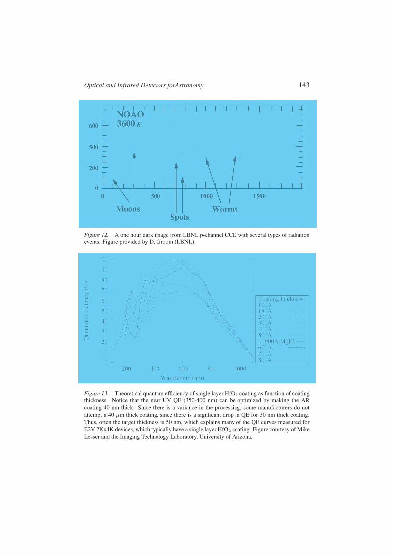
tons, the predicted CCD QE for a 15µm thick CCD with the “Lesser” backsidepassivation process and single layer HfO2 AR coating is presented in Fig.13.The sensitivity to thickness of AR coating and transparency of the CCD tolonger wavelengths is very evident.To provide high QE for λ = 0.75 − 1.1µm, the light sensitive silicon layer
must be made much thicker than the standard 15 µm thick CCD. The chal-lenge to producing a thicker device is finding a way to produce electric fieldsin the material that penetrate through most of the depth of the material to pro-duce good PSF. The two basic kinds of CCDs produced are n-channel andp-channel, depending on whether the CCD collects electrons or holes. MostCCDs are an n-channel devices.To produce a very thick n-channel device, the resistivity of the silicon must
be made relatively high, about 5,000 to 10,000 Ω-cm, as opposed to the 20-100 Ω-cm material used in “standard” n-channel CCDs. Higher resistivity isrequired for greater penetration depth of the fields produced by the frontsidepolysilicon wires (penetration depth is proportional to the square root of theresistivity). These “thick” high resistivity CCDs have been developed for de-tection of soft x-rays with space satellites and can be procured from E2V andMIT/LL.An example of the QE that can be obtained with the high resistivity n-
channel devices combined with the “Lesser” backside process is shown in Fig.11.The p-channel CCD has been developed by Steve Holland and his col-
leagues at Lawrence Berkeley National Laboratory (LBNL) to provide veryhigh QE in the far-red. (A parallel effort on p-channel CCD development isunderway at the Max-Planck Institut f -ur extraterrestische Physik under theleadership of Lothar Str-uder.) The LBNL p-channel devices are 300 µm thickwith 15 µm pixels, creating the interesting concept of a pixel “skyscraper”.The backside of the CCD (where photons enter) is coated with a thin layer(60 nm) of a transparent, conductive material (indium tin oxide, ITO) that ischarged to relatively high voltage (40 V). The backside charge produces a steepvoltage gradient in the device that pushes holes to the frontside and minimizescharge diffusion. Amazingly, the PSF of these devices is as good as 15 µmthick n-channel devices. The ITO layer also acts as one layer of a two-layerAR coating. Typically, LBNL uses 100 nm of silicon dioxide (Si02) as the sec-ond layer to optimize far-red QE: 90% QE has been achieved at 700-900 nmand 60% QE at 1000 nm. However, the very thick p-channel devices do suffer

142 OPTICS IN ASTROPHYSICS
Figure 11. Quantum efficiency of CCDs for the HIRES spectrograph on Keck I telescope.These CCDs will be highest QE devices ever mounted in an optical spectrograph. Three ofthese CCDs will be installed at the telescope in January 2004 and will make HIRES, onceagain, the most efficient high resolution spectrograph on the planet. The CCDs are all 45 µmthick, high resistivity n-channel devices produced by MIT/LL. The blue optimized CCDs (twoof them) have undergone backside processing at the University of Arizona, followed by singlelayer HfO2 AR coating tuned for maximum QE at 320 nm. The red optimized device has aboron implant / laser anneal treatment, with a two layer AR coating - SiO2 over HfO2. The QEcurves were measured by Richard Stover and Mingzhi Wei of Lick Observatory.
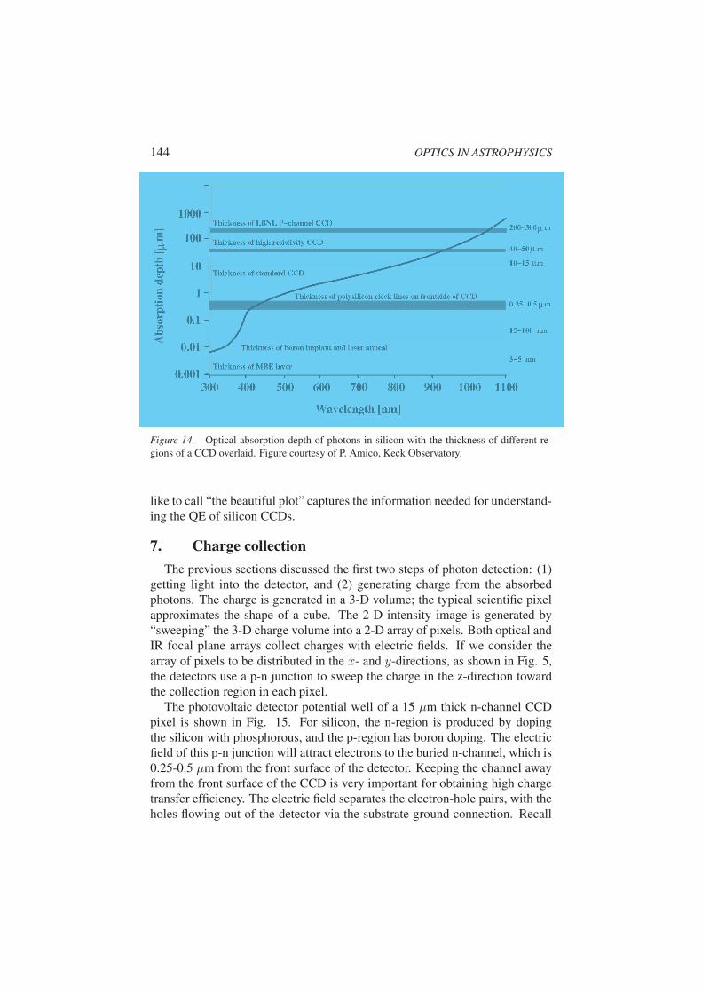
from one significant drawback. Due to their 300 µm thickness, the devices aregreat detectors of many types of radiation, including cosmic rays and radiationcreated by terrestrial sources. In fact, a dark image can look like images from aparticle physics experiment (see Fig. 12). Efforts are underway to find the bestway to shield the LBNL CCD from terrestrial radiation and to most efficientlyremove the unwanted radiation events from the data.The challenges of achieving high QE over the 0.3-1.1 µm band is summa-
rized in Fig. 14, which shows the optical absorption depth of photons in siliconwith the range of thickness of different regions of a CCD. Figure14, which welike to call “the beautiful plot” captures the information needed for understand-ing the QE of silicon CCDs.The challenges of achieving high QE over the 0.3-1.1 µm band is summa-
rized in Fig. 14, which shows the optical absorption depth of photons in siliconwith the range of thickness of different regions of a CCD. Figure14, which we
Optical and Infrared Detectors forAstronomy 143
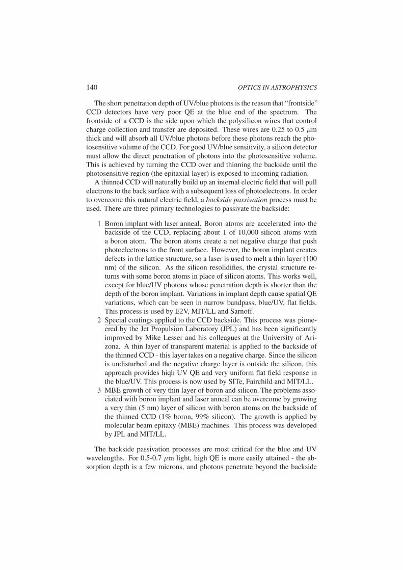
Figure 12. A one hour dark image from LBNL p-channel CCD with several types of radiationevents. Figure provided by D. Groom (LBNL).
Figure 13. Theoretical quantum efficiency of single layer HfO2 coating as function of coatingthickness. Notice that the near UV QE (350-400 nm) can be optimized by making the ARcoating 40 nm thick. Since there is a variance in the processing, some manufacturers do notattempt a 40 µm thick coating, since there is a signficant drop in QE for 30 nm thick coating.Thus, often the target thickness is 50 nm, which explains many of the QE curves measured forE2V 2Kx4K devices, which typically have a single layer HfO2 coating. Figure courtesy of MikeLesser and the Imaging Technology Laboratory, University of Arizona.
144 OPTICS IN ASTROPHYSICS
Figure 14. Optical absorption depth of photons in silicon with the thickness of different re-gions of a CCD overlaid. Figure courtesy of P. Amico, Keck Observatory.
like to call “the beautiful plot” captures the information needed for understand-ing the QE of silicon CCDs.
7. Charge collectionThe previous sections discussed the first two steps of photon detection: (1)
getting light into the detector, and (2) generating charge from the absorbedphotons. The charge is generated in a 3-D volume; the typical scientific pixelapproximates the shape of a cube. The 2-D intensity image is generated by“sweeping” the 3-D charge volume into a 2-D array of pixels. Both optical andIR focal plane arrays collect charges with electric fields. If we consider thearray of pixels to be distributed in the x- and y-directions, as shown in Fig. 5,the detectors use a p-n junction to sweep the charge in the z-direction towardthe collection region in each pixel.The photovoltaic detector potential well of a 15 µm thick n-channel CCD
pixel is shown in Fig. 15. For silicon, the n-region is produced by dopingthe silicon with phosphorous, and the p-region has boron doping. The electricfield of this p-n junction will attract electrons to the buried n-channel, which is0.25-0.5 µm from the front surface of the detector. Keeping the channel awayfrom the front surface of the CCD is very important for obtaining high chargetransfer efficiency. The electric field separates the electron-hole pairs, with theholes flowing out of the detector via the substrate ground connection. Recall

Optical and Infrared Detectors forAstronomy 145
Figure 15. Photovoltaic detector potential well. The example in this figure is the p-n junctionof a n-channel CCD. The x-y-z axes match the orientation shown in Fig. 5. The charge generatedin the 3-D volume of a pixel is swept toward a 2-D layer, which is the buried channel that is0.25-0.5 µm from the front surface of the detector. The z-direction potential is created by thep-n junction combined with the voltages on the polysilicon wires deposited on the frontside ofthe CCD (not shown in this figure).
that in a p-channel CCD, the internal electric fields collect holes instead ofelectrons.The p-n junction collapses the 3-D charge distribution into a 2-D array. The
pixel boundaries of the 2-D arrays are generated differently in optical and in-frared detector arrays.In CCDs, the boundaries in the column direction are defined permanently
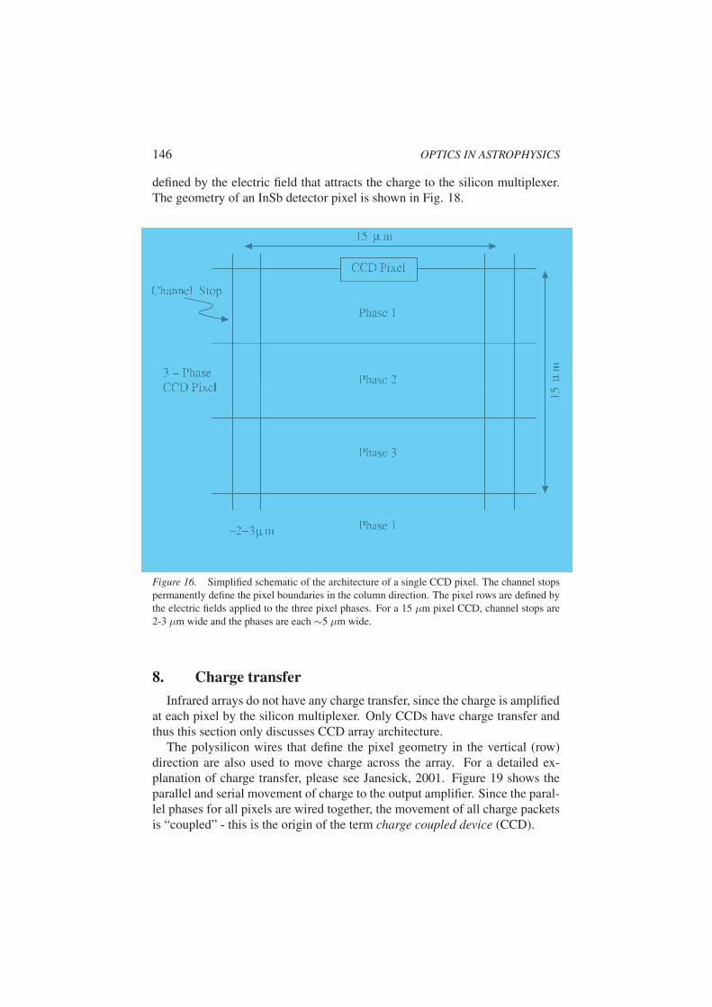
by doping the silicon. For an n-channel CCD, the channel stops are producedby boron doping; the 2-3 µm wide channel stop does not absorb photoelec-trons since the boron is only implanted a small distance (∼0.5 µm) into thefront surface. In the row direction, the pixels are defined by the electric fieldsof polysilicon wires that are fabricated on the front surface of the CCD. Thereare three parallel wires per pixel in a “three phase” CCD. During integration,two phases of the CCD are kept at a positive voltage to attract electrons, withthe third (barrier) phase biased at a negative voltage to provide a barrier be-tween the rows of the CCD. Figure 16 shows a simplified schematic of thearchitecture of a CCD pixel.In the infrared, the light sensitive material is bump bonded at each pixel to
a silicon multiplexer that amplifies the charge and multiplexes the outputs toexternal electronics, as shown in Fig. 17. The column and row boundaries are
146 OPTICS IN ASTROPHYSICS
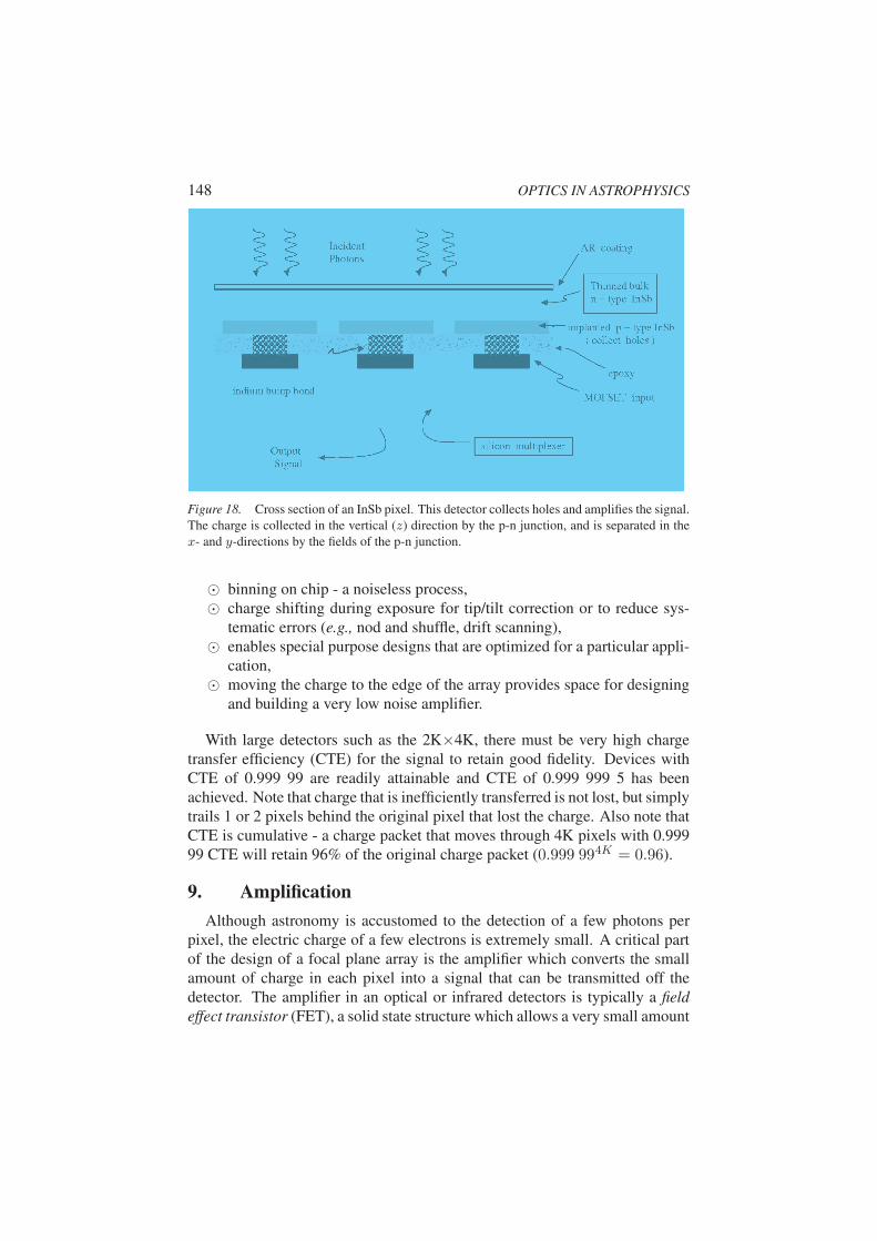
defined by the electric field that attracts the charge to the silicon multiplexer.The geometry of an InSb detector pixel is shown in Fig. 18.
Figure 16. Simplified schematic of the architecture of a single CCD pixel. The channel stopspermanently define the pixel boundaries in the column direction. The pixel rows are defined bythe electric fields applied to the three pixel phases. For a 15 µm pixel CCD, channel stops are2-3 µm wide and the phases are each ∼5 µm wide.
8. Charge transferInfrared arrays do not have any charge transfer, since the charge is amplified
at each pixel by the silicon multiplexer. Only CCDs have charge transfer andthus this section only discusses CCD array architecture.The polysilicon wires that define the pixel geometry in the vertical (row)
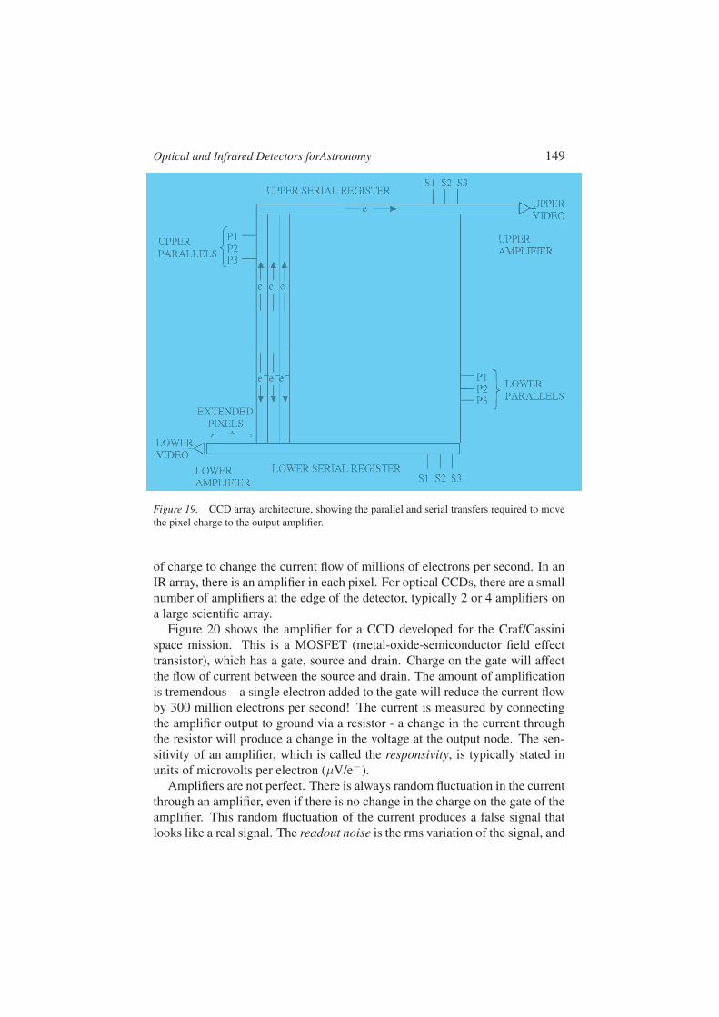
direction are also used to move charge across the array. For a detailed ex-planation of charge transfer, please see Janesick, 2001. Figure 19 shows theparallel and serial movement of charge to the output amplifier. Since the paral-lel phases for all pixels are wired together, the movement of all charge packetsis “coupled” - this is the origin of the term charge coupled device (CCD).

Optical and Infrared Detectors forAstronomy 147
Figure 17. Infrared array geometry. The light sensitive material is connected at each pixelby an indium bump bond to the silicon multiplexer that reads out the charge generated by theincident light. Figure courtesy of I. McLean (UCLA).
Charge transfer has both good and bad features. The negative aspects ofcharge transfer include:
⊗ takes time,⊗ can blur the image if a shutter is not used,⊗ can lose or blur the charge during the transfer (charge transfer inefficiency),⊗ allows a saturated pixel to bleed charge up and down a column,⊗ a trap in a pixel can block an entire column,⊗ a “hot” pixel defect can release charge into all pixels that are moved pastit during readout.
With proper design, fabrication and clocking, most of these negative aspectscan be overcome, but there are usually some bad columns due to blockedcolumns or hot pixels. There are many positive aspects of charge transfer,giving the CCD some very good and unique attributes vis-a-vis an infrareddetector:
148 OPTICS IN ASTROPHYSICS
Figure 18. Cross section of an InSb pixel. This detector collects holes and amplifies the signal.The charge is collected in the vertical (z) direction by the p-n junction, and is separated in thex- and y-directions by the fields of the p-n junction.
binning on chip - a noiseless process, charge shifting during exposure for tip/tilt correction or to reduce sys-tematic errors (e.g., nod and shuffle, drift scanning),
enables special purpose designs that are optimized for a particular appli-cation,
moving the charge to the edge of the array provides space for designingand building a very low noise amplifier.
With large detectors such as the 2K×4K, there must be very high chargetransfer efficiency (CTE) for the signal to retain good fidelity. Devices withCTE of 0.999 99 are readily attainable and CTE of 0.999 999 5 has beenachieved. Note that charge that is inefficiently transferred is not lost, but simplytrails 1 or 2 pixels behind the original pixel that lost the charge. Also note thatCTE is cumulative - a charge packet that moves through 4K pixels with 0.99999 CTE will retain 96% of the original charge packet (0.999 994K = 0.96).
9. AmplificationAlthough astronomy is accustomed to the detection of a few photons per
pixel, the electric charge of a few electrons is extremely small. A critical partof the design of a focal plane array is the amplifier which converts the smallamount of charge in each pixel into a signal that can be transmitted off thedetector. The amplifier in an optical or infrared detectors is typically a fieldeffect transistor (FET), a solid state structure which allows a very small amount
Optical and Infrared Detectors forAstronomy 149
Figure 19. CCD array architecture, showing the parallel and serial transfers required to movethe pixel charge to the output amplifier.
of charge to change the current flow of millions of electrons per second. In anIR array, there is an amplifier in each pixel. For optical CCDs, there are a smallnumber of amplifiers at the edge of the detector, typically 2 or 4 amplifiers ona large scientific array.Figure 20 shows the amplifier for a CCD developed for the Craf/Cassini
space mission. This is a MOSFET (metal-oxide-semiconductor field effecttransistor), which has a gate, source and drain. Charge on the gate will affectthe flow of current between the source and drain. The amount of amplificationis tremendous – a single electron added to the gate will reduce the current flowby 300 million electrons per second! The current is measured by connectingthe amplifier output to ground via a resistor - a change in the current throughthe resistor will produce a change in the voltage at the output node. The sen-sitivity of an amplifier, which is called the responsivity, is typically stated inunits of microvolts per electron (µV/e−).Amplifiers are not perfect. There is always random fluctuation in the current
through an amplifier, even if there is no change in the charge on the gate of theamplifier. This random fluctuation of the current produces a false signal thatlooks like a real signal. The readout noise is the rms variation of the signal, and

150 OPTICS IN ASTROPHYSICS
Figure 20. Example of CCD MOSFET amplifier - Craf/Cassini design. This is a high resolu-tion image of the fronside of a n-channel CCD - note the 40 µm scale shown on the right. Onlythe portion of the CCD near the output amplifier is shown. In the photograph on the left, a smallportion of the image array is seen. The operation of the pixel readout is as follows. The chargefrom each pixel is moved to the output amplifier through the serial register. Multiple pixels canbe binned in the serial direction at the summing well. When a pixel is read out, the output gateis first set to the reset voltage by the reset transistor which is controlled by the reset clock. Fora typical CCD, the reset voltage is about 9 volts, which “turns on” the current flowing betweensource and drain in the MOSFET. After the reset gate is open and closed, the charge in the sum-ming well is pushed over the “wall” of the output gate by clocking the summing well positive(high enough voltage to push charge over the output gate, but not so high as to push charge backup the serial register). The charge on the output gate affects the current from source to drain -with more electron charge on the gate there is less current between source and drain. The lineardynamic range of a typical CCD MOSFET is 2 volts - a high responsivity (20 µV/e−) amplifierwill saturate at about 100,000 electrons. Figure courtesy of J. Janesick
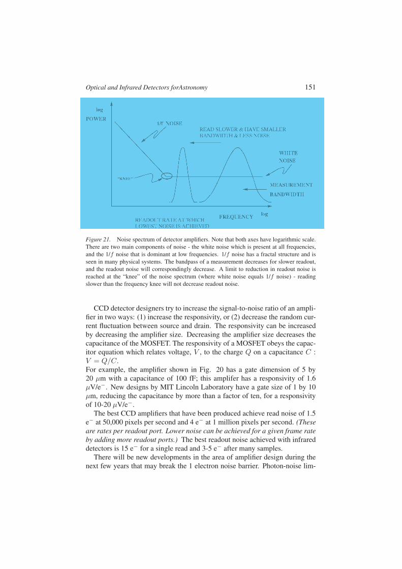
is stated in units of electrons at the gate of the amplifier. The noise spectrumof a FET, shown in Fig. 21, has two components, a white noise componentand a 1/f noise component. By reading out slower, the random white noisefluctuations can be averaged, and lower noise achieved, until the 1/f noisebecomes dominant. Since a CCD places the amplifiers at the edge of the array,there is room to design and place a very low noise amplifier. The amplifiersin IR arrays have less room and more signals in close vicinity, and thus IRamplifiers typically have higher noise.The CCD MOSFET is a destructive readout device - there is only one mea-
surement per charge packet. However, an infrared amplifier can be read outseveral times, with averaging and corresponding reduction in the effectivereadout noise (16 reads can reduce the noise by a factor of
√16 or 4). In
theory, multiple readout of an infrared amplifier could achieve extremely lownoise, but in practice, due to other complications, the noise reduction usuallyreaches a limit of 4-5 improvement (achieved after 16-32 reads).
Optical and Infrared Detectors forAstronomy 151
Figure 21. Noise spectrum of detector amplifiers. Note that both axes have logarithmic scale.There are two main components of noise - the white noise which is present at all frequencies,and the 1/f noise that is dominant at low frequencies. 1/f noise has a fractal structure and isseen in many physical systems. The bandpass of a measurement decreases for slower readout,and the readout noise will correspondingly decrease. A limit to reduction in readout noise isreached at the “knee” of the noise spectrum (where white noise equals 1/f noise) - readingslower than the frequency knee will not decrease readout noise.
CCD detector designers try to increase the signal-to-noise ratio of an ampli-fier in two ways: (1) increase the responsivity, or (2) decrease the random cur-rent fluctuation between source and drain. The responsivity can be increasedby decreasing the amplifier size. Decreasing the amplifier size decreases thecapacitance of the MOSFET. The responsivity of a MOSFET obeys the capac-itor equation which relates voltage, V , to the charge Q on a capacitance C :V = Q/C.For example, the amplifier shown in Fig. 20 has a gate dimension of 5 by20 µm with a capacitance of 100 fF; this amplifer has a responsivity of 1.6µV/e−. New designs by MIT Lincoln Laboratory have a gate size of 1 by 10µm, reducing the capacitance by more than a factor of ten, for a responsivityof 10-20 µV/e−.The best CCD amplifiers that have been produced achieve read noise of 1.5
e− at 50,000 pixels per second and 4 e− at 1 million pixels per second. (Theseare rates per readout port. Lower noise can be achieved for a given frame rateby adding more readout ports.) The best readout noise achieved with infrareddetectors is 15 e− for a single read and 3-5 e− after many samples.There will be new developments in the area of amplifier design during the
next few years that may break the 1 electron noise barrier. Photon-noise lim-
152 OPTICS IN ASTROPHYSICS
ited performance at all light levels may truly be “just around the corner” (GuyMonnet, European Southern Observatory - 1999).
10. SummaryThis chapter has shown the importance of detectors in the astronomical en-
terprise and the role that they fill in an astronomical observatory. The physicsand operation of optical and infrared detectors for ground-based telescopeswas presented. The detection of light was shown to consist of five steps: (1)getting light into the detector, (2) charge generation, (3) charge collection, (4)charge transfer (only in CCDs, not in IR), and (5) charge amplification. Thesesteps were explained for optical and infrared detectors and the state-of-the-artperformance was presented throughout the text. Optical and infrared detec-tors have achieved a high level of performance and will continue to serve asthe “eyes” of astronomy, allowing humankind to explore the cosmos on evergrander scales.
ReferencesEvery three years, representatives of all of the major observatories and everydetector manufacturer gather to exchange information on the state-of-theart. The proceedings from the past two workshops, held in 2002 (Hawaii)and 1999 (Germany), capture the most recent developments in optical andinfrared detectors:
P. Amico and J. W. Beletic eds., 2003, Scientific Detectors for Astronomy 2002,the beginning of a new era, ASSL Series, Kluwer Academic Publisher, Dor-drecht
P. Amico and J. W. Beletic eds., Optical Detectors for Astronomy II, state-of-the-art at the turn of the millenium, ASSL Series, Kluwer Academic Pub-lisher, Dordrecht, 2000.
James Janesick has been the most influential person in CCD community formany years, not only making significant technological developments, butalso playing the role of lead evangelist. His classic “CCD course”, held bi-annually at UCLA, is a pilgrimage many of us in the field have made. Hehas finally captured all of his lecture notes into one tomb.
J. R. Janesick, 2001, Scientific Charge-Coupled Devices, SPIE Press, Belling-ham
For an excellent overview of all aspects of astronomical instrumentation, pleasesee the classic textbook by Ian McLean. This book contains a very goodpedantic explanation of optical and infrared detectors.
I. S. McLean, 1997, Electronic Imaging in Astronomy: Detectors and Instru-mentation, John Wiley and Sons, Chichester
Optical and Infrared Detectors forAstronomy 153
All of the optical and infrared focal plane arrays are solid state electronic de-vices, and to fully understand their physics and operation, one should havea solid foundation in the solid state electronics. An excellent reference is:
B. G. Streetman, 1990, Solid State Electronic Devices, Prentice-Hall, Engle-wood Cliffs

154 OPTICS IN ASTROPHYSICS


![arXiv:1203.3816v1 [astro-ph.IM] 16 Mar 2012web.ipac.caltech.edu/staff/fmasci/home/astro_refs/... · By providing a variety of statistical algorithms for all phases of the inference](https://static.fdocuments.us/doc/165x107/5f08a2827e708231d422fa88/arxiv12033816v1-astro-phim-16-mar-by-providing-a-variety-of-statistical-algorithms.jpg)

