Optical and Electronic Studies of Photostability and ...
148
Optical and Electronic Studies of Photostability and Charge Dynamics By Yi Zheng Tan A dissertation submitted in partial fulfillment of the requirements for the degree of Doctor of Philosophy (Chemistry) at the UNIVERSITY OF WISCONSIN-MADISON 2013 Date of final oral examination: 06/20/13 The dissertation is approved by the following members of the Final Oral Committee: Robert J. Hamers, Professor, Chemistry John C. Wright, Professor, Chemistry Song Jin, Associate Professor, Chemistry Randall H. Goldsmith, Assistant Professor, Chemistry Joel A. Pedersen, Professor, Soil Science
Transcript of Optical and Electronic Studies of Photostability and ...

Optical and Electronic Studies of Photostability and Charge Dynamics
By
Yi Zheng Tan
A dissertation submitted in partial fulfillment of
the requirements for the degree of
Doctor of Philosophy
(Chemistry)
at the
UNIVERSITY OF WISCONSIN-MADISON
2013
Date of final oral examination: 06/20/13
The dissertation is approved by the following members of the Final Oral Committee: Robert J. Hamers, Professor, Chemistry John C. Wright, Professor, Chemistry Song Jin, Associate Professor, Chemistry Randall H. Goldsmith, Assistant Professor, Chemistry Joel A. Pedersen, Professor, Soil Science

i
Optical and Electronic Studies of Photostability and Charge Dynamics
Yi Zheng Tan
Under the supervision of Professor Robert J. Hamers
University of Wisconsin-Madison
Abstract
This thesis encompasses three areas of research:
(1) Ligand chemistry for enhanced photostability of CdSe quantum dots (QDs): Chalcogenide quantum
dots such as CdSe and PbSe have potential as absorbers for QD-sensitized solar cells, but their
practical utility is limited by fast degradation when exposed to ambient environments. Our work
explored how the molecular structure of small thiol ligands affects the photostability of CdSe QDs.
We found that electron donating conjugated ligands enhanced the photostability by effectively
trapping oxidative holes from the QD. To further this chemistry, we developed an in-situ
functionalization method of conjugated dithiocarbamates on CdSe/TiO2, and explored the para-
substituent effect of these conjugated ligands on the photostability of CdSe.
(2) Spectroelectrochemistry of the iodide-triiodide redox couple: Alternatives to the standard Pt
counter electrode to the dye-sensitized solar cells are conducting polymers and carbon
nanomaterials. To try to understand differences in their mechanisms, we discuss our efforts with a
home-built spectroelectrochemical cell to enable spectral measurement of changes in the iodine
species with a voltage sweep.
(3) Surface photovoltage (SPV) measurement for charge dynamics of materials: SPV measurement is a
contactless technique to characterize semiconductor surfaces. We developed a transient-SPV
measurement to directly measure fast charge transfer processes that uses ns-pulsed excitations
onto a capacitive coupled sample. To resolve dynamics faster dynamics down to the fs-timescale, we

ii developed an SPV measurement technique using delayed ultrafast laser pulses. The non-linear
behaviour of SPV allows time-averaged electronic measurements. With this technique, we
successfully measured nanosecond to picosecond relaxation dynamics of a few highly doped
semiconductors. We further tracked changes in carrier dynamics of natural pyrite after various
surface treatments.

iii
Acknowledgements
It has been a long 6 years, and I am grateful to so many people for their help and support.
First and foremost, I would like to thank my advisor, Bob Hamers for his guidance and support
throughout my years here. Bob, your enthusiasm and optimism for science has been a constant source
of motivation and inspiration, especially when things were not going as well as I had hoped. I am very
grateful to the Hamers group, past and present, for the mentorship, the friendship, and overall for being
a supportive and nurturing academic family. I would like to especially thank my officemates and
labmates, Jeremy, Drew, Bo, Mike, Michelle, Courtney, Lee, Caroline, Marco, Linghong, and Arielle for
making the workplace not only a productive but also a fun and exciting environment. Mike, you are
much missed. Marco, thanks to you, I will eternally be the ‘Chef’ of the ‘Hamers Group Muppets’. I am
also grateful to group members who started with me at the same time, Kacie, Xin, and Rose. Your
company has made my graduate school life less stressful.
I have been very fortunate to be involved in collaborations outside my group. I am grateful to
Song Jin and John Wright for helpful discussions and suggestions to improve my research. A large part of
my research has been highly collaborative between the Jin and Wright groups, so I tremendously
appreciate my collaborators from these two groups, especially Skye, Andrei, Miguel, Dan, Blaise, Qi, and
Kyle for your contributions to my projects. I am happy to have helped your research in some way too,
however minor.
Finally, I am grateful to my family and friends. I would like to thank my old college friends,
especially John. Even though we have parted ways since our undergraduate days, you have kept our
friendship going strong. Jon, without you, I do not think I would have made it this far in graduate school.
Thank you for all your love and support.
iv
Table of Contents
Abstract .......................................................................................................................................................... i
Acknowledgments ........................................................................................................................................ iii
Table of Contents ......................................................................................................................................... iv
Chapter 1 Introduction and Background ..................................................................................................... 1
1.1 The Advent of Dye Sensitized Solar Cells ............................................................................................ 1
1.2 The Iodide-Triiodide Redox Couple and Counter Electrode ............................................................... 2
1.3 Inorganic Nanocrystals as Potential Absorbers for Sensitized Solar Cells .......................................... 4
1.4 The Issue of Quantum Dot Stability .................................................................................................... 7
1.5 Surface Photovoltage Spectroscopy for Measurements of Charge Transfer and Charge Dynamics
................................................................................................................................................................. 10
1.6 Scope of Thesis .................................................................................................................................. 13
1.7 References......................................................................................................................................... 14
Chapter 2 Influence of Hole-Sequestering Ligands on the Photostability of CdSe Quantum Dots ........... 19
2.1 Introduction ...................................................................................................................................... 19
2.2 Experimental ..................................................................................................................................... 21
2.2.1 Chemicals .............................................................................................................................. 21
2.2.2 Preparation of Nanocrystalline TiO2 Films ............................................................................ 21
2.2.3 Synthesis of CdSe QDs .......................................................................................................... 22
2.2.4 CdSe-TiO2 Adduct Formation and Subsequent Ligand Exchange ......................................... 22
2.2.5 Fourier Transform Infrared (FTIR) Spectroscopy .................................................................. 23
2.2.6 X-ray Photoelectron Spectroscopy (XPS) .............................................................................. 23
2.2.7 Photodegradation Studies .................................................................................................... 23
v 2.2.8 Photoluminescence ............................................................................................................... 24
2.2.9 Density Functional Theory (DFT) Calculations ...................................................................... 24
2.2.10 Fabrication of CdSe Sensitized TiO2 Solar Cells ................................................................... 25
2.3 Results ............................................................................................................................................... 25
2.3.1 FTIR Characterization of Functionalized CdSe/TiO2 Surfaces ............................................... 25
2.3.2 Photostability in Water ......................................................................................................... 27
2.3.3 Comparison of Molecular Coverages .................................................................................... 31
2.3.4 Photostability in Air............................................................................................................... 31
2.3.5 Photoluminescence ............................................................................................................... 33
2.3.6 DFT Calculations .................................................................................................................... 35
2.4 Discussion .......................................................................................................................................... 36
2.5 Effect of DMATP in a Liquid Junction Solar Cell ................................................................................ 40
2.6 Extending the DMATP Passivation Method to PbS and PbSe QDs ................................................... 42
2.7 Conclusions ....................................................................................................................................... 42
2.8 References......................................................................................................................................... 43
Chapter 3 Photostability of CdSe Quantum Dots Functionalized with Small Conjugated Dithiocarbamates
(DTCs) .......................................................................................................................................................... 50
3.1 Introduction ...................................................................................................................................... 50
3.2 Experimental ..................................................................................................................................... 51
3.2.1 Chemicals .............................................................................................................................. 51
3.2.2 Preparation of Nanocrystalline TiO2 Films ............................................................................ 51
3.2.3 Synthesis of CdSe QDs .......................................................................................................... 52
3.2.4 CdSe-TiO2 Preparation and Ligand Modification .................................................................. 52
3.2.5 Fourier Transform Infrared (FTIR) Spectroscopy .................................................................. 53

vi 3.2.6 X-ray Photoelectron Spectroscopy (XPS) .............................................................................. 53
3.2.7 Water Photostability Studies ................................................................................................ 53
3.2.8 Photoluminescence (PL) ....................................................................................................... 54
3.3 Results ............................................................................................................................................... 54
2.3.1 FTIR and XPS Characterization .............................................................................................. 54
2.3.2 Water Photostability of R-Ph-DTC Functionalized CdSe-TiO2 ............................................... 60
2.3.3 Photoluminescence ............................................................................................................... 62
2.3.4 Photostability of DTC vs. Thiol Bound CdSe-TiO2 Surfaces ................................................... 64
3.4 Discussion .......................................................................................................................................... 66
3.5 Conclusions ....................................................................................................................................... 68
3.6 References......................................................................................................................................... 68
Chapter 4 Spectroelectrochemistry of the Iodide-Triiodide Redox Couple ............................................... 73
4.1 Introduction ...................................................................................................................................... 73
4.2 Mechanism of Electrochemical Reactions of the Iodide-Triiodide Redox Couple on Platinum ....... 74
4.3 Experimental ..................................................................................................................................... 75
4.3.1 Materials ............................................................................................................................... 75
4.3.2 Electrochemistry ................................................................................................................... 75
4.3.3 Spectroelectrochemistry ....................................................................................................... 76
4.4 Results and Discussion ...................................................................................................................... 76
4.4.1 Absorption Spectra of Iodine Species ................................................................................... 76
4.4.2 Electrochemistry of the Iodide-Triiodide Couple on Pt and PEDOT-PSS .............................. 78
4.4.3 Spectroelectrochemistry ....................................................................................................... 79
4.5 Conclusions ....................................................................................................................................... 83
4.6 References......................................................................................................................................... 83
vii Chapter 5 Surface Photovoltage Techniques for Measurements of Charge Transfer and Charge Dynamics
.................................................................................................................................................................... 86
5.1 Introduction ...................................................................................................................................... 86
5.2 SPV Cell Setup ................................................................................................................................... 87
5.3 Steady-State SPV Experiments .......................................................................................................... 89
5.4 Transient SPV Experiments ............................................................................................................... 91
5.5 Ultrafast SPV Experiments ................................................................................................................ 99
5.6 Conclusions ..................................................................................................................................... 103
5.7 References....................................................................................................................................... 105
Chapter 6 Conclusions and Outlook.......................................................................................................... 107
Appendix ................................................................................................................................................... 109
A1 Molecular Coverage Calculations from XPS Data for Ligands on Nanoparticles ............................. 109
A2 Technical Design and Drawing of the Spectroelectrochemistry Cell ............................................... 115
A3 Technical Design and Drawing of the SPV Cell ................................................................................ 118
A4 Additional Data on Surface Photovoltage (SPV) Measurement ...................................................... 119
A4.1 Steady-State SPV Measurement .......................................................................................... 119
A4.1.1 CdSe Quantum Dot (QD) Functionalized on Doped Single Crystal Rutile (SCR) TiO2
(110) ................................................................................................................................ 119
A4.2 Transient SPV Measurement ............................................................................................... 121
A4.2.1 Bulk Diamond ...................................................................................................... 121
A4.2.2 N719 Dye on Porous Nanocrystalline TiO2 Films ................................................. 125
A4.2.3 TiO2 (Single Crystal Rutile) ................................................................................... 126
A4.2.4 ZnO (Single Crystal Sample and Porous Nanocrystalline Film) ............................ 128
A4.2.5 Iron Pyrite (FeS2) .................................................................................................. 130

viii A4.2.6 Layered Chalcogenide Nanostructures of MoS2, WS2, and WSe2 ....................... 132
A4.2.7 Sensitized SnO2 ................................................................................................... 133
A4.2.8 Hematite (α-Fe2O3) Nanowires on FTO ............................................................... 134
A4.3 Ultrafast SPV ........................................................................................................................ 135
A4.3.1 Ultrafast SPV of n-GaAs ....................................................................................... 135
A4.3.2 Ultrafast SPV of Synthetic Single Crystal Iron Pyrite ........................................... 137
A4.4 References ........................................................................................................................... 138
1
Chapter 1
Introduction and Background
1.1 The Advent of Dye Sensitized Solar Cells
Energy from the sun is the one of the most viable clean, renewable resources to meet our
increasing world energy demand. We can convert sunlight directly into electricity with photovoltaic
cells. Current cells that are widely used are Si wafer-based p/n junctions. For these cells, defects in the Si
wafer crystals increase the recombination rates of electrons and holes, so high efficiency relies on
having highly crystalline materials, which are expensive to manufacture. To lower cost, there has been
some success with the so-called ‘second generation solar cells’ in which thin films are used instead of
wafers, with materials such as cadmium telluride, copper indium gallium selenide (CIGS), and gallium
arsenide.1 However, they still suffer from cost issues (exotic materials such as indium are rare and
expensive), and also potential toxicity from the use of cadmium.
In 1991, O’Regan and Grätzel demonstrated the success of a dye-sensitized solar cell (DSSC) as
another low-cost alternative in the family of second generation solar cells.2 Sensitization is a way to
enhance the generation of photocurrent obtained from a semiconductor electrode by introducing an
absorber (traditionally a metal-complex dye) that can absorb light at longer wavelengths and transfer
photo-excited charges into the semiconductor.3 Before the work of O’Regan and Grätzel, sensitized
systems have been studied for potential light harvesting applications but suffered from very low
efficiencies. These studies focused on flat surfaces, and therefore had the problem of low absorption by
the thin monolayer of sensitizer. O’Regan and Grätzel revolutionized the concept of this sensitized
system by introducing a porous network of interconnected nano-sized crystals of anatase TiO2 as the
electron acceptor, thus greatly increasing the surface area of the electrode. The high surface coverage of
the sensitizing dye makes the electrode highly absorptive, and subsequently can potentially generate
2 increased photocurrents. TiO2 is a stable, low cost semiconductor with a lot of potential in
photoelectrochemical applications, but its large bandgap (3.2 eV for anatase) does not ideally match the
solar spectrum. The dye, informally named N3, is a Ru-bipyridyl complex with two carboxylic acid groups
on each bipyridine ligand and has an absorption onset in the near IR region. The carboxylic acids serve as
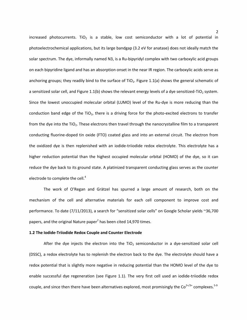
anchoring groups; they readily bind to the surface of TiO2. Figure 1.1(a) shows the general schematic of
a sensitized solar cell, and Figure 1.1(b) shows the relevant energy levels of a dye sensitized-TiO2 system.
Since the lowest unoccupied molecular orbital (LUMO) level of the Ru-dye is more reducing than the
conduction band edge of the TiO2, there is a driving force for the photo-excited electrons to transfer
from the dye into the TiO2. These electrons then travel through the nanocrystalline film to a transparent
conducting fluorine-doped tin oxide (FTO) coated glass and into an external circuit. The electron from
the oxidized dye is then replenished with an iodide-triiodide redox electrolyte. This electrolyte has a
higher reduction potential than the highest occupied molecular orbital (HOMO) of the dye, so it can
reduce the dye back to its ground state. A platinized transparent conducting glass serves as the counter
electrode to complete the cell.4
The work of O’Regan and Grätzel has spurred a large amount of research, both on the
mechanism of the cell and alternative materials for each cell component to improve cost and
performance. To date (7/11/2013), a search for “sensitized solar cells” on Google Scholar yields ~36,700
papers, and the original Nature paper2 has been cited 14,970 times.
1.2 The Iodide-Triiodide Redox Couple and Counter Electrode
After the dye injects the electron into the TiO2 semiconductor in a dye-sensitized solar cell
(DSSC), a redox electrolyte has to replenish the electron back to the dye. The electrolyte should have a
redox potential that is slightly more negative in reducing potential than the HOMO level of the dye to
enable successful dye regeneration (see Figure 1.1). The very first cell used an iodide-triiodide redox
couple, and since then there have been alternatives explored, most promisingly the Co2+/3+ complexes.5-9
3
Sensitizer-TiO2
Redox couple e-
Counter Pt/FTO
FTO
e-
e-e-
hν
e-
hν
CB
VB
S
S+
Eredox
TiO2
E
(a)
(b)
Figure 1.1: (a) General scheme of a sensitized solar cell (b)
Relevant energy levels involved in electron transfer of a cell
4 Yet the majority of successful cells are the ones that utilized the iodide-triiodide couple. The
effectiveness is understood to be due to the nature of the oxidation-reduction kinetics of this redox
couple. Oxidation of the iodide to triiodide by the dye is kinetically much faster than its back reduction.9-
13 Thus, once the electrons are injected into the TiO2, recombination of these electrons back to the
triiodide is inhibited.
The counter electrode in a DSSC functions to complete the cell by regenerating the oxidized
electrolyte triiodide species back to iodide. On this side of the cell, a fast reduction of triiodide to iodide
is desirable. The conventional counter electrode used is a platinized electrode, since Pt catalyzes
triiodide reduction. However, for reasons of cost and availability, this material is not ideal if we want to
make DSSCs economical for practical commercialization. Alternatives have been widely explored with
moderate success, including organic conducting polymers,14-16 carbon nanomaterials,17,18 various metal
oxides,19-21 sulfides,22,23 nitrides,21,24 and carbides.21,25 This shows the potential of further lowering the
cost of DSSCs, making their use more attractive.
1.3 Inorganic Nanocrystals as Potential Absorbers for Sensitized Solar Cells
In the first demonstration of the DSSC by O’Regan and Grätzel, they used a Ru-bipyridyl dye (N3)
as the absorber.2 Since then, there has been a great deal of effort in finding alternative sensitizers either
to extend the dye absorption deeper into the near IR and/or to lower the cost. Although only a thin layer
of dye is needed per photovoltaic cell, Ru metal is expensive and its cost could be prohibitive for
practical commercialization.26 A large research area that has branched out of the DSSC is the use of
inorganic semiconducting nanocrystals as the potential sensitizer.27
Nanocrystals (crystalline particles with length scales of 1 – 100 nm) have unique physical and
electronic properties that differ from their macro-sized bulk counterparts due to their small sizes.
Among them are quantum dots (QDs), semiconducting nanocrystals with sizes comparable or smaller
than their exciton Bohr radii, leading to quantum confinement in all directions. The Bohr radius depends

5 on the nature of the crystal lattice structure, so this quantity differs for each semiconducting material.
The physical confinement results in electronic properties that are in between small isolated molecules
and large macro-sized crystals, as illustrated in Figure 1.2(a). In an isolated molecule, electronic energy
levels are discrete; we commonly describe these levels with molecular orbitals, HOMOs and LUMOs. On
the other end, bulk crystalline semiconductors have continuous energy levels that form bands; the filled
band is termed the valence band (VB), while the empty band is the conduction band (CB), and the
minimum energy to excite an electron from the VB into the CB is the band gap (Eg). As we decrease the
size of semiconductor crystals to below the exciton radius, the energy of its charge carriers increases
due to the increased spatial confinement, and the electronic band structure becomes discretized,
resembling more like an isolated molecule. The bandgap in a QD becomes larger than that of the bulk.
Due to the spatial nature of the quantum confinement, the resulting electronic structure is highly shape
and size dependent. Smaller QDs have stronger confinement effects, and therefore larger bandgaps.28
Since we can tune the electronic properties of these nanocrystals with size and shape, one of the
advantages in using them as sensitizing absorbers is the opportunity to optimize the bandgap of the
nanocrystal to ideally match the solar spectrum.
Various nanocrystal materials have been studied as sensitizers, more popularly the
chalcogenides like CdS, CdSe, PbS, and PbSe. They have been paired with a number of wide band gap
semiconductors such as TiO2, SnO2, and ZnO to act as electron acceptors for sensitized solar cells.27 Since
the physical sizes and the electronic energies of semiconducting nanocrystals are intimately connected,
there is some bandgap engineering that needs to be considered. Figure 1.2(b), adapted from Tvrdy et.
al.,29 shows the energy alignments of a series of CdSe QD sizes to the bulk band energies of a few
electron acceptor materials. CdSe (Bohr radius = 5.4 nm),30 due to the position of its CB edge in the bulk,
is able to inject electrons into the CB of all of the electron acceptors shown in Figure 1.2(b) at all QD
sizes. The variation in QD size and electron acceptor material, however, changes the thermodynamic

6
(a)
(b)
(c)
nanocrystal
diameter (nm)
Figure 1.2: (a) Energy diagram showing the intermediate electronic property
of a semiconductor nanocrystal, from ref. 28 (b) Energy level alignments of
various CdSe QD sizes with a few metal oxide electron acceptors, from ref.
29 (c) Energy level alignment of PbSe QDs to TiO2, from ref. 31
7 driving force for charge injection and affects the rate of electron transfer. In contrast, as shown in Figure
1.2(c),31 PbSe QDs, despite having a large exciton Bohr radius (46 nm),32 can only inject electrons from
their lowest excited state into the TiO2 CB when the QD diameter is less than 5 nm.
Another unique opportunity in the area of nanocrystal sensitized solar cells is the observation of
multiple exciton generation (MEG) and longer lived hot carriers in nanocrystals. These processes would
allow us to extract more energy from high energy electrons without wasting it in the form of heat from
thermalization of the carriers to the CB minimum. Recently, there have been some successful reports of
extracting hot carriers and multiple excitons in sensitized solar cells.33 The ability to tune the electrical
properties with size and shape ,along with the higher absorption coefficient (as opposed to a molecular
dye)26 and other unique properties (long lived hot carriers and MEG) make semiconducting nanocrystals
attractive absorbers for sensitized solar cells. However, this is a relatively new area (as opposed to the Si
photovoltaic technology), and there is still much to learn if it is to compete with conventional
photovoltaic cells.
1.4 The Issue of Quantum Dot Stability
Stability can be described in different ways when discussing nanomaterials. One is colloidal
stability, simply defined as the ability of the material to remain suspended in a particular solvent
indefinitely. A stable nanomaterial suspension in this respect will not aggregate and settle out of the
solution. This stability is highly dependent on the nature of the organic ligands that coat the materials.
Nanomaterials coated with long alkyl hydrocarbon chains will be colloidally stable in non-polar solvents,
while nanomaterials with hydrophilic ligands (e.g. carboxylic acid, ethylene glycol) will be stably
suspended in polar solvents. Weakly bound ligands, or ligands that are kinetically labile could also cause
colloidal instability. The other description of stability is chemical stability, in which the nanomaterials are
resistant to chemical change or decomposition. Often times, colloidal stability and chemical stability are
dependent on one another, especially when dealing with the interaction of ligand chemistry and
8 nanomaterials. A colloidally unstable suspension may lead to chemical instability, and a chemically
unstable ligand may lead to an unstable colloidal suspension. My work focuses on chemical stability,
specifically photostability, so this is what I will mean when I use the term stability.
As discussed in detail in the previous section, quantum dot (QD) sensitized solar cells have
emerged to be exciting alternatives to their dye-based counterparts. These cells utilize inorganic QDs to
absorb light from the sun, and transfer the electrons to a wide band gap semiconductor, thus creating
separation of holes and electrons. Most widely studied of these QDs are the chalcogenides such as CdSe,
PbS, and PbSe. However, these chalcogenide QDs suffer from photostability problems when exposed to
ambient conditions, which could limit their practical long-term utilization in solar cells. The
photostability problem becomes worse in a sensitized cell. Since charges are spatially separated, the
electrons or holes could react with oxygen or water to produce reactive species that will in in turn
degrade the QDs.
Chalcogenide QDs like CdSe, PbS, and PbSe can oxidize when exposed to air and water. X-ray
photoelectron studies of CdSe QD thin films exposed to air showed that the Se2- quickly oxidizes to SeO2.
However, the surface Cd2+ is somewhat more intact, due to the ligands that are bound to the Cd sites of
the QDs. When the ligands were desorbed from the surface, only then were CdOx species detected.34
SeO2 species were also detected by X-ray absorption near-edge structure analysis.35 CdSe QDs exposed
to water (and light) behaved differently: the CdSe degraded into insoluble elemental Se and soluble Cd-
hydroxide ions.36 In colloidally suspended CdSe QDs, photochemical instability can depend on the nature
of the ligand,37 or the solvent environment.38 Aldana et al. studied water photostability of CdSe QDs
functionalized with thiol ligands, and found that upon photoexcitation of the CdSe QD, the holes
generated, in combination with oxygen, oxidizes the thiol into a disulfide that then becomes unbound to
the QD. By varying the nature of the thiol ligands (length of alkyl chain, conjugated vs. alkyl, monothiol
9
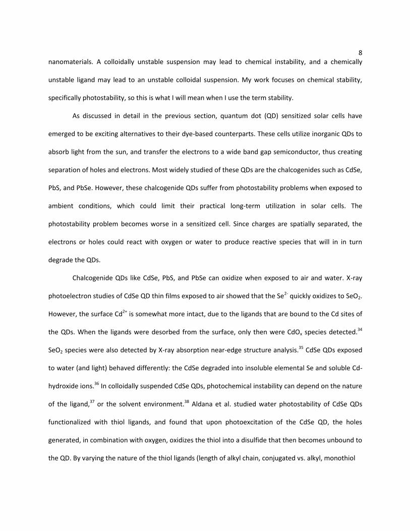
Figure 1.3: (a) CdSe QD coated with organic
dendron ligands, from ref. 39 (b) CdSe QD with
a ZnS shell, along with energy levels showing
the potential well created
ZnS
CdSe
CB
VB
(a)
(b)

10 vs. dithiol), they found that the most photostable CdSe QDs are the ones that are coated with long
hydrocarbon chains to prevent diffusion of oxygen into the QD core.37
There have been multiple methods developed to prevent the photo-oxidation of chalcogenide
QDs. Following the initial work of Aldana et al., as shown in Figure 1.3(a), ligands with large branched
hydrocarbons or dendrons were synthesized and found to stabilize QDs.39,40 Another route in using
organic ligand passivation is the encapsulation of the QD with polymers that contains multiple binding
groups on the polymer chain.41,42 QDs can also be protected from photodegradation with a wide-band
gap inorganic shell. The most common shell material for CdSe QDs is ZnS. As shown in Figure 1.3(b), the
energy levels of the ZnS shell are such that they trap the CdSe energy levels into a potential well, forcing
the photogenerated charges away from the surface. The inorganic shell also passivates the QD core
from surface and defect states.28 This passivation method is important for applications that require
stable, bright luminescence from the core, such as fluorescent tagging of biological materials.43
Insulating shell overcoats, such as ZnS,44 TiO2,45 and Al2O3
46,47 have also been used to protect QD-
sensitized systems either to passivate the absorbing QD from photodegradation or to reduce
recombination losses. In this case, since electrons need to transfer out of the QD into the electron
acceptor, the control of the shell thickness is important to not severely impede electron transfer.48,49
1.5 Surface Photovoltage Spectroscopy for Measurement of Charge Transfer and Charge Dynamics
As semiconductor technology becomes increasingly important in applications like computers
and optoelectronic devices, there is a continuing need to deepen our understanding of optical and
electronic properties of charge carriers in various semiconductor materials. Various spectroscopic
methods have been developed and utilized to characterize charge carriers in semiconductors; the most
common ones are pump-probe (either in transmission or reflection mode), photoluminescence,
photoemission, and surface photovoltage spectroscopies.50 Surface photovoltage (SPV) spectroscopy
has emerged to be very attractive and useful due to the advantages it has over the other techniques. It
11 is a non-contact, non-destructive technique does not require the sample to be either transmissive or
reflective (unlike pump-probe), have strong radiative emission bands (unlike photoluminescence), or be
performed under ultrahigh vacuum conditions (unlike photoemission).
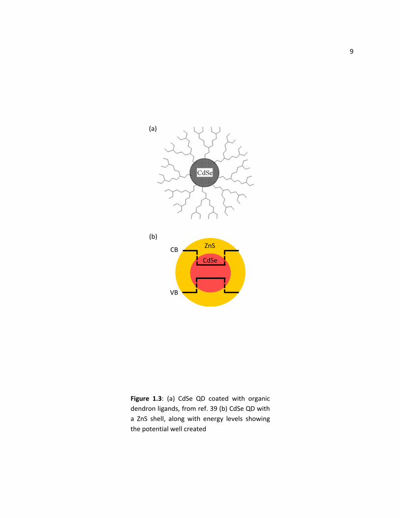
SPV measurements rely on the spatial separation of charge, either due to a semiconductor
space charge layer, or charge transfer from a dye/semiconductor heterojunction. The space charge
forms due to the fact that the termination of lattice periodicity at the surface of a semiconductor
introduces dangling bonds, surface atom rearrangements, or surface defects. This creates surface states
on the semiconductor that are usually located in the middle of the bandgap. At equilibrium, the charge
carriers redistribute between surface and bulk states, and subsequently the near-surface region of the
semiconductor develops an internal electric field. This deviation in electronic energies from the bulk is
represented and described by a band bending of the conduction and valence energy bands. Figure 1.4(a)
illustrates the band bending typical of an n-type semiconductor. As the semiconductor is photoexcited,
electrons generated feel this electric field, so charges separate spatially, changing the voltage at the
surface. SPV is the result of this photoinduced change in voltage. For an n-type semiconductor, electrons
will be driven deeper into the bulk, while the holes are left at the surface. In a dye/nanocrystal-
sensitized heterojunction system, spatial separation of charges is achieved by a charge transfer from the
sensitizer into an appropriate semiconductor acceptor. Specifically, for the dye-sensitized or the CdSe-
sensitized TiO2 systems discussed previously, electrons are transferred into the conduction band of TiO2,
while the holes are left on the sensitizing material (see Figure 1.1).
There are two main experimental configurations for the detection and measurement of SPV. The
first is the Kelvin probe method that relies on the direct relationship between surface work function and
surface photovoltage. I will not expand further on the Kelvin probe method (please see literature cited if
interested), as my SPV work focusses on the second approach, the metal-insulator-semiconductor (MIS)
setup. The MIS structure creates a capacitor-like arrangement, as shown in Figure 1.4(b). Upon
12
Figure 1.4: (a) Energy diagram showing band bending of a typical n-
type semiconductor (b) Schematic of the MIS capacitive setup for SPV
measurement. The setup illustrates the SPV signal resulting from the
spatial separation of charges in a sensitized system
-
+ hν
Ec
Ev
EF
(a)
hν
sense electrode
sample
+ + + +
- - - -
Insulating space
(b)
Sensitizer
13 illumination of the photoactive material, charges of one type accumulate on the surface due to the SPV
mechanisms discussed above. The ‘sense’ electrode, held close to the sample, builds up the charge of
the opposite sign and the corresponding voltage change can be externally measured. To achieve high
signal-to-noise, this is typically performed by illuminating with chopped light and measuring with a lock-
in amplifier.51
SPV spectroscopy has traditionally been used to characterize Si wafers and other simple single
crystal semiconductors (e.g. surface defect sites, effect of surface treatments), but more recently has
been extended to a few nanostructured semiconductors.52-54 The non-contact setup that is independent
of light reflection or scattering makes it very convenient for opaque or rough surfaces that are common
for nanostructured materials. This technique has also been used to characterize charge transfer across
dye and inorganic nanocrystal sensitized systems.55-58 Transient SPV techniques, on the other hand, are
less well-developed, and would be extremely beneficial for characterization of fast dynamics of charge
transfer (as in a sensitized solar cell), and exploration of earth-abundant semiconductors such as
hematite and iron pyrite that have short carrier lifetimes (< 1 ns) for solar photo-electrical/-
electrochemical applications.
1.6 Scope of Thesis
Chapters 2 and 3 are about the potential of using small organic conjugated ligands to enhance
the photostability of CdSe QD sensitized TiO2. Unlike long insulating hydrocarbons or insulating wide
bandgap shell, these ligands could provide an alternative pathway to passivation of air-sensitive
nanocrystals. Chapter 2 explores the influence of hole-trapping thiols on the photostability of CdSe
quantum dots (QDs). We show that by having conjugated ligands with electron-donating substituents,
we can stabilize the QD by a hole transfer, and subsequently the delocalization of the hole in the ligand.
Chapter 3 is further photostability studies of CdSe QDs, in which we explored the use of conjugated
bidentate ligands, specifically dithiocarbarmates (R-NCS2-). We were able to functionalize

14 dithiocarbamate (DTC) ligands on CdSe-TiO2 surfaces in-situ, and further found that the
dithiocarbarmates enhanced the photostability of CdSe QDs more than the monodentate thiols. This
enhancement is likely due to an increased electronic coupling to the QD. Chapter 4 is a brief work on the
possibility of using spectroelectrochemistry to elucidate the mechanism of triiodide reduction on Pt and
poly(3,4-ethylenedioxythiophene) poly(styrenesulfonate), an alternative DSSC counter electrode
material. Chapter 5 describes our efforts in the development of surface photovoltage (SPV) methods for
measurement of charge transfer and charge dynamics, in particular time-resolved methods, both in the
nanosecond and in the picosecond timescales. Finally, in chapter 6, I discuss my outlook and possible
future directions of my thesis work.
1.7 References
1. Green, M. A. Third Generation Photovoltaics: Solar Cells for 2020 and Beyond, Physica E 2002, 14, 65-70.
2. O'Regan, B.; Grätzel, M. A Low-Cost, High-Efficiency Solar-Cell Based on Dye-Sensitized Colloidial TiO2 Films, Nature 1991, 353, 737-740.
3. Memming, R. Semiconductor Electrochemistry; Wiley-VCH: Weinheim, Germany, 2001.
4. Grätzel, M. Dye-Sensitized Solar Cells, J. Photochem. Photobiol. C-Photochem. Rev. 2003, 4, 145-153.
5. Klahr, B. M.; Hamann, T. W. Performance Enhancement and Limitations of Cobalt Bipyridyl Redox Shuttles in Dye-Sensitized Solar Cells, J. Phys. Chem. C 2009, 113, 14040-14045.
6. Nusbaumer, H.; Moser, J. E.; Zakeeruddin, S. M.; Nazeeruddin, M. K.; Grätzel, M. Co-II(dbbiP)(2)(2+) Complex Rivals Tri-iodide/Iodide Redox Mediator in Dye-Sensitized Photovoltaic Cells, J. Phys. Chem. B 2001, 105, 10461-10464.
7. Nusbaumer, H.; Zakeeruddin, S. M.; Moser, J. E.; Grätzel, M. An Alternative Efficient Redox Couple for the Dye-Sensitized Solar Cell System, Chem.–Eur. J. 2003, 9, 3756-3763.
8. Sapp, S. A.; Elliott, C. M.; Contado, C.; Caramori, S.; Bignozzi, C. A. Substituted Polypyridine Complexes of Cobalt(II/III) as Efficient Electron-Transfer Mediators in Dye-Sensitized Solar Cells, J. Am. Chem. Soc. 2002, 124, 11215-11222.
9. Hamann, T. W.; Ondersma, J. W. Dye-Sensitized Solar Cell Redox Shuttles, Energy Environ. Sci. 2011, 4, 370-381.

15 10. Anderson, A. Y.; Barnes, P. R. F.; Durrant, J. R.; O'Regan, B. C. Simultaneous Transient Absorption
and Transient Electrical Measurements on Operating Dye-Sensitized Solar Cells: Elucidating the Intermediates in Iodide Oxidation, J. Phys. Chem. C 2010, 114, 1953-1958.
11. Boschloo, G.; Hagfeldt, A. Characteristics of the Iodide/Triiodide Redox Mediator in Dye-Sensitized Solar Cells, Acc. Chem. Res. 2009, 42, 1819-1826.
12. Clifford, J. N.; Palomares, E.; Nazeeruddin, M. K.; Grätzel, M.; Durrant, J. R. Dye Dependent Regeneration Dynamics in Dye Sensitized Nanocrystalline Solar Cells: Evidence for the Formation of a Ruthenium Bipyridyl Cation/Iodide Intermediate, J. Phys. Chem. C 2007, 111, 6561-6567.
13. Rowley, J.; Meyer, G. J. Reduction of I-2/I-3(-) by Titanium Dioxide, J. Phys. Chem. C 2009, 113, 18444-18447.
14. Ahmad, S.; Yum, J.-H.; Zhang, X.; Grätzel, M.; Butt, H.-J.; Nazeeruddin, M. K. Dye-Sensitized Solar Cells Based on Poly (3,4-ethylenedioxythiophene) Counter Electrode Derived from Ionic Liquids, J. Mater. Chem. 2010, 20, 1654-1658.
15. Kanciurzewska, A.; Dobruchowska, E.; Baranzahi, A.; Carlegrim, E.; Fahlman, M.; Girtu, M. A. Study on Poly(3,4-ethylene dioxythiophene)-Poly(styrenesulfonate) as a Plastic Counter Electrode in Dye Sensitized Solar Cells, J. Optoelectron. Adv. Mater. 2007, 9, 1052-1059.
16. Li, Q.; Wu, J.; Tang, Q.; Lan, Z.; Li, P.; Lin, J.; Fan, L. Application of Microporous Polyaniline Counter Electrode for Dye-Sensitized Solar Cells, Electrochem. Commun. 2008, 10, 1299-1302.
17. Murakami, T. N.; Graetzel, M. Counter Electrodes for DSC: Application of Functional Materials as Catalysts, Inorg. Chim. Acta 2008, 361, 572-580.
18. Trancik, J. E.; Barton, S. C.; Hone, J. Transparent and Catalytic Carbon Nanotube Films, Nano Lett. 2008, 8, 982-987.
19. Hou, Y.; Wang, D.; Yang, X. H.; Fang, W. Q.; Zhang, B.; Wang, H. F.; Lu, G. Z.; Hu, P.; Zhao, H. J.; Yang, H. G. Rational Screening Low-Cost Counter Electrodes for Dye-Sensitized Solar Cells, Nat. Commun. 2013, 4, 1583-1583.
20. Wu, M.; Lin, X.; Hagfeldt, A.; Ma, T. A Novel Catalyst of WO2 Nanorod for the Counter Electrode of Dye-Sensitized Solar Cells, Chem. Comm. 2011, 47, 4535-4537.
21. Wu, M.; Lin, X.; Wang, Y.; Wang, L.; Guo, W.; Qu, D.; Peng, X.; Hagfeldt, A.; Graetzel, M.; Ma, T. Economical Pt-Free Catalysts for Counter Electrodes of Dye-Sensitized Solar Cells, J. Am. Chem. Soc. 2012, 134, 3419-3428.
22. Wang, M.; Anghel, A. M.; Marsan, B.; Ha, N.-L. C.; Pootrakulchote, N.; Zakeeruddin, S. M.; Graetzel, M. CoS Supersedes Pt as Efficient Electrocatalyst for Triiodide Reduction in Dye-Sensitized Solar Cells, J. Am. Chem. Soc. 2009, 131, 15976-15977.
16 23. Sun, H.; Qin, D.; Huang, S.; Guo, X.; Li, D.; Luo, Y.; Meng, Q. Dye-Sensitized Solar Cells with NiS
Counter Electrodes Electrodeposited by a Potential Reversal Technique, Energy Environ. Sci. 2011, 4, 2630-2637.
24. Li, G.-R.; Wang, F.; Jiang, Q.-W.; Gao, X.-P.; Shen, P.-W. Carbon Nanotubes with Titanium Nitride as a Low-Cost Counter-Electrode Material for Dye-Sensitized Solar Cells, Angew. Chem. Int. Ed. 2010, 49, 3653-3656.
25. Wu, M.; Lin, X.; Hagfeldt, A.; Ma, T. Low-Cost Molybdenum Carbide and Tungsten Carbide Counter Electrodes for Dye-Sensitized Solar Cells, Angew. Chem. Int. Ed. 2011, 50, 3520-3524.
26. Peter, L. M. The Grätzel Cell: Where Next?, J. Phys. Chem. Lett. 2011, 2, 1861-1867.
27. Kamat, P. V. Quantum Dot Solar Cells. The Next Big Thing in Photovoltaics, J. Phys. Chem. Lett. 2013, 4, 908-918.
28. Smith, A. M.; Nie, S. Semiconductor Nanocrystals: Structure, Properties, and Band Gap Engineering, Acc. Chem. Res. 2010, 43, 190-200.
29. Tvrdy, K.; Frantsuzov, P. A.; Kamat, P. V. Photoinduced Electron Transfer from Semiconductor Quantum Dots to Metal Oxide Nanoparticles, Proc. Natl. Acad. Sci. U.S.A. 2011, 108, 29-34.
30. Albe, V.; Jouanin, C.; Bertho, D. Confinement and Shape Effects on the Optical Spectra of Small CdSe Nanocrystals, Phys. Rev. B 1998, 58, 4713-4720.
31. Acharya, K. P.; Alabi, T. R.; Schmall, N.; Hewa-Kasakarage, N. N.; Kirsanova, M.; Nemchinov, A.; Khon, E.; Zamkov, M. Linker-Free Modification of TiO2 Nanorods with PbSe Nanocrystals, J. Phys. Chem. C 2009, 113, 19531-19535.
32. Kang, I.; Wise, F. W. Electronic Structure and Optical Properties of PbS and PbSe Quantum Dots, J. Opt. Soc. Am. B: Opt. Phys. 1997, 14, 1632-1646.
33. Nozik, A. J. Nanoscience and Nanostructures for Photovoltaics and Solar Fuels, Nano Lett. 2010, 10, 2735-2741.
34. Katari, J. E. B.; Colvin, V. L.; Alivisatos, A. P. X-ray Photoelectron Spectroscopy of CdSe Nanocrystals with Applications to Studies of the Nanocrystal Surface, J. Phys. Chem. 1994, 98, 4109-4117.
35. Hines, D. A.; Becker, M. A.; Kamat, P. V. Photoinduced Surface Oxidation and Its Effect on the Exciton Dynamics of CdSe Quantum Dots, J. Phys. Chem. C 2012, 116, 13452-13457.
36. Xi, L.; Lek, J. Y.; Liang, Y. N.; Boothroyd, C.; Zhou, W.; Yan, Q.; Hu, X.; Chiang, F. B. Y.; Lam, Y. M. Stability studies of CdSe Nanocrystals in an Aqueous Environment, Nanotechnology 2011, 22.
37. Aldana, J.; Wang, Y. A.; Peng, X. G. Photochemical Instability of CdSe Nanocrystals Coated by Hydrophilic Thiols, J. Am. Chem. Soc. 2001, 123, 8844-8850.
17 38. Manner, V. W.; Koposov, A. Y.; Szymanski, P.; Klimov, V. I.; Sykora, M. Role of Solvent-Oxygen
Ion Pairs in Photooxidation of CdSe Nanocrystal Quantum Dots, ACS Nano 2012, 6, 2371-2377.
39. Wang, Y. A.; Li, J. J.; Chen, H. Y.; Peng, X. G. Stabilization of Inorganic Nanocrystals by Organic Dendrons, J. Am. Chem. Soc. 2002, 124, 2293-2298.
40. Guo, W. H.; Li, J. J.; Wang, Y. A.; Peng, X. G. Luminescent CdSe/CdS Core/Shell Nanocrystals in Dendron Boxes: Superior Chemical, Photochemical and Thermal Stability, J. Am. Chem. Soc. 2003, 125, 3901-3909.
41. Potapova, I.; Mruk, R.; Prehl, S.; Zentel, R.; Basche, T.; Mews, A. Semiconductor Nanocrystals with Multifunctional Polymer Ligands, J. Am. Chem. Soc. 2003, 125, 320-321.
42. Yildiz, I.; McCaughan, B.; Cruickshank, S. F.; Callan, J. F.; Raymo, F. M. Biocompatible CdSe-ZnS Core-Shell Quantum Dots Coated with Hydrophilic Polythiols, Langmuir 2009, 25, 7090-7096.
43. Medintz, I. L.; Uyeda, H. T.; Goldman, E. R.; Mattoussi, H. Quantum Dot Bioconjugates for Imaging, Labelling and Sensing, Nat. Mater. 2005, 4, 435-446.
44. Barea, E. M.; Shalom, M.; Gimenez, S.; Hod, I.; Mora-Sero, I.; Zaban, A.; Bisquert, J. Design of Injection and Recombination in Quantum Dot Sensitized Solar Cells, J. Am. Chem. Soc. 2010, 132, 6834-6839.
45. Shalom, M.; Dor, S.; Ruhle, S.; Grinis, L.; Zaban, A. Core/CdS Quantum Dot/Shell Mesoporous Solar Cells with Improved Stability and Efficiency Using an Amorphous TiO(2) Coating, J. Phys. Chem. C 2009, 113, 3895-3898.
46. Ihly, R.; Tolentino, J.; Liu, Y.; Gibbs, M.; Law, M. The Photothermal Stability of PbS Quantum Dot Solids, ACS Nano 2011, 5, 8175-8186.
47. Choi, H.; Nicolaescu, R.; Paek, S.; Ko, J.; Kamat, P. V. Supersensitization of CdS Quantum Dots with a Near-Infrared Organic Dye: Toward the Design of Panchromatic Hybrid-Sensitized Solar Cells, ACS Nano 2011, 5, 9238-9245.
48. Brennan, T. P.; Bakke, J. R.; Ding, I. K.; Hardin, B. E.; Nguyen, W. H.; Mondal, R.; Bailie, C. D.; Margulis, G. Y.; Hoke, E. T.; Sellinger, A.; et. al. The Importance of Dye Chemistry and TiCl4 Surface Treatment in the Behavior of Al2O3 Recombination Barrier Layers Deposited by Atomic Layer Deposition in Solid-State Dye-Sensitized Solar Cells, Phys. Chem. Chem. Phys. 2012, 14, 12130-12140.
49. Guo, J.; She, C.; Lian, T. Effect of Insulating Oxide Overlayers on Electron Injection Dynamics in Dye-Sensitized Nanocrystalline Thin Films, J. Phys. Chem. C 2007, 111, 8979-8987.
50. Khanna, V. K. Physical Understanding and Technological Control of Carrier Lifetimes in Semiconductor Materials and Devices: A Critique of Conceptual Development, State of the Art and Applications, Prog. Quant. Electron. 2005, 29, 59-163.

18 51. Kronik, L.; Shapira, Y. Surface photovoltage phenomena: Theory, Experiment, and Applications,
Surf. Sci. Rep. 1999, 37, 1-206.
52. Caban-Acevedo, M.; Faber, M. S.; Tan, Y.; Hamers, R. J.; Jin, S. Synthesis and Properties of Semiconducting Iron Pyrite (FeS2) Nanowires, Nano Lett. 2012, 12, 1977-1982.
53. Duzhko, V.; Timoshenko, V. Y.; Koch, F.; Dittrich, T. Photovoltage in Nanocrystalline Porous TiO2, Phys. Rev. B 2001, 64.
54. Li, L.; Yu, Y.; Meng, F.; Tan, Y.; Hamers, R. J.; Jin, S. Facile Solution Synthesis of α-FeF3·3H2O Nanowires and Their Conversion to α-Fe2O3 Nanowires for Photoelectrochemical Application, Nano Lett. 2012, 12, 724-731.
55. Jiang, T.; Xie, T.; Zhang, Y.; Chen, L.; Peng, L.; Li, H.; Wang, D. Photoinduced Charge Transfer in ZnO/Cu2O Heterostructure Films Studied by Surface Photovoltage Technique, Phys. Chem. Chem. Phys. 2010, 12, 15476-15481.
56. Mora-Sero, I.; Bisquert, J.; Dittrich, T.; Belaidi, A.; Susha, A. S.; Rogach, A. L. Photosensitization of TiO2 Layers with CdSe Quantum Dots: Correlation between Light Absorption and Photoinjection, J. Phys. Chem. C 2007, 111, 14889-14892.
57. Mora-Sero, I.; Dittrich, T.; Susha, A. S.; Rogach, A. L.; Bisquert, J. Large Improvement of Electron Extraction from CdSe Quantum Dots into a TiO2 Thin Layer by N3 Dye Coabsorption, Thin Solid Films 2008, 516, 6994-6998.
58. Zillner, E.; Dittrich, T. Surface Photovoltage within a Monolayer of CdSe Quantum Dots, Phys. Status Solidi RRL 2011, 5, 256-258.
19
Chapter 2
Influence of Hole-Sequestering Ligands on the Photostability of CdSe Quantum
Dots
A part of this work is published in J. Phys. Chem. C, 117, 313 – 320
2.1 Introduction
Inorganic semiconductor quantum dots (QDs) are promising alternatives to organic dyes as
visible-light absorbers in sensitized solar cells.1-3 Inorganic QDs are advantageous because their optical
and electronic properties are size dependent and therefore can be tuned to optimize solar absorption as
well as the energy alignment between QD and metal oxide acceptor for favourable electron transfer.4-6
In addition, recent studies have demonstrated that some QDs have the ability to support hot electrons7,8
or multiple excitons per incident photon.9-12 Various semiconductor QDs such as CdSe,4,13 PbSe,5,6,8,14 and
PbS11,15,16 have been studied as sensitizers for quantum dot sensitized solar cells.
While QDs have many outstanding properties, the practical utilization of chalcogenide QDs is
hindered by their propensity to undergo oxidation,17-21 requiring strictly air- and water-free conditions to
remain stable. Protective inorganic shells such as ZnS13 and Al2O322 have been used to passivate the
surface and control their photooxidation, but these wide-bandgap shells may introduce potential
barriers to charge transfer if their thickness is not properly controlled.23,24
Compounds containing aromatic amino groups are widely used as hole conductors, but in
general these are larger molecules or polymers with more extensive conjugation.25,26 These groups are
also widely used in donor-π-acceptor type structures for dye-sensitized solar cells, with the arylamine
acting as an electron donor.27-29 A similar approach can be used to remove oxidizing holes from a QD, by
functionalizing the QD with hole-accepting ligands. This chapter is about our work on the influence of
20
Oleic Acid (OA)
1-Dodecanethiol (DT)
4-Dimethylaminothiophenol (DMATP)
Thiophenol(TP)
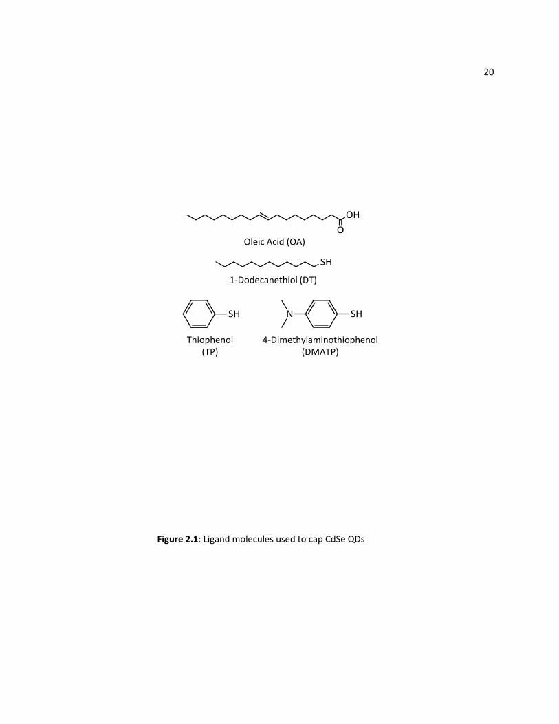
Figure 2.1: Ligand molecules used to cap CdSe QDs
21 hole-accepting ligands on the stability of CdSe QDs and on CdSe-sensitized TiO2 (referred to as
CdSe/TiO2). Figure 2.1 shows the ligands investigated here. Our results show that small conjugated
ligands slow photocorrosion in comparison with long alkyl ligands. In particular, an electron donating
amino group in the conjugated ligand, such as in 4-dimethylaminothiophenol (DMATP, see Figure 2.1),
provides remarkable stabilization of CdSe QDs. We combine photocorrosion, photoluminescence, and
density functional calculations to understand how molecular structure of the ligand affects QD stability.
Our results show that removing localized charge from the sulfur with an electron-donating amino group
stabilizes the ligand and minimizes photocorrosion of the QD. Finally, we discuss our attempts in utilizing
DMATP-passivated CdSe in a liquid junction QD sensitized solar cell, and our efforts in extending this
DMATP ligand passivation idea to PbS and PbSe QDs.
2.2 Experimental
2.2.1 Chemicals
Trioctylphosphine oxide (TOPO) 99+%, CdO 99.99% metal basis, Oleic Acid (OA) 90%,
Trioctylphosphine (TOP) 90%, Selenium 99.99% metal basis, 3-Mercaptopropionic Acid (MPA) 99+%, 1-
Dodecanethiol (DT) 98+%, Thiophenol (TP) ≥99% were purchased from Sigma-Aldrich. 4-
Dimethylaminothiophenol (DMATP) was purchased from Oakwood Products.
2.2.2 Preparation of Nanocrystalline TiO2 Films
Fluorine-doped tin oxide (FTO) coated glass (Hartford Glass) was pre-cleaned with detergent,
acetone and ethanol. Anatase TiO2 nanoparticles (average diameter = 20 nm) in a form of a paste (Ti-
Nanoxide, T20/SP, Solartonix) was screen-printed onto the FTO glass to give ~ 2 μm thick films. The
screen-printing process produces multiple films with the same thickness and mesoporous structure.
Each experimental set described here was performed using films prepared from the same batch of films.
These films of 0.5 cm in diameter were then sintered and annealed in air following a procedure adapted
from literature30 at 325 C for 5 min, at 375 C for 5 min, and at 450 C for 15 min, and finally, at 500 C

22
for 30 min. Before use, the films were given an additional annealing step at 500 C for 15 min to remove
any adsorbed water and organic contaminants.
2.2.3 Synthesis of CdSe QDs
The synthesis was adapted from Peng and Peng.31 Briefly, 3.1 g TOPO, 0.23 g CdO, and 1.8 g OA
are combined into a 3-necked flask. The mixture was then heated under Ar flow until it turned optically
clear (~290 C). The mixture was then allowed to cool to 250 C. A solution of TOPSe made by combining
0.04 g Se and 1.2 mL TOP was injected to the flask. The reaction was cooled to ~80 C, and was then
quenched with toluene. The CdSe QD solution was purified four times by precipitation and
centrifugation with methanol. The size and concentration of the CdSe QDs were determined from the
wavelength and absorbance of the first exciton peak, using empirical relationships established by Peng
and co-workers.32 This analysis yielded particle diameters that were typically 3.0 - 3.2 nm. The QDs were
kept in toluene and in the dark until further use. These as-synthesized QDs will be referred to as OA-
CdSe.
2.2.4 CdSe-TiO2 Adduct Formation and Subsequent Ligand Exchange
After synthesis, the CdSe nanoparticles were linked to TiO2 by one of two methods: (1) using a
bifunctional ligand to provide a covalent CdSe-TiO2 linkage, or (2) by direct physical adsorption. Ligand
exchange was performed after the CdSe nanoparticles were attached to TiO2 to investigate the effect of
the ligands on physical properties of the CdSe nanoparticles. Attachment of CdSe to TiO2 via covalent
linkage was performed using 3-mercaptopropionic acid (MPA). This approach provides obtain good
control over CdSe coverage.33-35 The TiO2 films were immersed in 0.1 M MPA in anhydrous acetonitrile
(ACN) for 6 – 8 h in the dark. They were rinsed with anhydrous ACN and toluene. Samples were then
immersed in 20 – 50 μM CdSe QDs in toluene (QD molarities in this work are defined by number of
moles of QDs per liter of solution) for 16 – 18 h in the dark, and rinsed with toluene. Functionalization
with ligands depicted in Figure 2.1 was then performed by soaking the samples in a solution of the

23 respective ligand (0.1 M in toluene, or just pure toluene for the OA sample) for ~24 h in the dark. They
were rinsed with toluene, then heptane, and dried with N2. Experiments were also conducted using
direct absorption of CdSe QDs to TiO2 with no linker; in this case the CdSe QDs (also 20 – 50 μM) were
precipitated with methanol, centrifuged, and resuspended in dichloromethane (DCM). The TiO2 films
were then immersed in the QD/DCM solution for 24 h,35 rinsed with DCM, and dried with N2.
2.2.5 Fourier Transform Infrared (FTIR) Spectroscopy
All measurements were taken with a Vertex 70 (Bruker) spectrometer at a resolution of 4 cm-1
and constant dry-air purging. The L-CdSe/TiO2 surfaces were measured in single-bounce reflection
absorption mode (VeeMax II accessory, Pike Technologies) with p-polarized light at an incident angle of
50 from the sample normal. The spectra were referenced against a clean TiO2 film prepared using
identical procedures. To minimize effects of atmospheric water and CO2 each sample and the clean TiO2
reference sample were measured as closely together in time as possible. This method of referencing
produced the most reproducible results.
2.2.6 X-ray Photoelectron Spectroscopy (XPS)
Measurements were done on a custom-built XPS system (Physical Electronics) with an Al-Kα
source (Model 10-610, 1486.6 eV photon energy), torroidal monochromator (Model 10-420), and
hemispherical analyzer with a 16 channel detector array (Model 10-360). We used an electron takeoff
angle of 45 and measured at a resolution of 0.05 or 0.1 eV. Peak areas were obtained by fitting the
spectra to a Voigt function. Shirley baseline corrections were used as needed.
2.2.7 Photodegradation Studies
For studies in H2O, the samples were sandwiched into a cell with another piece of FTO glass and
a 127 μm spacer; the open region was filled with 18 MΩ·cm H2O (Barnstead Nanopure). The cell has
windows to allow light penetration and time-dependent absorption studies without disassembling the
cell. The sample was illuminated through the plain FTO piece and water onto the sample. Light from a
24 solar simulator (Newport 91160, equipped with AM1.5G filters and set to 100 mW/cm2 as measured by
a Scientech calorimeter) was passed through a filter transmitting only light with wavelengths longer
than 475 nm. This filter was used to ensure that light is only absorbed by the CdSe QD, and not by the
TiO2. With the filter, the irradiance was measured to be 81 mW/cm2. This optical setup was used for all
of our degradation studies. Transmission UV-visible absorbance spectra (Shimadzu, UV-2401PC) were
obtained up to 10 min of exposure time. For studies in air, samples were left under the light under
ambient conditions without assembly into a cell. Absorption spectra were taken at exposure times up to
15 min.
2.2.8 Photoluminescence (PL)
The QDs were precipitated with methanol, centrifuged and resuspended with chloroform to give
~2 μM concentration. In all of the experiments, they were excited with 450 nm light, close to the second
absorption peak that corresponds to the second excitonic transition. Ligands, at a concentration of ~70
μM, were added and mixed immediately before experiments. Steady state experiments were performed
using an ISS K2 fluorometer. For transient PL measurements, 3 ns pulses from a laser (Ekspla NT340,
Nd:YAG with an optical parametric oscillator 250 μJ/pulse, 20 pulses/sec) were used to excite the QDs.
The transient fluorescence was collected with a photomultiplier tube (Hamamatsu R6357, rise time 1.4
ns) and recorded using an oscilloscope (Agilent, DSO5054A, 500MHz).
2.2.9 Density Functional Theory (DFT) Calculations
In order to better understand the nature of charge separation in these compounds, we
performed DFT calculations of the relevant molecules, using a Cd6Se6 cluster to model the CdSe surface.
Calculations were performed using the Gaussian09 program using the B3LYP hybrid density functional
and the LANL2DZ basis set for all atoms.36 Calculations on the free molecules were also performed using
the Dunning-Hay D95 basis set;37 since these results were nearly identical to those using the LANL2DZ
basis set all results reported here used the latter. The CdSe cluster was constrained to maintain the
25 property symmetry while leaving all bond distances unconstrained. A Natural Bond Orbital (NBO)
analysis38 was used to determine the charges on the individual atoms.
2.2.10 Fabrication of CdSe Sensitized TiO2 Solar Cells
TiO2 electrodes on FTO glass were made following a procedure adapted from literature.30 The
TiO2 films were first subjected to a TiCl4 pre-treatment to obtain a dense 1 nm thick TiO2 film. Three
screen-print passes were done with a drying step at 125 C for 5 min in between passes to yield 3 μm
thick films. We did not deposit a scattering layer because we found that the presence of the diffuse film
blocked the absorption of QDs into the pores of the TiO2 film. The films were subsequently annealed
using the procedure described above. After annealing, the films were subjected to another TiCl4
treatment step. The films were cleaned by heating at 500 C for 15 min prior to use. CdSe QDs were
functionalized to the TiO2 by direct physical absorption (no linker used) as described above. The redox
electrolyte was 0.22 M Co(bpy)3(PF6)2, 0.033 M Co(bpy)3(PF6)3, 0.2 M tert-butylpyridine, and 0.1 M
LiClO4.39 The counter electrode was a platinized FTO glass, made by coating the FTO piece with a drop of
0.1 M H2PtCl6 solution in ethanol and heating the piece at 450 C for 15 min.30
2.3 Results
2.3.1 FTIR Characterization of Functionalized CdSe/TiO2 Surfaces
Figure 2.2(a) shows FTIR spectra of CdSe/TiO2 functionalized with different ligands used in this
work (labeled as L-CdSe/TiO2 where L = OA, DT, TP, or DMATP). Spectra of the neat ligands are shown in
Figure 2.2(b). The CdSe QDs, as functionalized on TiO2 exhibit C-H peaks at 2856 and 2928 cm-1, close to
the 2854 and 2924 cm-1 of neat OA and a C-H peak at 3005 cm-1 from the C=CH group of oleic acid. These
nanoparticles show two peaks at 1551 and 1404 cm-1 that are characteristic of the carboxylate group,
while neat OA shows a single large peak at 1710 cm-1 in agreement with previous studies.40,41 The peaks
at 1551 and 1404 have previously been attributed to the asymmetric and symmetric stretching vibration
modes (respectively) of carboxylate groups bonded to CdS surfaces while 1710 cm-1 is typical

26
0.05
Inte
nsi
ty
OA
DT
TP
DMATP
Wavenumbers (cm-1)
-C-H=C-H
3000 2600 1600 1200
(Ar)C-H
carboxylate
(Ar)C-H
1800 1600 1400 1200 10003200 3000 2800 2600
0.05Oleic Acid
1-Dodecanethiol
Thiophenol
4-Dimethylaminothiophenol
Inte
nsi
ty
Wavenumbers (cm-1)
(a)
(b)
Figure 2.2: (a) IR spectra of L-CdSe/TiO2 indicating binding of ligands to the
surface. The 3160-2980 cm-1 region is enlarged 8x and overlaid directly
above each spectra. Ar = Aromatic (b) IR spectra of neat ligands
27 of the C=O stretch of a free carboxylic acid.40 Both OA on CdSe and MPA bound to TiO2 contribute to
these carboxylate peaks. Therefore, they are still present even after the displacement of OA molecules
with other ligands. The DT functionalized sample, shows similar features but is marked by the absence
of any significant intensity near 3005 cm-1, thereby indicating removal of the oleic acid groups. The TP-
modified samples show a C-H feature at 3061 cm-1, slightly lower that the ~3070 cm-1 observed for the
parent compound, while and DMATP-CdSe/TiO2 samples show a peak at 3076 cm-1. These features are
nearly identical to those observed previously for thiophenol on gold and attributed to the aromatic C-H
stretching modes.42 The DMATP samples show a more complex spectrum in the 2700-3000 cm-1 region
where the C-H modes of the -N(CH3)2 groups would be expected; this region is similar to that of the pure
parent compound and of N,N-dimethylaniline.43 Our FTIR data establish that ligand exchange from the
initially functionalized samples is successful, although some small amounts of OA may remain. The
asymmetric CH2 stretch of OA-CdSe/TiO2 and DT-CdSe/TiO2 occur at 2927 and 2926 cm-1 respectively,
slightly larger than the value of 2924 cm-1 for neat OA and DT. In contrast, prior studies have found that
the asymmetric mode decreases by ~ 6 – 8 cm-1 when forming a crystalline monolayer.44 Thus, our FTIR
data indicate that the OA and DT layers formed on CdSe are in a very fluidic local environment.
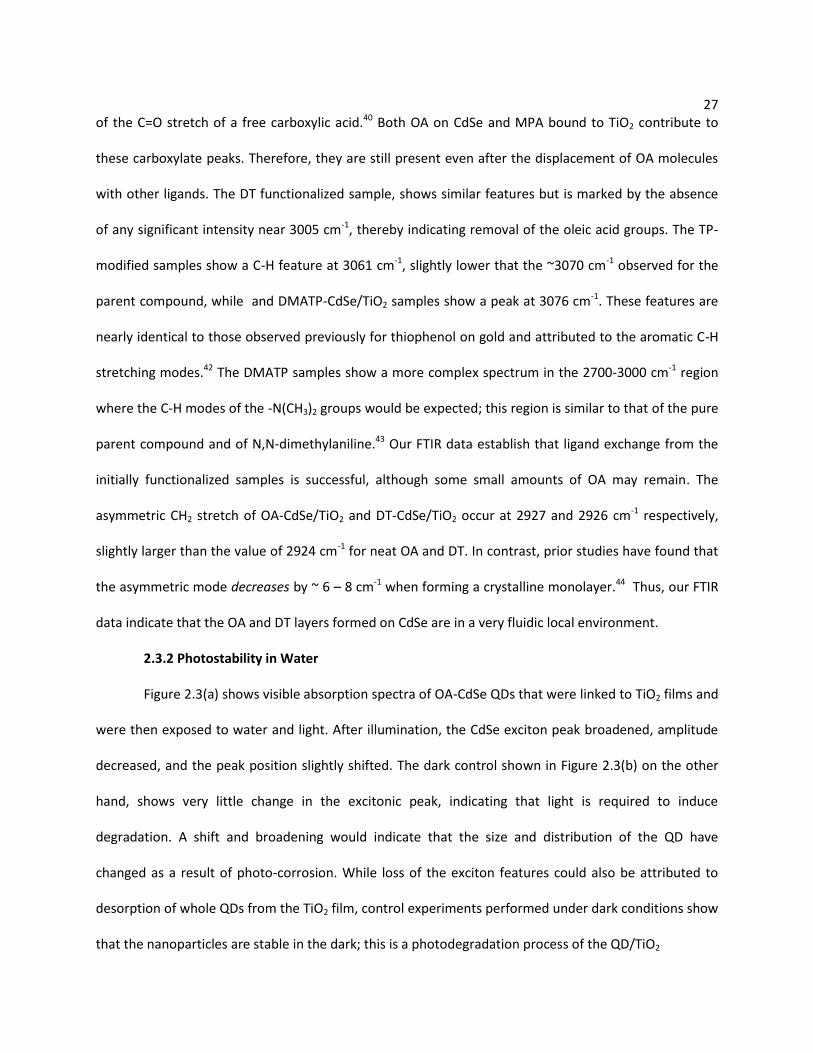
2.3.2 Photostability in Water
Figure 2.3(a) shows visible absorption spectra of OA-CdSe QDs that were linked to TiO2 films and
were then exposed to water and light. After illumination, the CdSe exciton peak broadened, amplitude
decreased, and the peak position slightly shifted. The dark control shown in Figure 2.3(b) on the other
hand, shows very little change in the excitonic peak, indicating that light is required to induce
degradation. A shift and broadening would indicate that the size and distribution of the QD have
changed as a result of photo-corrosion. While loss of the exciton features could also be attributed to
desorption of whole QDs from the TiO2 film, control experiments performed under dark conditions show
that the nanoparticles are stable in the dark; this is a photodegradation process of the QD/TiO2
28
0.4
0.6
0.8
1
A/A
0
1050exposure time (min)
OAOA,
dark controlDTTPDMATP
0.3
0.2
0.1
0.0
600500
peak only
raw data(OA, 0 min)
baseline
Wavelength (nm)
0.05
Ab
s
Wavelength (nm)
(a)
(c)
(e)
(d)
Ab
s
0 min 3
5 10
600550500
0 min310
600550500
OA,
dark control
OA
600560520
OAA
bs A0
A
0.02
(b)
Figure 2.3: (a) Visible absorption of OA-CdSe/TiO2 exposed to light and H2O at 0, 3, 10
min (b) the dark control for L = OA. Spectra stacked for clarity (c) Baseline subtraction
procedure used to obtain the peak. (d) Resulting peaks after baseline subtraction for L=
OA. (e) Fraction of original peak amplitude, A/A0 versus exposure time for all ligands.
Error bars are standard deviations obtained from four separate samples for each ligand
29 structure. After light exposure, significant changes were observed in the first exciton peak, but this peak
was riding on a large rising background. For subsequent analyses, we isolated the exciton peak by
subtracting the rising background as depicted in Figure 2.3(c) to quantify this degradation. The
background was fitted to a line in the region around the peak. Figure 2.3(d) shows the results of the
baseline subtraction. To systematically track the degradation, we calculated the fraction of original peak
amplitude, A/A0. A0 is the amplitude at the peak of the baselined curve at time = 0 min, while A is the
amplitude of time > 0 min, obtained at same wavelength as A0. This ratio was calculated for each sample
first, then averaged over multiple samples (prepared identically) for each ligand to evaluate the
statistical variation between samples.
We compared the photodegradation of CdSe/TiO2 adducts before and after substitution of the
native CdSe ligands with three different ligands (L) depicted in Figure 2.1: 4-dimethylaminothiophenol
(DMATP), thiophenol (TP), and 1-dodecanethiol (DT). Figure 2.3(e) shows the calculated ratio A/A0
plotted versus exposure time of the L-CdSe/TiO2 adducts after illumination in water. These data show
that thiol-substituted ligands on CdSe are more stable than those of the starting OA-CdSe/TiO2 adducts.
A comparison of all four ligands reveals that the order of stability is DMATP > TP ≈ DT > OA.
When comparing the thiol ligands used here, somewhat surprisingly, our results show that the
shorter, phenyl-terminated ligands provide comparable (in the case of TP) or better (in the case of
DMATP) stability than the long-chain dodecanethiol. In contrast, Aldana et al. reported that for thiols
terminated with carboxylic acids, the aromatic thiol-coated CdSe QDs were less stable than aliphatic
thiol-coated ones.45 Conjugation in the molecule can provide protection against degradation, with
DMATP outperforming the rest, as measured by the noticeably smaller change in the A/A0 values.
Notably, the dimethylamino group at the distal end of the DMATP molecule provides better protection
than the similar molecule lacking this group (i.e. thiophenol).
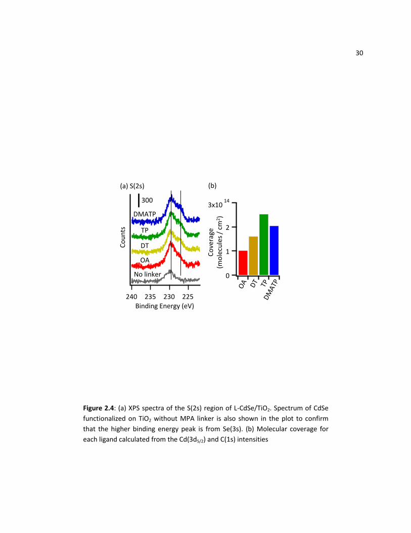
30
(a) S(2s) (b)
300
Co
un
ts
Binding Energy (eV)
No linker
240 235 230 225
DMATP
TP
DT
OA
3x10¹⁴
2
1
0
Co
vera
ge(m
ole
cule
s /
cm2)
Figure 2.4: (a) XPS spectra of the S(2s) region of L-CdSe/TiO2. Spectrum of CdSe
functionalized on TiO2 without MPA linker is also shown in the plot to confirm
that the higher binding energy peak is from Se(3s). (b) Molecular coverage for
each ligand calculated from the Cd(3d5/2) and C(1s) intensities

31 2.3.3 Comparison of Molecular Coverages
To investigate whether there were significant differences in packing of ligand molecules on the
CdSe QDs, XPS measurements were performed on freshly prepared samples to obtain their relative
coverages on CdSe QDs. Quantitative analysis of the S and Se regions is complicated by the fact that the
S(2s) and S(2p) peaks have significant overlap with the Se(3s) and Se(3p) peaks. Figure 2.4 shows the
sulfur 2s region; here, the peak at 230 eV was assigned to Se(3s), while the peak at 227 eV is assigned to
S(2s). This assignment was verified by fact that only the peak at 230 eV was observed when CdSe was
functionalized directly on TiO2 without using MPA linker. Quantitative analysis of molecular packing
densities on nanoparticulate samples must take into account the geometric shape of the nanoparticles
and inelastic scattering taking place within the nanoparticle core and the surface ligands.20 To properly
account for electron scattering effects, we used direct numerical integration to determine the ratio of C
to Cd signal expected from QDs of 1.6 nm radius surrounded by an organic layer, including full scattering
corrections. Details of the numerical integration and the parameters used are described in the Appendix
A1 section of this thesis. Figure 2.4(b) shows the resulting molecular packing densities determined from
the XPS data. The data show that DT, TP, DMATP molecules have similar packing densities; that of OA is
somewhat smaller, likely due to the labile nature of the carboxylic acid ligands, and the unsaturated
nature of the ligand, which disrupts packing crystallinity.46 These data show that the enhanced
photostability of DMATP cannot be explained simply on the basis of molecular packing densities.
2.3.4 Photostability in Air
The enhanced stability of DMATP-functionalized CdSe/TiO2 films is also evident in air. Figure 2.5
shows A/A0 values of L-CdSe/TiO2 plotted versus exposure time. The degradation in air is slightly slower
than that in water; while the OA sample had ~60% of the original peak amplitude after 10 min exposure
in air, the same OA ligand had only ~40% of the original amplitude after the same amount of exposure
time in water. In this case, desorption of whole QDs should not occur, as samples were not immersed in
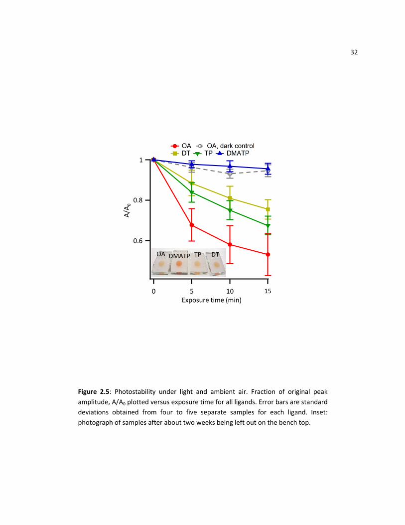
32
0.6
0.8
1
A/A
0
151050Exposure time (min)
OA DMATP TP DT
Figure 2.5: Photostability under light and ambient air. Fraction of original peak
amplitude, A/A0 plotted versus exposure time for all ligands. Error bars are standard
deviations obtained from four to five separate samples for each ligand. Inset:
photograph of samples after about two weeks being left out on the bench top.

33 liquid, therefore the photodegradation measured was from corrosion of the QD itself. The photo
degradation effects can also be seen visually in a photograph of the CdSe/TiO2 films that have been
functionalized with the ligands in this work exposed to ambient lighting for about two weeks (Figure 2.5
inset). After several days, only the DMATP-capped CdSe/TiO2 has retained its dark orange colour, the
films capped with other ligands became lighter in colour, turning from orange-red to pale-orange. The
enhanced stability of QDs that are capped with DMATP compared to other ligands is readily visible.
2.3.5 Photoluminescence
To understand the origins of this stability trend, we performed photoluminescence (PL)
experiments on the CdSe QDs in solution functionalized with the different capping ligands. Figure 2.6(a)
shows the steady-state emission of the CdSe QDs, while Figure 2.6(b) shows the transient luminescence.
Figure 2.6(a) shows that the thiol-capped CdSe QDs has much smaller fluorescence (~100-fold reduction
in intensity) compared with the OA-terminated QDs (note also the scale change, as the signal from the
OA-capped QDs has been reduced 10-fold). Thiol-capped CdSe QDs quenches the PL, as seen and
investigated by many others,47-51 and is thought to be due to hole transfer to the thiol end group.48,52
Trapping of holes in the ligand is a non-radiative pathway, therefore as the propensity of hole transfer
increases, PL quenching increases. The extent of quenching by capping ligand also agrees the
photostability trend; ligands that trap holes more efficiently lead to increased CdSe stability. When the
holes are pulled away from the CdSe into the ligand, oxidation to the CdSe itself is prevented. With the
DMATP ligand, we observed a > 3000-fold reduction in PL signal as compared to the OA-capped CdSe
QDs.
To better understand the PL dynamics, we also performed time-resolved PL on the ligand
functionalized CdSe QDs in solution using 450 nm excitation from a pulsed laser (~3 ns pulses, 20 Hz).
The PL decay from the CdSe QDs was observed to be multi-exponential, consistent with prior studies.53,54
Our data were fit best to a biexponential function, consistent with prior reports of the nanosecond

34
Ligand A1 τ1 (ns) A2 τ2 (ns) <τ> (ns)
OA 0.580 ± 0.005 9.4 ± 0.1 0.462 ± 0.006 41.3 ± 0.4 34.2 ± 4.5
DT 0.661 ± 0.004 7.7 ± 0.1 0.392 ± 0.004 48.8 ± 0.5 40.2 ± 5.6
TP 0.756 ± 0.007 6.5 ± 0.1 0.290 ± 0.007 39.8 ± 0.1 29.9 ± 2.2
DMATP 0.977 ± 0.005 3.9 ± 0.1 0.098 ± 0.004 32.2 ± 1.5 16.7 ± 4.5
Figure 2.6: (a) Steady-state and (b) transient PL of L-CdSe in chloroform.
Ligand concentration was 35x of QD (c) Bi-exponential fits from TR-PL
Inte
nsi
ty
700650600550Emission
wavelength (nm)
OA (x0.1)DTTPDMATP
2x10⁶
(a) (b)
0.1
1
No
rmal
ized
sig
nal
40200
Time (ns)
(c)
35 dynamics being controlled by two primary populations of trap states.51,53,54 For the OA-capped QDs, we
found a short time constant of ~8 ns and a longer time constant of ~40 ns. Results of the fits are shown
in Figure 2.5(c). Both the amplitude and the time constant of the PL transients changed after ligand
modification. The short time constant decreased slightly with DT, more with TP, and then DMATP with
the shortest time constant of ~4 ns. We interpret these changes as reflecting the dynamics of hole
transfer from the QD to the ligands. Fast hole transfer from CdSe QDs has also been observed with
similar nitrogen and sulfur containing aromatic molecules.55,56 Burda et al.55 found that hole transfer
from CdSe QDs to 4-aminothiophenol occurs in 3 ps, while Huang et al.56 used phenothiazine and
measured hole transfer of 300 ps to 40 ns depending the ligand concentration. Due to the resolution
limit of our instrument, we cannot precisely determine the rate of transfer in our DMATP-CdSe system
except that it must be faster than 3 – 4 ns.
2.3.6 DFT Calculations
The above results demonstrate that all thiol groups strongly quench the luminescence from the
CdSe QDs, suggesting that hole transfer from CdSe to the thiol group of the molecule is facile for all
three thiols investigated. However, DMATP is unique in its ability to reduce photodegradation. To help
understand this phenomenon, we used density functional calculations to help characterize the system.
Using DFT calculations on the free ligands and using Koopmans' Theorem57,58 to relate the ionization
potential to the energy of the highest-occupied molecular orbital, we estimate ionization potentials of
6.3 eV for butanethiol, 6.1 eV for thiophenol, and 5.3 eV for DMATP; this shows that DMATP has the
largest driving force for injection of electrons into the excited CdSe QD. Because prior work indicated
that the resulting holes trapped on the interfacial S atoms induces disulfide formation and subsequent
desorption of the ligands,45 we also performed calculations on a Cd6Se6 cluster with the thiol ligands
attached. In these calculations the Cd and Se atoms were terminated with H atoms except for one
exposed Cd-Se pair whose local geometry mimicked that of the non-polar CdSe( 0211 ) surface, the
36 lowest-energy face of bulk CdSe.59 Energies were calculated for the molecule-surface cluster in neutral
form, the cation in the neutral-optimized geometry, and for the fully relaxed cation. While these clusters
are too small to adequately represent the electronic structure of the CdSe QDs, previous studies have
shown that clusters of similar size adequately represent trends in ligand binding energies.60 Using the
Natural Bond Orbital (NBO) analysis we determined the natural charges associated with the individual
atoms, which allows us to determine how much of the charge was localized on the molecule. Figure
2.7(a) shows the optimized molecular structure for DMATP molecule on the Cd6Se6 cluster. It is notable
that the geometry around the N atom is locally planar instead of pyramidal, in agreement with previous
studies.61,62
We calculated the charge distribution on the molecule-cluster adduct in the neutral state and
then for the cation, in both the sudden limit (i.e. using the neutral geometry) and in the adiabatic limit
(after full relaxation of the cation) for butanethiol, thiophenol, and DMATP. Calculations in the adiabatic
and sudden limit yielded similar values. Using the NBO analysis on the neutral and cation for each
molecule-Cd6Se6 complex, we determined the charge on the molecule (including the S atom linker) and
also the amount of charge on the S atom alone. Figure 2.7(b) summarizes these calculations. For
butanethiol (a mimic for dodecanethiol), only ~0.22 of the total +1 charge is on the molecule. More
importantly, however, is that most of that charge is localized on the S atom of the thiol linker. In
contrast, TP and especially DMATP have both a larger fraction of the charge localized on the molecule,
and yet have a smaller total charge on the S atom. Thus, in addition to being a more effective electron
donor to the CdSe, the conjugated linker DMATP is also more effective at removing the charge away
from the oxidation-sensitive thiol group.
2.4 Discussion
While surface-bound ligands are widely known to play an important role in QD photostability,
the links between ligand structure, photocorrosion, and optical properties are complex and not yet fully

37
Figure 2.7: (a) Energy-minimized structure of DMATP on Cd6Se6 cluster. (b) Results of NBO
analysis of charge distribution on the molecule and on the linking S atom.

38 understood.45,63-65 When CdSe is optically excited, the holes can oxidize surface atoms from Se2- to
elemental Se0 in the presence of water,66 or SeO2 in the presence of air.20 While photooxidation can be
problematic for QDs in applications such as fluorescence imaging, the problems are particularly acute in
structures such as QD-sensitized solar cells1-3 because in solar cells the excited electron is transferred
from the QD into an electron acceptor, leaving the QD overall positive charged and therefore
particularly susceptible to oxidation.
Previous studies have shown that densely packed ligands can passively stabilize QDs against
photooxidation by preventing diffusion of oxygen and/or water to the nanoparticle surface, thereby
helping to prevent formation of higher oxidation products.45,65 Ligands can also play an active role by
donating electrons to fill holes in the QD valence band, shutting off the pathway for radiative bandgap
photoluminescence47 and eliminating the driving force for photocorrosion of the QD core. However,
even in this case oxidation of the thiol group or other components of the ligand may lead to their loss
from the surface. Aldana et al.45 reported that photooxidation of ligand-modified QDs is initiated by
diffusion of oxygen through the molecular layer to the QD core, where they oxidize the thiol head
groups to disulfides that are then released from the surface. Based on this and other studies, it can be
inferred that stabilization of the CdSe QDs requires four criteria: (1) stable binding of the ligand to the
QD, (2) tight packing of the molecular chains to prevent diffusion of oxygen and water to the QD core,
(3) the ability to inject electrons from the ligand into the QD, and (4) the ability to stabilize positive
charge on the ligand in a manner that does not lead to subsequent oxidation of the ligands.
Our experiments demonstrate that the first criterion is met by using thiols. This conclusion is in
agreement with previous investigations of molecular layers bound to CdSe via amines,48,59,60,67 carboxylic
acids,59,60 phosphine oxides,59,60,67 phosphonic acids,59,68,69 dithiocarbamates70 and thiolates.45,51,67 These
prior studies have generally found amines and carboxylic acids are among the weakest, while
phosphonic acids and thiols are the strongest ligands to CdSe QDs.
39 The most significant result of our work lies in our demonstration that short aromatic thiols such
as DMATP can be highly effective at reducing photodegradation of CdSe. This result is surprising in light
of studies by Aldana et al.,45 who concluded that CdSe QDs capped with aromatic thiols were less stable
than those capped with aliphatic thiols. Our studies show that the nature of the substituent groups on
the aromatic ring play a very important role, evidenced by the fact that dimethylaminothiophenol
(DMATP) is significantly more effective than the parent thiophenol molecule. The apparent discrepancy
between our results and those of Aldana et al. can be resolved by noting that in Aldana's studies,45 4-
mercaptobenzoic acid (MBA) was the only aromatic thiol investigated. However, MBA contains an
electron-withdrawing carboxylic acid group in the para position, which makes MBA a poorer electron
donor than thiophenol.71 Thus, while MBA may be poorer than alkyl thiols at reducing photocorrosion,
replacing the electron-withdrawing carboxylate group with an electron-donating group such as the
dimethylamino group of DMATP greatly enhances the photostability and achieves nearly complete
quenching of the luminescence. Our data show that while thiophenol reduces the CdSe fluorescence
intensity by a factor of 100, DMATP reduces the fluorescence intensity by a factor of >3000, to below
our detection limit. Thus, we conclude that DMATP is a significantly more effective electron donor than
thiophenol.
In addition to the electron-donating ability of the ligand, the location of the residual positive
charge can also play an important role in the resulting photostability because oxidation of S atoms leads
to formation of disulfide linkages and desorption of the molecular layers, thereby leaving the
nanoparticle core exposed to subsequent degradation.45 Our computational results in Figure 2.7 show
that in addition to DMATP being a highly effective electron donor, only a small fraction of the resulting
positive charge remains localized on the oxidation-sensitive S atom. The ability to delocalize the
resulting positive charge after electron donation is likely an important factor affecting the photostability
of ligand-modified CdSe QDs. The relative importance of the electron donation vs. electron
40 delocalization can also be qualitatively estimated using Hammett constants σp and σp
+, the former
reflecting substituent-induced changes in electron donation in the absence (σp) and presence (σp+) of
resonance stabilization. For -N(CH3)2 they are quite different (σp 0.83, σp+ 1.70).71,72 The large
negative value of σp+ for -N(CH3)2 shows that it is a strong electron donor, while the large difference
between σp and σp+ shows that -N(CH3)2 substantially enhances resonance stabilization of the DMATP
cation.
The ability to achieve corrosion protection using short, conjugated ligands is important because
long alkyl chains are expected to prevent facile electron transfer and are therefore not likely to be
suitable for applications such as nanocrystal- or QD-based thin film optoelectronic devices73,74 that
require electronic communication between QDs. Short, conductive ligands are needed to increase
coupling from QDs or nanocrystals.75-79
2.5 Effect of DMATP in a Liquid Junction Solar Cell
To test whether DMATP functionalized QDs would still enhance the photostability of CdSe in a
more practical system, we fabricated liquid junction CdSe sensitized TiO2 solar cells with a Co(II/III)
bipyridyl redox mediator and a platinized FTO counter electrode. We compared the DMATP modified to
the as prepared OA-CdSe/TiO2 sample. The DMATP modified solar cell was observed to have a lower
photovoltaic performance than the OA-CdSe/TiO2 cell. To compare their performance stabilities, we
measured the short circuit photocurrents as a function of time under chopped light illumination from a
solar simulator (100 mW/cm2, AM 1.5G). The DMATP cell started out at low currents that gradually
increased, while the OA cell had a steady current that eventually decreased. We discovered, by
disassembling the cell and performing FTIR experiments, that the DMATP ligands had desorbed from the
surface of the cell after the photocurrent-time scans. The observation of ligand desorption from CdSe
QDs indicated that a thiol ligand may not bind strongly enough in a liquid-junction type cell. Perhaps this
41 ligand passivation idea would be more useful in a solid-state solar cell such as a CdSe-polymer hybrid
cell.
2.6 Extending the DMATP Passivation Method to PbS and PbSe QDs
PbSe (QD diameter = 5.2 nm) and PbS (QD diameter = 6.1 nm) were synthesized following
procedures published by others.80-82 Size and concentration of these QDs were determined from the
wavelength and the absorbance of the first exciton peak.83-85 For photostability experiments, we note
that FTO glass does not transmit in the near infrared (NIR) region, so TiO2 nanocrystalline films were
prepared on clean pieces microscope glass to enable transmission absorption experiments. We show in
the FTIR spectra in Figure 2.8(a) that DMATP can also bind to PbSe QDs. Figures 2.8(b) and 2.8(c) show
NIR absorption spectra of samples exposed to light and air at various time points of OA- and DMATP-
PbSe/TiO2 respectively. Figure 2.8(d) shows a plot of fractional change in the peak absorbance (of the
first exciton) as a function of exposure time. Surprisingly, in contrast to the CdSe case, the DMATP
capped PbSe was observed to have worse photostability than the OA capped. Similar experiments were
performed on PbS QDs; we also found no enhanced stabilization of DMATP ligands functionalized on PbS
QDs (as compared to the OA functionalized ones). The contrast in the DMATP-QD stability of the PbSe
and PbS cases vs. the CdSe case can be explained when we consider the valence band (VB) positions of
the QDs. The highest occupied molecular orbital (HOMO) level of DMATP was calculated to be -5.3 eV
vs. vacuum (see section 2.3.6 above). The VB position of a 3-nm small CdSe QD is ~ -5.5 eV. Therefore
the DMATP ligand is able to accept holes from the CdSe QDs. However, the VB position of PbSe at a
diameter of 5.2 nm is ~ -5 eV, and VB position of PbS at a diameter of 6.1 nm is ~ - 4.9 eV.86 In this case,
DMATP ligands do not have enough energy to accept the holes generated by the PbSe and PbS QDs. We
show that ligand passivation via hole transfer is also very dependent on the band position of the QD,
and a different ligand design is needed to better match the ligand HOMO level to the VB position of the
QD.
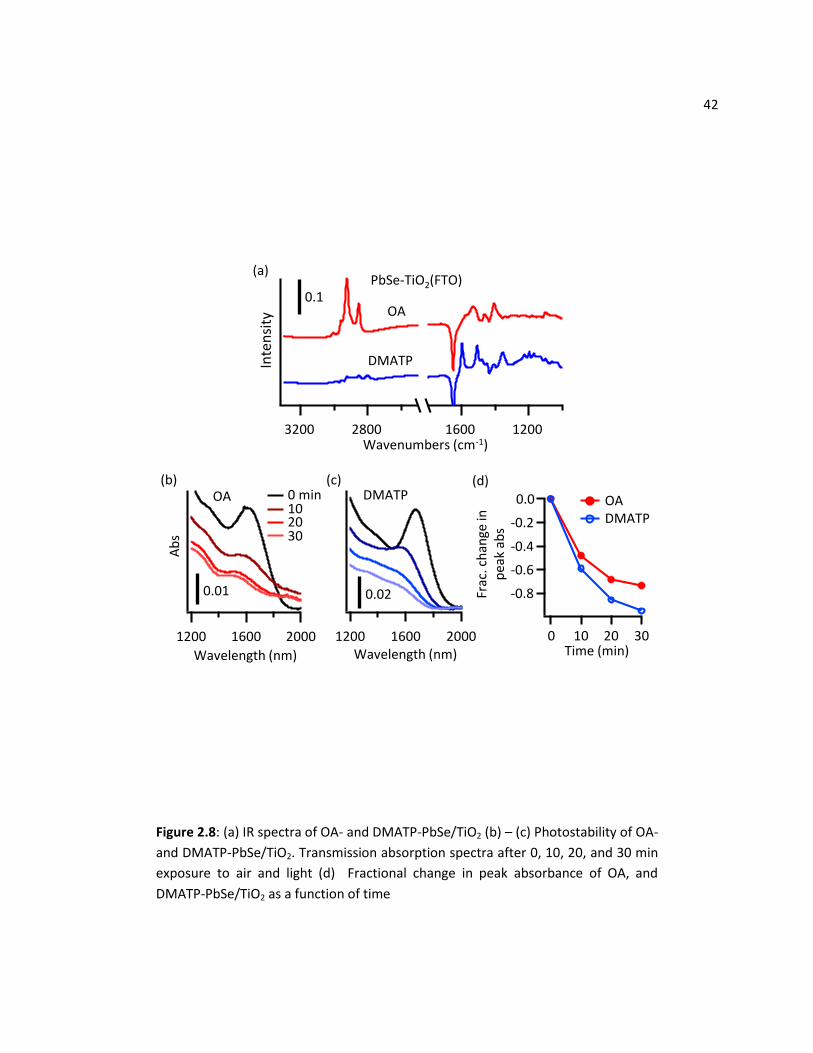
42
Figure 2.8: (a) IR spectra of OA- and DMATP-PbSe/TiO2 (b) – (c) Photostability of OA-
and DMATP-PbSe/TiO2. Transmission absorption spectra after 0, 10, 20, and 30 min
exposure to air and light (d) Fractional change in peak absorbance of OA, and
DMATP-PbSe/TiO2 as a function of time
0.1
Inte
nsi
ty
3200 2800Wavenumbers (cm-1)
1600 1200
OA
DMATP
PbSe-TiO2(FTO)
0.01
Ab
s
200016001200
Wavelength (nm)
OA 0 min102030
0.02
200016001200
DMATP
-0.8
-0.6
-0.4
-0.2
0.0Fr
ac. c
han
ge in
p
eak
abs
3020100Time (min)
OADMATP
Wavelength (nm)
(a)
(b) (c) (d)
43 2.7 Conclusions
Our results show that aromatic ligands bearing electron-donating substituents can provide
excellent protection of CdSe QDs against water and air oxidation during illumination when
functionalized on a QD sensitized TiO2. By stabilizing the sulfur end of the molecule with electron
donating groups, these small molecules can shuttle holes quickly and away from the thiol and the QD
surface, thus inhibiting oxidation of the QD and also providing protection for the interfacial thiol linker.
However, we found that DMATP ligands will desorb from the CdSe surface after a short cycling of a
liquid-junction solar cell. Lastly, in utilizing this ligand passivation idea, the positions of the ligand HOMO
level and QD VB must be such that the ligand is energetically able to accept the holes from the QD.
2.8 References
1. Kamat, P. V. Quantum Dot Solar Cells. Semiconductor Nanocrystals as Light Harvesters, J. Phys. Chem. C 2008, 112, 18737-18753.
2. Hodes, G. Comparison of Dye- and Semiconductor-Sensitized Porous Nanocrystalline Liquid Junction Solar Cells, J. Phys. Chem. C 2008, 112, 17778-17787.
3. Nozik, A. J. Quantum Dot Solar Cells, Physica E 2002, 14, 115-120.
4. Kongkanand, A.; Tvrdy, K.; Takechi, K.; Kuno, M.; Kamat, P. V. Quantum Dot Solar Cells. Tuning Photoresponse through Size and Shape Control of CdSe-TiO2 Architecture, J. Am. Chem. Soc. 2008, 130, 4007-4015.
5. Choi, J. J.; Lim, Y.-F.; Santiago-Berrios, M. E. B.; Oh, M.; Hyun, B.-R.; Sung, L.; Bartnik, A. C.; Goedhart, A.; Malliaras, G. G.; Abruna, H. D.; et al. PbSe Nanocrystal Excitonic Solar Cells, Nano Lett. 2009, 9, 3749-3755.
6. Canovas, E.; Moll, P.; Jensen, S. A.; Gao, Y.; Houtepen, A. J.; Siebbeles, L. D. A.; Kinge, S.; Bonn, M. Size-Dependent Electron Transfer from PbSe Quantum Dots to SnO2 Monitored by Picosecond Terahertz Spectroscopy, Nano Lett. 2011, 11, 5234-5239.
7. Pandey, A.; Guyot-Sionnest, P. Hot Electron Extraction From Colloidal Quantum Dots, J. Phys. Chem. Lett. 2010, 1, 45-47.
8. Tisdale, W. A.; Williams, K. J.; Timp, B. A.; Norris, D. J.; Aydil, E. S.; Zhu, X. Y. Hot-Electron Transfer from Semiconductor Nanocrystals, Science 2010, 328, 1543-1547.
44 9. Schaller, R. D.; Klimov, V. I. High Efficiency Carrier Multiplication in PbSe Nanocrystals:
Implications for Solar Energy Conversion, Phys. Rev. Lett. 2004, 92.
10. Califano, M.; Zunger, A.; Franceschetti, A. Efficient Inverse Auger Recombination at Threshold in CdSe Nanocrystals, Nano Lett. 2004, 4, 525-531.
11. Sambur, J. B.; Novet, T.; Parkinson, B. A. Multiple Exciton Collection in a Sensitized Photovoltaic System, Science 2010, 330, 63-66.
12. Semonin, O. E.; Luther, J. M.; Choi, S.; Chen, H.-Y.; Gao, J.; Nozik, A. J.; Beard, M. C. Peak External Photocurrent Quantum Efficiency Exceeding 100% via MEG in a Quantum Dot Solar Cell, Science 2011, 334, 1530-1533.
13. Barea, E. M.; Shalom, M.; Gimenez, S.; Hod, I.; Mora-Sero, I.; Zaban, A.; Bisquert, J. Design of Injection and Recombination in Quantum Dot Sensitized Solar Cells, J. Am. Chem. Soc. 2010, 132, 6834-6839.
14. Selinsky, R. S.; Shin, S.; Lukowski, M. A.; Jin, S. Epitaxial Heterostructures of Lead Selenide Quantum Dots on Hematite Nanowires, J. Phys. Chem. Lett. 2012, 3, 1649-1656.
15. Hyun, B. R.; Zhong, Y. W.; Bartnik, A. C.; Sun, L. F.; Abruna, H. D.; Wise, F. W.; Goodreau, J. D.; Matthews, J. R.; Leslie, T. M.; Borrelli, N. F. Electron Injection from Colloidal PbS Quantum Dots into Titanium Dioxide Nanoparticles, ACS Nano 2008, 2, 2206-2212.
16. Hoyer, P.; Konenkamp, R. Photoconduction in Porous TiO2 Sensitized by PbS Quantum Dots, Appl. Phys. Lett. 1995, 66, 349-351.
17. Tvrdy, K.; Kamat, P. V. Substrate Driven Photochemistry of CdSe Quantum Dot Films: Charge Injection and Irreversible Transformations on Oxide Surfaces, J. Phys. Chem. A 2009, 113, 3765-3772.
18. Zidek, K.; Zheng, K.; Chabera, P.; Abdellah, M.; Pullerits, T. Quantum Dot Photodegradation Due to CdSe-ZnO Charge Transfer: Transient Absorption Study, Appl. Phys. Lett. 2012, 100.
19. Sykora, M.; Koposov, A. Y.; McGuire, J. A.; Schulze, R. K.; Tretiak, O.; Pietryga, J. M.; Klimov, V. I. Effect of Air Exposure on Surface Properties, Electronic Structure, and Carrier Relaxation in PbSe Nanocrystals, ACS Nano 2010, 4, 2021-2034.
20. Katari, J. E. B.; Colvin, V. L.; Alivisatos, A. P. X-ray Photoelectron Spectroscopy of CdSe Nanocrystals with Applications to Studies of the Nanocrystal Surface, J. Phys. Chem. 1994, 98, 4109-4117.
21. Block, S. B.; Yurs, L. A.; Pakoulev, A. V.; Selinsky, R. S.; Jin, S.; Wright, J. C. Multiresonant Multidimensional Spectroscopy of Surface-Trapped Excitons in PbSe Quantum Dots, J. Phys. Chem. Lett 2012, 3, 2707-2712.
22. Ihly, R.; Tolentino, J.; Liu, Y.; Gibbs, M.; Law, M. The Photothermal Stability of PbS Quantum Dot Solids, ACS Nano 2011, 5, 8175-8186.
45 23. Guo, J.; She, C.; Lian, T. Effect of Insulating Oxide Overlayers on Electron Injection Dynamics in
Dye-Sensitized Nanocrystalline Thin Films, J. Phys. Chem. C 2007, 111, 8979-8987.
24. Brennan, T. P.; Bakke, J. R.; Ding, I. K.; Hardin, B. E.; Nguyen, W. H.; Mondal, R.; Bailie, C. D.; Margulis, G. Y.; Hoke, E. T.; Sellinger, A.; et al. The Importance of Dye Chemistry and TiCl4 Surface Treatment in the Behavior of Al2O3 Recombination Barrier Layers Deposited by Atomic Layer Deposition in Solid-State Dye-Sensitized Solar Cells, Phys. Chem. Chem. Phys. 2012, 14, 12130-12140.
25. Hung, L. S.; Chen, C. H. Recent Progress of Molecular Organic Electroluminescent Materials and Devices, Mater. Sci. Eng. R-Rep. 2002, 39, 143-222.
26. Shirota, Y.; Kageyama, H. Charge Carrier Transporting Molecular Materials and Their Applications in Devices, Chem. Rev. 2007, 107, 953-1010.
27. Yella, A.; Lee, H. W.; Tsao, H. N.; Yi, C. Y.; Chandiran, A. K.; Nazeeruddin, M. K.; Diau, E. W. G.; Yeh, C. Y.; Zakeeruddin, S. M.; Gratzel, M. Porphyrin-Sensitized Solar Cells with Cobalt (II/III)-Based Redox Electrolyte Exceed 12 Percent Efficiency, Science 2011, 334, 629-634.
28. Kitamura, T.; Ikeda, M.; Shigaki, K.; Inoue, T.; Anderson, N. A.; Ai, X.; Lian, T. Q.; Yanagida, S. Phenyl-Conjugated Oligoene Sensitizers for TiO2 Solar Cells, Chem. Mater. 2004, 16, 1806-1812.
29. Zhang, W.; Fang, Z.; Su, M. J.; Saeys, M.; Liu, B. A Triphenylamine-Based Conjugated Polymer with Donor-pi-Acceptor Architecture as Organic Sensitizer for Dye-Sensitized Solar Cells, Macromol. Rapid Commun. 2009, 30, 1533-1537.
30. Ito, S.; Murakami, T. N.; Comte, P.; Liska, P.; Gratzel, C.; Nazeeruddin, M. K.; Gratzel, M. Fabrication of Thin Film Dye Sensitized Solar Cells with Solar to Electric Power Conversion Efficiency Over 10%, Thin Solid Films 2008, 516, 4613-4619.
31. Peng, Z. A.; Peng, X. G. Formation of High-Quality CdTe, CdSe, and CdS Nanocrystals using CdO as Precursor, J. Am. Chem. Soc. 2001, 123, 183-184.
32. Yu, W. W.; Qu, L. H.; Guo, W. Z.; Peng, X. G. Experimental Determination of the Extinction Coefficient of CdTe, CdSe, and CdS Nanocrystals, Chem. Mater. 2003, 15, 2854-2860.
33. Sambur, J. B.; Riha, S. C.; Choi, D.; Parkinson, B. A. Influence of Surface Chemistry on the Binding and Electronic Coupling of CdSe Quantum Dots to Single Crystal TiO2 Surfaces, Langmuir 2010, 26, 4839-4847.
34. Pernik, D. R.; Tvrdy, K.; Radich, J. G.; Kamat, P. V. Tracking the Adsorption and Electron Injection Rates of CdSe Quantum Dots on TiO2: Linked versus Direct Attachment, J. Phys. Chem. C 2011, 115, 13511-13519.
35. Guijarro, N.; Lana-Villarreal, T.; Mora-Sero, I.; Bisquert, J.; Gomez, R. CdSe Quantum Dot-Sensitized TiO2 Electrodes: Effect of Quantum Dot Coverage and Mode of Attachment, J. Phys. Chem. C 2009, 113, 4208-4214.

46 36. Gaussian 09, Revision C.01. Frisch, M. J.; Trucks, G. W.; Schlegel, H. B.; Scuseria, G. E.; Robb, M.
A.; Cheeseman, J. R.; Scalmani, G.; Barone, V.; Mennucci, B.; Petersson, G. A.; et al., Gaussian, Inc., Wallingford CT, 2010.
37. Dunning, T. H., Jr.; Hay, P. J. Modern Theoretical Chemistry; Plenum: New York; 1976; Vol. 3; pp 1-28.
38. NBO 5.9. Glendening, E. D.; Badenhoop, J. K.; Reed, A. E.; Carpenter, J. E.; Bohmann, J. A.; Morales, C. M.; Weinhold, F., (Theoretical Chemistry Institute, University of Wisconsin, Madison, WI, 2012); http://www.chem.wisc.edu/~nbo5.
39. Feldt, S. M.; Gibson, E. A.; Gabrielsson, E.; Sun, L.; Boschloo, G.; Hagfeldt, A. Design of Organic Dyes and Cobalt Polypyridine Redox Mediators for High-Efficiency Dye-Sensitized Solar Cells, J. Am. Chem. Soc. 2010, 132, 16714-16724.
40. Young, A. G.; Al-Salim, N.; Green, D. P.; McQuillan, A. J. Attenuated Total Reflection Infrared Studies of Oleate and Trioctylphosphine Oxide Ligand Adsorption and Exchange Reactions on CdS Quantum Dot Films, Langmuir 2008, 24, 3841-3849.
41. Hamizi, N. A.; Johan, M. R. Synthesis and Size Dependent Optical Studies in CdSe Quantum Dots via Inverse Micelle Technique, Mater. Chem. Phys. 2010, 124, 395-398.
42. Rajalingam, K.; Hallmann, L.; Strunskus, T.; Bashir, A.; Woll, C.; Tuczek, F. Self-Assembled Monolayers of Benzylmercaptan and Para-cyanobenzylmercaptan on Gold: Surface Infrared Spectroscopic Characterization, Phys. Chem. Chem. Phys. 2010, 12, 4390-4399.
43. Shukla, A. R.; Asthana, B. P.; Dongre, N. G.; Pathak, C. M. Infrared and Raman-Spectra of Non-vicinaly Trisubstituted 2,5-Dimethylaniline and 2-Methyl-5-chloroaniline, Vib. Spectrosc. 1992, 3, 245-253.
44. Porter, M. D.; Bright, T. B.; Allara, D. L.; Chidsey, C. E. D. Spontaneously Organized Molecular Assemblies. 4. Structural Characterization of Normal-Alkyl Thiol Monolayers on Gold by Optical Ellipsometry, Infrared-Spectroscopy, and Electrochemistry, J. Am. Chem. Soc. 1987, 109, 3559-3568.
45. Aldana, J.; Wang, Y. A.; Peng, X. G. Photochemical Instability of CdSe Nanocrystals Coated by Hydrophilic Thiols, J. Am. Chem. Soc. 2001, 123, 8844-8850.
46. Yu, W. W.; Wang, Y. A.; Peng, X. G. Formation and Stability of Size-, Shape-, and Structure-Controlled CdTe Nanocrystals: Ligand Effects on Monomers and Nanocrystals, Chem. Mater. 2003, 15, 4300-4308.
47. Wuister, S. F.; Donega, C. D.; Meijerink, A. Influence of Thiol Capping on the Exciton Luminescence and Decay Kinetics of CdTe and CdSe Quantum Dots, J. Phys. Chem. B 2004, 108, 17393-17397.
48. Bullen, C.; Mulvaney, P. The Effects of Chemisorption on the Luminescence of CdSe Quantum Dots, Langmuir 2006, 22, 3007-3013.
47 49. Munro, A. M.; Jen-La Plante, I.; Ng, M. S.; Ginger, D. S. Quantitative Study of the Effects of
Surface Ligand Concentration on CdSe Nanocrystal Photoluminescence, J. Phys. Chem. C 2007, 111, 6220-6227.
50. Koole, R.; Schapotschnikow, P.; Donega, C. d. M.; Vlugt, T. J. H.; Meijerink, A. Time-Dependent Photoluminescence Spectroscopy as a Tool to Measure the Ligand Exchange Kinetics on a Quantum Dot Surface, ACS Nano 2008, 2, 1703-1714.
51. Liu, I. S.; Lo, H.-H.; Chien, C.-T.; Lin, Y.-Y.; Chen, C.-W.; Chen, Y.-F.; Su, W.-F.; Liou, S.-C. Enhancing Photoluminescence Quenching and Photoelectric Properties of CdSe Quantum Dots with Hole Accepting Ligands, J. Mater. Chem. 2008, 18, 675-682.
52. Ning, Z.; Molnar, M.; Chen, Y.; Friberg, P.; Gan, L.; Agren, H.; Fu, Y. Role of Surface Ligands in Optical Properties of Colloidal CdSe/CdS Quantum Dots, Phys. Chem. Chem. Phys. 2011, 13, 5848-5854.
53. Bawendi, M. G.; Carroll, P. J.; Wilson, W. L.; Brus, L. E. Luminescence Properties of CdSe Quantum Crystallites - Resonance between Interior and Surface Localized States, J. Chem. Phys. 1992, 96, 946-954.
54. Javier, A.; Magana, D.; Jennings, T.; Strouse, G. F. Nanosecond Exciton Recombination Dynamics in Colloidal CdSe Quantum Dots under Ambient Conditions, Appl. Phys. Lett. 2003, 83, 1423-1425.
55. Burda, C.; Link, S.; Mohamed, M.; El-Sayed, M. The Relaxation Pathways of CdSe Nanoparticles Monitored with Femtosecond Time-Resolution from the Visible to the IR: Assignment of the Transient Features by Carrier Quenching, J. Phys. Chem. B 2001, 105, 12286-12292.
56. Huang, J. E.; Huang, Z. Q.; Jin, S. Y.; Lian, T. Q. Exciton Dissociation in CdSe Quantum Dots by Hole Transfer to Phenothiazine, J. Phys. Chem. C 2008, 112, 19734-19738.
57. Hamel, S.; Duffy, P.; Casida, M. E.; Salahub, D. R. Kohn-Sham Orbitals and Orbital Energies: Fictitious Constructs but Good Approximations All the Same, J. Electron Spectrosc. Relat. Phenom. 2002, 123, 345-363.
58. Shankar, R.; Senthilkumar, K.; Kolandaivel, P. Calculation of Ionization Potential and Chemical Hardness: A Comparative Study of Different Methods, Int. J. Quantum Chem. 2009, 109, 764-771.
59. Rempel, J. Y.; Trout, B. L.; Bawendi, M. G.; Jensen, K. F. Density Functional Theory Study of Ligand Binding on CdSe (0001), (000(1)over-bar), and (11(2)over-bar-0) Single Crystal Relaxed and Reconstructed Surfaces: Implications for Nanocrystalline Growth, J. Phys. Chem. B 2006, 110, 18007-18016.
60. Yang, P.; Tretiak, S.; Ivanov, S. Influence of Surfactants and Charges on CdSe Quantum Dots, J. Cluster Sci. 2011, 22, 405-431.
48 61. Sadlej-Sosnowska, N.; Krygowski, T. M. Substituent Effect on Geometry of the NO and
N(CH(3))(2) Groups in Para Substituted Derivatives of Nitrosobenzene and N,N-Dimethylaniline, Chem. Phys. Lett. 2009, 476, 191-195.
62. Wang, B. C.; Liao, H. R.; Chang, J. C.; Chen, L.; Yeh, J. T. Electronic Structure and Molecular Orbital Study of Hole-Transport Material Triphenylamine Derivatives, J. Lumin. 2007, 124, 333-342.
63. Smith, A. M.; Duan, H.; Rhyner, M. N.; Ruan, G.; Nie, S. A Systematic Examination of Surface Coatings on the Optical and Chemical Properties of Semiconductor Quantum Dots, Phys. Chem. Chem. Phys. 2006, 8, 3895-3903.
64. Liang, Y.; Thorne, J. E.; Parkinson, B. A. Controlling the Electronic Coupling between CdSe Quantum Dots and Thiol Capping Ligands via pH and Ligand Selection, Langmuir 2012.
65. Mulvihill, M. J.; Habas, S. E.; Jen-La Plante, H.; Wan, J.; Mokari, T. Influence of Size, Shape, and Surface Coating on the Stability of Aqueous Suspensions of CdSe Nanoparticles, Chem. Mater. 2010, 22, 5251-5257.
66. Xi, L.; Lek, J. Y.; Liang, Y. N.; Boothroyd, C.; Zhou, W.; Yan, Q.; Hu, X.; Chiang, F. B. Y.; Lam, Y. M. Stability studies of CdSe Nanocrystals in an Aqueous Environment, Nanotechnology 2011, 22.
67. Schapotschnikow, P.; Hommersom, B.; Vlugt, T. J. H. Adsorption and Binding of Ligands to CdSe Nanocrystals, J. Phys. Chem. C 2009, 113, 12690-12698.
68. Gomes, R.; Hassinen, A.; Szczygiel, A.; Zhao, Q.; Vantomme, A.; Martins, J. C.; Hens, Z. Binding of Phosphonic Acids to CdSe Quantum Dots: A Solution NMR Study, J. Phys. Chem. Lett. 2011, 2, 145-152.
69. Wang, F.; Buhro, W. E. Morphology Control of Cadmium Selenide Nanocrystals: Insights into the Roles of Di-n-octylphosphine Oxide (DOPO) and Di-n-octylphosphinic Acid (DOPA), J. Am. Chem. Soc. 2012, 134, 5369-5380.
70. Frederick, M. T.; Weiss, E. A. Relaxation of Exciton Confinement in CdSe Quantum Dots by Modification with a Conjugated Dithiocarbamate Ligand, ACS Nano 2010, 4, 3195-3200.
71. Sengar, R. S.; Nemykin, V. N.; Basu, P. Electronic Properties of Para-Substituted Thiophenols and Disulfides from C-13 NMR Spectroscopy and Ab Initio Calculations: Relations to the Hammett Parameters and Atomic Charges, New J. Chem. 2003, 27, 1115-1123.
72. Okamoto, Y.; Brown, H. C. A Quantitative Treatment for Electrophilic Reactions of Aromatic Derivatives, J. Org. Chem. 1957, 22, 485-494.
73. Colvin, V. L.; Schlamp, M. C.; Alivisatos, A. P. Light-Emitting-Diodes Made From Cadmium Selenide Nanocrystals And A Semiconducting Polymer, Nature 1994, 370, 354-357.

49 74. McDonald, S. A.; Konstantatos, G.; Zhang, S. G.; Cyr, P. W.; Klem, E. J. D.; Levina, L.; Sargent, E. H.
Solution-Processed PbS Quantum Dot Infrared Photodetectors and Photovoltaics, Nat. Mater. 2005, 4, 138-U114.
75. Fafarman, A. T.; Koh, W. K.; Diroll, B. T.; Kim, D. K.; Ko, D. K.; Oh, S. J.; Ye, X. C.; Doan-Nguyen, V.; Crump, M. R.; Reifsnyder, D. C.; et al. Thiocyanate-Capped Nanocrystal Colloids: Vibrational Reporter of Surface Chemistry and Solution-Based Route to Enhanced Coupling in Nanocrystal Solids, J. Am. Chem. Soc. 2011, 133, 15753-15761.
76. Kovalenko, M. V.; Scheele, M.; Talapin, D. V. Colloidal Nanocrystals with Molecular Metal Chalcogenide Surface Ligands, Science 2009, 324, 1417-1420.
77. Law, M.; Luther, J. M.; Song, O.; Hughes, B. K.; Perkins, C. L.; Nozik, A. J. Structural, Optical, and Electrical Properties of PbSe Nanocrystal Solids Treated Thermally or with Simple Amines, J. Am. Chem. Soc. 2008, 130, 5974-5985.
78. Leatherdale, C. A.; Kagan, C. R.; Morgan, N. Y.; Empedocles, S. A.; Kastner, M. A.; Bawendi, M. G. Photoconductivity in CdSe Quantum Dot Solids, Phys. Rev. B 2000, 62, 2669-2680.
79. Lee, J. S.; Kovalenko, M. V.; Huang, J.; Chung, D. S.; Talapin, D. V. Band-like Transport, High Electron Mobility and High Photoconductivity in All-Inorganic Nanocrystal Arrays, Nat. Nanotechnol. 2011, 6, 348-352.
80. Hines, M. A.; Scholes, G. D. Colloidal PbS Nanocrystals with Size-Tunable Near-Infrared Emission: Observation of Post-Synthesis Self-Narrowing of the Particle Size Distribution, Adv. Mater. 2003, 15, 1844-1849.
81. Murray, C. B.; Sun, S. H.; Gaschler, W.; Doyle, H.; Betley, T. A.; Kagan, C. R. Colloidal Synthesis of Nanocrystals and Nanocrystal Superlattices, IBM J. Res. & Dev. 2001, 45, 47-56.
82. Wehrenberg, B. L.; Wang, C. J.; Guyot-Sionnest, P. Interband and Intraband Optical Studies of PbSe Colloidal Quantum Dots, J. Phys. Chem. B 2002, 106, 10634-10640.
83. Cademartiri, L.; Montanari, E.; Calestani, G.; Migliori, A.; Guagliardi, A.; Ozin, G. A. Size-Dependent Extinction Coefficients of PbS Quantum Dots, J. Am. Chem. Soc. 2006, 128, 10337-10346.
84. Dai, Q.; Wang, Y.; Li, X.; Zhang, Y.; Pellegrino, D. J.; Zhao, M.; Zou, B.; Seo, J.; Wang, Y.; Yu, W. W. Size-Dependent Composition and Molar Extinction Coefficient of PbSe Semiconductor Nanocrystals, ACS Nano 2009, 3, 1518-1524.
85. Moreels, I.; Lambert, K.; Smeets, D.; De Muynck, D.; Nollet, T.; Martins, J. C.; Vanhaecke, F.; Vantomme, A.; Delerue, C.; Allan, G.; et al. Size-Dependent Optical Properties of Colloidal PbS Quantum Dots, ACS Nano 2009, 3, 3023-3030.
86. Jasieniak, J.; Califano, M.; Watkins, S. E. Size-Dependent Valence and Conduction Band-Edge Energies of Semiconductor Nanocrystals, ACS Nano 2011, 5, 5888-5902.

50
Chapter 3
Photostability of CdSe Quantum Dots Functionalized with Conjugated
Dithiocarbamates
3.1 Introduction
Chalcogenide quantum dots (QDs) have the potential as the photoactive material in sensitized
solar cells1 and other optical devices2-4 but are prone to photodegradation from water and air.5-8 Various
conventional methods have been utilized to passivate the surface, including large-bandgap shells,9,10
long hydrophobic hydrocarbon chains11 and organic polymer encapsulation.12,13 When using organic
ligands to passivate QDs, short conductive ligands are more desirable for QD applications that require
electrical transport such as in photodetectors, photovoltaic devices, and QD-LEDs.14,15 Conductive
organic ligands significantly affect the QD surface electronic structure16-18 and could play a significant
role in controlling the QD photostability.19
Of the conventional ligands for synthesis and manipulation of QDs, thiols are widely used, as
thiols thermodynamically bind more strongly than other common ligands such as carboxylic acids,
phosphonic acids, and amines.20 However, thiols still have inherent problems with photooxidation21 and
labile surface chemistry.22 Bidentate ligands with two chelating sulfur groups are promising functional
groups enhance the binding to QDs,23,24 one of which is the dithiocarbamate (DTC) group (R-NHCS2-)
Although bidentate ligands are expected to bind more strongly to the QD, there is some evidence that
bidentate binding may not necessarily lead to more stable QDs;21,25 more studies are needed to
determine whether there is a relationship between chelating ligand attachment and QD photostability.
Current methods to attach DTC ligands to CdSe QD surfaces involve the separate synthesis of
the ligand molecule or a purification step of the QDs.17,26,27 DTC molecules have been functionalized in-
situ on gold surfaces, under mildly basic conditions.28,29 In this chapter, we discuss the successful in-situ
51 functionalization of DTC molecules on CdSe-TiO2 films, and the utilization of this chemistry to explore
the effect of this bidentate DTC group attachment on QD photostability. With a series of para-
substituted conjugated DTC ligands, we show the increase in QD photostability trended with the
increase in electron-donating ability of the substituent. Finally, we compare the effect of the bidendate
DTC vs. a monodentate thiol on QD photostability.
3.2 Experimental
3.2.1 Chemicals
Trioctylphosphine oxide (TOPO, 99+%), CdO (99.99+% metal basis), oleic acid (OA, 90%),
trioctylphosphine (TOP, 90%), selenium, (99.99% metal basis), 4-(trifluoromethoxy)aniline( 98%), aniline
(≥99%), p-anisidine (≥99%), N,N-dimethyl-p-phenylenediamine (97%), carbon disulfide (anhydrous,
≥99%), triethylamine (TEA, ≥99.5%),and 4-methoxythiophenol (97%) were purchased from Sigma-
Aldrich and used without further purification.
3.2.2 Preparation of TiO2 Nanocrystalline Films
Fluorine-doped tin oxide (FTO) coated glass (Hartford glass) was cleaned with detergent,
acetone, and ethanol. Porous anatase nanocrystalline TiO2 films were then screen-printed onto the FTO
glass from a commercially available paste (Solaronix T/SP). Each pass of the screen-printing process
produced layers of approximately 1 μm thick. The screen printing process also produced multiple
samples of the same thickness and mesoporous structure, and each experiment in this work was
conducted with the same batch of films. After the screen-printing step, the TiO2 films were then
annealed in air using a recipe adapted from literature:30 at 325 C for 5 min, at 375 C for 5 min, at 450
C for 15 min, and finally at 500 C for 30 min. Before use, the films were cleaned by heating them at
500 C for 15 min in air to remove any additional organic contaminants. For XPS and FTIR studies, thin
films from one screen-print pass were used. Thicker films resulted in interference effects in the FTIR
spectra. For photostability studies with UV-visible spectroscopy, films from two passes were used; the
52 higher optical densities obtained resulting from increased CdSe QD loading gave better comparisons
among ligands.
3.2.3 Synthesis of CdSe QDs
The QDs were synthesized using a procedure adapted from Peng and Peng.31 First, 3.1 g TOPO,
0.24 g CdO, and 1.9 g OA were combined in a three-necked flask and heated in an Ar atmosphere until
the mixture turned optically clear (~290 C). The mixture was allowed to cool until ~250 C and a
solution of TOPSe (made from 1.2 mL TOP and 0.045 g Se) was quickly injected. The temperature
dropped to 220-230 C after injection and the formed QDs were allowed to cool to ~80 C. The QDs
were quenched with toluene and purified four times by precipitation using methanol and centrifugation.
The size and concentration of the QDs were determined by UV-visible spectroscopy from the
wavelength and absorbance of the first exciton peak, using empirical relationships established by Yu et
al.32 Typically, the QDs from this synthesis procedure were 3 – 3.2 nm in diameter.
3.2.4 CdSe-TiO2 Preparation and Ligand Modification
The CdSe QDs were attached to the TiO2 by directly immersing a clean TiO2 film into a solution
of QDs for 24 h. Although using a linker may give more control over QD coverage, studies have shown
reduced electron transfer rate from the linked heterostructures.33-35 Furthermore, commonly used
linkers like mercapto-alkanoic acids contain sulfur and the lack of these sulfur containing linkers on our
CdSe-TiO2 samples made FTIR and XPS characterization of the DTC functionalization more convenient.
To prepare the CdSe-TiO2 surfaces the TiO2 films were immersed in 15 – 25 μM (defined as moles of
CdSe QD per liter) solution in dichloromethane (DCM)33 for 24 h, then rinsed with DCM and dried with
N2. To further functionalize these films with DTC molecules, the films were immersed in a stirred, Ar-
degassed solution of 50 mM R-aniline, 50 mM CS2, and 50 mM TEA in methanol for 4 h in the dark. They
were then rinsed thoroughly with methanol and dried. To functionalize the CdSe-TiO2 with 4-

53 methoxythiophenol (MeO-Ph-SH), the films were similarly immersed in an Ar-degassed 50 mM solution
of MeO-Ph-SH in methanol for 4 h, then rinsed with methanol and dried.
3.2.5 Fourier-Transform Infrared Spectroscopy (FTIR)
FTIR characterization of the functionalized CdSe-TiO2 films was performed in single bounce
reflection mode with a Vertex 70 (Bruker) with p-polarized light at an incident angle of 50o from sample
normal. An identically prepared bare TiO2 film served as the reference spectra for each experiment, and
the functionalized samples were measured immediately after the reference. This method minimized the
effect of atmospheric water and CO2. Reference spectra of the parent aniline were measured in
transmission mode on ZnSe plates. All measurements were done at a resolution of 4 cm-1.
3.2.6 X-ray Photoelectron Spectroscopy (XPS)
We performed XPS measurements with a custom-built XPS system (Physical Electronics) with an
Al-Kα source (Model 10-610, 1486.6 eV photon energy), toroidal monochromator (Model 10-420), and
hemispherical analyzer with a 16 channel detector array (Model 10-360). Measurements were done at
an electron take-off angle of 45 with a resolution of 0.1 eV. The resulting XPS peaks were fit to a Voigt
function to obtain peak areas.
3.2.7 Water Photostability Studies
Samples were sandwiched into a custom-made cell with a Teflon spacer (127 μm thick) and
another piece of FTO. The open region as defined by the spacer was filled with 18 MΩ H2O (Barnstead
Nanopure). The cell has holes to allow for light penetration and absorption measurement without
disassembly. Samples were illuminated through the FTO piece and water with light from a solar
simulator after passing through a filter that only allows transmission of wavelengths longer than 475
nm. The solar simulator (Newport 91160) was equipped with AM1.5G filters and set to 100 mW/cm2 (as
measured by a Scientech calorimeter). The light after the filter was measured to be 81 mW/cm2. We
used the filter to ensure that the light could only be absorbed by the CdSe QDs, and not the TiO2.
54 Transmission measurements using a UV-visible spectrometer (Shimadzu UV-2401PC) were taken at
various time points of light exposure.
3.2.8 Photoluminescence (PL)
We prepared solution-based QDs functionalized with DTC ligands for the PL experiments. The
CdSe QDs were precipitated, centrifuged and resuspended in chloroform. R-aniline and CS2 were added
into the solution at a concentration of 50 mM each and the entire mixture was stirred in the dark for 4
h. To get rid of excess starting reagents, the QD mixture was precipitated with methanol, and
resuspended with chloroform. PL experiments were done at a concentration of 1.5 μM with a
flourometer (ISS K2) with 450 nm as the excitation wavelength.
3.3 Results
3.3.1 FTIR and XPS Characterization
As a start, we functionalized the CdSe-TiO2 surfaces using an aniline with a fluorine containing
substituent: OCF3-aniline. The CF3 group serves as a molecular tag since it has relatively unique
absorption features in the IR at ~1200-1300 cm-1 and the F(1s) region in the XPS also does not overlap
with any other regions present on the spectra. Figure 3.1 shows IR and XPS spectra of the resulting
functionalization of DTC after a 4 h reaction along with the proper control experiments. The unmodified
sample shows carboxylate stretches at 1535 and 1412 cm-1 resulting from oleate capped QDs.36 When
the CdSe-TiO2 sample was exposed to both OCF3-aniline and CS2 the carboxylate peaks disappeared and
we observed new peaks at 1510, 1271, and 1227 cm-1. As a reference, the IR spectrum of neat OCF3-
aniline is included. Prominent peaks of this neat liquid occur at 1350 – 1150 cm-1 and 1510 cm-1,
characteristic of the –CF3 and the aromatic C=C stretches respectively. The peaks of the reacted samples
correspond to those of the parent compound, with a slight change of the peak shape in the CF3 region.
Leaving out the CS2 showed that the aniline compound itself does not bind onto the CdSe surface, as
shown in the IR of ‘No CS2’ sample. Exposure of reactants to a bare TiO2 surface also resulted in no
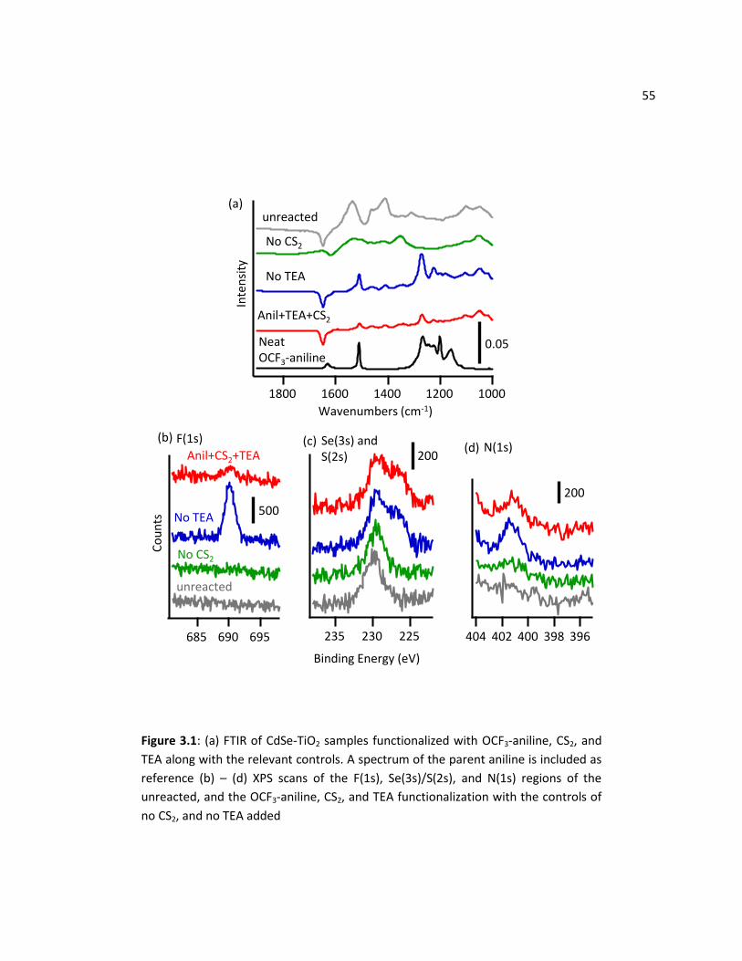
55
F(1s) Se(3s) andS(2s)
1800 1600 1400 1200 1000
Neat OCF3-aniline
Anil+TEA+CS2
No TEA
No CS2
unreacted
Wavenumbers (cm-1)
0.05
Inte
nsi
ty
(a)
Co
un
ts
695690685
Anil+CS2+TEA
No TEA
No CS2
unreacted
500
200
235 230 225
Binding Energy (eV)
200
404 402 400 398 396
N(1s)(b) (c)
(d)
Figure 3.1: (a) FTIR of CdSe-TiO2 samples functionalized with OCF3-aniline, CS2, and
TEA along with the relevant controls. A spectrum of the parent aniline is included as
reference (b) – (d) XPS scans of the F(1s), Se(3s)/S(2s), and N(1s) regions of the
unreacted, and the OCF3-aniline, CS2, and TEA functionalization with the controls of
no CS2, and no TEA added
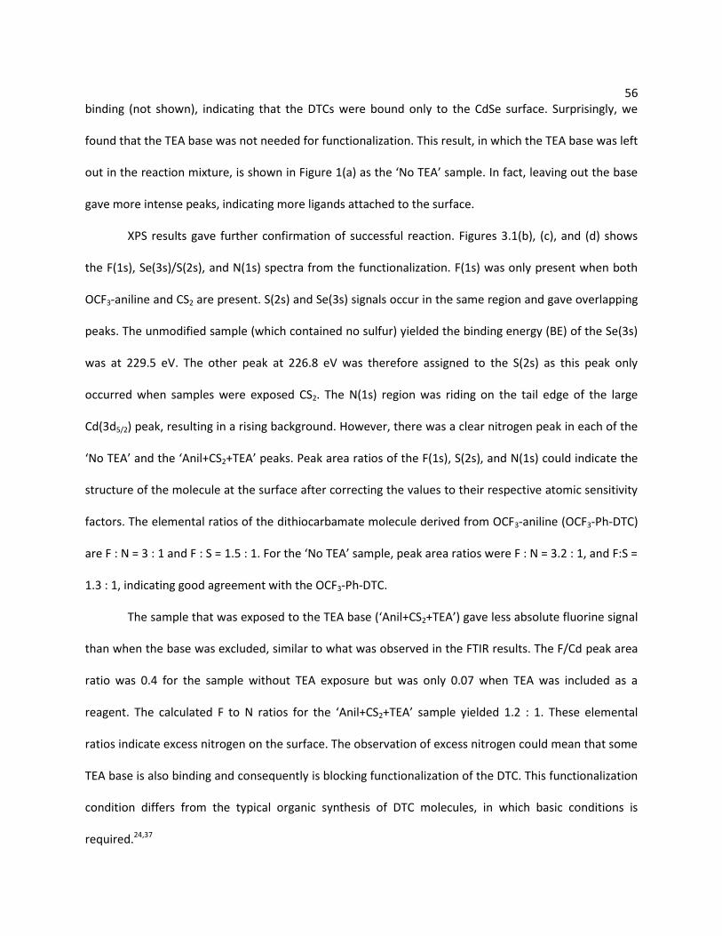
56 binding (not shown), indicating that the DTCs were bound only to the CdSe surface. Surprisingly, we
found that the TEA base was not needed for functionalization. This result, in which the TEA base was left
out in the reaction mixture, is shown in Figure 1(a) as the ‘No TEA’ sample. In fact, leaving out the base
gave more intense peaks, indicating more ligands attached to the surface.
XPS results gave further confirmation of successful reaction. Figures 3.1(b), (c), and (d) shows
the F(1s), Se(3s)/S(2s), and N(1s) spectra from the functionalization. F(1s) was only present when both
OCF3-aniline and CS2 are present. S(2s) and Se(3s) signals occur in the same region and gave overlapping
peaks. The unmodified sample (which contained no sulfur) yielded the binding energy (BE) of the Se(3s)
was at 229.5 eV. The other peak at 226.8 eV was therefore assigned to the S(2s) as this peak only
occurred when samples were exposed CS2. The N(1s) region was riding on the tail edge of the large
Cd(3d5/2) peak, resulting in a rising background. However, there was a clear nitrogen peak in each of the
‘No TEA’ and the ‘Anil+CS2+TEA’ peaks. Peak area ratios of the F(1s), S(2s), and N(1s) could indicate the
structure of the molecule at the surface after correcting the values to their respective atomic sensitivity
factors. The elemental ratios of the dithiocarbamate molecule derived from OCF3-aniline (OCF3-Ph-DTC)
are F : N 3 : 1 and F : S 1.5 : 1. For the ‘No TEA’ sample, peak area ratios were F : N 3.2 : 1, and F:S
1.3 : 1, indicating good agreement with the OCF3-Ph-DTC.
The sample that was exposed to the TEA base (‘Anil+CS2+TEA’) gave less absolute fluorine signal
than when the base was excluded, similar to what was observed in the FTIR results. The F/Cd peak area
ratio was 0.4 for the sample without TEA exposure but was only 0.07 when TEA was included as a
reagent. The calculated F to N ratios for the ‘Anil+CS2+TEA’ sample yielded 1.2 : 1. These elemental
ratios indicate excess nitrogen on the surface. The observation of excess nitrogen could mean that some
TEA base is also binding and consequently is blocking functionalization of the DTC. This functionalization
condition differs from the typical organic synthesis of DTC molecules, in which basic conditions is
required.24,37
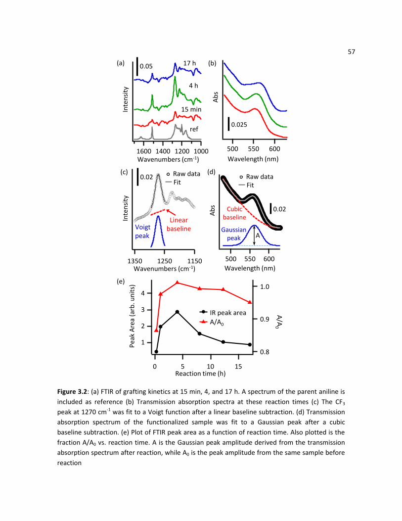
57
Figure 3.2: (a) FTIR of grafting kinetics at 15 min, 4, and 17 h. A spectrum of the parent aniline is
included as reference (b) Transmission absorption spectra at these reaction times (c) The CF3
peak at 1270 cm-1 was fit to a Voigt function after a linear baseline subtraction. (d) Transmission
absorption spectrum of the functionalized sample was fit to a Gaussian peak after a cubic
baseline subtraction. (e) Plot of FTIR peak area as a function of reaction time. Also plotted is the
fraction A/A0 vs. reaction time. A is the Gaussian peak amplitude derived from the transmission
absorption spectrum after reaction, while A0 is the peak amplitude from the same sample before
reaction
15 min
4 h
17 h
ref
0.05
1600 1400 1200 1000
Inte
nsi
ty0.025
600550500
Ab
s
0.02
1350 1250 1150
Raw dataFit
Voigtpeak
Linear baseline
0.02
600550500
Wavelength (nm)
Gaussian peak
Cubicbaseline
Raw dataFit
Ab
s
Inte
nsi
ty
Wavenumbers (cm-1)
Wavenumbers (cm-1) Wavelength (nm)
4
3
2
1Pea
k A
rea
(arb
. un
its)
151050Reaction time (h)
1.0
0.9
0.8
A/A
0
IR peak area
A/A0
(a) (b)
(c) (d)
(e)
A
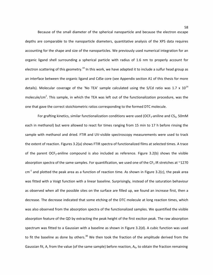
58 Because of the small diameter of the spherical nanoparticle and because the electron escape
depths are comparable to the nanoparticle diameters, quantitative analysis of the XPS data requires
accounting for the shape and size of the nanoparticles. We previously used numerical integration for an
organic ligand shell surrounding a spherical particle with radius of 1.6 nm to properly account for
electron scattering of this geometry.19 In this work, we have adapted it to include a sulfur head group as
an interface between the organic ligand and CdSe core (see Appendix section A1 of this thesis for more
details). Molecular coverage of the ‘No TEA’ sample calculated using the S/Cd ratio was 1.7 x 10¹⁴
molecule/cm2. This sample, in which the TEA was left out of the functionalization procedure, was the
one that gave the correct stoichiometric ratios corresponding to the formed DTC molecule.
For grafting kinetics, similar functionalization conditions were used (OCF3-aniline and CS2, 50mM
each in methanol) but were allowed to react for times ranging from 15 min to 17 h before rinsing the
sample with methanol and dried. FTIR and UV-visible spectroscopy measurements were used to track
the extent of reaction. Figures 3.2(a) shows FTIR spectra of functionalized films at selected times. A trace
of the parent OCF3-aniline compound is also included as reference. Figure 3.2(b) shows the visible
absorption spectra of the same samples. For quantification, we used one of the CF3 IR stretches at ~1270
cm-1 and plotted the peak area as a function of reaction time. As shown in Figure 3.2(c), the peak area
was fitted with a Voigt function with a linear baseline. Surprisingly, instead of the saturation behaviour
as observed when all the possible sites on the surface are filled up, we found an increase first, then a
decrease. The decrease indicated that some etching of the DTC molecule at long reaction times, which
was also observed from the absorption spectra of the functionalized samples. We quantified the visible
absorption feature of the QD by extracting the peak height of the first exciton peak. The raw absorption
spectrum was fitted to a Gaussian with a baseline as shown in Figure 3.2(d). A cubic function was used
to fit the baseline as done by others.38 We then took the fraction of the amplitude derived from the
Gaussian fit, A, from the value (of the same sample) before reaction, A0, to obtain the fraction remaining
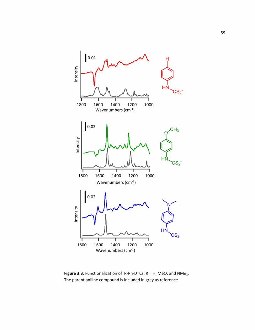
59
Figure 3.3: Functionalization of R-Ph-DTCs, R = H, MeO, and NMe2.
The parent aniline compound is included in grey as reference
Inte
nsi
ty
1800 1600 1400 1200 1000Wavenumbers (cm-1)
0.01
0.02
Inte
nsi
ty
1800 1600 1400 1200 1000
Wavenumbers (cm-1)
0.02
Inte
nsi
ty
1800 1600 1400 1200 1000Wavenumbers (cm-1)

60 or A/A0. The peak height, A was normalized to the peak height of the same sample before reaction, A0.
We plotted the A/A0 values as a function of time along with the FTIR peak area data in Figure 3.3(e). The
A/A0 values were observed to follow the same trend as the IR peak areas. At time < 4 h, the A/A0
increased as the peak evolved into the red-shifted DTC-QD. At optimal functionalization time (time=4 h),
the A/A0 became ~1. At longer times, the peak height decreased which might mean that some etching of
the QDs had occurred.
We further extended this surface functionalization to other para-substituted phenyl groups, R-
Ph-DTC, where R is either H, MeO, or NMe2. FTIR spectra of these samples are shown in Figure 3.3. All
reactions were done at the same concentrations (50 mM each of R-aniline and CS2 in methanol) without
the addition of TEA base, and at reaction time of 4 h. As observed from conducting DTC grafting kinetics
with R = OCF3 (discussed above), the DTC functionalization was optimal at this reaction time.
3.3.2 Water Photostability of R-Ph-DTCs Functionalized CdSe-TiO2
With the series of para-substituted R-Ph-DTC ligands on CdSe-TiO2, we investigated the
photostability of the QDs in water. Figure 3.4(a) shows the evolution of the transmission absorption of
the OCF3-Ph-DTC functionalized sample for up to a total of 10 min of light and water exposure. At 0 min,
we observed a peak at 559 nm corresponding to the first exciton peak. After exposure to water and
light, the peak shifted, broadened and its amplitude decreased, indicating photodegradation to the QDs.
Exposure to light was needed to induce this degradation; no change was observed in a control sample
kept in the dark, as observed previously.19 To compare ligand effects in QD photostability, we extracted
the amplitude of the first exciton peak to quantify the rate of degradation using the same procedure
described above. The A0 used was the value at time = 0 min. Figure 3.4(c) shows the plot of A/A0 values
over exposure time for each set of ligand functionalized CdSe. The error bars are standard deviations
from four equivalently prepared samples to account for sample scatter. Included in this plot is a
comparison to OA and an (OA) dark control. OA sample exhibited the worst photostability in water of all
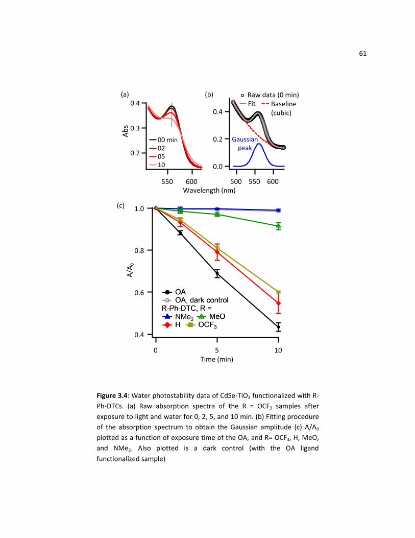
61
Figure 3.4: Water photostability data of CdSe-TiO2 functionalized with R-
Ph-DTCs. (a) Raw absorption spectra of the R = OCF3 samples after
exposure to light and water for 0, 2, 5, and 10 min. (b) Fitting procedure
of the absorption spectrum to obtain the Gaussian amplitude (c) A/A0
plotted as a function of exposure time of the OA, and R= OCF3, H, MeO,
and NMe2. Also plotted is a dark control (with the OA ligand
functionalized sample)
0.4
0.3
0.2
Ab
s
600550
00 min020510
1.0
0.8
0.6
0.4
A/A
0
1050Time (min)
(a) (b)
(c)
NMe2
Raw data (0 min)Fit
0.4
0.2
0.0
600550500Wavelength (nm)
Gaussian peak
Baseline (cubic)

62 of the ligands studied here. We found significant differences in QD photostability when we vary the
para-substituents of the R-Ph-DTC functionalized CdSe QD. Of these samples, the stability trend of the
samples of functionalized with R-Ph-DTCs is as follows: R = NMe2 > MeO > H ≈ OCF3. The increase in
electron donating ability of the R group was observed to increase the photostability of CdSe QDs. In the
time scale of this 10 min long photostability experiment, the photostability of the R = NMe2, most
electron donating substituent was remarkably within the error bars of the dark control.
3.3.3 Photoluminescence
We further investigated the mechanism of this increased stability. One explanation for this
stability is the hole transfers to the ligand molecule upon photoexcitation of the CdSe QD. Efficiency of
hole transfer can be measured with photoluminescence (PL) quenching experiments. This quenching has
been observed with CdSe QDs functionalized with thiols39-42 and dithiocarbamates;26,43 as photoexcited
holes are trapped in the ligand, the radiative recombination pathways of the QD decrease.44 To see
whether the photostability enhancement with electron-donating DTC ligands resulted from increased
hole transfer efficiency, we performed PL quenching experiments of CdSe QD suspended in chloroform
functionalized with R-Ph-DTCs, R = OCF3, H, MeO. For the PL experiments, we did not include the NMe2
substituent since the aniline starting reagent is visibly coloured and interfered with the PL signal from
the CdSe QDs. These experiments were done at an excitation wavelength of 450 nm. Results of these
experiments are shown in Figure 3.5. The PL spectrum of an OA-capped QD sample is also shown for
comparison. Overall, the DTC ligands quenched the PL as compared to the as-made (OA-capped) sample.
PL quenching efficiency trended as follows: R = OCF3 (amplitude of the PL peak is 63% of that of the OA)
< H (41% of OA) < MeO (1.4% of OA). To eliminate the effects of possible weakly bound anilines, we also
performed control experiments with exposure of QD suspensions to only the corresponding anilines (no
CS2 added), and they did not result in these significant changes in the PL signal. The PL trend suggests
that increasing the electron-donating ability of the DTC ligand results in the increased hole transfer
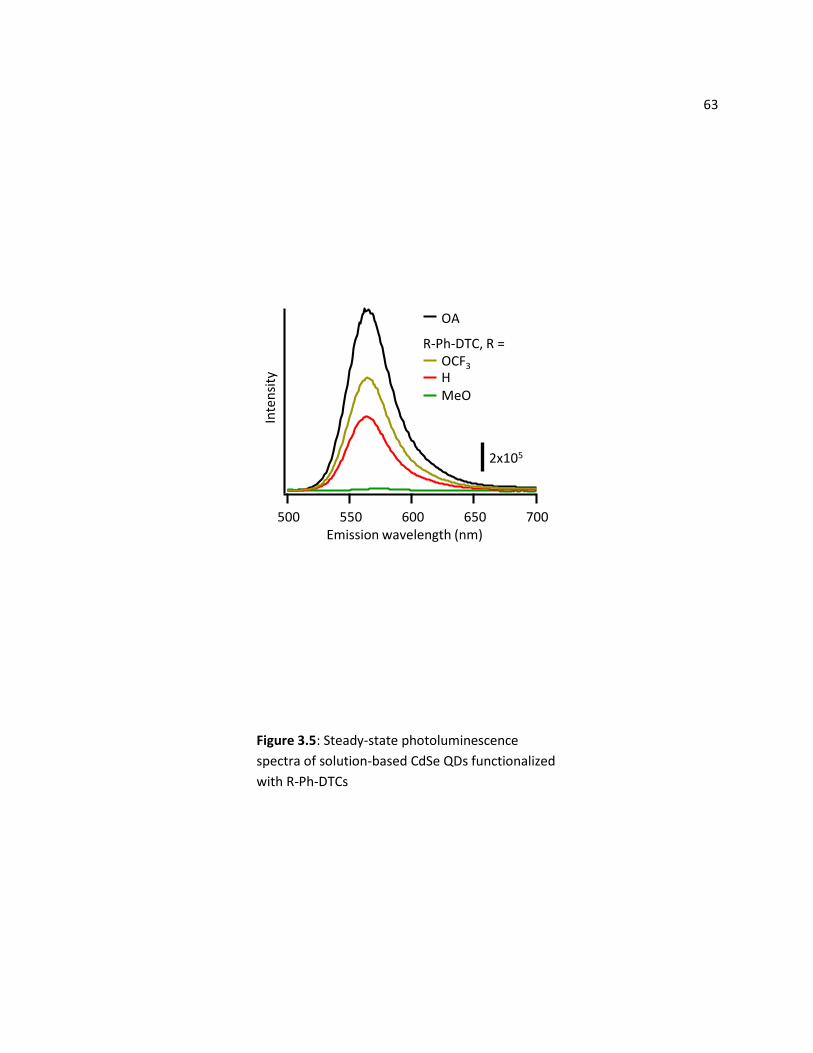
63
2x10⁵
Inte
nsi
ty
700650600550500Emission wavelength (nm)
OA
OCF3
HMeO
R-Ph-DTC, R =
Figure 3.5: Steady-state photoluminescence
spectra of solution-based CdSe QDs functionalized
with R-Ph-DTCs
64 efficiency from the QD into the ligand. The effective hole transfer into the ligand could explain the
photostability trend, in which holes are pulled away from the CdSe, thus protecting the QD core.
3.3.4 Photostability of DTC vs. Thiol Bound CdSe-TiO2 Surfaces
Increased stability also requires a strong and stable binding group. The most common binding
mode of the DTC group to transition metal ions is the bidentate configuration.37 Since the two sulfur
groups can bind to the CdSe surface in a bidentate fashion, DTCs can potentially bind more strongly than
thiols, the more commonly used head group used in QD ligand chemistry. Although the NMe2
substituent gave the best stability, this ligand also absorbs in the same region as the CdSe first exciton
peak and could interfere with comparative experiments with its corresponding thiol. Therefore, to make
the best comparison, we chose the thiol and DTC ligands with the MeO substituent. Both molecules lack
absorption features in the 475 – 600 nm region. Similar water photostability experiments were
performed as depicted and described in Figure 3.4, with exposures up to 20 min. Figure 3.6(a) shows the
A/A0 values over exposure time. The DTC functionalized CdSe was observed to be more stable than the
thiol. To investigate whether this effect simply resulted from molecular packing differences in the thiol
and DTC, XPS was performed. From XPS, we obtained 1.9 DTC molecules and 2.3 thiol molecules per nm2
of each ligand-QD surface. This shows that there were no significant differences in the molecular
packing; in fact we obtained more thiol than DTC molecules on the QD surface. We also investigated
rate of ligand loss over time with FTIR to determine whether the increased stability came from the
bidentate binding of the DTC head group. Experiments in the dark showed no significant changes in
ligand coverage when exposed to water for either ligand. Figure 3.6(b) shows the FTIR spectra of DTC or
thiol bound CdSe at 0 and 20 min of exposure to water in the dark. The characteristic features of the
surface-bound ligands remained the same, indicating no significant desorption of ligands in the
timescale of the experiment. Thus, the increased stability of DTC is not due to increased packing density
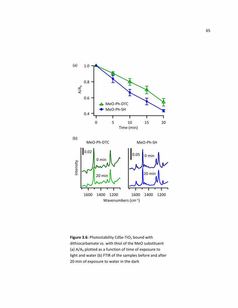
65
Figure 3.6: Photostability CdSe-TiO2 bound with
dithiocarbamate vs. with thiol of the MeO substituent
(a) A/A0 plotted as a function of time of exposure to
light and water (b) FTIR of the samples before and after
20 min of exposure to water in the dark
1.0
0.8
0.6
0.4
A/A
0
20151050Time (min)
MeO-Ph-DTC
MeO-Ph-SH
Wavenumbers (cm-1)
(a)
(b)MeO-Ph-DTC MeO-Ph-SH
0 min
20 min
0 min
20 min
0.02
1600 1400 1200
0.05
1600 1400 1200
Inte
nsi
ty
66 (which would restrict access to water and oxygen to the NP-ligand interface) or due to a stronger
binding to CdSe.
3.4 Discussion
Our experimental results show a few important pieces of information. First, we show that we
can functionalize DTCs on CdSe-TiO2 surfaces in-situ. However, in contrast to previous methods on gold,
in which a base was necessary to form the DTC, we found it preferable to omit the base for CdSe.
Second, the para-substituents on the DTC molecule have a large influence on the water photostability of
CdSe QDs, with electron-donating substituents providing higher stability. Finally, a comparison of thiol
and DTC binding groups yielded higher stability with the DTC group. Surprisingly however, this enhanced
stability is not due to differences in packing density or in the binding strengths of the functional groups.
We first address the role of the amine base on DTC functionalization to CdSe surfaces.
Although the synthesis of DTC molecules is traditionally done in the presence of base as the proton
acceptor,24,45 we found that the functionalization proceeded without it, and its presence even inhibited
the functionalization on CdSe. Amines can bind onto the surface of CdSe-TiO2, and consequently there
were some competitive binding of the TEA base onto our surfaces. Our work shows that while in-situ
functionalization of surfaces is convenient, we must also make sure that none of the individual starting
reagent readily binds to the surface and interfere with the grafting chemistry.
Next, we address the CdSe photostability functionalized with DTC vs. thiols. There have been
previous studies comparing stabilities of a bidentate sulfur ligand and the monodentate, with Au
surfaces (DTC vs. thiol head group) and solution-based CdSe QDs (carbodithiodate vs. thiol head group)
that found better stability with the bidentate ligands.23,46 However, the Au work is a thermal desorption
study in an ultrahigh vacuum XPS chamber.46 The carbodithiodate vs. thiol functionalized CdSe QDs work
was performed in non-aqueous solvents23 which may not accurately represent ligand-QD behaviour in
ambient air or water. In contrast, our studies were done in the presence of water and with a TiO2

67 electron acceptor. The aqueous instability of bidentate ligands was similarly found by Aldana et al.;21 in
fact, they found worse photostablity in the dithiol bound CdSe QDs than in the monothiol bound case,
due to ligand oxidation processes that takes place in aqueous conditions. Our work show that utilizing a
ligand head group that can chelate strongly to the QD may provide a stable ligand-QD adduct, but does
not necessarily give a more water- and photo-stable QD-TiO2 system, since the ligand themselves are
also susceptible to degradation from photogenerated charges in water and/or air. It is important to not
only have ligands that bind strongly, but also have hole-trapping electronic stabilization effects, as we
will discuss next.
Although we found no significant difference in ligand desorption of light exposed CdSe-DTC vs.
the CdSe-thiol QDs, the CdSe-DTC QDs were still more photostable. Studies on molecular junctions of
DTCs on Au46,47 and CdSe43 have found increased conductivity due to the resonant stabilization nature of
the NCS2 group resulting in a better π-conjugated system (as compared to a thiol). Similarly in our
system, the increased photostability in DTC functionalization could have also resulted from an enhanced
electronic effect from the DTC binding group. We further found that the CdSe-DTC photostability
depends on the para-substituent of phenyl DTCs. Previously, we showed enhanced QDs photostability
with electron-donating aromatic thiol ligands is due to the delocalization of the photogenerated holes
into the ligand molecule.19 Here we also observed this delocalization effect from the electron-donating
DTC groups. Our work suggests the importance of ligand electronic effects that could come from both
the ligand head group as well as the ligand molecular structure on the photostability of QDs.
Lastly, we note that the interpretation of the para substituent effects in our photostability
results is inconsistent with the work of Frederick et al.48 They investigated the para-substituent effect R-
Ph-DTCs on the electronic structure of CdSe QDs and counter-intuitively found that electron-
withdrawing ligands delocalized the holes more than the electron-donating. Ligand-CdSe behaviour is
known to be highly dependent on synthesis conditions and ligand passivation.49-52 Frederick et al.’s
68 experiments and DFT calculations were performed with amine passivated CdSe QDs. We did not use
amines in our system. Furthermore, our work focused on the water photostability of CdSe (with a TiO2
electron acceptor) and its relationship to the ligand molecular structure.
3.5 Conclusions
We have successfully functionalized conjugated dithiocarbamates on CdSe-TiO2 surfaces in-situ
to enable studies in factors that control ligand-QD photostability. When we compared the stability of
these conjugated DTCs to the corresponding thiols, we showed that the DTCs are more stable, but the
stability is not from the stronger binding of the DTC head group to the CdSe. The increased stability is
likely from an enhanced electronic effect of the DTC group. Furthermore, we found that the increased
electron donating ability of the substituent led to more stable QDs with a series of para-substituted
phenyl DTC ligands, and that this effect is from the favourable transfer and delocalization of the
photoexcited holes from the QD into the ligand.
3.6 References
1. Kamat, P. V. Quantum Dot Solar Cells. The Next Big Thing in Photovoltaics, J. Phys. Chem. Lett. 2013, 4, 908-918.
2. Colvin, V. L.; Schlamp, M. C.; Alivisatos, A. P. Light-Emitting-Diodes Made From Cadmium Selenide Nanocrystals And A Semiconducting Polymer, Nature 1994, 370, 354-357.
3. Konstantatos, G.; Howard, I.; Fischer, A.; Hoogland, S.; Clifford, J.; Klem, E.; Levina, L.; Sargent, E. H. Ultrasensitive Solution-Cast Quantum Dot Photodetectors, Nature 2006, 442, 180-183.
4. Shirasaki, Y.; Supran, G. J.; Bawendi, M. G.; Bulovic, V. Emergence of Colloidal Quantum-Dot Light-Emitting Technologies, Nat. Photonics 2013, 7, 13-23.
5. Katari, J. E. B.; Colvin, V. L.; Alivisatos, A. P. X-ray Photoelectron Spectroscopy of CdSe Nanocrystals with Applications to Studies of the Nanocrystal Surface, J. Phys. Chem. 1994, 98, 4109-4117.
6. Zidek, K.; Zheng, K.; Chabera, P.; Abdellah, M.; Pullerits, T. Quantum Dot Photodegradation Due to CdSe-ZnO Charge Transfer: Transient Absorption Study, Appl. Phys. Lett. 2012, 100.
7. Sykora, M.; Koposov, A. Y.; McGuire, J. A.; Schulze, R. K.; Tretiak, O.; Pietryga, J. M.; Klimov, V. I. Effect of Air Exposure on Surface Properties, Electronic Structure, and Carrier Relaxation in PbSe Nanocrystals, ACS Nano 2010, 4, 2021-2034.

69 8. Tvrdy, K.; Kamat, P. V. Substrate Driven Photochemistry of CdSe Quantum Dot Films: Charge
Injection and Irreversible Transformations on Oxide Surfaces, J. Phys. Chem. A 2009, 113, 3765-3772.
9. Barea, E. M.; Shalom, M.; Gimenez, S.; Hod, I.; Mora-Sero, I.; Zaban, A.; Bisquert, J. Design of Injection and Recombination in Quantum Dot Sensitized Solar Cells, J. Am. Chem. Soc. 2010, 132, 6834-6839.
10. Ihly, R.; Tolentino, J.; Liu, Y.; Gibbs, M.; Law, M. The Photothermal Stability of PbS Quantum Dot Solids, ACS Nano 2011, 5, 8175-8186.
11. Wang, Y. A.; Li, J. J.; Chen, H. Y.; Peng, X. G. Stabilization of Inorganic Nanocrystals by Organic Dendrons, J. Am. Chem. Soc. 2002, 124, 2293-2298.
12. Potapova, I.; Mruk, R.; Prehl, S.; Zentel, R.; Basche, T.; Mews, A. Semiconductor Nanocrystals with Multifunctional Polymer Ligands, J. Am. Chem. Soc. 2003, 125, 320-321.
13. Yildiz, I.; McCaughan, B.; Cruickshank, S. F.; Callan, J. F.; Raymo, F. M. Biocompatible CdSe-ZnS Core-Shell Quantum Dots Coated with Hydrophilic Polythiols, Langmuir 2009, 25, 7090-7096.
14. Fafarman, A. T.; Koh, W. K.; Diroll, B. T.; Kim, D. K.; Ko, D. K.; Oh, S. J.; Ye, X. C.; Doan-Nguyen, V.; Crump, M. R.; Reifsnyder, D. C.; et. al. Thiocyanate-Capped Nanocrystal Colloids: Vibrational Reporter of Surface Chemistry and Solution-Based Route to Enhanced Coupling in Nanocrystal Solids, J. Am. Chem. Soc. 2011, 133, 15753-15761.
15. Law, M.; Luther, J. M.; Song, O.; Hughes, B. K.; Perkins, C. L.; Nozik, A. J. Structural, Optical, and Electrical Properties of PbSe Nanocrystal Solids Treated Thermally or with Simple Amines, J. Am. Chem. Soc. 2008, 130, 5974-5985.
16. Foos, E. E. The Complex Interaction of Spectroscopic Shifts and Electronic Properties in Semiconductor Nanocrystal Films, J. Phys. Chem. Lett. 2013, 4, 625-632.
17. Frederick, M. T.; Amin, V. A.; Cass, L. C.; Weiss, E. A. A Molecule to Detect and Perturb the Confinement of Charge Carriers in Quantum Dots, Nano Lett. 2011, 11, 5455-5460.
18. Liang, Y.; Thorne, J. E.; Parkinson, B. A. Controlling the Electronic Coupling between CdSe Quantum Dots and Thiol Capping Ligands via pH and Ligand Selection, Langmuir 2012.
19. Tan, Y.; Jin, S.; Hamers, R. J. Influence of Hole-Sequestering Ligands on the Photostability of CdSe Quantum Dots, J. Phys. Chem. C 2013, 117, 313-320.
20. Schapotschnikow, P.; Hommersom, B.; Vlugt, T. J. H. Adsorption and Binding of Ligands to CdSe Nanocrystals, J. Phys. Chem. C 2009, 113, 12690-12698.
21. Aldana, J.; Wang, Y. A.; Peng, X. G. Photochemical Instability of CdSe Nanocrystals Coated by Hydrophilic Thiols, J. Am. Chem. Soc. 2001, 123, 8844-8850.
70 22. Parak, W. J.; Gerion, D.; Pellegrino, T.; Zanchet, D.; Micheel, C.; Williams, S. C.; Boudreau, R.; Le
Gros, M. A.; Larabell, C. A.; Alivisatos, A. P. Biological Applications of Colloidal Nanocrystals, Nanotechnology 2003, 14, R15-R27.
23. Querner, C.; Reiss, P.; Bleuse, J.; Pron, A. Chelating Ligands for Nanocrystals' Surface Functionalization, J. Am. Chem. Soc. 2004, 126, 11574-11582.
24. Coucouvanis, D. Chemistry of the Dithioacid and 1,1-Dithiolate Complexes, Prog. Inorg. Chem. 1970, 11, 233-371.
25. Algar, W. R.; Krull, U. J. Luminescence and Stability of Aqueous Thioalkyl Acid capped CdSe/ZnS Quantum Dots Correlated to Ligand Ionization, Chemphyschem 2007, 8, 561-568.
26. Dubois, F.; Mahler, B.; Dubertret, B.; Doris, E.; Mioskowski, C. A Versatile Strategy for Quantum Dot Ligand Exchange, J. Am. Chem. Soc. 2007, 129, 482-483.
27. Wang, J.; Xu, J.; Goodman, M. D.; Chen, Y.; Cai, M.; Shinar, J.; Lin, Z. A Simple Biphasic Route to Water Soluble Dithiocarbamate Functionalized Quantum Dots, J. Mater. Chem. 2008, 18, 3270-3274.
28. Zhu, H.; Coleman, D. M.; Dehen, C. J.; Geisler, I. M.; Zemlyanov, D.; Chmielewski, J.; Simpson, G. J.; Wei, A. Assembly of Dithiocarbamate-Anchored Monolayers on Gold Surfaces in Aqueous Solutions, Langmuir 2008, 24, 8660-8666.
29. Zhao, Y.; Perez-Segarra, W.; Shi, Q. C.; Wei, A. Dithiocarbamate Assembly on Gold, J. Am. Chem. Soc. 2005, 127, 7328-7329.
30. Ito, S.; Murakami, T. N.; Comte, P.; Liska, P.; Gratzel, C.; Nazeeruddin, M. K.; Gratzel, M. Fabrication of Thin Film Dye Sensitized Solar Cells with Solar to Electric Power Conversion Efficiency Over 10%, Thin Solid Films 2008, 516, 4613-4619.
31. Peng, Z. A.; Peng, X. G. Formation of High-Quality CdTe, CdSe, and CdS Nanocrystals using CdO as Precursor, J. Am. Chem. Soc. 2001, 123, 183-184.
32. Yu, W. W.; Qu, L. H.; Guo, W. Z.; Peng, X. G. Experimental Determination of the Extinction Coefficient of CdTe, CdSe, and CdS Nanocrystals, Chem. Mater. 2003, 15, 2854-2860.
33. Guijarro, N.; Lana-Villarreal, T.; Mora-Sero, I.; Bisquert, J.; Gomez, R. CdSe Quantum Dot-Sensitized TiO2 Electrodes: Effect of Quantum Dot Coverage and Mode of Attachment, J. Phys. Chem. C 2009, 113, 4208-4214.
34. Selinsky, R. S.; Ding, Q.; Faber, M. S.; Wright, J. C.; Jin, S. Quantum Dot Nanoscale Heterostructures for Solar Energy Conversion, Chem. Soc. Rev. 2013, 42, 2963-2985.
35. Pernik, D. R.; Tvrdy, K.; Radich, J. G.; Kamat, P. V. Tracking the Adsorption and Electron Injection Rates of CdSe Quantum Dots on TiO2: Linked versus Direct Attachment, J. Phys. Chem. C 2011, 115, 13511-13519.
71 36. Young, A. G.; Al-Salim, N.; Green, D. P.; McQuillan, A. J. Attenuated Total Reflection Infrared
Studies of Oleate and Trioctylphosphine Oxide Ligand Adsorption and Exchange Reactions on CdS Quantum Dot Films, Langmuir 2008, 24, 3841-3849.
37. Hogarth, G. Transition Metal Dithiocarbamates: 1978 - 2003, Prog. Inorg. Chem. 2005, 53, 71-563.
38. Norris, D. J.; Bawendi, M. G. Measurement and Assignment of the Size-Dependent Optical Spectrum in CdSe Quantum Dots, Phys. Rev. B 1996, 53, 16338-16346.
39. Koole, R.; Schapotschnikow, P.; Donega, C. d. M.; Vlugt, T. J. H.; Meijerink, A. Time-Dependent Photoluminescence Spectroscopy as a Tool to Measure the Ligand Exchange Kinetics on a Quantum Dot Surface, ACS Nano 2008, 2, 1703-1714.
40. Liu, I. S.; Lo, H.-H.; Chien, C.-T.; Lin, Y.-Y.; Chen, C.-W.; Chen, Y.-F.; Su, W.-F.; Liou, S.-C. Enhancing Photoluminescence Quenching and Photoelectric Properties of CdSe Quantum Dots with Hole Accepting Ligands, J. Mater. Chem. 2008, 18, 675-682.
41. Munro, A. M.; Jen-La Plante, I.; Ng, M. S.; Ginger, D. S. Quantitative Study of the Effects of Surface Ligand Concentration on CdSe Nanocrystal Photoluminescence, J. Phys. Chem. C 2007, 111, 6220-6227.
42. Wuister, S. F.; Donega, C. D.; Meijerink, A. Influence of Thiol Capping on the Exciton Luminescence and Decay Kinetics of CdTe and CdSe Quantum Dots, J. Phys. Chem. B 2004, 108, 17393-17397.
43. Zotti, G.; Vercelli, B.; Berlin, A.; Virgili, T. Multi layers of CdSe Nanocrystals and Bis(dithiocarbamate) Linkers Displaying Record Photoconduction, J. Phys. Chem. C 2012, 116, 25689-25693.
44. Ning, Z.; Molnar, M.; Chen, Y.; Friberg, P.; Gan, L.; Agren, H.; Fu, Y. Role of Surface Ligands in Optical Properties of Colloidal CdSe/CdS Quantum Dots, Phys. Chem. Chem. Phys. 2011, 13, 5848-5854.
45. Ewing, S. P.; Lockshon, D.; Jencks, W. P. Mechanism of Cleavage of Carbamate Anions, J. Am. Chem. Soc. 1980, 102, 3072-3084.
46. von Wrochem, F.; Gao, D.; Scholz, F.; Nothofer, H.-G.; Nelles, G.; Wessels, J. M. Efficient Electronic Coupling and Improved Stability with Dithiocarbamate-Based Molecular Junctions, Nature Nanotechnol. 2010, 5, 618-624.
47. Wessels, J. M.; Nothofer, H. G.; Ford, W. E.; von Wrochem, F.; Scholz, F.; Vossmeyer, T.; Schroedter, A.; Weller, H.; Yasuda, A. Optical and Electrical Properties of Three-Dimensional Interlinked Gold Nanoparticle Assemblies, J. Am. Chem. Soc. 2004, 126, 3349-3356.
48. Frederick, M. T.; Amin, V. A.; Swenson, N. K.; Ho, A. Y.; Weiss, E. A. Control of Exciton Confinement in Quantum Dot-Organic Complexes through Energetic Alignment of Interfacial Orbitals, Nano Lett. 2013, 13, 287-292.
72 49. Bullen, C.; Mulvaney, P. The Effects of Chemisorption on the Luminescence of CdSe Quantum
Dots, Langmuir 2006, 22, 3007-3013.
50. Green, M. The nature of quantum dot capping ligands, J. Mater. Chem. 2010, 20, 5797-5809.
51. Guyot-Sionnest, P.; Wehrenberg, B.; Yu, D. Intraband relaxation in CdSe nanocrystals and the strong influence of the surface ligands, J. Chem. Phys. 2005, 123.
52. Talapin, D. V.; Rogach, A. L.; Kornowski, A.; Haase, M.; Weller, H. Highly luminescent monodisperse CdSe and CdSe/ZnS nanocrystals synthesized in a hexadecylamine-trioctylphosphine oxide-trioctylphospine mixture, Nano Lett. 2001, 1, 207-211.
73
Chapter 4
Spectroelectrochemistry of the Iodide-Triiodide Redox Couple
4.1 Introduction
Dye sensitized solar cells (DSSCs) offer a low cost alternative to the more expensive
conventional single crystalline silicon p-n junction cells.1 In this liquid junction solar cell, a dye absorbs
sunlight and transfers electrons into a mesoporous TiO2 nanocrystalline film. A redox shuttle then
replenishes the electrons and a counter electrode (CE) completes the cell. The standard electrolyte
material for the redox shuttle is the iodide-triiodide couple and the standard CE material is platinized
transparent conducting glass. There have been efforts to replace the iodine based electrolytes, most
promisingly with cobalt complexes,2,3 but most do not perform as well as the iodine-based ones. The
iodide-triiodide redox couple yielded the best performing cells because the large difference in oxidation-
reduction kinetics reduces electron recombination rates. On the dye-TiO2 side, oxidation kinetics from
the iodide to triiodide is much faster than the reverse reaction, thus reducing electron recombination
from the dye or the TiO2 back to the redox electrolyte.4
On the CE side however, a fast reduction of triiodide is desirable to regenerate the iodide
species. Pt has been the classical CE material due to its high stability in the iodine electrolyte and
catalytic properties of triiodide reduction.5 Alternatives to the rare and expensive Pt have been
explored, among them conductive organic polymers,6-8 carbon materials,9,10 inorganic materials such as
metal sulfides,11,12 metal oxides,13,14 metal carbides,15 and metal nitrides.15,16 While the mechanism of
triiodide reduction is well-studied on Pt,5,17 the mechanism has not been fully understood for these Pt-
free CEs. One can speculate a similar mechanism as on the Pt; a rational screening method has been
done recently through density functional theory calculations. This work explored a large series of metals
and inorganic semiconductors.13 Studies of carbon materials and conducting polymers have largely

74 focused on optimizing the electrode physical micro-structure, not on the fundamental mechanism of
catalysis.7,9 A better understanding of the iodine redox chemistry on these organic materials is important
for the design of inexpensive, effective CE materials.
Spectroelectrochemistry is a useful tool that allows us to monitor changes in the concentrations
of the redox species if there are signature differences in their absorption behaviour. Since the iodine
species used in DSSCs have differentiable UV-visible absorption spectra, we could use this technique to
compare electrochemical behaviour of different electrodes. This chapter discusses the use of in-situ UV-
visible spectroscopy to identify electrogenerated iodine species and monitor their concentrations
changes as function of electric potential. We will first explore changes at a platinum electrode, then
extend it to one of the conducting polymers used as an alternative CE in DSSC, poly(3,4-
ethylenedioxythiophene) poly(styrenesulfonate) or PEDOT-PSS.
4.2 Mechanism of Electrochemical Reactions of the Iodide-Triiodide Redox Couple on Platinum
The electrochemistry of iodine involves multiple species. Starting from iodide (I-), it can be
oxidized to triiodide (I3-), and then be further oxidized to iodine (I2):
(A) 3I- ↔ I3- + 2e-
(B) 2I3- ↔ 3I2 + 2e-
Furthermore, the concentrations of these three polyiiodide species are in equilibrium with each other, I-
+ I2 I3-, with the equilibrium highly shifted toward the formation of triiodide (Keq = 107 at 25 C).5 On
Pt, the reaction mechanism is as follows:
(1) I3- (sol) I2(sol) + I- (sol)
(2) I2 (sol) + e- + S I- + I(ads)
(3) I (ads) + e- I- (sol)
75 S represents an active site on the electrode surface. The (sol) indicates the species is in solution while
(ads) indicates the species is adsorbed on the surface. The rate determining step of this reduction is
reaction (2), in which the iodine adsorbs to an active site of the Pt and produces an iodide ion.5,17
4.3 Experimental
4.3.1 Materials
Lithium iodide (anhydrous, 99%, Acros Organics), Iodine (≥99.8%, Columbus Chemical Industries,
Inc.), Lithium perchlorate (99.99%, Aldrich), and Poly(3,4-ethylenedioxythiophene)-
poly(styrenesulfonate), 1.3 wt% dispersion in H2O (Aldrich) were used as received. Fluorine-doped tin
oxide (FTO) coated glass (Hartford Glass) was cleaned with detergent, then rinsed with acetone and
ethanol before use. Platinum foil (0.127 mm thick, 99.9% metal basis, Alfa Aesar) and platinum wire
(0.25 mm diameter, 99.99%, Aldrich) were cleaned by soaking in concentrated H2SO4 overnight. They
were rinsed thoroughly with deionized H2O, and dried immediately prior to use. For the PEDOT-PSS
electrodes, the polymer solution was spin-coated on FTO glass at 5000 rpm for 1 min, and dried at 110
C for 5 min. The thickness of the polymer film was 70 nm as measured by ellipsometry.
4.3.2 Electrochemistry
Cyclic voltammetry was performed with a Gamry potentiostat (Series G 300) with a Pt wire as
the counter electrode and another Pt wire as the reference electrode. The Ag/AgCl and the Ag/Ag+ are
commonly used reference electrodes, but we had long term problems from the formation of AgI
precipitating out and clogging the Vycor frit. Therefore, we resorted to using Pt wire as a pseudo-
reference electrode. All cyclic voltammograms shown here were performed with 3 mM LiI, 0.5 M LiClO4
in acetonitrile (ACN) at a scan rate of 25 mV/s, starting at the open circuit potential. LiClO4 was added as
a supporting electrolyte and did not have any redox activity in the potential window explored here.
76 4.3.3 Spectroelectrochemistry
Experiments were performed using a home-built cell in specular reflection mode. A detailed
technical design and drawing of the cell is shown in the Appendix A2 section of this thesis. A fused silica
window was fitted onto the top of the cell to allow light penetration. The cell was made leak-proof by
sealing the multiple components with properly positioned Kalrez O-rings. Contact from the electrodes to
the potentiostat clips was made through Cu tape. Electrolyte solution was flowed through the cell at a
constant rate of 0.6 mL/min with a syringe pump. A fiber optic cable bundle, angled normal to the
working electrode surface, served to deliver and collect the reflected light. UV-visible light was sourced
from a Mickropack (DH-2000) unit, equipped with deuterium (UV) and tungsten (visible-NIR) lamps, and
the subsequent reflected light was fed into an Ocean Optics spectrometer (USB-2000). Raw intensity
scans were taken every 2 s, at voltage steps of 50 mV. A reference scan (I0) was taken at open circuit
potential (0 mV) and the absorbance was then calculated using A = -log(I/I0).
4.4 Results and Discussion
4.4.1 Absorption Spectra of Iodine Species
The absorption spectra of the three different iodine species in acetonitrile (ACN) are shown in
Figure 4.1(a), taken in specular reflection mode with Pt as the substrate. To make the triiodide ions, we
mixed equal concentrations of LiI and I2. The equilibrium constant of I- + I2 I3- is markedly shifted to
the right,5 so almost all of the iodine species should exist as triiodide ions. Iodide ions exhibit absorption
only in the deeper UV region (220 – 275 nm), while the triiodide ions have three distinct peaks at 243,
291, and 362 nm, with the last peak extending into the visible. The absorption of molecular iodine in
ACN is mainly in the visible, with a peak at 460 nm, and two smaller peaks at 291 and 362 nm. These
spectra were not taken at the same concentrations; we had to dilute the triiodide solution > 25x to put
all of them at the same scale because the triiodide ions absorbs much more strongly than the iodine.
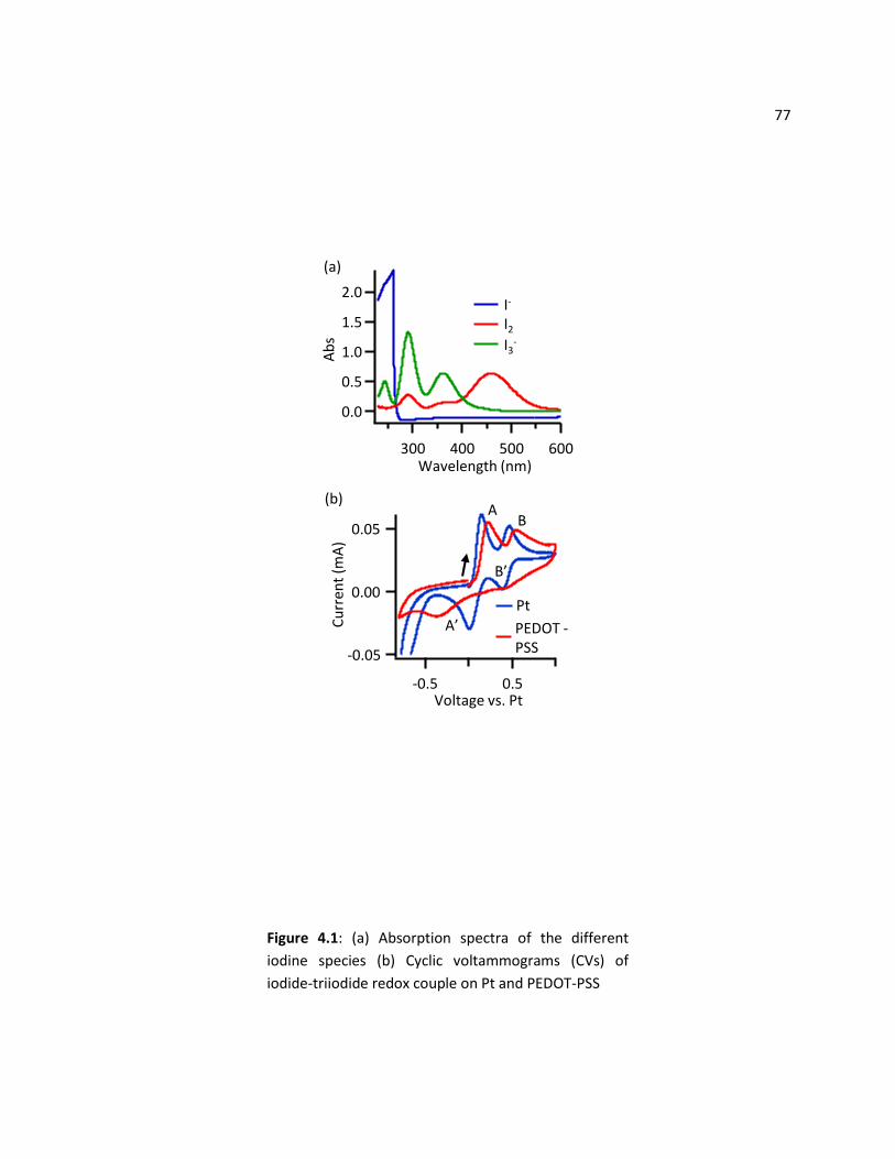
77
Figure 4.1: (a) Absorption spectra of the different
iodine species (b) Cyclic voltammograms (CVs) of
iodide-triiodide redox couple on Pt and PEDOT-PSS
2.0
1.5
1.0
0.5
0.0
Ab
s
600500400300Wavelength (nm)
I-
I2
I3-
(a)
(b)
0.05
0.00
-0.05
Cu
rren
t (m
A)
-0.5 0.5Voltage vs. Pt
PEDOT -PSS
Pt
A
A’
B’
B
78 The absorption coefficients (in units of L/mol-cm) are 24091 at 363 nm and 44881 at 293 nm for I3
-, but
only 837 at 463nm for I2.18
4.4.2 Electrochemistry of the Iodide-Triiodide Couple on Pt and PEDOT-PSS
Figure 4.1(b) shows cyclic voltammograms of 3 mM LiI, 0.5 M LiClO4 in ACN on Pt or PEDOT-PSS
electrodes at a scan rate of 25 mV/s. Starting at the open circuit potential (0 mV vs. Pt), the cell was
cycled toward more oxidizing potential first, and then reversed. For both Pt and PEDOT-PSS samples, we
observed two oxidization and two reduction peaks. As discussed previously, these peaks corresponded
to the oxidation of iodide to triiodide (reaction A), subsequently another oxidation from triiodide to
iodine (reaction B), and their respective reduction reactions when the potentials were reversed. For Pt,
the peak to peak splittings for the respective processes are:
(A) ∆EA = Ep,a(A) – Ep,c(A’) 149 – 13 = 136 mV
(B) ∆EB = Ep,a(B) – Ep,c(B’) 465 – 393 = 72 mV
These values indicate that reaction A is more sluggish than reaction B, as observed by others, and the
slow reaction of process A was attributed to a non-electroactive layer of iodine absorbed onto the
surface of Pt, impeding the reduction of triiodide.18,19
The iodide-triiodide oxidation-reduction behaviour was more sluggish on PEDOT-PSS than on Pt,
as observed by larger overpotentials and peak to peak splittings. For this electrode, the ∆EA = 572 mV
and ∆EB = 93 mV. Another striking difference on this electrode is the very broad reduction peaks for both
processes. Peak widths could indicate the reversibility of a reaction, and a broader peak indicates a less
reversible reaction.20 The large discrepancy of oxidation and reduction kinetics on this polymer could be
explained by the adsorption of non-electroactive iodine species in the film, blocking electron transfer.
Molecular iodine is known to form charge transfer complexes with conjugated organic molecules,21 and
a few previous studies have shown that these complexes form with thiophene22 and PEDOT.23 Once
79 iodine is formed, it can then be trapped in the microstructure of the polymer film through the formation
of these complexes, as shown by X-ray photoelectron spectroscopy studies.24
4.4.3 Spectroelectrochemistry
Figure 4.2 shows the results from spectroelectrochemistry experiments on Pt electrode. The
cyclic voltammogram is shown on Figure 4.2(a). To show changes in the spectral behaviour, the
voltammogram is divided into three regions. Representative spectra are shown in Figures (b), (c), and (d)
corresponding to regions 1, 2, and 3 respectively. Region 1 is the oxidation of iodide to triiodide and
subsequently from triiodide to iodine. In the absorbance spectra of this region, we detected an increase
in the concentration of triiodide as expected at potentials of the first oxidation peak (reaction A).
However, we did not detect the presence of molecular iodine as a separate peak at potentials of the
second oxidation peak (reaction B). Iodine was probably produced, but triiodide also absorbs in the
same region and both species have similar absorption coefficients at 462 nm (ε 837 L/mol-cm for
iodine, ε 1053 for triiodide).18 Furthermore, since iodide is in excess in the bulk solution, any iodine
that was produced would be quickly converted into triiodide. Sweeping back reduces the iodine to
triiodide (reaction B’, region 2). In this region, we observed the further increase of triiodide
concentration. At the reducing potential of region 3, the triiodide ions are reduced back to iodide ions.
The absorption spectra in this region confirmed this reaction, and showed a decreasing trend in the
triiodide concentration. We were able to map out the trends in triiodide concentrations with potential
cycling that corresponded to the oxidation-reduction reactions in the cell.
Figure 4.3 shows results from a similar spectroelectrochemistry experiment performed on the
PEDOT-PSS electrode. The cyclic voltammogram is shown in Figure 4.3(a). In Figure 4.3(b), we also
included the reference spectra of the three iodine species, taken from specular reflectance of the
PEDOT-PSS film on FTO glass. Due to differences in substrates, these spectra were observed to be
slightly different from those observed in the Pt case in Figure 4.1(a). However, general features were

80
Figure 4.2: (a) CV of iodide-triiodide redox couple on Pt (b)-(d)
Absorption spectra corresponding to regions (b) 1, (c) 2, and (d)
3 from the CV scan
0.08
0.06
0.04
0.02
0.00
Ab
s
500400300Wavelength (nm)
800 mV600400
0.2
0.1
0.0
-0.1
Cu
rren
t (m
A)
-0.2 0.2 0.6
Voltage vs. Pt
on Pt, 25mV/s
1
2
3
0.04
0.02
0.00A
bs
500400300
Wavelength (nm)
100 mV300500700
0.06
0.04
0.02
0.00
Ab
s
500400300Wavelength (nm)
100 mV-100-300
1
2 3
(a) (b)
(c) (d)
81 qualitatively similar. With this electrode, the spectroelectrochemistry experiment had an extra
complication from the electrochromic behaviour of PEDOT-PSS. The polymer film as spincoated
exhibited a light blue colour. At oxidizing potentials, the polymer becomes more doped and less
coloured in the visible. At reducing potentials, dedoping of the polymer occurs, and it becomes more
coloured.25 Absorption spectra from two marked regions are shown in subfigures 4.3(c) and 4.3(d). To
spectrally differentiate the iodide electrochemistry from the film electrochromism, we also performed a
background experiment with an electrolyte solution without any LiI. We included representative spectra
from this experiment in figures 4.3(c) and 4.3(d).
The changes in the electrolyte species on the PEDOT-PSS film were observed to be similar to the
Pt. The triiodide concentration increased at oxidizing potentials as shown in Figure 4.3(c), and decreased
at reducing potentials as in Figure 4.3(d) corresponding to the peaks from the cyclic voltammogram.
Again, we did not detect any iodine formation at the proper potentials. Comparing the spectral
experiments with and without the iodide ions revealed changes in the polymer film when exposed to
the iodide electrochemistry. Absorbance changes are more striking in the iodide solution especially in
the 500 – 750 nm region; the film lost more colour when oxidized and became more coloured when
reduced as compared to the background. This region did not correspond to native absorption signatures
of any iodine species and could be attributed to physical changes in film. The original counterion for the
film is PSS, but it could be swapped out after electrochemical cycling to other negatively charged ions in
the solution (iodide, triiodide, or perchlorate). Changes in polymer counterion are known to affect the
spectroelectrochemical behaviour of the film.26 Another explanation could be formation of charge
transfer complexes of PEDOT chains to iodine species. The charge transfer complex between iodine and
thiophene was found to have absorption peaks at 299 and 368 nm.22 If PEDOT-iodine complex has
similar absorption bands, it would be difficult to differentiate due to overlaps with the triiodide
absorption. However, it is more likely that the absorption bands are shifted, since PEDOT is different
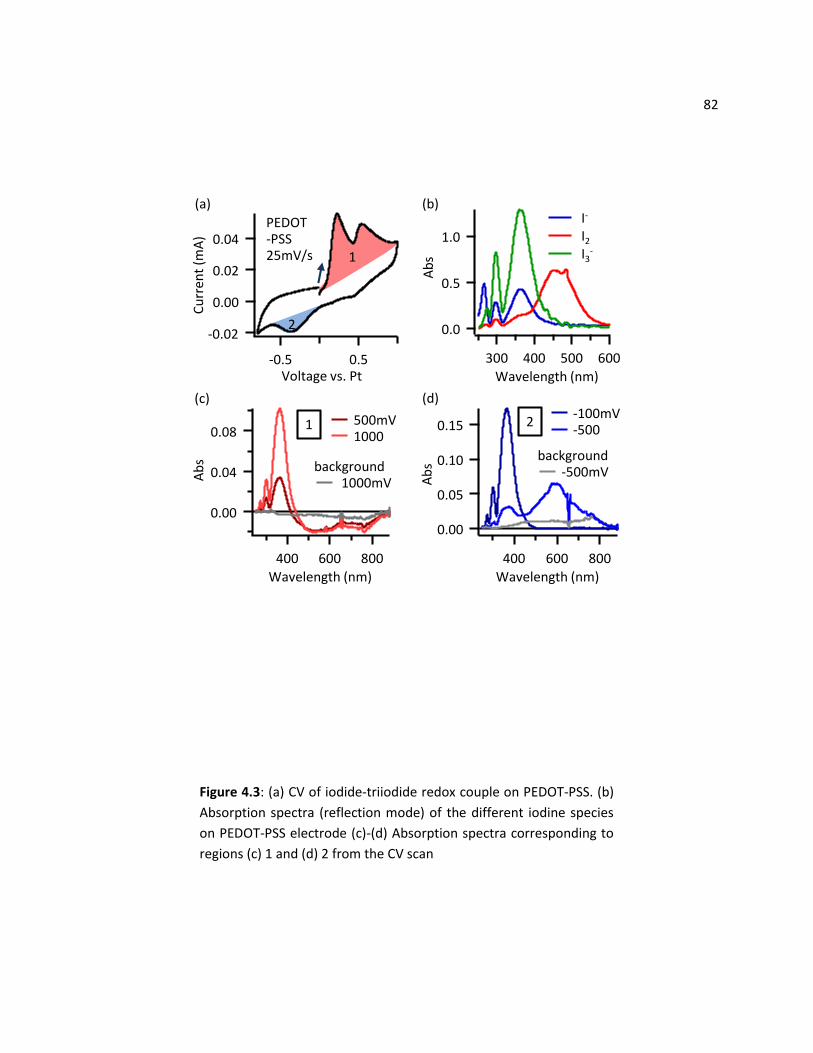
82
Figure 4.3: (a) CV of iodide-triiodide redox couple on PEDOT-PSS. (b)
Absorption spectra (reflection mode) of the different iodine species
on PEDOT-PSS electrode (c)-(d) Absorption spectra corresponding to
regions (c) 1 and (d) 2 from the CV scan
1.0
0.5
0.0
Ab
s
600500400300
Wavelength (nm)
I-
I2
I3-
0.08
0.04
0.00
Ab
s
800600400
Wavelength (nm)
500mV1000
background1000mV
0.15
0.10
0.05
0.00
Ab
s
800600400
Wavelength (nm)
-100mV-500
background-500mV
0.04
0.02
0.00
-0.02
Cu
rren
t (m
A)
-0.5 0.5Voltage vs. Pt
PEDOT-PSS25mV/s 1
2
1 2
(a) (b)
(c) (d)
83 from the parent monomer thiophene with its delocalization of charges throughout the polymer chain.
More studies are needed to understand the changes in the PEDOT-PSS after electrochemical cycling to
explain these spectral differences in the films.
4.5 Conclusions
Understanding the behaviour of iodide-triiodide electrochemistry on Pt-free counter electrodes
for DSSCs is important for the design of better performing cheaper catalyst materials for triiodide
reduction. Spectroelectrochemistry is a potentially useful tool for this study, since there are spectral
differences in the various polyiodide species. We show that we can successfully monitor spectral
changes in the triiodide concentrations with cyclic voltammetry for both Pt and PEDOT-PSS (an
alternative CE material) electrodes. On PEDOT-PSS, the spectral changes in the visible region were found
to be due to the electrochromic behaviour of the polymer film; this can mask the detection of any iodine
species in that absorb in the visible. Complementary experiments are needed to monitor physical
changes in the PEDOT-PSS films with electrochemical cycling of polyiodine electrolytes.
4.6 References
1. Oregan, B.; Grätzel, M. A Low-Cost, High-Efficiency Solar-Cell Based on Dye-Sensitized Colloidial TiO2 Films, Nature 1991, 353, 737-740.
2. Feldt, S. M.; Gibson, E. A.; Gabrielsson, E.; Sun, L.; Boschloo, G.; Hagfeldt, A. Design of Organic Dyes and Cobalt Polypyridine Redox Mediators for High-Efficiency Dye-Sensitized Solar Cells, J. Am. Chem. Soc. 2010, 132, 16714-16724.
3. Yella, A.; Lee, H. W.; Tsao, H. N.; Yi, C. Y.; Chandiran, A. K.; Nazeeruddin, M. K.; Diau, E. W. G.; Yeh, C. Y.; Zakeeruddin, S. M.; Gratzel, M. Porphyrin-Sensitized Solar Cells with Cobalt (II/III)-Based Redox Electrolyte Exceed 12 Percent Efficiency, Science 2011, 334, 629-634.
4. Gregg, B. A.; Pichot, F.; Ferrere, S.; Fields, C. L. Interfacial Recombination Processes in Dye-Sensitized Solar Cells and Methods to Passivate the Interfaces, J. Phys. Chem. B 2001, 105, 1422-1429.
5. Macagno, V. A.; Giordano, M. C.; Arvia, A. J. Kinetics and Mechanisms of Electrochemical Reaction on Platinum with Solutions of Iodine-Sodium Iodide in Acetonitrile, Electrochim. Acta 1969, 14, 335-357.
84 6. Li, Q.; Wu, J.; Tang, Q.; Lan, Z.; Li, P.; Lin, J.; Fan, L. Application of Microporous Polyaniline
Counter Electrode for Dye-Sensitized Solar Cells, Electrochem. Commun. 2008, 10, 1299-1302.
7. Saito, Y.; Kubo, W.; Kitamura, T.; Wada, Y.; Yanagida, S. I-/I-3(-) Redox Reaction Behavior on Poly(3,4-ethylenedioxythiophene) Counter Electrode in Dye-Sensitized Solar Cells, J. Photochem. Photobiol. A 2004, 164, 153-157.
8. Ahmad, S.; Yum, J.-H.; Zhang, X.; Grätzel, M.; Butt, H.-J.; Nazeeruddin, M. K. Dye-Sensitized Solar Cells Based on Poly (3,4-ethylenedioxythiophene) Counter Electrode Derived from Ionic Liquids, J. Mater. Chem. 2010, 20, 1654-1658.
9. Murakami, T. N.; Graetzel, M. Counter Electrodes for DSC: Application of Functional Materials as Catalysts, Inorg. Chim. Acta 2008, 361, 572-580.
10. Trancik, J. E.; Barton, S. C.; Hone, J. Transparent and Catalytic Carbon Nanotube Films, Nano Lett. 2008, 8, 982-987.
11. Wang, M.; Anghel, A. M.; Marsan, B.; Ha, N.-L. C.; Pootrakulchote, N.; Zakeeruddin, S. M.; Graetzel, M. CoS Supersedes Pt as Efficient Electrocatalyst for Triiodide Reduction in Dye-Sensitized Solar Cells, J. Am. Chem. Soc. 2009, 131, 15976-15977.
12. Sun, H.; Qin, D.; Huang, S.; Guo, X.; Li, D.; Luo, Y.; Meng, Q. Dye-Sensitized Solar Cells with NiS Counter Electrodes Electrodeposited by a Potential Reversal Technique, Energy Environ. Sci. 2011, 4, 2630-2637.
13. Hou, Y.; Wang, D.; Yang, X. H.; Fang, W. Q.; Zhang, B.; Wang, H. F.; Lu, G. Z.; Hu, P.; Zhao, H. J.; Yang, H. G. Rational Screening Low-Cost Counter Electrodes for Dye-Sensitized Solar Cells, Nat. Commun. 2013, 4, 1583-1583.
14. Wu, M.; Lin, X.; Hagfeldt, A.; Ma, T. A Novel Catalyst of WO2 Nanorod for the Counter Electrode of Dye-Sensitized Solar Cells, Chem. Comm. 2011, 47, 4535-4537.
15. Wu, M.; Lin, X.; Wang, Y.; Wang, L.; Guo, W.; Qu, D.; Peng, X.; Hagfeldt, A.; Graetzel, M.; Ma, T. Economical Pt-Free Catalysts for Counter Electrodes of Dye-Sensitized Solar Cells, J. Am. Chem. Soc. 2012, 134, 3419-3428.
16. Li, G.-R.; Wang, F.; Jiang, Q.-W.; Gao, X.-P.; Shen, P.-W. Carbon Nanotubes with Titanium Nitride as a Low-Cost Counter-Electrode Material for Dye-Sensitized Solar Cells, Angew. Chem. Int. Ed. 2010, 49, 3653-3656.
17. Dane, L. M.; Janssen, L. J. J.; Hoogland, J. G. The Iodine/ Iodide Redox Couple at a Platinum Electrode, Electrochim. Acta 1968, 13, 507-518.
18. Hanson, K. J.; Matlosz, M. J.; Tobias, C. W.; Newman, J. Electrochemistry of Iodide in Propylene Carbonate .2. Theoretical-Model, J. Electrochem. Soc. 1987, 134, 2210-2215.
19. Hubbard, A. T.; Osteryou.Ra; Anson, F. C. Further Studies of Iodide-Iodine Couple at Platinum Electrodes by Thin Layer Electrochemistry, Anal. Chem. 1966, 38, 692-697.

85 20. Bard, A. J.; Faulkner, L. R. Electrochemical Methods: Fundamentals and Applications, 2nd ed.;
Wiley, 2000.
21. Benesi, H. A.; Hildebrand, J. H. A Spectrometric Investigation of the Interaction of Iodine with Aromatic Hydrocarbons J. Am. Chem. Soc. 1949, 71, 2703-2707.
22. Ulagendran, V.; Kumar, R.; Jayakumar, S.; Kannappan, V. Ultrasonic and Spectroscopic Investigations of Charge-Transfer Complexes in Ternary Liquid Mixtures, J. Mol. Liq. 2009, 148, 67-72.
23. Biallozor, S.; Kupniewska, A. Study on Poly(3,4-ethylenedioxythiophene) Behaviour in I-/I-2 Solution, Electrochemistry Commun. 2000, 2, 480-486.
24. Kanciurzewska, A.; Dobruchowska, E.; Baranzahi, A.; Carlegrim, E.; Fahlman, M.; Girtu, M. A. Study on Poly(3,4-ethylene dioxythiophene)-Poly(styrenesulfonate) as a Plastic Counter Electrode in Dye Sensitized Solar Cells, J. Optoelectron. Adv. Mater. 2007, 9, 1052-1059.
25. Groenendaal, L. B.; Jonas, F.; Freitag, D.; Pielartzik, H.; Reynolds, J. R. Poly(3,4-ethylenedioxythiophene) and Its Derivatives: Past, Present, and Future, Adv. Mater. 2000, 12, 481-494.
26. Domagala, W.; Palutkiewicz, D.; Cortizo-Lacalle, D.; Kanibolotsky, A. L.; Skabara, P. J. Redox Doping Behaviour of Poly(3,4-ethylenedithiothiophene) - The Counterion Effect, Opt. Mater. 2011, 33, 1405-1409.
86
Chapter 5
Surface Photovoltage Techniques for Measurements of Charge Transfer and
Charge Dynamics
5.1 Introduction
The surface photovoltage (SPV) effect is the illumination-induced change in the surface potential
of a material, resulting from spatial redistribution of electrons and holes. SPV measurement can be non-
contact, and non-destructive, making methods that take advantage of the SPV attractive for
characterization of electronic properties of semiconductor surfaces. SPV has conventionally been used
to study steady-state properties of semiconductors, or slow relaxation rates with timescales from
microseconds to minutes.1 New opportunities in nanotechnology for potential application in
photoelectrochemical (PEC) devices involve fast electron transfer dynamics in the range of nanosecond
to femtoseconds.2 Furthermore, low-cost, environmentally friendly materials such as iron oxide3 and
iron pyrite4 are candidates for newer generation PEC devices, but still suffer from problems of low
efficiencies resulting from very short carrier lifetimes in that same range. SPV methods can potentially
be utilized to study these materials, but faster measurement methods need to be developed to study
processes below the microsecond recombination regime.
There are two standard methods for SPV measurement: (1) contact potential difference with a
Kelvin probe, and (2) the metal-insulator-semiconductor (MIS) setup. These methods rely on capacitive
coupling to the material of interest with a sense electrode.5 Here, we use the MIS capacitive setup to
perform SPV measurements. Since the MIS capacitor approach does not require a vibrating electrode
system, the MIS arrangement is simpler, and therefore more versatile for incorporation into the fast
transient experiments that we describe in this chapter.

87 This chapter discusses work on the more conventional steady-state SPV measurement methods,
and also the less explored transient methods. To measure fast relaxation rates, we have developed an
ultrafast SPV method that can overcome the limitations of direct transient measurement with an
oscilloscope. With these measurement techniques, we were able to determine the optical bandgaps of
several semiconductors, the presence of charge transfer across a heterostructured system, the sign of
charge localized on the surface, and finally measure fast carrier recombination times. The data
presented in this chapter are the few experiments chosen to illustrate the different SPV measurement
techniques; more data can be found in the Appendix section of this thesis.
5.2 SPV Cell Setup
Samples were sandwiched into a custom made cell with a sense electrode separated by an
insulating spacer (Surlyn, Kapton, or Teflon, with thicknesses of 25, 75, or 127 μm). Figure 5.1(a) shows
the schematic of the cell construction, while Figure 5.1(b) is a photograph of an actual cell. A technical
drawing of the cell design is in the Appendix section of this thesis. In this configuration, light penetrates
through the sense electrode into the sample. A range of sense electrode materials were used: (1)
transparent conducting oxide (fluorine-doped tin oxide, FTO, or tin-doped indium oxide, ITO) coated
glass for visible light, (2) Pt mesh for the ultraviolet (UV) or near infrared (NIR), and (3) semitransparent
Cr electrode (~5 nm Cr evaporated on a piece of microscope glass slide) for the NIR. The spacer has a
hole punched out, so the open space between the two electrodes is air. Experiments have also been
performed by filling the open region with dodecane, a hydrophobic organic hydrocarbon, to help
prevent photo-oxidation of CdSe quantum dots (QDs). However, replacing ambient air with dodecane
only delayed the problem, and did not completely prevent photooxidation. We note though, that since
dodecane has a larger dielectric constant than air (approximately 2x), larger signals were observed (~2x),
due to an increased capacitance of the cell (SPV relies on measurement through a capacitively coupled
arrangement, and capacitance is proportional to the dielectric constant of the medium between the
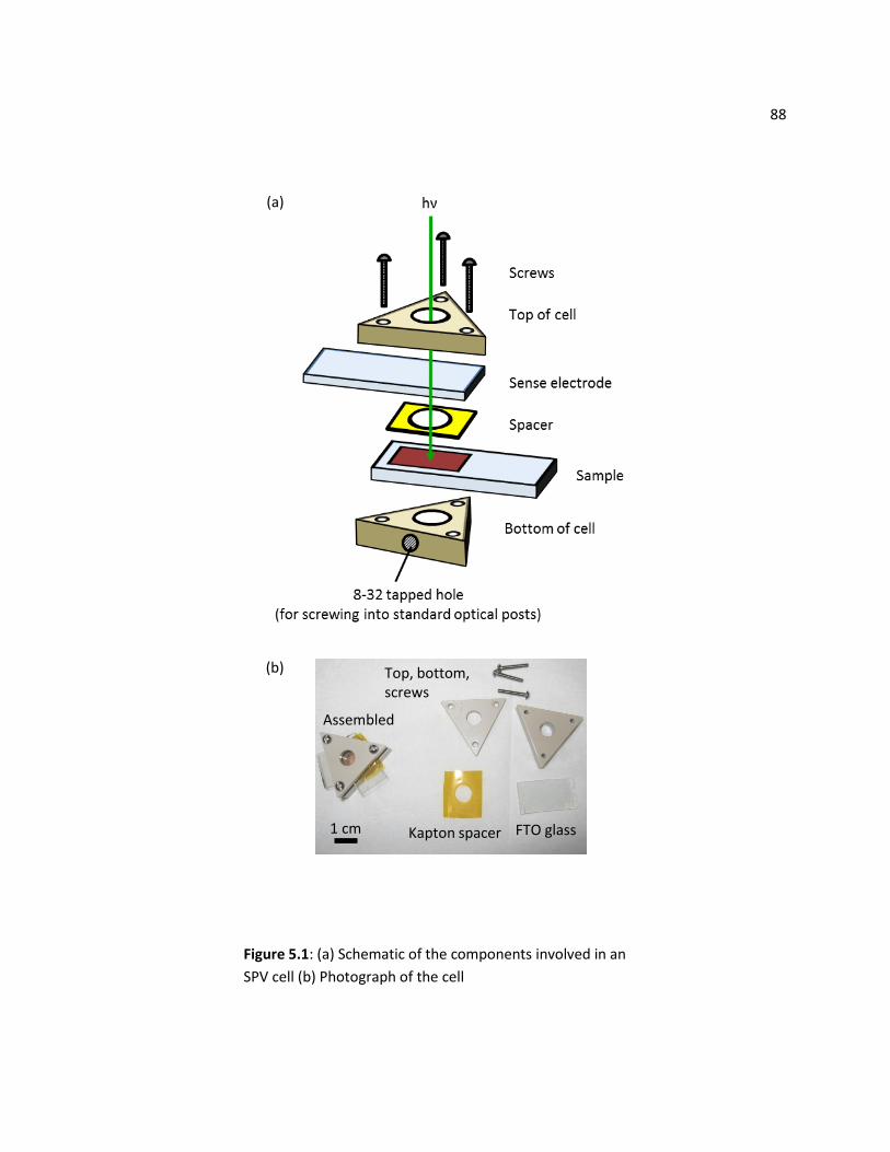
88
Figure 5.1: (a) Schematic of the components involved in an
SPV cell (b) Photograph of the cell
Kapton spacer
Assembled
FTO glass
Top, bottom, screws
1 cm
(b)
(a)

89 capacitor electrodes). Exposure of the samples to air was successfully prevented by either (1)
performing the experiment in a nitrogen-purged flow cell, or (2) pre-assembling the cell in an Ar-filled
glovebox. Screwing the entire cell together made a tight seal around the open space, preserving the
inert environment between the electrodes. The second approach would not work if one were to use a
metal mesh as the sense electrode (e.g. for experiments involving UV or NIR light).
5.3 Steady-state SPV Experiments
In the case of steady-state measurements, samples were irradiated with light sourced from a
250W quartz-tungsten-halogen lamp (Newport Model 66884) that was focused into a scanning
monochromator (Acton SpectroPro-275, grating blazed at 500 nm). The light beam was mechanically
chopped (Thorlabs MC1000-A) to enable lock-in detection. An additional filter was added to remove the
UV light (< 400 nm) generated from second order diffraction processes of the monochromator. The SPV
signal was measured with a Stanford Research Systems lock-in amplifier (SRS830 DSP). Figure 5.2(a)
shows a schematic of the setup. A pre-amplifier (Femto DLPCA-200) was sometimes used to increase
signal sensitivity. To normalize the signal from the lamp intensity profile across the wavelength range, a
pyroelectric detector (Spectrum SPH-21) was used.
This steady-state SPV technique can be used to obtain bandgap characteristics of
semiconductors. Figure 5.2(b) shows the SPV spectrum of an n-type GaP(100) single crystal doped with
sulfur (spacer used: 25 μm thick Surlyn sheet, sense electrode: FTO glass, chopping frequency = 100 Hz).
GaP is a semiconductor that has an indirect bandgap of 2.22 eV (558 nm). Accordingly, we observed an
onset of SPV signal at about 550 nm. The spectrum has two distinct regions, a shallow tail (460 – 550
nm) and a steep increase (wavelengths below 460 nm), which correspond to the indirect and the direct
(at 2.78 eV or 446 nm) gaps of the GaP crystal respectively.6
In the case of sensitized systems or heterostructures, SPV measurements can be used to detect
charge transfer across the interface. Figure 5.2(c) shows the SPV spectrum of CdSe quantum dots (QDs)
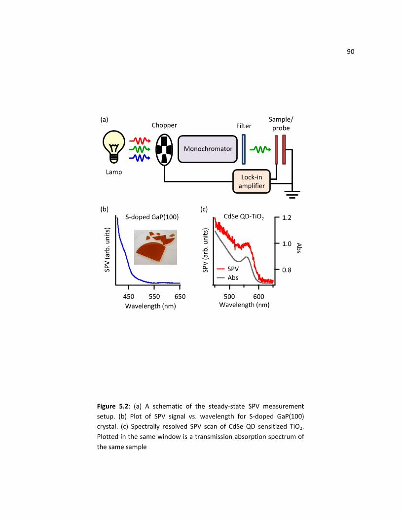
90
Sample/probeChopper
Monochromator
Lock-in amplifier
Lamp
Filter(a)
S-doped GaP(100)
650550450
SPV
(ar
b. u
nit
s)
Wavelength (nm)
(b)CdSe QD-TiO2
(c)SP
V (
arb
. un
its)
600500Wavelength (nm)
1.2
1.0
0.8
Ab
s
SPVAbs
Figure 5.2: (a) A schematic of the steady-state SPV measurement
setup. (b) Plot of SPV signal vs. wavelength for S-doped GaP(100)
crystal. (c) Spectrally resolved SPV scan of CdSe QD sensitized TiO2.
Plotted in the same window is a transmission absorption spectrum of
the same sample
91 attached to a TiO2 nanocrystalline film on FTO with a bifunctional mercaptopropionic acid linker
(assembled in an Ar-filled glovebox, spacer used: 25 μm thick Kapton sheet, dodecane gap, sense
electrode: FTO glass, chopping frequency = 590 Hz, Femto amplifier at x105 V/A gain, low speed).
Preparation of the CdSe-TiO2 sample is described elsewhere in this thesis (see Chapter 2). Also included
in the figure is the visible absorption spectrum of the sample. The CdSe QD starts to absorb at 600 nm
and has peak at ~560 nm, corresponding to the first exciton transition. The SPV signal matches the
absorption spectrum of the CdSe well. This shows that optical excitation of the CdSe QDs results in a
spatial separation of charge on the CdSe-TiO2 sample. It is not possible to generate SPV signals
separately from CdSe QDs (there is no band bending effects due to their small sizes) or from TiO2 (its
bandgap is in the UV). The energy level of the conduction band of the CdSe QDs is such that it can
transfer electrons into the conduction band of the TiO2.7 Therefore, the measured SPV signal comes
from the charge transfer and charge separation at the interface of CdSe and TiO2. This SPV technique is a
convenient way to verify presence of charge transfer in sensitized systems and heterostructures.
5.4 Transient SPV Experiments
Instead of using a continuous light source, SPV measurements can also be performed with
pulses of light. If the timescale for the dynamics of charge separation is longer than the pulse duration, it
is possible to extract time-resolved information of the SPV. This section focuses on transient SPV
experiments with nanosecond pulses.
The schematic for the transient SPV setup is shown in Figure 5.3(a). Pulses from a commercially
purchased tunable laser (Ekspla NT342B-SH, third harmonic (355 nm) generation from Nd:YAG with an
optical parametric oscillator, tunable from 210 to 2300 nm, ~3 ns pulse duration) served as our light
source. The intensity of the laser pulses was controlled by the angle of a polarizer and was measured
with a pyroelectric detector (Coherent EnergyMax sensor). The SPV transients were amplified first (Fast
ComTec model TA2000B-3, a unit in AC mode giving 40x amplification, or model TA2000B-1, a unit in DC

92 mode giving 10x amplification, both models have 50 Ω input and output impedances), and then were
recorded with a digital oscilloscope (Agilent Model DSO5054A). A Faraday cage enclosed the sample cell
and amplifier setup; it was necessary to minimize the external electromagnetic interference, especially
when dealing with small SPV signals. It is important to note how the two electrodes are connected to
the amplifier/oscilloscope, since this affects the sign of the transient signal. All data in this section is
presented with the sample connected to ground, as illustrated in Figure 5.3(a). If the electrodes were
flipped (i.e. sense electrode connected to ground), then the sign of the transients we observe would be
the opposite of what is shown here.
The sign of the transient signals is indicative of the sign of charge that is accumulated on the
surface; this could be valuable information especially when dealing with less well-studied materials of
unknown doping type. Figure 5.3(b) illustrates this sign dependence with highly doped p-type and n-
type Si(111) samples (boron doped for p-type, phosphorus doped for n-type, both have resistivity values
of 0.001 - 0.004 Ω·cm, and were purchased from Addison Engineering). The Si piece was contacted
through the back with either Pt foil (for the p-type sample) or Zr foil (for the n-type sample). The spacer
used was 127 μm thick Teflon sheet, sense electrode was FTO glass, and the laser was at 700 nm with
0.1 mJ/cm2 per pulse. For both samples, we observed an initial rise of the signal, and then a recovery
with an opposite sign. This shape of the transient is interpreted as the capacitive charging (the rise) and
discharging (the recovery) of the charges generated in the sample-sense electrode system. This
displacement current from the capacitive charging and discharging was observed due to the relatively
small input impedance (50 Ω) of the oscilloscope. The timescales of the transient signal depend on the
different equivalent RC time constants (established by contact resistances, sample internal space charge
layer, and external capacitive-like arrangement of the system). The analysis of the relationship between
the RC time constants, and the timescales of the signal observed will be discussed in more detail later.
The n-type Si sample initially exhibited a positive signal, corresponding to the accumulation of positive
93 charges at the surface due to the nature of the band banding at the surface (see chapter 1). Conversely,
the p-type sample gave an initial negative signal, due to negative charge accumulation at the surface.
As with steady-state SPV spectroscopy discussed in the previous section, the transient SPV
technique can be used to obtain spectral information with the use of a tunable laser as the light source.
The increased intensity from the laser (as opposed to a tungsten lamp coupled to a monochromator) can
give larger SPV signals in weakly absorbing materials. However, the incident intensity of light should not
be too intense of course – we wouldn’t want to destroy the sample! We show in Figures 5.3(c) – (e) that
this spectrally resolved transient SPV technique can characterize charge transfer across heterostructures
as well as determine the doping type and optical band gap of novel nanostructures. Transient signals
were collected at intervals of wavelengths, then the peak heights or peak areas from each trace were
obtained and plotted against wavelength. Using peak areas is more accurate, as this capacitive
measurement produces a photocurrent, and the peak area is then proportional to the total charge
separated upon excitation.
Figure 5.3(c) shows transient signals from a sample of CdSe-TiO2 heterostructure on FTO glass
(see above section for sample preparation details) at three different wavelengths, while Figure 5.3(d)
shows the peak height (from each transient) plotted versus wavelength. Also included in this Figure (d) is
the transmission absorption spectrum of the sample. In this spectrally resolved figure, the points for λ >
600 nm were artificially set to zero; although the transient data was collected, there was no detected
SPV signal. This CdSe-TiO2 transient SPV data matched the absorption spectrum, indicating charge
transfer (and spatial charge separation) across the heterostructure. The information obtained from this
experiment is similar to the steady state SPV experiment. However, here we can additionally verify the
type of charge that is localized on the surface. (We note that the determination of charge type can be
achieved with steady state SPV experiments via the CPD/Kelvin Probe method, but not via MIS
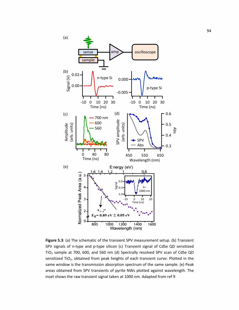
94
Figure 5.3: (a) The schematic of the transient SPV measurement setup. (b) Transient
SPV signals of n-type and p-type silicon (c) Transient signal of CdSe QD sensitized
TiO2 sample at 700, 600, and 560 nm (d) Spectrally resolved SPV scan of CdSe QD
sensitized TiO2, obtained from peak heights of each transient curve. Plotted in the
same window is the transmission absorption spectrum of the same sample. (e) Peak
areas obtained from SPV transients of pyrite NWs plotted against wavelength. The
inset shows the raw transient signal taken at 1000 nm. Adapted from ref 9
oscilloscopeamp
sample
sense
Am
plit
ud
e(a
rb. u
nit
s)
80400Time (ns)
700 nm600560
SPV
am
plit
ud
e(a
rb. u
nit
s)
650550450Wavelength (nm)
0.6
0.5
0.4
0.3
Ab
s
SPVAbs
n-type Si
p-type Si
(a)
(b)
(c) (d)
(e)
Sign
al (
V) 0.02
0.00
3020100-10
-0.005
0.000
3020100-10Time (ns) Time (ns)
λ=1000 nm
20100-10
-1.0
-0.5
0.0
Time (ns)
Sign
al
95 measurement method). The observation of the positive transient signal indicates that holes are trapped
on the surface (i.e. the CdSe QDs), in agreement with the band alignments of CdSe QDs and TiO2.7
We have also successfully used this technique to characterize novel semiconductor
nanostructures of hematite (α-Fe2O3)8 and iron pyrite (FeS2).
9 Iron pyrite is an earth abundant material
that has a lot of potential in photovoltaic applications due to its high absorption coefficient and the well-
matched bandgap (0.95 eV) to the output from the sun. However, there are still challenges to making an
efficient photovoltaic material. Bringing materials down to the nanoscale has additional advantages,
primarily the increased surface area and smaller distances for the charge carriers to travel and be
collected. The delicate thin films of these pyrite nanowires (NWs) make it challenging for optical
bandgap determination with conventional absorption spectroscopy. Figure 5.3(e) shows the spectrally
resolved transient SPV measurements of pyrite NWs grown on stainless steel (spacer: two 75 μm thick
Teflon sheets, sense: semitransparent Cr electrode, made by evaporating 5 nm Cr on glass, 40x
amplifier). This figure plots the peak area calculated from each transient versus wavelength. The inset
shows the raw data at λ = 1000 nm. The surface sensitive, non-contact nature of the SPV measurement
made it possible for us to extract the bandgap of these NWs and show that they matched the known
values of pyrite. Additionally, from the negative sign of the transient signal, these NWs were determined
to exhibit p-type doping. This p-type behaviour is commonly seen in thin films of pyrite, but not in
natural single crystals of pyrite (which are n-type). We also observed signals at sub-bandgap
illumination, indicating defect or trap states on the surface of these NWs.9
Extracting timescales with this technique is not straightforward, as there are various RC time
constants associated with the SPV system. Figure 5.4(a) shows an equivalent circuit model of the SPV
measurement. The transient SPV signal is represented as a battery with a time-controlled switch. The
battery simulates the illumination-induced generation of photocurrent from the material, while the
switch terminates this current after a specified period of time (tSW) simulating the transient light pulse
96 and recombination of the separated charges. The semiconducting material has a space charge layer,
represented as a capacitance, Csc, and a charge carrier recombination resistance, Rrecom. The space
charge capacitance and recombination resistance make up an RC time constant, which we will call the
recombination time constant, tr = Rrecom*Csc. Additionally, there are external contact resistances and the
sample internal resistance; these values are collectively represented as Rc in the diagram. The capacitor-
like arrangement of the SPV measurement here (from the MIS structure formed by the sample,
insulating gap, and sense electrode) is shown as Cgap. Finally, we have the impedance of the oscilloscope
(either 50 Ω or 1 MΩ), shown as Rmeas. Another RC time constant is established outside of the
semiconductor space charge layer by the MIS structure. We will call this tMIS = (Rc + Rmeas)*Cgap.
Simulations of the transient signal were performed with TINA-TI v9 (Texas Instruments). For
simplicity, we make the switch time, tSW to be equal to τr, and redefine it as tSPV (= tSW τr) in all cases
shown here. Cgap depends on the spacer used, and can be calculated using C εrε0A/d, where εr is the
dielectric constant, ε0 is the vacuum permittivity = 8.854 x 10⁻¹² Fm-1, A is the overlap area of the two
plates, and d is the separation between plates. For εr 1 (for air), A π*(0.5 cm)2, and d 100 μm, we
have C ~ 7 pF. For the simulation (and simplicity), we will set Cgap = 10 pF, and also assume Rc 100 Ω.
Using these values, we obtain tMIS = 1.5 ns at an oscilloscope impedance of 50 Ω, and tMIS 10 μs at
oscilloscope impedance of 1 MΩ.
Figures 5.4(b) – (d) show the results of the simulations at a range of SPV timescales: tSPV = 100
ps, 1, 10, and 100 ns. Qualitatively, we observed the positive rise and negative recovery in the signal,
coming from the charging and discharging of the capacitive currents in the circuit. Next to each trace in
the figures, the exponential time constants, τ, from fitting the negative part of the signal for the
corresponding tSPV are shown. Several observations can be made: First, if tSPV << tMIS, as shown in the tSPV
100 ps case, τ tMIS, the recovery time constant is just dictated by the discharge of the capacitor-like
MIS setup. Second, if tSPV ≈ tMIS, τ is a complicated sum of both tSPV and tMIS. This is illustrated in the tSPV =
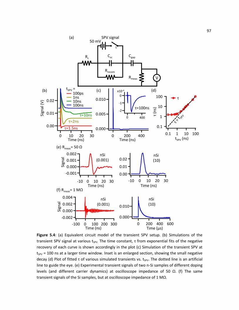
97
Figure 5.4: (a) Equivalent circuit model of the transient SPV setup. (b) Simulations of the
transient SPV signal at various tSPV. The time constant, τ from exponential fits of the negative
recovery of each curve is shown accordingly in the plot (c) Simulation of the transient SPV at
tSPV = 100 ns at a larger time window. Inset is an enlarged section, showing the small negative
decay (d) Plot of fitted τ of various simulated transients vs. tSPV. The dotted line is an artificial
line to guide the eye. (e) Experimental transient signals of two n-Si samples of different doping
levels (and different carrier dynamics) at oscilloscope impedance of 50 Ω. (f) The same
transient signals of the Si samples, but at oscilloscope impedance of 1 MΩ.
τ=100ns
SPV signal
Csc
Rrecom
CgapRc
Rmeas V
t
50 mV
τ=1.5ns
τ=2ns
τ=10ns
(a)
(b) (c) (d)
0.02
0.01
0.00
3020100
tSPV = 100ps 1ns10ns 100ns
Sign
al (
V)
Time (ns)
0.010
0.005
0.000
4002000
-2
-1
0
4000
x10-4
0.1
1
10
100
τ(n
s)
0.1 1 10 100tSPV (ns)
τ
Time (ns)
nSi(0.001)
nSi(10)
(e) Rmeas= 50 Ω
(f) Rmeas= 1 MΩ
nSi(0.001)
nSi(10)
0.002
0.001
0.000
-0.001
3020100-10
0.02
0.01
0.00
3020100-10
0.004
0.002
0.000
-0.002
3002001000-100
0.010
0.000
6004002000
Time (ns) Time (ns)
Time (ns) Time (μs)
Sign
alSi
gnal

98 1 ns case; the fitted τ was ~2 ns. Third, if tSPV >> tMIS, τ tSPV, as shown in the tSPV, = 10 and 100 ns traces.
Figure 5.4(d) shows a plot of fitted τ vs. tSPV obtained from a range of simulated transients. This shows
that to experimentally obtain the true tSPV, we must make sure that the SPV timescale is at least 10x
larger than tMIS. However, to maintain electrical neutrality, the peak areas of the positive rise and
negative recovery must remain equal. Therefore, a large tSPV would have a small negative peak height, as
illustrated in Figure 5.4(c) for the tSPV = 100 ns case (as the negative feature is more spread out in time).
The negative peak is barely visible at full scale, but the enlarged section in the inset clearly shows the
small negative decay, with τ 100ns.
We can experimentally see this effect of SPV timescales by comparing n-type Si of two different
doping levels: sample (1) has resistivity of ~0.001 Ω·cm (‘nSi_0.001’) and sample (2) resistivity of ~10
Ω·cm (‘nSi_10’). Figures (c) and (d) show the transient signal of the Si samples. As expected, the highly
doped sample has a shorter lifetime, as we can observe the negative signal immediately after the
positive rise. For the less doped sample, we only observed the rise, but we could not detect the negative
decay, even at longer times. We can further verify this by changing the oscilloscope impedance to 1 MΩ.
The tMIS is estimated to be ~10 μs at Rc = 100 Ω. The transient signals are shown in Figures (e) and (f). For
the highly doped Si, only oscillations due to mismatched sample/scope impedances were observed.
However, for the less-doped sample, we observed a positive decay in the microsecond region, and a
small negative recovery. Since the contact resistance of this sample is unknown, it is unclear whether
this positive decay is from the SPV process or from the MIS time constant.
In conclusion, this transient SPV technique with a nanosecond-pulsed laser is an alternative
method to obtain spectrally resolved information, and can give better signal sensitivity when compared
to the steady-state SPV measurement. However, it may be challenging to extract timescales from this
technique, due to the presence of two time constants (tSPV and tMIS) that affects the observed transient.
One would also have to accurately know the sample and contact resistances, as well as take into
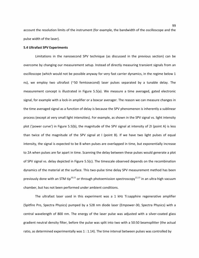
99 account the resolution limits of the instrument (for example, the bandwidth of the oscilloscope and the
pulse width of the laser).
5.4 Ultrafast SPV Experiments
Limitations in the nanosecond SPV technique (as discussed in the previous section) can be
overcome by changing our measurement setup. Instead of directly measuring transient signals from an
oscilloscope (which would not be possible anyway for very fast carrier dynamics, in the regime below 1
ns), we employ two ultrafast (~50 femtosecond) laser pulses separated by a tunable delay. The
measurement concept is illustrated in Figure 5.5(a). We measure a time averaged, gated electronic
signal, for example with a lock-in amplifier or a boxcar averager. The reason we can measure changes in
the time averaged signal as a function of delay is because the SPV phenomenon is inherently a sublinear
process (except at very small light intensities). For example, as shown in the SPV signal vs. light intensity
plot (‘power curve’) in Figure 5.5(b), the magnitude of the SPV signal at intensity of 2I (point A) is less
than twice of the magnitude of the SPV signal at I (point B). If we have two light pulses of equal
intensity, the signal is expected to be B when pulses are overlapped in time, but exponentially increase
to 2A when pulses are far apart in time. Scanning the delay between these pulses would generate a plot
of SPV signal vs. delay depicted in Figure 5.5(c). The timescale observed depends on the recombination
dynamics of the material at the surface. This two-pulse time delay SPV measurement method has been
previously done with an STM tip10,11 or through photoemission spectroscopy12,13 in an ultra-high vacuum
chamber, but has not been performed under ambient conditions.
The ultrafast laser used in this experiment was a 1 kHz Ti:sapphire regenerative amplifier
(Spitfire Pro, Spectra Physics) pumped by a 528 nm diode laser (Empower-30, Spectra Physics) with a
central wavelength of 800 nm. The energy of the laser pulse was adjusted with a silver-coated glass
gradient neutral density filter, before the pulse was split into two with a 50:50 beamsplitter (the actual
ratio, as determined experimentally was 1 : 1.14). The time interval between pulses was controlled by
100
Figure 5.5: (a) An illustration of the ultrafast SPV measurement utilizing
two pulses delayed in time from one another, and the expected signal
from the various regimes of delay time (b) Plot of SPV signal vs. light
intensity, showing the sublinear nature of the SPV phenomenon (c) The
signal that we would expect as a function of delay (d) Schematic of the
ultrafast SPV measurement setup
t2 = t1 t2 > t1 t2 >> t1
t1
t2
t1
t2
t t t
signal = 2Asignal = B B < signal < 2A
t1
t2
2A
B
delay
Sign
al
0
SPV
sign
al
Intensity
A
B
I 2I
(a)
(b) (c)
(d)
boxcarampsample
sensediode
∆t
101 directing one of the beams into an optical delay line composed of a retroreflector mounted on a 300
mm-long linear translation stage (Thorlabs LTS300). Both beams were then collected and directed
through the transparent sense electrode and into the sample. Auto-correlation of the two pulses with a
piece of BBO crystal yielded a Gaussian width of about 150 fs.
As shown in Figure 5.5(d), the capacitor-like setup of the sample-sense electrodes was first
connected to pre-amplifiers (two 10x Fast ComTec Model TA2000B-1 connected in series, resulting in
100x gain), then a fast diode (Model 203A from Krytar, 10 MHz – 20 GHz zero bias Schottky detector
operating at negative polarity) before connecting to a boxcar averager system (Stanford Research
Systems Model SR250). The diode was needed since this technique relies on a time-averaged detection
method; the raw transient signal has capacitive charge-discharge peaks that would average out to zero.
Figures 5.6(a) and (b) show the transient signal on the oscilloscope with and without the diode
respectively on an n-type InP sample. Since this is a negative bias diode, all connections in this ultrafast
SPV section were made such that we obtain negative signal rectification (for n-type semiconductor,
sense electrode to ground, but for p-type semiconductor, sample to ground). We note that no signal (as
observed on the scope) was detected if the electrodes were connected the other way. All data was
taken using a piece 127 μm-thick Teflon piece as the spacer, and a piece of ITO glass (30 – 60 Ω/sq,
Sigma-Aldrich product 703184) as the sense electrode. To make sure the contacts were ohmic, Pt foil
was used as the back contact for p-type samples, while Zr foil was used for n-type samples.
We successfully demonstrated fast dynamics in a few highly-doped semiconductors with this
technique. First we must make sure that the sum of light intensity of the two pulses does not lie within
the linear regime of the power curve. Figure 5.6(c) shows the SPV signal (as measured by the boxcar
averager) vs. the power of a single pulse for the n-InP sample. Figures 5.6(d) shows the delay scan of the
n-InP sample with one of the beams at 3 mW power, and the other at 3.4 mW (as measured by a
ThorLabs S120VC Si-photodiode detector). Fitting the positive half of the delay to an exponential yielded
102 a time constant of 870 ps. We also measured a p-type GaAs sample, as shown in Figure 5.6(e), with 4
and 4.6 mW pulse powers. The p-GaAs delay scan has a time constant of 1.9 ns. Both crystals were
obtained from Institute of Electronic Materials Technology (ITME). The n-type InP(100), doped with S,
has a resistivity of 6.5 x 10⁻⁴ Ω·cm and a carrier concentration of 8.3 x 1018 cm-3. The p-type GaAs(100),
doped with Zn+In, has a resistivity of 0.0525 - 0.0738 Ω·cm and a carrier concentration (4.7-7.3) x 1017
cm-3. These resistivity and carrier concentration values were obtained from the manufacturers.
We have utilized this technique to monitor the effect of surface treatment on a semiconductor.
Iron pyrite (FeS2), a cheap, earth abundant semiconductor is currently studied as a possible material for
harvesting solar energy for photoelectrochemical applications. However, one of the major challenges in
practical utilization of pyrite is the fast recombination lifetimes due to the large concentration of defect
and trap states in the material. Surface treatments can change carrier lifetimes of pyrite and gaining an
understanding of how different surface treatment affect the carrier lifetime is important for the
development of practical pyrite devices.4 This ultrafast SPV technique can provide a convenient
technique to measure carrier dynamics of pyrite. Here we have successfully measured the SPV
recombination lifetimes of single crystal natural pyrite.
Slices of pyrite sample (~2 mm thick) were cut from the faces of a single crystal natural
pyrite(100) cube with a rotating diamond saw. The samples were then cleaned with deionized water (DI
H2O), acetone, carbon tetrachloride and dichloromethane via sonication. From the sign of the transient
SPV signal on the oscilloscope, the natural pyrite samples exhibited n-type behaviour. This doping type is
consistent with what was previously observed by others using non-SPV measurement techniques.14
Figure 5.6(f) – (h) show the scans of SPV signal of a pyrite sample as a function of delay between pulses,
at 10 and 11.4 mW laser powers, before and after various treatments. The as-prepared sample on Figure
(f) shows a fitted exponential time constant of 420 ps. The sample was then subjected to a polishing
procedure: 2 min with 0.05 μm-sized suspension of alumina particles, then 3 min with 0.02 μm-sized

103
Figure 5.6: (a) Transient signal without diode (b) Transient signal with diode, showing
that only the negative signal was detected (c) Plot of integrated signal from the boxcar
vs. power of one of the pulses (d)-(h) Signal plotted as a function of delay of (d) the n-
InP(100) sample (e) p-GaAs(100) sample (f) as-prepared natural pyrite (g) polished pyrite
(h) electrochemically treated pyrite. The natural pyrite sample showed n-type behaviour
in all cases.
τ=870ps
n-InP(100)
τ=1.9ns
p-GaAs(100)
(a) (b) (c)
(d) (e)
(f) As-prepared (g) Polished (h) Electrochemically treated
-0.4
-0.2
0.0
0.2
40200
-0.02
-0.01
0.00
40200
-0.15
-0.10
-0.05
0.00
6420
Sign
al
Bo
xcar
sign
al
Time (ns) Time (ns) Power (mW)
Without diode
With diode
n-InP n-InP
τ=420ps τ=120ps τ=440ps
-0.30
-0.29
-0.28
8004000-400
Sign
al
-0.56
-0.54
-0.52
10005000Time (ps) Time (ps)
-0.24
-0.22
-0.20
10005000
-0.28
-0.26
-0.24
10005000
-0.22
-0.20
10005000Time (ps) Time (ps) Time (ps)

104 suspension of silica particles. The sample was rinsed thoroughly and sonicated with DI H2O in between
steps and after polishing. As shown in Figure (g), the polished sample exhibited a lifetime of 120 ps, a
decrease from the freshly prepared sample. This decrease in lifetime could indicate that the polishing
procedure introduced more defect and trap states into the crystal, thus decreasing effective carrier
lifetime of the sample. We subsequently performed an electrochemical treatment on the same sample
that was previously found to passivate pyrite crystals. This procedure involves reducing H2SO4 to H
atoms that can diffuse into the pyrite crystal to passivate defects.15-18 Figure (h) shows the resulting
delay scan of the treated pyrite sample. We obtained a time constant of 440 ps, an increase from the
polished sample (back to within ~5 % of the original value), indicating some passivation of the sample
has occurred. Using the ultrafast technique, we can track the effects of surface treatment on the carrier
lifetimes of pyrite. We found that the polishing treatment was detrimental to the crystal, and led to a 71
% decrease in the carrier lifetime. However, the electrochemical treatment led to a recovery of the
lifetime, as a result of passivation of the defects in the crystal.
5.5 Conclusions
SPV is a non-contact, non-destructive technique to conveniently measure spatial separation of
charges within a material, or across the interface of a heterojunction. Steady-state SPV experiments can
provide information on the bandgap of a semiconductor, and the evidence of charge transfer between a
sensitized system. Transient experiments can be similarly used to inform us about the spectral
dependence of the SPV signal. Additionally, we can also find out which type of charge is localized on the
surface from the sign of the transient signal. Obtaining SPV timescales from a single-pulse experiment is
potentially challenging, as the RC time constant from the MIS capacitive measurement setup plays a
large role in the timescales measured from the oscilloscope. We have further developed an ultrafast SPV
technique to overcome the limitations of the single-pulse experiments that involves irradiating the
sample with two ultrafast pulses delayed from one another. With this technique, we were able to
105 measure SPV recombination timescales of highly doped n-type InP and p-type GaAs single crystals, as
well as natural iron pyrite crystals. We further measured the effect of surface treatments on these pyrite
samples, and found that polishing the sample introduces more defects to the sample, but the defects
were potentially passivated with an electrochemical treatment.
5.6 References
1. Kronik, L.; Shapira, Y. Surface photovoltage phenomena: Theory, Experiment, and Applications, Surf. Sci. Rep. 1999, 37, 1-206.
2. Zhang, J. Z. Interfacial Charge Carrier Dynamics of Colloidal Semiconductor Nanoparticles, J. Phys. Chem. B 2000, 104, 7239-7253.
3. Katz, M. J.; Riha, S. C.; Jeong, N. C.; Martinson, A. B. F.; Farha, O. K.; Hupp, J. T. Toward Solar Fuels: Water Splitting with Sunlight and "Rust"?, Coord. Chem. Rev. 2012, 256, 2521-2529.
4. Steinhagen, C.; Harvey, T. B.; Stolle, C. J.; Harris, J.; Korgel, B. A. Pyrite Nanocrystal Solar Cells: Promising, or Fool's Gold?, J. Phys. Chem. Lett. 2012, 3, 2352-2356.
5. Kronik, L.; Shapira, Y. Surface photovoltage spectroscopy of semiconductor structures: at the crossroads of physics, chemistry and electrical engineering, 2001, 31, 954-965.
6. Strehlow, W. H.; Cook, E. L. Compilation of Energy Band Gaps in Elemental and Binary Compound Semiconductors and Insulators, J. Phys. Chem. Ref. Data 1973, 2, 163-193.
7. Kamat, P. V. Quantum Dot Solar Cells. Semiconductor Nanocrystals as Light Harvesters, J. Phys. Chem. C 2008, 112, 18737-18753.
8. Li, L.; Yu, Y.; Meng, F.; Tan, Y.; Hamers, R. J.; Jin, S. Facile Solution Synthesis of α-FeF3·3H2O Nanowires and Their Conversion to α-Fe2O3 Nanowires for Photoelectrochemical Application, Nano Lett. 2012, 12, 724-731.
9. Caban-Acevedo, M.; Faber, M. S.; Tan, Y.; Hamers, R. J.; Jin, S. Synthesis and Properties of Semiconducting Iron Pyrite (FeS2) Nanowires, Nano Lett. 2012, 12, 1977-1982.
10. Terada, Y.; Yoshida, S.; Takeuchi, O.; Shigekawa, H. Real-Space Imaging of Transient Carrier Dynamics by Nanoscale Pump-Probe Microscopy, Nat. Photonics 2010, 4, 869-874.
11. Hamers, R. J.; Cahill, D. G. Ultrafast Time Resolution in Scanned Probe Microscopies, Appl. Phys. Lett. 1990, 57, 2031-2033.
12. Tokudomi, S.; Azuma, J.; Takahashi, K.; Kamada, M. Ultrafast time dependence of surface photo-voltage effect on p-type GaAs(100) surface, J. Phys. Soc. Jpn. 2008, 77.

106 13. Sezen, H.; Ozbay, E.; Aktas, O.; Suzer, S. Transient Surface Photovoltage in n- and p-GaN as
Probed by X-Ray Photoelectron Spectroscopy, Appl. Phys. Lett. 2011, 98.
14. Ennaoui, A.; Fiechter, S.; Pettenkofer, C.; Alonsovante, N.; Buker, K.; Bronold, M.; Hopfner, C.; Tributsch, H. Iron Disulfide for Solar-Energy Conversion, Sol. Energy Mater. Sol. Cells 1993, 29, 289-370.
15. Alonsovante, N.; Chatzitheodorou, G.; Fiechter, S.; Mgoduka, N.; Poulios, I.; Tributsch, H. Interfacial Behavior of Hydrogen-Treated Sulfur Deficient Pyrite (FeS2-x), Sol. Energy. Mater. 1988, 18, 9-21.
16. Buker, K.; Alonsovante, N.; Scheer, R.; Tributsch, H. Influence of Electrochemical Activation and Surface Orientation on the Photoresponse of Single-Crystalline Pyrite Electrolyte and Pyrite Metal Junctions, Ber. Bunsen. Phys. Chem. 1994, 98, 674-682.
17. Bungs, M.; Tributsch, H. Electrochemical and photoelectrochemical insertion and transport of hydrogen in pyrite, Ber. Bunsen. Phys. Chem. 1997, 101, 1844-1850.
18. Bronold, M.; Buker, K.; Kubala, S.; Pettenkofer, C.; Tributsch, H. Surface Preparation of FeS2 via Electrochemical Etching and Interface Formation with Metals, Phys. Status Solidi A 1993, 135, 231-243.
107
Chapter 6
Conclusions and Outlook
There is great potential for nanostructured materials such as chalcogenide quantum dots or
earth abundant iron pyrite for applications in photovoltaic or photoelectrochemical devices to enable
cheap, efficient energy conversion from the sun. However, there are still a lot of challenges that needs
to be faced. In this thesis, we have only attempted to address a part of the problem.
We first explored the issue of chemical instability of chalcogenide quantum dots (QDs) and its
relationship to the electronic structure of the capping ligands. Ligands play a large role in the
photostability and electronic properties of quantum dots. We surprisingly found that the use of small
conjugated organic ligands can passivate QDs, much more so with ligands bearing electron-donating
substituents. There are many opportunities to which our work can be expanded. As briefly studied here,
one is to further explore more ligand designs, especially those that could be used for PbS and PbSe QDs.
Furthermore, our work has largely been of fundamental science; we have yet to utilize this ligand
passivation idea fully into a working solar cell. I imagine that we could incorporate these QDs with
electron-donating ligands into a polymer or a solid state solar cell to enhance the photostability of these
devices.
The other part of my thesis is development of measurement methods to enable the study of
these nanostructured materials. Transient surface photovoltage (SPV) methods, particularly ultrafast
SPV, have a lot of potential for the measurement of fast carrier dynamics in materials and
heterostructures that are relevant for photovoltaic or photoelectrochemical cells. The ultrafast SPV
work done in this thesis has only explored carrier relaxation times, but one could possibly extend this
method to measure fast charge injection dynamics across heterostructures. I am also especially excited
about the proposed future work of combining the ultrafast SPV method with an AFM to allow for

108 nanometer spatial resolution – we can potentially measure charge dynamics from individual quantum
dots!

109
Appendix
A1 Molecular Coverage Calculations from XPS Data for Ligands on Nanoparticles
Standard coverage calculation models of a thin film on a substrate from XPS assume a flat, thick
underlying substrate such that the sample is considered laterally identical. The signal contribution from
a thin film is only from the top of the sample closest to the detector. In the planar sample case, the
photoelectrons from the underlying substrate are only attenuated and scattered through the thin film in
one direction. However, this calculation of a planar sample may not be accurate for samples of a
different geometry, such as a very small nanoparticle coated with a thin film of organic ligands. If the
nanoparticle on the order of the electron attenuation length, the standard method will yield a large
overestimation of the thin film coverage since the sample cannot be treated infinitely identical in the
lateral dimension. The organic shell surrounding the nanoparticle in the x and y direction will also
contribute to the measured signal coming from the shell.
To account for the geometry of the small nanoparticle we used
direct numerical integration to establish the relationship between XPS
peak areas and molecular coverage of the core-shell system. We modeled
the system with a CdSe sphere with 1.6 nm radius surrounded by an
organic shell of thickness t. We then used numerical integration to
theoretically calculate the expected carbon to cadmium ratio as a
function of thickness of the organic layer t. The C/Cd values can be considered as the peak area ratios
AC/ACd obtained from XPS.
We used cylindrical coordinates to describe the nanoparticle sphere, but we began the
numerical integration with a two-dimensional slice of the sphere. We first created a region of space and
divided the space into a two-dimensional array of r- and z-coordinates. In the z-direction, zero is set at

110 the bottom of the defined space farthest from the detector. We then described a circle, and assigned
the region within the circle either as the nanoparticle core or as the organic shell. All space not confined
within the circle is assigned as vacuum. Starting from z = 0 we then integrated the expected signal from
each element along the z-direction. For example, to calculate the Cd signal at a specific r-coordinate, we
first determined whether the coordinate point is comprised of CdSe core or the organic shell. If the
point is CdSe, the Cd signal is:
( ) ( )
The first term is the total Cd signal coming from a previous (z-1) element which then undergoes
a small scattering loss e-∆z/λ in the current z element. λCd,CdSe is the ineleastic mean free path (IMFP) of
the photoelectrons of Cd through CdSe. The second term is the new Cd signal from the current z-
coordinate. In this term, ρCd,CdSe is the density of Cd in CdSe.
If the current coordinate consists of the organic layer, no new Cd photoelectrons are generated,
but the total Cd signal from the previous (z-1) element is still scattered by the organic layer. The Cd
signal is then:
( ) ( )
A similar procedure is applied for the C signal, with the appropriate IMFPs. Once we obtained
the signal at the top of the defined space in the z-direction, we then integrated along the azimuthal
direction Φ at each r-coordinate, and added up the values at all r-coordinates to obtain the total Cd and
C signal from the three-dimensional core-shell structure.
From the plot of C/Cd values vs. t calculated from the numerical integration, we used the
experimentally obtained AC/ACd values from XPS (after normalizing the appropriate sensitivity factors) to
obtain an effective thickness (t) of the organic layer. This value is essentially an effective thickness and
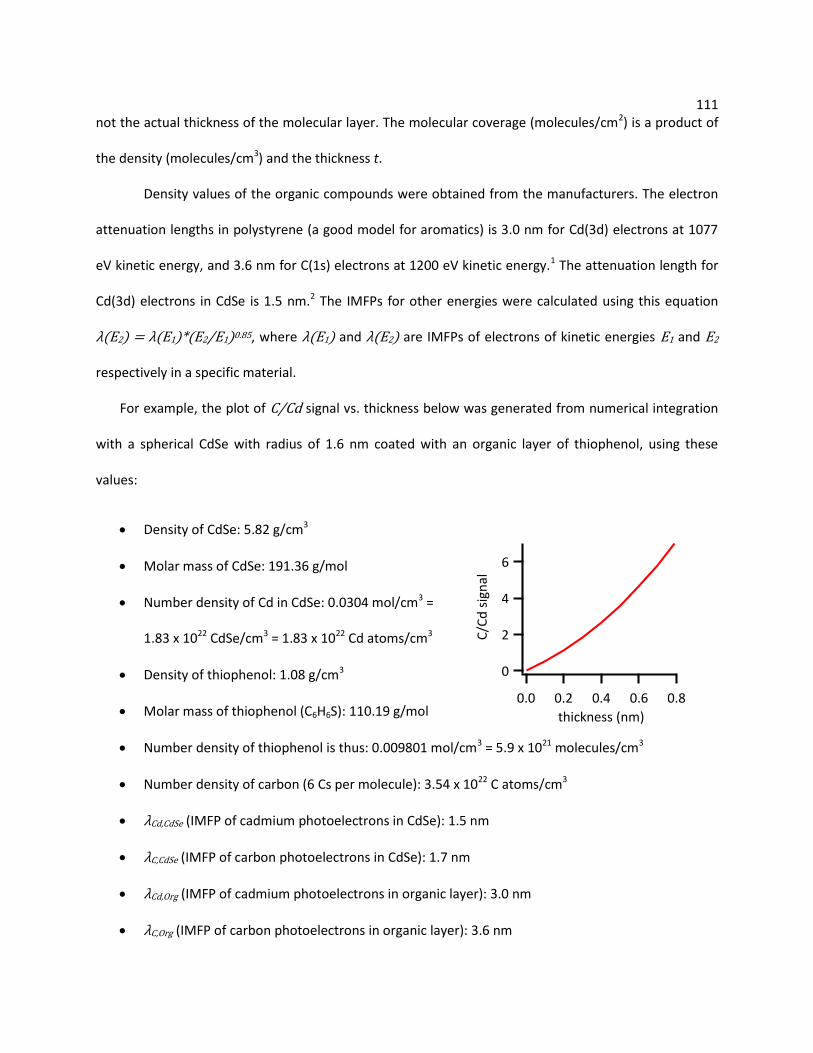
111 not the actual thickness of the molecular layer. The molecular coverage (molecules/cm2) is a product of
the density (molecules/cm3) and the thickness t.
Density values of the organic compounds were obtained from the manufacturers. The electron
attenuation lengths in polystyrene (a good model for aromatics) is 3.0 nm for Cd(3d) electrons at 1077
eV kinetic energy, and 3.6 nm for C(1s) electrons at 1200 eV kinetic energy.1 The attenuation length for
Cd(3d) electrons in CdSe is 1.5 nm.2 The IMFPs for other energies were calculated using this equation
λ(E2) λ(E1)*(E2/E1)0.85, where λ(E1) and λ(E2) are IMFPs of electrons of kinetic energies E1 and E2
respectively in a specific material.
For example, the plot of C/Cd signal vs. thickness below was generated from numerical integration
with a spherical CdSe with radius of 1.6 nm coated with an organic layer of thiophenol, using these
values:
Density of CdSe: 5.82 g/cm3
Molar mass of CdSe: 191.36 g/mol
Number density of Cd in CdSe: 0.0304 mol/cm3 =
1.83 x 10²² CdSe/cm3 = 1.83 x 10²² Cd atoms/cm3
Density of thiophenol: 1.08 g/cm3
Molar mass of thiophenol (C6H6S): 110.19 g/mol
Number density of thiophenol is thus: 0.009801 mol/cm3 = 5.9 x 10²¹ molecules/cm3
Number density of carbon (6 Cs per molecule): 3.54 x 10²² C atoms/cm3
λCd,CdSe (IMFP of cadmium photoelectrons in CdSe): 1.5 nm
λC,CdSe (IMFP of carbon photoelectrons in CdSe): 1.7 nm
λCd,Org (IMFP of cadmium photoelectrons in organic layer): 3.0 nm
λC,Org (IMFP of carbon photoelectrons in organic layer): 3.6 nm
6
4
2
0
C/C
d s
ign
al
0.80.60.40.20.0
thickness (nm)

112
The experimentally obtained Ac/ACd peak area ratio from XPS was 4.5, after correction to the
appropriate atomic sensitivity factors. From the plot above, we obtained an equivalent thickness of 0.43
nm. This thickness gives a carbon density of:
(3.54 x 10²² C/cm3)*(0.43 nm)*(10-7 cm/nm) = 1.52 x 10¹⁵ C/cm2
The molecular coverage of thiophenol on CdSe is then:
(1/6)*(1.52 x 1015 C/cm2) = 2.5 x 10¹⁴ molecules/cm2.
XPS analysis of a core-shell nanoparticle with an additional interface layer
There are situations in which the C signal from the XPS data cannot
be reliably used to obtain molecular coverage (e.g. adventitious carbon
contamination or the presence of multiple ligand types). If the ligand of
interest has a non-carbon binding head group, we can use the particular
element specific to the binding head group for quantitative XPS analysis.
Here we describe a CdSe core coated with an organic ligand that is bound to the CdSe with a sulfur-
containing functional group (e.g. thiol). In the case above, with no interface layer, we defined a region of
space divided into a two-dimensional array of r- and z-coordinates and subsequently assigned a specific
coordinate to the core, to the shell, or to vacuum. In this case, we defined an additional interface layer
between the core and the shell. We are specifically interested in how the S/Cd ratio varies as a function
of the (total) thickness of the organic layer (t).
In the case of the core-shell interface analysis, we first corrected for the fact
that the volume of the interface layer, VS, does not linearly increase with the volume of
the carbon layer, VC, i.e. the signal Sig(t) ≠ Sig(torg - tS) + Sig(tS) for a volumetric
integration. We used mass conservation, ρCVC NρSVS, to obtain the relationship between VS and VC,
where ρC is the density of carbon in a typical carbon material, ρS is the density of sulfur in a typical

113 sulfur material, and N is the stoichiometric carbon to sulfur atom ratio in the molecule. For density
values, we used the densities of polystyrene (PS) and sulfur S8 to calculate for ρC and for ρS respectively.
Using a density of 1.05 g/cm3 and a molar mass (of a monomer) of 104.144 g/mol for PS, we obtained ρC
= 4.77833 x 1026 C/cm3. Using a density of 2.07 g/cm3 and a molar mass of 8*(32.07) g/mol for sulfur, we
obtained ρS = 5.97 x 1026 S/cm3.
The relationship between VC and VS was then needed to proceed with the numerical
integration of the interface system. We first rewrote VC and VS as:
( )
( )
( )
where rCdSe is the radius of the CdSe nanoparticle core, torg is the thickness of the organic layer, and tS
is the thickness of the sulfur interface layer. We solved for VC/VS, using the mass conversation constraint
described above. Substituting VC and VS from above into the mass conservation equation:
( )
( )
( )
After getting this expression, the next step was to obtain the relationship between tS and torg, since the
numerical integration needed to be performed as a function of thickness t. The way to obtain this
relationship was to rearrange the above equation into this convenient form: c0x3 + c1x2 + c2x + c3 = 0,
in which the x variable is tS. We grouped the constants together and redefined it as A NρS/ρC. After
expanding the cubic expressions from the above equation with some TI-89 calculator magic, we
refactored the equation into the form: c0x3 + c1x2 + c2x + c3 = 0. The coefficients obtained were:

114
Once we properly factored the VC/VS equation, the cubic roots were found. Taking only the real
roots, we solved tS as a function of torg at each thickness value of the organic layer. After taking the
account of this volumetric correction, we performed similar numerical integration as described in the
previous section to obtain Cd(r,z) and S(r,z). In this case however, we needed to account for scattering
from three separate layers. We then used the relationship between S/Cd and thickness t to calculate
the molecular coverage, using a similar calculation procedure detailed above.
References
1. Seah, M. P.; Spencer, S. J. Attenuation Lengths in Organic Materials, Surf. Interface Anal. 2011, 43, 744-751.
2. Katari, J. E. B.; Colvin, V. L.; Alivisatos, A. P. X-ray Photoelectron Spectroscopy of CdSe Nanocrystals with Applications to Studies of the Nanocrystal Surface, J. Phys. Chem. 1994, 98, 4109-4117.

115 A2 Technical Design and Drawing of the Spectroelectrochemistry Cell

116
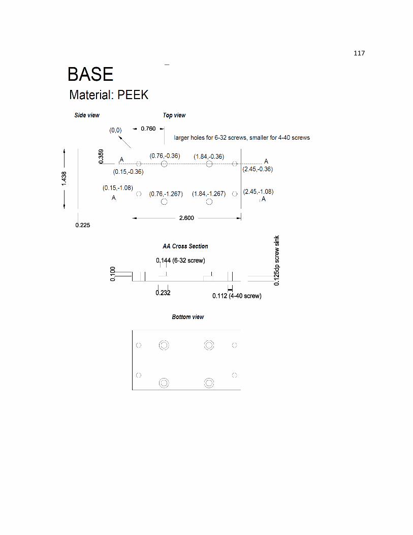
117

118 A3 Technical Design and Drawing of the SPV Cell

119
A4
Additional Data on Surface Photovoltage (SPV) Measurement
A4.1 Steady-State SPV Measurement
A4.1.1 CdSe Quantum Dot (QD) Functionalized on Doped Single Crystal Rutile (SCR) TiO2(110)1
Sample Preparation: SCR TiO2(110) samples (10x10x0.5 mm, 1 side polished, MTI corporation) were
doped by heating in a reducing environment (5% H2 in N2 gas or ‘forming gas’) at 600 C for 1 h. Samples
turned from white to greyish blue in colour. The samples were then cleaned by exposing them to the UV
lamp for 30 min. One of the sample (labeled A) were soaked in a 0.1 M 3-Mercaptopropionic Acid in
anhydrous acetonitrile (ACN) for 6 h in the dark. Sample A were then rinsed with anhydrous ACN, and
soaked in CdSe QD solution in toluene (QD diameter 3.25 nm, concentration 25 μM) overnight in the
dark. The sample was rinsed with toluene, then heptane, and was subsequently transferred into an Ar-
filled glovebox for storage. The other sample (Sample B) was designated as the bare TiO2 sample; no
further manipulation was done after the UV cleaning procedure. After cleaning, sample A was
transferred into the glovebox as well.
SPV setup: Samples (A and B) were assembled into SPV cells in the glovebox, each with a Kapton spacer
(25 μm thick) and a piece of fluorine-doped tin oxide (FTO) coated glass as the sense electrode. A piece
of Cu foil was used as the back contact for the samples. After assembly, we attempted to obtain the
absorption spectra of the samples (in reflection mode, see section 4.3.3 for optical reflection setup) but
were unsuccessful due to the low coverage of the CdSe QDs. The assembled SPV cells were placed in an
N2 purged cell during experiments to prevent CdSe photooxidation. A 250 W tungsten-halogen lamp
coupled to a monochromator served as the light source. A 400 nm cut-on filter was used. The light was
chopped at 590 Hz. Signals were pre-amplified (Femto at x105 V/A gain, low speed) before going into a
lock-in amplifier (see section 5.3 for more details).
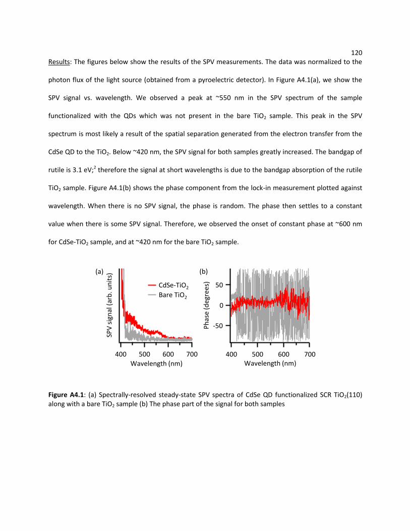
120 Results: The figures below show the results of the SPV measurements. The data was normalized to the
photon flux of the light source (obtained from a pyroelectric detector). In Figure A4.1(a), we show the
SPV signal vs. wavelength. We observed a peak at ~550 nm in the SPV spectrum of the sample
functionalized with the QDs which was not present in the bare TiO2 sample. This peak in the SPV
spectrum is most likely a result of the spatial separation generated from the electron transfer from the
CdSe QD to the TiO2. Below ~420 nm, the SPV signal for both samples greatly increased. The bandgap of
rutile is 3.1 eV;2 therefore the signal at short wavelengths is due to the bandgap absorption of the rutile
TiO2 sample. Figure A4.1(b) shows the phase component from the lock-in measurement plotted against
wavelength. When there is no SPV signal, the phase is random. The phase then settles to a constant
value when there is some SPV signal. Therefore, we observed the onset of constant phase at ~600 nm
for CdSe-TiO2 sample, and at ~420 nm for the bare TiO2 sample.
Figure A4.1: (a) Spectrally-resolved steady-state SPV spectra of CdSe QD functionalized SCR TiO2(110) along with a bare TiO2 sample (b) The phase part of the signal for both samples
-50
0
50
Ph
ase
(deg
rees
)
700600500400Wavelength (nm)
SPV
sig
nal
(ar
b. u
nit
s)
700600500400
Wavelength (nm)
CdSe-TiO2
Bare TiO2
(a) (b)
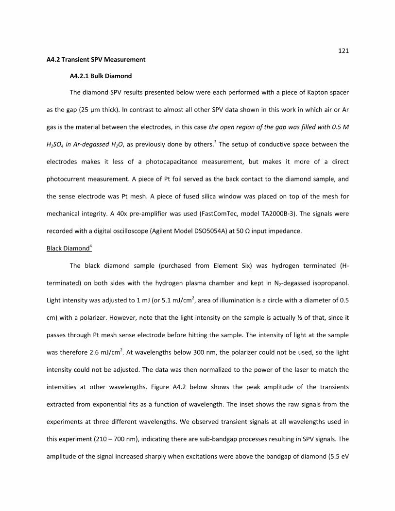
121 A4.2 Transient SPV Measurement
A4.2.1 Bulk Diamond
The diamond SPV results presented below were each performed with a piece of Kapton spacer
as the gap (25 μm thick). In contrast to almost all other SPV data shown in this work in which air or Ar
gas is the material between the electrodes, in this case the open region of the gap was filled with 0.5 M
H2SO4 in Ar-degassed H2O, as previously done by others.3 The setup of conductive space between the
electrodes makes it less of a photocapacitance measurement, but makes it more of a direct
photocurrent measurement. A piece of Pt foil served as the back contact to the diamond sample, and
the sense electrode was Pt mesh. A piece of fused silica window was placed on top of the mesh for
mechanical integrity. A 40x pre-amplifier was used (FastComTec, model TA2000B-3). The signals were
recorded with a digital oscilloscope (Agilent Model DSO5054A) at 50 Ω input impedance.
Black Diamond4
The black diamond sample (purchased from Element Six) was hydrogen terminated (H-
terminated) on both sides with the hydrogen plasma chamber and kept in N2-degassed isopropanol.
Light intensity was adjusted to 1 mJ (or 5.1 mJ/cm2, area of illumination is a circle with a diameter of 0.5
cm) with a polarizer. However, note that the light intensity on the sample is actually ½ of that, since it
passes through Pt mesh sense electrode before hitting the sample. The intensity of light at the sample
was therefore 2.6 mJ/cm2. At wavelengths below 300 nm, the polarizer could not be used, so the light
intensity could not be adjusted. The data was then normalized to the power of the laser to match the
intensities at other wavelengths. Figure A4.2 below shows the peak amplitude of the transients
extracted from exponential fits as a function of wavelength. The inset shows the raw signals from the
experiments at three different wavelengths. We observed transient signals at all wavelengths used in
this experiment (210 – 700 nm), indicating there are sub-bandgap processes resulting in SPV signals. The
amplitude of the signal increased sharply when excitations were above the bandgap of diamond (5.5 eV
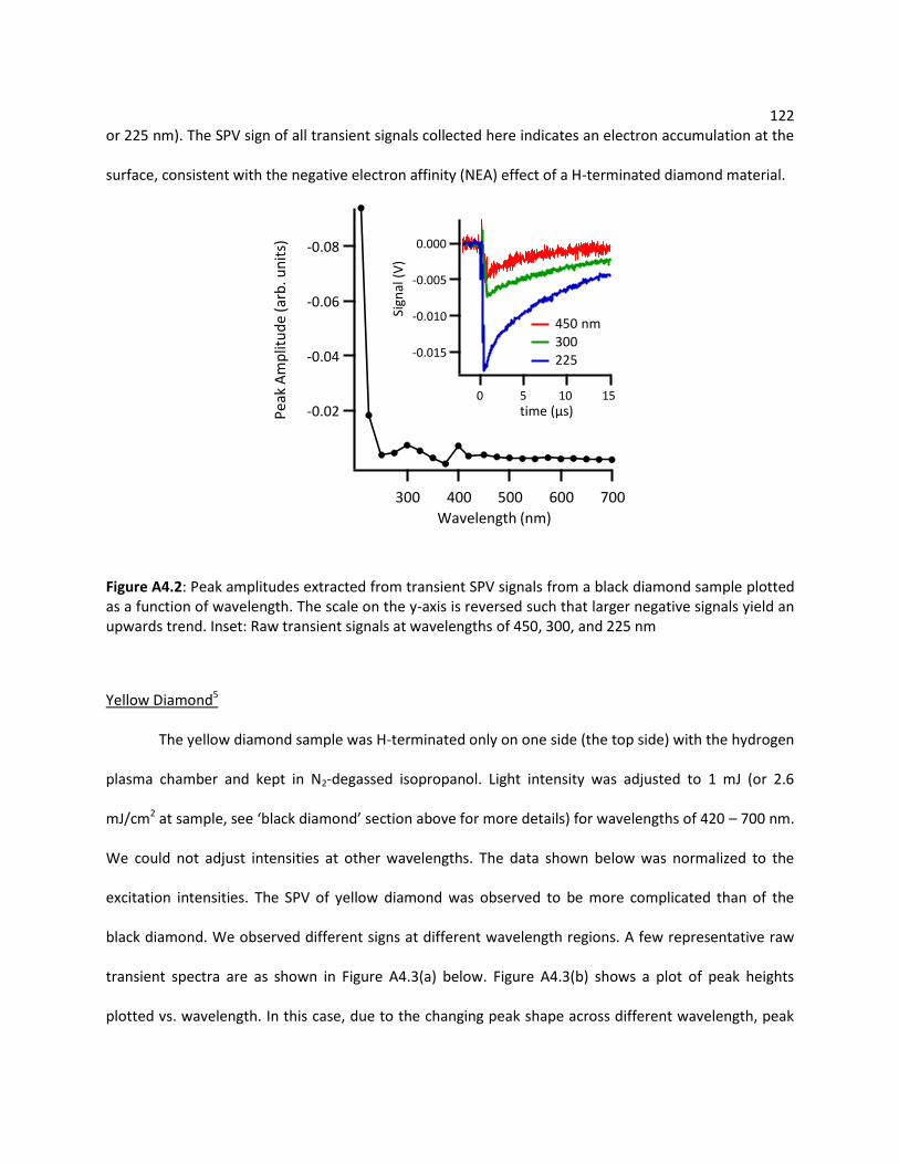
122 or 225 nm). The SPV sign of all transient signals collected here indicates an electron accumulation at the
surface, consistent with the negative electron affinity (NEA) effect of a H-terminated diamond material.
Figure A4.2: Peak amplitudes extracted from transient SPV signals from a black diamond sample plotted as a function of wavelength. The scale on the y-axis is reversed such that larger negative signals yield an upwards trend. Inset: Raw transient signals at wavelengths of 450, 300, and 225 nm
Yellow Diamond5
The yellow diamond sample was H-terminated only on one side (the top side) with the hydrogen
plasma chamber and kept in N2-degassed isopropanol. Light intensity was adjusted to 1 mJ (or 2.6
mJ/cm2 at sample, see ‘black diamond’ section above for more details) for wavelengths of 420 – 700 nm.
We could not adjust intensities at other wavelengths. The data shown below was normalized to the
excitation intensities. The SPV of yellow diamond was observed to be more complicated than of the
black diamond. We observed different signs at different wavelength regions. A few representative raw
transient spectra are as shown in Figure A4.3(a) below. Figure A4.3(b) shows a plot of peak heights
plotted vs. wavelength. In this case, due to the changing peak shape across different wavelength, peak
-0.08
-0.06
-0.04
-0.02Pea
k A
mp
litu
de
(arb
. un
its)
700600500400300
Wavelength (nm)
-0.015
-0.010
-0.005
0.000
Sign
al (
V)
151050time (μs)
450 nm300225
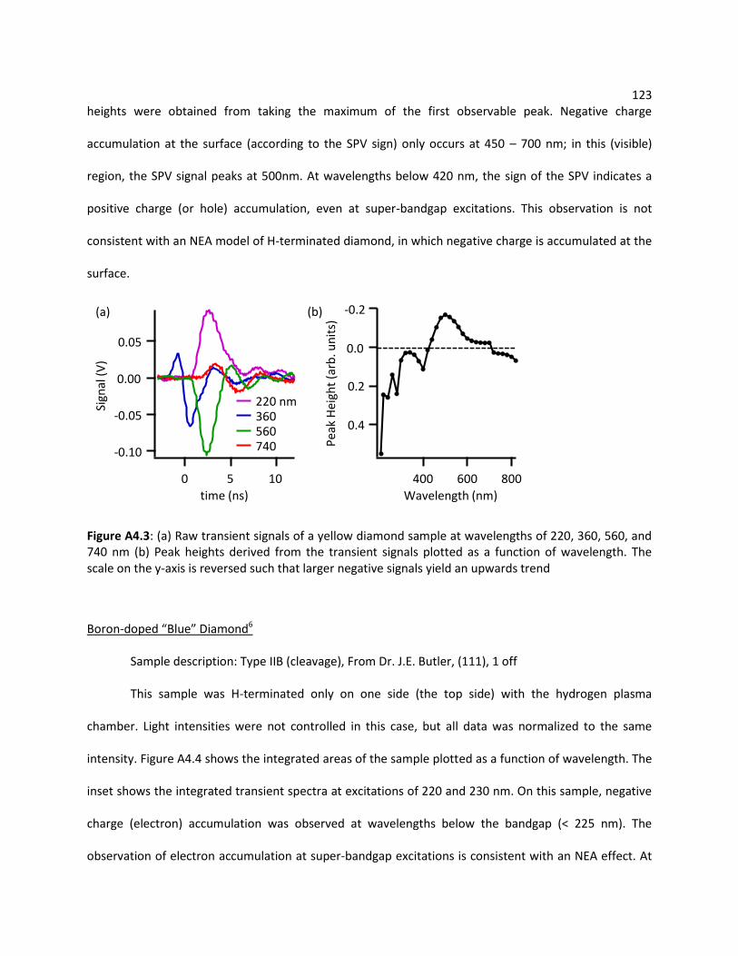
123 heights were obtained from taking the maximum of the first observable peak. Negative charge
accumulation at the surface (according to the SPV sign) only occurs at 450 – 700 nm; in this (visible)
region, the SPV signal peaks at 500nm. At wavelengths below 420 nm, the sign of the SPV indicates a
positive charge (or hole) accumulation, even at super-bandgap excitations. This observation is not
consistent with an NEA model of H-terminated diamond, in which negative charge is accumulated at the
surface.
Figure A4.3: (a) Raw transient signals of a yellow diamond sample at wavelengths of 220, 360, 560, and 740 nm (b) Peak heights derived from the transient signals plotted as a function of wavelength. The scale on the y-axis is reversed such that larger negative signals yield an upwards trend
Boron-doped “Blue” Diamond6
Sample description: Type IIB (cleavage), From Dr. J.E. Butler, (111), 1 off
This sample was H-terminated only on one side (the top side) with the hydrogen plasma
chamber. Light intensities were not controlled in this case, but all data was normalized to the same
intensity. Figure A4.4 shows the integrated areas of the sample plotted as a function of wavelength. The
inset shows the integrated transient spectra at excitations of 220 and 230 nm. On this sample, negative
charge (electron) accumulation was observed at wavelengths below the bandgap (< 225 nm). The
observation of electron accumulation at super-bandgap excitations is consistent with an NEA effect. At
-0.10
-0.05
0.00
0.05
Sign
al (
V)
1050
time (ns)
220 nm360560740
0.4
0.2
0.0
-0.2
Pea
k H
eigh
t (a
rb. u
nit
s)
800600400
Wavelength (nm)
(a) (b)

124 wavelengths > 225 nm, we observed small signals with the opposite sign, indicating some sub-bandgap
processes leading to SPV, with hole accumulation at the surface.
-1000
-500
0
Inte
grat
ed A
rea
(arb
. un
its)
320280240
Wavelength (nm)
-80
-40
0
Inte
grat
ed S
ign
al
3020100Time (ns)
220 nm230
Figure A4.4: Peak areas extracted from transient SPV signals plotted as a function of wavelength of a boron-doped diamond sample. The scale on the y-axis is reversed such that larger negative signals yield an upwards trend. Inset: Integrated transient signals at wavelengths of 220 and 230 nm

125 A4.2.2 N719 Dye on Porous Nanocrystalline TiO2 Films7
Sample Preparation: Porous TiO2 nanocrystalline thin film was screen-printed onto fluorine-doped thin
oxide (FTO) coated glass and annealed as described in Chapter 2 of the thesis. The film was then
additionally cleaned at 500 C for 15 min to remove any adsorbed water and organic contaminants. A
saturated solution of N719 dye (Solaronix) was made in a mixture of anhydrous acetonitrile (ACN) and
anhydrous tert-butanol (50:50 by volume). The solution was kept in the dark. The clean TiO2 film was
immersed in the N719 dye solution (while the film was still warm to the touch) and left in the dark
overnight. After dye adsorption, the film was rinsed with anhydrous ACN.
SPV Measurement Setup: The sample was sandwiched with a Kapton spacer (25 μm thick) and another
piece of FTO glass into an SPV cell. The open region as defined by the Kapton spacer was filled with air.
The 40x preamplifier and Faraday cage were used. Optical excitation from the ns-laser was set to 500
nm and the intensity was adjusted with a polarizer to be 50 μJ ( 128 μJ/cm2 at sample, after accounting
for Faraday cage and a laser beam of ~0.5 cm in diameter).
Results: Figure A4.5 shows the transient signal of the dyed TiO2 sample. The positive signal indicates
electron transfer from the N719 dye into the TiO2 film, therefore leaving positive charges on the surface.
Sign
al (
arb
. un
its)
150100500Time (ns)
Figure A4.5: Transient SPV signal at 500 nm of a sample of a nanocrystalline TiO2 film dyed with N719
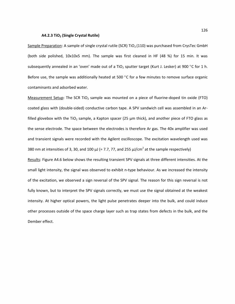
126 A4.2.3 TiO2 (Single Crystal Rutile)
Sample Preparation: A sample of single crystal rutile (SCR) TiO2 (110) was purchased from CrysTec GmbH
(both side polished, 10x10x5 mm). The sample was first cleaned in HF (48 %) for 15 min. It was
subsequently annealed in an ‘oven’ made out of a TiO2 sputter target (Kurt J. Lesker) at 900 C for 1 h.
Before use, the sample was additionally heated at 500 C for a few minutes to remove surface organic
contaminants and adsorbed water.
Measurement Setup: The SCR TiO2 sample was mounted on a piece of fluorine-doped tin oxide (FTO)
coated glass with (double-sided) conductive carbon tape. A SPV sandwich cell was assembled in an Ar-
filled glovebox with the TiO2 sample, a Kapton spacer (25 μm thick), and another piece of FTO glass as
the sense electrode. The space between the electrodes is therefore Ar gas. The 40x amplifier was used
and transient signals were recorded with the Agilent oscilloscope. The excitation wavelength used was
380 nm at intensities of 3, 30, and 100 μJ ( 7.7, 77, and 255 μJ/cm2 at the sample respectively)
Results: Figure A4.6 below shows the resulting transient SPV signals at three different intensities. At the
small light intensity, the signal was observed to exhibit n-type behaviour. As we increased the intensity
of the excitation, we observed a sign reversal of the SPV signal. The reason for this sign reversal is not
fully known, but to interpret the SPV signals correctly, we must use the signal obtained at the weakest
intensity. At higher optical powers, the light pulse penetrates deeper into the bulk, and could induce
other processes outside of the space charge layer such as trap states from defects in the bulk, and the
Dember effect.

127
Figure A4.6: Transient SPV signal at 380 nm of a single crystal rutile TiO2 (110) sample at three different intensities
Sign
al (
arb
.un
its)
3020100
Time (ns)
3 μJ30100
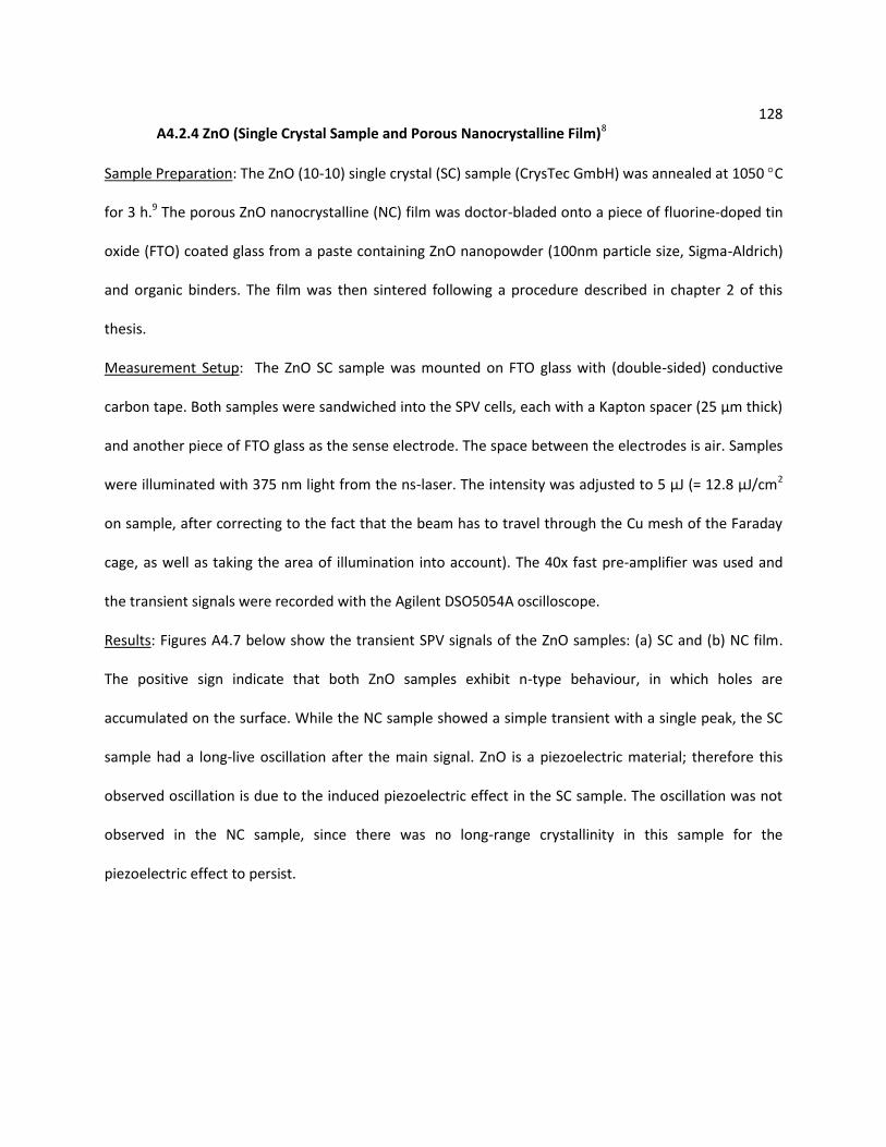
128 A4.2.4 ZnO (Single Crystal Sample and Porous Nanocrystalline Film)8
Sample Preparation: The ZnO (10-10) single crystal (SC) sample (CrysTec GmbH) was annealed at 1050 C
for 3 h.9 The porous ZnO nanocrystalline (NC) film was doctor-bladed onto a piece of fluorine-doped tin
oxide (FTO) coated glass from a paste containing ZnO nanopowder (100nm particle size, Sigma-Aldrich)
and organic binders. The film was then sintered following a procedure described in chapter 2 of this
thesis.
Measurement Setup: The ZnO SC sample was mounted on FTO glass with (double-sided) conductive
carbon tape. Both samples were sandwiched into the SPV cells, each with a Kapton spacer (25 μm thick)
and another piece of FTO glass as the sense electrode. The space between the electrodes is air. Samples
were illuminated with 375 nm light from the ns-laser. The intensity was adjusted to 5 μJ ( 12.8 μJ/cm2
on sample, after correcting to the fact that the beam has to travel through the Cu mesh of the Faraday
cage, as well as taking the area of illumination into account). The 40x fast pre-amplifier was used and
the transient signals were recorded with the Agilent DSO5054A oscilloscope.
Results: Figures A4.7 below show the transient SPV signals of the ZnO samples: (a) SC and (b) NC film.
The positive sign indicate that both ZnO samples exhibit n-type behaviour, in which holes are
accumulated on the surface. While the NC sample showed a simple transient with a single peak, the SC
sample had a long-live oscillation after the main signal. ZnO is a piezoelectric material; therefore this
observed oscillation is due to the induced piezoelectric effect in the SC sample. The oscillation was not
observed in the NC sample, since there was no long-range crystallinity in this sample for the
piezoelectric effect to persist.

129
Figure A4.7: Transient SPV signal at 375 nm of ZnO: (a) single crystal and (b) nanocrystalline thin film
806040200-20
Time (ns)
806040200-20
Time (ns)
Sign
al (
arb
. un
its)
(a) (b)
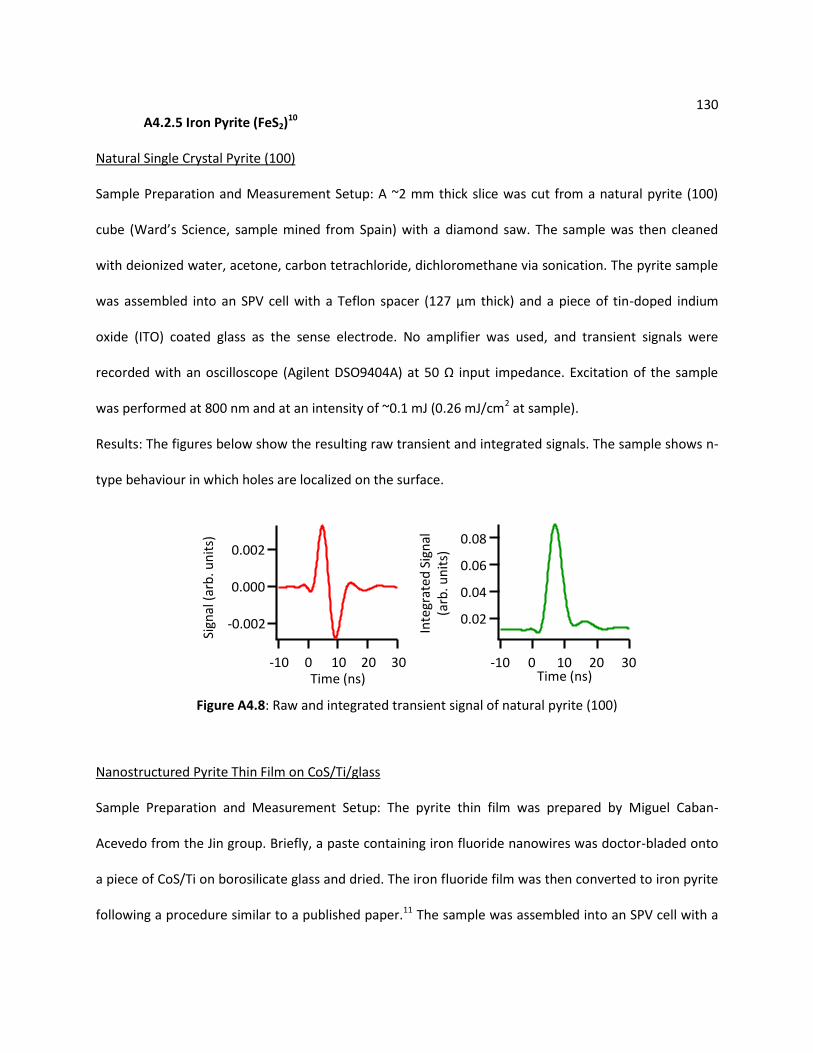
130 A4.2.5 Iron Pyrite (FeS2)
10
Natural Single Crystal Pyrite (100)
Sample Preparation and Measurement Setup: A ~2 mm thick slice was cut from a natural pyrite (100)
cube (Ward’s Science, sample mined from Spain) with a diamond saw. The sample was then cleaned
with deionized water, acetone, carbon tetrachloride, dichloromethane via sonication. The pyrite sample
was assembled into an SPV cell with a Teflon spacer (127 μm thick) and a piece of tin-doped indium
oxide (ITO) coated glass as the sense electrode. No amplifier was used, and transient signals were
recorded with an oscilloscope (Agilent DSO9404A) at 50 Ω input impedance. Excitation of the sample
was performed at 800 nm and at an intensity of ~0.1 mJ (0.26 mJ/cm2 at sample).
Results: The figures below show the resulting raw transient and integrated signals. The sample shows n-
type behaviour in which holes are localized on the surface.
Figure A4.8: Raw and integrated transient signal of natural pyrite (100)
Nanostructured Pyrite Thin Film on CoS/Ti/glass
Sample Preparation and Measurement Setup: The pyrite thin film was prepared by Miguel Caban-
Acevedo from the Jin group. Briefly, a paste containing iron fluoride nanowires was doctor-bladed onto
a piece of CoS/Ti on borosilicate glass and dried. The iron fluoride film was then converted to iron pyrite
following a procedure similar to a published paper.11 The sample was assembled into an SPV cell with a
Sign
al (
arb
. un
its)
Inte
grat
ed S
ign
al
(arb
. un
its)0.002
0.000
-0.002
3020100-10Time (ns)
0.08
0.06
0.04
0.02
3020100-10Time (ns)
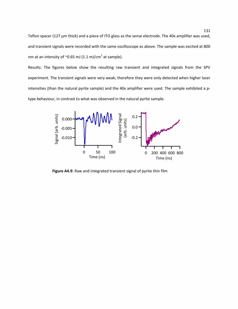
131 Teflon spacer (127 μm thick) and a piece of ITO glass as the sense electrode. The 40x amplifier was used,
and transient signals were recorded with the same oscilloscope as above. The sample was excited at 800
nm at an intensity of ~0.65 mJ (1.1 mJ/cm2 at sample).
Results: The figures below show the resulting raw transient and integrated signals from the SPV
experiment. The transient signals were very weak; therefore they were only detected when higher laser
intensities (than the natural pyrite sample) and the 40x amplifier were used. The sample exhibited a p-
type behaviour, in contrast to what was observed in the natural pyrite sample.
Sign
al (
arb
. un
its)
Inte
grat
ed S
ign
al
(arb
. un
its)
-0.010
-0.005
0.000
100500
-0.2
0.0
0.2
8006004002000Time (ns) Time (ns)
Figure A4.9: Raw and integrated transient signal of pyrite thin film

132 A4.2.6 Layered Chalcogenide Nanostructures of MoS2, WS2, and WSe2
12
Measurement Setup: The nanostructured samples were synthesized by Mark Lukowski (Jin group) on
two substrates: Al foil or fluorine-doped tin oxide (FTO) coated glass. They were each sandwiched into
an SPV cell with a spacer and a piece of FTO glass as the sense electrode. Optical excitation of the
sample was set to 700 nm with the ns-laser, at intensities of approximately 1 mJ (= 2.6 mJ/cm2 at
sample; area of beam = 0.196 cm2, and the beam also passed through the Cu mesh of the Faraday cage)
The 40x amplifier was used, and the transient signals were recorded with an oscilloscope (Agilent
DSO9404A) at 50 Ω input impedance. All samples exhibited p-type behaviour.
Figure A4.10: Integrated transient signals of nanostructured (a) MoS2 (b) WS2 (c) WSe2 on FTO glass, and (d) WSe2 on Al foil
-0.4
-0.2
0.0
6040200-20
Time (ns)
-20
-10
0
3210-1
Time (μs)
-0.10
-0.05
0.00
2000
Time (ns)
-0.8
-0.6
-0.4
-0.2
0.0
2000
Time (ns)
Inte
grat
ed S
ign
al(a
rb.u
nit
s)In
tegr
ated
Sig
nal
(arb
.un
its)
MoS2
WS2
WSe2/FTO
WSe2/Al
(a) (b)
(c) (d)

133 A4.2.7 Sensitized SnO2
Ru-polypyridyl complex sensitized SnO2 nanoparticle film13
This SPV data is as published in ACS Appl. Mater. Interfaces, 2011, 3, 3110–3119
Figure A4.11: Raw transient SPV signals of (a) bare SnO2 film and (b) Ru-complex sensitized SnO2 (c) The amplitude extracted from the transient SPV signals of the sensitized film plotted against excitation wavelength
(a) (b)
(c)
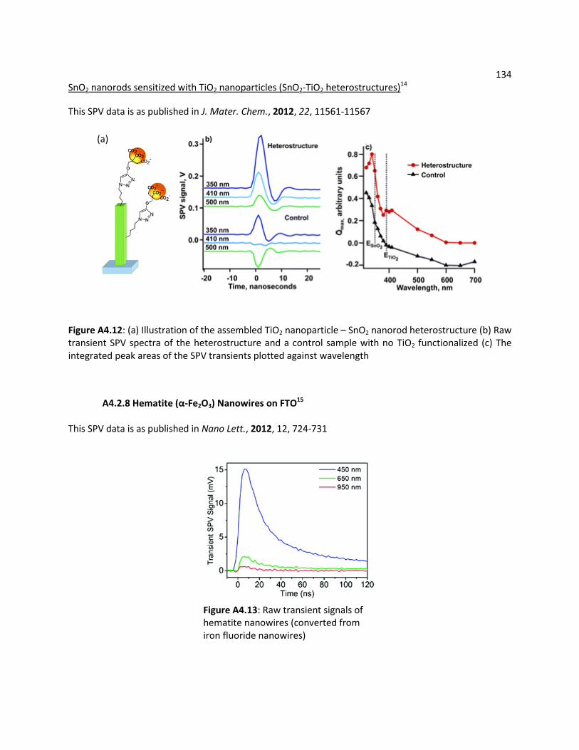
134 SnO2 nanorods sensitized with TiO2 nanoparticles (SnO2-TiO2 heterostructures)14
This SPV data is as published in J. Mater. Chem., 2012, 22, 11561-11567
Figure A4.12: (a) Illustration of the assembled TiO2 nanoparticle – SnO2 nanorod heterostructure (b) Raw transient SPV spectra of the heterostructure and a control sample with no TiO2 functionalized (c) The integrated peak areas of the SPV transients plotted against wavelength
A4.2.8 Hematite (α-Fe2O3) Nanowires on FTO15
This SPV data is as published in Nano Lett., 2012, 12, 724-731
(a)
Figure A4.13: Raw transient signals of hematite nanowires (converted from iron fluoride nanowires)

135 A4.3 Ultrafast SPV
Please refer to Chapter 5, section 5.4 for a more complete explanation of the scientific background and
experimental setup.
A4.3.1 Ultrafast SPV of n-GaAs
Sample description: Si-doped (n-type) single crystal wafer of GaAs(100) was purchased from MTI Corp.
From the specification sheet, the sample has a carrier concentration of (1.0 - 1.8) x 1018 cm-3.
Measurement Setup: The sample (with a Zr foil as the back contact) was sandwiched into an SPV cell
with a Teflon spacer (127 μm thick) and a piece of tin-doped indium oxide (ITO) coated glass (30 – 60
Ω/sq, Sigma-Aldrich product 703184) as the sense electrode. The sample was first verified to exhibit
spatial charge separation characteristic of an n-type semiconductor (holes are localized on surface) by
the sign of the transient signal as recorded on the oscilloscope. For the ultrafast delay scan, the sense
electrode was connected to ground so that we obtain a negative transient signal. The transient signal is
shown in Figure A4.14(a).16 This was done because the diode operated in the negative bias
configuration. The sample was illuminated through the sense electrode from a Ti:sapphire regenerative
amplifier (Spitfire Pro, Spectra-Physics) with a central wavelength of 800 nm at 1 kHz repetition rate. The
pulses were split into two to perform a delay scan and were adjusted to 3.0 and 3.4 mW (= 15 and 17
mW/cm2 respectively, the size of the beam was approximately 0.5 cm in diameter) with a neutral
density filter, as measured by a Si-detector (Thorlabs S120VC Si-photodiode detector). The signal was
then pre-amplified (100x amplification, from two 10x Fast ComTec Model TA2000B-1 connected in
series) before going through a fast diode (Model 203A from Krytar, 10 MHz – 20 GHz zero bias Schottky
detector operating at negative polarity) and recorded with a boxcar averager (Stanford Research
Systems Model SR250). Figure A4.14(b) shows the transient signal after the diode, and the gate width of
the boxcar averager.16
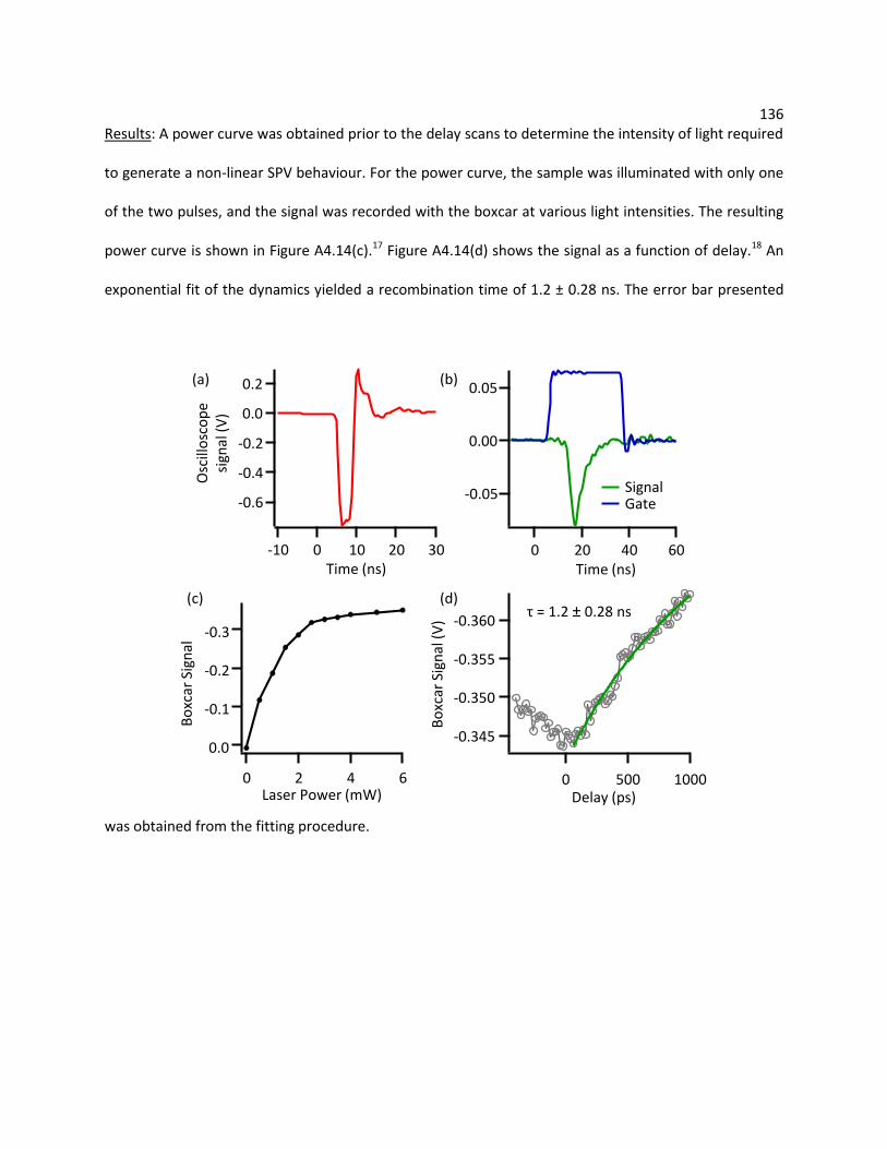
136 Results: A power curve was obtained prior to the delay scans to determine the intensity of light required
to generate a non-linear SPV behaviour. For the power curve, the sample was illuminated with only one
of the two pulses, and the signal was recorded with the boxcar at various light intensities. The resulting
power curve is shown in Figure A4.14(c).17 Figure A4.14(d) shows the signal as a function of delay.18 An
exponential fit of the dynamics yielded a recombination time of 1.2 ± 0.28 ns. The error bar presented
was obtained from the fitting procedure.
-0.3
-0.2
-0.1
0.0
Bo
xcar
Sig
nal
6420Laser Power (mW)
-0.360
-0.355
-0.350
-0.345
10005000
τ = 1.2 0.28 ns
Delay (ps)
Bo
xcar
Sig
nal
(V
)
-0.05
0.00
0.05
6040200
SignalGate
Time (ns)
-0.6
-0.4
-0.2
0.0
0.2
3020100-10Time (ns)
Osc
illo
sco
pe
sign
al (
V)
(a) (b)
(c) (d)
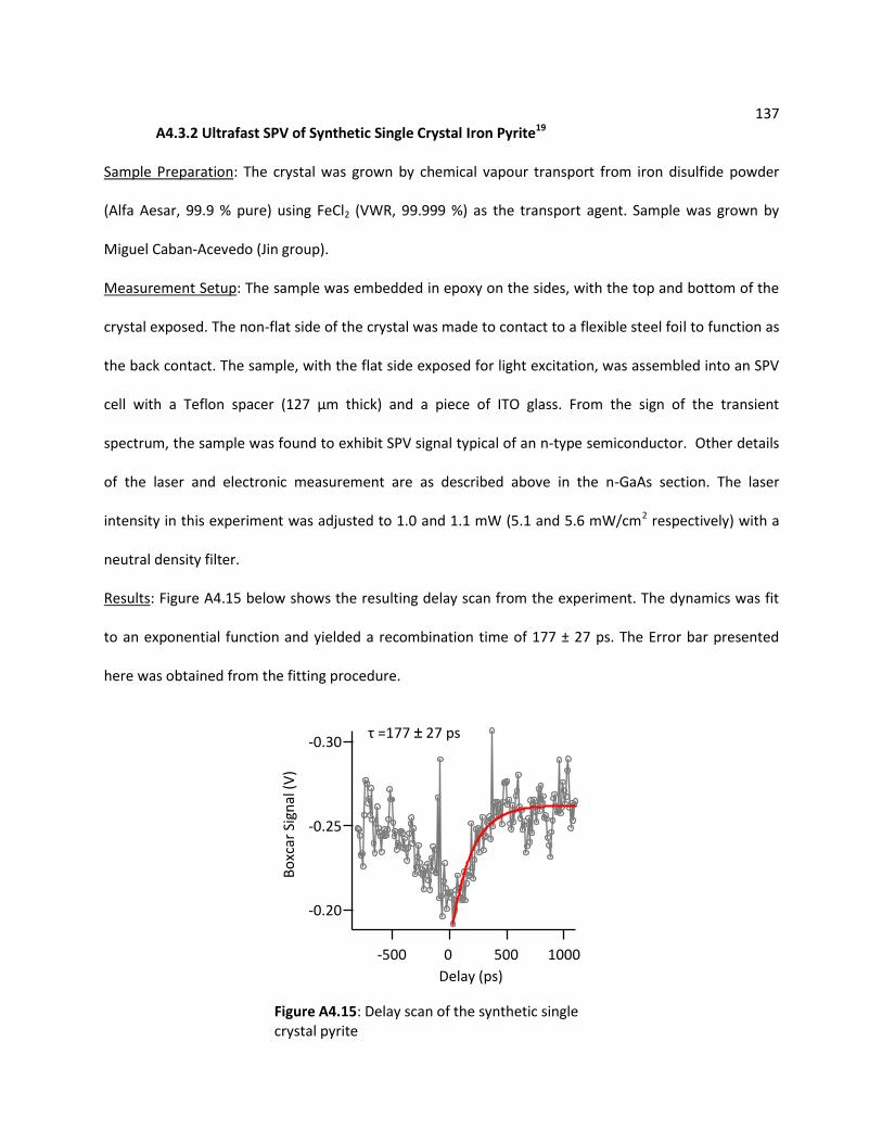
137 A4.3.2 Ultrafast SPV of Synthetic Single Crystal Iron Pyrite19
Sample Preparation: The crystal was grown by chemical vapour transport from iron disulfide powder
(Alfa Aesar, 99.9 % pure) using FeCl2 (VWR, 99.999 %) as the transport agent. Sample was grown by
Miguel Caban-Acevedo (Jin group).
Measurement Setup: The sample was embedded in epoxy on the sides, with the top and bottom of the
crystal exposed. The non-flat side of the crystal was made to contact to a flexible steel foil to function as
the back contact. The sample, with the flat side exposed for light excitation, was assembled into an SPV
cell with a Teflon spacer (127 μm thick) and a piece of ITO glass. From the sign of the transient
spectrum, the sample was found to exhibit SPV signal typical of an n-type semiconductor. Other details
of the laser and electronic measurement are as described above in the n-GaAs section. The laser
intensity in this experiment was adjusted to 1.0 and 1.1 mW (5.1 and 5.6 mW/cm2 respectively) with a
neutral density filter.
Results: Figure A4.15 below shows the resulting delay scan from the experiment. The dynamics was fit
to an exponential function and yielded a recombination time of 177 ± 27 ps. The Error bar presented
here was obtained from the fitting procedure.
-0.30
-0.25
-0.20
10005000-500
τ =177 27 ps
Delay (ps)
Bo
xcar
Sig
nal
(V
)
Figure A4.15: Delay scan of the synthetic single crystal pyrite
138 A4.4 References
1. Notebook Entry: YU049, SPV of CdSe/OA on SCR110dTiO2/MPA with Cu Back Contact in Cell
2. Linsebigler, A. L.; Lu, G.; Yates, J. T. Photocatalysis on TiO2 Surfaces: Principles, Mechanisms, and Selected Results, Chem. Rev. 1995, 95, 735-758.
3. Pleskov, Y. V. Photochemistry of Synthetic Diamond Electrodes. Diamond and Diamond-Like Film Applications; Technomic Publishing Company: Lancaster, Pennsylvania; 1996; pp 90-96.
4. Notebook Entry: YU090, Transient PV of Black Diamond (with faster amplifier)
5. Notebook Entry: YU103, Transient PV and UV-Vis of Yellow Diamond (w/ NIR wavelengths)
6. Notebook Entry: YU108, Photovoltage (Transient) of Boron-Doped Diamond
7. Notebook Entry: YU139, Transient SPV of N719 on TiO2nc, Varying Intensity
8. Notebook Entry: YU233, Transient SPV of nSi, ZnOsc w/ C tape, ZnOnc, Use of Slow Current Amp
9. Chen, J. X.; Ruther, R. E.; Tan, Y. Z.; Bishop, L. M.; Hamers, R. J. Molecular Adsorption on ZnO(10(1)over-bar0) Single-Crystal Surfaces: Morphology and Charge Transfer, Langmuir 2012, 28, 10437-10445.
10. Notebook Entry: YV205, Transient SPV of Natural Pyrite and Pyrite Thin Film
11. Faber, M. S.; Park, K.; Cabán-Acevedo, M.; Santra, P. K.; Jin, S. Earth-Abundant Cobalt Pyrite (CoS2) Thin Film on Glass as a Robust, High-Performance Counter Electrode for Quantum Dot-Sensitized Solar Cells, J. Phys. Chem. Lett 2013, 4, 1843–1849.
12. yizheng_archive3\For Jin Group\Mark\SPV for mark 082012
13. Benson, M. C.; Ruther, R. E.; Gerken, J. B.; Rigsby, M. L.; Bishop, L. M.; Tan, Y.; Stahl, S. S.; Hamers, R. J. Modular "Click" Chemistry for Electrochemically and Photoelectrochemically Active Molecular Interfaces to Tin Oxide Surfaces, ACS Appl. Mater. Interfaces 2011, 3, 3110-3119.
14. Shah, S.; Benson, M. C.; Bishop, L. M.; Huhn, A. M.; Ruther, R. E.; Yeager, J. C.; Tan, Y.; Louis, K. M.; Hamers, R. J. Chemically assembled heterojunctions of SnO2 nanorods with TiO2 nanoparticles via "click" chemistry, J. Mater. Chem. 2012, 22, 11561-11567.
15. Li, L.; Yu, Y.; Meng, F.; Tan, Y.; Hamers, R. J.; Jin, S. Facile Solution Synthesis of α-FeF3·3H2O Nanowires and Their Conversion to α-Fe2O3 Nanowires for Photoelectrochemical Application, Nano Lett. 2012, 12, 724-731.
16. Notebook Entry: YV212, Ultrafast SPV
17. Notebook Entry: YV191, Ultrafast SPV
18. Notebook Entry: YV198, Ultrafast SPV

139 19. Notebook Entry: YV185, Ultrafast SPV