Operation and Characterization from Electric Cool Ge ...
32
Operation and Characterization from Electric Cool Ge Detectors at KSNL Henry T. Wong (with Vivek Sharma) Institute of Physics, Academia Sinica, Taiwan @
Transcript of Operation and Characterization from Electric Cool Ge ...

Operation and Characterization from Electric Cool Ge Detectors at KSNL
Henry T. Wong (with Vivek Sharma)
Institute of Physics, Academia Sinica, Taiwan @

Outline of Talk
Overview Electro-cooled Ge Detectors. Operation & Problems Performance: Threshold and background. Sensitivity for Low energy physics Future Prospects
Design of ECGe
Top View Side View
Cooler Coldfinger Air InAir Out Pre-AmpDetector
Capsule
ControllerFront Panel
DisplayFront Panel
LEDs

Temperature and Power Profile
Thermal Recycle
Controller

Advantage of Electro-cool Ge detectors
Customize Coldtip temperature for best frontend performance
Cooling with synchronized negative feedback pumping.
Less microphonic noise.
Compact (Portable) Design.
New JFET and ASIC FE-electronics near point contact.

Timing Amp
Generation Mass(g)
Pulsar FWHM(eVee)
Threshold(eVee)
G1500 130 500
G2900 100 300
G3900 70 200
G3+1430 ~60 ~160
p- PCGe[500g – 1 kg]
p+
n+(~1mm Li diffused)
n- PCGe[500 g]
n+
p+(~0.5 μm Boron implanted)500 g
900 g
Pulsar FWHM and Threshold
Liquid Nitrogen
Electro-cool

Operation Problems (Difficulties)
Electro-cooler not powerful enough to cool down after some months -- due to outgassing of internal components.Solution: Necessary to do regular pump down by
an external pump to remove residual air.Most performing front-end electronics have:
higher background (not yet low-background compatible)
High failure rates Repairs & Upgrades take long time than “regular”
devices, indicating learning curve from company as well …..

G3+ Generation Detector ..
Germanium detector at -185 CThreshold secured 200 eVPulsar FWHM 70 eVClean Surface Bulk band
Stable dataStable dataUnstable data
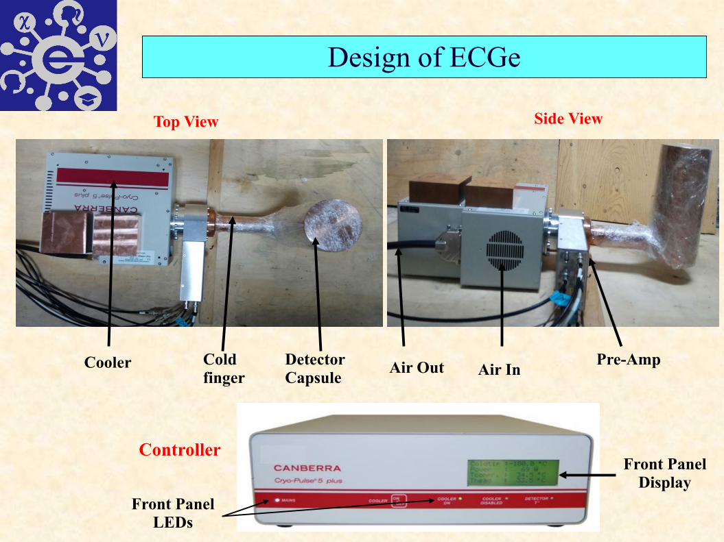
G3 Generation Detector
Data collected with G3 detector:30 kgd (-190 C)
Encountered problems:200 eV threshold.Pulsar FWHM 70 eV.Controlled background.

Status to probe νAel
Differential νAel
G2 (Achieved)G3 (Achieved)
G3+ (Target)

THU Ge-activities
Litao Yang (THU)
On behalf of CDEX
1The 3rd PIRE-GEMADARC Collaboration Meeting, Dec. 5th, 2018, Knoxville

2
The manufacture of HPGe
Mechanical Preparation Lithium Diffusion Wet Lab
Boron Ion Implant Surface Passivation
HPGe detector
Vacuum Coating Machine

束流
束流
束流
束流
自转工件光栏
3
New Ion Implanter
束流方向
工件光栏
束流方向
0-90.0°
自转
上下运动
光栏工件
Specially designed for HPGe injection, Max. crystal size: Φ100mmX90mm
Injection elements: B, P, Ar
diaphragmcrystal
beam
4
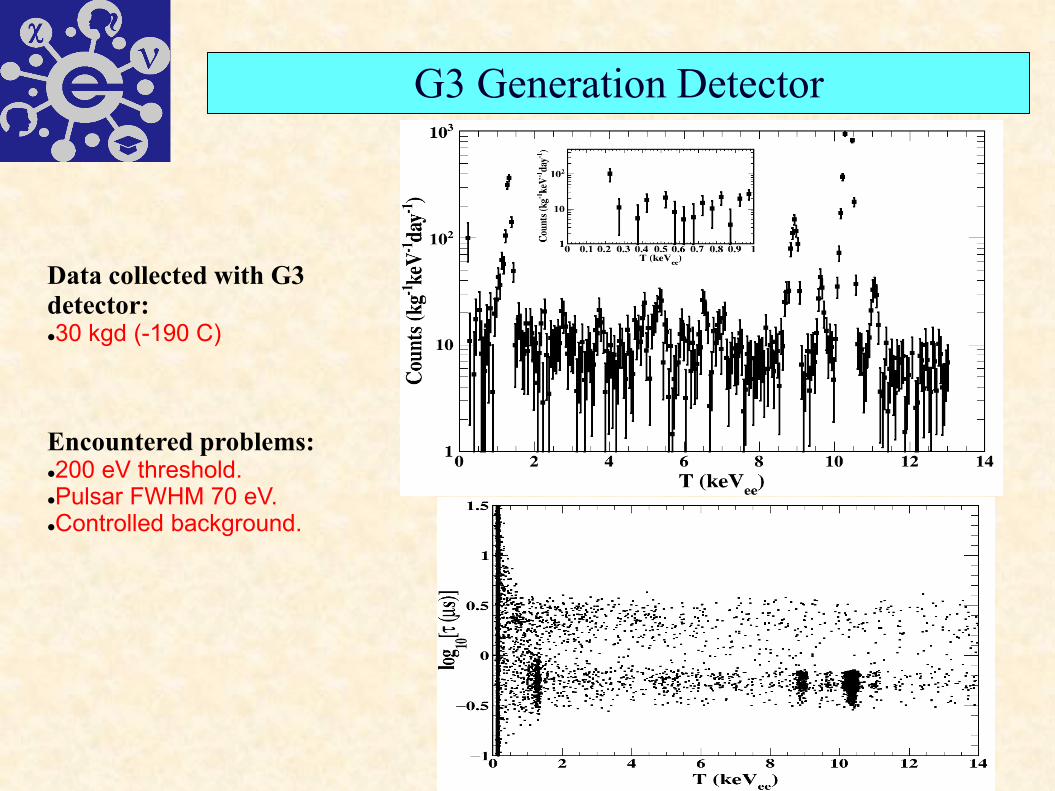
Laboratory and equipment upgrades
Glove box @ CJPL-I Fume hood
Water Purifier
Glove box @ THU
First assembly test of the home-made HPGe
detector in CJPL-I was completed;
A small LN2 tank was equipped in the glove
box@THU, for the test of Bare HPGe in LN2;

5
Long-term stability study
Detector: 19#
PPCGe detector, Φ50mm X 50mm
Pre-amplifier: Pulse-reset
Latest measure results(2018/10/24):
Leakage current: 16pA
FWHM: 0.72keV@122keV, [email protected] at room temperature, cooled down for
test, good performance keeping, >1300 days
6
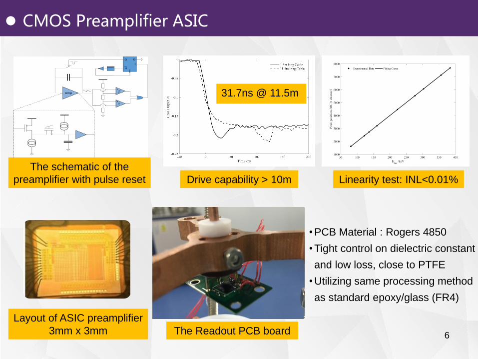
CMOS Preamplifier ASIC
31.7ns @ 11.5m
The schematic of the
preamplifier with pulse reset
Layout of ASIC preamplifier
3mm x 3mm
Drive capability > 10m Linearity test: INL<0.01%
• PCB Material : Rogers 4850
• Tight control on dielectric constant
and low loss, close to PTFE
• Utilizing same processing method
as standard epoxy/glass (FR4)
The Readout PCB board

7
THU-1: ASIC + PPCGe
First 500g home-made PPCGe+ASIC finished testing, energy
resolution and energy threshold compared with commercial one.
Low noise & low bkg ASIC electronics
PPC: 50mm x 50mm
8
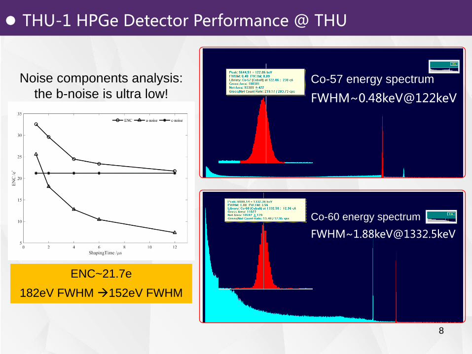
THU-1 HPGe Detector Performance @ THU
Co-57 energy spectrum
FWHM~0.48keV@122keV
Co-60 energy spectrum
ENC~21.7e
182eV FWHM 152eV FWHM
Noise components analysis:
the b-noise is ultra low!

9
THU-1 HPGe Detector Performance @ CJPL
Reset Period ~ 5.7s, Leakage Current ~ 0.043pA.
Background spectrum
@high energy region (0~3000keV)
Background spectrum
@low energy region (0~20keV)
201712 T1 (3.15d)
201809 T1 (8.83d)
201712 T1 (3.15d)
201809 T1 (8.83d)
threshold ~300eV
Ge-68 KX
Commercial Ge crystal;
Structure machining;
Li-drift and B-implanted;
Home-made ULB PreAmp;
Underground EF-Cu;
Underground assemble;
Underground testing…

10
Bare HPGe detectors in LN2
• Vacuum chamber, structure materials, not conducive to
further reduce the radioactive background;
• ASIC-based preamplifiers can work well in liquid nitrogen;
Develop bare HPGe detectors immersed into LN2!
CDEX-10 detector string layout

11
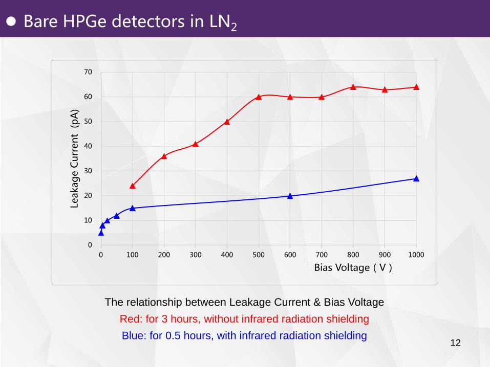
Bare HPGe detectors in LN2
• The leakage current was measured by an electrometer, which also
supplied the high voltage at the same time;
• In order to shield infrared radiation, we used a similar design from Gerda.
A copper sheet is placed above the crystal holder to block infrared
radiation from the LN2 tank, lower the leakage current.
Detector structure of testBare HPGe detectors
(with infrared radiation shielding)
Electrometer
/high resistance meter
12
Bare HPGe detectors in LN2
0
10
20
30
40
50
60
70
0 100 200 300 400 500 600 700 800 900 1000
Leakag
e C
urr
en
t (
pA
)
Bias Voltage(V)
The relationship between Leakage Current & Bias Voltage
Red: for 3 hours, without infrared radiation shielding
Blue: for 0.5 hours, with infrared radiation shielding

13
0
5
10
15
20
25
30
0 1 2 3 4 5 6 7 8
Leakag
e C
urr
en
t(p
A)
Time(h)
The relationship between Leakage Current & Time
(1000V, with infrared radiation shielding )
Immerse the detector into liquid
nitrogen for about 8 hours, we got
a stable leakage current ~10 pA
for 1000V bias voltage.
Bare HPGe detectors in LN2
PPC: 50mm x 50mm
Depleted voltage: ~800V
Bare HPGe in LN2

14
Low background VFE
• Flexible Cable
– lower background than coaxial cable
– now: Kapton
– next plan: PTFE (more pure, longer)
• Si substrate
– The lowest background circuit
substrate material
– Micromachining low mass
– The first version of silicon substrate
processing is currently completed
The ASIC board with 60cm long Flexible cable
The performances of ASIC Preamplifier
with Flexible cable are not degraded.
-noise --risetime Wiring
(After plating)
Central through-hole
(After plating)
Silicon substrate designSilicon substrate
processing

surface events discarded
Bulk
EFEs
15
EFEs in CDEX-1B/10 background data
Bulk
EFEs
Bulk + EFEs
Measured pulses:
Top: Bulk event
Bottom: EFE
raw pulse
risetime fitting

16
Detector simulation
Electric field Weighting potential
• P-type Point-Contact (PPCGe) detector:
Small point-like central contact
Especially low capacitance (~ 1pF) gives superb
energy resolution and low energy threshold
• Pulses generated by
Geant4: interaction & energy deposition;
ICC package: Induced Charge/Current signal
(Shockley-Ramo theorem);
Finite element analysis
of E-field (Maxwell)
Impurity concentration:
[-0.5,-0.8]×1010cm-3
no radial gradient
Bias Voltage:
+ 3000V

17
EFEs origin -- detector simulation
Drift time contour
• The very-bulk events mainly arise from the
bottom part of the PPC detector
• Very-bulk events discrimination can
probably be used for background rejection
Drift time distribution
18
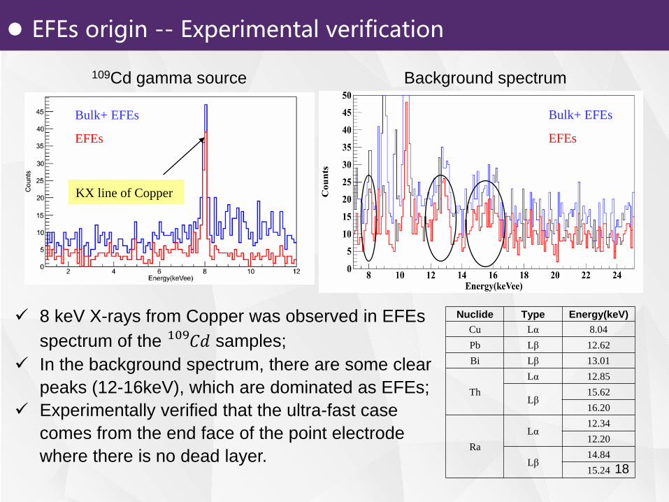
EFEs origin -- Experimental verification
Bulk+ EFEs
EFEs
109Cd gamma source
KX line of Copper
Nuclide Type Energy(keV)
Cu Lα 8.04
Pb Lβ 12.62
Bi Lβ 13.01
Th
Lα 12.85
Lβ15.62
16.20
Ra
Lα12.34
12.20
Lβ14.84
15.24
Background spectrum
Bulk+ EFEs
EFEs
8 keV X-rays from Copper was observed in EFEs
spectrum of the 109𝐶𝑑 samples;
In the background spectrum, there are some clear
peaks (12-16keV), which are dominated as EFEs;
Experimentally verified that the ultra-fast case
comes from the end face of the point electrode
where there is no dead layer.

19
What we learned from EFEs studies? (1)
Bulk
EFEs
Bulk + EFEs
(1) Suppress the background level
Define the drift time: 𝒕𝟏 = 𝒕𝟏𝟎% − 𝒕𝟎.𝟏%
Drift time is related to the energy deposited location;
Possibility of fiducial selection, remove as much as
possible while retaining as much fiducial mass as
possible.

20
What we learned from EFEs studies? (2)
Energy(keV)Energy(keV)
zoom
En
erg
y(k
eV)
(2) Improve energy resolution
Distribution of 𝑡𝑑𝑟𝑖𝑓𝑡-𝐸 provides information on 𝜏 of the carriers;
Correct the energy to improve the energy resolution;
𝑡 𝑑𝑟𝑖𝑓𝑡
Energy(keV)
𝑡 𝑑𝑟𝑖𝑓𝑡
sigma_raw = 0.567 keV
sigma_corr = 0.486 keV
𝑄𝑡𝑟𝑎𝑝𝑝𝑖𝑛𝑔 = 𝑄0 ∙ 1 − 𝑒𝑥𝑝 −𝑡𝑑𝑟𝑖𝑓𝑡
𝜏
𝑡𝑑𝑟𝑖𝑓𝑡
Cs-137 calibration data
Bulk
EFEs

21
What we learned from EFEs studies? (3)
Drift timeWeighting potentialElectric field
BEGe
n+ anode covers the front, lateral and most of the bottom part, which
helps to shield the background events;
Optimization of the ratio of diameter to height, short drift time length and
uniform distribution results in better energy resolution.
• BEGe detectors with thick window:
a planar p-type detector with a relatively small
cathode on the bottom side
relatively small capacitance (a few pF)
smaller EFEs region near the p+ contact

22
Conclusion
Laboratory and equipment upgrades, the entire assembly processes
of HPGe were proceeded well and were well-established;
First 500g home-made PPCGe+ASIC with threshold of ~300 eV
and visible 68Ge X-ray obtained has been achieved;
Bare Ge in LN2 with stable leakage current of ~10 pA under 1K
Voltage applied is accomplished;
R&D on low background VFE, Si substrate and flexible cables are
intensively studied;
The study of EFEs can help to better understand the background
origins, improve the energy resolution at high energy ranges,
optimize detector design on charge collection & bkg reduction.