Open Research Online Defect studies of ZnO films prepared by
6
Open Research Online The Open University’s repository of research publications and other research outputs Defect studies of ZnO films prepared by pulsed laser deposition on various substrates Journal Item How to cite: Melikhova, O.; Čižek, J.; Procházka, I.; Kužel, R.; Novotny, M.; Bulíř, J.; Lančok, J.; Anwand, W.; Brauer, G.; Connolly, J.; McCarthy, E.; Krishnamurthy, S. and Mosnier, J.-P. (2013). Defect studies of ZnO films prepared by pulsed laser deposition on various substrates. Journal of Physics: Conference Series, 443, article no. 012018. For guidance on citations see FAQs . c IOP publishing https://creativecommons.org/licenses/by/ Version: Version of Record Link(s) to article on publisher’s website: http://dx.doi.org/doi:10.1088/1742-6596/443/1/012018 Copyright and Moral Rights for the articles on this site are retained by the individual authors and/or other copyright owners. For more information on Open Research Online’s data policy on reuse of materials please consult the policies page. oro.open.ac.uk
Transcript of Open Research Online Defect studies of ZnO films prepared by

Open Research OnlineThe Open University’s repository of research publicationsand other research outputs
Defect studies of ZnO films prepared by pulsed laserdeposition on various substratesJournal ItemHow to cite:
Melikhova, O.; Čižek, J.; Procházka, I.; Kužel, R.; Novotny, M.; Bulíř, J.; Lančok, J.; Anwand, W.; Brauer,G.; Connolly, J.; McCarthy, E.; Krishnamurthy, S. and Mosnier, J.-P. (2013). Defect studies of ZnO films prepared bypulsed laser deposition on various substrates. Journal of Physics: Conference Series, 443, article no. 012018.
For guidance on citations see FAQs.
c© IOP publishing
https://creativecommons.org/licenses/by/
Version: Version of Record
Link(s) to article on publisher’s website:http://dx.doi.org/doi:10.1088/1742-6596/443/1/012018
Copyright and Moral Rights for the articles on this site are retained by the individual authors and/or other copyrightowners. For more information on Open Research Online’s data policy on reuse of materials please consult the policiespage.
oro.open.ac.uk

Defect studies of ZnO films prepared by pulsed laser deposition on various substrates
This article has been downloaded from IOPscience. Please scroll down to see the full text article.
2013 J. Phys.: Conf. Ser. 443 012018
(http://iopscience.iop.org/1742-6596/443/1/012018)
Download details:
IP Address: 137.108.145.39
The article was downloaded on 02/07/2013 at 13:13
Please note that terms and conditions apply.
View the table of contents for this issue, or go to the journal homepage for more
Home Search Collections Journals About Contact us My IOPscience

Defect studies of ZnO films prepared by pulsed laser deposition on various substrates
O. Melikhova1, J. �ížek1, I. Procházka1, R. Kužel1, M. Novotný2, J. Bulí�2, J. Lan�ok2, W. Anwand3, G. Brauer3, J. Connolly4, E. McCarthy4, S. Krishnamurthy4, J.-P. Mosnier4 1Charles University in Prague, Faculty of Mathematics and Physics, V Holešovi�kách 2, 180 00 Prague 8, Czech Republic 2Institute of Physics, Academy of Sciences of the Czech Republic, Na Slovance 2, 182 21 Prague, Czech Republic 3Institut für Strahlenphysik, Helmholtz-Zentrum Dresden-Rossendorf, Postfach 510119, D-01314, Dresden, Germany 4National Centre for Plasma Science and Technology, School of Physical Sciences, Glasnevin, Dublin 9, Ireland
E-mail: [email protected] Abstract. ZnO thin films deposited on various substrates were characterized by slow positron implantation spectroscopy (SPIS) combined with X-ray diffraction (XRD). All films studied exhibit wurtzite structure and crystallite size 20-100 nm. The mosaic spread of crystallites is relatively small for the films grown on single crystalline substrates while it is substantial for the film grown on amorphous substrate. SPIS investigations revealed that ZnO films deposited on single crystalline substrates exhibit significantly higher density of defects than the film deposited on amorphous substrate. This is most probably due to a higher density of misfit dislocations, which compensate for the lattice mismatch between the film and the substrate.
1. Introduction Externally-pumped lasing observed in epitaxial ZnO films stimulated a great interest in the preparation of high-quality ZnO films [1]. Pulsed laser deposition (PLD) enables the production of high-quality ZnO films at lower temperatures than other methods, due to high energy of the ablated particles in the laser-produced plasma plume [2]. The quality of films deposited by PLD is influenced by laser fluence, substrate temperature, the atmosphere in the deposition chamber, and also by the type of substrate. In the present work, we aim to clarify the role played by the substrate. To this end we have carried out structural investigations of very thin ZnO films, deposited by PLD under identical conditions, on MgO (100), sapphire (0001) and fused silica (FS) substrates, respectively. We selected these substrates because of their different crystallographic structure; MgO crystallizes in a rocksalt structure in contrast to the hexagonal lattice of sapphire and the amorphous phase of FS. 2. Experimental ZnO films were deposited by PLD using a frequency-quadrupled Nd:YAG laser providing 90 mJ of 266 nm laser light in 6 ns pulses at the repetition rate of 10 Hz, ablating an ultra-high purity ZnO
16th International Conference on Positron Annihilation (ICPA-16) IOP PublishingJournal of Physics: Conference Series 443 (2013) 012018 doi:10.1088/1742-6596/443/1/012018
Content from this work may be used under the terms of the Creative Commons Attribution 3.0 licence. Any further distributionof this work must maintain attribution to the author(s) and the title of the work, journal citation and DOI.
Published under licence by IOP Publishing Ltd 1
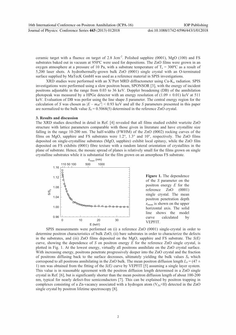
ceramic target with a fluence on target of 2.8 Jcm-2. Polished sapphire (0001), MgO (100) and FS substrates baked out in vacuum at 950ºC were used for depositions. The ZnO films were grown in an oxygen atmosphere at a pressure of 10 Pa, with a substrate temperature of Ts = 300ºC as a result of 5,200 laser shots. A hydrothermally-grown bulk ZnO (0001) single crystal with an O-terminated surface supplied by MaTecK GmbH was used as a reference material in SPIS investigations. XRD studies were performed with an X’Pert MRD diffractometer using Cu-K� radiation. SPIS investigations were performed using a slow positron beam, SPONSOR [3], with the energy of incident positrons adjustable in the range from 0.03 to 36 keV. Doppler broadening (DB) of the annihilation photopeak was measured by a HPGe detector with an energy resolution of (1.09 ± 0.01) keV at 511 keV. Evaluation of DB was perfor using the line shape S parameter. The central energy region for the calculation of S was chosen as |E – m0c2| < 0.93 keV and all the S parameters presented in this paper are normalized to the bulk value S0 = 0.5068(5) determined in the reference ZnO crystal. 3. Results and discussion The XRD studies described in detail in Ref. [4] revealed that all films studied exhibit wurtzite ZnO structure with lattice parameters comparable with those given in literature and have crystallite size falling in the range 10-200 nm. The half-widths (FWHM) of the ZnO (0002) rocking curves of the films on MgO, sapphire and FS substrates were 1.2°, 1.3° and 10°, respectively. The ZnO films deposited on single-crystalline substrates (MgO, sapphire) exhibit local epitaxy, while the ZnO film deposited on FS exhibits (0001) fibre texture with a random lateral orientation of crystallites in the plane of substrate. Hence, the mosaic spread of planes is relatively small for the films grown on single crystalline substrates while it is substantial for the film grown on an amorphous FS substrate.
E (keV)0 10 20 30
S/S 0
0.96
1.00
1.04
1.08
1.12
1.16
zmean (nm)110 50 100 500 1000
Figure 1. The dependence of the S parameter on the positron energy E for the reference ZnO (0001) single crystal. The mean positron penetration depth zmean is shown on the upper horizontal axis. The solid line shows the model curve calculated by VEPFIT.
SPIS measurements were performed on (i) a reference ZnO (0001) single-crystal in order to determine positron characteristics of bulk ZnO, (ii) bare substrates in order to characterize the defects in the substrates, and (iii) ZnO films deposited on the MgO, sapphire and FS substrate. The S(E) curve, showing the dependence of S on positron energy E for the reference ZnO single crystal, is plotted in Fig. 1. At the lowest energy, virtually all positrons annihilate on the ZnO crystal surface. With increasing energy, positrons penetrate progressively deeper into the ZnO crystal and the fraction of positrons diffusing back to the surface decreases, ultimately yielding the bulk values S0 which correspond to all positrons annihilating in the ZnO bulk. The mean positron diffusion length L0 = (47 ± 1) nm was obtained from the fitting of the S(E) curve by VEPFIT [5] assuming a single layer system. This value is in reasonable agreement with the positron diffusion length determined in a ZnO single crystal in Ref. [6], but is significantly shorter than the mean positron diffusion length of about 100-200 nm, typical for nearly defect-free semiconductors [7]. This can be explained by positron trapping in complexes consisting of a Zn-vacancy associated with a hydrogen atom (VZn+H) detected in the ZnO single crystal by positron lifetime spectroscopy [8].
16th International Conference on Positron Annihilation (ICPA-16) IOP PublishingJournal of Physics: Conference Series 443 (2013) 012018 doi:10.1088/1742-6596/443/1/012018
2
S/S
0
0.95
1.00
1.05
1.10
1.15
1.20
1.25
E (keV)0 10 20 30
ZnO film on MgOZnO film on FSZnO film on sapphireMgO substrateFS substratesapphire substrate
A zmean (nm)1 10 50 100 500 1000
B zmean (nm)1 10 50 100 500 1000
E (keV)0 10 20 30
S/S 0
0.95
1.00
1.05
1.10
1.15
1.20
1.25
FS substrateMgO substratesapphire substrate
Figure 2. Dependence of the S parameter on positron energy for (A) bare substrates and (B) ZnO films. The mean positron penetration depth zmean is shown on the upper horizontal axis. Dashed and solid lines show model curves calculated by VEPFIT for bare substrates and ZnO films, respectively.
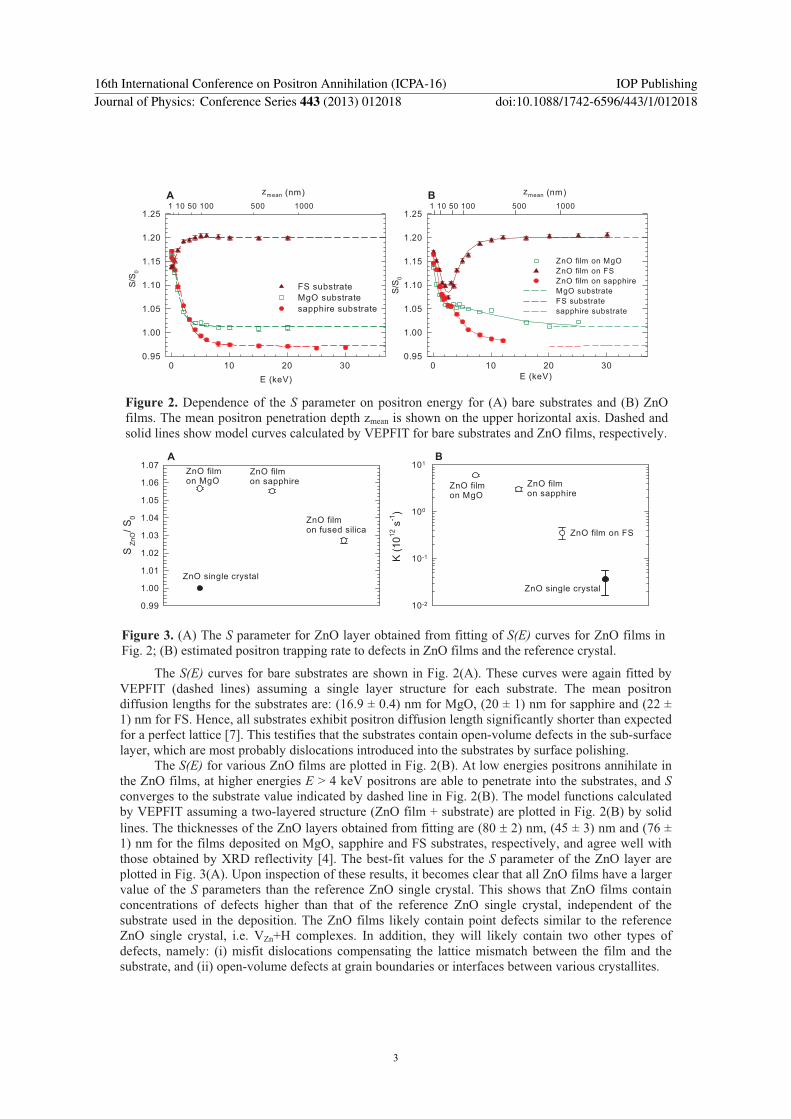
The S(E) curves for bare substrates are shown in Fig. 2(A). These curves were again fitted by VEPFIT (dashed lines) assuming a single layer structure for each substrate. The mean positron diffusion lengths for the substrates are: (16.9 ± 0.4) nm for MgO, (20 ± 1) nm for sapphire and (22 ± 1) nm for FS. Hence, all substrates exhibit positron diffusion length significantly shorter than expected for a perfect lattice [7]. This testifies that the substrates contain open-volume defects in the sub-surface layer, which are most probably dislocations introduced into the substrates by surface polishing. The S(E) for various ZnO films are plotted in Fig. 2(B). At low energies positrons annihilate in the ZnO films, at higher energies E > 4 keV positrons are able to penetrate into the substrates, and S converges to the substrate value indicated by dashed line in Fig. 2(B). The model functions calculated by VEPFIT assuming a two-layered structure (ZnO film + substrate) are plotted in Fig. 2(B) by solid lines. The thicknesses of the ZnO layers obtained from fitting are (80 � 2) nm, (45 ± 3) nm and (76 ± 1) nm for the films deposited on MgO, sapphire and FS substrates, respectively, and agree well with those obtained by XRD reflectivity [4]. The best-fit values for the S parameter of the ZnO layer are plotted in Fig. 3(A). Upon inspection of these results, it becomes clear that all ZnO films have a larger value of the S parameters than the reference ZnO single crystal. This shows that ZnO films contain concentrations of defects higher than that of the reference ZnO single crystal, independent of the substrate used in the deposition. The ZnO films likely contain point defects similar to the reference ZnO single crystal, i.e. VZn+H complexes. In addition, they will likely contain two other types of defects, namely: (i) misfit dislocations compensating the lattice mismatch between the film and the substrate, and (ii) open-volume defects at grain boundaries or interfaces between various crystallites.
S ZnO
/ S0
0.99
1.00
1.01
1.02
1.03
1.04
1.05
1.06
1.07
K (1
012 s
-1)
10-2
10-1
100
101
ZnO single crystal
ZnO filmon MgO
ZnO film on sapphire
ZnO filmon fused silica
ZnO single crystal
ZnO filmon MgO
ZnO film on sapphire
ZnO film on FS
A B
Figure 3. (A) The S parameter for ZnO layer obtained from fitting of S(E) curves for ZnO films in Fig. 2; (B) estimated positron trapping rate to defects in ZnO films and the reference crystal.
16th International Conference on Positron Annihilation (ICPA-16) IOP PublishingJournal of Physics: Conference Series 443 (2013) 012018 doi:10.1088/1742-6596/443/1/012018
3
The positron trapping rate K in defects is proportional to the net concentration of defects in ZnO films. This quantity can be estimated from the expression [7] K = 1/�B [(L+,B / L+)2-1], where �B = 154 ps is the bulk positron lifetime [8], L+,B is the positron diffusion length in defect-free ZnO, and L+ is the positron diffusion length measured in the ZnO film. Since defect-free ZnO crystals are not available L+,B � 150 nm was estimated from expression L+,B = (D+ �B)1/2 using the positron diffusion coefficient D+ � 1.6 cm2s-1 estimated from the formula D+ = 1/3 <l> (<v2>)1/2, where <l> � 5 nm is the mean free path between positron scattering events by longitudinal acoustic phonons determined for defect-free semiconductors GaAs and Ge in Ref. [9] and <v2> is the mean square thermal positron velocity [7]. From inspection of estimated trapping rates in Fig. 3(B), it becomes clear that all the ZnO films studied exhibit higher defect concentration than the reference ZnO single crystal. Moreover, the defect densities in the films deposited on the single crystalline substrates (MgO and sapphire) are higher than the concentration of defects in the film deposited on the FS substrate. In the ZnO film deposited on the FS substrate, the mismatch between atomic positions in the substrate and in the film is, to some extent, compensated for by many differing orientations (tilting) of the ZnO crystallites. As a consequence, the density of misfit dislocations in ZnO crystallites is relatively low and positrons are trapped predominantly in open volume misfit defects at the interfaces between the crystallites. On the other hand, ZnO films deposited on MgO and sapphire single crystalline substrates exhibit local epitaxy. In these cases, the lattice mismatch between the film and the substrate accumulates mainly by misfit dislocations. Finally, it should be mentioned that the width of the rocking curve, which is often used for characterization of quality of epitaxial thin films, is a measure of the perfection of the structural relationship but is not directly correlated with the density of defects in the film. From comparison of XRD and SPIS results in this work, we can conclude that ZnO films deposited on single crystalline substrates (MgO and sapphire) exhibit narrow rocking curves, but concentration of defects in these films is substantially higher than in the film deposited on the amorphous FS, substrate which is characterized by significantly wider rocking curve. 4. Conclusions Very thin ZnO films deposited by PLD on various substrates were characterized. All films exhibit higher concentrations of open volume defects than a bulk ZnO single crystal. The ZnO films deposited on the single crystalline substrates (MgO, sapphire) exhibit a higher concentration of defects than film deposited on an amorphous FS substrate. This is most probably due to a higher density of misfit dislocations, which compensate for the lattice mismatch between the film and the substrate. 5. References [1] Bagnall B M, Chen Y F, Zhu Z, Yao T, Koyama S, Shen M Y and Goto T 1997 Appl. Phys.
Lett. 70 2230 [2] Hu W S, Liu Z G, Sun J, Zhu S N, Xu Q Q, Feng D and Ji Z M 1997 J. Phys. Chem. Sol. 58 853 [3] Anwand W, Kissener H R and Brauer G 1995 Acta Physica Polonica A 88 7 [4] Novotný M et al. 2012 J. Phys. D, 45 225101 [5] v Veen A, Schut H, Clement M, de Nijs J, Kruseman A and Ijpma M 1995 Appl Surf Sci 85 216 [6] Koida T, Uedono A, Tsukazaki A, Sota T, Kawasaki M and Chichibu S F 2004 phys. stat. sol.
(a) 201 2841 [7] Krause-Rehberg R and Leipner H S 1999 Positron Annihilation in Semiconductors – Defect
Studies, Springer, Berlin [8] Brauer G et al. 2009 Phys. Rev. B 79 115212 [9] Soininen E, Mäkinen J, Beyer D and Hautojärvi P 1992 Phys. Rev. B 46 13104 Acknowledgments This work was supported by the Czech Science agency (project P108/11/0958), the Czech Ministry of Education, Youths and Sports (project MEB101102) and DAAD (project 50755628).
16th International Conference on Positron Annihilation (ICPA-16) IOP PublishingJournal of Physics: Conference Series 443 (2013) 012018 doi:10.1088/1742-6596/443/1/012018
4