OP77 (Rev. G)
17
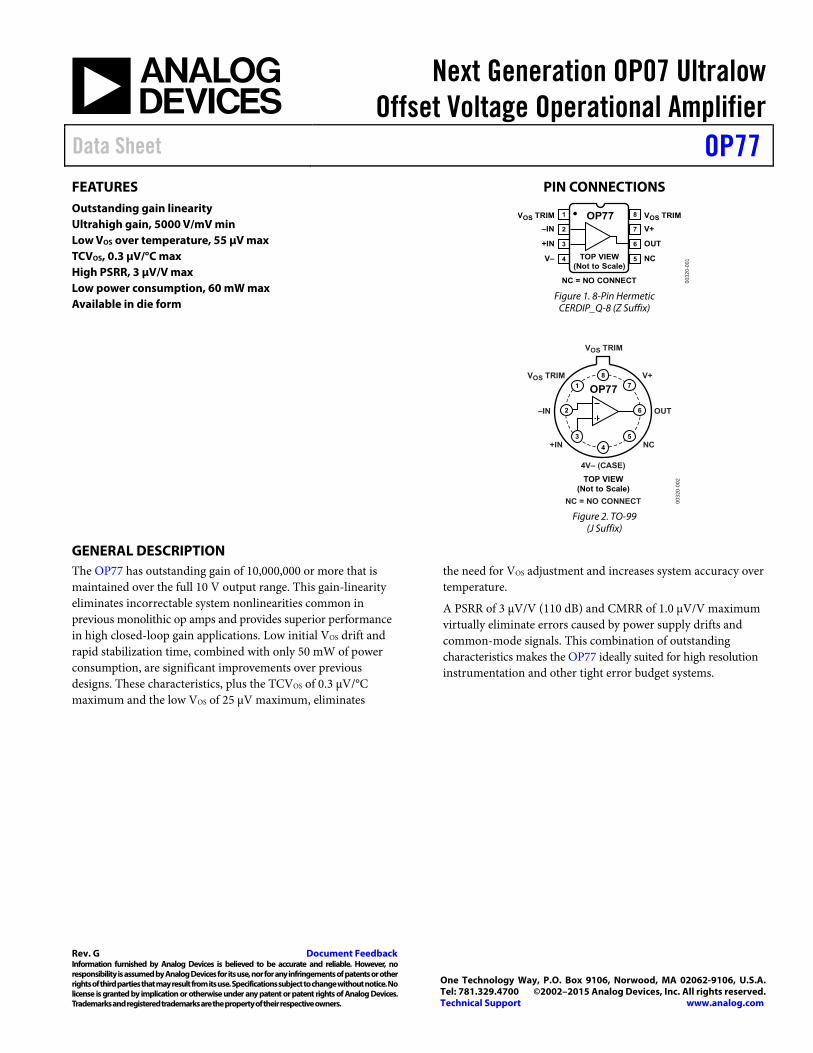
Next Generation OP07 Ultralow Offset Voltage Operational Amplifier Data Sheet OP77 Rev. G Document Feedback Information furnished by Analog Devices is believed to be accurate and reliable. However, no responsibility is assumed by Analog Devices for its use, nor for any infringements of patents or other rights of third parties that may result from its use. Specifications subject to change without notice. No license is granted by implication or otherwise under any patent or patent rights of Analog Devices. Trademarks and registered trademarks are the property of their respective owners. One Technology Way, P.O. Box 9106, Norwood, MA 02062-9106, U.S.A. Tel: 781.329.4700 ©2002–2015 Analog Devices, Inc. All rights reserved. Technical Support www.analog.com FEATURES Outstanding gain linearity Ultrahigh gain, 5000 V/mV min Low VOS over temperature, 55 μV max TCVOS, 0.3 μV/°C max High PSRR, 3 μV/V max Low power consumption, 60 mW max Available in die form PIN CONNECTIONS V OS TRIM 1 –IN 2 +IN 3 V– 4 V OS TRIM 8 V+ 7 OUT 6 NC 5 NC = NO CONNECT OP77 TOP VIEW (Not to Scale) 00320-001 Figure 1. 8-Pin Hermetic CERDIP_Q-8 (Z Suffix) V OS TRIM V OS TRIM V+ 4V– (CASE) +IN NC NC = NO CONNECT –IN OUT 00320-002 OP77 TOP VIEW (Not to Scale) 7 3 1 5 6 2 8 4 Figure 2. TO-99 (J Suffix) GENERAL DESCRIPTION The OP77 has outstanding gain of 10,000,000 or more that is maintained over the full 10 V output range. This gain-linearity eliminates incorrectable system nonlinearities common in previous monolithic op amps and provides superior performance in high closed-loop gain applications. Low initial VOS drift and rapid stabilization time, combined with only 50 mW of power consumption, are significant improvements over previous designs. These characteristics, plus the TCVOS of 0.3 μV/°C maximum and the low VOS of 25 μV maximum, eliminates the need for VOS adjustment and increases system accuracy over temperature. A PSRR of 3 μV/V (110 dB) and CMRR of 1.0 μV/V maximum virtually eliminate errors caused by power supply drifts and common-mode signals. This combination of outstanding characteristics makes the OP77 ideally suited for high resolution instrumentation and other tight error budget systems.
Transcript of OP77 (Rev. G)
Next Generation OP07 Ultralow Offset Voltage Operational Amplifier
Data Sheet OP77
Rev. G Document Feedback Information furnished by Analog Devices is believed to be accurate and reliable. However, no responsibility is assumed by Analog Devices for its use, nor for any infringements of patents or other rights of third parties that may result from its use. Specifications subject to change without notice. No license is granted by implication or otherwise under any patent or patent rights of Analog Devices. Trademarks and registered trademarks are the property of their respective owners.
One Technology Way, P.O. Box 9106, Norwood, MA 02062-9106, U.S.A.Tel: 781.329.4700 ©2002–2015 Analog Devices, Inc. All rights reserved. Technical Support www.analog.com
FEATURES Outstanding gain linearity Ultrahigh gain, 5000 V/mV min Low VOS over temperature, 55 μV max TCVOS, 0.3 μV/°C max High PSRR, 3 μV/V max Low power consumption, 60 mW max Available in die form
PIN CONNECTIONS
VOS TRIM 1
–IN 2
+IN 3
V– 4
VOS TRIM8
V+7
OUT6
NC5
NC = NO CONNECT
OP77
TOP VIEW(Not to Scale)
0032
0-00
1
Figure 1. 8-Pin Hermetic
CERDIP_Q-8 (Z Suffix)
VOS TRIM
VOS TRIM V+
4V– (CASE)
+IN NC
NC = NO CONNECT
–IN OUT
0032
0-00
2
OP77
TOP VIEW(Not to Scale)
7
3
1
5
62
8
4
Figure 2. TO-99
(J Suffix)
GENERAL DESCRIPTION The OP77 has outstanding gain of 10,000,000 or more that is maintained over the full 10 V output range. This gain-linearity eliminates incorrectable system nonlinearities common in previous monolithic op amps and provides superior performance in high closed-loop gain applications. Low initial VOS drift and rapid stabilization time, combined with only 50 mW of power consumption, are significant improvements over previous designs. These characteristics, plus the TCVOS of 0.3 μV/°C maximum and the low VOS of 25 μV maximum, eliminates
the need for VOS adjustment and increases system accuracy over temperature.
A PSRR of 3 μV/V (110 dB) and CMRR of 1.0 μV/V maximum virtually eliminate errors caused by power supply drifts and common-mode signals. This combination of outstanding characteristics makes the OP77 ideally suited for high resolution instrumentation and other tight error budget systems.

OP77* PRODUCT PAGE QUICK LINKSLast Content Update: 02/23/2017
COMPARABLE PARTSView a parametric search of comparable parts.
DOCUMENTATIONApplication Notes
• AN-106: A Collection of Amp Applications
• AN-649: Using the Analog Devices Active Filter Design Tool
Data Sheet
• OP77: Next Generation OP07 Ultralow Offset Voltage Operational Data Sheet
DESIGN RESOURCES• OP77 Material Declaration
• PCN-PDN Information
• Quality And Reliability
• Symbols and Footprints
DISCUSSIONSView all OP77 EngineerZone Discussions.
SAMPLE AND BUYVisit the product page to see pricing options.
TECHNICAL SUPPORTSubmit a technical question or find your regional support number.
DOCUMENT FEEDBACKSubmit feedback for this data sheet.
This page is dynamically generated by Analog Devices, Inc., and inserted into this data sheet. A dynamic change to the content on this page will not trigger a change to either the revision number or the content of the product data sheet. This dynamic page may be frequently modified.

OP77 Data Sheet
Rev. G | Page 2 of 16
TABLE OF CONTENTS Features .............................................................................................. 1
Pin Connections ............................................................................... 1
General Description ......................................................................... 1
Revision History ............................................................................... 2
Specifications ..................................................................................... 3
Electrical Specifications ............................................................... 3
Wafer Test Limits .......................................................................... 4
Typical Electrical Characteristics ............................................... 5
Absolute Maximum Ratings ............................................................ 6
Thermal Resistance .......................................................................6
ESD Caution...................................................................................6
Typical Performance Characteristics ..............................................7
Test Circuits ..................................................................................... 10
Applications ..................................................................................... 11
Precision Current Sinks ............................................................. 12
Outline Dimensions ....................................................................... 15
Ordering Guide .......................................................................... 16
REVISION HISTORY 10/15—Rev. F to Rev. G Changes to Features Section and General Description Section ..... 1 Changes to Note 1, Ordering Guide.................................................. 16 3/15—Rev. E to Rev. F Updated Outline Dimensions ....................................................... 15 Changes to Ordering Guide .......................................................... 16 4/10—Rev. D to Rev. E Removed Figure 33 and Two Subsequent Paragraphs ............... 12 6/09—Rev. C to Rev. D Changes to Figure 1 and Figure 2 ................................................... 1 Changes to Table 1 ............................................................................ 3 Removed Endnote 1 and Endnote 2 in Table 3 ............................ 4 Changes to Figure 16 ........................................................................ 9 Changes to Figure 31 and Figure 32 ............................................. 12 Changes to Figure 38 ...................................................................... 14 Moved Figure 39 ............................................................................. 14 10/02—Rev. B to Rev. C Edits to Specifications ...................................................................... 2 Figure 2 Caption Changed ............................................................ 10 Figure 3 Caption Changed ............................................................ 10 Edits to Figure 10 ............................................................................ 11 Updated Outline Dimensions ....................................................... 15 2/02—Rev. A to Rev. B Remove 8-Lead SO PIN Connection Diagrams ........................... 1 Changes to Absolute Maximum Rating ......................................... 2 Remove OP77B column from Specifications ................................ 2 Remove OP77B column from Electrical Characteristics ........ 3, 5 Remove OP77G column from Wafer Test Limits ......................... 6 Remove OP77G column from Typical Electrical Characteristics .... 6

Data Sheet OP77
Rev. G | Page 3 of 16
SPECIFICATIONS ELECTRICAL SPECIFICATIONS @ VS = ±15 V, TA = 25°C, unless otherwise noted.
Table 1. OP77E OP77F Parameter Symbol Conditions Min Typ Max Min Typ Max Unit INPUT OFFSET VOLTAGE VOS 10 25 20 60 μV LONG-TERM STABILITY1 VOS/time 0.3 0.4 μV/Mo INPUT OFFSET CURRENT IOS 0.3 1.5 0.3 2.8 nA INPUT BIAS CURRENT IB −0.2 +1.2 +2.0 −0.2 +1.2 +2.8 nA INPUT NOISE VOLTAGE2 enp-p 0.1 Hz to 10 Hz 0.35 0.6 0.38 0.65 μVp-p INPUT NOISE VOLTAGE DENSITY en fO = 10 Hz 10.3 18.0 10.5 20.0 nV/√Hz fO = 100 Hz2 10.0 13.0 10.2 13.5 fO = 1000 Hz 9.6 11.0 9.8 11.5 INPUT NOISE CURRENT2 inp-p 0.1 Hz to 10 Hz 14 30 15 35 pAp-p INPUT NOISE CURRENT DENSITY in fO = 10 Hz 0.32 0.80 0.35 0.90 pA√Hz fO = 100 Hz2 0.14 0.23 0.15 0.27 fO = 1000 Hz 0.12 0.17 0.13 0.18 INPUT RESISTANCE
Differential Mode3 RIN 26 45 18.5 45 MΩ Common Mode RINCM 200 200 GΩ
INPUT VOLTAGE RANGE IVR ±13 ±14 ±13 ±14 V COMMON-MODE REJECTION RATIO CMRR VCM = ±13 V 0.1 1.0 0.1 1.6 μV/V POWER SUPPLY REJECTION RATIO PSRR VS = ±3 V to ±18 V 0.7 3.0 0.7 3.0 μV/V LARGE-SIGNAL VOLTAGE GAIN AVO RL ≥ 2 kΩ 5000 12,000 2000 6000 V/mV VO = ±10 V OUTPUT VOLTAGE SWING VO RL ≥ 10 kΩ ±13.5 ±14.0 ±13.5 ±14.0 V RL ≥ 2 kΩ ±12.5 ±13.0 ±12.5 ±13.0 RL ≥ 1 kΩ ±12.0 ±12.5 ±12.0 ±12.5 SLEW RATE2 SR RL ≥ 2 kΩ 0.1 0.3 0.1 0.3 V/μs CLOSED-LOOP BANDWIDTH2 BW AVCL + 1 0.4 0.6 0.4 0.6 MHz OPEN-LOOP OUTPUT RESISTANCE RO 60 60 Ω POWER CONSUMPTION Pd VS = ±15 V, no load 50 60 50 60 mW VS = ±3 V, no load 3.5 4.5 3.5 4.5 OFFSET ADJUSTMENT RANGE Rp = 20 kn ±3 ±3 mV 1 Long-term input offset voltage stability refers to the averaged trend line of VOS vs. time over extended periods after the first 30 days of operation. Excluding the initial
hour of operation, changes in VOS during the first 30 operating days are typically 2.5 μV. 2 Sample tested. 3 Guaranteed by design.

OP77 Data Sheet
Rev. G | Page 4 of 16
@ VS = ±15 V, −25°C ≤ TA ≤ +85°C for OP77FJ and OP77E/OP77F, unless otherwise noted.
Table 2. OP77E OP77F Parameter Symbol Conditions Min Typ Max Min Typ Max Unit INPUT OFFSET VOLTAGE VOS 10 45 20 100 µV AVERAGE INPUT OFFSET VOLTAGE DRIFT1 TCVOS 0.1 0.3 0.2 0.6 µV/°C INPUT OFFSET CURRENT IOS 0.5 2.2 0.5 4.5 nA AVERAGE INPUT OFFSET CURRENT DRIFT2 TCIOS 1.5 4.0 1.5 85 pA/°C INPUT BIAS CURRENT IB −0.2 +2.4 +4.0 −0.2 +2.4 +6.0 nA AVERAGE INPUT BIAS CURRENT DRIFT2 TCIB 8 40 15 60 pA/°C INPUT VOLTAGE RANGE IVR ±13.0 ±13.5 ±13.0 ±13.5 V COMMON-MODE REJECTION RATIO CMRR VCM = ±13 V 0.1 1.0 0.1 3.0 pV/V POWER SUPPLY REJECTION RATIO PSRR VS = ±3 V to ±18 V 1.0 3.0 1.0 5.0 µV/V LARGE-SIGNAL VOLTAGE GAIN AVO RL ≥ 2 kΩ 2000 6000 1000 4000 V/mV VO = ±10 V OUTPUT VOLTAGE SWING VO RL ≥ 2 kΩ ±12 ±13.0 ±12 ±13.0 V POWER CONSUMPTION Pd VS = ±15 V, no load 60 75 60 75 mW 1 OP77E: TCVOS is 100% tested on J and Z packages. 2 Guaranteed by end-point limits.
WAFER TEST LIMITS @ VS = ±15 V, TA = 25°C, for OP77NBC devices, unless otherwise noted.
Table 3. Parameter Symbol Conditions OP77NBC Limit Unit INPUT OFFSET VOLTAGE VOS 40 µV max INPUT OFFSET CURRENT IOS 2.0 nA max INPUT BIAS CURRENT IB ±2 nA max INPUT RESISTANCE
Differential Mode RIN 26 MΩ min INPUT VOLTAGE RANGE IVR ±13 V min COMMON-MODE REJECTION RATIO CMRR VCM = ±13 V 1 µV/V max POWER SUPPLY REJECTION RATIO PSRR VS = ±3 V to ±18 V 3 µV/V max OUTPUT VOLTAGE SWING VO RL = 10 kΩ ±13.5 V min RL = 2 kΩ ±12.5 RL = 1 kΩ ±12.0 LARGE-SIGNAL VOLTAGE GAIN AVO RL = 2 kΩ 2000 V/mV min VO = ±10 V DIFFERENTIAL INPUT VOLTAGE ±30 V max POWER CONSUMPTION Pd VO = 0 V 60 mW max

Data Sheet OP77
Rev. G | Page 5 of 16
TYPICAL ELECTRICAL CHARACTERISTICS @ VS = ±15 V, TA = 25°C, unless otherwise noted.
Table 4. Parameter Symbol Conditions OP77NBC Limit Unit AVERAGE INPUT OFFSET VOLTAGE DRIFT TCVOS RS = 50 Ω 0.1 µV/°C NULLED INPUT OFFSET VOLTAGE DRIFT TCVOSn RS = 50 Ω, RP = 20 kΩ 0.1 µV/°C AVERAGE INPUT OFFSET CURRENT DRIFT TCIOS 0.5 pA/°C SLEW RATE SR RL ≥ 2 kΩ 0.3 V/µs BANDWIDTH BW AVCL + 1 0.6 MHz
OP77 Data Sheet
Rev. G | Page 6 of 16
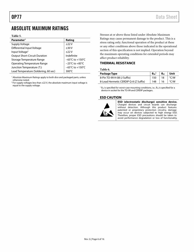
ABSOLUTE MAXIMUM RATINGS Table 5. Parameter1 Rating Supply Voltage ±22 V Differential Input Voltage ±30 V Input Voltage2 ±22 V Output Short-Circuit Duration Indefinite Storage Temperature Range −65°C to +150°C Operating Temperature Range −25°C to +85°C Junction Temperature (TJ) −65°C to +150°C Lead Temperature (Soldering, 60 sec) 300°C
1 Absolute Maximum Ratings apply to both dice and packaged parts, unless otherwise noted.
2 For supply voltages less than ±22 V, the absolute maximum input voltage is equal to the supply voltage.
Stresses at or above those listed under Absolute Maximum Ratings may cause permanent damage to the product. This is a stress rating only; functional operation of the product at these or any other conditions above those indicated in the operational section of this specification is not implied. Operation beyond the maximum operating conditions for extended periods may affect product reliability.
THERMAL RESISTANCE
Table 6. Package Type θJA
1 θJC Unit 8-Pin TO-99 H-08 (J Suffix) 150 18 °C/W 8-Lead Hermetic CERDIP Q-8 (Z Suffix) 148 16 °C/W
1 θJA is specified for worst-case mounting conditions, i.e., θJA is specified for a device in socket for the TO-99 and CERDIP packages.
ESD CAUTION

Data Sheet OP77
Rev. G | Page 7 of 16
TYPICAL PERFORMANCE CHARACTERISTICS 2
1
0
–1
–2–10 –5 0 5 10
OUTPUT VOLTAGE (V)
INP
UT
VO
LT
AG
E (
µV
)(N
UL
LE
D T
O 0
µV
@ V
OU
T =
0V
)
0032
0-00
4
VS = ±15VTA = 25°CRL = 10kΩ
Figure 3. Gain Linearity (Input Voltage vs. Output Voltage)
25
20
15
10
5
0–55 –35 –15 5 25 45 65 85 105 125
TEMPERATURE (°C)
OP
EN
-LO
OP
GA
IN (
V/µ
V)
0032
0-00
5
VS = ±15V
Figure 4. Open-Loop Gain vs. Temperature
16
12
8
4
00 ±5 ±10 ±15 ±20
POWER SUPPLY VOLTAGE (V)
OP
EN
-LO
OP
GA
IN (
V/µ
V)
0032
0-00
6
TA = 25°CRL = 2kΩ
Figure 5. Open-Loop Gain vs. Power Supply Voltage
30
20
10
0
–10
–20
–30–55 –35 –15 5 25 45 65 85 105 125
TEMPERATURE (°C)
CH
AN
GE
IN
OF
FS
ET
VO
LT
AG
E (
µV
)
0032
0-00
7
J, Z PACKAGES+0.3µV/°C
MEANS.D.
–0.3µV/°C
Figure 6. Untrimmed Offset Voltage vs. Temperature
4
3
2
1
0
–1
–2
–3
–40 0.5 1.0 1.5 2.0 2.5 3.0 3.5
TIME AFTER POWER SUPPLY TURN-ON (Minutes)
CH
AN
GE
IN
IN
PU
T O
FF
SE
T V
OL
TA
GE
(µ
V)
0032
0-00
8
VS = ±15VTA = 25°C
Figure 7. Warm-Up Drift
30
25
20
15
10
5
0–10 0 10 20 30 40 50 60 70
TIME (Seconds)
AB
SO
LU
TE
CH
AN
GE
IN
IN
PU
TO
FF
SE
T V
OL
TA
GE
(µ
V)
0032
0-00
9
VS = ±15V
DEVICE IMMERSED IN70°C OIL BATH (20 UNITS)
MAXIMUM
MIMIMUM
AVERAGE
Figure 8. Offset Voltage Change Due to Thermal Shock

OP77 Data Sheet
Rev. G | Page 8 of 16
100
80
60
40
20
0
–2010 100 1k 10k 100k 1M 10M
FREQUENCY (Hz)
CLO
SED
-LO
OP
GA
IN (d
B)
0032
0-01
0
VS = ±15VTA = 25°C
Figure 9. Closed-Loop Response for Various Gain Configurations
160
140
120
100
80
60
40
20
0
0
45
90
135
1800.01 0.1 1 10 100 1k 10k 100k 1M
FREQUENCY (Hz)
OPE
N-L
OO
P G
AIN
(dB
)
PHA
SE (D
egre
es)
0032
0-01
1
VS = ±15VTA = 25°C
Figure 10. Open-Loop Gain/Phase Response
150
140
130
120
110
100
90
801 10 100 1k 10k 100k
FREQUENCY (Hz)
CM
MR
(dB
)
0032
0-01
2
TA = 25°C
Figure 11. CMRR vs. Frequency
130
120
110
100
90
80
70
600.1 1 10 100 1k 10k
FREQUENCY (Hz)
PSR
R (d
B)
0032
0-01
3
TA = 25°C
Figure 12. PSRR vs. Frequency
4
3
2
1
0–75 –50 –25 0 25 50 75 100 125
TEMPERATURE (°C)
INPU
T B
IAS
CU
RR
ENT
(nA
)
0032
0-01
4
VS = ±15V
Figure 13. Input Bias Current vs. Temperature
2.0
1.5
1.0
0.5
0–75 –50 –25 0 25 50 75 100 125
TEMPERATURE (°C)
INPU
T O
FFSE
T C
UR
REN
T (n
A)
0032
0-01
5
VS = ±15V
Figure 14. Input Offset Current vs. Temperature

Data Sheet OP77
Rev. G | Page 9 of 16
10
1
0.1100 1k 10k 100k
FREQUENCY (Hz)
RM
S N
OIS
E (m
V)
0032
0-01
6
VS = ±15VTA = 25°C
Figure 15. Input Wideband Noise vs. Bandwidth (0.1 Hz to Frequency
Indicated)
1k
100
10
11 10 100 1k
FREQUENCY (Hz)
INPU
T NO
ISE
VOLT
AGE
(nV/
Hz)
0032
0-01
7
VS = ±15VTA = 25°C
RESISTORSINCLUDED
EXCLUDED
RS = 0
RS1 = RS2 = 200kΩTHERMAL NOISE OF SOURCE
Figure 16. Total Input Noise Voltage vs. Frequency
32
28
24
20
16
12
8
4
01k 10k 100k 1M
FREQUENCY (Hz)
PEA
K-T
O-P
EAK
AM
PLIT
UD
E (V
)
0032
0-01
8
VS = ±15VTA = 25°C
Figure 17. Maximum Output Swing vs. Frequency
100
10
10 10 20 30 40
TOTAL SUPPLY VOLTAGE V+ TO V– (V)
POW
ER C
ON
SUM
PTIO
N (m
W)
0032
0-01
9
TA = 25°C
Figure 18. Power Consumption vs. Power Supply
20
15
10
5
0100 1k 10k
LOAD RESISTANCE TO GROUND (Ω)
MA
XIM
UM
OU
TPU
T (V
)
0032
0-02
0
VS = ±15VTA = 25°CVIN = ±10mV
POSITIVE SWING
NEGATIVE SWING
Figure 19. Maximum Output Voltage vs. Load Resistance
40
35
30
25
20
150 1 2 3 4
TIME FROM OUTPUT BEING SHORTENED (Minutes)
OU
TPU
T SH
OR
T-C
IRC
UIT
CU
RR
ENT
(mA
)
0032
0-02
1
VS = ±15VTA = 25°C
Figure 20. Output Short-Circuit Current vs. Time

OP77 Data Sheet
Rev. G | Page 10 of 16
TEST CIRCUITS
OP77
200kΩ
VO
50Ω
VOS =VO
4000 0032
0-02
2
Figure 21. Typical Offset Voltage Test Circuit
INPUT REFERRED NOISE =VO
25,000 0032
0-02
3OP77
2.5MΩ
V+
V–
OUTPUT
100Ω
100Ω3.3kΩ
4.7µF(≈10Hz FILTER)
76
4
2
3
Figure 22. Typical Low-Frequency Noise Test Circuit
0032
0-02
4
OP77
V+
OUTPUT
V–
20kΩ
INPUT+
–1
87 6
4
2
3
Figure 23. Optional Offset Nulling Circuit
0032
0-02
5
OP77
100kΩ
+18V
–18V
76
4
2
3
+10µF
+10µF
0.1µF
0.1µF
*
*
10Ω
10Ω10kΩ10kΩ
NOTES*1 PER BOARD
Figure 24. Burn-In Circuit
1MΩ
RL
VX10Ω
10kΩ 100kΩ
VIN = ±10V
TYPICAL PRECISIONOP AMP
VY
VX
–10V 0V +10V
NOTES1. GAIN NOT CONSISTANT. CAUSES NONLINEAR ERRORS.2. AVO SPEC IS ONLY PART OF THE SOLUTION.3. CHECK SPECIFICATION TABLE 1 AND TABLE 2 FOR PERFORMANCE. 00
320-
026
AVO 650V/mVRL = 2kΩ
Figure 25. Open-Loop Gain Linearity
Actual open-loop voltage gain can vary greatly at various output voltages. All automated testers use endpoint testing and therefore only show the average gain. This causes errors in high closed-loop gain circuits. Because this is difficult for manufacturers to test, users should make their own evaluations. This simple test circuit makes it easy. An ideal op amp would show a horizontal scope trace.
VY
VX–10V 0V +10V
0032
0-02
7
Figure 26. Output Gain Linearity Trace
This is the output gain linearity trace for the new OP77. The output trace is virtually horizontal at all points, assuring extremely high gain accuracy. The average open-loop gain is truly impressive—approximately 10,000,000.

Data Sheet OP77
Rev. G | Page 11 of 16
APPLICATIONS
0032
0-02
8
OP77E
R21MΩ
R41MΩ
+15V
–15V
R11kΩ
R31kΩ
76
4
2
3
0.1µF
0.1µF
Figure 27. Precision High-Gain Differential Amplifier
The high gain, gain linearity, CMRR, and low TCVOS of the OP77 make it possible to obtain performance not previously available in single-stage, very high-gain amplifier applications.
For best CMR, 2R1R must equal
4R3R . In this example, with a
10 mV differential signal, the maximum errors are as listed in Table 7.
Table 7. Maximum Errors Type Amount Common-Mode Voltage 0.01%/V Gain Linearity, Worst Case 0.02% TCVOS 0.003%/°C TCIOS 0.008%/°C
0032
0-02
9
+15V
–15V
RS
RF
100Ω7
6
4
2
3
0.1µF
0.1µF
10µF
OUTPUTINPUT
CLOAD
OP77
Figure 28. Isolating Large Capacitive Loads
This circuit reduces maximum slew rate but allows driving capacitive loads of any size without instability. Because the boon resistor is inside the feedback loop, its effect on output impedance is reduced to insignificance by the high open-loop gain of the OP77.
0032
0-03
0
R1100kΩ
R31kΩ
R4990Ω
R510Ω
62
3
VINIOUT < 15mA
R2100kΩ
OP77
Figure 29. Basic Current Source
0032
0-03
1
R1
R3
+15V
–15VR4
R5
62N2222
2N2907
2
3
VIN
R2 OP77
IOUT = VIN ( )GIVEN R3 = R4 + R5, R1 = R2
R3R1 – R5
IOUT < 100mA
Figure 30. 100 mA Current Source
These current sources can supply both positive and negative current into a grounded load.
Note that
1R3R
2R4R5R2R4R5R
ZO +
+
=1
And that for ZO to be infinite 2R
4R5R + must =
1R3R

OP77 Data Sheet
Rev. G | Page 12 of 16
PRECISION CURRENT SINKS
0032
0-03
2
V+
200Ω
R11Ω1W
RL
IRF520
IOVIN
OP77
IO =
VIN > 0VFULL SCALE OF 1V.IO = 1A/V
VINR1
Figure 31. Positive Current Sink
0032
0-03
3
200Ω
RL
R1
IRF520
IO
VIN
V–
OP77IO =
VIN > 0V
VINR1
Figure 32. Positive Current Source
The simple high-current sinks, shown Figure 31 and Figure 32, require the load to float between the power supply and the sink.
In these circuits, the high gain, high CMRR, and low TCVOS of the OP77 ensure high accuracy.
The high gain and low TCVOS ensure accurate operation with inputs from microvolts to volts. In Figure 33, the signal always appears as a common-mode signal to the op amps. The OP77EZ CMRR of 1 µV/V ensures errors of less than 2 ppm.
0032
0-03
5
+15V
–15V
1kΩ 1kΩ
R32kΩ
C130pF
D11N4148
76
4
2
3
0.1µF
0.1µF
2N4393VIN
+15V
VOUT0 < VOUT < 10V
D2
–15V
76
4
2
3
0.1µF
0.1µF
OP77EOP77E
Figure 33. Precision Absolute Value Amplifier
0032
0-03
6
100ΩVOUT
15V
0.1µF
OP77
100Ω
100Ω
10µF
6
4
REF-01VO
2
6
4
REF-01VO
2
6
4
REF-01VO
2+
Figure 34. Low Noise Precision Reference

Data Sheet OP77
Rev. G | Page 13 of 16
Figure 34 relies upon low TCVOS of the OP77 and noise combined with very high CMRR to provide precision buffering of the averaged REF-01 voltage outputs.
In Figure 35, CH must be of polystyrene, Teflon*, or polyethylene to minimize dielectric absorption and leakage. The droop rate is determined by the size of CH and the bias current of the AD820. *Teflon is a registered trademark of the Dupont Company
0032
0-03
7
+15V
–15V
1kΩ
1kΩ 1kΩ
1N4148
76
4
2
3
0.1µF
0.1µF
2N930
CH
VIN
RESET
+15V
VOUT
–15V
76
4
2
3
0.1µF
0.1µF
AD820OP77
Figure 35. Precision Positive Peak Detector

OP77 Data Sheet
Rev. G | Page 14 of 16
0032
0-03
8
+15V
–15V
RS1kΩ
R12kΩ
CC
RF100kΩ
D11N4148
76
4
2
3
0.1µF
0.1µF
VOUT
VTH
VIN
OP77
Figure 36. Precision Threshold Detector/Amplifier
When VIN < VTH, amplifier output swings negative, reversing the biasing diode D1. VO = VTH if RL= ∞ when VIN > VTH, the loop closes,
( )
+−+=
S
FTHINTHO R
RVVVV 1
CC is selected to smooth the response of the loop.
0032
0-03
9
+15V
–15V
Ra
Rb1
2VIN
GND
VO
TRIM
TEMP
6
5
3
4 Rbp
1.5kΩ
50kΩ
Rc
0.1µF
0.1µF
VOUTOP77REF-02
Figure 37. Precision Temperature Sensor
Table 8. Resistor Values TCVOUT Slope (S) 10 mV/°C 100 mV/°C 10 mV/°F Temperature Range −55°C to
+125°C −55°C to +125°C
−67°F to +257°C
Output Voltage Range
−0.55 V to +1.25 V
−5.5 V to +12.5V
−0.67 V to +2.57V
Zero-Scale 0 V @ 0°C 0 V @ 0°C 0 V @ 0°F Ra (±1% Resistor) 9.09 kΩ 15 kΩ 7.5 kΩ Rb1 (±1% Resistor) 1.5 kΩ 1.82 kΩ 1.21 kΩ Rbp (Potentiometer) 200 Ω 500 Ω 200 Ω Rc (±1% Resistor) 5.11 kΩ 84.5 kΩ 8.25 kΩ
0032
0-00
3
7
1 8
3
2
4
OUTPUT6R9
R5
C3
C1
C2
R7
R8R6
Q19
Q18
Q20Q16
Q17
Q11 Q12
Q10Q9
Q13
Q27Q4Q3
Q8Q5
R3
R2A1
R1A
R2B1
R1B
R4
Q1Q23
Q7
Q24Q21Q22
Q6
Q2
Q26
Q25
Q14
Q15
R10
V+
V–
NONINVERTINGINPUT
INVERTINGINPUT
1R2A AND R2B ARE ELECTRONICALLY ADJUSTED ON CHIP AT FACTORY.
(OPTIONALNULL)
Figure 38. Simplified Schematic

Data Sheet OP77
Rev. G | Page 15 of 16
OUTLINE DIMENSIONS
CONTROLLING DIMENSIONS ARE IN INCHES; MILLIMETER DIMENSIONS(IN PARENTHESES) ARE ROUNDED-OFF INCH EQUIVALENTS FORREFERENCE ONLY AND ARE NOT APPROPRIATE FOR USE IN DESIGN.
0.310 (7.87)0.220 (5.59)
0.005 (0.13)MIN
0.055 (1.40)MAX
0.100 (2.54) BSC
15° 0°
0.320 (8.13)0.290 (7.37)
0.015 (0.38)0.008 (0.20)SEATING
PLANE
0.200 (5.08)MAX
0.405 (10.29) MAX
0.150 (3.81)MIN
0.200 (5.08)0.125 (3.18)0.023 (0.58)0.014 (0.36) 0.070 (1.78)
0.030 (0.76)
0.060 (1.52)0.015 (0.38)
1 4
58
Figure 39. 8-Lead Ceramic Dual In-Line Package [CERDIP]
(Q-8) Dimensions shown in inches and (millimeters)
CONTROLLING DIMENSIONS ARE IN INCHES; MILLIMETER DIMENSIONS(IN PARENTHESES) ARE ROUNDED-OFF INCH EQUIVALENTS FORREFERENCE ONLY AND ARE NOT APPROPRIATE FOR USE IN DESIGN.
COMPLIANT TO JEDEC STANDARDS MO-002-AK
01-1
5-20
15-B
0.250 (6.35) MIN0.185 (4.70)0.165 (4.19)
0.050 (1.27) MAX
0.019 (0.48)0.016 (0.41)
0.040 (1.02)0.010 (0.25)
0.040 (1.02) MAX
0.160 (4.06)0.140 (3.56)
0.100 (2.54)BSC
6
2 8
7
5
4
3
1
0.200 (5.08)BSC
0.100 (2.54)BSC
45° BSC
BASE & SEATING PLANE
REFERENCE PLANE
0.370 (9.40)0.335 (8.51)
0.335 (8.51)0.305 (7.75)
BOTTOM VIEWSIDE VIEW
0.021 (0.53)0.016 (0.40)
0.50 (12.70)MIN
0.034 (0.86)0.028 (0.71)
0.045 (1.14)0.027 (0.69)
Figure 40. 8-Pin Metal Header [TO-99]
(H-08) Dimensions shown in inches and (millimeters)
OP77 Data Sheet
Rev. G | Page 16 of 16
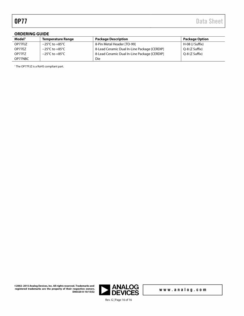
ORDERING GUIDE Model1 Temperature Range Package Description Package Option OP77FJZ −25°C to +85°C 8-Pin Metal Header [TO-99] H-08 (J Suffix) OP77EZ −25°C to +85°C 8-Lead Ceramic Dual In-Line Package [CERDIP] Q-8 (Z Suffix) OP77FZ −25°C to +85°C 8-Lead Ceramic Dual In-Line Package [CERDIP] Q-8 (Z Suffix) OP77NBC Die 1 The OP77FJZ is a RoHS compliant part.
©2002–2015 Analog Devices, Inc. All rights reserved. Trademarks and registered trademarks are the property of their respective owners. D00320-0-10/15(G)


![Unigear Ma_en 1vlm000363 Rev[1].g](https://static.fdocuments.us/doc/165x107/551fa676497959335b8b50af/unigear-maen-1vlm000363-rev1g.jpg)