ONET1131EC Externally Modulated Laser Driver With ...
50
Copyright © 2016, Texas Instruments Incorporated Optical Module Backplane Optical Fiber TOSA CDR LD EQ Laser + Optical MUX ONET1131EC TIA PD + Optical DEMUX PA CDR Optical Transceiver ROSA MUX Data Clock Clock n-bit parallel data DE- MUX Data Clock Clock n-bit parallel data Product Folder Sample & Buy Technical Documents Tools & Software Support & Community An IMPORTANT NOTICE at the end of this data sheet addresses availability, warranty, changes, use in safety-critical applications, intellectual property matters and other important disclaimers. PRODUCTION DATA. ONET1131EC SLLSEQ6A – SEPTEMBER 2016 – REVISED SEPTEMBER 2016 ONET1131EC Externally Modulated Laser Driver With Integrated Clock and Data Recovery (CDR) 1 1 Features 1• Modulator Driver with Minimum Output Amplitude up to 2 Vpp Single-Ended and Bias Current up to 150 mA Source • Supports Externally Modulated Lasers Including the Electro-Absorption Modulator Lasers (EML) and the Mach-Zahnder Modulator (MZM) Based lasers • Integrated CDR with 9.80 – 11.7 Gbps Reference- Free Operation • Two-Wire Digital Interface with Integrated DACs and ADC for Control and Diagnostic Management • Output Polarity Select • Programmable Jitter Transfer Bandwidth to Adjust CDR Bandwidth • CDR Bypass Mode for Low Data Rate Operation • Automatic Power Control (APC) Loop with Selectable Monitor PD Range • Programmable Transmit Input Equalizer • Transmitter Cross-Point Adjust and De-Emphasis • Includes Laser Safety Features • Power Supply Monitor and Temperature Sensor • Single 2.5 V Supply • –40°C to 100°C Operation • Surface Mount 4 mm x 4 mm 32-Pin QFN Package with 0.4 mm Pitch 2 Applications • 10-Gbps Passive Optical Network (PON), Optical Line Terminal (OLT) Transceivers for FTTx deployment • XFP and SFP+ 10-Gbps SONET OC-192 Optical Transceivers • XFP and SFP+ 10GBASE-ER/ZR Optical Transceivers • 8x and 10x Fibre Channel Optical Transmitters 3 Description The ONET1131EC is a 2.5-V EML modulator driver with transmit clock and data recovery (CDR) designed to operate between 9.8 Gbps and 11.7 Gbps without the need for a reference clock. CDR bypass mode can be used for operation at lower data rates and a two-wire serial interface allows digital control of features like output polarity select and input equalization. The transmit path consists of an adjustable input equalizer for equalization of up to 300 mm (12 inches) of microstrip or stripline transmission line of FR4 printed circuit boards, a multi-rate CDR and an output modulator driver. Output waveform control, in the form of cross-point adjustment and de- emphasis, is available to improve the optical eye mask margin. The device provides bias current for the laser and an integrated automatic power control (APC) loop to compensate for variations in average optical power over voltage, temperature and time. The ONET1131EC contains internal analog to digital and digital to analog converters to support transceiver management and eliminate the need for special purpose microcontrollers. Device Information (1) PART NUMBER PACKAGE BODY SIZE (NOM) ONET1131EC VQFN (32) 4.00 mm x 4.00 mm (1) For all available packages, see the orderable addendum at the end of the data sheet. Simplified Block Diagram
Transcript of ONET1131EC Externally Modulated Laser Driver With ...

Copyright © 2016, Texas Instruments Incorporated
Optical Module
Ba
ckp
lan
e
Optical Fiber
TOSA
CDR LD EQLaser + Optical
MUX
ONET1131EC
TIAPD + Optical
DEMUXPACDR
Optical TransceiverROSA
MUX
Data
ClockClock
n-bit
parallel
data
DE-
MUX
Data
ClockClock
n-bit
parallel
data
Product
Folder
Sample &Buy
Technical
Documents
Tools &
Software
Support &Community
An IMPORTANT NOTICE at the end of this data sheet addresses availability, warranty, changes, use in safety-critical applications,intellectual property matters and other important disclaimers. PRODUCTION DATA.
ONET1131ECSLLSEQ6A –SEPTEMBER 2016–REVISED SEPTEMBER 2016
ONET1131EC Externally Modulated Laser Driver With IntegratedClock and Data Recovery (CDR)
1
1 Features1• Modulator Driver with Minimum Output Amplitude
up to 2 Vpp Single-Ended and Bias Current up to150 mA Source
• Supports Externally Modulated Lasers Includingthe Electro-Absorption Modulator Lasers (EML)and the Mach-Zahnder Modulator (MZM) Basedlasers
• Integrated CDR with 9.80 – 11.7 Gbps Reference-Free Operation
• Two-Wire Digital Interface with Integrated DACsand ADC for Control and Diagnostic Management
• Output Polarity Select• Programmable Jitter Transfer Bandwidth to Adjust
CDR Bandwidth• CDR Bypass Mode for Low Data Rate Operation• Automatic Power Control (APC) Loop with
Selectable Monitor PD Range• Programmable Transmit Input Equalizer• Transmitter Cross-Point Adjust and De-Emphasis• Includes Laser Safety Features• Power Supply Monitor and Temperature Sensor• Single 2.5 V Supply• –40°C to 100°C Operation• Surface Mount 4 mm x 4 mm 32-Pin QFN
Package with 0.4 mm Pitch
2 Applications• 10-Gbps Passive Optical Network (PON), Optical
Line Terminal (OLT) Transceivers for FTTxdeployment
• XFP and SFP+ 10-Gbps SONET OC-192 OpticalTransceivers
• XFP and SFP+ 10GBASE-ER/ZR OpticalTransceivers
• 8x and 10x Fibre Channel Optical Transmitters
3 DescriptionThe ONET1131EC is a 2.5-V EML modulator driverwith transmit clock and data recovery (CDR)designed to operate between 9.8 Gbps and 11.7Gbps without the need for a reference clock. CDRbypass mode can be used for operation at lower datarates and a two-wire serial interface allows digitalcontrol of features like output polarity select and inputequalization.
The transmit path consists of an adjustable inputequalizer for equalization of up to 300 mm(12 inches) of microstrip or stripline transmission lineof FR4 printed circuit boards, a multi-rate CDR andan output modulator driver. Output waveform control,in the form of cross-point adjustment and de-emphasis, is available to improve the optical eyemask margin. The device provides bias current forthe laser and an integrated automatic power control(APC) loop to compensate for variations in averageoptical power over voltage, temperature and time.
The ONET1131EC contains internal analog to digitaland digital to analog converters to support transceivermanagement and eliminate the need for specialpurpose microcontrollers.
Device Information(1)
PART NUMBER PACKAGE BODY SIZE (NOM)ONET1131EC VQFN (32) 4.00 mm x 4.00 mm
(1) For all available packages, see the orderable addendum atthe end of the data sheet.
Simplified Block Diagram

2
ONET1131ECSLLSEQ6A –SEPTEMBER 2016–REVISED SEPTEMBER 2016 www.ti.com
Product Folder Links: ONET1131EC
Submit Documentation Feedback Copyright © 2016, Texas Instruments Incorporated
Table of Contents1 Features .................................................................. 12 Applications ........................................................... 13 Description ............................................................. 14 Revision History..................................................... 25 Pin Configuration and Function ........................... 36 Specifications......................................................... 5
6.1 Absolute Maximum Ratings ..................................... 56.2 ESD Ratings ............................................................ 56.3 Recommended Operating Conditions....................... 56.4 Thermal Information .................................................. 66.5 DC Electrical Characteristics .................................... 66.6 AC Electrical Characteristics..................................... 86.7 Timing Requirements ................................................ 96.8 Timing Diagram Definitions..................................... 106.9 Typical Characteristics ............................................ 11
7 Detailed Description ............................................ 157.1 Overview ................................................................. 157.2 Functional Block Diagram ....................................... 15
7.3 Feature Description................................................. 167.4 Device Functional Modes........................................ 217.5 Programming .......................................................... 217.6 Register Mapping .................................................... 22
8 Application Information and Implementations . 358.1 Application Information............................................ 358.2 Typical Application, Transmitter Differential Mode.. 35
9 Power Supply Recommendations ...................... 3910 Layout................................................................... 40
10.1 Layout Guidelines ................................................. 4010.2 Layout Example .................................................... 40
11 Device and Documentation Support ................. 4111.1 Receiving Notification of Documentation Updates 4111.2 Community Resources.......................................... 4111.3 Trademarks ........................................................... 4111.4 Electrostatic Discharge Caution............................ 4111.5 Glossary ................................................................ 41
12 Mechanical, Packaging, and OrderableInformation ........................................................... 41
4 Revision History
Changes from Original (September 2016) to Revision A Page
• Deleted sentence "however, this function..." from the second paragraph of the CDR section ............................................ 16• Deleted the RX Registers section from Register Mapping .................................................................................................. 23• Deleted sentence "RX_CDRBP must be set to 1 for this function to operate." From Bit 3 of Table 6 ................................ 25• Deleted the RX Registers 42 (offset = 0000 0000 [reset = 0h] section from Register Mapping ......................................... 33

1
3
2
4
9 1110 12
21
22
23
24
29303132
BIA
S
25262728
MONB
DIS
5
7
6
8
LOL
DIN-
DIN+
17
18
19
20
13 1514 16
GND
LF
PD
NC
VC
C
MONP
FLT
OU
T+
OU
T-
VC
CV
CC
VC
C
VD
D
GND
GND
SDA
SCK
GND
AM
P
COMP
NC
NC
NC
NC
NC
NC
3
ONET1131ECwww.ti.com SLLSEQ6A –SEPTEMBER 2016–REVISED SEPTEMBER 2016
Product Folder Links: ONET1131EC
Submit Documentation FeedbackCopyright © 2016, Texas Instruments Incorporated
5 Pin Configuration and FunctionThe ONET1131EC is packaged in a small footprint 4 mm x 4 mm 32 pin RoHS compliant QFN package with alead pitch of 0.4 mm.
RSM Package32 PIN VQFN(Top View)
Pin FunctionsNUMBER NAME Type DESCRIPTION
LOL 1 Digital-outLoss of lock indicator. High level indicates the transmitter CDR is out of lock. Opendrain output. Requires an external 4.7 kΩ to 10 kΩ pull-up resistor to VCC for properoperation. This pin is 3.3 V tolerant.
MONB 2 Analog-out Bias current monitor.GND 3, 6, 19, 22 Supply Circuit ground.
DIN+ 4 Analog-in Non-inverted transmitter data input. On-chip differentially 100 Ω terminated to TXIN–.Must be AC coupled.
DIN– 5 Analog-in Inverted transmitter data input. On-chip differentially 100 Ω terminated to TXIN+. Mustbe AC coupled.
PD 7 Analog Photodiode input. Pin can source or sink current dependent on register setting.MONP 8 Analog-out Photodiode current monitor.LF 9 Analog-in Transmitter loop filter capacitor.BIAS 10 Analog Sinks or sources the bias current for the laser in both APC and open loop modes.VCC 11, 14, 27, 30 Supply 2.5 V ± 5% supply.
OUT– 12 CML-out Inverted transmitter data output. Internally terminated in single-ended operationmode.
OUT+ 13 CML-out Non-Inverted transmitter data output.VDD 15 Supply 2.5 V ± 5% supply for the digital circuitry.
AMP 16 Analog-in Output amplitude control. Output amplitude can be adjusted by applying a voltage of0 to 2 V to this pin. Leave open when not used.

4
ONET1131ECSLLSEQ6A –SEPTEMBER 2016–REVISED SEPTEMBER 2016 www.ti.com
Product Folder Links: ONET1131EC
Submit Documentation Feedback Copyright © 2016, Texas Instruments Incorporated
Pin Functions (continued)NUMBER NAME Type DESCRIPTION
SDA 17 Digital-in/out 2-wire interface serial data input. Requires an external 4.7-kΩ to10-kΩ pull-up resistorto VCC. This pin is 3.3-V tolerant.
SCK 18 Digital-in 2-wire interface serial clock input. Requires an external 4.7-kΩ to10-kΩ pull-upresistor to VCC. This pin is 3.3-V tolerant.
NC 20, 21, 24, 25,26, 28, 29 Do not connect
COMP 23 Analog Compensation pin used to control the bandwidth of the APC loop. Connect a 0.01-µFcapacitor to ground.
FLT 31 Digital-outTransmitter fault detection flag. High level indicates that a fault has occurred. Opendrain output. Requires an external 4.7 kΩ to 10 kΩ pull-up resistor to VCC for properoperation. This pin is 3.3-V tolerant.
DIS 32 Digital-in
Disables the bias current when set to high state. Includes a 250-kΩ pull-up resistor toVCC. Requires an external 4.7 kΩ to 10 kΩ pull-up resistor to VCC for properoperation Toggle to reset a fault condition. This is an ORed function with theTXBIASEN bit (bit 2 in register 1). This pin is 3.3-V tolerant.

5
ONET1131ECwww.ti.com SLLSEQ6A –SEPTEMBER 2016–REVISED SEPTEMBER 2016
Product Folder Links: ONET1131EC
Submit Documentation FeedbackCopyright © 2016, Texas Instruments Incorporated
(1) Stresses beyond those listed under “absolute maximum ratings” may cause permanent damage to the device. These are stress ratingsonly and functional operation of the device at these or any other conditions beyond those indicated under “recommended operatingconditions” is not implied. Exposure to absolute–maximum–rated conditions for extended periods may affect device reliability.
(2) All voltage values are with respect to network ground terminal.
6 Specifications
6.1 Absolute Maximum Ratings (1) (2)
over operating free-air temperature range (unless otherwise noted)MIN MAX UNIT
Supply voltage at VCC, VDD –0.5 3 V
Voltageat 3.3-V tolerant pins LOL, SDA, SCK, FLT, DIS –0.5 3.6 Vat all other pins MONB, DIN+, DIN–, PD, MONP, LF, BIAS,OUT–, OUT+, AMP, COMP –0.5 3 V
Maximum current at transmitter input pins DIN+, DIN– 10 mAMaximum current at transmitter outputpins OUT+, OUT– 125 mA
Maximum junction temperature, TJ 125 °CStorage temperature, Tstg –65 150 °C
(1) JEDEC document JEP155 states that 500-V HBM allows safe manufacturing with a standard ESD control process.
6.2 ESD RatingsVALUE UNIT
V(ESD)Electrostaticdischarge Human-body model (HBM), per ANSI/ESDA/JEDEC JS-001 (1) ±2000 V
6.3 Recommended Operating Conditionsover operating free-air temperature range (unless otherwise noted)
MIN TYP MAX UNITVCC Supply Voltage 2.37 2.5 2.63 VVIH Digital input high voltage
DIS, SCK, SDA, 3.3-V tolerant IOs2 V
VIL Digital input low voltage 0.8 V
Photodiode current rangeControl bit TXPDRNG = 1x, step size = 3 µA 3080
µAControl bit TXPDRNG = 01, step size = 1.5 µA 1540Control bit TXPDRNG = 00, step size = 0.75 µA 770
Serial Data rateTXCDR_DIS = 0 9.8 11.7
GbpsTXCDR_DIS = 1 1 11.7
VAMP Amplitude control input voltage range 0 2 VtR(IN) Input rise time 20%–80% 30 45 pstF(IN) Input fall time 20%–80% 30 45 psTC Temperature at thermal pad –40 100 °C
6
ONET1131ECSLLSEQ6A –SEPTEMBER 2016–REVISED SEPTEMBER 2016 www.ti.com
Product Folder Links: ONET1131EC
Submit Documentation Feedback Copyright © 2016, Texas Instruments Incorporated
(1) For more information about traditional and new thermal metrics, see the Semiconductor and IC Package Thermal Metrics applicationreport.
6.4 Thermal Information
THERMAL METRIC (1) RSM (VQFN)UNIT
32 PINSRθJA Junction-to-ambient thermal resistance 37.2 °C/WRθJCtop Junction-to-case (top) thermal resistance 30.1 °C/WRθJB Junction-to-board thermal resistance 7.8 °C/WψJT Junction-to-top characterization parameter 0.4 °C/WψJB Junction-to-board characterization parameter 7.6 °C/WRθJCbot Junction-to-case (bottom) thermal resistance 2.4 °C/W
(1) The bias current can be set below the specified minimum according to the corresponding register setting; however, in closed loopoperation settings below the specified value may trigger a fault.
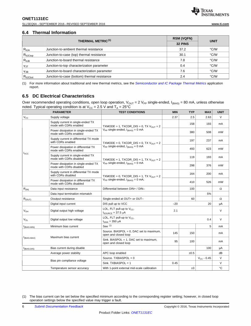
6.5 DC Electrical CharacteristicsOver recommended operating conditions, open loop operation, VOUT = 2 VPP single-ended, I(BIAS) = 80 mA, unless otherwisenoted. Typical operating condition is at VCC = 2.5 V and TA = 25°C
PARAMETER TEST CONDITIONS MIN TYP MAX UNIT
VCC Supply voltage 2.37 2.5 2.63 V
IVCC
Supply current in single-ended TXmode with CDRs enabled TXMODE = 1, TXCDR_DIS = 0, TX VOUT = 2
VPP single-ended, I(BIAS) = 0 mA
158 193 mA
Power dissipation in single-ended TXmode with CDRs enabled 380 508 mW
Supply current in differential TX modewith CDRs enabled TXMODE = 0, TXCDR_DIS = 0, TX VOUT = 2
VPP single-ended, I(BIAS) = 0 mA
197 237 mA
Power dissipation in differential TXmode with CDRs enabled 493 623 mW
Supply current in single-ended TXmode with CDRs disabled TXMODE = 1, TXCDR_DIS = 1, TX VOUT = 2
VPP single-ended, I(BIAS) = 0 mA
119 193 mA
Power dissipation in single-ended TXmode with CDRs disabled 298 376 mW
Supply current in differential TX modewith CDRs disabled TXMODE = 0, TXCDR_DIS = 1, TX VOUT = 2
VPP single-ended, I(BIAS) = 0 mA;
164 200 mA
Power dissipation in differential TXmode with CDRs disabled 410 526 mW
R(IN) Data input resistance Differential between DIN+ / DIN– 100 Ω
Data input termination mismatch 5%
R(OUT) Ooutput resistance Single-ended at OUT+ or OUT– 60 Ω
Digital input current DIS pull up to VCC –20 20 µA
VOH Digital output high voltage LOL, FLT pull-up to VCC,ISOURCE = 37.5 μA 2.1 V
VOL Digital output low voltage LOL, FLT pull-up to VCC,ISINK = 350 μA 0.4 V
I(BIAS-MIN) Minimum bias current See (1) 5 mA
I(BIAS-MAX) Maximum bias current
Source. BIASPOL = 0, DAC set to maximum,open and closed loop 145 150 mA
Sink. BIASPOL = 1, DAC set to maximum,open and closed loop 95 100 mA
I(BIAS-DIS) Bias current during disable 100 µA
Average power stability APC loop enabled ±0.5 dB
Bias pin compliance voltageSource. TXBIASPOL = 0 VCC - 0.45 V
Sink. TXBIASPOL = 1 0.45 V
Temperature sensor accuracy With 1-point external mid-scale calibration ±3 °C

7
ONET1131ECwww.ti.com SLLSEQ6A –SEPTEMBER 2016–REVISED SEPTEMBER 2016
Product Folder Links: ONET1131EC
Submit Documentation FeedbackCopyright © 2016, Texas Instruments Incorporated
DC Electrical Characteristics (continued)Over recommended operating conditions, open loop operation, VOUT = 2 VPP single-ended, I(BIAS) = 80 mA, unless otherwisenoted. Typical operating condition is at VCC = 2.5 V and TA = 25°C
PARAMETER TEST CONDITIONS MIN TYP MAX UNIT
(2) Specified by design over process, supply and temperature variation
V(PD)
Photodiode reverse bias voltage APC active, I(PD) = 1500 μA 1.3 2.3 V
Photodiode fault current level Percent of target I(PD)(2) 150%
Photodiode current monitor ratio
I(MONP) / I(PD) with control bit PDRNG = 1X 10% 12.5% 15%
I(MONP) / I(PD) with control bit PDRNG = 01 20% 25% 30%
I(MONP) / I(PD) with control bit TXPDRNG = 00 40% 50% 60%
Monitor diode DMI accuracy With external mid-scale calibration –15% 15%
Bias current monitor ratio I(MONB) / I(BIAS) (nominal 1/100 = 1%), V(MONB)< 1.5V 0.9% 1% 1..1%
Bias current DMI accuracy I(BIAS) ≥ 20 mA –15% 15%
Power supply monitor accuracy With external mid-scale calibration –2% 2%
VCC(RST) VCC reset threshold voltage VCC voltage level which triggers power-onreset 1.8 2.1 V
VCC(RSTHYS) VCC reset threshold voltage hysteresis 100 mV
V(MONB-FLT) Fault voltage at MONB TXFLTEN = 1, TXDMONB = 0, Fault occursif voltage at MONB exceeds this value 1.15 1.2 1.25 V
V(MONP-FLT) Fault voltage at MONPTXFLTEN = 1, TXMONPFLT = 1, TXDMONP= 0, Fault occurs if voltage at MONPexceeds this value
1.15 1.2 1.25 V

8
ONET1131ECSLLSEQ6A –SEPTEMBER 2016–REVISED SEPTEMBER 2016 www.ti.com
Product Folder Links: ONET1131EC
Submit Documentation Feedback Copyright © 2016, Texas Instruments Incorporated
6.6 AC Electrical CharacteristicsOver recommended operating conditions, open loop operation, VOUT = 2 VPP single-ended, I(BIAS) = 80 mA unless otherwisenoted. Typical operating condition is at VCC = 2.5 V and TA = 25°C
PARAMETER TEST CONDITIONS MIN TYP MAX UNIT
TX INPUT SPECIFICATIONS
CDR lock range CPRI, Ethernet, SONET, Fibre Channel 9.80 11.7 Gbps
SDD11 Differential input return loss
0.05 GHz < f ≤ 0.1 GHz 20
dB0.1 GHz < f ≤ 5.5 GHz 12 15
5.5 GHz < f < 12 GHz 8
SDD11 Differential to common mode conversion 0.1 GHz < f < 12 GHz 10 15 dB
SDD11 Common mode input return loss 0.1 GHz < f < 12 GHz 3 dB
Input AC common mode voltage tolerance 15 mV
Total Non-DDJ Total jitter less ISI 0.45 UIPP
T(JTX) Total Jitter 0.65 UIPP
S(JTX) Sinusoidal Jitter Tolerance With addition of input jitter, See Figure 1 UIPP
VIN Differential input voltage swing 100 1000 mVPP
EQ(boost) EQ high freq boost Maximum setting; 7 GHz 6 9 dB
TX OUTPUT SPECIFICATIONS
Differential output return loss 0.01 GHz < f < 12 GHz 12 dB
VO(MIN) Minimum output amplitude AC Coupled Outputs, 50-Ω single-ended load 0.5 VPP
TX OUTPUT SPECIFICATIONS in SINGLE-ENDED MODE of OPERATION (TXMODE = 1)
VO(MAX) Maximum output amplitude AC Coupled Outputs, 50-Ω load, single-ended 2 VPP
Output amplitude stability AC Coupled Outputs, 50-Ω load, single-ended 230 mVPP
High Cross Point Control Range 50-Ω load, single-ended 70% 75%
Low Cross Point Control Range 50-Ω load, single-ended 35% 40%
Cross Point Stability 50-Ω load, single-ended -5 5 pp
Output de-emphasisTXDEADJ[0..3] = 1111, TXPKSEL = 0 5
dBTXDEADJ[0..3] = 1111, TXPKSEL = 1 6
TX OUTPUT SPECIFICATIONS in DIFFERENTIAL MODE of OPERATION (TXMODE = 0)
VO(MAX) Maximum output amplitude AC Coupled Outputs, 100-Ω differential load 3.6 VPP
Output amplitude stability AC Coupled Outputs, 100-Ω differential load 230 mVPP
High Cross Point Control Range 100-Ω differential load 65% 75%
Low Cross Point Control Range 100-Ω differential load 35% 40%
Cross Point Stability 100-Ω differential load –5 5 pp
Output de-emphasisTXDEADJ[0..3] = 1111, TXPKSEL = 0 5
dBTXDEADJ[0..3] = 1111, TXPKSEL = 1 6
CDR SPECIFICATIONS
BW(TX) Jitter Transfer Bandwidth 9.95 Gbps, PRBS31 8 MHz
J(PTX) Jitter Peaking > 120 kHz 1 dB
JGEN(rms) Random RMS jitter generation Clock pattern, 50 kHz to 80 MHz 6 mUIrms
JGEN(PP) Total jitter generation Clock pattern, 50 kHz to 80 MHz, BER = 10-12 60 mUIPP

9
ONET1131ECwww.ti.com SLLSEQ6A –SEPTEMBER 2016–REVISED SEPTEMBER 2016
Product Folder Links: ONET1131EC
Submit Documentation FeedbackCopyright © 2016, Texas Instruments Incorporated
6.7 Timing RequirementsOver recommended operating conditions, typical operating condition is at VCC = 2.5 V and TA = 25°C
MIN TYP MAX UNIT
t(APC) APC time constant CAPC 0.01 µF, IPD = 500 µA, PD coupling ratio CR = 150,PDRNG = 01 50 µs
t(INIT1) Power-on to initialize Power-on to registers ready to be loaded 0.2 1 ms
t(INIT2) Initialize to transmit Register load STOP command to part ready to transmit valid data 2 ms
t(OFF) Transmitter disable time Rising edge of DIS to I(BIAS) ≤ 0.1 × I(BIAS-NOMINAL) 1 5 µs
t(ON) Disable negate time Falling edge of DIS to I(BIAS) ≥ 0.9 × I(BIAS-NOMINAL) 1 ms
t(RESET) DIS pulse width Time DIS must held high to reset part 100 ns
t(FAULT) Fault assert time Time from fault condition to FLT high 50 µs
OUTPUT SPECIFICATIONS in SINGLE-ENDED MODE of OPERATION (TXMODE = 1)
tR(OUTTX) Output rise time 20% - 80%, AC Coupled Outputs, 50-Ω load, single-ended 30 42 ps
tF(OUTTX) Output fall time 20% - 80%, AC Coupled Outputs, 50-Ω load, single-ended 30 42 ps
ISI(TX) Intersymbol interference
TXEQ_DIS = 1, 11.3 Gbps, PRBS9 pattern, 150-mVpp,600-mVpp, 1200-mVpp differential input voltage 4 12
psTXEQ_DIS = 0, 11.3 Gbps, PRBS9 pattern, 150-mVpp,600-mVpp, 1200-mVpp differential input voltage, maximumequalization with 18-inch transmission line at the input.
7
R(JTX)Serial data output randomjitter 0.4 0.75 psRMS
Output de-emphasis widthTXPKSEL = 0 28
psTXPKSEL = 1 35
OUTPUT SPECIFICATIONS in DIFFERENTIAL MODE of OPERATION (TXMODE = 0)
tR(OUTTX) Output rise time 20%–80%, AC Coupled Outputs, 100-Ω differential load 30 42 ps
tF(OUTTX) Output fall time 20%–80%, AC Coupled Outputs, 100-Ω differential load 30 42 ps
ISI(TX) Intersymbol interference
TXEQ_DIS = 1, 11.3 Gbps, PRBS9 pattern, 150-mVpp,600-mVpp, 1200-mVpp differential input voltage 4 10
psTXEQ_DIS = 0, 11.3 Gbps, PRBS9 pattern, 150-mVpp,600-mVpp, 1200-mVpp differential input voltage, maximumequalization with 18-inch transmission line at the input.
7
R(JTX)Serial data output randomjitter 0.4 0.75 psRMS
Output Peaking WidthTXPKSEL = 0 28
psTXPKSEL = 1 35
CDR SPECIFICATIONS
t(Lock,TX) CDR Acquisition time 2 ms
LOL assert time 500 μs

tBUF±
tHDSTA
tr
tLOW
tHDDAT
tHIGH
tf
tSUDAT
tSUSTA
tHDSTA
tSUSTO
P S S P
SDA
SCK
10
ONET1131ECSLLSEQ6A –SEPTEMBER 2016–REVISED SEPTEMBER 2016 www.ti.com
Product Folder Links: ONET1131EC
Submit Documentation Feedback Copyright © 2016, Texas Instruments Incorporated
Figure 1. Input Sinusoidal Jitter Tolerance (INF-8077i Rev. 4.5 XFP MSA)
Figure 2. 2-Wire Interface Diagram
6.8 Timing Diagram DefinitionsMIN TYP MAX UNIT
fSCK SCK clock frequency 400 kHztBUF Bus free time between START and STOP conditions 1.3 µstHDSTA Hold time after repeated START condition. After this period, the first
clock pulse is generated0.6 µs
tLOW Low period of the SCK clock 1.3 µstHIGH High period of the SCK clock 0.6 µstSUSTA Setup time for a repeated START condition 0.6 µstHDDAT Data HOLD time 0 µstSUDAT Data setup time 100 nstR Rise time of both SDA and SCK signals 300 nstF Fall time of both SDA and SCK signals 300 nstSUSTO Setup time for STOP condition 0.6 µs

Modulation Current Register Setting (Decimal)
Ran
dom
Jitt
er (
psrm
s)
0 20 40 60 80 100 120 140 160 180 200 2200
0.1
0.2
0.3
0.4
0.5
0.6
0.7
0.8
0.9
1
D014Free-Air Temperature (°C)
Ran
dom
Jitt
er (
psrm
s)
-40 -20 0 20 40 60 80 1000
0.1
0.2
0.3
0.4
0.5
0.6
0.7
0.8
0.9
1
D015
Free-Air Temperature (°C)
ISI (
psP
P)
-40 -20 0 20 40 60 80 1000
2
4
6
8
D012Free-Air Temperature (°C)
ISI (
psP
P)
-40 -20 0 20 40 60 80 1000
2
4
6
8
D013
TXMOD Register 12 Setting (Decimal)
ISI (
psP
P)
0 20 40 60 80 100 120 140 160 180 2000
1
2
3
4
5
6
7
8
D010TXMOD Register 12 Setting (Decimal)
ISI (
psP
P)
0 20 40 60 80 100 120 140 160 180 2000
1
2
3
4
5
6
7
8
D011
11
ONET1131ECwww.ti.com SLLSEQ6A –SEPTEMBER 2016–REVISED SEPTEMBER 2016
Product Folder Links: ONET1131EC
Submit Documentation FeedbackCopyright © 2016, Texas Instruments Incorporated
6.9 Typical CharacteristicsTypical operating condition is at VCC = 2.5 V, TA = 25°C, VOUT = 2 VPP Single-ended, DIN = 600 mVPP differential, CDRenabled (unless otherwise noted).
TXMODE = 0
Figure 3. Deterministic Jitter vs Modulation Current
TXMODE = 1
Figure 4. Deterministic Jitter vs Modulation Current
TXMODE = 0
Figure 5. Deterministic Jitter vs Temperature
TXMODE = 1
Figure 6. Deterministic Jitter vs Temperature
TXMODE = 1
Figure 7. Random Jitter vs Modulation Current
TXMODE = 1
Figure 8. Random Jitter vs Temperature

Bias Current (mA)
Bia
s M
onito
r C
urre
nt (
mA
)
0 20 40 60 80 100 120 140 160 1800
0.2
0.4
0.6
0.8
1
1.2
1.4
1.6
1.8
D020Photodiode Current (mA)
Pho
todi
ode
Mon
itor
Cur
rent
(m
A)
0 0.1 0.2 0.3 0.4 0.5 0.6 0.7 0.8 0.9 10
0.1
0.2
0.3
0.4
0.5
D021
TXBIAS Register 15 and 16 Setting (Decimal)
Sou
rce
OL
Bia
s C
urre
nt (
mA
)
0 200 400 600 800 1000 12000
20
40
60
80
100
120
140
160
180
D018TXBIAS Register 15 and 16 Setting (Decimal)
Sin
k O
L B
ias
Cur
rent
(m
A)
0 200 400 600 800 1000 12000
20
40
60
80
100
120
140
160
180
D019
TXMOD Register 12 Setting - Decimal
Tra
nsiti
on T
ime
(ps)
0 20 40 60 80 100 120 140 160 180 200 2200
5
10
15
20
25
30
35
40
D016
Rise TimeFall Time
Free-Air Temperature (°C)
Tra
nsiti
on T
ime
(ps)
-40 -20 0 20 40 60 80 1000
5
10
15
20
25
30
35
D017
Rise TimeFall Time
12
ONET1131ECSLLSEQ6A –SEPTEMBER 2016–REVISED SEPTEMBER 2016 www.ti.com
Product Folder Links: ONET1131EC
Submit Documentation Feedback Copyright © 2016, Texas Instruments Incorporated
Typical Characteristics (continued)Typical operating condition is at VCC = 2.5 V, TA = 25°C, VOUT = 2 VPP Single-ended, DIN = 600 mVPP differential, CDRenabled (unless otherwise noted).
TXMODE = 1
Figure 9. Rise-Time and Fall-Time vs Modulation Current
TXMODE = 1
Figure 10. Rise-Time and Fall-Time vs Temperature
Figure 11. Source Bias Current in Open Loop Mode vs BiasRegister Setting
Figure 12. Sink Bias Current in Open Loop Mode vs BiasRegister Setting
Figure 13. Bias-Monitor Current I(MONB) vs Bias Current
TXPDRNG[0..1] = 00
Figure 14. Photodiode-Monitor Current I(MONP) vs PD Current

TXBMF Register 17 Setting (Decimal)
Bia
s F
ault
Cur
rent
(m
A)
0 50 100 150 200 250 3000
20
40
60
80
100
120
140
160
180
D026TXPMF Register 18 Setting (Decimal)
PD
Fau
lt C
urre
nt (
mA
)
0 50 100 150 200 250 3000
0.2
0.4
0.6
0.8
1
1.2
D027
Free Air Temperature (°C
Sup
ply
Cur
rent
(m
A)
-40 -20 0 20 40 60 80 100220
230
240
250
260
270
280
290
300
D024Free Air Temperature (°C)
Sup
ply
Cur
rent
(m
A)
-40 -20 0 20 40 60 80 100180
190
200
210
220
230
240
250
260
D025
TXMOD Register 12 Setting (Decimal)
Diff
eren
tial O
utpu
t Vol
tage
(V
)
0 20 40 60 80 100 120 140 160 180 200 2200
0.5
1
1.5
2
2.5
3
3.5
4
4.5
D022TXMOD Register 12 Setting (Decimal)
Diff
eren
tial O
utpu
t Vol
tage
(V
)
0 20 40 60 80 100 120 140 160 180 200 2200
0.5
1
1.5
2
2.5
D023
13
ONET1131ECwww.ti.com SLLSEQ6A –SEPTEMBER 2016–REVISED SEPTEMBER 2016
Product Folder Links: ONET1131EC
Submit Documentation FeedbackCopyright © 2016, Texas Instruments Incorporated
Typical Characteristics (continued)Typical operating condition is at VCC = 2.5 V, TA = 25°C, VOUT = 2 VPP Single-ended, DIN = 600 mVPP differential, CDRenabled (unless otherwise noted).
TXMODE = 0
Figure 15. Output Voltage vs Modulation Current
TXMODE = 1
Figure 16. Output Voltage vs Modulation Current
TXMODE = 0 Bias Current = 0
Figure 17. Supply Current vs Temperature
TXMODE = 1 Bias Current = 0
Figure 18. Supply Current vs Temperature
Figure 19. Bias Current Monitor Fault vs TXBMF RegisterSetting
Figure 20. Photodiode Current Monitor Fault vs TXPMFRegister Setting

14
ONET1131ECSLLSEQ6A –SEPTEMBER 2016–REVISED SEPTEMBER 2016 www.ti.com
Product Folder Links: ONET1131EC
Submit Documentation Feedback Copyright © 2016, Texas Instruments Incorporated
Typical Characteristics (continued)Typical operating condition is at VCC = 2.5 V, TA = 25°C, VOUT = 2 VPP Single-ended, DIN = 600 mVPP differential, CDRenabled (unless otherwise noted).
TXMODE = 0 15 ps/Div
Figure 21. Eye-Diagram at 11.3 Gbps
TXMODE = 1 15 ps/Div
Figure 22. Eye-Diagram at 11.3 Gbps

DIS
OUT+
OUT-
DIN+
DIN-
SCK
SDA
BIAS
PD
Modulator
Driver
FLT
EqualizerReferenceless
CDR and Retimer
100
Band-Gap, Analog
References, Power Supply
Monitor & Temperature
Sensor
Modulation
and Bias
Current
Generator &
APC
MONB
MONP
FLT
PD
BIAS
Analog to
Digital
Conversion
TS
PSM
2-Wire Interface &
Control Logic
LOL
CDR_CTRL
LF
MONB
MONP
LOL
Power-On
Reset
EEPROM
VCC
VDD
MONB
MONP
COMPCOMP
AMPAMP
60 60
Copyright © 2016, Texas Instruments Incorporated
15
ONET1131ECwww.ti.com SLLSEQ6A –SEPTEMBER 2016–REVISED SEPTEMBER 2016
Product Folder Links: ONET1131EC
Submit Documentation FeedbackCopyright © 2016, Texas Instruments Incorporated
7 Detailed Description
7.1 OverviewA simplified block diagram of the ONET1131EC is shown in Functional Block Diagram.
The ONET1131EC consists of a transmitter path, an analog reference block, an analog to digital converter, and a2-wire serial interface and control logic block with power-on reset.
The transmit path consists of an adjustable input equalizer, a multi-rate CDR and an output modulator driver. Theoutput driver provides a differential output voltage but can be operated in a single-ended mode to reduce thepower consumption. Output waveform control, in the form of cross-point adjustment and de-emphasis areavailable to improve the optical eye mask margin. Bias current for the laser is provided and an integratedautomatic power control (APC) loop to compensate for variations in average optical power over voltage,temperature and time is included.
The ONET1131EC contains an analog to digital converter to support transceiver digital diagnostics and canreport the supply voltage, laser bias current, laser photodiode current and internal temperature.
The 2-wire serial interface is used to control the operation of the device and read the status of the controlregisters.
7.2 Functional Block Diagram

16
ONET1131ECSLLSEQ6A –SEPTEMBER 2016–REVISED SEPTEMBER 2016 www.ti.com
Product Folder Links: ONET1131EC
Submit Documentation Feedback Copyright © 2016, Texas Instruments Incorporated
7.3 Feature Description
7.3.1 EqualizerThe data signal is applied to an input equalizer by means of the input signal pins DIN+ / DIN–, which provide on-chip differential 100-Ω line termination. The equalizer is enabled by default and can be disabled by setting thetransmitter equalizer disable bit TXEQ_DIS = 1 (bit 1 of register 10). Equalization of up to 300 mm (12 inches) ofmicrostrip or stripline transmission line on FR4 printed circuit boards can be achieved. The amount ofequalization is set through register settings TXCTLE [0..3] (register 11). The device can accept input amplitudelevels from 100 mVpp up to 1000 mVpp.
7.3.2 CDRThe clock and data recovery function consists of a Phase-Locked Loop (PLL) and retimer. The CDR can beoperated without a reference clock and the Voltage Controlled Oscillator (VCO) can cover 9.8 Gbps to 11.7 Gbpsdata rates. The PLL is phase locked to the incoming data stream and attenuates the high frequency jitter on thedata, producing a recovered clean clock with substantially reduced jitter. An external capacitor for the PLL loopfilter is connected to the LF pin. A value of 2.2 nF is recommended. The clean clock is used to retime theincoming data, producing an output signal with reduced jitter, and in effect, resetting the jitter budget for thetransmitter.
The CDR is enabled by default. The CDR can be disabled and bypassed by setting the transmitter CDR disablebit TXCDR_DIS = 1 (bit 4 of register 10). Alternatively, the CDR can be left powered on but bypassed by settingthe transmitter CDR bypass bit TX_CDRBP = 1 (bit 3 of register 10).
The CDR is designed to meet the XFP Datacom requirements and Telecom requirements for a maximum of 1-dBjitter peaking at a frequency greater than 120 kHz. The CDR is not designed to meet the Telecom regeneratorrequirements of jitter peaking less than 0.03 dB at a frequency less than 120 kHz. The default CDR bandwidth istypically 4.5 MHz and can be adjusted using the SEL_RES[0..2] bits (bits 5 to 7 of register 51). Adjusting thesebits changes the bandwidth of both the transmitter and receiver CDRs.
For the majority of applications, the default settings in register 19 for the transmitter CDR can be used. However,for some applications or for test purposes, some modes of operation may be useful. The frequency detector forthe PLL is set to an automatic mode of operation by default. When a signal is applied to the transmitter input thefrequency detector search algorithm will be initiated to determine the frequency of the data. The default algorithmensures a fast CDR lock time of less than 2 ms. The fast lock can be disabled by setting the transmitter CDR fastlock disable bit TXFL_DIS = 1 (bit 3 of register 19). Once the frequency has been detected then the frequencydetector will be disabled and the supply current will decrease by approximately 10mA. In some applications, suchas when there are long periods of idle data, it may be advantageous to keep the frequency detector permanentlyenabled by setting the transmitter frequency detector enable bit TXFD_EN = 1 (bit 5 of register 19). For testpurposes, the frequency detector can be permanently disabled by setting the transmitter frequency detectordisable bit TXFD_DIS = 1 (bit 4 of register 19). For fast lock times the frequency detector can be set to one oftwo preselected data rates using the transmitter frequency detection mode selection bits TXFD_MOD[0..1] (bits 6and 7 of register 19). If it is desired to use the retimer at lower data rates than the standard 9.8 to 11.7Gbps thenthe transmitter divider ratio should be adjusted accordingly through TXDIV[0..2] (bits 0 to 2 of register 19). Forexample, for re-timed operation at 2.5 Gbps the divider should be set to divide by 4.
7.3.3 Modulator DriverThe modulation current is sunk from the common emitter node of the limiting output driver differential pair bymeans of a modulation current generator, which is digitally controlled by the 2-wire serial interface.
The collector nodes of the output stages are connected to the transmitter output pins TXOUT+ and TXOUT–.The collectors have internal 50Ω back termination resistors to VCC_TX. The outputs are optimized to drive a 50Ω single-ended load and to obtain the maximum single-ended output voltage of 2.0Vpp, AC coupling andinductive pull-ups to VCC are required. For reduced power consumption the DC resistance of the inductive pull-ups should be minimized to provide sufficient headroom on the TXOUT+ and TXOUT– pins.
The polarity of the output pins can be inverted by setting the transmitter output polarity switch bit, TXOUTPOL(bit 5 of register 10) to 1. In addition, the output driver can be disabled by setting the transmitter output driverdisable bit TXOUT_DIS = 1 (bit 6 of register 10).

Transmitter De-EmphasisRegister 13 Bit 5 = 0
Transmitter De-EmphasisRegister 13 Bit 5 = 1
Register 13 Bits 0±3
Register 13 Bits 0±3
Register 11 Bit 6
Register 11 Bit 6
17
ONET1131ECwww.ti.com SLLSEQ6A –SEPTEMBER 2016–REVISED SEPTEMBER 2016
Product Folder Links: ONET1131EC
Submit Documentation FeedbackCopyright © 2016, Texas Instruments Incorporated
Feature Description (continued)The output driver is set to differential output by default. In order to reduce the power consumption for single-ended applications driving an electroabsorptive modulated laser (EML) the output drive register 13 should be setto single-ended mode. The single-ended output signal is enabled by setting the transmitter mode select bitTXMODE = 1 (bit 6 of register 13). The positive output is active by default. To enable the negative output anddisable the positive output set TXOUTSEL = 1 (bit 7 of register 13).
Output de-emphasis can be applied to the signal by adjusting the transmitter de-emphasis bits TXDEADJ[0..3](bits 0 to 3 of register 13). In addition, the width of the applied de-emphasis can be increased by setting thetransmitter output peaking width TXPKSEL = 1 (bit 6 of register 11). The wide peaking width would typically beuseful for a more capacitive transmitter load. How de-emphasis is applied is controlled through the TXSTEP bit(bit 5 of register 13). Setting TXSTEP = 1 delays the time of the applied de-emphasis and has more of an impacton the falling edge. A graphical representation of the two de-emphasis modes is shown in Figure 23. Using de-emphasis can help to optimize the transmitted output signal; however, it will add to the power consumption.
The output edge speed can be set to slow mode of operation through the TXSLOW bit (bit 4 of register 13). Fortransmitter modulation output settings (TXMOD - register 12) below 0xC0 it is recommended to set TXSLOW = 1to reduce the output jitter.
Figure 23. Transmitter De-Emphasis Modes
7.3.4 Modulation Current GeneratorThe modulation current generator provides the current for the high speed output driver described above. Thecircuit can be digitally controlled through the 2-wire interface block or controlled by applying an analog voltage inthe range of 0 to 2 V to the AMP pin. The default method of control is through the 2-wire interface. To use theAMP pin set the transmitter amplitude control bit TXAMPCTRL = 1 (bit 0 of register 10).
An 8-bit wide control bus, TXMOD[0..7] (register 12), is used to set the desired modulation current and the outputvoltage.
The entire transmitter signal path, including CDR, can be disabled and powered down by setting TX_DIS = 1 (bit7 of register 10).

18
ONET1131ECSLLSEQ6A –SEPTEMBER 2016–REVISED SEPTEMBER 2016 www.ti.com
Product Folder Links: ONET1131EC
Submit Documentation Feedback Copyright © 2016, Texas Instruments Incorporated
Feature Description (continued)7.3.5 DC Offset Cancellation and Cross Point ControlThe ONET1131EC transmitter has DC offset cancellation to compensate for internal offset voltages. The offsetcancellation can be disabled by setting TXOC_DIS = 1 (bit 2 of register 10).
The crossing point can be moved toward the one level by setting TXCPSGN = 1 (bit 7 of register 14) and it canbe moved toward the zero level by setting TXCPSGN = 0. The percentage of shift depends upon the registersettings of the transmitter cross-point adjustment bits TXCPADJ[0..6] (register 14).
7.3.6 Bias Current Generation and APC LoopThe bias current for the laser is turned off by default and has to be enabled by setting the laser bias currentenable bit TXBIASEN = 1 (bit 2 of register 1). In open loop operation, selected by setting TXOLENA = 1 (bit 4 ofregister 1), the bias current is set directly by the 10-bit wide control word TXBIAS[0..9] (register 15 and register16). In Automatic Power Control (APC) mode, selected by setting TXOLENA = 0, the bias current depends onthe register settings TXBIAS[0..9] and the coupling ratio (CR) between the laser bias current and the photodiodecurrent. CR = IBIAS/IPD. If the photodiode cathode is connected to VCC and the anode is connected to the PD pin(PD pin is sinking current) set TXPDPOL = 1 (bit 0 of register 1). If the photodiode anode is connected to groundand the cathode is connected to the PD pin (PD pin is sourcing current), set TXPDPOL = 0.
Three photodiode current ranges can be selected by means of the photodiode current range bits TXPDRNG[0..1](bits 5 and 6 of register 1). The photodiode range should be chosen to keep the laser bias control DAC,TXBIAS[0..9], close to the center of its range. This keeps the laser bias current set point resolution high. Fordetails regarding the bias current setting in open-loop mode as well as in closed-loop mode, see the RegisterMapping table.
The ONET1131EC has the ability to source or sink the bias current. The default condition is for the BIAS pin tosource the current (TXBIASPOL = 0). To act as a sink, set TXBIASPOL = 1 (bit 1 of register 1).
The bias current is monitored using a current mirror with a gain equal to 1/100. By connecting a resistor betweenMONB and GND, the bias current can be monitored as a voltage across the resistor. A low temperaturecoefficient precision resistor should be used. The bias current can also be monitored as a 10 bit unsigned digitalword by setting the transmitter bias current digital monitor selection bit TXDMONB = 1 (bit 5 of register 16) andremoving the resistor from MONB to ground.
The photodiode current is monitored using a current mirror with various gains that are dependent upon thephotodiode current range being used. By connecting a resistor between MONP and GND, the photodiode currentcan be monitored as a voltage across the resistor. A low temperature coefficient precision resistor should beused. The photodiode current can also be monitored as a 10 bit unsigned digital word by setting the transmitterphotodiode current digital monitor selection bit TXDMONP = 1 (bit 6 of register 16) and removing the resistorfrom MONP to ground.
7.3.7 Laser Safety Features and Fault Recovery ProcedureThe ONET1131EC provides built in laser safety features. The following fault conditions are detected if thetransmitter fault detection enable bit TXFLTEN = 1 (bit 3 of register 1):1. Voltage at MONB exceeds the bandgap voltage (1.2 V) or, alternately, if TXDMONB = 1 and the bias current
exceeds the bias current monitor fault threshold set by TXBMF[0..7] (register 17). When using the digitalmonitor, the resistor from the MONB pin to ground must be removed.
2. Voltage at MONP exceeds the bandgap voltage (1.2 V) and the analog photodiode current monitor faulttrigger bit, TXMONPFLT (bit 7 of register 1), is set to 1. Alternately, a fault can be triggered if TXDMONP = 1and the photodiode current exceeds the photodiode current monitor fault threshold set by TXPMF[0..7](register 18). When using the digital monitor, the resistor from the MONP pin to ground must be removed.
3. Photodiode current exceeds 150% of its set value,4. Bias control DAC drops in value by more than 50% in one step.
If the fault detection is being used then to avoid a fault from occurring at start-up it is recommended to set up therequired bias current and APC loop conditions first and enable the laser bias current (TXBIASEN = 1) as the laststep in the sequence of commands.

19
ONET1131ECwww.ti.com SLLSEQ6A –SEPTEMBER 2016–REVISED SEPTEMBER 2016
Product Folder Links: ONET1131EC
Submit Documentation FeedbackCopyright © 2016, Texas Instruments Incorporated
Feature Description (continued)If one or more fault conditions occur and the transmitter fault enable bit TXFLTEN is set to 1, the ONET1131ECresponds by:1. Setting the bias current to zero.2. Asserting and latching the TX_FLT pin.3. Setting the TX_FLT bit (bit 5 of register 43) to 1.
Fault recovery is performed by the following procedure:1. The transmitter disable pin TX_DIS and/or the transmitter bias current enable bit TXBIASEN are toggled for
at least the fault latch reset time.2. The TX_FLT pin de-asserts while the transmitter disable pin TX_DIS is asserted or the transmitter bias
current enable bit TXBIASEN is de-asserted.3. If the fault condition is no longer present, the part returns to normal operation with its prior output settings
after the disable negate time.4. If the fault condition is still present, TX_FLT re-asserts once TX_DIS is set to a low level and/or TXBIASEN is
set to 0 and the part will not return to normal operation.
7.3.8 Analog Block
7.3.8.1 Analog Reference and Temperature SensorThe ONET1131EC is supplied by a single 2.5 V ±5% supply voltage connected to the VCC and VDD pins. Thisvoltage is referred to ground (GND) and can be monitored as a 10 bit unsigned digital word through the 2-wireinterface.
On-chip bandgap voltage circuitry generates a reference voltage, independent of the supply voltage, from whichall other internally required voltages and bias currents are derived.
In order to minimize the module component count, the ONET1131ECprovides an on-chip temperature sensor.The temperature can be monitored as a 10 bit unsigned digital word through the 2-wire interface.
7.3.8.2 Power-On ResetThe ONET1131EC has power on reset circuitry which ensures that all registers are reset to default values duringstartup. After the power-on to initialize time (tINIT1), the internal registers are ready to be loaded. The part is readyto transmit data after the initialize to transmit time (tINIT2), assuming that the enable chip bit EN_CHIP = 1 (bit 0 ofregister 0). In addition, the disable pin DIS must be set to zero.
The ONET1131EC bias current can be disabled by setting the DIS pin high. The internal registers are not reset.After the transmitter disable pin DIS is set low the part returns to its prior output settings.
7.3.8.3 Analog to Digital ConverterThe ONET1131EC has an internal 10 bit analog to digital converter (ADC) that converts the analog monitors fortemperature, power supply voltage, bias current and photodiode current into a 10 bit unsigned digital word. Thefirst 8 most significant bits (MSBs) are available in register 40 and the 2 least significant bits (LSBs) are availablein register 41. Depending on the accuracy required, 8 bits or 10 bits can be read. However, due to thearchitecture of the 2-wire interface, in order to read the 2 registers, 2 separate read commands have to be sent.
The ADC is enabled by default so to monitor a particular parameter, select the parameter with ADCSEL[0..2](bits 0 to 2 of register 3). Table 1 shows the ADCSEL bits and the parameter that is monitored.
Table 1. ADC Selection Bits and the Monitored ParameterADCSEL2 ADCSEL1 ADCSEL0 MONITORED PARAMETER
0 0 0 Temperature0 0 1 Supply voltage0 1 0 Bias current0 1 1 Photodiode current

20
ONET1131ECSLLSEQ6A –SEPTEMBER 2016–REVISED SEPTEMBER 2016 www.ti.com
Product Folder Links: ONET1131EC
Submit Documentation Feedback Copyright © 2016, Texas Instruments Incorporated
To digitally monitor the photodiode current, ensure that TXDMONP = 1 (bit 6 of register 16) and that a resistor isnot connected to the MONP pin. To digitally monitor the bias current, ensure that TXDMONB = 1 (bit 5 of register16) and that a resistor is not connected to the MONB pin. The ADC is disabled by default. To enable the ADC,set the ADC oscillator enable bit OSCEN = 1 (bit 6 of register 3) and set the ADC enable bit ADCEN = 1 (bit 7 ofregister 3).
The digital word read from the ADC can be converted to its analog equivalent through the following formulas.
7.3.8.3.1 TemperatureTemperature (°C) = (0.5475 × ADCx) – 273 (1)
7.3.8.3.2 Power Supply VoltagePower supply voltage (V) = (1.36m × ADCx) + 1.76 (2)
7.3.8.3.3 Photodiode Current MonitorIPD(μA) = 2 x [ (0.62 × ADCx) – 16] for TXPDRNG00 (3)IPD(μA) = 4 x [ (0.62 × ADCx) – 16] for TXPDRNG01 (4)IPD(μA) = 8 x [ (0.62 × ADCx) – 16] for TXPDRNG1x (5)
7.3.8.3.4 Bias Current MonitorIBIAS (mA) = (0.2 × ADCx) – 4.5 (6)
Where: ADCx = the decimal value read from the ADC
7.3.8.4 2-Wire Interface and Control LogicThe ONET1131EC uses a 2-wire serial interface for digital control. The two circuit inputs, SDA and SCK, aredriven, respectively, by the serial data and serial clock from a microprocessor, for example. The SDA and SCKpins require external 4.7-kΩ to 10-kΩ pull-up resistor to VCC for proper operation.
The 2-wire interface allows write access to the internal memory map to modify control registers and read accessto read out the control signals. The ONET1131EC is a slave device only which means that it cannot initiate atransmission itself; it always relies on the availability of the SCK signal for the duration of the transmission. Themaster device provides the clock signal as well as the START and STOP commands. The protocol for a datatransmission is as follows:1. START command2. Seven (7) bit slave address (0001000) followed by an eighth bit which is the data direction bit (R/W). A zero
indicates a WRITE and a 1 indicates a READ.3. 8 bit register address4. 8 bit register data word5. STOP command
Regarding timing, the ONET1131EC is I2C compatible. The typical timing is shown in Figure 2 and a completedata transfer is shown in Figure 24. Parameters for Figure 2 are defined in the Timing Diagram Definitions.
7.3.8.5 Bus IdleBoth SDA and SCK lines remain HIGH
7.3.8.6 Start Data TransferA change in the state of the SDA line, from HIGH to LOW, while the SCK line is HIGH, defines a STARTcondition (S). Each data transfer is initiated with a START condition.
7.3.8.7 Stop Data TransferA change in the state of the SDA line from LOW to HIGH while the SCK line is HIGH defines a STOP condition(P). Each data transfer is terminated with a STOP condition; however, if the master still wishes to communicateon the bus, it can generate a repeated START condition and address another slave without first generating aSTOP condition.

S Slave Address Wr A Register Address A Data Byte A P
1 7 11 8 1 8 11
Slave Address Wr A Register Address A Data Byte N
1 7 11 8 1 8 11
Write Sequence
Read Sequence
S
1
Slave Address Rd A
7 11
Legend
S Start Condition
Wr Write Bit (Bit Value = 0)
Rd Read Bit (Bit Value = 1)
A Acknowledge
N Not Acknowledge
P Stop Condition
S P
21
ONET1131ECwww.ti.com SLLSEQ6A –SEPTEMBER 2016–REVISED SEPTEMBER 2016
Product Folder Links: ONET1131EC
Submit Documentation FeedbackCopyright © 2016, Texas Instruments Incorporated
7.3.8.8 Data TransferOnly one data byte can be transferred between a START and a STOP condition. The receiver acknowledges thetransfer of data.
7.3.9 AcknowledgeEach receiving device, when addressed, is obliged to generate an acknowledge bit. The transmitter releases theSDA line and a device that acknowledges must pull down the SDA line during the acknowledge clock pulse insuch a way that the SDA line is stable LOW during the HIGH period of the acknowledge clock pulse. Setup andhold times must be taken into account. When a slave-receiver doesn’t acknowledge the slave address, the dataline must be left HIGH by the slave. The master can then generate a STOP condition to abort the transfer. If theslave-receiver does acknowledge the slave address but some time later in the transfer cannot receive any moredata bytes, the master must abort the transfer. This is indicated by the slave generating the not acknowledge onthe first byte to follow. The slave leaves the data line HIGH and the master generates the STOP condition, seeFigure 2.
7.4 Device Functional ModesThe ONET1131EC has two main functional modes of operation: differential transmitter output and single-endedtransmitter output.
7.4.1 Differential Transmitter OutputOperation with differential output is the default mode of operation. This mode is intended for externally modulatedlasers requiring differential drive such as Mach Zehnder modulators.
7.4.2 Single-Ended Transmitter OutputIn order to reduce the power consumption for single-ended EML applications the output driver should be set tosingle-ended mode. The single-ended output signal can be enabled by setting the transmitter mode select bitTXMODE = 1 (bit 6 of register 13). The positive output is active by default. To enable the negative output anddisable the positive output set TXOUTSEL = 1 (bit 7 of register 13).
7.5 Programming
Figure 24. Programming Sequence

22
ONET1131ECSLLSEQ6A –SEPTEMBER 2016–REVISED SEPTEMBER 2016 www.ti.com
Product Folder Links: ONET1131EC
Submit Documentation Feedback Copyright © 2016, Texas Instruments Incorporated
7.6 Register Mapping
7.6.1 R/W Control Registers
7.6.1.1 Core Level Register 0 (offset = 0100 0001 [reset = 41h]
Figure 25. Core Level Register 0
7 6 5 4 3 2 1 0GLOBAL SW_PIN RESET Reserved I2C RESET EN_CHIP
RWSC RW RWSC RWSC RWLEGEND: R/W = Read/Write; R = Read only; -n = value after reset. RWSC = Read/Write self clearing (always reads back to zero)
Table 2. Core Level Register 0 Field DescriptionsBit Field Type Reset Description
7 GLOBAL SW_PIN RESET RWSC 0Global Reset SW1 = reset, resets all I2C and EEPROM modules to default0 = normal operation (self-clearing, always reads back ‘0’)
6:3 Reserved R/W 1 Reserved2 RWSC 0 Reserved
1 I2C RESET RWSC 0Chip reset bit1 = resets all I2C registers to default0 = normal operation (self-clearing, always reads back ‘0’)
0 EN_CHIP R/W 1Enable chip bit1 = Chip enabled0 = Chip disabled

23
ONET1131ECwww.ti.com SLLSEQ6A –SEPTEMBER 2016–REVISED SEPTEMBER 2016
Product Folder Links: ONET1131EC
Submit Documentation FeedbackCopyright © 2016, Texas Instruments Incorporated
7.6.1.2 Core Level Register 1 (offset = 0000 0000) [reset = 0h]
Figure 26. Core Level Register 1
7 6 5 4 3 2 1 0TXMONPFLT TXPDRNG1 TXPDRNG0 TXOLENA TXFLTEN TXBIASEN TTXBIASPOL TXPDPOL
R/W R/W R/W R/W R/W R/W R/W R/WLEGEND: R/W = Read/Write; R = Read only; -n = value after reset
Table 3. Core Level Register 1 Field DescriptionsBit Field Type Reset Description
7 TXMONPFLT R/W 0Analog photodiode current monitor fault trigger bit1 = Fault trigger on MONP pin is enabled0 = Fault trigger on MONP pin is disabled
65
TXPDRNG1TXPDRNG0 R/W 0
Photodiode current range bits1X: up to 3080 μA / 3 μA resolution01: up to 1540 μA / 1.5 μA resolution00: up to 770 μA / 0.75 μA resolution
4 TXOLENA R/W 0Open loop enable bit1 = Open loop bias current control0 = Closed loop bias current control
3 TXFLTEN R/W 0Fault detection enable bit1 = Fault detection on0 = Fault detection off
2 TXBIASEN R/W 0Laser Bias current enable bit1 = Bias current enabled. Toggle to 0 to reset a fault condition.0 = Bias current disabled
1 TXBIASPOL R/W 0Laser Bias current polarity bit1 = Bias pin sinks current0 = Bias pin sources current
0 TXPDPOL R/W 0Photodiode polarity bit1 = Photodiode cathode connected to VCC0 = Photodiode anode connected to GND

24
ONET1131ECSLLSEQ6A –SEPTEMBER 2016–REVISED SEPTEMBER 2016 www.ti.com
Product Folder Links: ONET1131EC
Submit Documentation Feedback Copyright © 2016, Texas Instruments Incorporated
7.6.1.3 Core Level Register 2 (offset = 0000 0000 ) [reset = 0h]
Figure 27. Core Level Register 2
7 6 5 4 3 2 1 0Reserved
R/WLEGEND: R/W = Read/Write; R = Read only; -n = value after reset
Table 4. Core Level Register 2 Field DescriptionsBit Field Type Reset Description7:0 Reserved R/W 0 Reserved
7.6.1.4 Core Level Register 3 (offset = 0000 0000) [reset = 0h]
Figure 28. Core Level Register 3
7 6 5 4 3 2 1 0ADCEN OSCEN Reserved ADCRST Reserved ADCSEL2 ADCSEL1 ADCSEL0
R/W R/W R/W R/W R/W R/W R/W R/WLEGEND: R/W = Read/Write; R = Read only; -n = value after reset
Table 5. Core Level Register 3 Field DescriptionsBit Field Type Reset Description
7 ADCEN R/W 0hADC enabled bit1 = ADC enabled0 = ADC disabled
6 OSCEN R/W 0hADC oscillator bit1 = Oscillator enabled0 = Oscillator disabled
5 Reserved R/W 0h Reserved
4 ADCRST R/W 0hADC reset1 = ADC reset0 = ADC no reset
3 Reserved R/W 0h Reserved2 ADCSEL2 R/W 0h ADC input selection bits <2:0>
000 selects the temperature sensor001 selects the power supply monitor010 selects IMONB011 selects IMONP1XX are reserved
1 ADCSEL1 R/W 0h
0 ADCSEL0 R/W 0h

25
ONET1131ECwww.ti.com SLLSEQ6A –SEPTEMBER 2016–REVISED SEPTEMBER 2016
Product Folder Links: ONET1131EC
Submit Documentation FeedbackCopyright © 2016, Texas Instruments Incorporated
7.6.2 TX Registers
7.6.2.1 TX Register 10 (offset = 0000 0000) [reset = 0h]
Figure 29. TX Register 10
7 6 5 4 3 2 1 0TX_DIS TXOUT_DIS TXOUTPOL TXCDR_DIS TX_CDRBP TXOC_DIS TXEQ_DIS TXAMPCTRL
R/W R/W R/W R/W R/W R/W R/W R/WLEGEND: R/W = Read/Write; R = Read only; -n = value after reset
Table 6. TX Register 10 Field DescriptionsBit Field Type Reset Description
7 TX_DIS R/W 0TX disable bit1 = TX disabled (power-down)0 = TX enabled
6 TXOUT_DIS R/W 0TX Output Driver disable bit1 = output disabled0 = output enabled
5 TXOUTPOL R/W 0TX Output polarity switch bit1 = inverted polarity0 = normal polarity
4 TXCDR_DIS R/W 0TX CDR disable bit1 = TX CDR is disabled and bypassed0 = TX CDR is enabled
3 TX_CDRBP R/W 0TX CDR bypass bit1 = TX-CDR bypassed.0 = TX-CDR not bypassed
2 TXOC_DIS R/W 0TX OC disable bit1 = TX Offset Cancellation disabled0 = TX Offset Cancellation enabled
1 TXEQ_DIS R/W 0TX Equalizer disable bit1 = TX Equalizer is disabled and bypassed0 = TX Equalizer is enabled
0 TXAMPCTRL R/W 0TX AMP Ctrl1 = TX AMP Control is enabled (analog amplitude control)0 = TX AMP Control is disabled (digital amplitude control)

26
ONET1131ECSLLSEQ6A –SEPTEMBER 2016–REVISED SEPTEMBER 2016 www.ti.com
Product Folder Links: ONET1131EC
Submit Documentation Feedback Copyright © 2016, Texas Instruments Incorporated
7.6.2.2 TX Register 11 (offset = 0000 0000) [reset = 0h]
Figure 30. TX Register 11
7 6 5 4 3 2 1 0TXAMPRNG TXPKSEL TXTCSEL1 TXTCSEL0 TXCTLE3 TXCTLE2 TXCTLE1 TXCTLE0
R/W R/W R/W R/W R/W R/W R/W R/WLEGEND: R/W = Read/Write; R = Read only; -n = value after reset
Table 7. TX Register 11 Field DescriptionsBit Field Type Reset Description
7 TXAMPRNG R/W 0TX output AMP range1 = Half TX output amplitude range0 = Full TX output amplitude range
6 TXPKSEL R/W 0TX output peaking width1 = wide peaking width0 = narrow peaking width
5 TXTCSEL1 R/W 0 TXOUT temperature compensation select bit 14 TXTCSEL0 R/W 0 TXOUT temperature compensation select bit 03 TXCTLE3 R/W 0 TX input CTLE setting
0000 = minimum1111 = maximum
2 TXCTLE2 R/W 01 TXCTLE1 R/W 00 TXCTLE0 R/W 0
7.6.2.3 TX Register 12 (offset = 0000 0000) [reset = 0h]
Figure 31. TX Register 12
7 6 5 4 3 2 1 0TXMOD7 TXMOD76 TXMOD5 TXMOD4 TXMOD3 TXMOD2 TXMOD1 TXMOD0
R/W R/W R/W R/W R/W R/W R/W R/WLEGEND: R/W = Read/Write; R = Read only; -n = value after reset
Table 8. TX Register 12 Field DescriptionsBit Field Type Reset Description7 TXMOD7 R/W 0
TX Modulation current setting: sets the output voltageOutput Voltage: 2.4 Vpp / 9.5 mVpp steps
6 TXMOD6 R/W 05 TXMOD5 R/W 04 TXMOD4 R/W 03 TXMOD3 R/W 02 TXMOD2 R/W 01 TXMOD1 R/W 00 TXMOD0 R/W 0

27
ONET1131ECwww.ti.com SLLSEQ6A –SEPTEMBER 2016–REVISED SEPTEMBER 2016
Product Folder Links: ONET1131EC
Submit Documentation FeedbackCopyright © 2016, Texas Instruments Incorporated
7.6.2.4 TX Register 13 (offset = 0h) [reset = 0]
Figure 32. TX Register 13
7 6 5 4 3 2 1 0TXOUTSEL TXMODE TXSTEP TXSLOW TXDEADJ3 TXDEADJ2 TXDEADJ1 TXDEADJ0
R/W R/W R/W R/W R/W R/W R/W R/WLEGEND: R/W = Read/Write; R = Read only; -n = value after reset
Table 9. TX Register 13 Field DescriptionsBit Field Type Reset Description
7 TXOUTSEL R/W 0TX output selection bit1 = The negative output TXOUT– is active0 = The positive output TXOUT+ is active
6 TXMODE R/W 0TX output mode selection bit1 = Single-ended mode0 = Differential mode
5 TXSTEP R/W 0TX output de-emphasis mode selection bit1 = Delayed de-emphasis0 = Normal de-emphasis
4 TXSLOW R/W 0TX edge speed selection bit1 = Slow edge speed0 = Normal operation
3 TXDEADJ3 R/W 0 TX de-emphasis setting0000 = minimum1111 = maximum
2 TXDEADJ2 R/W 01 TXDEADJ1 R/W 00 TXDEADJ0 R/W 0
7.6.2.5 TX Register 14 (offset = 0000 0000) [reset = 0h]
Figure 33. TX Register 14
7 6 5 4 3 2 1 0TXCPSGN TXCPADJ6 TXCPADJ5 TXCPADJ4 TXCPADJ3 TXCPADJ2 TXCPADJ61 TXCPADJ60
R/W R/W R/W R/W R/W R/W R/W R/WLEGEND: R/W = Read/Write; R = Read only; -n = value after reset
Table 10. TX Register 14 Field DescriptionsBit Field Type Reset Description7 TXCPSGN R/W 0 TX Eye cross-point adjustment setting
TXCPSGN = 1 (positive shift)
Maximum shift for 1111111Minimum shift for 0000000
TXCPSGN = 0 (negative shift)
Maximum shift for 1111111Minimum shift for 0000000
6 TXCPADJ6 R/W 05 TXCPADJ5 R/W 04 TXCPADJ4 R/W 03 TXCPADJ3 R/W 02 TXCPADJ2 R/W 01 TXCPADJ1 R/W 00 TXCPADJ0 R/W 0

28
ONET1131ECSLLSEQ6A –SEPTEMBER 2016–REVISED SEPTEMBER 2016 www.ti.com
Product Folder Links: ONET1131EC
Submit Documentation Feedback Copyright © 2016, Texas Instruments Incorporated
7.6.2.6 TX Register 15 (offset = 0000 0000) [reset = 0h]
Figure 34. TX Register 15
7 6 5 4 3 2 1 0TXBIAS9 TXBIAS8 TXBIAS7 TXBIAS6 TXBIAS5 TXBIAS4 TXBIAS3 TXBIAS2
R/W R/W R/W R/W R/W R/W R/W R/WLEGEND: R/W = Read/Write; R = Read only; -n = value after reset
Table 11. TX Register 15 Field DescriptionsBit Field Type Reset Description7 TXBIAS9 R/W 0 Bias current settings (8MSB; 2LSBs are in register 16)
Closed loop (APC):Coupling ratio CR = IBIAS / IPD, TXBIAS = 0..1023, IBIAS ≤ 150 mA:TXPDRNG = 00; IBIAS = 0.75 μA x CR x TXBIASTXPDRNG = 01; IBIAS = 1.5 μA x CR x TXBIASTXPDRNG = 1X; IBIAS = 3 μA x CR x TXBIASOpen Loop:IBIAS ~ 147 μA x TXBIAS in source modeIBIAS ~ 147 μA x TXBIAS in sink mode
6 TXBIAS8 R/W 05 TXBIAS7 R/W 04 TXBIAS6 R/W 03 TXBIAS5 R/W 02 TXBIAS4 R/W 01 TXBIAS3 R/W 00 TXBIAS2 R/W 0
7.6.2.7 TX Register 16 (offset = 0000 0000) [reset = 0h]
Figure 35. TX Register 16
7 6 5 4 3 2 1 0Reserved TXDMONP TXDMONB Reserved TXBIAS1 TXBIAS1
R/W R/W R/W R/W R/W R/W R/W R/WLEGEND: R/W = Read/Write; R = Read only; -n = value after reset
Table 12. TX Register 16 Field DescriptionsBit Field Type Reset Description7 Reserved R/W 0 Reserved
6 TXDMONP R/W 0Digital photodiode current monitor selection bit (MONP)1 = Digital photodiode monitor is active (no external resistor is needed)0 = Analog photodiode monitor is active (external resistor is required)
5 TXDMONB R/W 0Digital bias current monitor selection bit (MONB)1 = Digital bias current monitor is active (no external resistor is needed)0 = Analog bias current monitor is active (external resistor is required)
4:2 Reserved R/W 0 Reserved1 TXBIAS1 R/W 0
Laser Bias current setting (2 LSBs)0 TXBIAS0 R/W 0

29
ONET1131ECwww.ti.com SLLSEQ6A –SEPTEMBER 2016–REVISED SEPTEMBER 2016
Product Folder Links: ONET1131EC
Submit Documentation FeedbackCopyright © 2016, Texas Instruments Incorporated
7.6.2.8 TX Register 17 (offset = 0000 0000) [reset = 0h]
Figure 36. TX Register 17
7 6 5 4 3 2 1 0TXBMF7 TXBMF6 TXBMF5 TXBMF4 TXBMF3 TXBMF2 TXBMF1 TXBMF0
R/W R/W R/W R/W R/W R/W R/W R/WLEGEND: R/W = Read/Write; R = Read only; -n = value after reset
Table 13. TX Register 17 Field DescriptionsBit Field Type Reset Description7 TXBMF7 R/W 0 Bias current monitor fault threshold
With TXDMONB = 1Register sets the value of the bias current that will trigger a fault.The external resistor on the MONB pin must be removed to use thisfeature.
6 TXBMF6 R/W 05 TXBMF5 R/W 04 TXBMF4 R/W 03 TXBMF3 R/W 02 TXBMF2 R/W 01 TXBMF1 R/W 00 TXBMF0 R/W 0
7.6.2.9 TX Register 18 (offset = 0000 0000) [reset = 0h]
Figure 37. TX Register 18
7 6 5 4 3 2 1 0TXPMF7 TXPMF6 TXPMF5 TXPMF4 TXPMF3 TXPMF2 TXPMF1 TXPMF0
R/W R/W R/W R/W R/W R/W R/W R/WLEGEND: R/W = Read/Write; R = Read only; -n = value after reset
Table 14. TX Register 18 Field DescriptionsBit Field Type Reset Description7 TXPMF7 R/W 0 Power monitor fault threshold
With TXDMONP = 1Register sets the value of the photodiode current that will trigger a fault.The external resistor on the MONP pin must be removed to use thisfeature.
6 TXPMF6 R/W 05 TXPMF5 R/W 04 TXPMF4 R/W 03 TXPMF3 R/W 02 TXPMF2 R/W 01 TXPMF1 R/W 00 TXPMF0 R/W 0

30
ONET1131ECSLLSEQ6A –SEPTEMBER 2016–REVISED SEPTEMBER 2016 www.ti.com
Product Folder Links: ONET1131EC
Submit Documentation Feedback Copyright © 2016, Texas Instruments Incorporated
7.6.2.10 TX Register 19 (offset = 0000 0000) [reset = 0h]
Figure 38. TX Register 19
7 6 5 4 3 2 1 0TXFD_MOD1 TXFD_MOD0 TXFD_EN TXFD_DIS 0TXFL_DIS TXDIV2 TXDIV1 TXDIV0
R/W R/W R/W R/W R/W R/W R/W R/WLEGEND: R/W = Read/Write; R = Read only; -n = value after reset
Table 15. TX Register 19 Field DescriptionsBit Field Type Reset Description7 TXFD_MOD1 R/W 0 TX frequency detection mode selection
00 = auto selection enabled01 = Pre-selected to 10.3 Gbps10 = Pre-select to 11.1 Gbps11 = test mode (do not use)
6 TXFD_MOD0 R/W 0
5 TXFD_EN R/W 0TX frequency detector enable bit1 =TX frequency detector is always enabled0 = TX frequency detector in automatic mode
4 TXFD_DIS R/W 0TX frequency detector disable bit1 = TX frequency detector is always disabled0 = TX frequency detector is in automatic mode
3 TXFL_DIS R/W 0TX CDR fast lock disable bit1 = TX CDR fast lock disabled0 = TX CDR in fast lock mode
2 TXDIV2 R/W 0 TX Divider Ratio000: Full-Rate,001: Divide by 2010: Divide by 4011: Divide by 8100: Divide by 16101: Divide by 32
1 TXDIV1 R/W 0
0 TXDIV0 R/W 0

31
ONET1131ECwww.ti.com SLLSEQ6A –SEPTEMBER 2016–REVISED SEPTEMBER 2016
Product Folder Links: ONET1131EC
Submit Documentation FeedbackCopyright © 2016, Texas Instruments Incorporated
7.6.3 Reserved Registers
7.6.3.1 Reserved Registers 20-39
Figure 39. Reserved Registers 20-39
7 6 5 4 3 2 1 0Reserved
RLEGEND: R/W = Read/Write; R = Read only; -n = value after reset
Table 16. Reserved Registers 20-39 Field DescriptionsBit Field Type Reset Description7:0 Reserved R 0 Reserved

32
ONET1131ECSLLSEQ6A –SEPTEMBER 2016–REVISED SEPTEMBER 2016 www.ti.com
Product Folder Links: ONET1131EC
Submit Documentation Feedback Copyright © 2016, Texas Instruments Incorporated
7.6.4 Read Only Registers
7.6.4.1 Core Level Register 40 (offset = 0000 0000) [reset = 0h]
Figure 40. Core Level Register 40
7 6 5 4 3 2 1 0ADC9 ADC8 ADC5 ADC4 ADC3 ADC2 ADC1 ADC0
R R R R R R R RLEGEND: R/W = Read/Write; R = Read only; -n = value after reset
Table 17. Core Level Register 40 Field DescriptionsBit Field Type Reset Description7 ADC9 (MSB) R 0 Digital representation of the ADC input source (read only)6 ADC8 R 05 ADC7 R 04 ADC6 R 03 ADC5 R 02 ADC4 R 01 ADC3 R 00 ADC2 R 0
7.6.4.2 Core Level Register 41 (offset = 0000 0000) [reset = 0h]
Figure 41. Core Level Register 41
7 6 5 4 3 2 1 0Reserved ADC1 ADC0
R R RLEGEND: R/W = Read/Write; R = Read only; -n = value after reset
Table 18. Core Level Register 41 Field DescriptionsBit Field Type Reset Description7:2 Resereved R 0h Reserved1 ADC1 R 0h Digital representation of the ADC input source (read only)0 ADC0 (LSB) R 0h

33
ONET1131ECwww.ti.com SLLSEQ6A –SEPTEMBER 2016–REVISED SEPTEMBER 2016
Product Folder Links: ONET1131EC
Submit Documentation FeedbackCopyright © 2016, Texas Instruments Incorporated
7.6.4.3 TX Register 43 (offset = 0000 0000) [reset = 0h]
Figure 42. Core Level Register 43
7 6 5 4 3 2 1 0TXCDRLock TXCDRLock TX_FLT TX_DRVDIS Reserved
R R R R RLEGEND: R/W = Read/Write; R = Read only; -n = value after reset; RCLR = Read clear
Table 19. TX Registers 43 Field DescriptionsBit Field Type Reset Description
7 TXCDRLock R 0TX CDR lock status bit1 = TX CDR is not locked0 = TX CDR is locked
6 TXCDRLock (latched Low) RCLR 0Latched low status of bit 7. Cleared when read.Latched low bit set to 0 when raw status goes low and keep it low even ifraw status goes high.
5 TX_FLT R 0TX fault status bit1 = TX fault detected0 = TX fault not detected
4 TX_DRVDIS R 0TX driver disable status bit1 = TX fault logic disables the driver0 = TX fault logic does not disable the driver
3:0 Reserved R 0 Reserved

34
ONET1131ECSLLSEQ6A –SEPTEMBER 2016–REVISED SEPTEMBER 2016 www.ti.com
Product Folder Links: ONET1131EC
Submit Documentation Feedback Copyright © 2016, Texas Instruments Incorporated
7.6.5 Adjustment Registers
7.6.5.1 Adjustment Registers 44-50
Figure 43. Adjustment Registers 44-50
7 6 5 4 3 2 1 0Reserved
RLEGEND: R/W = Read/Write; R = Read only; -n = value after reset
Table 20. Adjustment Registers 44-50 Field DescriptionsBit Field Type Reset Description7:0 Reserved R 0 Reserved
7.6.5.2 Adjustment Register 51 (offset = 0100 0000) [reset = 40h]
Figure 44. Adjustment Register 51
7 6 5 4 3 2 1 0SEL_RES_2 SEL_RES_1 SEL_RES_0 Reserved
R R R RLEGEND: R/W = Read/Write; R = Read only; -n = value after reset
Table 21. Adjustment Register 51 Field DescriptionsBit Field Type Reset Description7 SEL_RES_2 R/W 0 CDR Loop Filter Resistor
000: 75,001: 150010: 225011: 300100: 375101: 450110: 525111: 600Default = 225
6 SEL_RES_1 R/W 1
5 SEL_RES_0 R/W 0
4:0 Reserved R/W 0 Reserved
7.6.5.3 Adjustment Registers 52-55
Figure 45. Adjustment Registers 52-55
7 6 5 4 3 2 1 0Reserved
RLEGEND: R/W = Read/Write; R = Read only; -n = value after reset
Table 22. Adjustment Registers 52-55 Field DescriptionsBit Field Type Reset Description7:0 Reserved R 0 Reserved

VCC
DIN+
DIN-
LF
GND
NC
SDA
NC
VCC
NC
VCC
NC
NC
GND
SCK
GND
LOL
GND
PD
NC
VDD
VCC
OUT+
OUT-
ONET1131ECDIN+
DIN-
0.1�F
0.1�F
LOL
TX_DIS
0.1�F
VCC0.1�F
SDA
SCK
BIAS
VCC
0.1�F 0.1�F
2.2nF
MONB
MONP
AMP
COMP
DIS
FLT
NC
TX_FLT
VDD
0.01�F
4.7k to10k
VCC_T
4.7k to10k
MZ MOD+
MZ MOD-
0.1�F 0.1�F
VCC
4.7k to10k
VCC
4.7k to10k
4.7k to10k
Copyright © 2016, Texas Instruments Incorporated
35
ONET1131ECwww.ti.com SLLSEQ6A –SEPTEMBER 2016–REVISED SEPTEMBER 2016
Product Folder Links: ONET1131EC
Submit Documentation FeedbackCopyright © 2016, Texas Instruments Incorporated
8 Application Information and Implementations
NOTEInformation in the following applications sections is not part of the TI componentspecification, and TI does not warrant its accuracy or completeness. TI’s customers areresponsible for determining suitability of components for their purposes. Customers shouldvalidate and test their design implementation to confirm system functionality.
8.1 Application InformationThe ONET1131EC is designed to be used in conjunction with a Transmitter Optical Sub-Assembly (TOSA). TheONET1131EC, TOSA, microcontroller and power management circuitry will typically be used in an XFP or SFP+10 Gbps optical transceiver. Figure 46 shows the ONET1131EC in differential mode of operation modulating adifferentially driven Mach Zehnder (MZ) modulator TOSA and Figure 48 and Figure 49 show the device in single-ended output mode with an Electroabsorptive Modulated Laser (EML) TOSA. Figure 48 has the photodiodecathode available and Figure 49 has the photodiode anode available.
8.2 Typical Application, Transmitter Differential Mode
Figure 46. Typical Application Circuit in Differential Mode

36
ONET1131ECSLLSEQ6A –SEPTEMBER 2016–REVISED SEPTEMBER 2016 www.ti.com
Product Folder Links: ONET1131EC
Submit Documentation Feedback Copyright © 2016, Texas Instruments Incorporated
Typical Application, Transmitter Differential Mode (continued)8.2.1 Design Requirements
Table 23. Design ParametersPARAMETER VALUESupply voltage 2.5 VTransmitter input voltage 100 mVpp to 1000 mVpp differentialTransmitter output voltage 1 Vpp to 3.6 Vpp differential
8.2.2 Detailed Design ProcedureIn the transmitter differential mode of operation, the output driver is intended to be used with a differentiallydriven Mach Zehnder (MZ) modulator TOSA. On the input side, the DIN+ and DIN- pins are required to be ACcoupled to the signal from the host system and the input voltage should be between 100 mVpp and 1000 mVppdifferential. On the output side, the OUT+ pin is AC coupled to the modulator positive input and the OUT– pin isAC coupled to the modulator negative input. A bias-T from VCC to both the OUT+ and OUT– pins is required tosupply sufficient headroom voltage for the output driver transistors. It is recommended that the inductance in thebias-T have low DC resistance to limit the DC voltage drop and maximize the voltage supplied to the OUT+ andOUT– pins. If the voltage on these pins drops below approximately 2.1 V then the output rise and fall times canbe adversely affected.
8.2.3 Application Curve
Figure 47. Differential Mode Transmitter Output Eye Diagram

VCC
DIN+
DIN-
LF
GND
NC
SDA
NC
VCC
NC
VCC
NC
NC
GND
SCK
GND
LOL
GND
PD
NC
VDD
VCC
OUT+
OUT-
ONET1131ECDIN+
DIN-
0.1�F
0.1�F
LOL
TX_DIS
0.1�F
Laser
VCC
0.1�F 0.1�F
Modulator Anode
EA BIAS
50
PD
EML TOSA
0.1�F
SDA
SCK
BIAS
VCC
0.1�F 0.1�F
PD2.2nF
MONB
MONP
AMP
COMP
DIS
FLT
NC
TX_FLT
VDD
0.01�F
0.1�F
PD
-3V
4.7k to 10k
4.7k to 10k
VCC_T
4.7k to10k
VCC
VCC
4.7k to10k
4.7k to10k
Copyright © 2016, Texas Instruments Incorporated
37
ONET1131ECwww.ti.com SLLSEQ6A –SEPTEMBER 2016–REVISED SEPTEMBER 2016
Product Folder Links: ONET1131EC
Submit Documentation FeedbackCopyright © 2016, Texas Instruments Incorporated
8.2.4 Typical Application, Transmitter Single-Ended Mode
Figure 48. Typical Application Circuit in Single-Ended Mode with an EML and the PD Monitor CathodeAvailable

VCC
DIN+
DIN-
LF
GND
NC
SDA
NC
VCC
NC
VCC
NC
NC
GND
SCK
GND
LOL
GND
PD
NC
VDD
VCC
OUT+
OUT-
ONET1131ECDIN+
DIN-
0.1�F
0.1�F
LOL
TX_DIS
0.1�F
Laser
VCC
0.1�F 0.1�F
Modulator Anode
EA BIAS
50
PD
EML TOSA
0.1�F
SDA
SCK
BIAS
VCC
0.1�F 0.1�F
PD
2.2nF
MONB
MONP
AMP
COMP
DIS
FLT
NC
TX_FLT
VDD
0.01�F
0.1�F
PD
4.7k to10k
VCC_T
4.7k to10k
VCC
4.7k to10k
VCC
4.7k to10k
4.7k to10k
Copyright © 2016, Texas Instruments Incorporated
38
ONET1131ECSLLSEQ6A –SEPTEMBER 2016–REVISED SEPTEMBER 2016 www.ti.com
Product Folder Links: ONET1131EC
Submit Documentation Feedback Copyright © 2016, Texas Instruments Incorporated
Figure 49. Typical Application Circuit in Single-Ended Mode with an EML and the PD Monitor AnodeAvailable

39
ONET1131ECwww.ti.com SLLSEQ6A –SEPTEMBER 2016–REVISED SEPTEMBER 2016
Product Folder Links: ONET1131EC
Submit Documentation FeedbackCopyright © 2016, Texas Instruments Incorporated
8.2.4.1 Design Requirements
Table 24. Design ParametersPARAMETER VALUESupply voltage 2.5 VTransmitter input voltage 100 mVpp to 1000 mVpp differentialTransmitter output voltage 0.5 Vpp to 2 Vpp single-ended
8.2.4.2 Detailed Design ProcedureIn the transmitter single-ended mode of operation, the output driver is intended to be used with a single-endeddriven Electroabsorptive Modulated Laser (EML) TOSA. On the input side, the DIN+ and DIN– pins are requiredto be AC coupled to the signal from the host system and the input voltage should be between 100 mVpp and1000 mVpp differential. On the output side, it is recommended that the OUT+ pin is AC coupled to the modulatorinput and the OUT– pin can be left unterminated or terminated to VCC through a 50-Ω resistor. A bias-T fromVCC to the OUT+ pin is required to supply sufficient headroom voltage for the output driver transistors. It isrecommended that the inductance in the bias-T have low DC resistance to limit the DC voltage drop andmaximize the voltage supplied to the TXOUT+ pin. If the voltage on this pins drops below approximately 2.1Vthen the output rise and fall times can be adversely affected.
8.2.4.3 Application Curves
Figure 50. Single-Ended Mode Transmitter Output Eye Diagram
9 Power Supply RecommendationsThe ONET1131EC is designed to operate from an input supply voltage range between 2.37 V and 2.63 V. Toreduce digital coupling into the analog circuitry, there are separate supplies for the transmitter, and digitalcircuitry. VCC is used to supply power to the transmitter, and VDD is used to supply power to the digital block.Power supply decoupling capacitors should be placed as close as possible to the respective power supply pins.

TX
OU
T+
TXOUT-
TXIN+
TXIN-
To
TO
SA
From
Host
AC-coupling
capacitors
50O��to VCC
Termination
Bias-T
Ferrites
40
ONET1131ECSLLSEQ6A –SEPTEMBER 2016–REVISED SEPTEMBER 2016 www.ti.com
Product Folder Links: ONET1131EC
Submit Documentation Feedback Copyright © 2016, Texas Instruments Incorporated
10 Layout
10.1 Layout GuidelinesFor optimum performance, use 50-Ω transmission lines (100-Ω differential) for connecting the high speed inputsand outputs. The length of transmission lines should be kept as short as possible to reduce loss and pattern-dependent jitter.
If the single-ended mode of operation is being used (TXMODE = 1) then it is recommended to terminate theunused output with a 50-Ω resistor to VCC. Figure 51 shows a typical layout for the high speed inputs andoutputs.
10.2 Layout Example
Figure 51. Board Layout

41
ONET1131ECwww.ti.com SLLSEQ6A –SEPTEMBER 2016–REVISED SEPTEMBER 2016
Product Folder Links: ONET1131EC
Submit Documentation FeedbackCopyright © 2016, Texas Instruments Incorporated
11 Device and Documentation Support
11.1 Receiving Notification of Documentation UpdatesTo receive notification of documentation updates, navigate to the device product folder on ti.com. In the upperright corner, click on Alert me to register and receive a weekly digest of any product information that haschanged. For change details, review the revision history included in any revised document.
11.2 Community ResourcesThe following links connect to TI community resources. Linked contents are provided "AS IS" by the respectivecontributors. They do not constitute TI specifications and do not necessarily reflect TI's views; see TI's Terms ofUse.
TI E2E™ Online Community TI's Engineer-to-Engineer (E2E) Community. Created to foster collaborationamong engineers. At e2e.ti.com, you can ask questions, share knowledge, explore ideas and helpsolve problems with fellow engineers.
Design Support TI's Design Support Quickly find helpful E2E forums along with design support tools andcontact information for technical support.
11.3 TrademarksE2E is a trademark of Texas Instruments.All other trademarks are the property of their respective owners.
11.4 Electrostatic Discharge CautionThese devices have limited built-in ESD protection. The leads should be shorted together or the device placed in conductive foamduring storage or handling to prevent electrostatic damage to the MOS gates.
11.5 GlossarySLYZ022 — TI Glossary.
This glossary lists and explains terms, acronyms, and definitions.
12 Mechanical, Packaging, and Orderable InformationThe following pages include mechanical, packaging, and orderable information. This information is the mostcurrent data available for the designated devices. This data is subject to change without notice and revision ofthis document. For browser-based versions of this data sheet, refer to the left-hand navigation.

PACKAGE OPTION ADDENDUM
www.ti.com 10-Dec-2020
Addendum-Page 1
PACKAGING INFORMATION
Orderable Device Status(1)
Package Type PackageDrawing
Pins PackageQty
Eco Plan(2)
Lead finish/Ball material
(6)
MSL Peak Temp(3)
Op Temp (°C) Device Marking(4/5)
Samples
ONET1131ECRSMR ACTIVE VQFN RSM 32 3000 RoHS & Green NIPDAU Level-2-260C-1 YEAR -40 to 100 ONET1131EC
ONET1131ECRSMT ACTIVE VQFN RSM 32 250 RoHS & Green NIPDAU Level-2-260C-1 YEAR -40 to 100 ONET1131EC
(1) The marketing status values are defined as follows:ACTIVE: Product device recommended for new designs.LIFEBUY: TI has announced that the device will be discontinued, and a lifetime-buy period is in effect.NRND: Not recommended for new designs. Device is in production to support existing customers, but TI does not recommend using this part in a new design.PREVIEW: Device has been announced but is not in production. Samples may or may not be available.OBSOLETE: TI has discontinued the production of the device.
(2) RoHS: TI defines "RoHS" to mean semiconductor products that are compliant with the current EU RoHS requirements for all 10 RoHS substances, including the requirement that RoHS substancedo not exceed 0.1% by weight in homogeneous materials. Where designed to be soldered at high temperatures, "RoHS" products are suitable for use in specified lead-free processes. TI mayreference these types of products as "Pb-Free".RoHS Exempt: TI defines "RoHS Exempt" to mean products that contain lead but are compliant with EU RoHS pursuant to a specific EU RoHS exemption.Green: TI defines "Green" to mean the content of Chlorine (Cl) and Bromine (Br) based flame retardants meet JS709B low halogen requirements of <=1000ppm threshold. Antimony trioxide basedflame retardants must also meet the <=1000ppm threshold requirement.
(3) MSL, Peak Temp. - The Moisture Sensitivity Level rating according to the JEDEC industry standard classifications, and peak solder temperature.
(4) There may be additional marking, which relates to the logo, the lot trace code information, or the environmental category on the device.
(5) Multiple Device Markings will be inside parentheses. Only one Device Marking contained in parentheses and separated by a "~" will appear on a device. If a line is indented then it is a continuationof the previous line and the two combined represent the entire Device Marking for that device.
(6) Lead finish/Ball material - Orderable Devices may have multiple material finish options. Finish options are separated by a vertical ruled line. Lead finish/Ball material values may wrap to twolines if the finish value exceeds the maximum column width.
Important Information and Disclaimer:The information provided on this page represents TI's knowledge and belief as of the date that it is provided. TI bases its knowledge and belief on informationprovided by third parties, and makes no representation or warranty as to the accuracy of such information. Efforts are underway to better integrate information from third parties. TI has taken andcontinues to take reasonable steps to provide representative and accurate information but may not have conducted destructive testing or chemical analysis on incoming materials and chemicals.TI and TI suppliers consider certain information to be proprietary, and thus CAS numbers and other limited information may not be available for release.
In no event shall TI's liability arising out of such information exceed the total purchase price of the TI part(s) at issue in this document sold by TI to Customer on an annual basis.

PACKAGE OPTION ADDENDUM
www.ti.com 10-Dec-2020
Addendum-Page 2

TAPE AND REEL INFORMATION
*All dimensions are nominal
Device PackageType
PackageDrawing
Pins SPQ ReelDiameter
(mm)
ReelWidth
W1 (mm)
A0(mm)
B0(mm)
K0(mm)
P1(mm)
W(mm)
Pin1Quadrant
ONET1131ECRSMR VQFN RSM 32 3000 330.0 12.4 4.25 4.25 1.15 8.0 12.0 Q2
ONET1131ECRSMT VQFN RSM 32 250 180.0 12.4 4.25 4.25 1.15 8.0 12.0 Q2
PACKAGE MATERIALS INFORMATION
www.ti.com 12-Jan-2018
Pack Materials-Page 1

*All dimensions are nominal
Device Package Type Package Drawing Pins SPQ Length (mm) Width (mm) Height (mm)
ONET1131ECRSMR VQFN RSM 32 3000 367.0 367.0 35.0
ONET1131ECRSMT VQFN RSM 32 250 210.0 185.0 35.0
PACKAGE MATERIALS INFORMATION
www.ti.com 12-Jan-2018
Pack Materials-Page 2

www.ti.com
GENERIC PACKAGE VIEW
This image is a representation of the package family, actual package may vary.Refer to the product data sheet for package details.
VQFN - 1 mm max heightRSM 32PLASTIC QUAD FLATPACK - NO LEAD4 x 4, 0.4 mm pitch
4224982/A

www.ti.com
PACKAGE OUTLINE
C
32X 0.250.15
2.8 0.05
32X 0.450.25
1 MAX
(0.2) TYP
0.050.00
28X 0.4
2X2.8
2X 2.8
A 4.13.9
B
4.13.9
0.250.15
0.450.25
4X (0.45)
(0.1)
VQFN - 1 mm max heightRSM0032BPLASTIC QUAD FLATPACK - NO LEAD
4219108/B 08/2019
PIN 1 INDEX AREA
0.08 C
SEATING PLANE
1
817
24
9 16
32 25(OPTIONAL)
PIN 1 ID0.1 C A B0.05
EXPOSEDTHERMAL PAD
DETAILSEE TERMINAL
SYMM
SYMM
NOTES: 1. All linear dimensions are in millimeters. Any dimensions in parenthesis are for reference only. Dimensioning and tolerancing per ASME Y14.5M. 2. This drawing is subject to change without notice. 3. The package thermal pad must be soldered to the printed circuit board for thermal and mechanical performance.
33
SEE SIDE WALLDETAIL
SIDE WALL DETAILOPTIONAL METAL THICKNESS
SCALE 3.000
DETAILOPTIONAL TERMINAL
TYPICAL

www.ti.com
EXAMPLE BOARD LAYOUT
0.05 MINALL AROUND
0.05 MAXALL AROUND
32X (0.2)
32X (0.55)
( 0.2) TYPVIA
28X (0.4)
(3.85)
(3.85)
( 2.8)
(R0.05)TYP
(1.15)
(1.15)
VQFN - 1 mm max heightRSM0032BPLASTIC QUAD FLATPACK - NO LEAD
4219108/B 08/2019
SYMM
1
8
9 16
17
24
2532
SYMM
LAND PATTERN EXAMPLEEXPOSED METAL SHOWN
SCALE:20X
33
NOTES: (continued) 4. This package is designed to be soldered to a thermal pad on the board. For more information, see Texas Instruments literature number SLUA271 (www.ti.com/lit/slua271).5. Vias are optional depending on application, refer to device data sheet. If any vias are implemented, refer to their locations shown on this view. It is recommended that vias under paste be filled, plugged or tented.
SOLDER MASKOPENING
METAL UNDERSOLDER MASK
SOLDER MASKDEFINED
EXPOSED METALMETAL
SOLDER MASKOPENING
SOLDER MASK DETAILS
NON SOLDER MASKDEFINED
(PREFERRED)
EXPOSED METAL

www.ti.com
EXAMPLE STENCIL DESIGN
32X (0.55)
32X (0.2)
28X (0.4)
(3.85)
(3.85)
4X ( 1.23)(R0.05) TYP
(0.715)
(0.715)
VQFN - 1 mm max heightRSM0032BPLASTIC QUAD FLATPACK - NO LEAD
4219108/B 08/2019
NOTES: (continued) 6. Laser cutting apertures with trapezoidal walls and rounded corners may offer better paste release. IPC-7525 may have alternate design recommendations.
33
SYMM
METALTYP
SOLDER PASTE EXAMPLEBASED ON 0.1 mm THICK STENCIL
EXPOSED PAD 33:
77% PRINTED SOLDER COVERAGE BY AREA UNDER PACKAGESCALE:20X
SYMM
1
8
9 16
17
24
2532

IMPORTANT NOTICE AND DISCLAIMER
TI PROVIDES TECHNICAL AND RELIABILITY DATA (INCLUDING DATASHEETS), DESIGN RESOURCES (INCLUDING REFERENCE DESIGNS), APPLICATION OR OTHER DESIGN ADVICE, WEB TOOLS, SAFETY INFORMATION, AND OTHER RESOURCES “AS IS” AND WITH ALL FAULTS, AND DISCLAIMS ALL WARRANTIES, EXPRESS AND IMPLIED, INCLUDING WITHOUT LIMITATION ANY IMPLIED WARRANTIES OF MERCHANTABILITY, FITNESS FOR A PARTICULAR PURPOSE OR NON-INFRINGEMENT OF THIRD PARTY INTELLECTUAL PROPERTY RIGHTS.These resources are intended for skilled developers designing with TI products. You are solely responsible for (1) selecting the appropriate TI products for your application, (2) designing, validating and testing your application, and (3) ensuring your application meets applicable standards, and any other safety, security, or other requirements. These resources are subject to change without notice. TI grants you permission to use these resources only for development of an application that uses the TI products described in the resource. Other reproduction and display of these resources is prohibited. No license is granted to any other TI intellectual property right or to any third party intellectual property right. TI disclaims responsibility for, and you will fully indemnify TI and its representatives against, any claims, damages, costs, losses, and liabilities arising out of your use of these resources.TI’s products are provided subject to TI’s Terms of Sale (www.ti.com/legal/termsofsale.html) or other applicable terms available either on ti.com or provided in conjunction with such TI products. TI’s provision of these resources does not expand or otherwise alter TI’s applicable warranties or warranty disclaimers for TI products.
Mailing Address: Texas Instruments, Post Office Box 655303, Dallas, Texas 75265Copyright © 2020, Texas Instruments Incorporated