On-chip Sensing and Actuation Methods for Integrated Self ... · PDF fileOn-chip Sensing and...
3
On-chip Sensing and Actuation Methods for Integrated Self-healing mm-Wave CMOS Power Amplifier Kaushik Sengupta, Kaushik Dasgupta, Steven M. Bowers and Ali Hajimiri California Institute of Technology, Pasadena, California, 91125, USA Abstract — This paper presents various low power, compact, low insertion-loss sensors with digitized ADC output and digitally controlled actuation methods for on-chip characterization and healing of a mm-Wave power amplifier. We demonstrate low insertion loss (0.4dB) RF sensors which measure true input and output power in presence of load variations and very low- headroom (10-30mV) DC sensors with built-in regulators and thermal sensors as methods for measuring PA efficiency. All sensor outputs are digitized by a SAR-based ADC for communication with a central digital core. The paper also presents digitally controlled combiner tuning and PA bias actuation. The circuits are implemented in 45 nm SOI CMOS and enable full on-chip digitally controlled characterization and actuation of the PA with a power overhead of less than 6%. Index Terms — self-healing, sensors, actuation, PA, CMOS I. INTRODUCTION CMOS has emerged as a technology of choice for mm-wave applications such as power amplifiers, but model, parasitic, process and environmental variations can cause severe degradation in system performance. In order to mitigate these issues, a systematic approach to the problem, called self-healing, constantly monitors the system performance and employs subsequent on-chip correcting mechanisms and actuations controlled by an optimization algorithm. [1] In this paper, we present various on-chip low power, compact, low insertion loss sensors to measure the critical PA metrics such as output power, gain and PAE. Actuation mechanisms, which include digitally controlled combiner tuning with tunable t-line stubs and the bias operating conditions for all stages are presented in the paper. Fig. 1 shows the various sensors, ADC and actuators along with the digital core in a layout of a transmission- line based cascoded mm-Wave PA with a 2-to-1 combiner at 28 GHz. The RF power sensors are designed to measure true input and output power in the presence of load mismatch events. We propose direct method of measuring the DC drawn by the PA, with ultra-low (~20mV) headroom, so as to not affect the PA efficiency. Thermal sensor, which senses temperature rise around the PA core during operation, is shown as an alternative low overhead method of measuring the PA efficiency. All sensor outputs are digitized by multiplexed 8-bit SAR ADCs to relay to the digital control core. While [2] discusses the closed-loop self- healing of the PA under various conditions, this paper focusses on the core sensors and actuators and the data converters for communication with the digital core. II. SENSORS, IMPLEMENTATIONS AND RESULTS In this section, we describe the various sensing methods in details. We discuss the various trade-offs and present measurement results for each of them. Fig 1. A transmission line based mm-Wave power amplifier with 2- to-1 combiner at 28 GHz with various sensors, ADC, actuators and digital core for on-chip sensing and actuation. A. Sensing DC drawn by the PA It is challenging to measure the DC drawn by a high power, high frequency PA during operation. In order to mirror the current accurately without sacrificing efficiency, overhead transistors are kept in deep triode with V ds ranging between 10-30mV as shown in Fig. 2 under a 2.12V supply. The current though a PA is scaled down by a factor of 100 and mirrored through matched transistors M1 and M2 as shown in Fig. 2. The op-amp A1 forces the source nodes of M1 and M2 to be at the same voltage for accurate mirroring of the current, while the sensor current through M2 is converted into the sensor DC voltage as shown in Fig.2 [3]. The circuit accomplishes DC sensing and voltage regulation simultaneously since the voltage at the drain of the PA is controllable and set to V ref by the op-amp A2 as shown in Fig.2. Fig.2 Schematic of the DC sensor of the PA. The current through PA is mirrored by a factor of 100 and sensed, while accomplishing voltage regulation with a headroom of only 10-30mV. Fig.3. shows a measured responsivity of 4.2mV/mA current drawn based on 5 chips, derived from digitized sensor outputs. The 3 ߪspread of the PA current for a measured sense voltage, 978-1-4673-1088-8/12/$31.00 ©2012 IEEE
Transcript of On-chip Sensing and Actuation Methods for Integrated Self ... · PDF fileOn-chip Sensing and...

On-chip Sensing and Actuation Methods for Integrated Self-healing mm-Wave CMOS Power Amplifier
Kaushik Sengupta, Kaushik Dasgupta, Steven M. Bowers and Ali Hajimiri
California Institute of Technology, Pasadena, California, 91125, USA
Abstract — This paper presents various low power, compact,
low insertion-loss sensors with digitized ADC output and digitally controlled actuation methods for on-chip characterization and healing of a mm-Wave power amplifier. We demonstrate low insertion loss (0.4dB) RF sensors which measure true input and output power in presence of load variations and very low-headroom (10-30mV) DC sensors with built-in regulators and thermal sensors as methods for measuring PA efficiency. All sensor outputs are digitized by a SAR-based ADC for communication with a central digital core. The paper also presents digitally controlled combiner tuning and PA bias actuation. The circuits are implemented in 45 nm SOI CMOS and enable full on-chip digitally controlled characterization and actuation of the PA with a power overhead of less than 6%.
Index Terms — self-healing, sensors, actuation, PA, CMOS
I. INTRODUCTION
CMOS has emerged as a technology of choice for mm-wave applications such as power amplifiers, but model, parasitic, process and environmental variations can cause severe degradation in system performance. In order to mitigate these issues, a systematic approach to the problem, called self-healing, constantly monitors the system performance and employs subsequent on-chip correcting mechanisms and actuations controlled by an optimization algorithm. [1] In this paper, we present various on-chip low power, compact, low insertion loss sensors to measure the critical PA metrics such as output power, gain and PAE. Actuation mechanisms, which include digitally controlled combiner tuning with tunable t-line stubs and the bias operating conditions for all stages are presented in the paper. Fig. 1 shows the various sensors, ADC and actuators along with the digital core in a layout of a transmission-line based cascoded mm-Wave PA with a 2-to-1 combiner at 28 GHz. The RF power sensors are designed to measure true input and output power in the presence of load mismatch events. We propose direct method of measuring the DC drawn by the PA, with ultra-low (~20mV) headroom, so as to not affect the PA efficiency. Thermal sensor, which senses temperature rise around the PA core during operation, is shown as an alternative low overhead method of measuring the PA efficiency. All sensor outputs are digitized by multiplexed 8-bit SAR ADCs to relay to the digital control core. While [2] discusses the closed-loop self-healing of the PA under various conditions, this paper focusses on the core sensors and actuators and the data converters for communication with the digital core.
II. SENSORS, IMPLEMENTATIONS AND RESULTS
In this section, we describe the various sensing methods in details. We discuss the various trade-offs and present measurement results for each of them.
Fig 1. A transmission line based mm-Wave power amplifier with 2-to-1 combiner at 28 GHz with various sensors, ADC, actuators and digital core for on-chip sensing and actuation.
A. Sensing DC drawn by the PA
It is challenging to measure the DC drawn by a high power, high frequency PA during operation. In order to mirror the current accurately without sacrificing efficiency, overhead transistors are kept in deep triode with Vds ranging between 10-30mV as shown in Fig. 2 under a 2.12V supply. The current though a PA is scaled down by a factor of 100 and mirrored through matched transistors M1 and M2 as shown in Fig. 2. The op-amp A1 forces the source nodes of M1 and M2 to be at the same voltage for accurate mirroring of the current, while the sensor current through M2 is converted into the sensor DC voltage as shown in Fig.2 [3]. The circuit accomplishes DC sensing and voltage regulation simultaneously since the voltage at the drain of the PA is controllable and set to Vref by the op-amp A2 as shown in Fig.2.
Fig.2 Schematic of the DC sensor of the PA. The current through PA is mirrored by a factor of 100 and sensed, while accomplishing voltage regulation with a headroom of only 10-30mV. Fig.3. shows a measured responsivity of 4.2mV/mA current drawn based on 5 chips, derived from digitized sensor outputs. The 3 spread of the PA current for a measured sense voltage,
978-1-4673-1088-8/12/$31.00 ©2012 IEEE

which also includes ADC variations, is less than 14% over all chips. Each sensor consumes less than 3 mW.
Fig 3. DC sensor response from measured ADC data, against PA output current showing the spread over 5 chips.
B. Input and Output True RF Power Sensing
Input and output RF power sensors, which sense the forward and reflected power from the load, can measure the true RF power in presence of load mismatches. Two coupled transmission lines are implemented for the input and output ports of the PA as shown in Fig 1 and Fig 4. The input and output couplers were designed to have coupling coefficients of 18dB and 21dB at 28 GHz so that only a small fraction of the input and output power is ‘sniffed’ off by the couplers to estimate gain and the power delivered. The lengths of the couplers are kept short at 220µm for low insertion loss of 0.4dB. The transmission lines are implemented with 2.1 µm thick top aluminum metal in a ground tub as shown in Fig. 4. The power detector circuit at the isolated and coupled ports is also shown in Fig 4. The RF power is rectified by M1 biased at cut-off. The rectified signal is then low pass filtered and amplified in the current domain, and measured across a resistor as shown in Fig 4. Based on ADC data, the responsivity for output and input coupler and power detectors are measured to be 8.3mV/mW and 54mV/mW respectively. Each detector consumes a maximum DC power of 1.2 mW. The 3 spreads of the true RF power for a measured sensor output, which also includes ADC variations, are approximately 1.1 dB and 2.2 dB for output and input sensors respectively over 6 chips. C. Local Temperature Sensing to measure PA Efficiency Instead of measuring the PA current directly, a low overhead method of measuring PA efficiency is to sense the local temperature rise proportional to the power dissipated during the PA operation. Simulations in ePhysics 2.0 predicted that during PA operation, an active region of 20-30 µm surrounding the amplifier core experiences temperature rise with the core rising by 10°C [4]. Hence, p-n junction sensor diodes were laid within the input and output PA transistors (thermally active region), both at the common source and the cascode transistor as shown in Fig. 6. In order to increase the responsivity, the x1 diode is placed outside the local thermally sensitive region (~ 40µm away) as shown in Fig.6 leading to a factor of 10x increase in responsivity. Fig.7 shows the measured responsivity of 2mV/mW of dissipated power under a 2.1V supply. The thermal and as well as the DC sensor show similar monotonic variation with DC power drawn by the PA. The response of the thermal sensor is, however, limited by the thermal time constant. The measured results are in close agreement with predicted results from thermal and circuit simulations. The sensor performances are summarized in Table 1.
Fig 4. RF power sensor schematic showing rectification, low-pass filtering and detection current amplification.
Fig. 5. Output and Input RF power sensor response at 28 GHz, from measured ADC data over 6 chips.
Fig 6. Schematic of temperature sensor showing ‘hot’ sensor diodes interspersed within PA transistor and the simulated thermal profile for 80mW power dissipation in the process.
Fig 7. Measured temperature sensor output and DC sensor output with increasing DC power dissipation in PA.
III. POWER AMPLIFIER ACTUATION MECHANISMS
Bias operating conditions of all eight transistors in the PA along with tunable shunted transmission lines which are digitally controlled by the on-chip digital core are employed as actuators.
978-1-4673-1088-8/12/$31.00 ©2012 IEEE
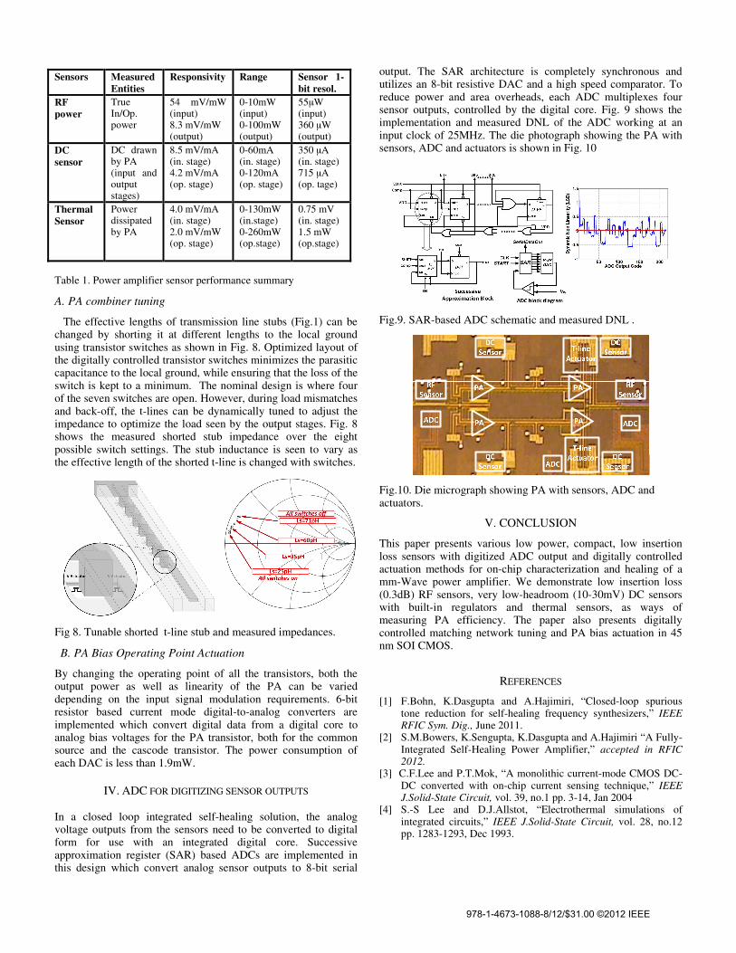
Table 1. Power amplifier sensor performance summary
A. PA combiner tuning
The effective lengths of transmission line stubs (Fig.1) can be changed by shorting it at different lengths to the local ground using transistor switches as shown in Fig. 8. Optimized layout of the digitally controlled transistor switches minimizes the parasitic capacitance to the local ground, while ensuring that the loss of the switch is kept to a minimum. The nominal design is where four of the seven switches are open. However, during load mismatches and back-off, the t-lines can be dynamically tuned to adjust the impedance to optimize the load seen by the output stages. Fig. 8 shows the measured shorted stub impedance over the eight possible switch settings. The stub inductance is seen to vary as the effective length of the shorted t-line is changed with switches.
Fig 8. Tunable shorted t-line stub and measured impedances.
B. PA Bias Operating Point Actuation
By changing the operating point of all the transistors, both the output power as well as linearity of the PA can be varied depending on the input signal modulation requirements. 6-bit resistor based current mode digital-to-analog converters are implemented which convert digital data from a digital core to analog bias voltages for the PA transistor, both for the common source and the cascode transistor. The power consumption of each DAC is less than 1.9mW.
IV. ADC FOR DIGITIZING SENSOR OUTPUTS
In a closed loop integrated self-healing solution, the analog voltage outputs from the sensors need to be converted to digital form for use with an integrated digital core. Successive approximation register (SAR) based ADCs are implemented in this design which convert analog sensor outputs to 8-bit serial
output. The SAR architecture is completely synchronous and utilizes an 8-bit resistive DAC and a high speed comparator. To reduce power and area overheads, each ADC multiplexes four sensor outputs, controlled by the digital core. Fig. 9 shows the implementation and measured DNL of the ADC working at an input clock of 25MHz. The die photograph showing the PA with sensors, ADC and actuators is shown in Fig. 10
Fig.9. SAR-based ADC schematic and measured DNL .
Fig.10. Die micrograph showing PA with sensors, ADC and actuators.
V. CONCLUSION
This paper presents various low power, compact, low insertion loss sensors with digitized ADC output and digitally controlled actuation methods for on-chip characterization and healing of a mm-Wave power amplifier. We demonstrate low insertion loss (0.3dB) RF sensors, very low-headroom (10-30mV) DC sensors with built-in regulators and thermal sensors, as ways of measuring PA efficiency. The paper also presents digitally controlled matching network tuning and PA bias actuation in 45 nm SOI CMOS.
REFERENCES
[1] F.Bohn, K.Dasgupta and A.Hajimiri, “Closed-loop spurious tone reduction for self-healing frequency synthesizers,” IEEE RFIC Sym. Dig., June 2011.
[2] S.M.Bowers, K.Sengupta, K.Dasgupta and A.Hajimiri “A Fully-Integrated Self-Healing Power Amplifier,” accepted in RFIC 2012.
[3] C.F.Lee and P.T.Mok, “A monolithic current-mode CMOS DC-DC converted with on-chip current sensing technique,” IEEE J.Solid-State Circuit, vol. 39, no.1 pp. 3-14, Jan 2004
[4] S.-S Lee and D.J.Allstot, “Electrothermal simulations of integrated circuits,” IEEE J.Solid-State Circuit, vol. 28, no.12 pp. 1283-1293, Dec 1993.
Sensors Measured Entities
Responsivity Range Sensor 1-bit resol.
RF power
True In/Op. power
54 mV/mW (input) 8.3 mV/mW (output)
0-10mW (input) 0-100mW (output)
55µW (input) 360 µW (output)
DC sensor
DC drawn by PA (input and output stages)
8.5 mV/mA (in. stage) 4.2 mV/mA (op. stage)
0-60mA (in. stage) 0-120mA (op. stage)
350 µA (in. stage) 715 µA (op. tage)
Thermal Sensor
Power dissipated by PA
4.0 mV/mA (in. stage) 2.0 mV/mW (op. stage)
0-130mW (in.stage) 0-260mW (op.stage)
0.75 mV (in. stage) 1.5 mW (op.stage)
978-1-4673-1088-8/12/$31.00 ©2012 IEEE