old.vgamuseum.infoold.vgamuseum.info/images/stories/doc/3dfx/voodoo45_spec.doc · Web viewHigh...
379
Napalm Graphics Engine Napalm HIGH PERFORMANCE GRAPHICS ENGINE Revision 1.13 October 6, 1999 Copyright 1996-1999 3dfx Interactive, Inc. Revision 1.13 3dfx Confidential 1 Printed 2/19/2022 For Internal Use Only
Transcript of old.vgamuseum.infoold.vgamuseum.info/images/stories/doc/3dfx/voodoo45_spec.doc · Web viewHigh...

Napalm Graphics Engine
Napalm
HIGH PERFORMANCEGRAPHICS ENGINE
Revision 1.13October 6, 1999
Copyright 1996-1999 3dfx Interactive, Inc. All Rights Reserved
3dfx Interactive, Inc.4435 Fortran DriveSan Jose, CA 95134
Phone: (408) 935-4400Fax: (408) 935-4424
Copyright 1996-1999 3dfx Interactive, Inc. Revision 1.133dfx Confidential 1 Printed 5/7/2023
For Internal Use Only
Napalm Graphics Engine
1. INTRODUCTION........................................................................................................................... 11
1.1 RESOLUTIONS........................................................................................................................... 12
2. PERFORMANCE..................................................................................................................... 13
2.1 2D PERFORMANCE.................................................................................................................... 132.2 3D PERFORMANCE.................................................................................................................... 13
3. FUNCTIONAL OVERVIEW....................................................................................................14
3.1 SYSTEM LEVEL DIAGRAMS.......................................................................................................143.2 ARCHITECTURAL OVERVIEW.....................................................................................................15
3.2.1 Overall Overview............................................................................................................. 153.2.2 Detailed Datapath Diagram.............................................................................................163.2.3 FBI/TMU......................................................................................................................... 163.2.4 2D................................................................................................................................... 18
3.3 FUNCTIONAL OVERVIEW........................................................................................................... 183.4 MODIFICATIONS FROM SST1.....................................................................................................223.5 ADDITIONS TO AVENGER FROM BANSHEE..................................................................................233.6 ADDITIONS TO NAPALM FROM AVENGER...................................................................................233.7 PROGRAMMING NOTES ON AVENGER VS. BANSHEE...................................................................24
4. NAPALM ADDRESS SPACE....................................................................................................25
5. VGA REGISTER SET.............................................................................................................. 27
5.1 OVERVIEW OF THE NAPALM VGA CONTROLLER........................................................................275.2 USING VGA REGISTERS WHEN NAPALM IS NOT THE PRIMARY VGA..........................................275.3 LOCKING VGA TIMING FOR VIRTUALIZED MODES....................................................................275.4 SETTING VGA TIMING FOR VIDEO 2 PIXELS PER CLOCK MODE.................................................275.5 GENERAL REGISTERS:...............................................................................................................31
5.5.1 Input Status 0 (0x3C2).....................................................................................................315.5.2 Input Status 1 (0x3BA/0x3DA).........................................................................................315.5.3 Feature Control Write (0x3BA/0x3DA)............................................................................315.5.4 Feature Control Read (0x3CA)........................................................................................315.5.5 Miscellaneous Output (0x3CC)........................................................................................325.5.6 Motherboard Enable (0x3C3)...........................................................................................325.5.7 Adapter Enable (0x46E8).................................................................................................325.5.8 Subsystem Enable (0x102)................................................................................................32
5.6 CRTC REGISTERS:................................................................................................................... 335.6.1 CRTC Index Register (0x3B4/0x3D4)...............................................................................345.6.2 Index 0x0-Horizontal Total (0x3B5/0x3D5)......................................................................345.6.3 Index 0x1-Horizontal Display Enable End (0x3B5/0x3D5)...............................................345.6.4 Index 0x2-Start Horizontal Blanking (0x3B5/0x3D5).......................................................355.6.5 Index 0x3-End Horizontal Blanking (0x3B5/0x3D5).........................................................355.6.6 Index 0x4-Start Horizontal Sync (0x3B5/0x3D5)..............................................................355.6.7 Index 0x5-End Horizontal Sync (0x3B5/0x3D5)...............................................................355.6.8 Index 0x6-Vertical Total (0x3B5/0x3D5)..........................................................................365.6.9 Index 0x7-Overflow (0x3B5/0x3D5).................................................................................365.6.10 Index 0x8-Preset Row Scan (0x3B5/0x3D5).....................................................................365.6.11 Index 0x9-Maximum Scan Line (0x3B5/0x3D5)................................................................375.6.12 Index 0xA-Cursor Start (0x3B5/0x3D5)............................................................................37
Copyright 1996-1999 3dfx Interactive, Inc. Revision 1.133dfx Confidential 2 Printed 5/7/2023
For Internal Use Only
Napalm Graphics Engine
5.6.13 Index 0xB-Cursor End (0x3B5/0x3D5).............................................................................375.6.14 Index 0xC-Start Address High (0x3B5/0x3D5)..................................................................375.6.15 Index 0xD-Start Address Low (0x3B5/0x3D5)..................................................................375.6.16 Index 0xE-Cursor Location High (0x3B5/0x3D5).............................................................375.6.17 Index 0xF-Cursor Location Low (0x3B5/0x3D5)..............................................................385.6.18 Index 0x10-Vertical Retrace Start (0x3B5/0x3D5)............................................................385.6.19 Index 0x11-Vertical Retrace End (0x3B5/0x3D5)..............................................................385.6.20 Index 0x12-Vertical Display Enable End (0x3B5/0x3D5).................................................385.6.21 Index 0x13-Offset (0x3B5/0x3D5)....................................................................................395.6.22 Index 0x14-Underline Location (0x3B5/0x3D5)...............................................................395.6.23 Index 0x15-Start Vertical Blank (0x3B5/0x3D5)...............................................................395.6.24 Index 0x16-End Vertical Blank (0x3B5/0x3D5)................................................................395.6.25 Index 0x17-CRTC Mode Control (0x3B5/0x3D5).............................................................405.6.26 Index 0x18-Line Compare (0x3B5/0x3D5)........................................................................405.6.27 Index 0x1A-Horizontal Extension Register (0x3B5/0x3D5)...............................................405.6.28 Index 0x1B-Vertical Extension Register (0x3B5/0x3D5)...................................................405.6.29 Index 0x1C-PCI Config/Extension Byte 0 (0x3B5/0x3D5)................................................415.6.30 Index 0x1D-Extension Byte 1 (0x3B5/0x3D5)...................................................................415.6.31 Index 0x1E-Extension Byte 2 (0x3B5/0x3D5)...................................................................425.6.32 Index 0x1F-Extension Byte 3 (0x3B5/0x3D5)...................................................................425.6.33 Index 0x20-Vertical Counter pre-load Low (0x3B5/0x3D5)..............................................425.6.34 Index 0x21- Vertical Counter pre-load High(0x3B5/0x3D5).............................................425.6.35 Index 0x22-Latch Read Back (0x3B5/0x3D5)...................................................................425.6.36 Index 0x24-Attribute Controller Index/Data State (0x3B5/0x3D5)....................................425.6.37 Index 0x26-Display Bypass/Attribute Controller Index (0x3B5/0x3D5)............................43
5.7 GRAPHICS CONTROLLER REGISTERS:.........................................................................................445.7.1 Graphics Controller Index Register (0x3CE)....................................................................445.7.2 Index 0-Set/Reset (0x3CF)...............................................................................................445.7.3 Index 1-Enable Set/Reset (0x3CF)...................................................................................445.7.4 Index 2-Color Compare (0x3CF)......................................................................................445.7.5 Index 3-Data Rotate (0x3CF)...........................................................................................455.7.6 Index 4-Read Map Select (0x3CF)...................................................................................455.7.7 Index 5-Graphics Mode (0x3CF)......................................................................................455.7.8 Index 6-Miscellaneous (0x3CF).......................................................................................465.7.9 Index 7-Color Don’t Care (0x3CF)...................................................................................465.7.10 Index 8-Mask (0x3CF).....................................................................................................46
5.8 ATTRIBUTE REGISTERS............................................................................................................. 475.8.1 Attribute Index Register (0x3C0)......................................................................................475.8.2 Index 0x0 through 0xF-Palette Registers (0x3C0/3C1).....................................................475.8.3 Index 10-Attribute Mode Control Register (0x3C0)..........................................................475.8.4 Index 11-Over Scan Control Register (0x3C0)..................................................................475.8.5 Index 12-Color Plane Enable Register (0x3C0)................................................................485.8.6 Index 13-Horizontal Pixel Panning Register (0x3C0).......................................................485.8.7 Index 14-Color Select Register (0x3C0)...........................................................................48
5.9 SEQUENCER REGISTERS............................................................................................................ 495.9.1 Sequencer Index Register (0x3c4)....................................................................................495.9.2 Index 0-Reset (0x3c5)......................................................................................................495.9.3 Index 1-Clocking Mode (0x3c5).......................................................................................495.9.4 Index 2-Map Mask (0x3c5)...............................................................................................495.9.5 Index 3-Character Map Select (0x3c5).............................................................................495.9.6 Index 4-Memory Mode (0x3c5)........................................................................................51
5.10 RAMDAC REGISTERS.............................................................................................................. 52
Copyright 1996-1999 3dfx Interactive, Inc. Revision 1.133dfx Confidential 3 Printed 5/7/2023
For Internal Use Only

Napalm Graphics Engine
5.10.1 RAMDAC Pixel Mask (0x3c6)..........................................................................................525.10.2 RAMDAC Read Index /Read Status (0x3c7).....................................................................52
5.11 RAMDAC WRITE INDEX (0X3C8)............................................................................................525.11.1 RAMDAC Data (0x3c9)...................................................................................................52
6. ACCESSING MEMORY IN VESA MODES...........................................................................53
7. 2D............................................................................................................................................... 53
7.1 2D REGISTER MAP................................................................................................................... 537.2 REGISTER DESCRIPTIONS..........................................................................................................55
7.2.1 status Register................................................................................................................. 557.2.2 command Register............................................................................................................ 557.2.3 commandExtra Register...................................................................................................577.2.4 colorBack and colorFore Registers..................................................................................577.2.5 Pattern Registers............................................................................................................. 587.2.6 srcBaseAddr and dstBaseAddr Registers..........................................................................587.2.7 srcSize and dstSize Registers............................................................................................597.2.8 srcXY and dstXY Registers...............................................................................................597.2.9 srcFormat and dstFormat Registers.................................................................................607.2.10 clip0Min, clip0Max, clip1Min, and clip1Max Registers...................................................627.2.11 colorkey Registers............................................................................................................637.2.12 rop Register..................................................................................................................... 647.2.13 lineStyle register.............................................................................................................. 647.2.14 lineStipple Register..........................................................................................................667.2.15 bresenhamError registers.................................................................................................67
7.3 LAUNCH AREA......................................................................................................................... 677.3.1 Screen-to-screen Blt Mode...............................................................................................677.3.2 Screen-to-screen Stretch Blt Mode...................................................................................687.3.3 Host-to-screen Blt Mode..................................................................................................687.3.4 Host-to-screen Stretch Blt Mode.......................................................................................707.3.5 Rectangle Fill Mode........................................................................................................ 707.3.6 Line Mode........................................................................................................................ 707.3.7 Polyline Mode.................................................................................................................. 717.3.8 Polygon Fill Mode...........................................................................................................72
7.4 MISCELLANEOUS 2D................................................................................................................ 807.4.1 Write Sgram/Sdram Mode Register..................................................................................807.4.2 Write Sgram Color Register.............................................................................................817.4.3 Write Sgram Mask Register..............................................................................................81
8. 3D MEMORY MAPPED REGISTER SET..............................................................................81
8.1 STATUS REGISTER..................................................................................................................... 878.2 INTRCTRL REGISTER.................................................................................................................878.3 VERTEX AND FVERTEX REGISTERS.............................................................................................888.4 STARTR, STARTG, STARTB, STARTA, FSTARTR, FSTARTG, FSTARTB, AND FSTARTA REGISTERS.....898.5 STARTZ AND FSTARTZ REGISTERS..............................................................................................898.6 STARTS, STARTT, FSTARTS, AND FSTARTT REGISTERS.................................................................908.7 STARTW AND FSTARTW REGISTERS...........................................................................................908.8 DRDX, DGDX, DBDX, DADX, FDRDX, FDGDX, FDBDX, AND FDADX REGISTERS.....................908.9 DZDX AND FDZDX REGISTERS.................................................................................................918.10 DSDX, DTDX, FDSDX, AND FDTDX REGISTERS........................................................................918.11 DWDX AND FDWDX REGISTERS...............................................................................................928.12 DRDY, DGDY, DBDY, DADY, FDRDY, FDGDY, FDBDY, AND FDADY REGISTERS........................92Copyright 1996-1999 3dfx Interactive, Inc. Revision 1.133dfx Confidential 4 Printed 5/7/2023
For Internal Use Only
Napalm Graphics Engine 8.13 DZDY AND FDZDY REGISTERS.................................................................................................928.14 DSDY, DTDY, FDSDY, AND FDTDY REGISTERS..........................................................................938.15 DWDY AND FDWDY REGISTERS...............................................................................................938.16 TRIANGLECMD AND FTRIANGLECMD REGISTERS.....................................................................938.17 NOPCMD REGISTER................................................................................................................. 948.18 FASTFILLCMD REGISTER..........................................................................................................948.19 SWAPBUFFERCMD REGISTER....................................................................................................958.20 FBZCOLORPATH REGISTER........................................................................................................ 968.21 COMBINEMODE REGISTER.......................................................................................................1018.22 FOGMODE REGISTER.............................................................................................................. 1028.23 ALPHAMODE REGISTER...........................................................................................................104
8.23.1 Alpha function...............................................................................................................1058.23.2 Alpha Blending.............................................................................................................. 106
8.24 LFBMODE REGISTER...............................................................................................................1088.24.1 Linear Frame Buffer Writes............................................................................................110
8.25 FBZMODE REGISTER............................................................................................................... 1158.25.1 Depth-buffering function................................................................................................119
8.26 RENDERMODE REGISTER.........................................................................................................1208.27 STENCILMODE REGISTER........................................................................................................1228.28 STENCILOP REGISTER.............................................................................................................1238.29 SLICTRL REGISTER................................................................................................................. 1248.30 AACTRL REGISTER.................................................................................................................1248.31 CHIPMASK REGISTER.............................................................................................................. 1258.32 STIPPLE REGISTER................................................................................................................... 1268.33 COLOR0 REGISTER.................................................................................................................. 1268.34 COLOR1 REGISTER.................................................................................................................. 1268.35 FOGCOLOR REGISTER............................................................................................................. 1268.36 ZACOLOR REGISTER............................................................................................................... 1278.37 CHROMAKEY REGISTER.......................................................................................................... 1278.38 CHROMARANGE REGISTER......................................................................................................1278.39 USERINTRCMD REGISTER.......................................................................................................1288.40 COLBUFFERADDR................................................................................................................... 1298.41 COLBUFFERSTRIDE.................................................................................................................1298.42 AUXBUFFERADDR.................................................................................................................. 1298.43 AUXBUFFERSTRIDE................................................................................................................. 1308.44 CLIPLEFTRIGHT AND CLIPTOPBOTTOM REGISTERS..................................................................1308.45 CLIPLEFTRIGHT1, CLIPTOPBOTTOM1 REGISTERS.....................................................................1318.46 FOGTABLE REGISTER.............................................................................................................. 1328.47 FBIPIXELSIN REGISTER........................................................................................................... 1328.48 FBICHROMAFAIL REGISTER.....................................................................................................1328.49 FBIZFUNCFAIL REGISTER........................................................................................................1328.50 FBIAFUNCFAIL REGISTER........................................................................................................ 1338.51 FBISTENCILTESTFAIL REGISTER...............................................................................................1338.52 FBIPIXELSOUT REGISTER........................................................................................................1338.53 SWAPBUFFERPEND REGISTER..................................................................................................1338.54 LEFTOVERLAYBUF REGISTER..................................................................................................1338.55 RIGHTOVERLAYBUF REGISTER...............................................................................................1348.56 LEFTDESKTOPBUF REGISTER...................................................................................................1348.57 FBISWAPHISTORY REGISTER....................................................................................................1348.58 FBITRIANGLESOUT REGISTER..................................................................................................1348.59 SSETUPMODE REGISTER.........................................................................................................1358.60 TRIANGLE SETUP VERTEX REGISTERS.....................................................................................135
Copyright 1996-1999 3dfx Interactive, Inc. Revision 1.133dfx Confidential 5 Printed 5/7/2023
For Internal Use Only

Napalm Graphics Engine 8.61 SARGB REGISTER.................................................................................................................. 1368.62 SRED REGISTER...................................................................................................................... 1368.63 SGREEN REGISTER.................................................................................................................. 1368.64 SBLUE REGISTER.................................................................................................................... 1368.65 SALPHA REGISTER.................................................................................................................. 1368.66 SVZ REGISTER........................................................................................................................ 1378.67 SWB REGISTER....................................................................................................................... 1378.68 SWTMU0 REGISTER................................................................................................................ 1378.69 SS/W0 REGISTER.................................................................................................................... 1378.70 ST/W0 REGISTER................................................................................................................... 1378.71 SWTMU1 REGISTER................................................................................................................ 1378.72 SS/WTMU1 REGISTER............................................................................................................. 1378.73 ST/WTMU1 REGISTER............................................................................................................. 1388.74 SDRAWTRICMD REGISTER.....................................................................................................1388.75 SBEGINTRICMD REGISTER.....................................................................................................1388.76 TEXTUREMODE REGISTER.......................................................................................................1408.77 TLOD REGISTER.................................................................................................................... 1468.78 TDETAIL REGISTER.................................................................................................................1488.79 TEXBASEADDR, TEXBASEADDR1, TEXBASEADDR2, AND TEXBASEADDR38 REGISTERS...........1488.80 TREXINIT1 REGISTER.............................................................................................................. 1498.81 NCCTABLE0 AND NCCTABLE1 REGISTERS...............................................................................1498.82 8-BIT PALETTE....................................................................................................................... 1508.83 COMMAND DESCRIPTIONS.......................................................................................................151
8.83.1 NOP Command..............................................................................................................1518.83.2 TRIANGLE Command....................................................................................................1518.83.3 FASTFILL Command......................................................................................................1528.83.4 SWAPBUFFER Command..............................................................................................1528.83.5 USERINTERRUPT Command........................................................................................153
8.84 LINEAR FRAME BUFFER ACCESS (* FIX THIS *)....................................................................1538.84.1 Linear frame buffer Writes.............................................................................................1548.84.2 Linear frame buffer Reads..............................................................................................155
9. 1. PLL REGISTERS................................................................................................................ 155
1.1 PLLCTRL0, PLLCTRL1 REGISTERS...........................................................................................1551.2 TK532_PLL MODIFICATIONS FOR NAPALM............................................................................1569.1 TEST MODE............................................................................................................................ 156
10. 2. DAC REGISTERS............................................................................................................... 157
10.1 2.1 DACMODE........................................................................................................................ 15710.2 2.2 DACADDR......................................................................................................................... 15710.3 2.3 DACDATA......................................................................................................................... 157
11. 3. VIDEO REGISTERS(PCI)..................................................................................................158
11.1.1 3.1.1 vidTvOutBlankVCount...........................................................................................15811.1.2 3.1.2 vidMaxRgbDelta...................................................................................................15911.1.3 3.1.3 vidProcCfg Register..............................................................................................15911.1.4 3.1.4 hwCurPatAddr Register........................................................................................16111.1.5 3.1.5 hwCurLoc Register................................................................................................16211.1.6 3.1.6 hwCurC0 Register.................................................................................................16211.1.7 3.1.7 hwCurC1 Register.................................................................................................16211.1.8 3.1.8 vidInFormat..........................................................................................................16211.1.9 3.1.9 vidSerialParallelPort Register..............................................................................164
Copyright 1996-1999 3dfx Interactive, Inc. Revision 1.133dfx Confidential 6 Printed 5/7/2023
For Internal Use Only

Napalm Graphics Engine
11.1.10 3.1.10 vidTvOutBlankHCount.....................................................................................16711.1.11 3.1.11 vidInXDecimDeltas (for VMI downscaling Brensenham Engine)/ vidTvOutBlankHCount (for TV out master mode)..............................................................................16811.1.12 3.1.12 vidInDecimInitErrs..........................................................................................16811.1.13 3.1.13 vidInYDecimDeltas..........................................................................................16811.1.14 3.1.14 vidPixelBufThold.............................................................................................16911.1.15 3.1.15 vidChromaKeyMin Register.............................................................................16911.1.16 3.1.16 vidChromaKeyMax Register............................................................................17011.1.17 3.1.17 vidInStatusCurrentLine Register......................................................................17011.1.18 3.1.18 vidScreenSize...................................................................................................17011.1.19 3.1.19 vidOverlayStartCoords....................................................................................17011.1.20 3.1.20 vidOverlayEndScreenCoord.............................................................................17111.1.21 3.1.21 vidOverlayDudx...............................................................................................17111.1.22 3.1.22 vidOverlayDudxOffsetSrcWidth.......................................................................17111.1.23 3.1.23 vidOverlayDvdy...............................................................................................17111.1.24 3.1.24 vidOverlayDvdyOffset......................................................................................17111.1.25 3.1.25 vidDesktopStartAddr........................................................................................17211.1.26 3.1.26 vidDesktopOverlayStride.................................................................................17211.1.27 3.1.27 vidInAddr0......................................................................................................17311.1.28 3.1.28 vidInAddr1......................................................................................................17311.1.29 3.1.29 vidInAddr2......................................................................................................17311.1.30 3.1.30 vidInStride.......................................................................................................17311.1.31 3.1.31 vidCurrOverlayStartAddr................................................................................173
11.2 3.2 VIDEO-IN INTERFACE.......................................................................................................17411.2.1 3.2.1 Function................................................................................................................17411.2.2 3.2.2 Signals.................................................................................................................. 174
11.3 3.3 VIDEO LIMITATION............................................................................................................175
12. COMMAND TRANSPORT PROTOCOL..............................................................................176
12.1 COMMAND TRANSPORT........................................................................................................... 17612.1.1 CMDFIFO Management................................................................................................17612.1.2 CMDFIFO Data............................................................................................................17712.1.3 CMDFIFO Packet Type 0...............................................................................................17712.1.4 CMDFIFO Packet Type 1...............................................................................................17812.1.5 CMDFIFO Packet Type 2...............................................................................................17812.1.6 CMDFIFO Packet Type 3...............................................................................................17912.1.7 CMDFIFO Packet Type 4...............................................................................................18012.1.8 CMDFIFO Packet Type 5...............................................................................................18112.1.9 CMDFIFO Packet Type 6...............................................................................................18212.1.10 Miscellaneous............................................................................................................182
13. AGP/CMD TRANSFER/MISC REGISTERS........................................................................182
13.1 AGPREQSIZE........................................................................................................................... 18313.2 AGPHOSTADDRESSLOW..........................................................................................................18313.3 AGPHOSTADDRESSHIGH.........................................................................................................18413.4 AGPGRAPHICSADDRESS..........................................................................................................18413.5 AGPGRAPHICSSTRIDE.............................................................................................................. 18413.6 AGPMOVECMD...................................................................................................................... 184
14. COMMAND FIFO REGISTERS............................................................................................185
14.1 CMDBASEADDR0.................................................................................................................... 18514.2 CMDBASESIZE0...................................................................................................................... 186Copyright 1996-1999 3dfx Interactive, Inc. Revision 1.133dfx Confidential 7 Printed 5/7/2023
For Internal Use Only
Napalm Graphics Engine 14.3 CMDBUMP0............................................................................................................................ 18614.4 CMDRDPTRL0........................................................................................................................ 18614.5 CMDRDPTRH0........................................................................................................................ 18614.6 CMDAMIN0............................................................................................................................ 18614.7 CMDAMAX0........................................................................................................................... 18614.8 CMDSTATUS0.......................................................................................................................... 18714.9 CMDFIFODEPTH0.................................................................................................................... 18714.10 CMDHOLECNT0.................................................................................................................. 18714.11 CMDBASEADDR1................................................................................................................18714.12 CMDBASESIZE1.................................................................................................................. 18814.13 CMDBUMP1........................................................................................................................ 18814.14 CMDRDPTRL1.................................................................................................................... 18814.15 CMDRDPTRH1.................................................................................................................... 18814.16 CMDAMIN1........................................................................................................................ 18814.17 CMDAMAX1....................................................................................................................... 18814.18 CMDSTATUS1...................................................................................................................... 18814.19 CMDFIFODEPTH1................................................................................................................18814.20 CMDHOLECNT1.................................................................................................................. 18914.21 CMDFIFOTHRESH................................................................................................................18914.22 CMDHOLEINT..................................................................................................................... 18914.23 YUVBASEADDRESS.............................................................................................................18914.24 YUVSTRIDE......................................................................................................................... 189
15. AGP/PCI CONFIGURATION REGISTER SET...................................................................190
15.1 VENDOR_ID REGISTER........................................................................................................... 19115.2 DEVICE_ID REGISTER.............................................................................................................19115.3 COMMAND REGISTER.............................................................................................................. 19115.4 STATUS REGISTER................................................................................................................... 19115.5 REVISION_ID REGISTER..........................................................................................................19215.6 CLASS_CODE REGISTER.......................................................................................................... 19215.7 CACHE_LINE_SIZE REGISTER..................................................................................................19215.8 LATENCY_TIMER REGISTER.....................................................................................................19215.9 HEADER_TYPE REGISTER........................................................................................................ 19215.10 BIST REGISTER.................................................................................................................. 19315.11 MEMBASEADDR0 REGISTER................................................................................................19315.12 MEMBASEADDR1 REGISTER................................................................................................19415.13 IOBASEADDR REGISTER......................................................................................................19515.14 SUBVENDORID REGISTER...................................................................................................19615.15 SUBSYSTEMID REGISTER....................................................................................................19615.16 ROMBASEADDR REGISTER..................................................................................................19615.17 CAPABILITIES POINTER........................................................................................................19615.18 INTERRUPT_LINE REGISTER.................................................................................................19615.19 INTERRUPT_PIN REGISTER...................................................................................................19715.20 MIN_GNT REGISTER............................................................................................................ 19715.21 MAX_LAT REGISTER........................................................................................................... 19715.22 FABID REGISTER................................................................................................................. 19715.23 ACPI RESET REGISTER.......................................................................................................19715.24 CFGINITENABLE REGISTER..................................................................................................19715.25 CFGPCIDECODE REGISTER...................................................................................................19815.26 CFGVIDEOCTRL0, CFGVIDEOCTRL1, AND CFGVIDEOCTRL2 REGISTERS................................19915.27 CFGSLILFBCTRL REGISTER.................................................................................................20215.28 CFGAADEPTHBUFFERAPERTURE REGISTER..........................................................................202Copyright 1996-1999 3dfx Interactive, Inc. Revision 1.133dfx Confidential 8 Printed 5/7/2023
For Internal Use Only

Napalm Graphics Engine 15.29 CFGAALFBCTRL REGISTER.................................................................................................20315.30 CFGSLIAAMISC REGISTER...................................................................................................20315.31 CFGSTATUS REGISTER......................................................................................................... 20415.32 CFGSCRATCH REGISTER.......................................................................................................20515.33 NEW CAPABILITIES (AGP AND ACPI)..................................................................................20515.34 CAPABILITY IDENTIFIER REGISTER.......................................................................................20515.35 AGP STATUS...................................................................................................................... 20515.36 AGP COMMAND................................................................................................................. 20515.37 ACPI CAP ID..................................................................................................................... 20715.38 ACPI CTRL/STATUS............................................................................................................207
16. INIT REGISTERS................................................................................................................... 208
16.1 STATUS REGISTER (0X0)..........................................................................................................20816.2 PCIINIT0 REGISTER (0X4)........................................................................................................ 20916.3 SIPMONITOR REGISTER (0X8)..................................................................................................21016.4 LFBMEMORYCONFIG REGISTER (0XC).....................................................................................21016.5 MISCINIT0 REGISTER (0X10)...................................................................................................21216.6 MISCINIT1 REGISTER (0X14 WHEN MISCINIT0[30]=0).............................................................21316.7 VIP2VMICTRL REGISTER (0X14 WHEN MISCINIT0[30]=1).........................................................21516.8 DRAMINIT0 REGISTER (0X18).................................................................................................21516.9 DRAMINIT1 REGISTER (0X1C).................................................................................................21716.10 AGPINIT0 REGISTER (0X20).................................................................................................21816.11 TMUGBEINIT REGISTER (0X24)...........................................................................................21816.12 VGAINIT0 REGISTER (0X28)...............................................................................................21816.13 VGAINIT1 REGISTER (0X2C)...............................................................................................22016.14 2D_COMMAND_REGISTER (0X30)......................................................................................22116.15 2D_SRCBASEADDR REGISTER (0X34).................................................................................22116.16 STRAPINFO REGISTER (0X38)..............................................................................................22116.17 IMATCHCTRL REGISTER (0X48)..........................................................................................221
17. FRAME BUFFER ACCESS....................................................................................................222
17.1 FRAME BUFFER ORGANIZATION..............................................................................................22217.2 LINEAR FRAME BUFFER ACCESS.............................................................................................22217.3 TILED FRAME BUFFER ACCESS................................................................................................223
18. YUV PLANAR ACCESS......................................................................................................... 224
19. TEXTURE MEMORY ACCESS.............................................................................................226
19.1 WRITING TO TEXTURE SPACE..................................................................................................22619.2 CALCULATING TEXEL ADDRESSES............................................................................................23119.3 MAINTAINING CACHE COHERENCY IN NAPALM........................................................................232
20. PROGRAMMING TIPS & CAVEATS...................................................................................233
20.1 MEMORY ACCESSES................................................................................................................ 23320.2 DETERMINING NAPALM IDLE CONDITION................................................................................23320.3 TRIANGLE SUBPIXEL CORRECTION..........................................................................................23420.4 32 BPP RENDERING...............................................................................................................23420.5 15 BPP RENDERING...............................................................................................................23420.6 2 PIXEL-PER-CLOCK RENDERING.............................................................................................23520.7 SCANLINE INTERLEAVING........................................................................................................23520.8 MISCELLANEOUS CONTROL.....................................................................................................236
Copyright 1996-1999 3dfx Interactive, Inc. Revision 1.133dfx Confidential 9 Printed 5/7/2023
For Internal Use Only

Napalm Graphics Engine 21. ACCESSING THE ROM........................................................................................................236
21.1 ROM CONFIGURATION........................................................................................................... 23621.2 ROM READS.......................................................................................................................... 23621.3 ROM WRITES........................................................................................................................ 237
22. POWER ON STRAPPING PINS............................................................................................237
23. SIGNAL STRAPPING............................................................................................................239
24. MONITOR SENSE.................................................................................................................. 239
25. DATA FORMATS.................................................................................................................... 239
26. ISSUES/REQUIREMENTS....................................................................................................240
26.1 PCI/AGP REQUIREMENTS.......................................................................................................24026.2 2D REQUIREMENTS (SST-G)...................................................................................................24026.3 VIDEO / MONITOR REQUIREMENTS..........................................................................................24026.4 VGA CONTROLLER REQUIREMENTS........................................................................................24126.5 MEMORY CONTROLLER REQUIREMENTS..................................................................................24126.6 CONFIGURATION EEPROM.......................................................................................................24126.7 DAC REQUIREMENTS...............................................................................................................24226.8 PLL REQUIREMENTS............................................................................................................... 24226.9 OVERALL REQUIREMENTS.......................................................................................................24226.10 PC97 REQUIREMENTS.......................................................................................................... 24226.11 TESTABILITY REQUIREMENTS...............................................................................................242
27. REVISION HISTORY............................................................................................................. 243
Copyright 1996-1999 3dfx Interactive, Inc. Revision 1.133dfx Confidential 10 Printed 5/7/2023
For Internal Use Only
Napalm Graphics Engine
1. Introduction The Napalm Graphics Engine is a fifth (Voodoo Graphics, Voodoo2, Voodoo Banshee, Voodoo3, …) generation 3D graphics engine based on the original SST1 architecture. Napalm incorporates all of the original SST1 features such as true-perspective texture mapping with advanced mipmapping and lighting, texture anti-aliasing, sub-pixel correction, gouraud shading, depth-buffering, alpha blending and dithering. Napalm also has 2 full-featured texturing units, which allow for advanced features like trilinear filtering, dual-texturing or bump mapping to be performed at the rate of a pixel per clock. Also, Napalm incorporates true-color rendering, 24-bit depth, and stenciling capabilities. In addition to the SST1 features, Napalm includes a VGA core, 2D graphics acceleration, and support for Intel’s AGP 4x bus.
Features SST1 baseline features with 2 texturing units. SST1 software compatible AGP 4X / AGP2X / AGP 1X / PCI bus compliant Native 128-bit VGA core 2D acceleration
Binary/Ternary operand raster opsScreen to Screen, Screen to Texture space, and Texture space to Screen Blits.Color space conversion YUV to RGB.1:N monochrome expansionRendering support of 2048x2048
Integrated RAMDAC and PLLs. Bilinear video scaling Video in via feature connector Supports SGRAM and SDRAM memories TV out interface runs at 100MHz DDR
Video-In: Operates simultaneously with TV out interface. Decimation Support for interlaced video data Support VMI, SAA7110 video connectors Triple buffers for video-in data
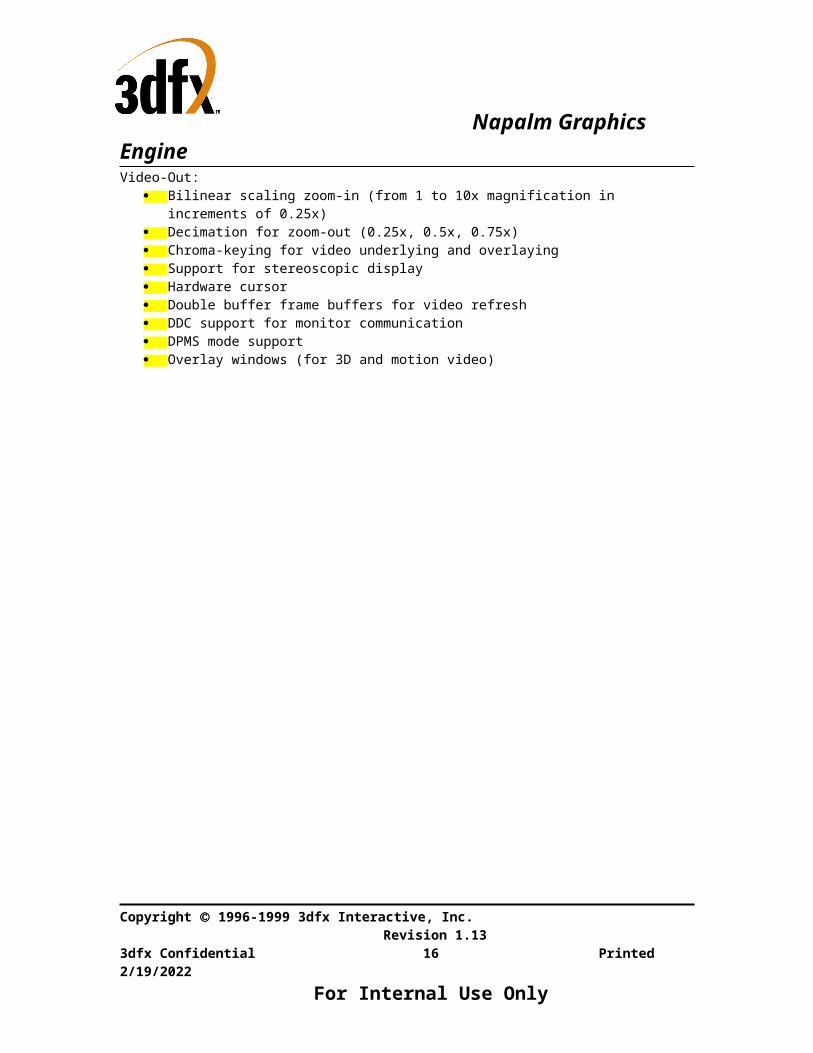
Video-Out: Bilinear scaling zoom-in (from 1 to 10x magnification in increments of 0.25x) Decimation for zoom-out (0.25x, 0.5x, 0.75x) Chroma-keying for video underlying and overlaying Support for stereoscopic display Hardware cursor Double buffer frame buffers for video refresh DDC support for monitor communication DPMS mode support Overlay windows (for 3D and motion video)
Copyright 1996-1999 3dfx Interactive, Inc. Revision 1.133dfx Confidential 11 Printed 5/7/2023
For Internal Use Only

Napalm Graphics Engine
1.1 Resolutions
VGAMODE # Mode Type # of Colors Native Resolution Alpha Format0,1 Alpha 16/256K 320x200 40x250,1 Alpha 16/256K 320x350 40x250,1 Alpha 16/256K 360x400 40x252,3 Alpha 16/256K 640x200 80x252,3 Alpha 16/256K 720x400 80x252,3 Alpha 16/256K 320x200 80x254,5 Graphics 4/256K 640x200 40x256 Graphics 2/256K 120x350 80x257 Alpha mono 320x200 80x25D Graphics 16/256K 640x350 40x25E Graphics 16/256K 640x350 40x25F Graphics mono 640x350 80x2510 Graphics 16/256K 640x350 80x2511 Graphics 2/256K 640x480 80x3012 Graphics 16/256K 640x480 80x3013 Graphics 256/256K 320x200 40x25
VESAMODE # Mode Type # of Colors Native Resolution Alpha Format100 Graphics 256/256K 640x400 80x25101 Graphics 256/256K 640x480 80x30
Copyright 1996-1999 3dfx Interactive, Inc. Revision 1.133dfx Confidential 12 Printed 5/7/2023
For Internal Use Only
Napalm Graphics Engine
2. Performance
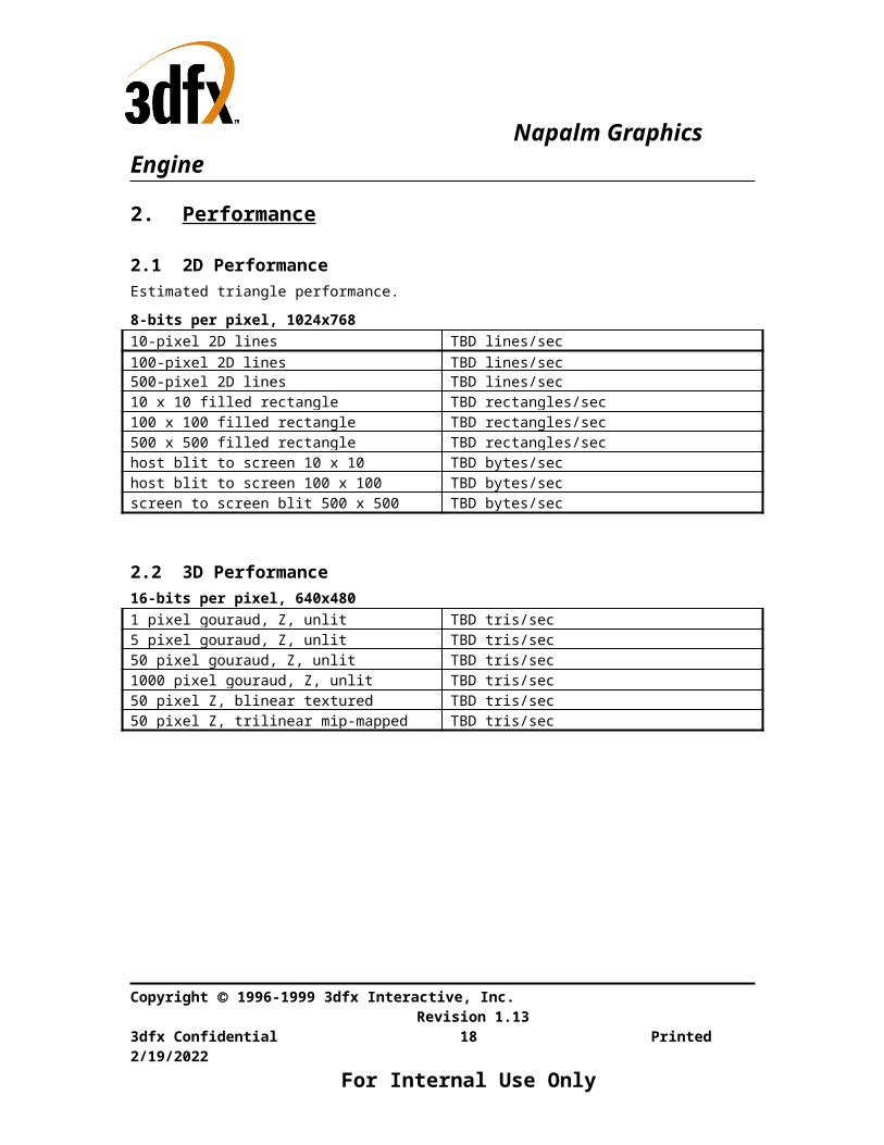
2.1 2D PerformanceEstimated triangle performance.
8-bits per pixel, 1024x768 resolution (linear)10-pixel 2D lines TBD lines/sec100-pixel 2D lines TBD lines/sec500-pixel 2D lines TBD lines/sec10 x 10 filled rectangle TBD rectangles/sec100 x 100 filled rectangle TBD rectangles/sec500 x 500 filled rectangle TBD rectangles/sechost blit to screen 10 x 10 TBD bytes/sechost blit to screen 100 x 100 TBD bytes/secscreen to screen blit 500 x 500 TBD bytes/sec
2.2 3D Performance16-bits per pixel, 640x4801 pixel gouraud, Z, unlit TBD tris/sec5 pixel gouraud, Z, unlit TBD tris/sec50 pixel gouraud, Z, unlit TBD tris/sec1000 pixel gouraud, Z, unlit TBD tris/sec50 pixel Z, blinear textured TBD tris/sec50 pixel Z, trilinear mip-mapped TBD tris/sec
Copyright 1996-1999 3dfx Interactive, Inc. Revision 1.133dfx Confidential 13 Printed 5/7/2023
For Internal Use Only

Napalm Graphics Engine
3. Functional Overview
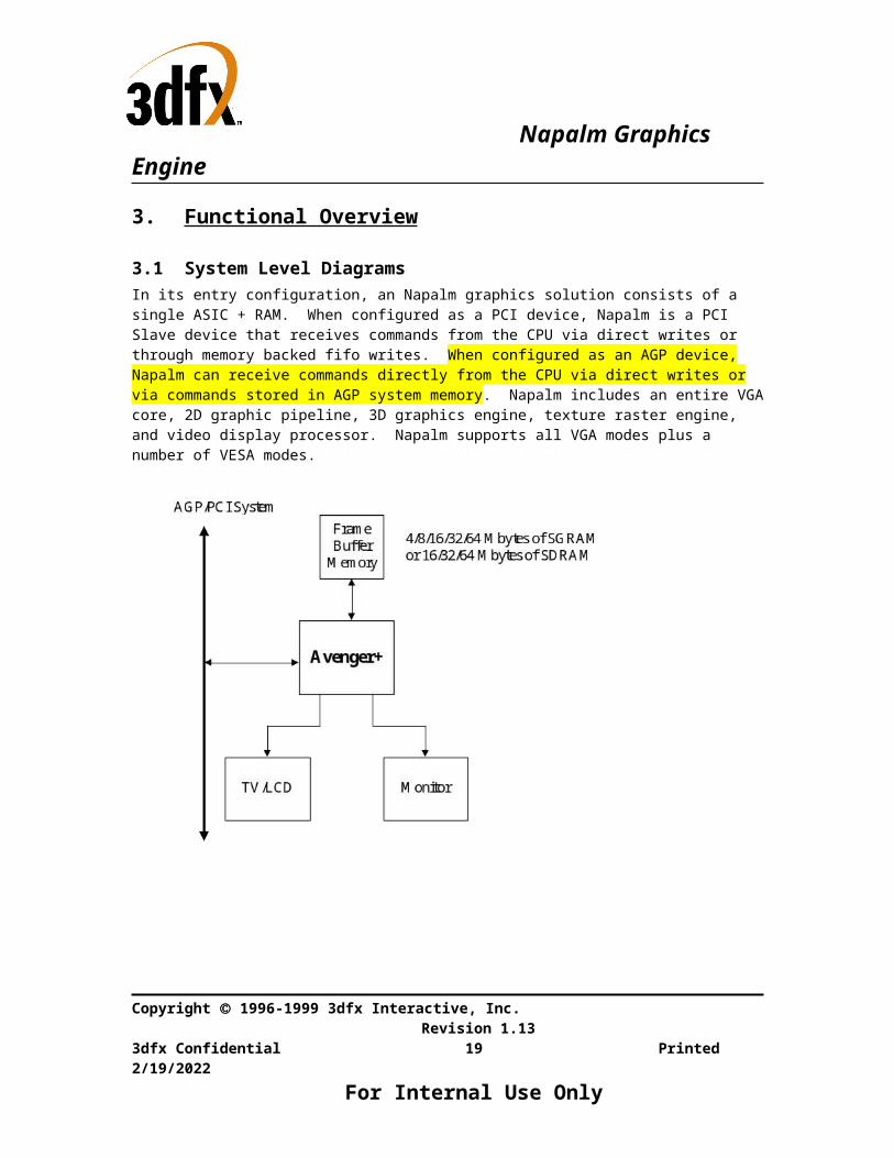
3.1 System Level DiagramsIn its entry configuration, an Napalm graphics solution consists of a single ASIC + RAM. When configured as a PCI device, Napalm is a PCI Slave device that receives commands from the CPU via direct writes or through memory backed fifo writes. When configured as an AGP device, Napalm can receive commands directly from the CPU via direct writes or via commands stored in AGP system memory. Napalm includes an entire VGA core, 2D graphic pipeline, 3D graphics engine, texture raster engine, and video display processor. Napalm supports all VGA modes plus a number of VESA modes.
Copyright 1996-1999 3dfx Interactive, Inc. Revision 1.133dfx Confidential 14 Printed 5/7/2023
For Internal Use Only

Napalm Graphics Engine
3.2 Architectural Overview
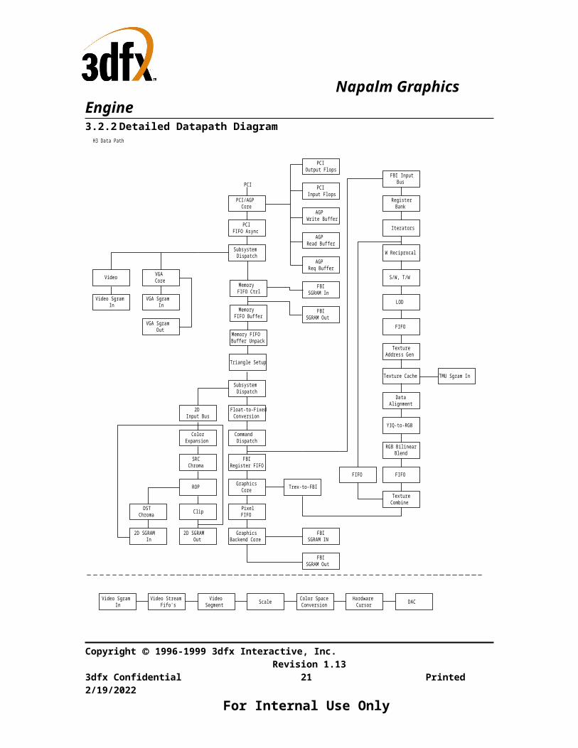
3.2.1 Overall OverviewThe diagram below illustrates the overall architecture of the Napalm graphics subsystem.
PCI/AGP Interface
CMD Fifos
FBI TMU2DVGAVIDEOIN
Memory Controller VIDEO
SGRAM PLL
PLLFeatureConnector
Copyright 1996-1999 3dfx Interactive, Inc. Revision 1.133dfx Confidential 15 Printed 5/7/2023
For Internal Use Only
Napalm Graphics Engine 3.2.2 Detailed Datapath Diagram
PCI
PCI/AGPCore
PCIOutput Flops
PCIInput Flops
AGPWrite Buffer
AGPRead Buffer
AGPReq Buffer
PCIFIFO Async
SubsystemDispatch
MemoryFIFO Ctrl
FBISGRAM In
FBISGRAM Out
MemoryFIFO Buffer
Memory FIFOBuffer Unpack
SubsystemDispatch
Float-to-FixedConversion
CommandDispatch
FBIRegister FIFO
GraphicsCore
PixelFIFO
GraphicsBackend Core
FBISGRAM IN
FBISGRAM Out
FBI InputBus
RegisterBank
Iterators
W Reciprocal
S/W, T/W
LOD
FIFO
TextureAddress Gen
Texture Cache TMU Sgram In
DataAlignment
YIQ-to-RGB
RGB BilinearBlend
FIFOFIFO
TextureCombine
2DInput Bus
ColorExpansion
SRCChroma
ROP
ClipDSTChroma
2D SGRAMIn
2D SGRAMOut
VGACore
VGA SgramIn
VGA SgramOut
H3 Data Path
Video
Video SgramIn
Trex-to-FBI
Video SgramIn
Video StreamFifo's
VideoSegment Scale Color Space
ConversionHardware
Cursor DAC
Triangle Setup
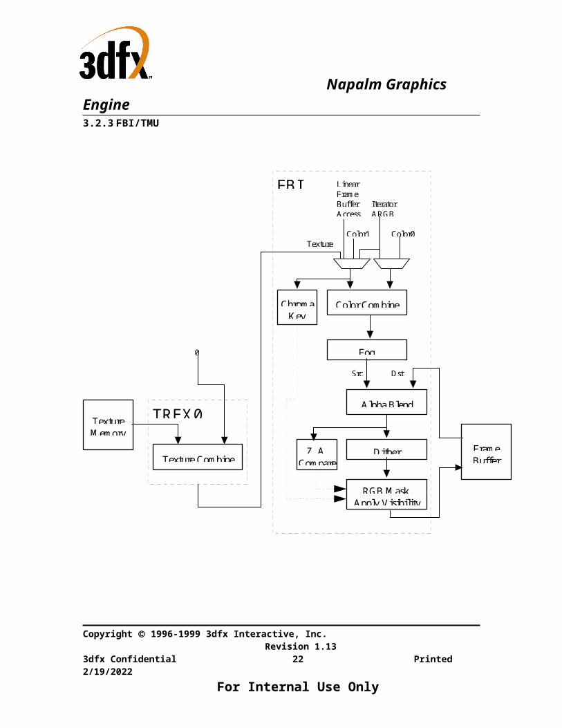
3.2.3 FBI/TMU
Copyright 1996-1999 3dfx Interactive, Inc. Revision 1.133dfx Confidential 16 Printed 5/7/2023
For Internal Use Only

Napalm Graphics Engine
Color Combine
IteratorARGB
Color0
Fog
Alpha Blend
FrameBuffer
Src Dst
RGB Mask,Apply Visibility
Z, ACompare
Dither
FBI
Texture
TREX0
Texture Combine
TextureMemory
0
Color1
LinearFrameBufferAccess
ChromaKey
Copyright 1996-1999 3dfx Interactive, Inc. Revision 1.133dfx Confidential 17 Printed 5/7/2023
For Internal Use Only
Napalm Graphics Engine 3.2.4 2D
Endian
4:N
1:N
8:N
SRCFIFO
256CLUT
ReplicateBytes
SRCChroma ROP
8x8x24Palette
DSTChroma
DSTFIFO
SRCADR
ADRFIFO
DSTADR
To Memory Ctrl
WriteBuffer
Endian
Endian
C0C1
1A
1A
LFB LFB’
LFB’LFB
Host Port
CLIP
C1C0
3.3 Functional OverviewNote: This section is horribly out-of-date and inaccurate. It was what was left over from the original Avenger spec…Please ignore this section…
Bus Support: Napalm implements both the PCI bus specification 2.1 and AGP specification 1.0 protocols, including support for the AGP 4x specification. Napalm is a slave only device on PCI, and a master device on AGP. Napalm supports zero-wait-state transactions and burst transfers.
PCI Bus Write Posting: Napalm uses an synchronous FIFO 32 entries deep which allows sufficient write posting capabilities for high performance. The FIFO is asynchronous to the graphics engine, thus allowing the memory interface to operate at maximum frequency regardless of the frequency of the PCI bus. Zero-wait-state writes are supported for maximum bus bandwidth.
VGA: Napalm includes a 100% IBM PS/2 model 70 compatible 128-bit VGA core, which is highly optimized for 128 bit memory transfers. The VGA core supports PC ’97 requirements for multiple adapter, and vga disable.
Copyright 1996-1999 3dfx Interactive, Inc. Revision 1.133dfx Confidential 18 Printed 5/7/2023
For Internal Use Only
Napalm Graphics Engine Memory FIFO: Napalm can optionally use off-screen frame buffer memory or AGP memory to increase the effective depth of the PCI bus FIFO. The depth of this memory FIFO is programmable, and when used as an addition to the regular 32 entry host FIFO, allows up to 1Mbyte host writes to be queued without stalling the PCI interface. Napalm supports 2 independent command streams that are asynchronous to each other. Either command stream can be located in AGP memory or frame buffer memory.
Memory Architecture: The frame buffer controller of Napalm has a 128-bit wide datapath to RGB, alpha/depth-buffer, 2D desktop, video, and texture memory with support for up to 200 MHz SGRAMs or SDRAMS. For 2D fills using the standard 2D bitBLT engine, 8 16-bit pixels are written per clock, resulting in a 800 Mpixel/sec peak fill rate. For screen clears using the color expansion capabilities specific to SGRAM, 64 bytes are written per clock, resulting in a 12.8 Gbytes/sec peak fill rate. For Gouraud-shaded or textured-mapped polygons with depth buffering enabled, one pixel is written per clock – this results in a 166 Mpixels/sec peak fill rate. The minimum amount of memory supported by Napalm is 4 Mbytes, with a maximum of 64 Mbytes supported.
Storing texture bitmaps, the texture memory controller of Napalm must share the 128-bit wide Datapath to Napalm memory. The texture unit uses sophisticated caching to reduce the required bandwidth of memory to perform bilinear texture filtering with no performance penalty. The amount of texture memory is only limited by the maximum amount of Napalm frame buffer memory.
Host Bus Addressing Schemes: Napalm occupies a combined 256 Mbytes of memory mapped address space, using two PCI memory base address pointers. Napalm also occupies 256 bytes of I/O mapped address space for video and initialization registers. The register space of Napalm occupies 6 Mbytes of address space, the linear frame buffer occupies 128 Mbytes of address space, the ordered texture download port occupies 2 Mbytes of address space, and the 3D pipeline linear frame buffer takes 8 Mbytes of address space.
2D Architecture: Napalm implements a full featured 128-bit 2D windows accelerator capable of displaying 8, 16, 24, and 32 bits-per-pixel screen formats. Napalm supports 1, 8, 16, 24, and 32 bits-per-pixel RGB source pixel maps for BitBlts. 4:2:2 and 4:1:1 YUV colorspace are supported as source bitmaps for host to screen BitBlts. Napalm supports screen-to-screen and host-to-screen stretch BitBlts at 100 Mpixels/Sec. Napalm supports source and destination colorkeying, multiple clip windows, and full support of ternary ROP’s. Patterned Bresenham line drawing with full rop support, along with polygon fills are supported in Napalm’s 2D core. Fast solid fills, pattern fills, and transparent monochrome bitmap BitBlts in 8 bits-per-pixel, 16 bits-per-pixel, and 32 bits-per-pixel modes.
Linear Frame Buffer and Texture Access: Napalm supports linear frame buffer, texture download access, and 3D pipeline frame buffer access for software ease and regular porting. Multiple color formats are supported for linear frame buffer write. Any pixel may be written to the 3D pixel pipeline for fogging, lighting, alpha blending, dithering, etc. Texture maps can be downloaded into common Napalm memory either through standard linear frame buffer space, 3D pixel pipeline frame buffer access, or down through the ordered texture memory access address space.
Triangle-based Rendering: Napalm supports an triangle drawing primitive and supports full floating point hardware triangle setup. Triangle primitives may be passed from the CPU to Napalm as independent triangles, as part of a triangle strip, or as part of a triangle fan. Only the parameter vertex information is required by the host CPU, as Napalm automatically calculates the parameter slope and gradient information required for proper triangle iteration.
Additional drawing primitives such as spans and lines are rendered as special case triangles. Complex primitives such as quadrilaterals must be decomposed into triangles before they can be rendered by Napalm.
Copyright 1996-1999 3dfx Interactive, Inc. Revision 1.133dfx Confidential 19 Printed 5/7/2023
For Internal Use Only

Napalm Graphics Engine Gouraud-shaded Rendering: Napalm supports Gouraud shading by providing RGBA iterators with rounding and clamping. The host provides starting RGBA and RGBA information, and Napalm automatically iterates RGBA values across the defined span or trapezoid.
Texture-mapped Rendering: Napalm supports full-speed texture mapping for triangles. The host provides starting texture S/W, T/W, 1/W information, and Napalm automatically calculates their slopes (S/W), (T/W), and (1/W) required for triangle iteration. Napalm automatically performs proper iteration and perspective correction necessary for true-perspective texture mapping. During each iteration of triangle walking, a division is performed by 1/W to correct for perspective distortion. Texture image dimensions must be powers of 2 and less than or equal to 256. Rectilinear and square texture bitmpas are supported.
Texture-mapped Rendering with Lighting: Texture-mapped rendering can be combined with Gouraud shading to introduce lighting effects during the texture mapping process. The host provides the starting Gouraud shading RGBA as well as the starting texture S/W, T/W, 1/W, and Napalm automatically calculates their slopes RGBA, (S/W), (T/W) required for triangle iteration. Napalm automatically performs the proper iteration and calculations required to implement the lighting models and texture lookups. A texel is either modulated (multiplied by), added, or blended to the Gouraud shaded color. The selection of color modulation or addition is programmable.
Texture Mapping Anti-aliasing: Napalm allows for anti-aliasing of texture-mapped rendering with support for texture filtering and mipmapping. Napalm supports point-smapled, bilinear, and trilinear texture filters. While point-sampled and bilinear are single pass operations, Napalm supports trilinear texture filtering as a two-pass operation.
In addition to supporting texture filtering, Napalm also supports texture mipmapping. Napalm automatically determines the mipmap level based on the mipmap equation, and selects the proper texture image to be accessed. Additionally, the calculated mipmap LOD may be biased and/or clamped to allow software control over the sharpness or “fuzziness” of the rendered image. When performing point-sampled or bilinear filtered texture mapping, dithering of the mipmap levels can also optionally be used to remove mipmap “banding” during rendering. Using dithered mipmapping with bilinear filtering results in images almost indistingusihable from full trilinear filtered images.
Texture Map Formats: Napalm supports a variety of 4-bit, 8-bit, 16-bit, and 32-bit texture formats as listed below:
4-bit Texture Formats
8-bit Texture Formats
16-bit Texture Formats
32-bit Texture Formats
4-bit FXT1 RGB (3-3-2) RGB (5-6-5) ARGB(8-8-8-8)
4-bit DXT1 Alpha(8) ARGB(8-3-3-2)
Intensity(8) ARGB(1-5-5-5)
Alpha-Intensity(4-4)
ARGB(4-4-4-4)
YAB(4-2-2) Alpha-Intensity(8-8)
PalettedRGB(8 expanded to RGB 8-8-8)
Alpha-Paletted RGB(8-8 expanded to RGB 8-8-8)
PalettedRGBA(8 expanded to ARGB 6-6-6-6)
AYAB (8-4-2-2)
Copyright 1996-1999 3dfx Interactive, Inc. Revision 1.133dfx Confidential 20 Printed 5/7/2023
For Internal Use Only
Napalm Graphics Engine
8-bit DXT2/3
8-bit DXT4/5
Napalm includes an internal 256-entry texture palette, which can be downloaded directly from the host CPU or via a command to load the palette directly from texture memory. Either during downloads or rendering, software programs a palette offset register to control which portion of the texture palette is to be used.
Texture-space Decompression: Napalm supports a variety of compressed texture data formats. The advantages of using compressed textures are increased effective texture storage space and lower bandwidth requirements to perform texture filtering.
In one scheme, texture data compression is accomplished using a “narrow channel” YAB compression scheme. 8-bit YAB format is supported. The compression is based on an algorithm which compresses 24-bit RGB to a 8-bit YAB format with little loss in precision. The compression scheme is called “YAB” because it effectively creates a unique color space for each individual texture map - examples of potential color spaces utilized include YIQ, YUV, etc. This YAB compression algorithm is especially suited to texture mapping, as textures typically contain very similar color components. The algorithm is performed by the host CPU, and YAB compressed textures are passed to Napalm.
Napalm also supports the Microsoft/S3 “DXT” 4 and 8-bit compressed formats, as well as a 3dfx proprietary 4-bit compressed format known as “FXT1.”
Depth-Buffered Rendering: Napalm supports hardware-accelerated depth-buffered rendering with minimal performance penalty when enabled. The standard 8 depth comparison operations are supported. To eliminate many of the Z-aliasing problems typically found on 16-bit Zbuffer graphics solutions, Napalm allows the (1/W) parameter to be used as the depth component for hardware-accelerated depth-buffered rendering. When the (1/W) parameter is used for depth-buffering, a 16-bit floating point format is supported. A 16-bit floating point(1/W)-buffer provides much greater precision and dynamic range than a standard 16-bit Z-buffer, and reduces many of the Z-aliasing problems found on 16-bit Z-buffer systems.
To handle co-planar polygons, Napalm also supports depth biasing. To guarantee that polygons which are co-planar are rendered correctly, individual triangles may be biased with a constant depth value - this effectively accomplishes the same function as stenciling used in more expensive graphics solutions but without the additional memory costs.
Pixel Blending Operation: Napalm supports alpha blending functions which allow incoming source pixels to be blended with current destination pixels. An alpha channel (ie. Destination alpha) stored in offscreen memory is only supported when depth-buffering is disabled. The alpha blending function is as follows:
Dnew (S ) +/- (Dold )
where
Dnew The new destination pixel being written into the frame buffer
S The new source pixel being generated
Dold The old (current) destination pixel about to be modified
The source pixel alpha function.
The destination pixel alpha function.
Fog: Napalm supports a 64-entry lookup table to support atmospheric effects such as fog and haze. When enabled, a 6-bit floating point representation of (1/W) is used to index into the 64-entry lookup table. The output of the lookup table is an “alpha”value which represents the level of blending to be
Copyright 1996-1999 3dfx Interactive, Inc. Revision 1.133dfx Confidential 21 Printed 5/7/2023
For Internal Use Only
Napalm Graphics Engine performed between the static fog/haze color and the incoming pixel color. Low order bits of the floating point (1/W) are used to blend between multiple entries of the lookup table to reduce fog “banding.” The fog lookup table is loaded by the host CPU, so various fog equations, colors, and effects are supported.
3D Rendering Color Modes: Napalm supports 16-bit RGB (5-6-5), 15-bit RGBA (1-5-5-5) and 32-bit RGBA buffer display pixel depths. Internally, Napalm graphics utilizes a 32-bit ARGB 3D pixel pipeline for maximum precision. When running in 15 or 16 bpp color modes, the 24-bit internal RGB color is dithered to 15 or 16-bit RGB before being stored in the color buffers. When running in 32 bpp color mode, the data is stored directly into the frame buffer with no dithering applied.
Chroma-Key and Chroma-Range Operation: Napalm supports a chroma-key operation used for transparent object effects. When enabled, an outgoing pixel is compared with the chroma-key register. If a match is detected, the outgoing pixel is invalidated in the pixel pipeline, and the frame buffer is not updated. In addition, a superset of chroma-keying, known as chroma-ranging, may be used. Instead of matching outgoing pixels against a single chroma-key color, chroma-ranging uses a range of colors for the comparison. If the outgoing pixel is within the range specified by the chroma-range registers and chroma-ranging is enabled, then the frame buffer is updated with the pixel.
Color Dithering Operations: All operations internal to Napalm operate in native 32-bit ARGB pixel mode. However, color dithering from the 24-bit RGB pixels to 16-bit RGB (5-6-5) pixels is provided on the back end of the pixel pipeline. Using the color dithering option, the host can pass 24-bit RGB pixels to Napalm, which converts the incoming 24-bit RGB pixels to 16-bit RGB (5-6-5) pixels which are then stored in the 16-bit RGB buffer. The 16-bit color dithering allows for the generation of photorealistic images without the additional cost of a true color frame buffer storage area.
Programmable Video Timing: Napalm uses a programmable video timing controller which allows for very flexible video timing. Any monitor type may be used with Napalm , with 76+ Hz vertical refresh rates supported at 800x600 resolution, and 100+ Hz vertical refresh rates supported at 640x480 resolution. Lower resolutions down to 320x200 are also supported.
Video Output Gamma Correction: Napalm uses a programmable color lookup table to allow for programmable gamma correction. The 16-bit dithered color data from the frame buffer is used an an index into the gamma-correction color table -- the 24-bit output of the gamma-correction color table is then fed to the monitor
Video Overlay: Napalm supports one full featured video overlay that is unlimited in size, and supports pixel formats of YUV 411, YUV 422, RGB (1-5-5-5), RGB (5-6-5), and RGB (x-8-8-8). The video overlay can be double, tripple or quad buffered, and can be bilinear scaled to full screen resolutions.
Video In: VMI video in port with complete host port is fully supported in Napalm. Video in is double buffered and can be optionally deinterlaced by replicating lines in a single frame or by merging 2 frames together.
PLL/DAC: Napalm contains 3 independent PLL’s for clock generation. The PLL’s are totally programmable giving the capability to change video, graphics, and memory clocks to any specified frequency. Napalm supports a high speed 300 Mhz RAMDAC, capable of doing 1600x1280 @ 76Hz refresh.
3.4 Modifications from SST1 Colbufsetup Auxbufsetup Chroma Range
Copyright 1996-1999 3dfx Interactive, Inc. Revision 1.133dfx Confidential 22 Printed 5/7/2023
For Internal Use Only

Napalm Graphics Engine
intrCtrl, userIntrCMD fbiTriangles register Full triangle setup registers Fogmode Fogtable fbzColorPath fbzMode increase of rendering window to -4k to 4k Additional clip rectangle Byte access lfb New command fifo interface Texture mirroring Addition of VGA core Addition of Video surfaces Additional 6666 palettized texture format Full featured 2D accelerator engine. Separate filter controls for Alpha, and RGB. Combined TMU unit Increased blending fraction from 1.4 to 1.8. Separate register / LFB byte swizzling for big endian machines. PC ’97 compliant
3.5 Additions to Avenger from Banshee Higher core clock frequency = 143 MHz. Graphics core and memory interface now all run on a master graphics clock. 300MHz RAMDAC. 0.25 micron, 5LM technology 452pin BGA AGP 2x support Deeper on-chip command fifo RAM to increase AGP command fifo performance. Programmable watermarks for lfb/cmdfifo write fifo (pciInit0); can increase efficiency of
command transport. 2 TMUs for to enable single-cycle special effects such as trilinear filtering, dual-texturing and
bump-mapping. tsplit functionality added back in to the TMUs. Video fetch performance modification (controlled with CYA in vidProcCfg); boost video
performance by making video fifo thresholds more effective. Increased performance for minified textures (texture fetch engine was modified). Adjustable delay for TV-out clock. Support for simultaneous VMI and TV-out. Additional internal status observability registers:cmdStatus0, cmdStatus1. Removal of separate mclk domain (mclk domain is now gclk domain). Two device ID’s supported: 5=high-speed Napalm, 4=lower speed sort; different PLL
programming is required depending on device ID: see section on PLL programming.
3.6 Additions to Napalm from Avenger Higher core clock frequency = 166 MHz target Support for AGP 4x bus protocol Support for 32 and 64 MByte memory configurations
Copyright 1996-1999 3dfx Interactive, Inc. Revision 1.133dfx Confidential 23 Printed 5/7/2023
For Internal Use Only

Napalm Graphics Engine
Support for true color (32-bit) 3D rendering Support for 24-bit depth 3D rendering Support for stencils during 3D rendering Addition of Apple’s 1555 mode in video and 3D rendering units New texture and color combine blending modes Alpha blend subtract mode Max. 2k x 2k texture map size 32-bit textures 4-bit compressed textures (DXT and 3dfx proprietary) Support for guardband clipping Support for [-4k,4k] rasterization coordinate space 2 pixel-per-clock rendering for single textured triangles Support for Scanline Interleaving Support for Anti-Aliasing
3.7 Programming Notes on Avenger vs. Banshee Video register changes per TV-out interface: addtion of (VidInStatusCurrentLine,
vidTvOutBlankHCount, vidTvOutBlankVCount, vidInFormat, vidSerialParallelPortRegister, vidInYDecimDeltas)
Additional flushing code required around texture downloads (Maintaining Cache Coherency, section 18.3)
Additional texture download aperture: see Napalm Address Space and Command Packet 5 sections.
Software should try to tune video fifo watermarks to boost performance, given the enhanced video fetch logic.
Programming of PLL depends on device ID: id==5 -> m, n, k are all fully programmable; id==4 -> m is fixed to 0x24; see section 9.
Problem with VGA-space P6-style write combining is fixed. Board Note: Because of the presence of an AGP pll, it is strongly recommended that the chip not
be run in AGP pll bypass mode. SDRAM fastfillCMD command must still be done by using just the color-plane fill. Swapbuffer pending count logic is fixed, and will increment/decrement as described in the
documentation.
Copyright 1996-1999 3dfx Interactive, Inc. Revision 1.133dfx Confidential 24 Printed 5/7/2023
For Internal Use Only

Napalm Graphics Engine
4. Napalm Address Space MemoryBase0 (128 MBytes)
Memory Address0x0000000 – 0x007FFFF I/O register remap (See I/O section below)0x0080000 – 0x00FFFFF CMD/AGP transfer/Misc registers0x0100000 – 0x01FFFFF 2D registers0x0200000 – 0x05FFFFF 3D registers0x0600000 – 0x07FFFFF TMU0 Texture Download Alias (2 MBytes)0x0800000 – 0x09FFFFF TMU1 Texture Download (2 MBytes)0x0a00000 – 0x0A9FFFF Reserved. Used for BIOS Programming.0x0aa0000 – 0x0ABFFFF VGA Memory Remap0x0ac0000 – 0x0AFFFFF Reserved.0x0c00000 – 0x0FFFFFF YUV planar space (4 MBytes)0x1000000 – 0x1FFFFFF 3D LFB space (16 MBytes)0x2000000 – 0x3FFFFFF Reserved (32 MBytes)0x4000000 – 0x7FFFFFF TMU0 Texture Download (64 MBytes)
Memory Base1 (128 MBytes)
Memory Address0x0000000 - 0x7FFFFFF LFB space (128 MBytes)
I/O Base0
I/O Address0x00 - 0x03 status Register
Initialization registers0x04 - 0x07 pciInit0 register0x08 - 0x0b sipMonitor register0x0c - 0x0f lfbMemoryConfig register0x10 - 0x13 miscInit0 register0x14 - 0x17 miscInit1 register0x18 - 0x1b dramInit0 register0x1c - 0x1f dramInit1 register0x20 - 0x23 agpInit register0x24 - 0x27 tmuGbeInit register0x28 - 0x2b vgaInit0 register0x2c - 0x2f vgaInit1 register0x30 - 0x33 dramCommand register (see 2D offset 0x70)0x34 - 0x37 dramData register (see 2D offset 0x064)0x38 - 0x3b reserved
PLL and Dac registers0x40 - 0x43 pllCtrl00x44 - 0x47 pllCtrl10x48 - 0x4b pllCtrl20x4c - 0x4f dacMode register.0x50 - 0x53 dacAddr register.
Copyright 1996-1999 3dfx Interactive, Inc. Revision 1.133dfx Confidential 25 Printed 5/7/2023
For Internal Use Only
Napalm Graphics Engine 0x54 - 0x57 dacData register.
Video Registers part I0x58 - 0x5b rgbMaxDelta register0x5c - 0x5f vidProcCfg register.0x60 - 0x63 hwCurPatAddr register.0x64 - 0x67 hwCurLoc register.0x68 - 0x6b hwCurC0 register0x6c - 0x6f hwCurC1 register.0x70 - 0x73 vidInFormat register0x74 - 0x77 vidInStatus register0x78 - 0x7b vidSerialParallelPort register0x7c - 0x7f vidInXDecimDeltas register.0x80 - 0x83 vidInDecimInitErrs register.0x84 - 0x87 vidInYDecimDeltas register.0x88 - 0x8b vidPixelBufThold register0x8c - 0x8f vidChromaMin register.0x90 - 0x93 vidChromaMax register.0x94 - 0x97 vidCurrentLine register.0x98 - 0x9b vidScreenSize register.0x9c - 0x9f vidOverlayStartCoords register.0xa0 - 0xa3 vidOverlayEndScreenCoord register.0xa4 - 0xa7 vidOverlayDudx register0xa8 - 0xab vidOverlayDudxOffsetSrcWidth register.0xac - 0xaf vidOverlayDvdy register.
VGA Registers0xb0 - 0xdf vga registers (only in I/O space, not memory mapped)
Video Registers part II0xe0 - 0xe3 vidOverlayDvdyOffset register.0xe4 - 0xe7 vidDesktopStartAddr register.0xe8 - 0xeb vidDesktopOverlayStride register.0xec - 0xef vidInAddr0 register0xf0 - 0xf3 vidInAddr1 register.0xf4 - 0xf7 vidInAddr2 register.0xf8 - 0xfb vidInStride register.0xfc - 0xff vidCurrOverlayStartAddr register.
VGA Address Space
Memory Address0x00A0000 - 0x00BFFFFI/O Addresses (8 bit / 16 bit) addressable0x01020x03B4 - 0x03B50x03BA0x3C0 - 0x03CA0x03CE - 0x03CF0x03DA0x46E8
Copyright 1996-1999 3dfx Interactive, Inc. Revision 1.133dfx Confidential 26 Printed 5/7/2023
For Internal Use Only
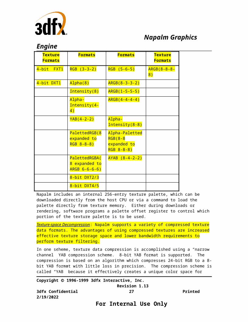
Napalm Graphics Engine
5. VGA Register Set
5.1 Overview of the Napalm VGA ControllerThe Napalm VGA core supports all standard VGA modes with full backward compatibility. This allows the 3D controller to be able to share the frame buffer with the 2D controller, thereby saving total solution cost.
In addition to the legacy VGA, Napalm also supports Vesa BIOS extensions. This is accomplished by extending the standard register set and implementing a flexible memory aperture such that VBE applications can page select memory through the standard VGA address space.
5.2 Using VGA Registers When Napalm is not the Primary VGAFor systems not requiring VGA or a VGA device already exists, Napalm allows the use of the VGA registers in an extended fashion. In this mode, VGA registers are not decoded in legacy VGA space, but in relocatable IO and memory space.
Napalm should be powered on with the device type set to ‘Multimedia Device’ through the strapping registers. Napalm will not respond to any legacy I/O or memory space. In order to use the VGA registers, Napalm should be set up to be a motherboard device (VGAINIT0 bit 8), and the IO base + 0xc3 bit 0 should be set to 1.
In this configuration, all of the VGA registers (except 0x46e8 and 0x0102) are available by truncating the leading ‘0x03’ from the legacy address, and adding that address to the I/O base address.
Note that in this configuration, however, memory is not accessible through the VGA aperture.
5.3 Locking VGA Timing for Virtualized ModesWhen running VGA applications in a window, it is possible to restrict changes to the VGA timing registers set. This is accomplished by setting the lock bits in vgaInit1. The locks prevent applications from changing the values in the associated registers.
5.4 Setting VGA Timing for Video 2 Pixels per Clock ModeFor extended resolutions that run at frequencies greater than 135Mhz, it is required that the Video Unit be placed in a 2 pixel per clock mode. This implies that the video clock is divided by 2 (see dacMode). Since the clock is running at half the frequency, all horizontal timing registers should also be divided in half.
Note: All horizontal video timing must be divisible by 16 pixels.
Copyright 1996-1999 3dfx Interactive, Inc. Revision 1.133dfx Confidential 27 Printed 5/7/2023
For Internal Use Only

Napalm Graphics Engine
VGA Registers
This section outlines the compatible VGA register set followed by a brief description of their operation.
PORT INDEX Register Name0x3B4/0x3D4 - CRTC Index Register0x3B5/0x3D5 0x0 Horizontal Total0x3B5/0x3D5 0x1 Horizontal Display Enable End0x3B5/0x3D5 0x2 Start Horizontal Blanking0x3B5/0x3D5 0x3 End Horizontal Blanking0x3B5/0x3D5 0x4 Start Horizontal Retrace0x3B5/0x3D5 0x5 End Horizontal Retrace0x3B5/0x3D5 0x6 Vertical Total0x3B5/0x3D5 0x7 Overflow0x3B5/0x3D5 0x8 Preset Row Scan0x3B5/0x3D5 0x9 Maximum Scan Line0x3B5/0x3D5 0xA Cursor Start0x3B5/0x3D5 0xB Cursor End0x3B5/0x3D5 0xC Start Address High0x3B5/0x3D5 0xD Start Address Low0x3B5/0x3D5 0xE Cursor Location High0x3B5/0x3D5 0xF Cursor Location Low0x3B5/0x3D5 0x10 Vertical Retrace Start0x3B5/0x3D5 0x11 Vertical Retrace End0x3B5/0x3D5 0x12 Vertical Display Enable End0x3B5/0x3D5 0x13 Offset0x3B5/0x3D5 0x14 Underline Location0x3B5/0x3D5 0x15 Start Vertical Blank0x3B5/0x3D5 0x16 End Vertical Blank0x3B5/0x3D5 0x17 CRTC Mode Control0x3B5/0x3D5 0x18 Line Compare0x3B5/0x3D5 0x1A Horizontal Extension Register0x3B5/0x3D5 0x1B Vertical Extension Register0x3B5/0x3D5 0x1C Extension Byte 0/ PCI Configuration0x3B5/0x3D5 0x1D Extension Byte 10x3B5/0x3D5 0x1E Extension Byte 20x3B5/0x3D5 0x1F Extension Byte 30x3B5/0x3D5 0x22 Latch Read Back0x3B5/0x3D5 0x24 Attribute Controller Index/Data State
CRTC Register Set
Read Port Write Port Register Name
Copyright 1996-1999 3dfx Interactive, Inc. Revision 1.133dfx Confidential 28 Printed 5/7/2023
For Internal Use Only
Napalm Graphics Engine 0x3CC 0x3C2 Miscellaneous Output0x3C2 -- Input Status Register 00x3BA/0x3DA -- Input Status Register 10x3CA 0x3BA/0x3DA Feature Control0x3C3 0x3C3 Motherboard Enable-- 0x46E8 Adapter Enable0x102 0x102 Subsystem Enable
General Register Set
PORT INDEX Register Name0x3C4 - Sequencer Index Register0x3C5 0x0 Reset0x3C5 0x1 Clocking Mode0x3C5 0x2 Map Mask0x3C5 0x3 Character Map Select0x3C5 0x4 Memory Mode
Sequencer Register Set
PORT INDEX Register Name0x3CE - Graphics Controller Index Register0x3CF 0x0 Set/Reset0x3CF 0x1 Enable Set/Reset0x3CF 0x2 Color Compare0x3CF 0x3 Data Rotate0x3CF 0x4 Read Map Select0x3CF 0x5 Graphics Mode0x3CF 0x6 Miscellaneous0x3CF 0x7 Color Don't Care0x3CF 0x8 Bit Mask
Graphics Controller Register Set
PORT INDEX Register Name0x3C0 0x0-0xF Palette Registers0x3C0 0x10 Attribute Mode Control Register0x3C0 0x11 Over Scan Control Register0x3C0 0x12 Color Plane Enable Register0x3C0 0x13 Horizontal PEL Panning Register0x3C0 0x14 Color Select Register
Attribute Controller Register Set
PORT Register Name0x3C6 Pixel Mask0x3C7 Read Index
Copyright 1996-1999 3dfx Interactive, Inc. Revision 1.133dfx Confidential 29 Printed 5/7/2023
For Internal Use Only
Napalm Graphics Engine 0x3C7 Read Status0x3C8 Write Index0x3C9 Data
RAMDAC Register Set
Copyright 1996-1999 3dfx Interactive, Inc. Revision 1.133dfx Confidential 30 Printed 5/7/2023
For Internal Use Only

Napalm Graphics Engine
5.5 General Registers:
5.5.1 Input Status 0 (0x3C2)Bit R/W Description7 R Interrupt Status. When its value is “1”, denotes that an interrupt is pending.6:5 R Feature Connector. These 2 bits are readable bits from the feature connector.4 R Sense. This bit reflects the state of the DAC monitor sense logic.3:0 R Reserved. Read back as 0.
Data written to port 0x3C2 is stored in the Miscellaneous Output Register (0x3CC).
5.5.2 Input Status 1 (0x3BA/0x3DA)Bit R/W Description7:6 R Reserved. These bits read back 0.5:4 R Display Status. These 2 bits reflect 2 of the 8 pixel data outputs from the Attribute
controller, as determined by the Attribute controller index 0x12 bits 4 and 5.3 R Vertical sync Status. A “1” indicates vertical retrace is in progress.2:1 R Reserved. These bits read back 0x2.0 R Display Disable. When this bit is 1, either horizontal or vertical display end has occurred,
otherwise video data is being displayed.
5.5.3 Feature Control Write (0x3BA/0x3DA)Bit R/W Description7:4 - Reserved3 W Vertical Sync Select2 - Reserved1:0 W Feature Control
5.5.4 Feature Control Read (0x3CA)Bit R/W Description7:6 R Reserved5:4 R Video Status. Reads back two bits of the VGA video stream. See 0x3c0, index 0x12, bits
5:4.3 R Vertical Sync Select2 R Reserved1:0 R Feature Control
Copyright 1996-1999 3dfx Interactive, Inc. Revision 1.133dfx Confidential 31 Printed 5/7/2023
For Internal Use Only
Napalm Graphics Engine 5.5.5 Miscellaneous Output (0x3CC)BIT R/W Description7 R Vertical Sync Polarity (0 = positive, 1= negative).6 R Horizontal Sync Polarity (0 = positive, 1= negative).5 R Page Select. When in Odd/Even mode Select High 64k bank if set.4 R Reserved3:2 R Clock Select1 R Ram Enable (1= Enable)0 R CRTC I/O Address. (1 = Color. Base Address=0x3D?; 0 = Mono. Base Address=0x3B?).
Data is written to this register via port 0x3C2. Bits 6-7 also indicate the number of lines on the display, while bit 3-2 select the video clock frequency.
5.5.6Motherboard
Enable (0x3C3)Bit R/W Description7:1 R Reserved0 R/W Video Subsystem enable
5.5.7 Adapter Enable (0x46E8)Bit R/W Description7:5 R Reserved4 W Setup Mode3 W Video Subsystem Enable2:0 R ROM Bank Address - Unused.
5.5.8 Subsystem Enable (0x102)Bit R/W Description7:1 R Reserved0 W Global Subsystem enable
Copyright 1996-1999 3dfx Interactive, Inc. Revision 1.133dfx Confidential 32 Printed 5/7/2023
For Internal Use Only
[3:2] Frequency0 25.175 Mhz1 28.322 Mhz2 50 Mhz3 Programmable PLL.
[7:6] Displayed Lines0 Reserved1 4002 3503 480

Napalm Graphics Engine
5.6 CRTC Registers:The CRTC registers are responsible for the video timing on Napalm. By default, Napalm is a 100% compatible VGA. However, Napalm can also be set up to drive much larger resolutions than that allowed by the VGA standard.
Horiz
onta
l Bor
der
Vertical Border
Vertical Border
Horiz
onta
l Bla
nk
Horiz
onta
l Bla
nk
Horiz
onta
l Bor
der
Vertical Blank
Vertical Retrace
Vertical Blank
Horiz
onta
l Ret
race
Horizontal Total
Horzontal Retrace Start
Horzontal Display EndHorzontal Blanking Start
Active Display Area
Horzontal Retrace EndHorzontal Blanking End
Verti
cal D
ispla
y En
dVe
rtica
l Bla
nkin
g St
art
Verti
cal R
etra
ce S
tart
Verti
cal R
etra
ce E
ndVe
rtica
l Bla
nkin
g En
dVe
rtica
l Tot
al
Copyright 1996-1999 3dfx Interactive, Inc. Revision 1.133dfx Confidential 33 Printed 5/7/2023
For Internal Use Only
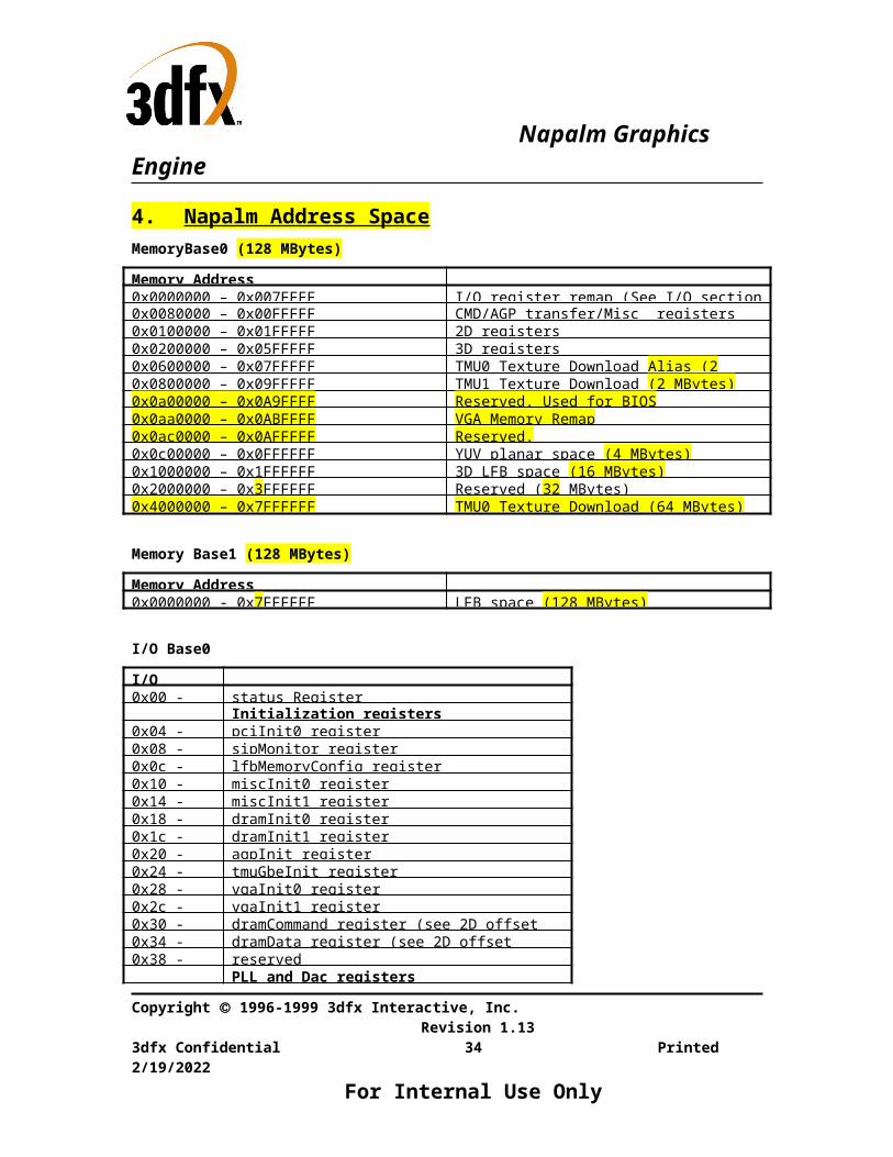
Napalm Graphics Engine The following chart indicates the bit locations for the timing registers.
10 9 8 7 6 5 4 3 2 1 0Horizontal Total 1A[0] 0 [7] 0[6] 0[5] 0[4] 0[3] 0[2] 0[1] 0[0]
Active End 1A[2] 1[7] 1[6] 1[5] 1[4] 1[3] 1[2] 1[1] 1[0]
Start Blank 1A[4] 2[7] 2[6] 2[5] 2[4] 2[3] 2[2] 2[1] 2[0]
End Blank 1A[5] 5[7] 3[4] 3[3] 3[2] 3[1] 3[0]
Start Sync 1A[6] 4[7] 4[6] 4[5] 4[4] 4[3] 4[2] 4[1] 4[0]
End Sync 1A[7] 5[4] 5[3] 5[2] 5[1] 5[0]
Vertical Total 1B[0] 7[5] 7[0] 6[7] 6[6] 6[5] 6[4] 6[3] 6[2] 6[1] 6[0]
Active End 1B[3] 7[6] 7[1] 12[7] 12[6] 12[5] 12[4] 12[3] 12[2] 12[1] 12[0]
Blank Start 1B[4] 9[5] 7[3] 15[7] 15[6] 15[5] 15[4] 15[3] 15[2] 15[1] 15[0]
Blank End 16[7] 16[6] 16[5] 16[4] 16[3] 16[2] 16[1] 16[0]
Sync Start 7[7] 7[2] 10[7] 10[6] 10[5] 10[4] 10[3] 10[2] 10[1] 10[0]
Sync End 11[3] 11[2] 11[1] 11[0]
5.6.1 CRTC Index Register (0x3B4/0x3D4)
This register provides index information for any subsequent accesses to 0x3B5/0x3D5.
Bit R/W Description7:6 R Reserved5:0 R/W CRTC Index Register.
5.6.2 Index 0x0-Horizontal Total (0x3B5/0x3D5)This register defines the total width of the display in character clocks, including retrace time, minus 5. Bit 8 of this register is found in the Horizontal Extension Register (index 0x1A) bit 0.
Bit R/W Description7:0 R/W Total Horizontal Character Count less 5.
The 5 character clocks are reserved to provide adequate prefetch time for the beginning data on the first line.
5.6.3 Index 0x1-Horizontal Display Enable End (0x3B5/0x3D5)This register defines the total number of visible horizontal characters on the display, minus one. Bit 8 of this register is found in the Horizontal Extension Register (index 0x1A) bit 2.
Bit R/W Description7:0 R/W Display Active Characters -1.
Copyright 1996-1999 3dfx Interactive, Inc. Revision 1.133dfx Confidential 34 Printed 5/7/2023
For Internal Use Only

Napalm Graphics Engine 5.6.4 Index 0x2-Start Horizontal Blanking (0x3B5/0x3D5)Horizontal blanking begins when the horizontal character counter reaches this character clock value. Bit 8 of this register is found in the Horizontal Extension Register (index 0x1A) bit 4.
Bit R/W Description7:0 R/W Start Horizontal Blanking
5.6.5 Index 0x3-End Horizontal Blanking (0x3B5/0x3D5)Bit R/W Description7 R/W Compatibility Read. When this bit is set to ‘1’ Vertical Sync Start and Vertical Sync End
are both readable and writeable. When set to ‘0’ these registers are still writeable, but not readable.
6:5 R/W Display Enable Signal Skew Control. These bits define the display enable signal skew time in relation to horizontal synchronization pulses.
4:0 R/W End Horizontal Blanking. End Horizontal Blank signal width is determined as the value of start blanking register plus W in character clocks. The least significant five bits are programmed in this register, while the most significant bit is the End Horizontal Retrace Register (Index 0x05) bit 7.
5.6.6 Index 0x4-Start Horizontal Sync (0x3B5/0x3D5)This register contains the character count at which horizontal sync output pulse becomes active. Bit 8 of this register is found in the Horizontal Extension Register (index 0x1A) bit 6.
Bit R/W Description7:0 R/W Start Horizontal Sync Character Count.
5.6.7 Index 0x5-End Horizontal Sync (0x3B5/0x3D5)Bit R/W Description7 R/W Horizontal Blank Overflow Bit 5. MSB (bit 5) of End Horizontal Blanking Register6:5 R/W Horizontal Sync Skew. These bits define the number of character clocks the horizontal
Sync signal is skewed.4:0 R/W End Horizontal Sync Pulse Width “W”. Start retrace register value is added to the
character count for width W. The least significant five bits are programmed in this register. When the Start Horizontal Retrace Register value matches these five bits, the horizontal retrace signal is turned off.
Copyright 1996-1999 3dfx Interactive, Inc. Revision 1.133dfx Confidential 35 Printed 5/7/2023
For Internal Use Only
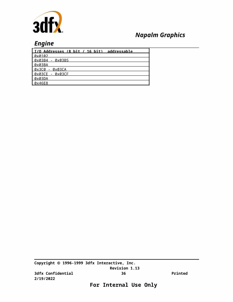
Napalm Graphics Engine
5.6.8 Index 0x6-Vertical Total (0x3B5/0x3D5)The least significant eight bits of a ten bit count of raster scan lines for a display frame less 2. Time for vertical retrace, and vertical sync are also included. The ninth and tenth bits of this count are loaded into the Vertical Overflow Register (Index 0x7) bit 0 and bit 5 respectively. Bit 8 of this register is found in the Horizontal Extension Register (index 0x1B) bit 0.
Bit R/W Description7:0 R/W Raster Scan Line Total Less 2.
5.6.9 Index 0x7-Overflow (0x3B5/0x3D5)This register contains ‘Overflow’ bits from other CRTC registers.
Bit R/W Description Base Index7 R/W Vertical Sync Start Bit 9. 0x106 R/W Vertical Display Enable End Bit 9. 0x125 R/W Vertical Total Bit 9. 0x64 R/W Line Compare Bit 8. 0x183 R/W Start Vertical Blank Bit 8. 0x152 R/W Vertical Retrace Start Bit 8. 0x101 R/W Vertical Display Enable End Bit 8. 0x120 R/W Vertical Total Bit 8. 0x6
5.6.10 Index 0x8-Preset Row Scan (0x3B5/0x3D5)BIT R/W Description7 R Reserved.6:5 R/W Byte Panning Control. These bits allow up to 3 bytes to be panned in modes programmed
as multiple shift modes.4:0 R/W Preset Row Scan Count. These bits preset the vertical row scan counter once after each
vertical retrace. This counter is incremented after each horizontal retrace period, until the maximum row scan count is reached. When maximum row scan count is reached, the counter is cleared. This register can be used for smooth vertical scrolling of text.
Copyright 1996-1999 3dfx Interactive, Inc. Revision 1.133dfx Confidential 36 Printed 5/7/2023
For Internal Use Only
6 5 Left Shift0 0 0 Pixels0 1 8 Pixels1 0 16 Pixels1 1 24 Pixels

Napalm Graphics Engine 5.6.11 Index 0x9-Maximum Scan Line (0x3B5/0x3D5)Bit R/W Description7 R/W Line Doubling. 0= Normal Operation. 1 = Activate line doubling. 6 R/W Line Compare. Bit 9 of the Line Compare Register (index = 0x18).5 R/W Start Vertical Blank. Bit 9 of the Start Vertical Blank Register (index = 0x15).4:0 R/W Maximum Scan Line. Maximum number of scanned lines for each row of characters. The
value programmed is the maximum number of scanned rows per character minus 1.
5.6.12 Index 0xA-Cursor Start (0x3B5/0x3D5)Bit R/W Description7:6 R Reserved. Defaults to 0.5 R/W Cursor Control. 0=Cursor on, 1= Cursor off.4:0 R/W Cursor Start Scan Line These bits specify the row scan counter value within the character
box where the cursor begins. These bits contain the value of the character row less 1. If this value is programmed with a value greater than the Cursor End Register (index = 0xB), no cursor is generated.
5.6.13 Index 0xB-Cursor End (0x3B5/0x3D5)Bit R/W Description7 R Reserved. Defaults to 0.6:5 R/W Cursor Skew Bits. Delays the displayed cursor to the right by the skew value in character
clocks e.g., 1 character clock skew moves the cursor right by 1 position on the screen.4:0 R/W Cursor End Scan Line. These bits specify the last row scan counter value within the
character box during which the cursor is active. If this value is less than the cursor start value, no cursor is displayed.
5.6.14 Index 0xC-Start Address High (0x3B5/0x3D5)Eight high order bits of the 16 bit video memory address, used for screen refresh. The low order eight bit register is at index 0xD.
Bit R/W Description7:0 R/W Display Screen Start Address Upper Byte Bits.
5.6.15 Index 0xD-Start Address Low (0x3B5/0x3D5)The lower order eight bits of the 16 bit video memory address.
Bit R/W Description7:0 R/W Start Address Low Byte.
Copyright 1996-1999 3dfx Interactive, Inc. Revision 1.133dfx Confidential 37 Printed 5/7/2023
For Internal Use Only
Napalm Graphics Engine 5.6.16 Index 0xE-Cursor Location High (0x3B5/0x3D5)The eight higher order bits of 16 bit cursor location in VGA modes. For the lower order eight bits, see the Cursor Location Low Register at index 0xF.
Bit R/W Description7:0 R/W Cursor Address Upper Byte Bits.
5.6.17 Index 0xF-Cursor Location Low (0x3B5/0x3D5)Bit R/W Description7:0 R/W Cursor Address Lower Byte Bits. The lower order eight bits of the 16 bit video memory
address.
5.6.18 Index 0x10-Vertical Retrace Start (0x3B5/0x3D5)The lower eight bits of the ten bit Vertical Retrace Start Register. Bits 8 and 9 are located in the Overflow Register (index = 0x7). Bit 10 is in the Vertical Extension Register (index 0x1B) bit 6.
Bit R/W Description7:0 R/W Vertical Sync Start Pulse Lower Eight Bits.
5.6.19 Index 0x11-Vertical Retrace End (0x3B5/0x3D5)Bit R/W Description7 R/W CRTC Registers Write Protect. When this bit is 0, writes to CRT index registers 0x0 to
0x7 are enabled. When this bit is 1, writes to CRT Controller index registers in the range of index 0x0 to 0x7 are protected except line compare bit 4 in the Overflow Register 0x7.
6 R/W DRAM Refresh/Horizontal Scan Line. Historically, this register selected DRAM refresh cycles per horizontal scan line. This function is not implemented.
5 R/W Enable Vertical Retrace Interrupt. (0=Enable, 1= Disable) 4 R/W Clear Vertical Retrace Interrupt. (0=Clear Vertical retrace interrupt, 1= Allow an interrupt
to be generated after the last displayed scan of the frame has occurred (i.e., the start of the bottom border).
3:0 R/W Vertical Retrace End. This register specifies the scan count at which vertical sync becomes inactive. For retrace signal pulse width W, add scan counter for W to the value of the Vertical Retrace Start Register. The 4 bit result is written in the Vertical Retrace End Register.
5.6.20 Index 0x12-Vertical Display Enable End (0x3B5/0x3D5)This register specifies the eight lower bits of ten bit register that defines where the active display frame ends. The programmed count is in scan lines minus 1. Bit 8 and 9 are in the Overflow Register (index 0x7) at bit positions 1 and 6 respectively. Bit 10 is in the Vertical Extension Register (index 0x1b) bit 2.
Bit R/W Description7:0 R/W Vertical Display Enable End Lower Eight Bits.
Copyright 1996-1999 3dfx Interactive, Inc. Revision 1.133dfx Confidential 38 Printed 5/7/2023
For Internal Use Only

Napalm Graphics Engine
5.6.21 Index 0x13-Offset (0x3B5/0x3D5)This register specifies the width of display memory in terms of an offset from the current row start address to the next character row. The offset value is a word address adjusted for word or double word display memory access.
Bit R/W Description7:0 R/W Logical Line Screen Width.
5.6.22 Index 0x14-Underline Location (0x3B5/0x3D5)Bit R/W Description7 R Reserved.6 R/W Double Word Mode. (0 = Display memory addressed for byte or word access. 1= Display
memory addressed for double word access).5 R/W Count By 4 For Double Word Access. (0= Memory address counter clocked for byte or
word access, 1 = Memory address counter is clocked at the character clock divided by 4.)4:0 R/W Underline Location. These bits specify the row scan counter value within a character
matrix where under line is to be displayed. Load a value 1 less than the desired scan line number.
5.6.23 Index 0x15-Start Vertical Blank (0x3B5/0x3D5)The lower eight bits of the ten bit Start Vertical Blank Register. Bit 8 is in the Overflow Register (index = 0x7) and bit 9 is in the Maximum Scan Line Register (index = 0x9). The ten bit value is reduced by 1 from the desired scan line count where the vertical blanking signal starts.
Bit R/W Description7:0 R/W Start Vertical Blank Lower Eight Bits.
5.6.24 Index 0x16-End Vertical Blank (0x3B5/0x3D5)Bit R/W Description7:0 R/W Vertical Blank Inactive Count.
End Vertical Blank is an 8 bit value calculated as follows:End Vertical Blank = (Start Vertical Blank - 1) + (Vertical Blank signal width in scan lines).
Copyright 1996-1999 3dfx Interactive, Inc. Revision 1.133dfx Confidential 39 Printed 5/7/2023
For Internal Use Only
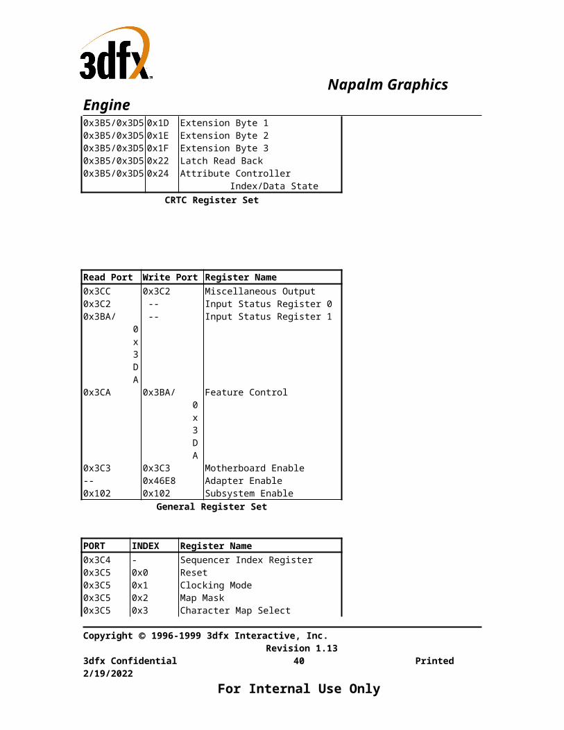
Napalm Graphics Engine
5.6.25 Index 0x17-CRTC Mode Control (0x3B5/0x3D5)Bit R/W Description7 R/W Sync Enable. (0= retrace outputs disabled, 1= retrace outputs enabled)6 R/W Word or Byte Mode. (0= Word address mode, 1= Byte address mode)5 R/W Address Wrap. In word address mode, setting this bit to 0 enables bit 13 to appear at
MAO, otherwise in byte address mode bit 0 appears on MAO. Setting this bit to 1 selects MA15 for odd/even mode.
4 R Reserved.3 R/W Count by 2 (0 = Character clock increments memory address counter, 1= Character clock
divided by 2 increments the address counter).2 R/W Horizontal Retrace Clock Rate Select For Vertical Timing Counter. 0= Normal, 1= Selects
horizontal retrace clock rate divided by 2.)1 R/W Select Row Scan Counter.0=Selects row scan counter bit 1 as output at MA14 address
pin.1 Selects bit 14 of the CRTC address counter as output at MA14 pin.0 R/W 6845 CRT Controller compatibility mode support for CGA operation. 0 = Row scan
address bit 0 is substituted for memory address bit 13 at MA13 output pin during active display time. 1=Enable memory address pin 13 to be output at MA13 address pin.
5.6.26 Index 0x18-Line Compare (0x3B5/0x3D5)Bit R/W Description7:0 R/W Line Compare Lower Eight Bits. Lower eight bits of the ten bit Scan Line Compare
Register. Bit 8 is in the Overflow Register (index = 0x7) and bit 9 is in the Maximum Scan Line Register (index = 0x9). When the vertical counter reaches this value, the internal start of the line counter is cleared.
5.6.27 Index 0x1A-Horizontal Extension Register (0x3B5/0x3D5)This register is an extension of the VGA core in order to increase the total horizontal resolution available to Napalm. This register is only active when VGAINIT0 bit 6 is ‘1’.
Bit R/W Description Base Index7 R/W Horizontal Retrace End bit 5. -6 R/W Horizontal Retrace Start bit 8 0x45 R/W Horizontal Blank End bit 6. -4 R/W Horizontal Blank Start bit 8. 0x33 R/W Reserved. -2 R/W Horizontal Display Enable End bit 8. 0x11 R/W Reserved. -0 R/W Horizontal Total bit 8. 0x0
Copyright 1996-1999 3dfx Interactive, Inc. Revision 1.133dfx Confidential 40 Printed 5/7/2023
For Internal Use Only
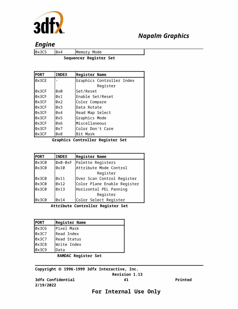
Napalm Graphics Engine 5.6.28 Index 0x1B-Vertical Extension Register (0x3B5/0x3D5)This register is an extension of the VGA core in order to increase the total Vertical resolution available to Napalm. This register is only active when VGAINIT0 bit 6 is ‘1’.
Bit R/W Description Base Index7 R/W Reserved -6 R/W Vertical Retrace Start bit 10 0x105 R/W Reserved. -4 R/W Vertical Blank Start bit 10. 0x153 R/W Reserved. -2 R/W Vertical Display Enable End bit 10 0x121 R/W Reserved. -0 R/W Vertical Total bit 10. 0x6
5.6.29 Index 0x1C-PCI Config/Extension Byte 0 (0x3B5/0x3D5)On power up, Napalm is configured to allow read back of the PCI configuration information a byte at a time through this register. In order to use this feature, first follow the standard wake up sequence. To selectively read back configuration information, write the index into this register. Data read back from this register is the configuration byte at that index.
Bit R/W Description7:0 R/W PCI Configuration/Scratch Pad Register.
The use of the extended register space is decoded as follows:
5.6.30 Index 0x1D-Extension Byte 1 (0x3B5/0x3D5)This register is only active when VGAINIT0 bit 6 is ‘1’
Bit R/W Description7:0 R/W Scratch Pad Register.
Copyright 1996-1999 3dfx Interactive, Inc. Revision 1.133dfx Confidential 41 Printed 5/7/2023
For Internal Use Only
VGAINIT0 7 6 Description0 0 Allow Configuration data to be read back from PCI
(Indexed)0 1 Extended registers Are scratch Pad1 X Extended registers Disabled

Napalm Graphics Engine
5.6.31 Index 0x1E-Extension Byte 2 (0x3B5/0x3D5)This register is only active when VGAINIT0 bit 6 is ‘1’
Bit R/W Description7:0 R/W Scratch Pad Register.
5.6.32 Index 0x1F-Extension Byte 3 (0x3B5/0x3D5)This register is only active when VGAINIT0 bit 6 is ‘1’
Bit R/W Description7:0 R/W Scratch Pad Register.
5.6.33 Index 0x20-Vertical Counter pre-load Low (0x3B5/0x3D5)This register, in combination with index 0x20, allows the vertical counter to be pre-loaded for testing purposes. The vertical counter is pre-loaded on reset, which can be caused either through a hard reset or a soft reset. This register is only active when VGAINIT0 bit 6 is ‘1’.
Bit R/W Description7:0 R/W Scratch Pad Register.
5.6.34 Index 0x21- Vertical Counter pre-load High(0x3B5/0x3D5)This register is only active when VGAINIT0 bit 6 is ‘1’
Bit R/W Description2:0 R/W Scratch Pad Register.
5.6.35 Index 0x22-Latch Read Back (0x3B5/0x3D5)Bit R/W Description7:0 R/W Latch Data Register. This register reflects the contents of one of the four Graphics Data
Controller latches. The plane selected for read back is determined by Graphics Controller Read Map Select Register (index 0x4) bits 0 and 1.
5.6.36 Index 0x24-Attribute Controller Index/Data State (0x3B5/0x3D5)Bit R/W Description7 R Attribute Controller Index/Data State. When this is 1, the Attribute controller register is set
to ‘Data’ state. When set to 0, the Attribute controller register is set to ‘Index’ state. Reading 0x3DA will always put the Attribute Controller back to Index State.
6:0 R Reserved.
Copyright 1996-1999 3dfx Interactive, Inc. Revision 1.133dfx Confidential 42 Printed 5/7/2023
For Internal Use Only
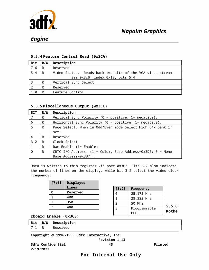
Napalm Graphics Engine 5.6.37 Index 0x26-Display Bypass/Attribute Controller Index (0x3B5/0x3D5)Bit R/W Description5 R Display Bypass. Reflects the value of the Attribute Controller index register, bit 5. 4:0 R Attribute index.
Copyright 1996-1999 3dfx Interactive, Inc. Revision 1.133dfx Confidential 43 Printed 5/7/2023
For Internal Use Only
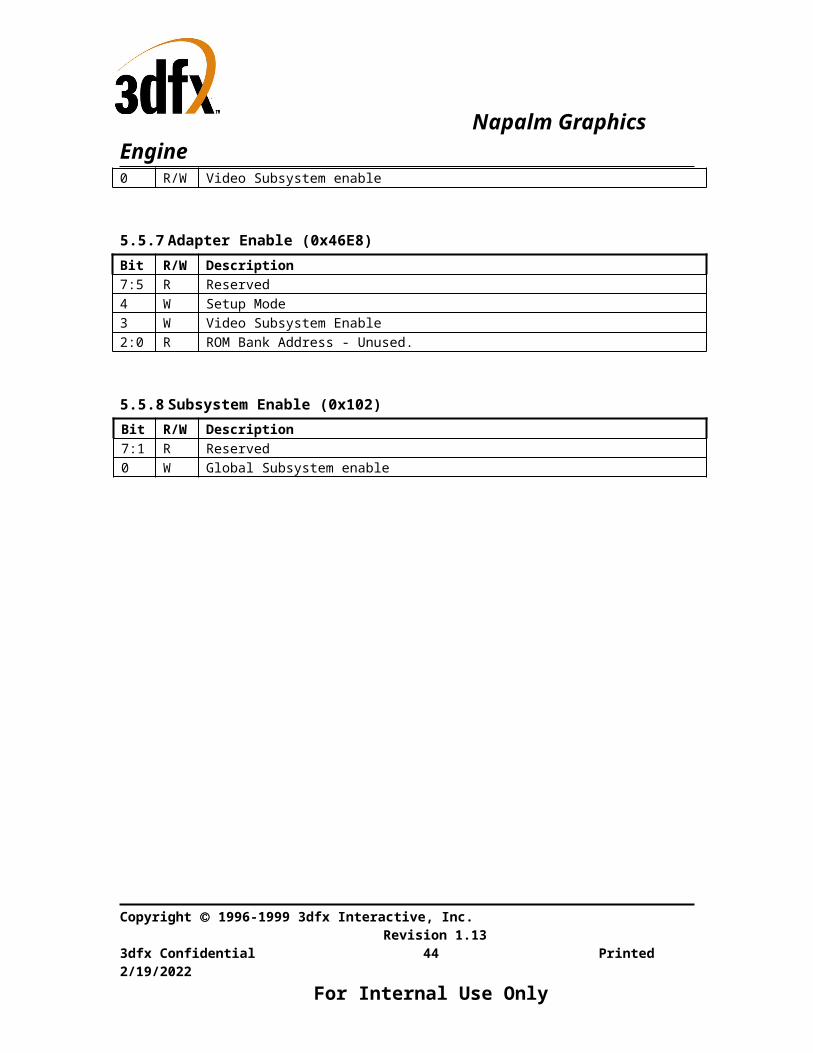
Napalm Graphics Engine
5.7 Graphics Controller Registers:
5.7.1 Graphics Controller Index Register (0x3CE)Data written to this 8 register reflects the index of the Graphics Controller register space accessed through 0x3CF.
Bit R/W Description7:4 R Reserved.3:0 R/W Index for accesses at 0x3CF.
5.7.2 Index 0-Set/Reset (0x3CF)Bit R/W Description7:4 R Reserved.3:0 R/W Set/Reset Map.
When the CPU executes display memory write with Write Mode 0 selected and the Enable Set/Reset Register (index = 0x1) activated, the eight bits of the value in this register, which have been operated on by the Mask Register, are then written to the corresponding display memory map. It is an eight fill operation. The map designations are defined below:
5.7.3 Index 1-Enable Set/Reset (0x3CF)Bit R/W Description7:4 R Reserved.3:0 R/W Enable Set/Reset Register (Index 0x0). When Write Mode 0 is selected, these bits enable
memory map access defined by the Set/Reset Register (index = 0x0), and the respective memory map is written with the Set/Reset Register value.
5.7.4 Index 2-Color Compare (0x3CF)The color compare contains the value to which all 8 bits of the corresponding memory map are compared. This comparison also occurs across all four maps, and a 1 is returned for the map positions where the bits of all four maps equal the Color Compare Register. If a system read is done with 3 = 0 for the Graphics Mode Register (index = 0x5), data is returned without comparison. Color compare map coding is shown below.
Bit R/W Description7:4 R Reserved.3:0 R/W Color Compare.
Copyright 1996-1999 3dfx Interactive, Inc. Revision 1.133dfx Confidential 44 Printed 5/7/2023
For Internal Use Only
0 Reset.1 Set.

Napalm Graphics Engine
5.7.5 Index 3-Data Rotate (0x3CF)Bit R/W Description7:5 R Reserved.4:3 R/W Function Select. Function select for any of the write mode operations defined in the
Graphics Mode Register (index = 0x5) is defined in the following table.2:0 R/W Rotate Count. These bits specify number of positions of rotation to the right and is
ineffective in write mode 2, defined by the Graphics Mode Register (index =0x5).
5.7.6 Index 4-Read Map Select (0x3CF)Bit R/W Description7:2 R Reserved.1:0 R/W Map Select. These bits select memory map in system read operations. It has no effect on
color compare read mode. In odd/even modes, the value can be 0x0 or 0x1 to select chained maps 0 & 1 or value 0x2 or 0x3 to select the chained maps 2 & 3.
5.7.7 Index 5-Graphics Mode (0x3CF)Bit R/W Description7 R Reserved.6:5 R/W Shift Mode.
00 = data is shifted out normally.01 = data is shifted out Even/Odd1x = 256 Color Mode shift
4 R/W CGA compatible Odd/Even Mode. When set to ‘1’ , Sequential addressing is as defined by bit 2 of the Memory Mode Register (index = 0x4) in the Sequencer Register. Even system addresses access maps 0 or 2 and odd system addresses access maps 1 or 3.
3 R/W Read Mode. When set to 0, System reads data from memory maps selected by Read Map Select Register (index 0x4). This setting has no effect if bit 3 of the Sequencer Memory Mode Register = 1. When set to 1, System reads the comparison of the memory maps and the Color Compare Register.
2 R Reserved.1:0 R/W Write Mode. The table on the following page defines the four write modes.
Copyright 1996-1999 3dfx Interactive, Inc. Revision 1.133dfx Confidential 45 Printed 5/7/2023
For Internal Use Only
4 3 Function0 0 Move0 1 And1 0 Or1 1 Xor

Napalm Graphics Engine
5.7.8 Index 6-Miscellaneous (0x3CF)Bit R/W Description 7:4 R Reserved.3:2 R/W Memory Map 1,0 Display memory map control into the CPU address space is shown in
the following table.1 R/W Odd/Even Mode. When set to 1, CPU address A0 is replaced by higher order address bit.
A0 is then used to select odd or even maps. A0 = 0 selects map 0 or 2, while A0 = 1 selects map 1 or 3.
0 R/W Graphics/Alphanumeric Mode. 0 = Alphanumeric mode, 1= Graphics mode.
5.7.9 Index 7-Color Don’t Care (0x3CF)Bit R/W Description7:4 R Reserved.3:0 R/W Memory Map Color Compare Operation. 1=Enable, 0 = Disable.
5.7.10 Index 8-Mask (0x3CF)Mask operation applies simultaneously to all the four maps. In Write Modes 0 and 2, this register provides selective changes to any stored in the system latches during processor writes. Data must be first latched by reading the addressed byte. After setting the Mask Register, new data is written to the same byte in a subsequent operation. Mask operation is applicable to any data written by the processor.
Bit R/W Description7:0 R/W Mask. 0 = Mask, 1 = Disable mask.
Copyright 1996-1999 3dfx Interactive, Inc. Revision 1.133dfx Confidential 46 Printed 5/7/2023
For Internal Use Only
Bits 1:0
Write Mode
Description
00 0 CPU or data from the Set/Reset Register is written to graphics memory.
01 1 Latch data is written to graphics memory10 2 Plane n is filled with data bit n11 3 The addressed byte in each plane is filled with the value of the
corresponding bits in the Set/Reset Register (index 0x0). The Enable Set/Reset Register (index 0x1) has no effect. Rotated CPU data is logically ANDed with the Mask Register (index 0x8).
3 2 Physical Address Size Typical Usage0 0 0xA0000 128K None0 1 0xA0000 64K EGA/VGA/Extended Graphics Modes1 0 0xB0000 32K Monochrome Text Modes1 1 0xB8000 32K Color Text / CGA Graphics Modes
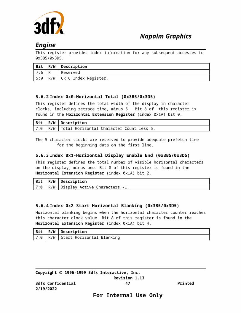
Napalm Graphics Engine
5.8 Attribute Registers
5.8.1 Attribute Index Register (0x3C0)The Attribute Index Register has an internal flip-flop, rather than an input bit, which controls the selection of the Address and Data Registers. Reading the Input Status Register 1 (port = 0x3BA/0x3DA) clears the flip flop and selects the Address Register, which is read through address 0x3C1 and written at address 0x3C0. Once the Address Register has been loaded with an index, the next write operation to 0x3C0 will load the Data Register. The flip-flop toggles between the Address and the Data Registers after every write to address hex 0x3C0, but does not toggle for reads to address 0x3C1.
Bit R/W Description 7:6 R Reserved.5 R/W Palette Address Source. (0=Disable palette outputs, 1=Enable palette outputs.)4:0 R/W Attribute Controller Index Register Address Bits
5.8.2 Index 0x0 through 0xF-Palette Registers (0x3C0/3C1)The Palette Registers are effectively a lookup table 6 bits wide by 16 levels deep. The purpose of this lookup table is to allow dynamic color mapping from the original video data stream. The palette provides a translation from 4 bits to 6 bits of data. The palette output data is either combined with the Color Select Register (index 0x14), or two the result of two shifts are appended together, resulting in an 8 bit video stream.
Bit R/W Description 7:6 R Reserved.5:0 R/W Palette Pixel Colors.
5.8.3 Index 10-Attribute Mode Control Register (0x3C0)Bit R/W Description7 R/W VID5, VID4 Select (0=Use palette outputs, 1=use Color select Register index 0x14.)6 R/W Pixel Width (0= one pixel every VCLK, 1 = one pixel every 2 VCLK)5 R/W Pixel Panning Compatibility. (0=Enable Pixel Pan on line compare, 1 = disable on line
compare)4 R Reserved.3 R/W Background Intensity/Blink Selection. (0= MSB of attribute is background color, 1= MSB
of attribute is blink)2 R/W Line Graphics Character Code. Setting this bit to 0 forces ninth dot to be the same color as
background in line graphics character codes. Setting this bit to 1 forces the ninth dot character to be identical to the eighth character dot. Set this to zero for character fonts that do not utilize line graphics character codes.
1 R/W Mono/Color Emulation. (0=Color, 1 = Mono)0 R/W Graphics/Alphanumeric Mode Enable. (0=alphanumeric, 1= graphics)
Copyright 1996-1999 3dfx Interactive, Inc. Revision 1.133dfx Confidential 47 Printed 5/7/2023
For Internal Use Only
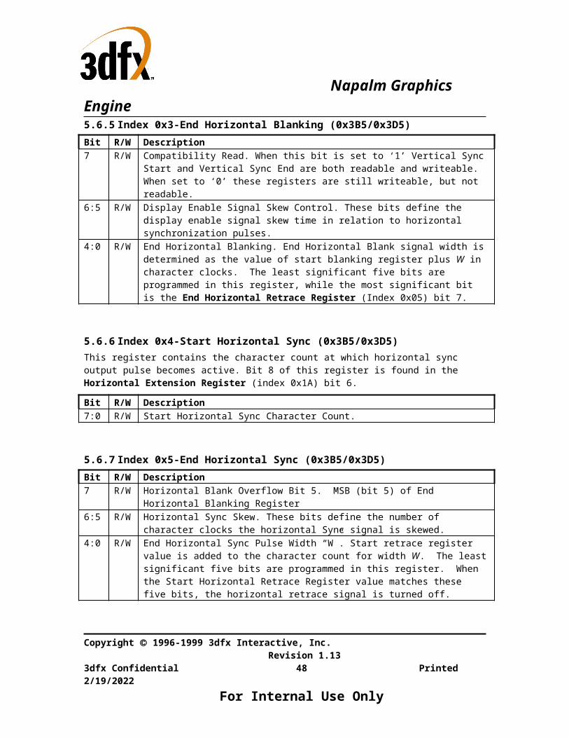
Napalm Graphics Engine 5.8.4 Index 11-Over Scan Control Register (0x3C0)This register determines the over scan or border color. For monochrome displays, this register is set to 0.
Bit R/W Description7:0 R/W Over Scan/Border Color
5.8.5 Index 12-Color Plane Enable Register (0x3C0)Bit R/W Description7:6 R Reserved.5:4 R/W Video Status Control. These bits select 2 out of 8 color outputs which can be read by the
Input Status Register 1 (port = 0x3BA/0x3DA) bits 4 and 5.3:0 R/W Color Plane Enable. Setting a bit to 0 disables the respective color plane(s).
5.8.6 Index 13-Horizontal Pixel Panning Register (0x3C0)These bits select pixel shift to the left horizontally. For 9 dots/character modes, up to 8 pixels can be shifted horizontally to the left. Likewise, for 8 dots/character up to 7 pixels can be shifted horizontally to the left. For 256 color, up to 3 position pixel shifts can occur.
Bit R/W Description7:4 R Reserved.3:0 R/W Horizontal Pixel Panning. See table.
5.8.7 Index 14-Color Select Register (0x3C0)Bit R/W Description7:4 R Reserved.3:2 R/W Color Value MSB. Two most two significant bits of the eight digit color value for the
video DAC. They are normally used in all modes except 256 color graphics.1:0 R/W Substituted Color Value Bits. These bits can be substituted for VID5 an VID4 output by
the Attribute Controller palette registers, to create eight color value. They are selected by the Attribute Controller Mode Control Register (index = 0x10).
Copyright 1996-1999 3dfx Interactive, Inc. Revision 1.133dfx Confidential 48 Printed 5/7/2023
For Internal Use Only
Bits [3:0] 9 bit text 256 color Other 0x0 1 0 00x1 2 ½ 10x2 3 1 20x3 4 1 ½ 30x4 5 2 40x5 6 2 ½ 50x6 7 3 60x7 8 3 ½ 70x8-0xf 0 -1 -1

Napalm Graphics Engine
5.9 Sequencer Registers
5.9.1 Sequencer Index Register (0x3c4)Bit R/W Description 7:0 R/W Index for accesses at 0x3c5.
5.9.2 Index 0-Reset (0x3c5)Bit R/W Description7:2 R Reserved.1 R/W Synchronous Reset. 0=Video Timing is cleared and halted. This is used to synchronize
changing the either bits 3 or 2 of the Miscellaneous Output Register. 1= Operational mode.
0 R/W Asynchronous Reset. 0=Sequencer is cleared and halted asynchronously. This bit is used to force the Sequencer into a reset state, regardless of the operation it is performing. 1=Operational mode.
5.9.3 Index 1-Clocking Mode (0x3c5)Bit R/W Description 7:6 R Reserved5 R/W Screen Off. When this bit is set to 1 the screen turned off, all requests for video FIFO
refresh are disabled, allowing additional bandwidth for other memory operations. SYNC signals remain active.
4 R/W Video Serial Shift Register Loading. When this bit is 0, serial shift registers are loaded every character or every other character clock depending on bit 2 of this register; otherwise when this bit is 1, Serial shift registers loaded every 4 th character clock (32 fetches).
3 R/W Dot Clock Selection (0= Normal dot clock selected by VCLK input frequency, 1 = Dot Clock divided by 2 (used for 320/360 pixel width display modes).
2 R/W Shift Load. This is only effective if bit 4 of this register = 0. (0=Video serializers will be loaded every character clock, 1 = Video serializers are loaded every other character clock).
1 R Reserved.0 R/W 8/9 Dot Clock. (0= 9 dot wide character clock, 1 = 8 dot wide character clock)
5.9.4 Index 2-Map Mask (0x3c5)Bit R/W Description7:4 R Reserved.3:0 R/W Map Enables. If a bit is 0, writing to the corresponding map(0-3) is disabled.
Copyright 1996-1999 3dfx Interactive, Inc. Revision 1.133dfx Confidential 49 Printed 5/7/2023
For Internal Use Only

Napalm Graphics Engine 5.9.5 Index 3-Character Map Select (0x3c5)If Sequencer Register index 4 bit 1 is 1, then the attribute byte 3 in text modes is redefined to control switching between character sets in alphanumeric modes. An attribute of 0 selects character map B, while a 1 selects character map A.
Bit R/W Description7:6 R Reserved.5 R/W Character Map A High Select. The Most Significant (MSB) of character map A along with
bits 3 and 2, select the location of character map A as shown below.4 R/W Character Map B High Select. The MSB of character map B along with bits 1 and 0, select
the location of character map B as shown below.3:2 R/W Character Map Select A. Refer to Character Map A Select table.1:0 R/W Character Map Select B. Refer to Character Map B Select table.
Copyright 1996-1999 3dfx Interactive, Inc. Revision 1.133dfx Confidential 50 Printed 5/7/2023
For Internal Use Only
Bit Map Table Location5 3 2 Selected (Maps 2 or 3)0 0 0 0 1st 8K0 0 1 1 3rd 8K0 1 0 2 5th 8K0 1 1 3 7th 8K1 0 0 4 2nd 8K1 0 1 5 4th 8K1 1 0 6 6th 8K1 1 1 7 8th 8K
Character Map A Select
Bit Map Table Location4 1 0 Selected (Maps 2 or 3)0 0 0 0 1st 8K0 0 1 1 3rd 8K0 1 0 2 5th 8K0 1 1 3 7th 8K1 0 0 4 2nd 8K1 0 1 5 4th 8K1 1 0 6 6th 8K1 1 1 7 8th 8K
Character Map B Select

Napalm Graphics Engine
5.9.6 Index 4-Memory Mode (0x3c5)Bit R/W Description7:4 R Reserved.3 R/W Chain 4 Maps. (0= Processor sequentially accesses data using map mask register, 1 = The
two lower order video memory address pins (MAO,MA1) to select the map to be addressed)
2 R/W Odd/Even. Bit 3 of this register must be 0 for this bit to be effective. (0=Odd/Even Mode, 1 = Normal)
1 R/W Extend Memory. (0= restrict size to 16/32K, 1= allow 256K).0 R Reserved
Copyright 1996-1999 3dfx Interactive, Inc. Revision 1.133dfx Confidential 51 Printed 5/7/2023
For Internal Use Only

Napalm Graphics Engine
5.10 RAMDAC Registers
5.10.1 RAMDAC Pixel Mask (0x3c6)Bit R/W Description7:0 R/W RAMDAC pixel mask
The contents of this register are logically ANDed with the output of the VGA data stream before it is presented to the RAMDAC. The value of this register has no effect on modes other than VGA.
5.10.2 RAMDAC Read Index /Read Status (0x3c7)Bit R/W Description7:0 W RAMDAC Read Index1:0 R RAMDAC State. 0 = a read operation is in effect, 3 = a write operation is in effect.
When data is written to this register, it causes the CLUT to go into a ‘Read State’. It should be followed be three consecutive reads of 0x3c9 in order to retrieve the red, green and blue values of the CLUT. This index will auto increment following the completion of the last data read. Note that only the first 256 locations of the CLUT may be accessed via this port.
When data is read from this register, bits 1:0 indicate the read/write state of the CLUT.
5.11 RAMDAC Write Index (0x3c8)Bit R/W Description7:0 R/W RAMDAC Write Index
When data is written to this register, it causes the CLUT to go into a ‘Write State’. It should be followed be three consecutive writes of 0x3c9 in order to store the red, green and blue values of the CLUT. This index will auto increment following the completion of the last data write. Note that only the first 256 locations of the CLUT may be accessed via this port.
5.11.1 RAMDAC Data (0x3c9)Bit R/W Description7:0 R/W RAMDAC palette data
This register contains the data written to the CLUT. Data in this register is either 6 bit (VGA compatible) or 8 bit, as determined by VGAINIT0 bit 2. When data is in 6 bit format, the 2 MSBs are replicated into the 2 LSBs to maintain full scale and linearity on the DAC.
Copyright 1996-1999 3dfx Interactive, Inc. Revision 1.133dfx Confidential 52 Printed 5/7/2023
For Internal Use Only
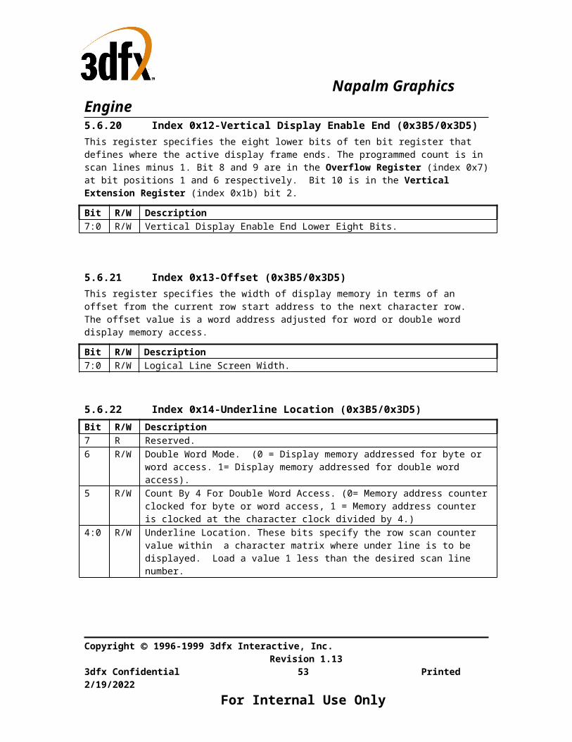
Napalm Graphics Engine 6. Accessing memory in VESA modes VGA is restricted to only see 128K of memory through 0x0A0000. This supports baseline VGA graphics modes well; however, extended resolutions and video color depths in VESA modes require use of more memory than that allowed by the VGA standard.
Access to the entire frame buffer is available in VESA modes through a method of re-mapping the 0x0A0000 host memory space into part of the video memory. Memory accessed through 0x0A0000 in VESA modes is unaffected by the settings of the Graphics Control or Sequencer Registers.
There are two aperture controls, one for reading memory and one for writing memory. This allows memory to be moved from addresses greater than 64K apart without frequently modifying the aperture pointers. Each aperture can point to video memory anywhere along a 32K boundary.
7. 2D
7.1 2D Register Map
Memory Base 0: Offset 0x0100000
Register Name Address Reg Bits R/ Description
Copyright 1996-1999 3dfx Interactive, Inc. Revision 1.133dfx Confidential 53 Printed 5/7/2023
For Internal Use Only

Napalm Graphics Engine
WStatus 0x000(0) 0x0 31:0 R Napalm status registerIntCtrl 0x004(4) 0x1 31:0 R/W Interrupt control and statusclip0Min 0x008(8) 0x2 28:0 R/W Min X & Y clip values when clip select is 0clip0Max 0x00c(12) 0x3 28:0 R/W Max X & Y clip values when clip select is 0dstBaseAddr 0x010(16) 0x4 31:0 R/W Destination base addressdstFormat 0x014(20) 0x5 17:0 R/W Destination stride and bits per pixelsrcColorkeyMin 0x018(24) 0x6 23:0 R/W Source Colorkey range (min)srcColorkeyMax 0x01c(28) 0x7 23:0 R/W Source Colorkey range (max)dstColorkeyMin 0x020(32) 0x8 23:0 R/W Destination Colorkey range (min)dstColorkeyMax 0x024(36) 0x9 23:0 R/W Destination Colorkey range (max)bresError0 0x028(40) 0xA 31:0 R/W Initial error for lines, right edges & stretch blt xbresError1 0x02c(44) 0xB 31:0 R/W Initial error for left poly edges & stretch blt yrop 0x030(48) 0xC 31:0 R/W 4 Ternary Raster operationssrcBaseAddr 0x034(52) 0xD 31:0 R/W Source base addresscommandExtra 0x038(56) 0xE 31:0 R/W Extra control bitslineStipple 0x03c(60) 0xF 31:0 R/W Monochrome pattern for lineslineStyle 0x040(64) 0x10 28:0 R/W Style register for linespattern0Alias 0x044(68) 0x11 31:0 R/W Alias to colorPattern(0)pattern1Alias 0x048(72) 0x12 31:0 R/W Alias to colorPattern(1)clip1Min 0x04c(76) 0x13 28:0 R/W Min X & Y clip values when clip select is 1clip1Max 0x050(80) 0x14 28:0 R/W Max X & Y clip values when clip select is 1srcFormat 0x054(84) 0x15 18:0 R/W Source stride and bits per pixelsrcSize 0x058(88) 0x16 28:0 R/W Height and width of source for stretch bltssrcXY 0x05c(92) 0x17 28:0 R/W Starting pixel of blt source data
Starting position for linesTop-most point for a polygon fill
colorBack 0x060(96) 0x18 31:0 R/W Background colorcolorFore 0x064(100) 0x19 31:0 R/W Foreground colordstSize 0x068(104) 0x1A 28:0 R/W Destination width and height for blts and
rectangle fillsdstXY 0x06c(108) 0x1B 28:0 R/W Starting X and Y of destination for blts
End point for linescommand 0x070(112) 0x1C 31:0 R/W 2D command mode & control bitsRESERVED 0x074(116) 0x1D 31:0 Do not writeRESERVED 0x078(120) 0x1E 31:0 Do not writeRESERVED 0x07c(124) 0x1F 31:0 Do not writelaunchArea 0x080(128)
to0x0ff(255)
0x20 to 0x3F
31:0 R Initiates 2D commands
colorPattern 0x100(256) to0x1fc(508)
0x40 to 0x7F
31:0 R/W Pattern Registers (64 entries)
Copyright 1996-1999 3dfx Interactive, Inc. Revision 1.133dfx Confidential 54 Printed 5/7/2023
For Internal Use Only
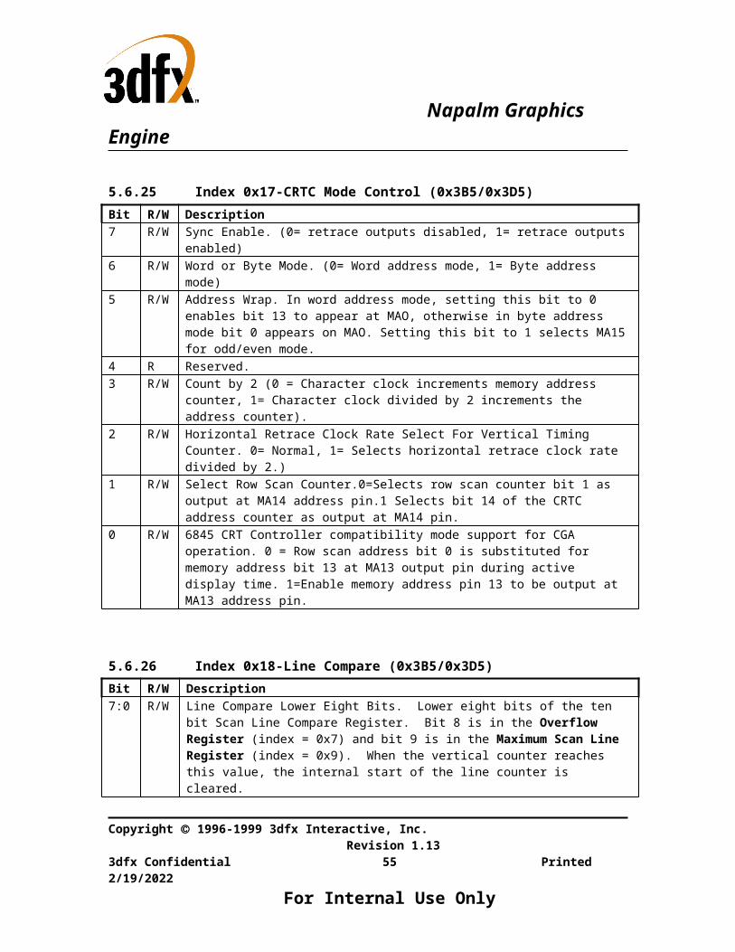
Napalm Graphics Engine
7.2 Register DescriptionsThe 2D register set is described in the sections below.
All 2D registers can be read, and all registers except for the status register are fully write-able. Reading a 2D register will always return the value that will be used if a new operation is begun without writing a new value to that register. This value will either be the last value written to the register, or, if an operation has been performed since the value was written, the value after all operations have completed.
All registers for the 2D section are unsigned unless specified otherwise.
7.2.1 status RegisterThe status register provides a way for the CPU to interrogate the graphics processor about its current state and FIFO availability. The status register is read only, but writing to status clears any Napalm generated PCI interrupts. For the definition of this register please see section XXX on PCI configuration and Initialization registers.
7.2.2 command RegisterThe command register sets the command mode for the 2D engine, as well as selecting a number of options.
Bits (3:0) set the command mode for the 2D drawing engine as shown in the table below. If bit(8) is set, the command will be initiated as soon as the command register is written. If bit(8) is cleared, drawing will be initiated by a write to the launch area. For descriptions and examples of each command, see the 2D launch area section.
Command[3:0] Command0 Nop - wait for idle1 Screen to screen blt2 Screen to screen stretch blt3 Host to screen blt4 Host to screen stretch blt5 Rectangle fill6 Line7 Polyline8 Polygon fill13 Write Sgram/Sdram Mode register14 Write Sgram Mask register15 Write Sgram Color register
Setting Bit(9) makes line drawing reversible. If this bit is set, drawing a line from point A to point B will result in the same pixels being drawn as drawing a line from point B to point A.
Bits(11:10) control the value placed in dstXY after each blt or rectangle fill command is executed. If bit(10) is 0, dst_x is unchanged. If bit(10) is 1, dst_x gets dst_x + dst_width. If bit(11) is 0, dst_y is unchanged. If bit(11) is 1, dst_y gets dst_y + dst_height.
Copyright 1996-1999 3dfx Interactive, Inc. Revision 1.133dfx Confidential 55 Printed 5/7/2023
For Internal Use Only
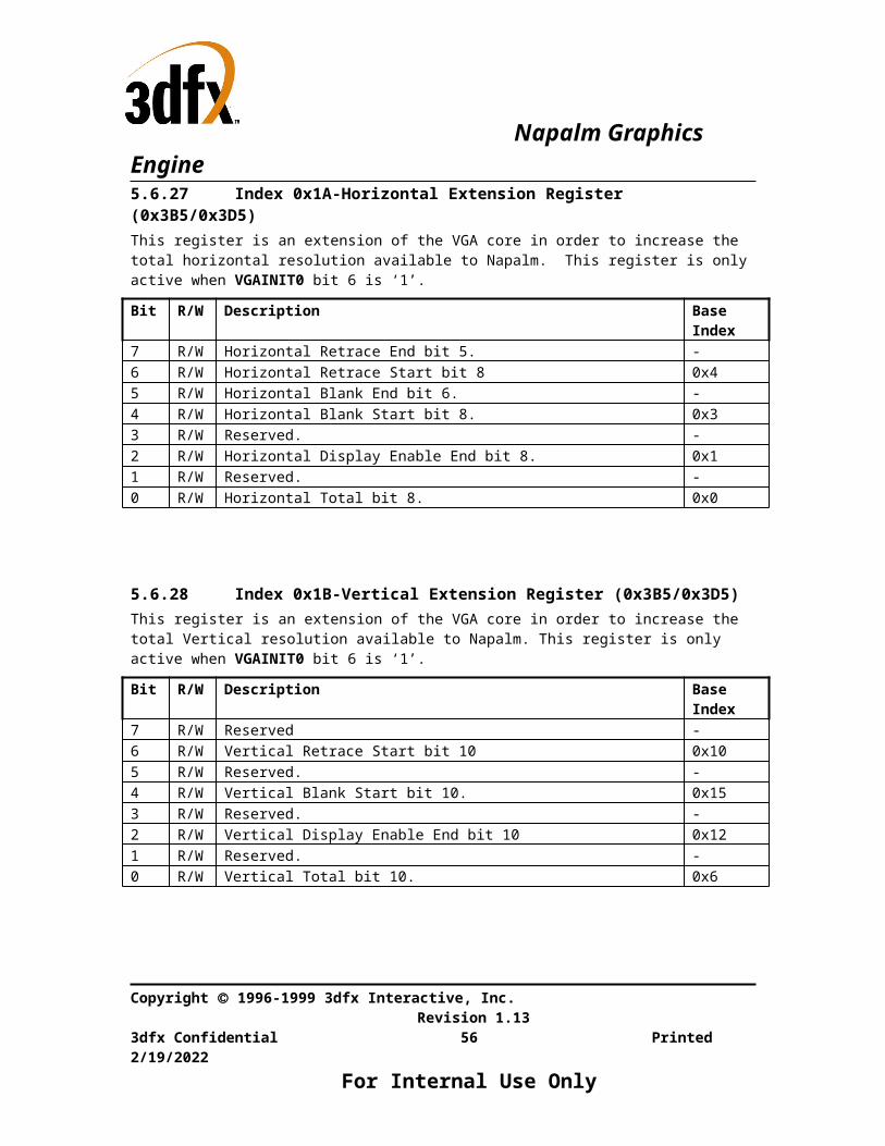
Napalm Graphics Engine Bit(12) controls whether lines are stippled or solid. If bit(12) is 0, lines will be a solid color. If bit(12) is 1, lines will either be made up of either a two color pattern using colorFore and colorBack or will be a transparent stipple using colorFore, as determined by the transparency bit - bit(16).
Bit(13) controls the format of the pattern data. If bit(13) is set to 0, the pattern must be stored in the destination format. If it is set to 1, the pattern will be stored as a monochrome bitmap; Pattern registers 0 and 1 will be used as an 8x8x1bpp pattern, which will be expanded into the destination format using the colorBack and colorFore registers. Note that if Bit(13) is set, and Bit(16) is set to indicate that monochrome data is transparent, the pattern will be used to determine pixel transparency without regard to the contents of the ROP register.
Bits(15:14) control the direction of blting during screen-to-screen copies. Note that the corner of the source and destination rectangles passed in the srcXY and dstXY registers will change depending on the blting direction. Bit(15) also controls the direction of blting for host-to-screen copies. This can be used to flip a pixel map so that the top span in host memory is drawn as the bottom span on the screen. Note that the direction bits only apply to “pure” screen to screen blits, but not to stretch blits. Also, destination and source color keying, along with color conversions, cannot be used with right to left blits.
Bit(16) controls whether monochrome source bitmaps, and monochrome patterns will be transparent or opaque. When bit(16) is 0, source bitmaps are opaque; a 0 in the bitmap will result in colorBack being written to the destination. When bit(16) is 1, source bitmaps and monochrome patterns are transparent. In this case, a 0 in the bitmap will result in the corresponding destination pixel being left unchanged.
The X and Y pattern offsets give the coordinates within the pattern of the pixel which corresponds to the destination pixel pointed to by the destination base address register. In other words, if a pattern fill is performed which covers the origin, pixel (0,0) in the destination pixel map will be written with the color in pattern pixel (x_pat_offset, y_pat_offset).
Bit(23) controls whether the clip0 or clip1 registers will be used for clipping. When bit(31) is 0, clipping values from clip0Min and clip0Max will be used, when bit(31) is 1, clipping values from clip1Min and clip1Max will be used.
Bits(31:24) contain ROP0, the ternary ROP that is used when colorkeying is disabled. For more information on ROPs, see the description of the rop register.CommandBit Description3:0 Command7:4 RESERVED8 Initiate command (1=initiate command immediately, 0 = wait for launch write)9 Reversible lines (1=reversible, 0=non-reversible)10 Increment destination x-start after blt or rectangle command (1=increment, 0=don’t)11 Increment destination y-start after blt or rectangle command (1=increment, 0=don’t)12 Stipple line mode (1 = stippled lines, 0 = solid lines)13 Pattern Format (1 = monochrome, 0 = color)14 X direction (0 = left to right, 1 = right to left)15 Y direction (0 = top to bottom, 1 = bottom to top)16 Transparent monochrome (1 = transparent, 0 = opaque)19:17 X pattern offset22:20 Y pattern offset23 Clip select (0=clip0 registers, 1 = clip1 registers)
Copyright 1996-1999 3dfx Interactive, Inc. Revision 1.133dfx Confidential 56 Printed 5/7/2023
For Internal Use Only
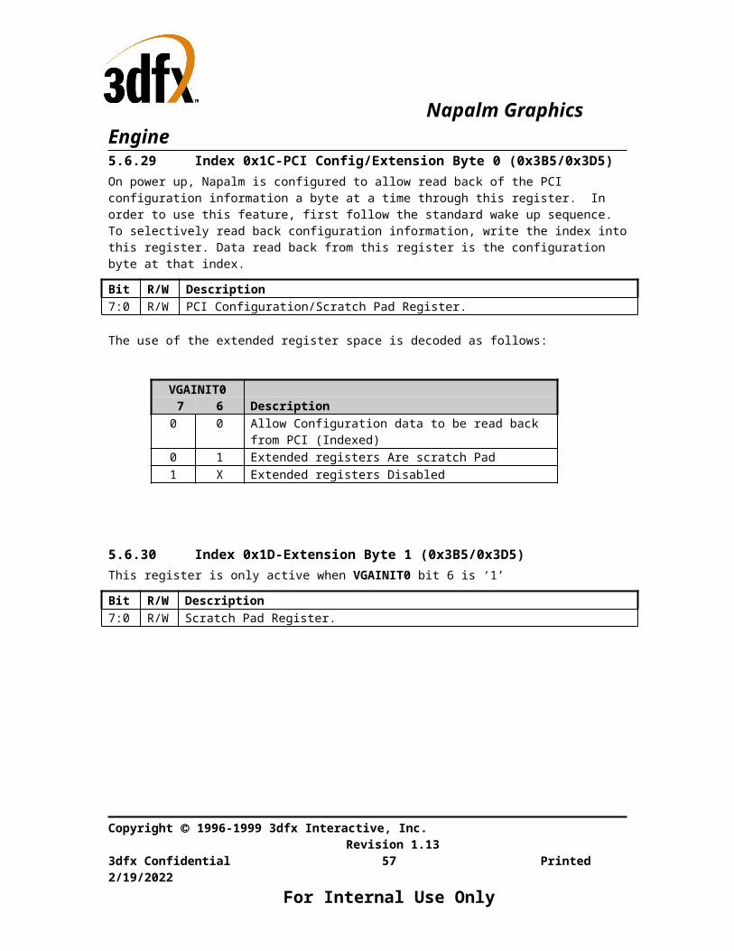
Napalm Graphics Engine 31:24 ROP0
7.2.3 commandExtra RegisterThis register contains miscellaneous control bits in addition to those in the command register.
Bits(1:0) enable colorkeying, if the bit is 0, colorkeying is disabled. Enabling source colorkeying with monochrome source, or in line, polyline, polygon, or rectangle modes has no effect. For further explanation of these bits, see the description of the colorkey registers.
If bit(2) is set, the current command, and any following it will not proceed until the next vertical blanking period begins. Wait for Vsync should not be used when performing non-DMA host blts.
If bit(3) is set, only row 0 of the pattern will be used, rather than the usual 8 pattern rows.
Bit(28) must be set before writing to a 1555 destination surface. IMPORTANT NOTE: You must idle the chip (or write a 3D NOP command) before changing this bit! When this bit is set, the alpha bit of every 1555 pixel is preserved (not overwritten by any 2D operation). Note that this bit should only be set when the destination format (in the dstFormat register) is set to 16bpp. Operating on other destination formats with this bit set will result in unpredicable behavior.
CommandBit Description0 Enable source colorkey (1=source colorkeying enabled, 0=source colorkeying disabled)1 Enable destination colorkey (1=enable dst colorkeying, 0=disable dst colorkeying)2 Wait for Vsync (1=wait for vsync, 0=execute immediately)3 Force pattern row 0 (1 = use only row 0, 0 = use all 8 pattern rows)28:4 Reserved28 Preserve 1-bit alpha31:29 reserved
7.2.4 colorBack and colorFore RegistersThe colorBack and colorFore registers specify the foreground and background colors used in solid-fill and monochrome bitmap operations, and operations using a monochrome pattern. The color registers must be stored in the destination color format.
The following tables shows the format of the color registers for each destination format.
P = palette indexR = red color channelG = green color channelB = blue color channel
Dst Format Bits stored8 bpp 0000_0000_0000_0000_0000_0000_PPPP_PPPP16 bpp 0000_0000_0000_0000_RRRR_RGGG_GGGB_BBBB24 bpp 0000_0000_RRRR_RRRR_GGGG_GGGG_BBBB_BBBB32 bpp AAAA_AAAA_RRRR_RRRR_GGGG_GGGG_BBBB_BBBB
Copyright 1996-1999 3dfx Interactive, Inc. Revision 1.133dfx Confidential 57 Printed 5/7/2023
For Internal Use Only

Napalm Graphics Engine
colorForeBit Description31:0 foreground color
colorBackBit Description31:0 background color
7.2.5 Pattern RegistersThe pattern registers contain an 8 pixel by 8 pixel pattern. The pixels must be either in the color format of the destination surface, or in 1bpp (monochrome) format. The pixels are to be written to the pattern registers in packed format. So, only registers 0 and 1 will be used for monochrome patterns, registers 0 through 15 will be used when the destination is 8 bpp, registers 0 through 31 will be used when the destination is 16 bpp.
Pixels should be written into the pattern registers starting with the upper left-hand corner of the pattern, proceeding horizontally left to right, and then vertically top to bottom. The least-significant bits of pattern[0] should always contain pixel(0,0) of a color pattern.
The table below give the bit position of monochrome pixels within the pattern registers. The bits are numbered such that bit(0) represents the lsb of a register, and bit(31) represents the msb.
7.2.5.1 Order of pixel storage in the pattern registers for a monochrome pattern
pattern(0)Row 0 7 6 5 4 3 2 1 0Row 1 15 14 13 12 11 10 9 8Row 2 23 22 21 20 19 18 17 16Row 3 31 30 29 28 27 26 25 24
pattern(1)Row 4 7 6 5 4 3 2 1 0Row 5 15 14 13 12 11 10 9 8Row 6 23 22 21 20 19 18 17 16Row 7 31 30 29 28 27 26 25 24
pattern(0-64)Bit Description31:0 pattern color data
Copyright 1996-1999 3dfx Interactive, Inc. Revision 1.133dfx Confidential 58 Printed 5/7/2023
For Internal Use Only
Napalm Graphics Engine 7.2.6 srcBaseAddr and dstBaseAddr RegistersBits(25:0) of these registers contain the addresses of the pixels at x=0, y=0 on the source and destination surfaces in frame-buffer memory. Bit(31) of each register specifies whether the address points to tiled or linear memory.
The srcBaseAddr register is used only for screen-to-screen blts. For host-blts, the alignment of the initial pixel sent from the host is determined by the x entry in the srcXY register.
For YUYV422 and UYVY422 surfaces, the base address must be dword aligned. Thus bits(1:0) of srcBaseAddr must be 0.
SrcBaseAddrBit Description25:0 Source base address30:26 RESERVED31 Source memory is tiledBit Description25:0 Destination base address30:26 RESERVED31 Destination memory is tiled
Copyright 1996-1999 3dfx Interactive, Inc. Revision 1.133dfx Confidential 59 Printed 5/7/2023
For Internal Use Only
Napalm Graphics Engine 7.2.7 srcSize and dstSize RegistersThese registers are used only for blts and rectangle fills. They contain the height and width in pixels of the source and destination rectangles. The srcSize register will only be used in Stretch-blt modes. For non-stretched blts, the blt source size will be the same as the blt destination size, determined by the dstSize register.
srcSizeBit Description12:0 Blt Source Width15:13 RESERVED28:16 Blt Source Height31:29 RESERVED
dstSizeBit Description12:0 Blt Destination Width15:13 RESERVED28:16 Blt Destination Height31:29 RESERVED
7.2.8 srcXY and dstXY Registers
During screen-to-screen blts, the srcXY registers sets the position from which blt data will be read. Note that the starting position for a blit depends on the direction of the blt as shown in the table below. For lines and polylines, srcXY is the starting point of the first line segment. For polygons, the srcXY should be the topmost vertex of the polygon - that is, the vertex with the lowest y value. If there are multiple vertices sharing the lowest y value, the srcXY should be set to the leftmost vertex with that y value. Reading the srcXY register while in polygon mode will always return the last polygon vertex that the host sent for the left side of the polygon.
The values in the srcXY are signed, however for blts srcXY must contain only positive values.
During host-to-screen blts, only the x entry of the srcXY register is used. This entry determines the alignment of the initial pixel in the blt within the first dword sent from the host. For monochrome bitmaps, bits[4:0] are used to determine the bit position within the dword of the initial pixel. For color bitmaps, bits[1:0] are give the position within the dword of the first byte of pixel data. Host blts are always performed left-to-right (the x-direction bit in the command register is ignored), so the offset given will always be that of the leftmost pixel in the first span. The alignment of the initial pixel of all spans after the first is determined by adding the source stride (from the srcFormat register) to the alignment of the previous span.
For blts, the dstXY should be the starting pixel of destination rectangle as shown in the table below. For line and polyline modes, the dstXY will be the endpoint of the first line segment.
In polygon mode, the dstXY register is used to store the last vertex sent for the right side of the polygon. If command[8] is set when the command register is written in polygon mode, the value from srcXY will be copied to dstXY. If command[8] is cleared, dstXY can be written with the rightmost pixel in the top span of the polygon.
Command[15:14] Starting X/Y
Copyright 1996-1999 3dfx Interactive, Inc. Revision 1.133dfx Confidential 60 Printed 5/7/2023
For Internal Use Only

Napalm Graphics Engine 00 Upper Left-hand corner01 Upper Right-hand corner10 Lower Left-hand corner11 Lower Right-hand corner
dstXYBit Description12:0 Signed X position on the destination surface15:14 RESERVED28:16 Signed Y position on the destination surface31:30 RESERVED
srcXYBit Description12:0 Signed x position of the first source pixel15:14 RESERVED28:16 Signed y position of the first source pixel31:30 RESERVED
7.2.9 srcFormat and dstFormat RegistersThese register specify the format and strides of the source and destination surfaces
For linear surfaces, the stride of a pixel map is the number of bytes between the starting addresses of adjacent scan lines. For these surfaces, the units of the stride is always bytes, regardless of the pixel format.
For tiled surfaces, the stride is a tile-stride. It’s units are tiles, and only bits(6:0) are used.
The number of bits per pixel is determined as described by the tables below. The ’32 bpp’ format contains 24 bits of RGB, along with a byte of unused data, the ’24 bpp’ is packed 24 bit color.
Data coming through the host port can be byte swizzled to allow conversion between big and little endian formats, as selected by Bit 19 and 20 of src Format register. If both byte and word swizzling are enabled, the byte swizzling occurs first, followed by word swizzling.
The source packing bits control how the stride of the source will be determined during blts. If both bits are zero, the stride is set by the stride entry. Otherwise, the stride is based off of the width of the blt being performed, as shown in the table below. The stride will equal the number of bytes in a row of the rectangle being blted plus as many bytes as are required to get the necessary alignment. Packed source and tiled surfaces are mutually exclusive - you cannot have packed source on a tiled surface.
For YUYV422 and UYVY422 source formats, linear strides must always be a dword multiple. Thus, bits(1:0) of the srcFormat register must be 0.
When necessary, the blt engine will convert source pixels to the destination format.
When source pixels in 16bpp format are converted to 24bpp or 32bpp, color conversion is performed by replicating the msbs of each channel into the extra lsbs required. When pixels are converted from 32bpp
Copyright 1996-1999 3dfx Interactive, Inc. Revision 1.133dfx Confidential 61 Printed 5/7/2023
For Internal Use Only
Napalm Graphics Engine or 24bpp formats to 16bpp, the extra lsbs are removed from each channel. When any non-32bpp format is converted to 32bpp, the 8msbs of each pixel (i.e. the alpha channel) are filled with zeros.
Destination pixel formats are stored as shown in the description of the colorFore and colorBack registers. RGB source formats match these, the other source formats are shown in the table below. For monochrome source, p0 represents the leftmost pixel on the screen and p31 represents the rightmost. For YUV formats, ya represents the left pixel and yb represents the pixel to the right of ya, etc. Thus, ya7 is the msb of the y channel for the left pixel and ya0 is the lsb of the y channel for that pixel. In the diagram, the dword with the lower address (which will be quadword aligned) is shown first, followed by the dword with the higher address.
Source formats
Monochromep24 p25 p26 p27 p28 p29 p30 p31 p16 p17 p18 p19 p20 p21 p22 p23 p8 p9 p10 p11 p12 p13 p14 p15 p0 p1 p2 p3 p4 p5 p6 p7
UYVY 4:2:2yb7 yb6 yb5 yb4 yb3 yb2 yb1 yb0 v7 v6 v5 v4 v3 v2 v1 v0 ya7 ya6 ya5 ya4 ya3 ya2 ya1 ya0 u7 u6 u5 u4 u3 u2 u1 u0
YUYV 4:2:2v7 v6 v5 v4 v3 v2 v1 v0 yb7 yb6 yb5 yb4 yb3 yb2 yb1 yb0 u7 u6 u5 u4 u3 u2 u1 u0 ya7 ya6 ya5 ya4 ya3 ya2 ya1 ya0
Methods of color translation used for Blts1bpp src 8bpp src 16bpp src 24bpp src 32bpp src YUV
src
8bpp dst color registers
direct or palette
not supported not supported
not supported not supported
16bpp dst color registers
not supported
direct lsb removal lsb removal, alpha dropped
YUV => RGB
24bpp dst color registers
not supported
msb duplication
direct direct, alpha dropped
YUV => RGB
32bpp dst color registers
not supported
msb duplication, zero alpha
rgb direct, zero alpha
direct YUV => RGB zero alpha
srcFormatBit Description13:0 Source Stride in bytes or tiles15:14 RESERVED19:16 Source color format: 1, 8, 16, 24, 32 bpp RGB, YUYV422, UYVY42220 Host port byte swizzle (1=enable)21 Host port word swizzle (1=enable)23:22 Source packing31:24 RESERVED
dstFormat
Copyright 1996-1999 3dfx Interactive, Inc. Revision 1.133dfx Confidential 62 Printed 5/7/2023
For Internal Use Only

Napalm Graphics Engine Bit Description13:0 Destination Stride in bytes or tiles15:14 RESERVED18:16 Destination bits per pixel: 8, 16, 24, or 3231:19 RESERVED
srcFormat [19:16]
Source Format dstFormat [18:16]
Destination Bpp
0 1 bpp mono 1 81 8 bpp palettized 3 163 16 bpp RGB 4 244 24 bpp RGB 5 325 32 bpp RGB 8 packed 4:2:2
YUYV9 packed 4:2:2
UYVY
srcFormat[23:22] Packing Stride calculation0 Use stride register srcFormat[13:0]1 Byte packed ceil(src_width * src_bpp/8)2 Word packed ceil(src_width * src_bpp/16)*23 Double-word packed ceil(src_width * src_bpp/32)*4
7.2.10 clip0Min, clip0Max, clip1Min, and clip1Max RegistersThe clip registers define the maximum and minimum x & y values of pixel that can be written in the destination pixel map. There are two sets of clip registers, however, only one set is used at a time, as determined by the clip select bit in the command register.
Clipping is inclusive of the minimum values, and exclusive of the maximum values. Thus if the clip select bit is zero, only pixels with x values in the range [clip0Min_x, clip0Max_x) and y values in the range [clip0Min_y, clip0Max_y) will be written.
clip0MinBit Description11:0 x minimum clip when clip select is 015:12 RESERVED27:16 y minimum clip when clip select is 031:28 RESERVED
clip0MaxBit Description11:0 x maximum clip when clip select is 015:12 RESERVED27:16 y maximum clip when clip select is 0
Copyright 1996-1999 3dfx Interactive, Inc. Revision 1.133dfx Confidential 63 Printed 5/7/2023
For Internal Use Only
Napalm Graphics Engine 31:28 RESERVED
clip1MinBit Description11:0 x minimum clip when clip select is 115:12 RESERVED27:16 y minimum clip when clip select is 131:28 RESERVED
clip1MaxBit Description11:0 x maximum clip when clip select is 115:12 RESERVED27:16 y maximum clip when clip select is 131:28 RESERVED
7.2.11 colorkey RegistersThese registers define the range of colors that will be transparent when color keying is enabled.
Different ROPs are selected for each pixel depending the result of that pixels colorkey test. A source pixel passes the colorkey test if it is within the inclusive range defined by the srcColorkeyMin and srcColorkeyMax registers. A destination pixel passes the colorkey test if it is within the inclusive range defined by the dstColorkeyMin and dstColorkeyMax registers.
For Pixels with 8bpp formats, the color indices are compared directly. For pixels with 16, 24, or 32bpp formats, each color channel (R, G, and B) is compared separately, and each channel must pass for the colorkey test to be passed. In the 32bpp format, the upper 8 bits are ignored during colorkey testing. Source colorkeying cannot be enabled if the source format is 1 bpp.
If colorkeying is disabled for the source or destination surfaces, that colorkey test is failed.
For further information on ROP selection by the colorkey test results, see the description of the ROP register.
The colorkey test uses the following formula:pass = (((color>=colorkey_min) && (color<=colorkey_max)) && colorkey_enable)
srcColorkeyMinBit Description23:0 minimum color key value for source pixels31:24 RESERVED
srcColorkeyMaxBit Description23:0 maximum color key value for source pixels31:24 RESERVED
dstColorkeyMin
Copyright 1996-1999 3dfx Interactive, Inc. Revision 1.133dfx Confidential 64 Printed 5/7/2023
For Internal Use Only
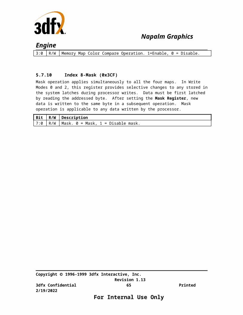
Napalm Graphics Engine Bit Description23:0 minimum color key value for destination pixels31:24 RESERVED
dstColorkeyMaxBit Description23:0 maximum color key value for destination pixels31:24 RESERVED
7.2.12 rop RegisterThis is a set of ternary ROPs used to determine how the source, destination, and pattern pixels will be combined. The default ROP, ROP0 is stored in the command register. Which of the four ROPs will be used is determined on a per-pixel basis, based on the results of the source and destination colorkey tests, as shown in the following table:
Source Color Key Test
Destination Color Key Test
ROP
Fail Fail ROP 0Fail Pass ROP 1Pass Fail ROP 2Pass Pass ROP 3
ropBit Description7:0 ROP 115:8 ROP 223:16 ROP 3
7.2.13 lineStyle registerThe lineStyle register specifies how lines will be drawn.
The bit pattern used for line stippling can be set to repeat every 1-32 bits, as set by the bit-mask size part of this register. The bit-mask size entry gives the number of bits *minus one* that will be used from the lineStipple register. Thus, if you want to use 2 bits to represent a dashed line, you would set the bit-mask size to 1.
Each bit from the lineStipple register will determine the color or transparency of from 1-256 pixels. The repeat count determines the number of pixels along the line that will be drawn (or skipped) for each bit in the line pattern register. The number of pixels associated with each bit of the line pattern *minus one* must be written to the repeat count entry.
The start position give the offset within the line pattern register for the first pixel drawn in a line. It consists of an integer index of the current bit in the line pattern, and a fractional offset that will determine the number of pixels that will be drawn using that bit of the pattern. The number of pixels drawn using the initial bit in the line pattern will equal the repeat count (i.e. the repeat count entry+1) minus the
Copyright 1996-1999 3dfx Interactive, Inc. Revision 1.133dfx Confidential 65 Printed 5/7/2023
For Internal Use Only
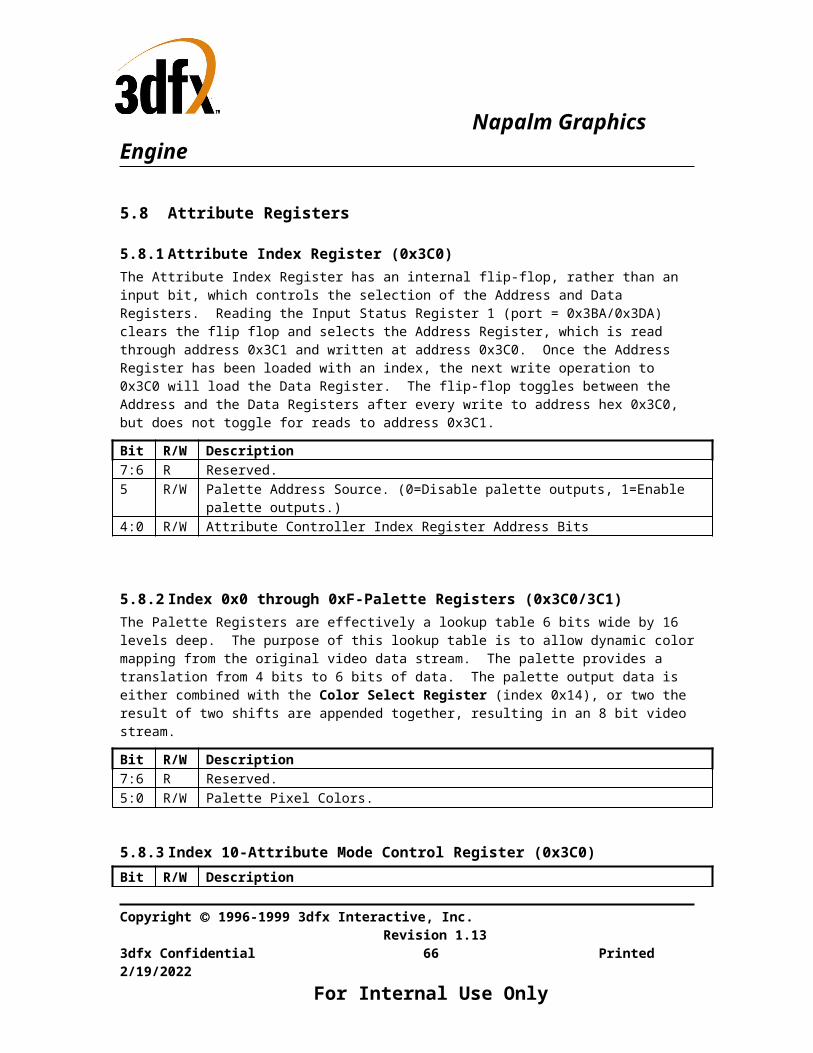
Napalm Graphics Engine fractional part of the start position. The bit positions within the lineStipple registers are numbered starting with the lsb at 0, going up to the msb at 31.
It is illegal to set the integer part of the stipple position to be greater than the bit-mask size. It is illegal to set the fractional part to be greater than the repeat count. If either part of the stipple position is too large, the behavior of the line drawing engine is undefined.
Writing the lineStyle register will cause the stipple position to be loaded from the register. If the lineStyle register is not written to between the execution of two line commands, the stipple position at the start of the new line will be whatever if was after the completion of the last line. If the lineStyle register is read while the 2D engine is idle, the stipple position read will always be that which will be used in the next line operation - thus, if the lineStyle register has been written since the last stippled line was drawn the value written will be returned, otherwise the value that remained after the last stippled line will returned. Reading the lineStyle register while the 2D engine is not idle will return an indeterminable value for the stipple position.
In the following examples,. ‘x’ represents a pixel colored with colorFore, ‘o’ represents a pixel colored with colorBack or that is transparent. ‘_S_’ Shows that the line engine is starting at bit 0 in the lineStipple register. ‘_’ shows that the line engine is using a new bit from the lineStipple register.
7.2.13.1 ExampleSay the bit-mask size is set to 6 (thus, the entry in the register is 5) and the line pattern is:lineStipple <= 010111b
The pixel pattern that will be repeated is:
repeat_count repeating pixel pattern1 x_x_x_o_x_o_S_x_x_x_o_x_o2 xx_xx_xx_oo_xx_oo_S_xx_xx_xx_oo_xx_oo3 xxx_xxx_xxx_ooo_xxx_ooo_S_xxx_xxx_xxx_ooo_xxx_ooo
7.2.13.2 ExampleSay the repeat count is 5 (the register entry is 4), the integer part of the start position is 7, and the fractional part of the start position is 2. The color of the first 3 pixels drawn for the line will be determined by bit 7 in the line pattern register, the next 5 pixels will be determined by bit 8, and so on.
lineStyle <= 07020904hlineStipple <= 1010110111b
pixels generated, where x=colorFore and o=colorBack:
xxx_ooooo_xxxxx_S_xxxxx_xxxxx_xxxxx_ooooo_xxxxx_xxxxx_ooooo_xxxxx_ooooo_xxxxx_S
7.2.13.3 Pseudo code for line pixel generationHere is the pseudo-code for determining the color of pixels generated by the line engine:
<bit_position> = <start_position_integer>
Copyright 1996-1999 3dfx Interactive, Inc. Revision 1.133dfx Confidential 66 Printed 5/7/2023
For Internal Use Only

Napalm Graphics Engine <pixel_position> = <start_position_fraction>
while (<need_another_pixel>) { if ( <line_pattern> & (1 << <bit_position>) ) {
<new_pixel_color> = <colorFore> } else {
if (<transparent>) { <new_pixel_color> = <transparent>} else { <new_pixel_color> = <colorBack>}
}
if ( <pixel_position> == <repeat_count> ) {<pixel_position> = 0if (<bit_position> == <bit_mask_size>) {
<bit_position> = 0;} else {
<bit_position> = <bit_position> + 1}
} else {<pixel_position> = <pixel_position> +1
}
}
lineStyleBit Description7:0 Repeat count12:8 Stipple size15:13 RESERVED23:16 Start position - fractional part28:24 Start position - integer part31:29 RESERVED
7.2.14 lineStipple RegisterThe line bit-mask register contains a mask that determines how lines will be drawn. Bits that are ones will be drawn with the color in the colorFore register. Bits that are zeros will be filled with the color in the colorBack register, or will not be filled, depending on the ‘transparent’ bit in the command register. The pattern in the bit mask can be set to repeat every 1-32 bits, as set by the bit-mask size part of the line style register. If the bit-mask size is set to less than 31, some of the bits of the line bit-mask will not be used, starting with the most-significant bit. For example, if the bit-mask size is set to 7, bits 0-7 of the lineStipple register will contain the line bit-mask.
lineStippleBit Description31:0 Line bit-mask
Copyright 1996-1999 3dfx Interactive, Inc. Revision 1.133dfx Confidential 67 Printed 5/7/2023
For Internal Use Only
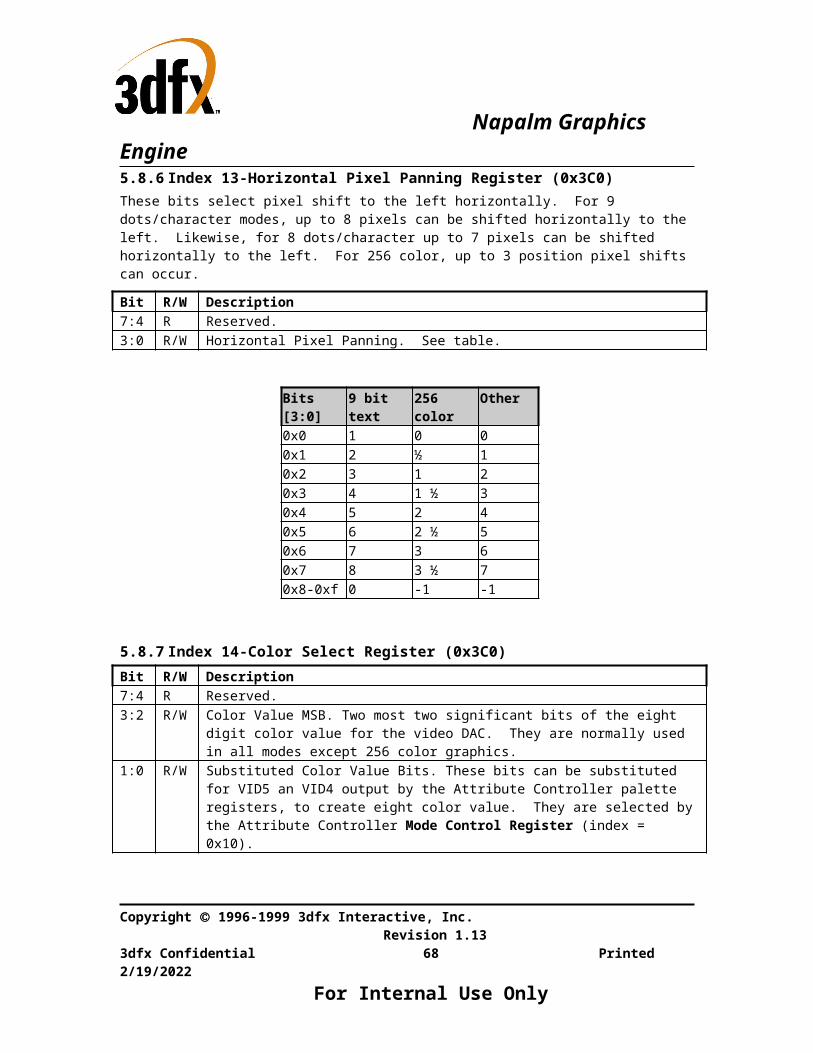
Napalm Graphics Engine 7.2.15 bresenhamError registersThese registers allows the user to specify the initial Bresenham error terms used when performing line drawing, polygon drawing, and stretch blts. The Bresenham error terms are signed values.
Bit 31 of each registers determines whether or not the error term given in the lower bits will be used. If this bit is 0, the line and stretch blt engines will generate the initial error term automatically. If the bit is set to 1, the error term given in bits 16-0 will be used. If a bresenham error register is used, the register should be written with bit[31] set to 0 after completion of the operation, so that subsequent operations will not be affected.
bresError0 can be used to set the initial error value for lines, for the left edge of a polygon, and for blt stretching along the y-axis.
bresError1 can be used to set the initial error value for the right edge of a polygon, and for blt stretching along the x-axis.
bresError0Bit Description15:0 Signed Bresenham error term for stretch blt y, lines, and left polygon edges 30:17 RESERVED31 Use the error term given in bits 16-0
bresError1Bit Description15:0 Signed Bresenham error term for stretch blt x and right polygon edges30:17 RESERVED31 Use the error term given in bits 16-0
7.3 Launch Area
7.3.1 Screen-to-screen Blt ModeWriting the launch area while in screen-to-screen blt mode results in a rectangle being copied from one area of display memory to another. The position of the source rectangle is given by the write to the launch area. The write to the launch area will be used to fill the srcXY register.
screenBltLaunchBit Description12:0 X position of the source rectangle15:13 RESERVED28:16 Y position of the source rectangle31:29 RESERVED
7.3.2 Screen-to-screen Stretch Blt ModeWriting the launch area while in screen-to-screen blt mode results in pixels being copied from rectangle in display memory to another of a different size. The write to the launch area will be used to fill the srcXY register. The x and y direction bits do not apply to stretch blits. I.e., only top-down, left-to-right stretch blits can be done.Copyright 1996-1999 3dfx Interactive, Inc. Revision 1.133dfx Confidential 68 Printed 5/7/2023
For Internal Use Only

Napalm Graphics Engine
stretchBltLaunchBit Description12:0 X position of the source rectangle15:13 RESERVED28:16 Y position of the source rectangle31:29 RESERVED
7.3.3 Host-to-screen Blt ModeIn host-to-screen blt mode, writes to the launch area should contain packed pixels to be used as source data. When performing a host-to-screen blt, the blt engine does not generate source addresses. However, it is still necessary for the driver to specify the srcFormat, in order for the blt engine to determine how the source data is packed. The driver must also write the srcXY register in order to specify the first byte or bit to use from the first dword. In monochrome source mode, the 5 lsbs will specify the initial bit. In all other modes, the 2 lsbs of srcXY will specify the initial byte of the initial span. The alignment of the first pixel of each span after the first is determined by adding the source stride (from the srcFormat register) to the alignment of the previous span.
If more data is written to the launch area than is required for the host blt specified, the extra data will be discarded, or may be used in the following host blt, if it is requested while the 2D is operating on the firsthblt. If too little data is written to the launch area, the hblt will be aborted, and pixels on an incomplete span at the end of the host blt may or may not be drawn.
7.3.3.1 Host Blt Example 1In this example, the driver is drawing text to a 1024x768x16bpp screen using monochrome bitmaps of various widths. The monochrome data is packed, with each row byte aligned. First, it sets up the necessary registers before giving the data specific to the first blt:
colorBack <= the background color
colorFore <= the foreground color
dstXY <= the starting position of the first character
dstBaseAddr <= base address of the primary surface
clip0Min <= 0x00000000
clip0Max <= 0xFFFFFFFF
command <= SRC_COPY || HOST_BLT_MODE = 0xCC000003
dstFormat <= 0x00030800
srcFormat <= 0x00400000
The command mode is set to host-to-screen blt, with all other features disabled. Since colorkeying is disabled, only ROP0 is needed. The format register sets the host format to unswizzled monochrome, using byte-packing. This means that the stride will not have to be set for each blt, but will be set to the number of bytes required to store the number of pixels in the source width (Since this is not a stretch blt, the source width equals the destination width, as set later in the dstSize register). The clip registers are set such that the results will not be clipped. Although this is a host to screen blt, the srcXY register must Copyright 1996-1999 3dfx Interactive, Inc. Revision 1.133dfx Confidential 69 Printed 5/7/2023
For Internal Use Only

Napalm Graphics Engine be set in order to specify the initial alignment of the bitmask. For this example, the source data begins with the lsb of the first dword of host data, so the srcXY register is set to zero.
Now, the driver is ready to start the first blt. It will blt a 11x7 pixel character.
dstSize <= 0x0007000B
srcXY <= 0x00000000
launch <= 0xc0608020
launch <= 0xC460C060
launch <= 0x3B806EC0
launch <= 0x00001100
7.3.3.2 Host Blt Example 2In this example, the driver is drawing a pixel map
colorBack <= the background color
colorFore <= the foreground color
dstXY <= the starting position of the first character
clip0Min <= 0x00000000
clip0Max <= 0xFFFFFFFF
command <= SRC_COPY || HOST_BLT_MODE = 0xCC000003
srcFormat <= 0x00240000
The command mode is set to host-to-screen blt, with all other features disabled. Since colorkeying is disabled, only ROP0 is needed. The format register sets the host format to unswizzled monochrome, using byte-packing. This means that the stride will not have to be set for each blt, but will be set to the number of bytes required to store the number of pixels in the source width (Since this is not a stretch blt, the source width equals the destination width, as set later in the dstSize register). The clip registers are set such that the results will not be clipped. Although this is a host to screen blt, the srcXY register must be set in order to specify the initial alignment of the bitmask. For this example, the source data begins with the lsb of the first dword of host data, so the srcXY register is set to zero.
Now, the driver is ready to start the first blt. It will blt a 11x7 pixel character.
dstXY <= 0x0007000B
srcXY <= 0x00000000
launch <= 1st 2 rows
launch <= 2nd 2 rows
launch <= 3rd 2 rows
launch <= last row
hostBltLaunch
Copyright 1996-1999 3dfx Interactive, Inc. Revision 1.133dfx Confidential 70 Printed 5/7/2023
For Internal Use Only

Napalm Graphics Engine Bit Description31:0 Source pixel data
7.3.4 Host-to-screen Stretch Blt ModeWriting the launch area while in host-to-screen blt mode results in the pixels written to the launch area being stretched onto the destination rectangle. Pixel data for Host-to-screen stretch blts is written just as for non-stretched host-to-screen blts, except when the destination height differs from the source height. In this case, the host must replicate or decimate the source spans to match the number of destinations spans required.
hostStretchLaunchBit Description31:0 Source pixel data
7.3.5 Rectangle Fill ModeRectangle fill mode is similar to screen-to-screen blt mode, but in this mode, the colorFore register is used as source data rather than data from display memory. The size of the rectangle is determined by the dstSize register. The write to the launch area gives the position of the destination rectangle, which is used to fill the dstXY register.
rectFillLaunchBit Description12:0 X position of the destination rectangle15:13 RESERVED28:16 Y position of the destination rectangle31:29 RESERVED
7.3.6 Line ModeWriting the launch area while in line mode will write the launch data to the dstXY register and draw a line from srcXY to dstXY. After the line has been drawn, dstXY is copied to srcXY. In line mode, all pixels in the line will be drawn (as specified by the line style register), including both the start and endpoint.
The ROP used for lines can use the pattern and the destination, but not source data. colorFore will be used in the ROP in place of source data. Source colorkeying must be turned off, destination colorkeying is allowed.
7.3.6.1 Line drawing example
srcXY <= 0x00020003 // line start-point = (3, 2)
lineStipple <= 0x00000006 // bit mask is 110 binary
lineStyle <= 0x02010202 // start position = 2 1/3, repeat count = 2, bit-mask size=2
Copyright 1996-1999 3dfx Interactive, Inc. Revision 1.133dfx Confidential 71 Printed 5/7/2023
For Internal Use Only
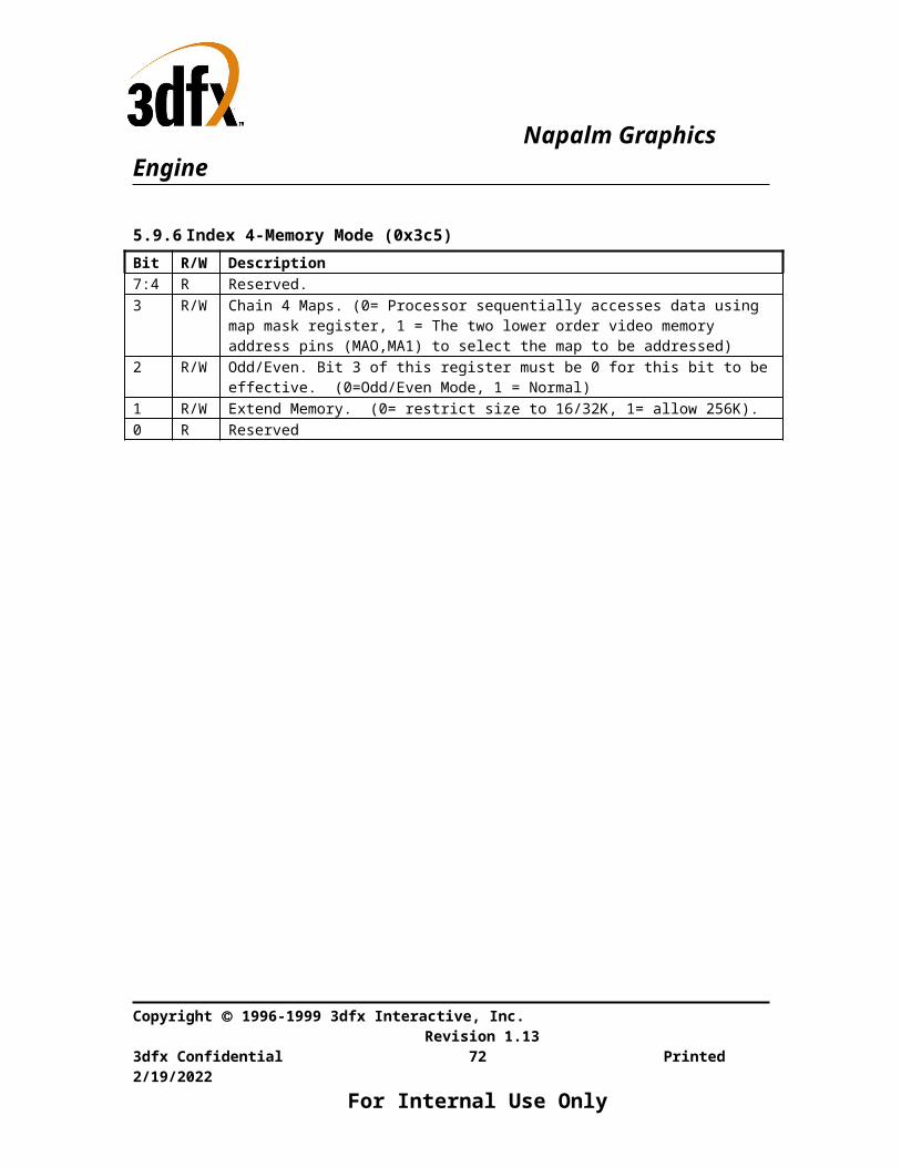
Napalm Graphics Engine
colorBack <= BLACK
colorFore <= GREY
command <= LINE_MODE || OPAQUE
launch <= 0x000c0016 // line end-point = (22,12)
The line drawn will appear as shown below:
Origin
Figure 1
lineLaunchBit Description12:0 X position of the line endpoint15:13 RESERVED28:16 Y position of the line endpoint31:29 RESERVED
7.3.7 Polyline ModeWriting the launch area while in line mode will write the launch data to the dstXY register and draw a line from srcXY to dstXY. After the line has been drawn, dstXY is copied to srcXY. In polyline mode, the endpoint of the line (the pixel at dstXY) will not be written. This ensures that each pixel in a non-overlapping polyline will be written only once.
The ROP used for lines can use the pattern and the destination, but not source data. colorFore will be used in the ROP in place of source data. Source colorkeying must be turned off, destination colorkeying is allowed.
polylineLaunchBit Description12:0 X position of the line endpoint15:13 RESERVED28:16 Y position of the line endpoint
Copyright 1996-1999 3dfx Interactive, Inc. Revision 1.133dfx Confidential 72 Printed 5/7/2023
For Internal Use Only
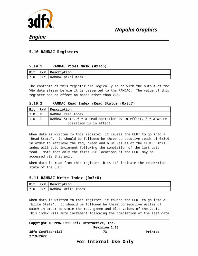
Napalm Graphics Engine 31:29 RESERVED
7.3.8 Polygon Fill ModeThe polygon fill mode can be used to draw simple polygons. A polygon may be drawn using the method described below if no horizontal span intersects more than two non-horizontal polygon edges. Polygons are drawn by first determining the top vertex - that is the vertex with the lowest y coordinate. The coordinates of this vertex should be written to the srcXY register. If multiple vertices share the lowest y coordinate, any vertex with the lowest y coordinate may be used as the starting point. If command[8] is set when the command register is written when command[3:0] indicates polygon mode, the value in the srcXY register will be copied to the dstXY register. The value in the srcXY register determines the starting point for the left side of the polygon, while the value in the dstXY register determines the starting point for the right side of the polygon. If bit[8] of the command register is not set, the starting position of the right side of the polygon can be set by writing to the dstXY register.
Once the starting vertex is set, as well as the desired colors, ROP, pattern, and options for the polygon fill, the polygon can be drawn by writing polygon vertices to the launch area. When multiple vertices share the lowest y coordinate, the starting vertex chosen will determine which of those vertices are on the ‘right’ edge of the polygon and which are on the ‘left’ edge. Pixels with the same y value as the starting point are on the left edge if they are to the left of the starting point.
For optimum performance, software should determine the leftmost and rightmost of all vertices that share the lowest y coordinate. The coordinates of the leftmost vertex should be written to srcXY and the coordinates of the rightmost vertex should be written to dstXY. When the command register is written, command[8] (the ‘start command’ bit) should be low.
In Polygon fill mode, polygon vertices should be written to the launch area in order of increasing y value. Whenever 2 vertices share the same y value, the leftmost vertex *must* be written first. The driver should keep track of the last y value sent for the left and right sides. If the y value for the last vertex sent for the left side is *less than or equal to* the last y value sent for the right side, the next vertex on the left side should be written to the launch area. Otherwise, the next vertex for the right side should be written to the launch area.
The ROP used for filling polygons can use the pattern and the destination, but not source data. colorFore will be used in the ROP in place of source data. Source colorkeying must be turned off, destination colorkeying is allowed.
Pixels that are on the line that forms the left edge of the polygon will be drawn. Pixels that fall on the line that forms the right edge of the polygon will not be drawn. For Horizontal edges, pixels on a horizontal polygon edge that is on the ‘top’ of the polygon (i.e. above the edge is outside the polygon and below the edge is inside the polygon) will be drawn, while pixels on a horizontal polygon edge that is on the bottom of the polygon will not be drawn.
7.3.8.1 Polygon drawing exampleAs an example of polygon drawing, say we are drawing the polygon shown in figure 2. Traversing the vertex list in counterclockwise order gives the following list of vertices:
(4, 1) (2, 4) (3, 6) (1, 6) (2,8) (5, 11) (8,8) (13,8) (11,6) (11,3) (10,1)
Figures 2a through 2m show the steps in drawing the polygon. Filled circles are vertices of the left polygon edge. Open circles are vertices of the right polygon edge. Pixels that are drawn at the end of each step are shaded in the figures.
Copyright 1996-1999 3dfx Interactive, Inc. Revision 1.133dfx Confidential 73 Printed 5/7/2023
For Internal Use Only

Napalm Graphics Engine The polygon engine keeps track of four vertices at a time. The top vertex of the current left polygon edge (L0), the bottom vertex of the current left polygon edge (L1), the top vertex of the current right polygon edge (R0), and the bottom vertex of the current right polygon edge (R1). The values of these variables at each step in drawing the polygon are shown in the figures. The arrows in the figures indicate when a variable changes between the start of the step and the end of pixel filling for that step.
Figure 2
First, all required registers must be written, including the dstFormat register to specify the drawing surface, color or pattern registers, and the command register. Write the coordinates of the starting vertex (4, 1) to the srcXY register:
srcXY <= 0x00010004
command <= POLYGON_MODE || INITIATE_COMMAND
Copyright 1996-1999 3dfx Interactive, Inc. Revision 1.133dfx Confidential 74 Printed 5/7/2023
For Internal Use Only
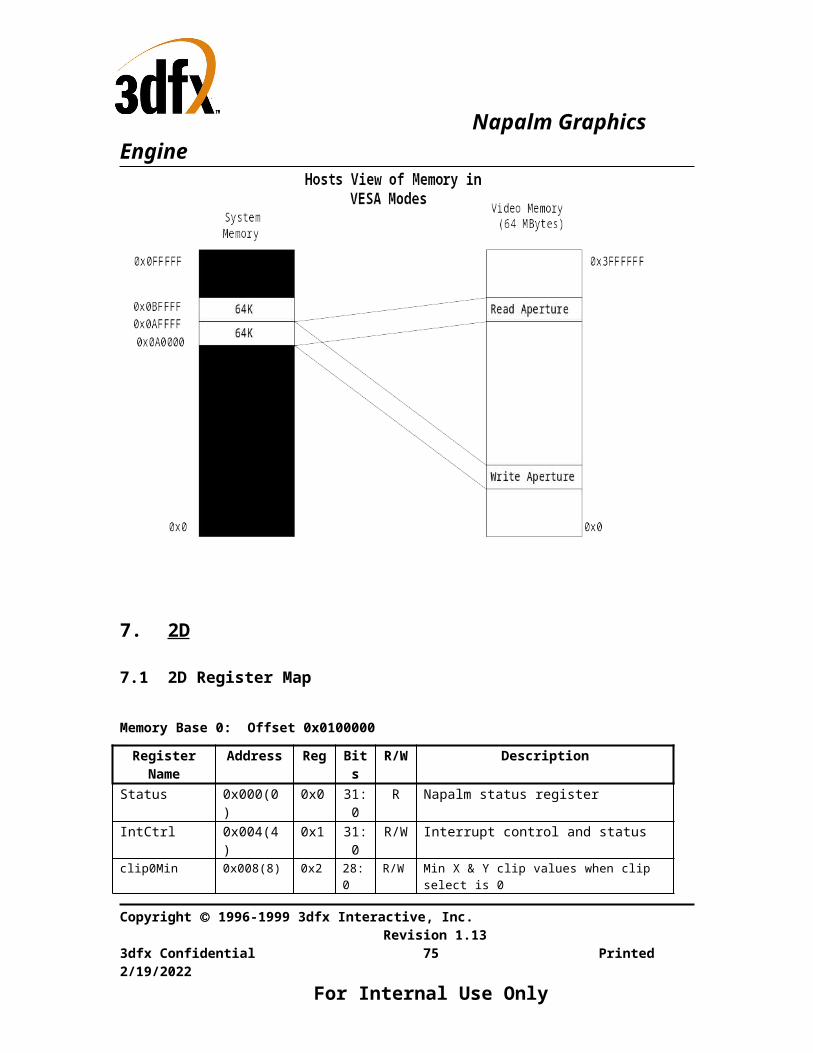
Napalm Graphics Engine
L0L1 R1
R0
Figure 2a
R1.y>=L1.y, so we have to write the next vertex for the left edge (2, 4):
launch <= 0x00040002
L0
L1
R1R0
Figure 2b
R1.y<L1.y, so we write the next vertex for the right edge (10, 2). The drawing engine now has edges for both the left and right edges. So, it will draw all spans up to min(R1.y, L1.y). Because R1.y=R0.y, no pixels will be drawn, but R0 will be updated to vertex R1:
launch <= 0x0001000a
R0L0
L1
R1R0
Figure 2c
Copyright 1996-1999 3dfx Interactive, Inc. Revision 1.133dfx Confidential 75 Printed 5/7/2023
For Internal Use Only

Napalm Graphics Engine
R1.y<L1.y, so we again write the next vertex on the right polygon edge (11, 3). Pixels on all spans from max(L0.y, R0.y) to min(L1.y, R1.y)-1 will be drawn, as shown below. Because R1.y<L1.y, R0 is updated to R1.
launch <= 0x0003000b
R0
L0
L1R1
R0
Figure 2d
R1.y<L1.y, so we write the next vertex on the right edge (11, 6). Again, pixels on all spans from max(L0.y, R0.y) to min(L1.y, R1.y)-1 will be drawn. This time R1.y>L1.y, however, so L0 is updated to L1.
launch <= 0x0006000b
R0
L0
L1L0
R1
Figure 2e
R1.y>=L1.y, so we write the next vertex on the left edge (3, 6). L1.y=R1.y, so R0 is updated to R1 and L0 is updated to L1.
Copyright 1996-1999 3dfx Interactive, Inc. Revision 1.133dfx Confidential 76 Printed 5/7/2023
For Internal Use Only

Napalm Graphics Engine
launch <= 0x00060003
R0L0
R1R0L0
L1
Figure 2f
R1.y>=L1.y, so we write the next vertex on the left edge (1, 6). L1.y=R1.y, so R0 is updated to R1 and L0 is updated to L1. R1 did not change, so updating R0 to R1 has no effect.
launch <= 0x00060001
R1R0L0
L1L0
Figure 2g
R1.y>=L1.y, so we again write the next vertex on the left edge (2, 8). L1.y>R1.y, so R0 is updated to R1, again with no effect.
launch <= 0x00080002
Copyright 1996-1999 3dfx Interactive, Inc. Revision 1.133dfx Confidential 77 Printed 5/7/2023
For Internal Use Only
Napalm Graphics Engine
R1R0
L1
L0
Figure 2h
R1.y<L1.y, so we write the next vertex on the right edge (11, 8). L1.y=R1.y, so R0 is updated to R1, and L0 is updated to L1.
launch <= 0x0008000b
R1
R0
L1
L0
L0 R0
Copyright 1996-1999 3dfx Interactive, Inc. Revision 1.133dfx Confidential 78 Printed 5/7/2023
For Internal Use Only
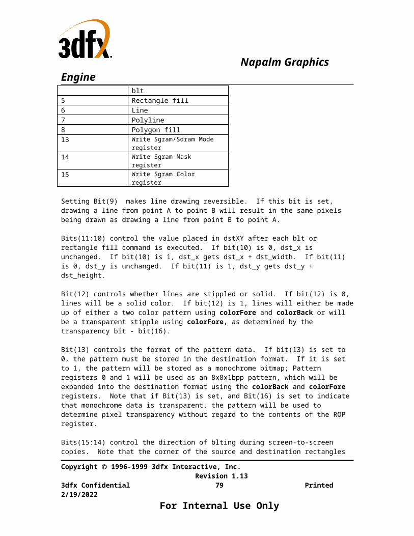
Napalm Graphics Engine
Figure 2i
R1.y>=L1.y, so we write the next vertex on the left edge (5, 11). L1.y>R1.y, so R0 is updated to R1.
launch <= 0x000b0005
R1L0
L1
R0
Figure 2j
R1.y<L1.y, so we write the next vertex on the right edge (8, 8). L1.y>R1.y, so R0 is updated to R1, but no pixels are drawn.
launch <= 0x00080008
Copyright 1996-1999 3dfx Interactive, Inc. Revision 1.133dfx Confidential 79 Printed 5/7/2023
For Internal Use Only

Napalm Graphics Engine
R1L0
L1
R0 R0
Figure 2k
R1.y<L1.y, so we write the next vertex on the right edge. This is the final vertex in the polygon, which doesn’t have a horizontal span at the bottom, so this vertex is the same as the last vertex for the left edge (5, 11). L1.y=R1.y, so R0 is updated to R1, and L0 is updated to L1. No pixels on the final span are drawn (this would be true even if L1.x did not equal R1.x). If the launch area is written again before any registers are written the polygon engine will begin a new polygon starting at (5,11).
launch <= 0x000b0005
Copyright 1996-1999 3dfx Interactive, Inc. Revision 1.133dfx Confidential 80 Printed 5/7/2023
For Internal Use Only

Napalm Graphics Engine
R1
L0
L1
R0
R0L0
Figure 2m
polygonLaunchBit Description12:0 X position of a polygon vertex15:13 RESERVED28:16 Y position of a polygon vertex31:29 RESERVED
7.4 Miscellaneous 2D
7.4.1 Write Sgram/Sdram Mode RegisterExecuting this command causes the value in colorFore[13:0] to be set as the sgram/sdram mode register via a special bus cycle in the memory controller.
SGRAM mode registerBit Description2:0 burst length3 burst type (0=sequential, 1=interleave)6:4 CAS latency8:7 test mode9 write burst length (0=burst, 1=single bit).
Copyright 1996-1999 3dfx Interactive, Inc. Revision 1.133dfx Confidential 81 Printed 5/7/2023
For Internal Use Only

Napalm Graphics Engine 10 sgram-defined.
The colorFore register is mapped to the Sgram/Sdram pins as follows:
ColorFore registerBit Description11:0 Address pins fb_addr[11:0]12 Address bank select fb_ba[1] (equivalent to fb_addr[12] in some memory
configurations)13 Address bank select fb_ba[0]
7.4.2 Write Sgram Color RegisterExecuting this command causes the value in colorFore[31:0] to be set as the sgram color register via a special bus cycle in the memory controller. Since Napalm has a 128-bit wide bus, the register is replicated across the four sets of sgram memories.
7.4.3 Write Sgram Mask RegisterExecuting this command causes the value in colorFore [31:0] to be set as the sgram mask register via a special bus cycle in the memory controller. Since Napalm has a 128-bit wide bus, the register is replicated across the four sets of sgram memories.
8. 3D Memory Mapped Register Set A 4Mbyte (22-bit) FBI memory mapped register address is divided into the following fields:
AltMap Swizzle Wrap Chip Register Byte1 1 6 4 8 2
The chip field selects one or more of the Napalm units (FBI and/or TREX) to be accessed. Each bit in the chip field selects one chip for writing, with FBI controlled by the lsb of the chip field, and TREX#2 controlled by the msb of the chip field. Note the chip field value of 0x0 selects all chips. The following table shows the chip field mappings:
Chip Field Napalm Unit Accessed0000 FBI + all TREX chips0001 FBI0010 TREX #00011 FBI + TREX #00100 TREX #10101 FBI + TREX #1
Copyright 1996-1999 3dfx Interactive, Inc. Revision 1.133dfx Confidential 82 Printed 5/7/2023
For Internal Use Only
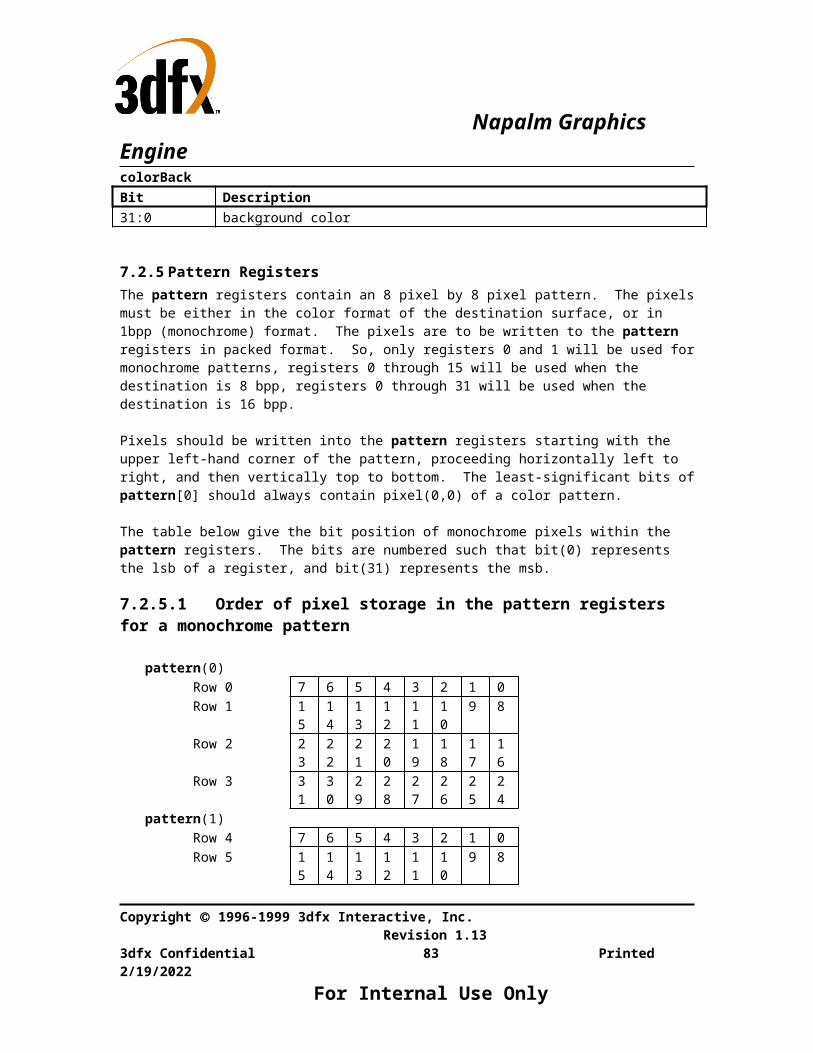
Napalm Graphics Engine
0110 TREX #0 + TREX #10111 FBI + TREX #0 + TREX #11000 TREX #21001 FBI + TREX #21010 TREX #0 + TREX #21011 FBI + TREX #0 + TREX #21100 TREX #1 + TREX #21101 FBI + TREX #1 + TREX #21110 TREX #0 + TREX #1 + TREX
#21111 FBI + all TREX chips
By utilizing the different chip fields, software can precisely control the data presented to individual chips which compose the Napalm graphics subsystem. Note that for reads, the chip field is ignored, and read data is always read from FBI. The register field selects the register to be accessed from the table below. All accesses to the memory mapped registers must be 32-bit accesses. No byte (8-bit) or halfword (16-bit) accesses are allowed to the memory mapped registers, so the byte (2-bit) field of all memory mapped register accesses must be 0x0. As a result, to modify individual bits of a 32-bit register, the entire 32-bit word must be written with valid bits in all positions.
The table below shows the Napalm register set. The register set shown below is the address map when triangle registers address aliasing (remapping) is disabled(fbiinit3(0)=0). When The chip column illustrates which registers are stored in which chips. For the registers which are stored in TREX, the % symbol specifies that the register is unconditionally written to TREX regardless of the chip address. Similarly, the * symbol specifies that the register is only written to a given TREX if specified in the chip address. The R/W column illustrates the read/write status of individual registers. Reading from a register which is “write only” returns undefined data. Also, reading from a register that is TREX specific returns undefined data.. Reads from all other memory mapped registers only contain valid data in the bits stored by the registers, and undefined/reserved bits in a given register must be masked by software. The sync column indicates whether the graphics processor must wait for the current command to finish before loading a particular register from the FIFO. A “yes” in the sync column means the graphics processor will flush the data pipeline before loading the register -- this will result in a small performance degradation when compared to those registers which do not need synchronization. The FIFO column indicates whether a write to a particular register will be pushed into the PCI bus FIFO. Care must be taken when writing to those registers not pushed into the FIFO in order to prevent race conditions between FIFOed and non-FIFOed registers. Also note that reads are not pushed into the PCI bus FIFO, and reading FIFOed registers will return the current value of the register, irrespective of pending writes to the register present in the FIFO.
Memory Base 0: Offset 0x0200000Register Name Address Reg
NumBits Chip R/
WSync? /Fifo?
Description
status 0x000(0) 0x0 31:0 FBI R No / n/a Napalm StatusintrCtrl 0x004(4) 0x1 31:0 FBI R/W No / No Interrupt Status and ControlvertexAx 0x008(8) 0x2 15:0 FBI+TREX% W No / Yes Vertex A x-coordinate location (12.4 format)vertexAy 0x00c(12) 0x3 15:0 FBI+TREX% W No / Yes Vertex A y-coordinate location (12.4 format)vertexBx 0x010(16) 0x4 15:0 FBI+TREX% W No / Yes Vertex B x-coordinate location (12.4 format)vertexBy 0x014(20) 0x5 15:0 FBI+TREX% W No / Yes Vertex B y-coordinate location (12.4 format)vertexCx 0x018(24) 0x6 15:0 FBI+TREX% W No / Yes Vertex C x-coordinate location (12.4 format)vertexCy 0x01c(28) 0x7 15:0 FBI+TREX% W No / Yes Vertex C y-coordinate location (12.4 format)
startR 0x020(32) 0x8 23:0 FBI W No / Yes Starting Red parameter (12.12 format)startG 0x024(36) 0x9 23:0 FBI W No / Yes Starting Green parameter (12.12 format)
Copyright 1996-1999 3dfx Interactive, Inc. Revision 1.133dfx Confidential 83 Printed 5/7/2023
For Internal Use Only
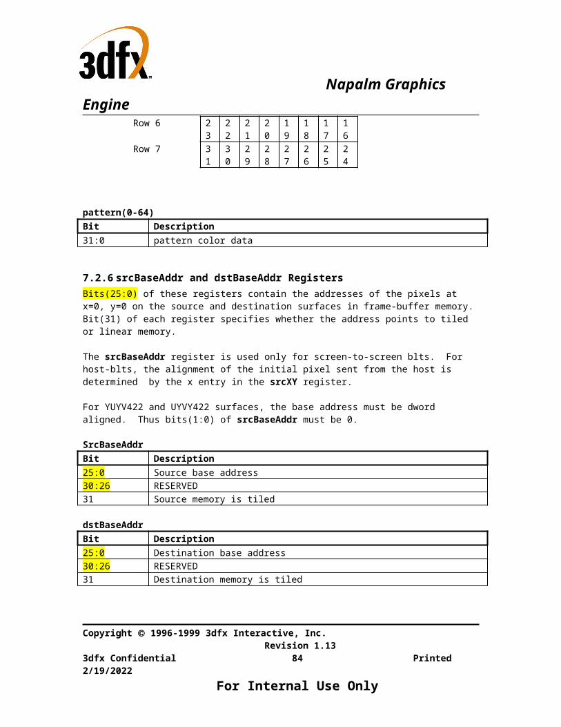
Napalm Graphics Engine
startB 0x028(40) 0xA 23:0 FBI W No / Yes Starting Blue parameter (12.12 format)startZ 0x02c(44) 0xB 31:0 FBI W No / Yes Starting Z parameter (20.12 or 28.4 format)startA 0x030(48) 0xC 23:0 FBI W No / Yes Starting Alpha parameter (12.12 format)startS 0x034(52) 0xD 31:0 TREX* W No / Yes Starting S/W parameter (14.18 format)startT 0x038(56) 0xE 31:0 TREX* W No / Yes Starting T/W parameter (14.18 format)startW 0x03c(60) 0xF 31:0 FBI+TREX* W No / Yes Starting 1/W parameter (2.30 format)
dRdX 0x040(64) 0x10 23:0 FBI W No / Yes Change in Red with respect to X (12.12 format)dGdX 0x044(68) 0x11 23:0 FBI W No / Yes Change in Green with respect to X (12.12 format)dBdX 0x048(72) 0x12 23:0 FBI W No / Yes Change in Blue with respect to X (12.12 format)dZdX 0x04c(76) 0x13 31:0 FBI W No / Yes Change in Z with respect to X (20.12 or 28.4
format)dAdX 0x050(80) 0x14 23:0 FBI W No / Yes Change in Alpha with respect to X (12.12 format)dSdX 0x054(84) 0x15 31:0 TREX* W No / Yes Change in S/W with respect to X (14.18 format)dTdX 0x058(88) 0x16 31:0 TREX* W No / Yes Change in T/W with respect to X (14.18 format)dWdX 0x05c(92) 0x17 31:0 FBI+TREX* W No / Yes Change in 1/W with respect to X (2.30 format)
dRdY 0x060(96) 0x18 23:0 FBI W No / Yes Change in Red with respect to Y (12.12 format)dGdY 0x064(100) 0x19 23:0 FBI W No / Yes Change in Green with respect to Y (12.12 format)dBdY 0x068(104) 0x1A 23:0 FBI W No / Yes Change in Blue with respect to Y (12.12 format)dZdY 0x06c(108) 0x1B 31:0 FBI W No / Yes Change in Z with respect to Y (20.12 or 28.4
format)dAdY 0x070(112) 0x1C 23:0 FBI W No / Yes Change in Alpha with respect to Y (12.12 format)dSdY 0x074(116) 0x1D 31:0 TREX* W No / Yes Change in S/W with respect to Y (14.18 format)dTdY 0x078(120) 0x1E 31:0 TREX* W No / Yes Change in T/W with respect to Y (14.18 format)dWdY 0x07c(124) 0x1F 31:0 FBI+TREX* W No / Yes Change in 1/W with respect to Y (2.30 format)
triangleCMD 0x080(128) 0x20 31 FBI+TREX% W No / Yes Execute TRIANGLE command (floating point)reserved 0x084(132) 0x21 n/a n/a W n/afvertexAx 0x088(136) 0x22 31:0 FBI+TREX% W No / Yes Vertex A x-coordinate location (floating point)fvertexAy 0x08c(140) 0x23 31:0 FBI+TREX% W No / Yes Vertex A y-coordinate location (floating point)fvertexBx 0x090(144) 0x24 31:0 FBI+TREX% W No / Yes Vertex B x-coordinate location (floating point)fvertexBy 0x094(148) 0x25 31:0 FBI+TREX% W No / Yes Vertex B y-coordinate location (floating point)fvertexCx 0x098(152) 0x26 31:0 FBI+TREX% W No / Yes Vertex C x-coordinate location (floating point)fvertexCy 0x09c(156) 0x27 31:0 FBI+TREX% W No / Yes Vertex C y-coordinate location (floating point)
fstartR 0x0a0(160) 0x28 31:0 FBI W No / Yes Starting Red parameter (floating point)fstartG 0x0a4(164) 0x29 31:0 FBI W No / Yes Starting Green parameter (floating point)fstartB 0x0a8(168) 0x2A 31:0 FBI W No / Yes Starting Blue parameter (floating point)fstartZ 0x0ac(172) 0x2B 31:0 FBI W No / Yes Starting Z parameter (floating point)fstartA 0x0b0(176) 0x2C 31:0 FBI W No / Yes Starting Alpha parameter (floating point)fstartS 0x0b4(180) 0x2D 31:0 TREX* W No / Yes Starting S/W parameter (floating point)fstartT 0x0b8(184) 0x2E 31:0 TREX* W No / Yes Starting T/W parameter (floating point)fstartW 0x0bc(188) 0x2F 31:0 FBI+TREX* W No / Yes Starting 1/W parameter (floating point)
fdRdX 0x0c0(192) 0x30 31:0 FBI W No / Yes Change in Red with respect to X (floating point)fdGdX 0x0c4(196) 0x31 31:0 FBI W No / Yes Change in Green with respect to X (floating point)fdBdX 0x0c8(200) 0x32 31:0 FBI W No / Yes Change in Blue with respect to X (floating point)fdZdX 0x0cc(204) 0x33 31:0 FBI W No / Yes Change in Z with respect to X (floating point)fdAdX 0x0d0(208) 0x34 31:0 FBI W No / Yes Change in Alpha with respect to X (floating point)fdSdX 0x0d4(212) 0x35 31:0 TREX* W No / Yes Change in S/W with respect to X (floating point)fdTdX 0x0d8(216) 0x36 31:0 TREX* W No / Yes Change in T/W with respect to X (floating point)fdWdX 0x0dc(220) 0x37 31:0 FBI+TREX* W No / Yes Change in 1/W with respect to X (floating point)
fdRdY 0x0e0(224) 0x38 31:0 FBI W No / Yes Change in Red with respect to Y (floating point)fdGdY 0x0e4(228) 0x39 31:0 FBI W No / Yes Change in Green with respect to Y (floating point)fdBdY 0x0e8(232) 0x3A 31:0 FBI W No / Yes Change in Blue with respect to Y (floating point)fdZdY 0x0ec(236) 0x3B 31:0 FBI W No / Yes Change in Z with respect to Y (floating point)fdAdY 0x0f0(240) 0x3C 31:0 FBI W No / Yes Change in Alpha with respect to Y (floating point)fdSdY 0x0f4(244) 0x3D 31:0 TREX* W No / Yes Change in S/W with respect to Y (floating point)fdTdY 0x0f8(248) 0x3E 31:0 TREX* W No / Yes Change in T/W with respect to Y (floating point)fdWdY 0x0fc(252) 0x3F 31:0 FBI+TREX* W No / Yes Change in 1/W with respect to Y (floating point)
Copyright 1996-1999 3dfx Interactive, Inc. Revision 1.133dfx Confidential 84 Printed 5/7/2023
For Internal Use Only
Napalm Graphics Engine
ftriangleCMD 0x100(256) 0x40 31 FBI+TREX% W No / Yes Execute TRIANGLE command (floating point)fbzColorPath 0x104(260) 0x41 31:0 FBI+TREX% R/W No / Yes FBI Color Path ControlfogMode 0x108(264) 0x42 15:0 FBI R/W No / Yes Fog Mode ControlalphaMode 0x10c(268) 0x43 31:0 FBI R/W No / Yes Alpha Mode ControlfbzMode 0x110(272) 0x44 21:0 FBI R/W Yes / Yes RGB Buffer and Depth-Buffer ControllfbMode 0x114(276) 0x45 16:0 FBI R/W Yes / Yes Linear Frame Buffer Mode ControlclipLeftRight 0x118(280) 0x46 31:0 FBI R/W Yes / Yes Left and Right of Clipping Register clipTopBottom 0x11c(284) 0x47 31:0 FBI R/W Yes / Yes Top and Bottom of Clipping Register
nopCMD 0x120(288) 0x48 1:0 FBI+TREX* W Yes/Yes Execute NOP commandfastfillCMD 0x124(292) 0x49 na FBI W Yes/Yes Execute FASTFILL commandswapbufferCMD 0x128(296) 0x4A 10:0 FBI W Yes/Yes Execute SWAPBUFFER commandfogColor 0x12c(300) 0x4B 23:0 FBI W Yes / Yes Fog Color ValuezaColor 0x130(304) 0x4C 31:0 FBI W Yes / Yes Constant Alpha/Depth ValuechromaKey 0x134(308) 0x4D 31:0 FBI W Yes / Yes Chroma Key Compare ValuechromaRange 0x138(312) 0x4E 31:0 FBI W Yes / Yes Chroma Range Compare Values, Modes & EnableuserIntrCMD 0x13c(316) 0x4F 9:0 FBI W Yes / Yes Execute USERINTERRUPT commandstipple 0x140(320) 0x50 31:0 FBI R/W Yes / Yes Rendering Stipple Valuecolor0 0x144(324) 0x51 31:0 FBI R/W Yes / Yes Constant Color #0color1 0x148(328) 0x52 31:0 FBI R/W Yes / Yes Constant Color #1
fbiPixelsIn 0x14c(332) 0x53 23:0 FBI R n/a Pixel Counter (Number pixels processed)fbiChromaFail 0x150(336) 0x54 23:0 FBI R n/a Pixel Counter (Number pixels failed Chroma test)fbiZfuncFail 0x154(340) 0x55 23:0 FBI R n/a Pixel Counter (Number pixels failed Z test)fbiAfuncFail 0x158(344) 0x56 23:0 FBI R n/a Pixel Counter (Number pixels failed Alpha test)fbiPixelsOut 0x15c(348) 0x57 23:0 FBI R n/a Pixel Counter (Number pixels drawn)
fogTable 0x160(352)to0x1dc(476)
0x58 to 0x77
31:0 FBI W Yes / Yes Fog Table
renderMode 0x1e0(480) 0x78 20:0 FBI R/W Yes / Yes Render Mode ControlstencilMode 0x1e4(484) 0x79 27:0 FBI R/W Yes / Yes Stencil Mode ControlstencilOp 0x1e8(488) 0x7A 11:0 FBI R/W Yes / Yes Stencil Operation ControlcolBufferAddr 0x1ec(492) 0x7B 31:0 FBI R/W Yes / Yes Color Buffer Base AddresscolBufferStride 0x1f0(496) 0x7C 15:0 FBI R/W Yes / Yes Color Buffer Stride, Memory typeauxBufferAddr 0x1f4(500) 0x7D 31:0 FBI R/W Yes / Yes Auxiliary Buffer Base AddressauxBufferStride 0x1f8(504) 0x7E 15:0 FBI R/W Yes / Yes Auxiliary Buffer Stride, Memory typefbiStenciltestFail 0x1fc(508) 0x7F 23:0 FBI R n/a Pixel Counter (Number pixels failed stencil test)
clipLeftRight1 0x200(512) 0x80 31:0 FBI R/W Yes / Yes Secondary Left/Right Clipping RegisterclipTopBottom1 0x204(516) 0x81 31:0 FBI R/W Yes / Yes Secondary Top/Bottom Clipping RegistercombineMode 0x208(520) 0x82 31:0 FBI+TREX* W No / Yes Combine Unit ControlssliCtrl 0x20c(524) 0x83 31:0 FBI+TREX* W Yes / Yes SLI Render ControlaaCtrl 0x210(528) 0x84 31:0 FBI+TREX* W Yes / Yes Anti-Aliasing ControlchipMask 0x214(532) 0x85 31:0 FBI+TREX% W Yes / Yes Chip Masking ControlleftDesktopBuf 0x218(536) 0x86 31:0 FBI W No / Yes Left Desktop addressreserved 0x21c(540)
to0x24b(587)
0x87 to 0x92
n/a n/a n/a n/a
swapPending 0x24c(588) 0x93 na FBI W No / No Swap buffer pendingleftOverlayBuf 0x250(592) 0x94 31:0 FBI W No / Yes Left Overlay addressrightOverlayBuf 0x254(596) 0x95 25:0 FBI W No / Yes Right Overlay addressfbiSwapHistory 0x258(600) 0x96 31:0 FBI R n/a Swap History RegisterfbiTrianglesOut 0x25c(604) 0x97 23:0 FBI R n/a Triangle Counter (Number triangles drawn)sSetupMode 0x260(608) 0x98 19:0 FBI W No / Yes Triangle setup modesVx 0x264(612) 0x99 31:0 FBI+TREX* W No / Yes Triangle setup XsVy 0x268(616) 0x9A 31:0 FBI+TREX* W No / Yes Triangle setup YsARGB 0x26c(620) 0x9B 31:0 FBI+TREX* W No / Yes Triangle setup Alpha, Red, Green, BluesRed 0x270(624) 0x9C 31:0 FBI W No / Yes Triangle setup Red valuesGreen 0x274(628) 0x9D 31:0 FBI W No / Yes Triangle setup Green value
Copyright 1996-1999 3dfx Interactive, Inc. Revision 1.133dfx Confidential 85 Printed 5/7/2023
For Internal Use Only
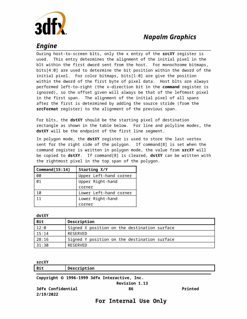
Napalm Graphics Engine
sBlue 0x278(632) 0x9E 31:0 FBI W No / Yes Triangle setup Blue valuesAlpha 0x27c(636) 0x9F 31:0 FBI W No / Yes Triangle setup Alpha valuesVz 0x280(640) 0xA0 31:0 FBI W No / Yes Triangle setup ZsWb 0x284(644) 0xA1 31:0 FBI+TREX* W No / Yes Triangle setup Global WsWtmu0 0x288(648) 0xA2 31:0 TREX* W No / Yes Triangle setup TREX0 & TREX1 WsS/W0 0x28c(652) 0xA3 31:0 TREX* W No / Yes Triangle setup TREX0 & TREX1 S/WsT/W0 0x290(656) 0xA4 31:0 TREX* W No / Yes Triangle setup TREX0 & TREX1 T/WsWtmu1 0x294(660) 0xA5 31:0 TREX* W No / Yes Triangle setup TREX1 only WsS/Wtmu1 0x298(664) 0xA6 31:0 TREX* W No / Yes Triangle setup TREX1 only S/WsT/Wtmu1 0x29c(668) 0xA7 31:0 TREX* W No / Yes Triangle setup TREX1 only T/WsDrawTriCMD 0x2a0(672) 0xA8 31:0 FBI+TREX* W No / Yes Triangle setup (Draw)sBeginTriCMD 0x2a4(676) 0xA9 31:0 FBI W No / Yes Triangle setup Start New triangle
reserved 0x2a8(680)to0x2fc(764)
0xAA to 0xBF
n/a n/a n/a n/a
textureMode 0x300(768) 0xC0 30:0 TREX* W No / Yes Texture Mode ControltLOD 0x304(772) 0xC1 23:0 TREX* W No / Yes Texture LOD SettingstDetail 0x308(776) 0xC2 21:0 TREX* W No / Yes Texture Detail SettingstexBaseAddr 0x30c(780) 0xC3 31:0 TREX* W No / Yes Texture Base AddresstexBaseAddr_1 0x310(784) 0xC4 25:0 TREX* W No / Yes Texture Base Address (supplemental LOD 1)texBaseAddr_2 0x314(788) 0xC5 25:0 TREX* W No / Yes Texture Base Address (supplemental LOD 2)texBaseAddr_3_8 0x318(792) 0xC6 25:0 TREX* W No / Yes Texture Base Address (supplemental LOD 3-8)texStride 0x31c(796) 0xC7trexInit1 0x320(800) 0xC8 31:0 TREX* W Yes / Yes TREX Hardware Initialization (register 1
nccTable0 0x324(804)to 0x350(848)
0xC9 to 0xD4
31:0or26:0
TREX* W Yes / Yes Narrow Channel Compression Table 0 (12 entries)
nccTable1 0x354(852)to0x380(896)
0xD5 tp 0xE0
31:0 or 26:0
TREX* W Yes / Yes Narrow Channel Compression Table 1 (12 entries)
reserved 0x384(900)to0x3fc(1020)
0xE1 to 0xFF
n/a n/a n/a n/a
The triangle parameter registers are aliased to a different address mapping to improve PCI bus throughput. The upper bit of the wrap field in the pci address is 0x1 (pci_ad[21]=1), the following table shows the addresses for the triangle parameter registers.
Register Name Address Reg Num
Bits Chip R/W
Sync? /Fifo?
Description
status 0x000(0) 0x0 31:0 FBI R/W No / Yes SST-1 StatusintrCtrl 0x004(4) 0x1 19:0 FBI R/W No / No Interrupt Status and ControlvertexAx 0x008(8) 0x2 15:0 FBI+TREX% W No / Yes Vertex A x-coordinate location (12.4 format)vertexAy 0x00c(12) 0x3 15:0 FBI+TREX% W No / Yes Vertex A y-coordinate location (12.4 format)vertexBx 0x010(16) 0x4 15:0 FBI+TREX% W No / Yes Vertex B x-coordinate location (12.4 format)vertexBy 0x014(20) 0x5 15:0 FBI+TREX% W No / Yes Vertex B y-coordinate location (12.4 format)vertexCx 0x018(24) 0x6 15:0 FBI+TREX% W No / Yes Vertex C x-coordinate location (12.4 format)vertexCy 0x01c(28) 0x7 15:0 FBI+TREX% W No / Yes Vertex C y-coordinate location (12.4 format)
startR 0x020(32) 0x8 23:0 FBI W No / Yes Starting Red parameter (12.12 format)dRdX 0x024(36) 0x9 23:0 FBI W No / Yes Change in Red with respect to X (12.12 format)dRdY 0x028(40) 0xA 23:0 FBI W No / Yes Change in Red with respect to Y (12.12 format)startG 0x02c(44) 0xB 23:0 FBI W No / Yes Starting Green parameter (12.12 format)dGdX 0x030(48) 0xC 23:0 FBI W No / Yes Change in Green with respect to X (12.12 format)dGdY 0x034(52) 0xD 23:0 FBI W No / Yes Change in Green with respect to Y (12.12 format)
Copyright 1996-1999 3dfx Interactive, Inc. Revision 1.133dfx Confidential 86 Printed 5/7/2023
For Internal Use Only

Napalm Graphics Engine startB 0x038(56) 0xE 23:0 FBI W No / Yes Starting Blue parameter (12.12 format)dBdX 0x03c(60) 0xF 23:0 FBI W No / Yes Change in Blue with respect to X (12.12 format)dBdY 0x040(64) 0x10 23:0 FBI W No / Yes Change in Blue with respect to Y (12.12 format)startZ 0x044(68) 0x11 31:0 FBI W No / Yes Starting Z parameter (20.12 format)dZdX 0x048(72) 0x12 31:0 FBI W No / Yes Change in Z with respect to X (20.12 format)dZdY 0x04c(76) 0x13 31:0 FBI W No / Yes Change in Z with respect to Y (12.12 format)startA 0x050(80) 0x14 23:0 FBI W No / Yes Starting Alpha parameter (12.12 format)dAdX 0x054(84) 0x15 23:0 FBI W No / Yes Change in Alpha with respect to X (12.12 format)dAdY 0x058(88) 0x16 23:0 FBI W No / Yes Change in Alpha with respect to Y (12.12 format)startS 0x05c(92) 0x17 31:0 TREX* W No / Yes Starting S/W parameter (14.18 format)dSdX 0x060(96) 0x18 31:0 TREX* W No / Yes Change in S/W with respect to X (14.18 format)dSdY 0x064(100) 0x19 31:0 TREX* W No / Yes Change in S/W with respect to Y (14.18 format)startT 0x068(104) 0x1A 31:0 TREX* W No / Yes Starting T/W parameter (14.18 format)dTdX 0x06c(108) 0x1B 31:0 TREX* W No / Yes Change in T/W with respect to X (14.18 format)dTdY 0x070(112) 0x1C 31:0 TREX* W No / Yes Change in T/W with respect to Y (14.18 format)startW 0x074(116) 0x1D 31:0 FBI+TREX* W No / Yes Starting 1/W parameter (2.30 format)dWdX 0x078(120) 0x1E 31:0 FBI+TREX* W No / Yes Change in 1/W with respect to X (2.30 format)dWdY 0x07c(124) 0x1F 31:0 FBI+TREX* W No / Yes Change in 1/W with respect to Y (2.30 format)
triangleCMD 0x080(128) 0x20 31 FBI+TREX% W No / Yes Execute TRIANGLE command (sign bit)reserved 0x084(132) 0x21 n/a n/a W n/afvertexAx 0x088(136) 0x22 31:0 FBI+TREX% W No / Yes Vertex A x-coordinate location (floating point)fvertexAy 0x08c(140) 0x23 31:0 FBI+TREX% W No / Yes Vertex A y-coordinate location (floating point)fvertexBx 0x090(144) 0x24 31:0 FBI+TREX% W No / Yes Vertex B x-coordinate location (floating point)fvertexBy 0x094(148) 0x25 31:0 FBI+TREX% W No / Yes Vertex B y-coordinate location (floating point)fvertexCx 0x098(152) 0x26 31:0 FBI+TREX% W No / Yes Vertex C x-coordinate location (floating point)fvertexCy 0x09c(156) 0x27 31:0 FBI+TREX% W No / Yes Vertex C y-coordinate location (floating point)
fstartR 0x0a0(160) 0x28 31:0 FBI W No / Yes Starting Red parameter (floating point)fdRdX 0x0a4(164) 0x29 31:0 FBI W No / Yes Change in Red with respect to X (floating point)fdRdY 0x0a8(168) 0x2A 31:0 FBI W No / Yes Change in Red with respect to Y (floating point)fstartG 0x0ac(172) 0x2B 31:0 FBI W No / Yes Starting Green parameter (floating point)fdGdX 0x0b0(176) 0x2C 31:0 FBI W No / Yes Change in Green with respect to X (floating point)fdGdY 0x0b4(180) 0x2D 31:0 FBI W No / Yes Change in Green with respect to Y (floating point)fstartB 0x0b8(184) 0x2E 31:0 FBI W No / Yes Starting Blue parameter (floating point)fdBdX 0x0bc(188) 0x2F 31:0 FBI W No / Yes Change in Blue with respect to X (floating point)fdBdY 0x0c0(192) 0x30 31:0 FBI W No / Yes Change in Blue with respect to Y (floating point)fstartZ 0x0c4(196) 0x31 31:0 FBI W No / Yes Starting Z parameter (floating point)fdZdX 0x0c8(200) 0x32 31:0 FBI W No / Yes Change in Z with respect to X (floating point)fdZdY 0x0cc(204) 0x33 31:0 FBI W No / Yes Change in Z with respect to Y (floating point)fstartA 0x0d0(208) 0x34 31:0 FBI W No / Yes Starting Alpha parameter (floating point)fdAdX 0x0d4(212) 0x35 31:0 FBI W No / Yes Change in Alpha with respect to X (floating point)fdAdY 0x0d8(216) 0x36 31:0 FBI W No / Yes Change in Alpha with respect to Y (floating point)fstartS 0x0dc(220) 0x37 31:0 TREX* W No / Yes Starting S/W parameter (floating point)fdSdX 0x0e0(224) 0x38 31:0 TREX* W No / Yes Change in S/W with respect to X (floating point)fdSdY 0x0e4(228) 0x39 31:0 TREX* W No / Yes Change in S/W with respect to Y (floating point)fstartT 0x0e8(232) 0x3A 31:0 TREX* W No / Yes Starting T/W parameter (floating point)fdTdX 0x0ec(236) 0x3B 31:0 TREX* W No / Yes Change in T/W with respect to X (floating point)fdTdY 0x0f0(240) 0x3C 31:0 TREX* W No / Yes Change in T/W with respect to Y (floating point)fstartW 0x0f4(244) 0x3D 31:0 FBI+TREX* W No / Yes Starting 1/W parameter (floating point)fdWdX 0x0f8(248) 0x3E 31:0 FBI+TREX* W No / Yes Change in 1/W with respect to X (floating point)fdWdY 0x0fc(252) 0x3F 31:0 FBI+TREX* W No / Yes Change in 1/W with respect to Y (floating point)
ftriangleCMD 0x100(256) 0x40 31 FBI+TREX% W No / Yes Execute TRIANGLE command (floating point)
Copyright 1996-1999 3dfx Interactive, Inc. Revision 1.133dfx Confidential 87 Printed 5/7/2023
For Internal Use Only

Napalm Graphics Engine
8.1 status RegisterThe status register provides a way for the CPU to interrogate the graphics processor about its current state and FIFO availability. The status register is read only, but writing to status clears any Napalm generated PCI interrupts.
Bit Description4:0 PCI FIFO freespace (0x1f=FIFO empty). Default is 0x1f.5 PCI FIFO Busy6 Vertical retrace (0=Vertical retrace active, 1=Vertical retrace inactive)7 FBI graphics engine busy (0=engine idle, 1=engine busy)8 TREX busy (0=engine idle, 1=engine busy)9 Napalm busy (0=idle, 1=busy)10 2D busy (0=idle, 1=busy)11 CMDFIFO Unit #0 busy (0=idle, 1=busy)12 CMDFIFO Unit #1 busy (0=idle, 1=busy)13 TREX #0 busy (0=idle, 1=busy)14 TREX #1 busy (0=idle, 1=busy)27:15 reserved30:28 Swap Buffers Pending. Default is 0x0.31 PCI Interrupt Generated (1=interrupt generated)
Bits(5:0) show the number of entries available in the internal host FIFO. The internal host FIFO is 64 entries deep. The FIFO is empty when bits(5:0)=0x3f. Bit(6) is the state of the monitor vertical retrace signal, and is used to determine when the monitor is being refreshed. Bit(7) of status is used to determine if the graphics engine of FBI is active. Note that bit(7) only determines if the graphics engine of FBI is busy -- it does not include information as to the status of the internal PCI FIFOs. Bit(8) of status is used to determine if TREX is busy. Note that bit(8) of status is set if any unit in TREX is not idle -- this includes the graphics engine and all internal TREX FIFOs. Bit(9) of status determines if all units in the Napalm system (including graphics engines, FIFOs, etc.) are idle. Bit(9) is set when any internal unit in Napalm is active (e.g. graphics is being rendered or any FIFO is not empty). When the Memory FIFO is enabled, bits(27:12) show the number of entries available in the Memory FIFO. Depending upon the amount of frame buffer memory available, a maximum of 65,536 entries may be stored in the Memory FIFO. The Memory FIFO is empty when bits(27:12)=0xffff. Bits (30:28) of status track the number of outstanding SWAPBUFFER commands. When a SWAPBUFFER command is received from the host cpu, bits (30:28) are incremented -- when a SWAPBUFFER command completes, bits (30:28) are decremented. Bit(31) of status is used to monitor the status of the PCI interrupt signal. If Napalm generates a vertical retrace interrupt (as defined in pciInterrupt), bit(31) is set and the PCI interrupt signal line is activated to generate a hardware interrupt. An interrupt is cleared by writing to status with “dont-care” data. NOTE THAT BIT(31) IS CURRENTLY NOT IMPLEMENTED IN HARDWARE, AND WILL ALWAYS RETURN 0X0.
8.2 intrCtrl RegisterThe intrCtrl register controls the interrupt capabilities of Napalm. Bits 1:0 enable video horizontal sync signal generation of interrupts. Generated horizontal sync interrupts are detected by the CPU by reading bits 7:6 of intrCtrl. Bits 3:2 enable video vertical sync signal generation of interrupts. Generated vertical sync interrupts are detected by the CPU by reading bits 9:8 of intrCtrl. Bit 4 of intrCtrl enables generation of interrupts when the frontend PCI FIFO is full. Generated PCI FIFO Full interrupts are detected by the CPU by reading bit 10 of intrCtrl. PCI FIFO full interrupts are genered when intrCtrl Copyright 1996-1999 3dfx Interactive, Inc. Revision 1.133dfx Confidential 88 Printed 5/7/2023
For Internal Use Only

Napalm Graphics Engine bit 4 is set and the number of free entries in the frontend PCI FIFO drops below the value specified in fbiInit0 bits(10:6). Bit 5 of intrCtrl enables the user interrupt command USERINTERRUPT generation of interrupts. Generated user interrupts are detected by the CPU by reading bit 11 of intrCtrl. The tag associated with a generated user interrupt is stored in bits 19:12 of intrCtrl.
Generated interrupts are cleared by writing a 0 to the bit signaling a particular interrupt was generated and writing a 1 to interCtrl bit(31). For example, a PCI FIFO full generated interrupt is cleared by writing a 0 to bit 10 of intrCtrl, and a generated user interrupt is cleared by writing a 0 to bit 11 of intrCtrl. For both cases, bit 31 of intrCtrl must be written with the value 1 to clear the external PCI interrupt. Care must be taken when clearing interrupts not to accidentally overwrite the interrupt mask bits (bits 5:0) of intrCtrl) which enable generation of particular interrupts.
Note that writes to the intrCtrl register are not pushed on the PCI frontend FIFO, so writes to intrCtrl are processed immediately. Since intrCtrl is not FIFO’ed, writes to intrCtrl may be processed out-of-order with respect to other queued writes in the PCI and memory-backed FIFOs.
Bit Description0 Horizontal Sync (rising edge) interrupts enable (1=enable). Default is 0.1 Horizontal Sync (falling edge) interrupts enable (1=enable). Default is 0.2 Vertical Sync (rising edge) interrupts enable (1=enable). Default is 0.3 Vertical Sync (falling edge) interrupts enable (1=enable). Default is 0.4 PCI FIFO Full interrupts enable (1=enable). Default is 0.5 User Interrupt Command interrupts enable (1=enable). Default is 0.6 Horizontal Sync (rising edge) interrupt generated (1=interrupt generated).7 Horizontal Sync (falling edge) interrupt generated (1=interrupt generated).8 Vertical Sync (rising edge) interrupt generated (1=interrupt generated).9 Vertical Sync (falling edge) interrupt generated (1=interrupt generated).10 PCI FIFO Full interrupt generated (1=interrupt generated).11 User Interrupt Command interrupt generated (1=interrupt generated).19:12 User Interrupt Command Tag. Read only.20 Hole counting interupts enable (1=enable). Default is 0.21 VMI interrupts enable. (1=enable). Default is 0.22 Hole counting interrupt generated (1=interrupt generated).23 VMI interrupt generated (1=interrupt generated).24 iMatch Counter timeout interrupts enabled. (1=enable). Default is 0.25 iMatch Counter timeout interrupt generated (1=interrupt generated).26 hotplug interrupt enable (1=enable). Default is 0. Note that both edges of the hotplug
input signal will cause an interrupt – this lets software decide what to do in both cases. Also note that the current status of the hotplug signal pin is determined by reading cfgSliAaMisc bit(11).
27 hotplug interrupt generated (1=interrupt generated)29:28 reserved30 VGA Interrupt generated (1=interrupt generated).31 External pin pci_inta value, active low (0=PCI interrupt is active, 1=PCI interrupt is
inactive)
8.3 vertex and fvertex RegistersThe vertexAx, vertexAy, vertexBx, vertexBy, vertexCx, vertexCy, fvertexAx, fvertexAy, fvertexBx, fvertexBy, fvertexCx, and fvertexCy registers specify the x and y coordinates of a triangle to be
Copyright 1996-1999 3dfx Interactive, Inc. Revision 1.133dfx Confidential 89 Printed 5/7/2023
For Internal Use Only

Napalm Graphics Engine rendered. There are three vertices in an Napalm triangle, with the AB and BC edges defining the minor edge and the AC edge defining the major edge. The diagram below illustrates two typical triangles:
(vertexAx, vertexAy)
(vertexBx, vertexBy)
(vertexCx, vertexCy)
Major Edge
Minor Edge
Minor Edge
(vertexAx, vertexAy)
(vertexBx, vertexBy)
(vertexCx, vertexCy)
Major Edge
Minor Edge
Minor Edge
The fvertex registers are floating point equivalents of the vertex registers. Napalm automatically converts both the fvertex and vertex registers into an internal fixed point notation used for rendering.
vertexAx, vertexAy, vertexBx, vertexBy, vertexCx, vertexCyBit Description15:0 Vertex coordinate information (fixed point two’s complement 12.4 format)
fvertexAx, fvertexAy, fvertexBx, fvertexBy, fvertexCx, fvertexCyBit Description31:0 Vertex coordinate information (IEEE 32-bit single-precision floating point format)
8.4 startR, startG, startB, startA, fstartR, fstartG, fstartB, and fstartA RegistersThe startR, startG, startB, startA, fstartR, fstartG, fstartB, and fstartA registers specify the starting color information (red, green, blue, and alpha) of a triangle to be rendered. The start registers must contain the color values associated with the A vertex of the triangle. The fstart registers are floating point equivalents of the start registers. Napalm automatically converts both the start and fstart registers into an internal fixed point notation used for rendering.
startR, startG, startB, startABit Description23:0 Starting Vertex-A Color information (fixed point two’s complement 12.12 format)
fstartR, fstartG, fstartB, fstartABit Description31:0 Starting Vertex-A Color information (IEEE 32-bit single-precision floating point
format)
8.5 startZ and fstartZ registersThe startZ and fstartZ registers specify the starting Z information of a triangle to be rendered. The startZ registers must contain the Z values associated with the A vertex of the triangle. The fstartZ register is a floating point equivalent of the startZ registers. Napalm automatically converts both the
Copyright 1996-1999 3dfx Interactive, Inc. Revision 1.133dfx Confidential 90 Printed 5/7/2023
For Internal Use Only

Napalm Graphics Engine startZ and fstartZ registers into an internal fixed point notation used for rendering. Note that the incoming format assumed for the startZ register is dependent on the rendering mode selected – when 32-bit rendering is enabled (renderMode[1:0]=0x2) then the startZ register is assumed to be in a 28.4 format, otherwise the startZ register is assumed to be in a 20.12 format.
startZBit Description31:0 Starting Vertex-A Z information (fixed point two’s complement 20.12 or 28.4 format)
fstartZBit Description31:0 Starting Vertex-A Z information (IEEE 32-bit single-precision floating point format)
8.6 startS, startT, fstartS, and fstartT RegistersThe startS, startT, fstartS, and fstartT registers specify the starting S/W and T/W texture coordinate information of a triangle to be rendered. The start registers must contain the texture coordinates associated with the A vertex of the triangle. Note that the S and T coordinates used by Napalm for rendering must be divided by W prior to being sent to Napalm (i.e. Napalm iterates S/W and T/W prior to perspective correction). During rendering, the iterated S and T coordinates are (optionally) divided by the iterated W parameter to perform perspective correction. The fstart registers are floating point equivalents of the start registers. Napalm automatically converts both the start and fstart registers into an internal fixed point notation used for rendering.
startS, startTBit Description31:0 Starting Vertex-A Texture coordinates (fixed point two’s complement 14.18 format)
fstartS, fstartTBit Description31:0 Starting Vertex-A Texture coordinates (IEEE 32-bit single-precision floating point
format)
8.7 startW and fstartW registersThe startW and fstartW registers specify the starting 1/W information of a triangle to be rendered. The startW registers must contain the W values associated with the A vertex of the triangle. Note that the W value used by Napalm for rendering is actually the reciprocal of the 3D-geometry-calculated W value (i.e. Napalm iterates 1/W prior to perspective correction). During rendering, the iterated S and T coordinates are (optionally) divided by the iterated W parameter to perform perspective correction. The fstartW register is a floating point equivalent of the startW registers. Napalm automatically converts both the startW and fstartW registers into an internal fixed point notation used for rendering.
startWBit Description31:0 Starting Vertex-A W information (fixed point two’s complement 2.30 format)
fstartWBit Description31:0 Starting Vertex-A W information (IEEE 32-bit single-precision floating point format)
Copyright 1996-1999 3dfx Interactive, Inc. Revision 1.133dfx Confidential 91 Printed 5/7/2023
For Internal Use Only
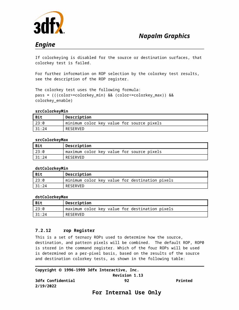
Napalm Graphics Engine 8.8 dRdX, dGdX, dBdX, dAdX, fdRdX, fdGdX, fdBdX, and fdAdX RegistersThe dRdX, dGdX, dBdX, dAdX, fdRdX, fdGdX, fdBdX, and fdAdX registers specify the change in the color information (red, green, blue, and alpha) with respect to X of a triangle to be rendered. As a triangle is rendered, the d?dX registers are added to the the internal color component registers when the pixel drawn moves from left-to-right, and are subtracted from the internal color component registers when the pixel drawn moves from right-to-left. The fd?dX registers are floating point equivalents of the d?dX registers. Napalm automatically converts both the d?dX and fd?dX registers into an internal fixed point notation used for rendering.
dRdX, dGdX, dBdX, dAdXBit Description23:0 Change in color with respect to X (fixed point two’s complement 12.12 format)
fdRdX, fdGdX, fdBdX, fdAdXBit Description31:0 Change in color with respect to X (IEEE 32-bit single-precision floating point format)
8.9 dZdX and fdZdX RegistersThe dZdX and fdZdX registers specify the change in Z with respect to X of a triangle to be rendered. As a triangle is rendered, the dZdX register is added to the the internal Z register when the pixel drawn moves from left-to-right, and is subtracted from the internal Z register when the pixel drawn moves from right-to-left. The fdZdX registers are floating point equivalents of the dZdX registers. Napalm automatically converts both the dZdX and fdZdX registers into an internal fixed point notation used for rendering. Note that the incoming format assumed for the dZdX and dZdY registers is dependent on the rendering mode selected – when 32-bit rendering is enabled (renderMode[1:0]=0x2) then the dZdX and dZdY registers are assumed to be in a 28.4 format, otherwise the dZdX and dZdY registers are assumed to be in a 20.12 format.
dZdXBit Description31:0 Change in Z with respect to X (fixed point two’s complement 20.12 or 28.4 format)
fdZdXBit Description31:0 Change in Z with respect to X (IEEE 32-bit single-precision floating point format)
8.10 dSdX, dTdX, fdSdX, and fdTdX RegistersThe dXdX, dTdX, fdSdX, and fdTdX registers specify the change in the S/W and T/W texture coordinates with respect to X of a triangle to be rendered. As a triangle is rendered, the d?dX registers are added to the the internal S and T registers when the pixel drawn moves from left-to-right, and are subtracted from the internal S/W and T/W registers when the pixel drawn moves from right-to-left. Note that the delta S/W and T/W values used by Napalm for rendering must be divided by W prior to being sent to Napalm (i.e. Napalm uses S/W and T/W ). The d?dX registers are floating point equivalents of the fd?dX registers. Napalm automatically converts both the d?dX and fd?dX registers into an internal fixed point notation used for rendering.
dSdX, dTdXBit Description
Copyright 1996-1999 3dfx Interactive, Inc. Revision 1.133dfx Confidential 92 Printed 5/7/2023
For Internal Use Only

Napalm Graphics Engine 31:0 Change in S and T with respect to X (fixed point two’s complement 14.18 format)
fdSdX, fdTdXBit Description31:0 Change in Z with respect to X (IEEE 32-bit single-precision floating point format)
8.11 dWdX and fdWdX RegistersThe dWdX and fdWdX registers specify the change in 1/W with respect to X of a triangle to be rendered. As a triangle is rendered, the dWdX register is added to the the internal 1/W register when the pixel drawn moves from left-to-right, and is subtracted from the internal 1/W register when the pixel drawn moves from right-to-left. The fdWdX registers are floating point equivalents of the dWdX registers. Napalm automatically converts both the dWdX and fdWdX registers into an internal fixed point notation used for rendering.
dWdXBit Description31:0 Change in W with respect to X (fixed point two’s complement 2.30 format)
fdWdXBit Description31:0 Change in W with respect to X (IEEE 32-bit single-precision floating point format)
8.12 dRdY, dGdY, dBdY, dAdY, fdRdY, fdGdY, fdBdY, and fdAdY RegistersThe dRdY, dGdY, dBdY, dAdY, fdRdY, fdGdY, fdBdY, and fdAdY registers specify the change in the color information (red, green, blue, and alpha) with respect to Y of a triangle to be rendered. As a triangle is rendered, the d?dY registers are added to the the internal color component registers when the pixel drawn in a positive Y direction, and are subtracted from the internal color component registers when the pixel drawn moves in a negative Y direction. The fd?dY registers are floating point equivalents of the d?dY registers. Napalm automatically converts both the d?dY and fd?dY registers into an internal fixed point notation used for rendering.
dRdY, dGdY, dBdY, dAdYBit Description23:0 Change in color with respect to Y (fixed point two’s complement 12.12 format)
fdRdY, fdGdY, fdBdY, fdAdYBit Description31:0 Change in color with respect to Y (IEEE 32-bit single-precision floating point format)
8.13 dZdY and fdZdY RegistersThe dZdY and fdZdY registers specify the change in Z with respect to Y of a triangle to be rendered. As a triangle is rendered, the dZdY register is added to the the internal Z register when the pixel drawn moves in a positive Y direction, and is subtracted from the internal Z register when the pixel drawn moves in a negative Y direction. The fdZdY registers are floating point equivalents of the dZdY registers. Napalm automatically converts both the dZdY and fdZdY registers into an internal fixed point notation used for rendering.
dZdY
Copyright 1996-1999 3dfx Interactive, Inc. Revision 1.133dfx Confidential 93 Printed 5/7/2023
For Internal Use Only
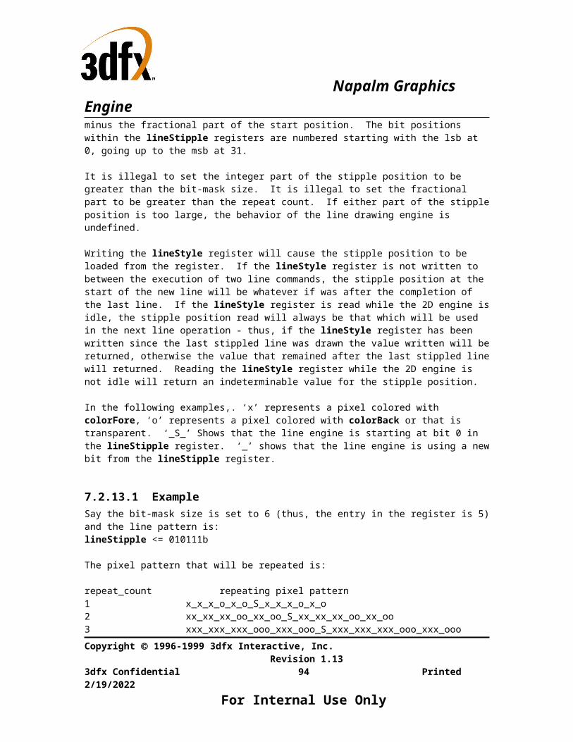
Napalm Graphics Engine Bit Description31:0 Change in Z with respect to Y (fixed point two’s complement 20.12 format)
fdZdYBit Description31:0 Change in Z with respect to Y (IEEE 32-bit single-precision floating point format)
8.14 dSdY, dTdY, fdSdY, and fdTdY RegistersThe dYdY, dTdY, fdSdY, and fdTdY registers specify the change in the S/W and T/W texture coordinates with respect to Y of a triangle to be rendered. As a triangle is rendered, the d?dY registers are added to the the internal S/W and T/W registers when the pixel drawn moves in a positive Y direction, and are subtracted from the internal S/W and T/W registers when the pixel drawn moves in a negative Y direction. Note that the delta S/W and T/W values used by Napalm for rendering must be divided by W prior to being sent to Napalm (i.e. Napalm uses S/W and T/W ). The d?dY registers are floating point equivalents of the fd?dY registers. Napalm automatically converts both the d?dY and fd?dY registers into an internal fixed point notation used for rendering.
dSdY, dTdYBit Description31:0 Change in S and T with respect to Y (fixed point two’s complement 14.18 format)
fdSdY, fdTdYBit Description31:0 Change in Z with respect to Y (IEEE 32-bit single-precision floating point format)
8.15 dWdY and fdWdY RegistersThe dWdY and fdWdY registers specify the change in 1/W with respect to Y of a triangle to be rendered. As a triangle is rendered, the dWdY register is added to the the internal 1/W register when the pixel drawn moves in a positive Y direction, and is subtracted from the internal 1/W register when the pixel drawn moves in a negative Y direction. The fdWdY registers are floating point equivalents of the dWdY registers. Napalm automatically converts both the dWdY and fdWdY registers into an internal fixed point notation used for rendering.
dWdYBit Description31:0 Change in W with respect to Y (fixed point two’s complement 2.30 format)
fdWdYBit Description31:0 Change in W with respect to Y (IEEE 32-bit single-precision floating point format)
8.16 triangleCMD and ftriangleCMD RegistersThe triangleCMD and ftriangleCMD registers execute the triangle drawing command. Writes to triangleCMD or ftriangleCMD initiate rendering a triangle defined by the vertex, start, d?dX, and d?dY registers. Note that the vertex, start, d?dX, and d?dY registers must be setup prior to writing to triangleCMD or ftriangleCMD. The value stored to triangleCMD or ftriangleCMD is the area of the triangle being rendered -- this value determines whether a triangle is clockwise or counter-clockwise geometrically. If bit(31)=0, then the triangle is oriented in a counter-clockwise orientation (i.e. positive
Copyright 1996-1999 3dfx Interactive, Inc. Revision 1.133dfx Confidential 94 Printed 5/7/2023
For Internal Use Only
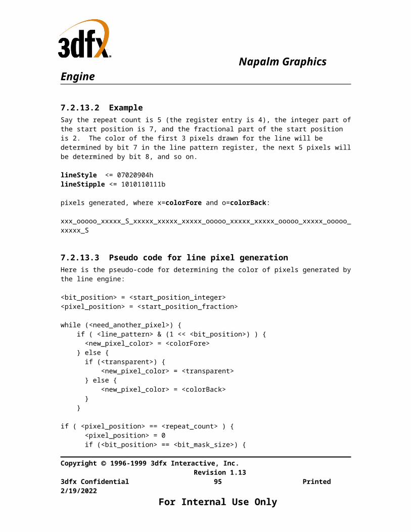
Napalm Graphics Engine area). If bit(31)=1, then the triangle is oriented in a clockwise orientation (i.e. negative area). To calculate the area of a triangle, the following steps are performed:
1. The vertices (A, B, and C) are sorted by the Y coordinate in order of increasing Y (i.e. A.y <= B.y <= C.y)
2. The area is calculated as follows:AREA = ((dxAB * dyBC) - (dxBC * dyAB)) / 2
wheredxAB = A.x - B.xdyBC = B.y - C.ydxBC = B.x - C.xdyAB = A.y - B.y
Note that Napalm only requires the sign bit of the area to be stored in the triangleCMD and ftriangleCMD registers -- bits(30:0) written to triangleCMD and ftriangleCMD are ignored.
triangleCMDBit Description31 Sign of the area of the triangle to be rendered
ftriangleCMDBit Description31 Sign of the area of the triangle to be rendered (IEEE 32-bit single-precision floating
point format)
8.17 nopCMD RegisterWriting any data to the nopCMD register executes the NOP command. Executing a NOP command flushes the graphics pipeline. The lsb of the data value written to nopCMD is used to optionally clear the fbiPixelsIn, fbiChromaFail, fbiZfuncFail, fbiAfuncFail, fbiPixelsOut, and fbiStenciltestFail registers. Writing a ‘1’ to the lsb of nopCMD will clear the aforementioned registers. Writing a ‘0’ to the lsb of nopCMD will not modify the values of the aforementioned registers. Similarly, nopCMD bit(1) is used to optionally clear the fbiTrianglesOut register.
Bit Description0 Clear fbiPixelsIn, fbiChromaFail, fbiZfuncFail, fbiAfuncFail, fbiPixelsOut and
fbiStenciltestFail registers (1=clear registers)1 Clear fbiTrianglesOut register (1=clears register)
8.18 fastfillCMD RegisterWriting any data to the fastfill register executes the FASTFILL command. The FASTFILL command is used to clear the RGB and depth buffers as quickly as possible. Prior to executing the FASTFILL command, the clipLeftRight and clipTopBottom are loaded with a rectangular area which is the desired area to be cleared. Note that clip registers define a rectangular area which is inclusive of the clipLeft and clipTop register values, but exclusive of the clipRight and clipBottom register values. The fastfillCMD register is then written to initiate the FASTFILL command after the clip registers have been loaded.
When running in 15 or 16 BPP rendering modes, FASTFILL will optionally clear the color buffers with the RGB color specified in color1[23:0], and also optionally clears the depth buffer with the depth value taken from zaColor[15:0] register. Note that since color1[23:0] is a 24-bit value, either dithering or bit Copyright 1996-1999 3dfx Interactive, Inc. Revision 1.133dfx Confidential 95 Printed 5/7/2023
For Internal Use Only
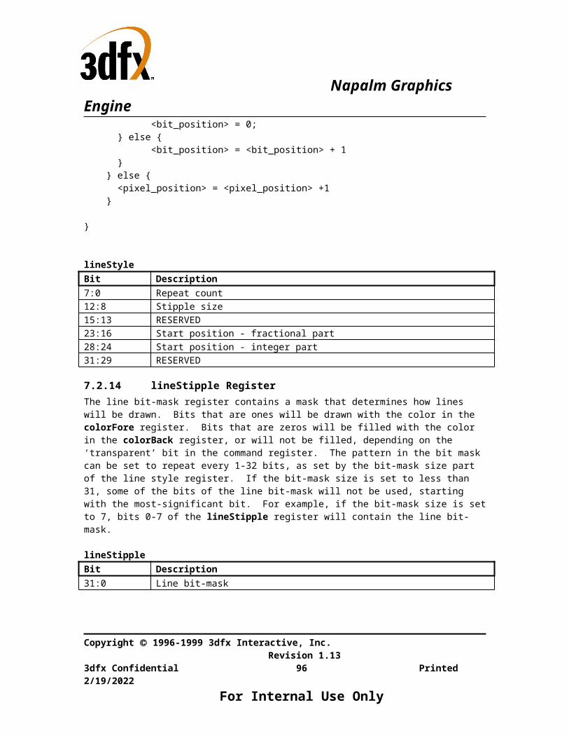
Napalm Graphics Engine truncation must be used to translate the 24-bit value into the native 16-bit frame buffer -- dithering may be employed optionally as defined by bit(8) of fbzMode. Disabling clearing of the color or depth buffers is accomplished by modifying the rgb/depth mask bits(10:9) in fbzMode. This allows individual or combined clearing of the RGB and depth buffers.
When running in 15 BPP rendering mode, the 1-bit alpha value stored into the frame buffer is calculated as follows:
- zaColor bit(31) if renderMode[16:15]=0x2- 1 if renderMode[16:15]=0x1- 0 if renderMode[16:15]=0x0
When using SGRAM, fastfillCMD[0] overrides fbzMode[8], and forces dithering off, allowing the color plane to be filled using SGRAM blockwrites. When using SDRAM, dithering behavior is determined solely by fbzMode[8].
When running in 32 BPP rendering modes FASTFILL will optionally clear the alpha and color buffers with the ARGB color specified in color1[31:0], and also optionally clear the stencil and depth buffers with the depth value taken from zaColor[23:0] and the stencil value taken from stencilMode[7:0]. Disabling clearing of the alpha and color buffers is accomplished by clearing fbzMode bit(9), while individual alpha and color planes may be selectively cleared by using renderMode bits(20:17). Similarly, disabling clearing of the depth buffer is accomplished by clearing fbzMode bit(10), and disabling clearing of the stencil buffer is accomplished by setting stencilMode bits(23:16) equal to 0x0. Note that the stencil buffer will be cleared when any of the bits of stencilMode bits(23:16) are set.
*** IMPORTANT NOTE: There are several bugs in the FASTFILL command when used in scanline interleave (SLI) configurations:
1. Performance. When using the FASTFILL command in SLI, fillrate performance should, at least in theory, increase by the number of chips used in the SLI configuration. However,a bug in the FASTFILL hardware logic does not allow such performance gains. As a result, the rendering performance of the FASTFILL command will always be equal to the single-chip FASTFILL fillrate, even if in an SLI configuration. This is true for both SDRAM and SGRAM memory configurations.
2. SGRAM memories and tiled surfaces. There is a bug in the FASTFILL hardware logic which causes pixels to be rendered improperly when in SLI configuration uses SGRAM memories and filling tiled surfaces.
To workaround these hardware bugs, it is recommend that software use the 2D BLT command to fill surfaces when in an SLI configuration.
Bit Description0 Disable dithering during fastfill (1 = disable dithering).
8.19 swapbufferCMD RegisterWriting to the swapbufferCMD register executes the SWAPBUFFER command. If the data written to swapbufferCMD bit(0)=0, then the frame buffer swapping is not synchronized with vertical retrace. If frame buffer swapping is not synchronized with vertical retrace, then visible frame “tearing” may occur. If swapbufferCMD bit(0)=1 then the frame buffer swapping is synchronized with vertical retrace. Synchronizing frame buffer swapping with vertical retrace eliminates the aforementioned frame “tearing.” When a swapbufferCMD is received in the front-end PCI host FIFO, the swap buffers
Copyright 1996-1999 3dfx Interactive, Inc. Revision 1.133dfx Confidential 96 Printed 5/7/2023
For Internal Use Only
Napalm Graphics Engine pending field in the status register is incremented. Conversely, when an actual frame buffer swapping occurs, the swap buffers pending field in the status register (bits(30:28)) is decremented. The swap buffers pending field allows software to determine how many SWAPBUFFER commands are present in the Napalm FIFOs. Bits(8:1) of swapbufferCMD are used to specify the number of vertical retraces to wait before swapping the color buffers. An internal counter is incremented whenever a vertical retrace occurs, and the color buffers are not swapped until the internal vertical retrace counter is greater than the value of swapbufferCMD bits(8:1) -- After a swap occurs, the internal vertical retrace counter is cleared.
Setting swabufferCMD[0]=1 is used to maintain constant frame rate. NOTE: for highest performance when syncing-to-vsync, set the swapbuffer interval (swapbufferCMD bits(8:1)) to zero.
SwapbufferCMD bit(9) disables swapping of the overlay plane, while swapbufferCMD bit(10) enables swapping of the desktop buffers. If swapbufferCMD bit(9)=0 or swapbufferCMD bit(10)=1, then the outstanding swap count is decremented once the video swap is complete. Note that if swapbufferCMD bits(10:9)=0x01, then the outstanding swap count will be decremented, but no video swaps occur.
Note that if vertical retrace synchronization is disabled for swapping buffers (swapbufferCMD(0)=0), then the swap buffer interval field is ignored. The swapbufferCMD on Napalm works similar to Voodoo Rush. The driver must write to the swapbufferPend register to increase the outstanding swap count, then write to the swapbufferCMD register.
To enable triple buffering, turn on the appropriate bit in dram_init_1. If triple buffering is enabled, then the graphics core will be allowed to continue given that one or fewer swaps is pending to be done by the video unit. Effectively, this allows Napalm to render up to two frames ahead of the displayed buffer. Bit Description0 Synchronize frame buffer swapping to vertical retrace (1=enable)8:1 Swap buffer interval9 Disable overlay swaps10 Enable desktop swaps
8.20 fbzColorPath RegisterThe fbzColorPath register controls the color and alpha rendering pixel pipelines. Bits in fbzColorPath control color/alpha selection and lighting. Individual bits of fbzColorPath are set to enable modulation, addition, etc. for various lighting effects including diffuse and specular highlights.
Bit Description1:0 RGB Select (0=Iterated RGB, 1=TREX Color Output, 2=Color1 RGB, 3=Reserved).
Only used if combineMode[31]=0.3:2 Alpha Select (0=Iterated A, 1=TREX Alpha Output, 2=Color1 Alpha, 3=Reserved).
Only used if combineMode[31]=0.4 Color Combine Unit control (cc_localselect mux control: 0=iterated RGB, 1=Color0
RGB). Only used if combineMode[31]=0.6:5 Alpha Combine Unit control (cca_localselect mux control: 0=iterated alpha, 1=Color0
alpha, 2=iterated Z, 3=clamped iterated W). Only used if combineMode[31]=0.7 Color Combine Unit control (cc_localselect_override mux control: 0=cc_localselect,
1=Texture alpha bit(7))8 Color Combine Unit control (cc_zero_other mux control: 0=c_other, 1=zero)9 Color Combine Unit control (cc_sub_clocal mux control: 0=zero, 1=c_local)12:10 Color Combine Unit control (cc_mselect mux control: 0=zero, 1=c_local, 2=a_other,
Copyright 1996-1999 3dfx Interactive, Inc. Revision 1.133dfx Confidential 97 Printed 5/7/2023
For Internal Use Only
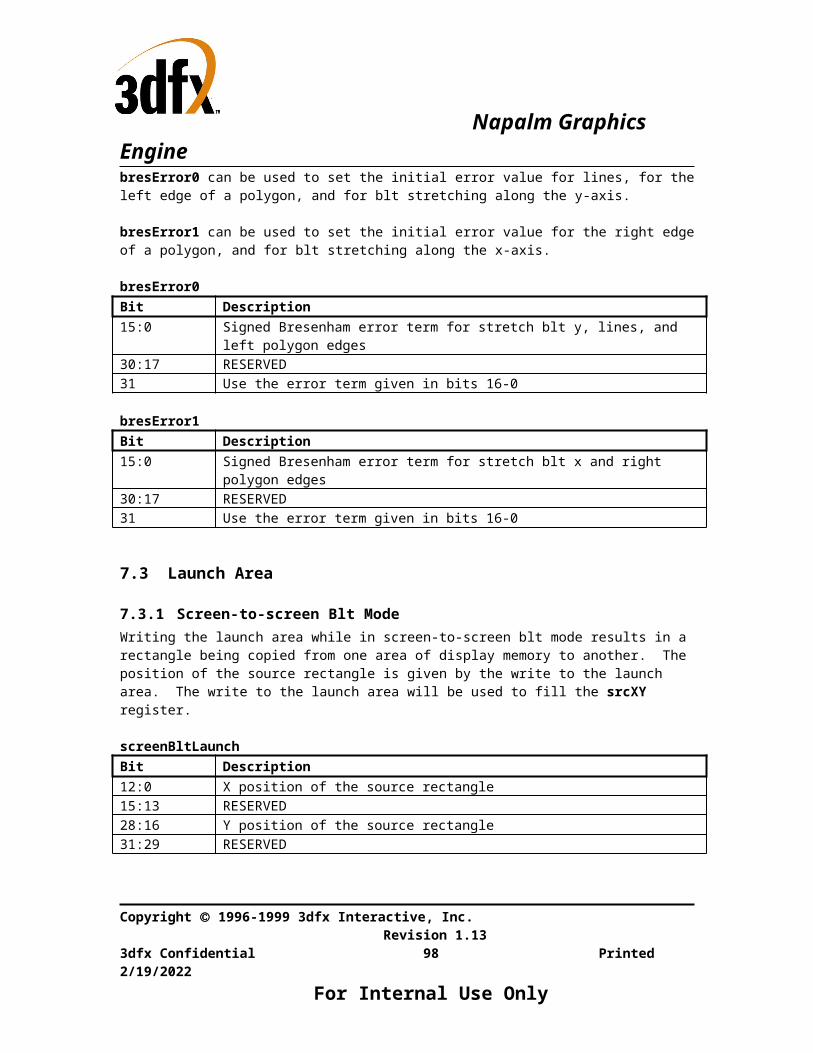
Napalm Graphics Engine
3=a_local, 4=texture alpha, 5=texture rgb, 6=zero, 7=c_mselect_7)13 Color Combine Unit control (cc_reverse_blend control)14 Color Combine Unit control (cc_add_clocal control)15 Color Combine Unit control (cc_add_alocal control)16 Color Combine Unit control (cc_invert_output control)17 Alpha Combine Unit control (cca_zero_other mux control: 0=a_other, 1=zero)18 Alpha Combine Unit control (cca_sub_clocal mux control: 0=zero, 1=a_local)21:19 Alpha Combine Unit control (cca_mselect mux control: 0=zero, 1=a_local, 2=a_other,
3=a_local, 4=texture alpha, 5=iterated alpha, 6=color1 alpha, 7=zero)22 Alpha Combine Unit control (cca_reverse_blend control)23 Alpha Combine Unit control (cca_add_clocal control)24 Alpha Combine Unit control (cca_add_alocal control)25 Alpha Combine Unit control (cca_invert_output control)26 Parameter Adjust (1=adjust parameters for subpixel correction)27 Enable Texture Mapping (1=enable)28 Enable RGBA, Z, and W parameter clamping (1=enable)29 Reserved31:30 Triangle iterators column band control (0=column-of-8, 1=column-of-16, 2=column-
of-32, 3=column-of-4)
Note that the color channels are controlled separately from the alpha channel. There are two primary color selection units: the Color Combine Unit(CCU) and the Alpha Combine Unit (ACU). Bits in fbzColorPath and combineMode control the Color Combine and Alpha Combine Units. combineMode bit(31) controls whether the controls for the “other,” “local,” and “mselect_7” MUX’s come from fbzColorPath or combineMode. See the combineMode register for more information. The diagram below illustrates the Color Combine Unit:
Copyright 1996-1999 3dfx Interactive, Inc. Revision 1.133dfx Confidential 98 Printed 5/7/2023
For Internal Use Only

Napalm Graphics Engine
Copyright 1996-1999 3dfx Interactive, Inc. Revision 1.133dfx Confidential 99 Printed 5/7/2023
For Internal Use Only

Napalm Graphics Engine The diagram below illustrates the Alpha Combine Unit:
Copyright 1996-1999 3dfx Interactive, Inc. Revision 1.133dfx Confidential 100 Printed 5/7/2023
For Internal Use Only
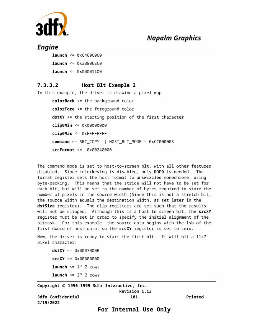
Napalm Graphics Engine
Bit(26) of fbzColorPath enables subpixel correction for all parameters. When enabled, Napalm will automatically subpixel correct the incoming color, depth, and texture coordinate parameters for triangles not aligned on integer spatial boundaries. Enabling subpixel correction decreases the on-chip triangle setup performance from 7 clocks to 16 clocks, but as the triangle setup engine is separately pipelined from the triangle rasterization engine, little if any performance penalty is seen when subpixel correction is enabled.
Important Note: When subpixel correction is enabled, the correction is performed on the start registers as they are passed into the triangle setup unit from the PCI FIFO. As a result, the host must pass down new starting parameter information for each new triangle -- if new starting parameter information is not passed down for a new triangle, the starting parameters will be subpixel corrected starting with the start registers already subpixel corrected for the last rendered triangle [in effect the parameters will be subpixel corrected twice, resulting in inaccuracies in the starting parameter values].
Bit(27) of fbzColorPath is used to enable texture mapping. If texture-mapped rendering is desired, then bit(27) of fbzColorPath must be set. When bit(27)=1, then data is transfered from TREX to FBI. If texture mapping is not desired (i.e. Gouraud shading, flat shading, etc.), then bit(27) may be cleared and no data is transfered from TREX to FBI.
Bit(28) of fbzColorpath is used to enable RGBA, Z, and W parameter clamping. When fbzColorpath bit(28)=1, then the RGBA triangle parameters are be clamped to [0,0xff] inclusive during triangle rasterization. Note that fbzColorpath bit(28) has no effect on the RGBA triangle parameters during triangle setup or sub-pixel correction. When fbzColorpath bit(28)=0, then the RGBA parameters are allowed to wrap according to the following formula:
if(rgbaIterator[23:12] == 0xfff)rgbaClamped[7:0] = 0x0;
else if(rgbaIterator[23:12] == 0x100)rgbaClamped[7:0] = 0xff;
elsergbaClamped[7:0] = rgbaIterator[19:12];
When fbzColorpath bit(28)=1, then the Z triangle parameter is clamped to [0,0xffff] inclusive during triangle rasterization. Note that fbzColorpath bit(28) has no effect on the Z triangle parameter during triangle setup or sub-pixel correction. Note also that the unclamped Z triangle iterator is used when performing floating point Z-buffering (fbzMode bit(21)=1). When fbzColorpath bit(28)=0, then the Z parameter is allowed to wrap according to the following formula:
if(zIterator[31:12] == 0xfffff)zClamped[15:0] = 0x0;
else if(zIterator[31:12] == 0x10000)zClamped[15:0] = 0xffff;
elsezClamped[15:0] = zIterator[27:12];
When fbzColorpath bit(28)=1, then the W triangle parameter is clamped to [0,0xff] inclusive for use in the Alpha Combine Unit and the fog unit. Note that fbzColorpath bit(28) has no effect on the W triangle parameter during triangle setup or sub-pixel correction. Note also that the unclamped W triangle iterator is used when performing floating point W-buffering (fbzMode bit(21)=0). When fbzColorpath
Copyright 1996-1999 3dfx Interactive, Inc. Revision 1.133dfx Confidential 101 Printed 5/7/2023
For Internal Use Only
Napalm Graphics Engine bit(28)=0, then the W parameter used as inputs to the ACU and fog units is allowed to wrap according to the following formula:
if(wIterator[47:32] == 0xffff)wClamped[7:0] = 0x0;
else if(zIterator[47:32] == 0x0100)wClamped[7:0] = 0xff;
elsewClamped[7:0] = wIterator[39:32];
fbzColorpath bits(31:30) control the column banding selection for the triangle iterators. FbzColorPath bits(31:30) can be changed to optimize performance for a given application.
8.21 combineMode RegisterThe combineMode register, along with the fbzColorPath and textureMode registers, controls the color and alpha rendering and texture pixel pipelines. Note that the chip field is used to direct writes to each individual combine unit.
Bit Description2:0 RGB-channel Combine Unit Control (cc_otherselect)5:3 RGB-channel Combine Unit Control (cc_localselect)8:6 RGB-channel Combine Unit Control (cc_mselect_7)10:9 RGB-channel Combine Unit Control (cc_invert_other)12:11 RGB-channel Combine Unit Control (cc_invert_local)13 RGB-channel Combine Unit Control (cc_invert_add_local)15:14 RGB-channel Combine Unit Control (cc_outshift) (0=no modulate, 1=modulate by 2,
2=modulate by 4, 3=reserved)17:16 Alpha-channel Combine Unit Control (cca_otherselect)20:18 Alpha-channel Combine Unit Control (cca_localselect)22:21 Alpha-channel Combine Unit Control (cca_invert_other)24:23 Alpha-channel Combine Unit Control (cca_invert_local)25 Alpha-channel Combine Unit Control (cca_invert_add_local)27:26 Alpha-channel Combine Unit Control (cca_outshift) (0=no modulate, 1=modulate by 2,
2=modulate by 4, 3=reserved)28 Reserved29 Enable 2 pixel-per-clock rendering operation (1=enable)30 Disable texture chroma substitution (1=use chromaRange register for constant colors
into the texture blending units)31 Color Combine Mode MUX selection control (0=use fbzColorPath, 1=use
combineMode)
The datapath control names (e.g. cc_otherselect, cca_localselect) are given for the Color Combine Unit and Alpha Combine Units. When the chip field directs a write to the combineMode register in a texture unit, the datapath controls are the texture datapath controls (e.g. tc_otherselect, tca_localselect).
When chromaRange[30:29]=0x3 and combineMode[30]=0, then texture chroma substitution is enabled. When combineMode[30]=1, then the chromaRange register is used to store constant color values in the texture units for texture blending. The chip fields are used to store different constant color values into each texture unit.
Copyright 1996-1999 3dfx Interactive, Inc. Revision 1.133dfx Confidential 102 Printed 5/7/2023
For Internal Use Only
Napalm Graphics Engine For the Color Combine and Alpha Combine Units (FBI combine units), combineMode bit(31) controls whether the controls for the “other,” “local,” and “mselect_7” MUX’s come from fbzColorPath or combineMode as follows:
MUX Control
CombineMode bit(31)=0 combineMode bit(31)=1
c_other {0, fbzColorPath[1:0]} combineMode[2:0]c_local {00, fbzColorPath[4]} combineMode[5:3]c_mselect_7 {000} combineMode[8:6]a_other fbzColorPath[3:2] combineMode[17:16]a_local {1’b0, fbzColorPath[6:5]} combineMode[20:18]
For the Texture Combine and Texture Alpha Combine units (in each TMU), the “other,” “local” and “mselect_7” (for the Texture Combine unit) always come from the combineMode register.
CombineMode bit(29) is used to enable 2 pixel-per-clock rendering. 2 pixel-per-clock rendering is only allowed to be enabled when a single texture is being applied per triangle. CombineMode bit(29) must be disabled when dual-texturing is being utilized. When 2 pixel-per-clock rendering is enabled (combineMode bit(29)=1), renderMode bits(24:22) contain the log2 of the number of scanlines rendered by each texture unit. RenderMode bits(24:22) can be changed to optimize performance for a given application. Also note that when 2 pixel-per-clock rendering is enabled, writes to either texture unit will be received by both. In other words, the ability to selectively write state and triangle information to individual texture units is disabled when 2 pixerl-per-clock rendering is enabled, as writes to either texture unit are received by both units. This functionality can be disabled by setting miscInit1[18].
*** Important Note: Due to a bug in the Napalm hardware, when switching from 2 pixel-per-clock rendering to single pixel-per-clock rendering, the TMU units must be idled. To accomplish this, send down at least 12 NOP commands with the chip field set to select both TMUs prior to the write to combineMode register clearing bit(29). This will flush the TMU pipelines (12 NOPs are necessary due to the pipelining between the FBI and TMU chips) before single pixel-per-clock rendering is selected by clearing combineMode bit(29). Note that the chip field for the NOP commands send to idle the TMUs should not select the FBI chip (i.e. set chipField=0x6), as this will cause the entire pixel pipeline to be flushed, resulting in unnecessary performance loss. Also note that sending 12 NOP commands prior to the combineMode write is not necessary when changing from single pixel-per-clock rendering mode to 2 pixel-per-clock rendering mode.
8.22 fogMode RegisterThe fogMode register is used to control the fog, alpha-blending, and dithering functionality of Napalm.
Bit Description0 Enable fog (1=enable)1 Fog Unit control (fogadd control: 0=fogColor, 1=zero)2 Fog Unit control (fogmult control: 0=Color Combine Unit RGB, 1=zero)3 Fog Unit control (fogalpha control)4 Fog Unit control (fogz control)5 Fog Unit control (fogconstant control: 0=fog multiplier output, 1=fogColor)6 Fog Unit control (fogdither control, dither the fog blending component)7 Fog Unit control (fogzones control, enable signed fog delta)8 RGB Channel alpha blending order of operations (0=[(S × ) alphaBlendOP (Dold × )],
Copyright 1996-1999 3dfx Interactive, Inc. Revision 1.133dfx Confidential 103 Printed 5/7/2023
For Internal Use Only
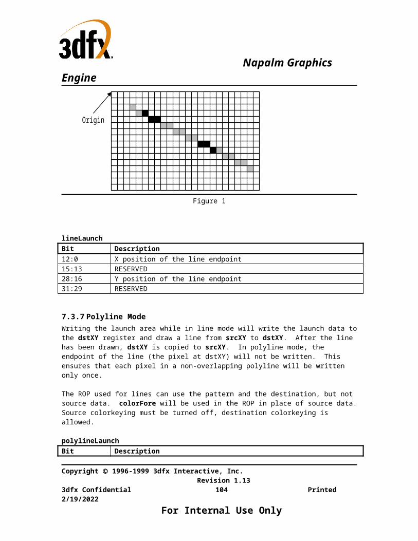
Napalm Graphics Engine
1=[(Dold × ) alphaBlendOP (S × )]9 RGB Channel alpha blending operation (alphaBlendOP) (0=add, 1=subtract)10 Alpha Channel alpha blending order of operations (0=[(S × ) alphaBlendOP (Dold × )],
1=[(Dold × ) alphaBlendOP (S × )]11 Alpha Channel alpha blending operation (alphaBlendOP) (0=add, 1=subtract)13:12 Rotated dither matrix select used for dither matrix calculations for triangle rendering15:14 Rotated dither matrix select used for dither matrix calculations for dither subtraction for
alpha-blended triangle rendering17:16 Rotated dither matrix select used for dither matrix calculations for rendering for triangles
repeated during AA rendering19:18 Rotated dither matrix select used for dither matrix calculations for dither subtraction (alpha-
blending logic) for triangles repeated during AA rendering31:20 reserved
The diagram below shows the fog unit of Napalm:
Copyright 1996-1999 3dfx Interactive, Inc. Revision 1.133dfx Confidential 104 Printed 5/7/2023
For Internal Use Only

Napalm Graphics Engine
Color Channel(from Color Combine Unit)
fogmult0 1
0
fogColor
fogadd0 1
0
9
2’s Comp
8
iterated w(4. 12 floating point)
64x8 RAM(fog alpha)
6 {4 bits exponent, mantissa(11:10)}
64x8 RAM(fog delta alpha)
6 {4 bits exponent, mantissa(11:10)}
8 (.8 format)
89 signed x 9 unsigned multiply
9
8
fogColor
Clamp FF
8 Fogged Color
fogenable
fogenable
1 0
1
mantissa(9:2)8
(6.2 format) 8
8 Color before fog
8 unsigned x 6 unsigned multiply
10 (6.4 format)
2’s Comp
11
10
fogzones 11
(6.0 format) 6
1 (0.1format,2nd lsb)
(7.0 format) 74 (0.4 format)
Dither Matrixbit(3)=y [0] xor x [0]bit(2)=y [0]bit(1)=y [1] xor x [1]bit(0)=y [1]
(0.4 format) 4
1 (carry-out)
fogdither
8
fog table alpha
iterated Z(27:20), clamped
0 21 3
iterated alpha
iterated W(39:32), clamped
{fogz, fogalpha}
fogconstant9 (1.8 format)
8 8
carry-in
Bit(0) of fogMode is used to enable fog and atmospheric effects. When fog is enabled, the fog color specified in the fogColor register is blended with the source pixels as a function of the fogTable values and iterated W. Napalm supports a 64-entry lookup table (fogTable) to support atmospheric effects such as fog and haze. When enabled, the MSBs of a normalized floating point representation of (1/W) is used to index into the 64-entry fog table. The ouput of the lookup table is an “alpha” value which represents the level of blending to be performed between the static fog/haze color and the incoming pixel color. 8 lower order bits of the floating point (1/W) are used to blend between multiple entries of the lookup table to reduce fog “banding.” The fog lookup table is loaded by the Host CPU, so various fog equations, colors, and effects can be supported.
Copyright 1996-1999 3dfx Interactive, Inc. Revision 1.133dfx Confidential 105 Printed 5/7/2023
For Internal Use Only

Napalm Graphics Engine The following table shows the mathematical equations for the supported values of bits(2:1) of fogMode when bits(5:3)=0:Bit(0) - EnableFog
Bit(1) - fogadd mux control
Bit(2) - fogmultmux control
Fog Equation
0 ignored ignored Cout = Cin1 0 0 Cout = Afog*Cfog + (1-Afog)*Cin1 0 1 Cout = Afog*Cfog1 1 0 Cout = (1-Afog)*Cin1 1 1 Cout = 0
where:Cout = Color output from Fog blockCin = Color input from Color Combine Unit ModuleCfog = fogColor registerAFog = alpha value calculated from Fog table
When bit(3) of fogMode is set, the integer part of the iterated alpha component is used as the fog alpha instead of the calculated fog alpha value from the fog table. When bit(4) of fogMode is set, the upper 8 bits of the iterated Z component are used as the fog alpha instead of the calculated fog alpha value from the fog table. If both bit(3) and bit(4) are set, then bit(4) takes precedence, and the upper 8 bits of the iterated Z component are used for the fog alpha value. Bit(5) of fogMode takes precedence over bits(4:3) and enables a constant value(fogColor) to be added to incoming source color.
fogMode bits(19:12) are used to rotate the matrix used for dithering calculations. fogMode bits(19:12) are only used if rotatation of the dither matrices is enabled (renderMode[25]=1). See the renderMode register description for more information on dither rotation.
8.23 alphaMode RegisterThe alphaMode register controls the alpha blending and anti-aliasing functionality of Napalm.
Bit Description0 Enable alpha function (1=enable)3:1 Alpha function (see table below)4 Enable alpha blending (1=enable)7:5 reserved11:8 Source RGB alpha blending factor (see table below)15:12 Destination RGB alpha blending factor (see table below)19:16 Source alpha-channel alpha blending factor (see table below)23:20 Destination alpha-channel alpha blending factor (see table below)31:24 Alpha reference value
Bits(3:1) specify the alpha function during rendering operations. The alpha function and test pipeline is shown below:
Copyright 1996-1999 3dfx Interactive, Inc. Revision 1.133dfx Confidential 106 Printed 5/7/2023
For Internal Use Only
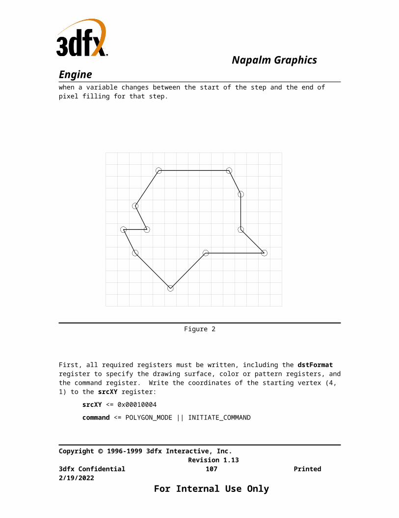
Napalm Graphics Engine
<? =?
1 1afunc_eqafunc_lt
afunc_gt
Alpha test pass
Alpha Testenable
Alpha from Alpha Combine Unit
alphaMode(31:24)
When alphaMode bit(0)=1, an alpha comparison is performed between the incoming source alpha and bits(31:24) of alphaMode. Section 5.18.1 below further describes the alpha function algorithm.
Bit(4) of alphaMode enables alpha blending. When alpha blending is enabled, the blending function is performed to combine the source color with the destination pixel. The blending factors of the source and destinations pixels are individually programmable, as determined by bits(23:8). Note that the RGB and alpha color channels may have different alpha blending factors. Section 5.18.2 below further describes alpha blending.
Bit(5) of alphaMode is reserved.
8.23.1 Alpha functionWhen the alpha function is enabled (alphaMode bit(0)=1), the following alpha comparison is performed:
AlphaSrc AlphaOP AlphaRefwhere AlphaSrc represents the alpha value of the incoming source pixel, and AlphaRef is the value of bits(31:24) of alphaMode. A source pixel is written into an RGB buffer if the alpha comparison is true and writing into the RGB buffer is enabled (fbzMode bit(9)=1. If the alpha function is enabled and the alpha comparison is false, the fbiAfuncFail register is incremented and the pixel is invalidated in the pixel pipeline and no drawing occurs to the alpha, color, depth, or stencil buffers. The supported alpha comparison functions (AlphaOPs) are shown below:
Value AlphaOP Function0 Never1 less than2 Equal
Copyright 1996-1999 3dfx Interactive, Inc. Revision 1.133dfx Confidential 107 Printed 5/7/2023
For Internal Use Only
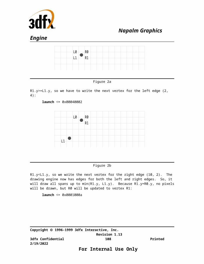
Napalm Graphics Engine 3 less than or equal4 greater than5 not equal6 greater than or equal7 Always
8.23.2 Alpha BlendingWhen alpha blending is enabled (alphaMode bit(4)=1), incoming source pixels are blended with destination pixels. The alpha blending function for the RGB color components are as follows:
Alpha Blending Order (fogMode[8])
Alpha Blending Operation (fogMode[9])
Calculated Alpha Blending Function
0 0 Dnew (S × ) + (Dold × )0 1 Dnew (S × ) - (Dold × )1 0 Dnew (Dold × ) + (S × )1 1 Dnew (Dold × ) - (S × )
whereDnew The new destination pixel being written into the frame bufferS The new source pixel being generatedDold The old (current) destination pixel about to be modified The source pixel alpha blending function. The destination pixel alpha blending function.
The alpha blending function for the alpha component is as follows:
Alpha Blending Order (fogMode[10])
Alpha Blending Operation (fogMode[11])
Calculated Alpha Blending Function
0 0 Anew (AS × d) + (Aold × d)0 1 Anew (AS × d) - (Aold × d)1 0 Anew (Aold × d) + (AS × d)1 1 Anew (Aold × d) - (AS × d)
whereAnew The new destination alpha being written into the alpha bufferAS The new source alpha being generatedAold The old (current) destination alpha about to be modifiedd The source alpha alpha-blending function. d The destination alpha alpha-blending function.
Note that the source and destination pixels may have different associated alpha blending functions. Also note that RGB color components and the alpha components may have different associated alpha blending functions. The alpha blending factors of the RGB color components are defined in bits(15:8) of alphaMode, while the alpha blending factors of the alpha component is specified in bits(23:16) of alphaMode. The following table lists the color channel alpha blending functions supported:
Alpha Blending Function Alpha Blending Function Pneumonic Alpha Blending Function Description0x0 AZERO Zero0x1 ASRC_ALPHA Source alpha0x2 A_COLOR Color
Copyright 1996-1999 3dfx Interactive, Inc. Revision 1.133dfx Confidential 108 Printed 5/7/2023
For Internal Use Only

Napalm Graphics Engine 0x3 ADST_ALPHA Destination alpha0x4 AONE One0x5 AOMSRC_ALPHA 1 - Source alpha0x6 AOM_COLOR 1 - Color0x7 AOMDST_ALPHA 1 - Destination alpha0x8 A_SAMECOLOR Same Color0x9 AOM_SAMECOLOR 1 – (Same Color)0xa-0xe Reserved0xf (source alpha blending function) ASATURATE MIN(Source alpha, 1 - Destination
alpha)0xf (destination alpha blending function) A_COLORBEFOREFOG Color before Fog Unit
When the value 0x2 is selected as the destination alpha blending factor (A_COLOR function), the source pixel color is used as the destination blending factor. When the value 0x2 is selected as the source alpha blending factor, the destination pixel color is used as the source blending factor. When the value 0x8 is selected as the destination alpha blending factor (A_SAMECOLOR function), the destination pixel color is used as the destination blending factor. When the value 0x8 is selected as the source alpha blending factor, the source pixel color is used as the source blending factor. Note also that the alpha blending function 0xf is different depending upon whether it is being used as a source or destination alpha blending function. When the value 0xf is selected as the destination alpha blending factor, the source color before the fog unit (“unfogged” color) is used as the destination blending factor -- this alpha blending function is useful for multi-pass rendering with atmospheric effects. When the value 0xf is selected as the source alpha blending factor, the alpha-saturate anti-aliasing algorithm is selected -- this MIN function performs polygonal anti-aliasing for polygons which are drawn front-to-back.
When running in 15BPP rendering mode (renderMode[1:0]=0x1) or 16BPP rendering mode (renderMode[1:0]=0x0), the following table lists the alpha channel alpha blending functions support (only relevant when the auxiliary buffer is setup to be an alpha buffer, fbzMode bit(18)=1):
15/16 BPP alpha channel alpha blending modesAlpha Blending Function Alpha Blending Function Pneumonic Alpha Blending Function Description0x0 AZERO Zero0x1-0x3 Reserved0x4 AONE One0x5-0xf Reserved
When running in 32 BPP rendering mode (renderMode[1:0]=0x2), the following table lists the 8-bit alpha channel alpha blending functions support:
32 BPP alpha channel alpha blending modesAlpha Blending Function Alpha Blending Function Pneumonic Alpha Blending Function Description0x0 AZERO Zero0x1 ASRC_ALPHA Source alpha0x2 Reserved0x3 ADST_ALPHA Destination alpha0x4 AONE One0x5 AOMSRC_ALPHA 1 - Source alpha0x6 Reserved0x7 AOMDST_ALPHA 1 - Destination alpha0x8-0xf Reserved
Copyright 1996-1999 3dfx Interactive, Inc. Revision 1.133dfx Confidential 109 Printed 5/7/2023
For Internal Use Only

Napalm Graphics Engine 8.24 lfbMode RegisterThe lfbMode register controls linear frame buffer accesses and queued VMI host port accesses.
Bit Description3:0 Linear frame buffer write format (see table below)5:4 Reserved7:6 Reserved8 Enable Napalm pixel pipeline-processed linear frame buffer writes (1=enable)10:9 Linear frame buffer RGBA lanes (see tables below)11 16-bit word swap linear frame buffer writes (1=enable)12 Byte swizzle linear frame buffer writes (1=enable)13 LFB access Y origin (0=top of screen is origin, 1=bottom of screen is origin)14 Linear frame buffer write access W select (0=LFB selected, 1=zacolor[23:0]).15 Reserved16 Reserved
The following table shows the supported Napalm linear frame buffer write formats:
Value Linear Frame Buffer Write Format16-bit formats
0 16-bit RGB (5-6-5)1 16-bit RGB (x-5-5-5)2 16-bit ARGB (1-5-5-5)3 Reserved
32-bit formats4 24-bit RGB (x-8-8-8)5 32-bit ARGB (8-8-8-8)7:6 Reserved8 32-bit depth9 Queued VMI host port write11:10 Reserved12 16-bit depth, 16-bit RGB (5-6-5)13 16-bit depth, 16-bit RGB (x-5-5-5)14 16-bit depth, 16-bit ARGB (1-5-5-5)15 16-bit depth, 16-bit depth When accessing the linear frame buffer, the cpu accesses information from the starting linear frame buffer (LFB) address space (see section 4 on Napalm address space) plus an offset which determines the <x,y> coordinates being accessed. Bits(3:0) of lfbMode define the format of linear frame buffer writes.
When writing to the linear frame buffer, lfbMode bit(8)=1 specifies that LFB pixels are processed by the normal Napalm pixel pipeline -- this implies each pixel written must have an associated depth and alpha value, and is also subject to the fog mode, alpha function, etc. If bit(8)=0, pixels written using LFB access bypass the normal Napalm pixel pipeline and are written to the specified buffer unconditionally and the values written are unconditionally written into the color/depth buffers except for optional color dithering [depth function, alpha blending, alpha test, and color/depth write masks are all bypassed when bit(8)=0]. If bit(8)=0, then only the buffers that are specified in the particular LFB format are updated. Also note that if lfbMode bit(8)=0 that the color and Z mask bits in fbzMode(bits 9 and 10) are ignored
Copyright 1996-1999 3dfx Interactive, Inc. Revision 1.133dfx Confidential 110 Printed 5/7/2023
For Internal Use Only

Napalm Graphics Engine for LFB writes. For example, if LFB modes 0-2, or 4 are used and bit(8)=0, then only the color buffers are updated for LFB writes (the depth buffer is unaffected by all LFB writes for these modes, regardless of the status of the Z-mask bit fbzMode bit 10). However, if LFB modes 12-14 are used and bit(8)=0, then both the color and depth buffers are updated with the LFB write data, irrespective of the color and Z mask bits in fbzMode. If LFB mode 15 is used and bit(8)=0, then only the depth buffer is updated for LFB writes (the color buffers are unaffected by all LFB writes in this mode, regardless of the status of the color mask bits in fbzMode).
If lfbMode bit(8)=0 and a LFB write format is selected which contains an alpha component (formats 2, 5, and 14) and the alpha buffer is enabled, then the alpha component is written into the alpha buffer. Conversely, if the alpha buffer is not enabled, then the alpha component of LFB writes using formats 2, 5, and 14 when bit(8)=0 are ignored. Note that anytime LFB formats 2, 5, and 14 are used when bit(8)=0 that blending and/or chroma-keying using the alpha component is not performed since the pixel-pipeline is bypassed when bit(8)=0.
If lfbMode bit(8)=0 and LFB write format 14 is used, the component that is ignored is determined by whether the alpha buffer is enabled -- If the alpha buffer is enabled and LFB write format 14 is used with bit(8)=0, then the depth component is ignored for all LFB writes. Conversely, if the alpha buffer is disabled and LFB write format is used with bit(8)=0, then the alpha component is ignored for all LFB writes.
If lfbMode bit(8)=1 and a LFB write access format does not include depth or alpha information (formats 0-5), then the appropriate depth and/or alpha information for each pixel written is taken from the zaColor register. Note that if bit(8)=1 that the LFB write pixels are processed by the normal Napalm pixel pipeline and thus are subject to the per-pixel operations including clipping, dithering, alpha-blending, alpha-testing, depth-testing, chroma-keying, fogging, and color/depth write masking.
Bits(10:9) of lfbMode specify the RGB channel format (color lanes) for linear frame buffer writes. The table below shows the Napalm supported RGB lanes:
Value RGB Channel Format0 ARGB1 ABGR2 RGBA3 BGRA
Bit(11) of lfbMode defines the format of 2 16-bit data types passed with a single 32-bit writes. For linear frame buffer formats 0-2, two 16-bit data transfers can be packed into one 32-bit write -- bit(11) defines which 16-bit shorts correspond to which pixels on screen. The table below shows the pixel packing for packed 32-bit linear frame buffer formats 0-2:
lfbMode bit(11) Screen Pixel Packing0 Right Pixel(host data 31:16), Left Pixel(host data 15:0)1 Left Pixel(host data 31:16), Right Pixel(host data 15:0)
For linear frame buffer formats 12-14, bit(11) of lfbMode defines the bit locations of the 2 16-bit data types passed. The table below shows the data packing for 32-bit linear frame buffer formats 12-14:
LfbMode bit(11)
Screen Pixel Packing
Copyright 1996-1999 3dfx Interactive, Inc. Revision 1.133dfx Confidential 111 Printed 5/7/2023
For Internal Use Only

Napalm Graphics Engine 0 Z value(host data 31:16), RGB value(host data 15:0)1 RGB value(host data 31:16), Z value(host data 15:0)
For linear frame buffer format 15, bit(11) of lfbMode defines the bit locations of the 2 16-bit depth values passed. The table below shows the data packing for 32-bit linear frame buffer format 15:
LfbMode bit(11)
Screen Pixel Packing
0 Z Right Pixel(host data 31:16), Z Left Pixel(host data 15:0)1 Z left Pixel(host data 31:16), Z Right Pixel(host data 15:0)
Note that bit(11) of lfbMode is ignored for linear frame buffer writes using formats 4 , 5 or 8.
Bit(12) of lfbMode is used to enable byte swizzling. When byte swizzling is enabled, the 4-bytes within a 32-bit word are swizzled to correct for endian differences between Napalm and the host CPU. For little endian CPUs (e.g. Intel x86 processors) byte swizzling should not be enabled, however big endian CPUs (e.g. PowerPC processors) should enable byte swizzling. For linear frame buffer writes, the bytes within a word are swizzled prior to being modified by the other control bits of lfbMode. When byte swizzling is enabled, bits(31:24) are swapped with bits(7:0), and bits(23:16) are swapped with bits(15:8).
Very Important Note: The order of swapping and swizzling operations for LFB writes is as follows: byte swizzling is performed first on all incoming LFB data, as defined by lfbMode bit(12) and irrespective of the LFB data format. After byte swizzling, 16-bit word swapping is performed as defined by lfbMode bit(11). Note that 16-bit word swapping is never performed on LFB data when data formats 4 and 5 are used. Also note that 16-bit word swapping is performed on the LFB data that was previously optionally swapped. Finally, after both swizzling and 16-bit word swapping are performed, the individual color channels are selected as defined in lfbMode bits(10:9). Note that the color channels are selected on the LFB data that was previously swizzled and/or swapped
Bit(13) of lfbMode is used to define the origin of the Y coordinate for all linear frame buffer writes when the pixel pipeline is bypassed (lfbMode bit(8)=0). Note that bit(13) of lfbMode does not affect rendering operations (FASTFILL and TRIANGLE commands) -- bit(17) of fbzMode defines the origin of the Y coordinate for rendering operations. Note also that if the pixel pipeline is enabled for linear frame buffer writes (lfbMode bit(8)=1), then fbzMode bit(17) is used to determine the location of the Y origin. When cleared, the Y origin (Y=0) for all linear frame buffer accesses is defined to be at the top of the screen. When bit(13) is set, the Y origin for all linear frame buffer accesses is defined to be at the bottom of the screen.
Bit(14) of lfbMode is used to select the W component used for LFB writes processed through the pixel pipeline. If bit(14)=0, then the MSBs of the fractional component of the 48-bit W value passed to the pixel pipeline for LFB writes through the pixel pipeline is the Z value associated with the LFB write. [Note that the Z value associated with the LFB write is dependent on the LFB format, and is either passed down pixel-by-pixel from the CPU, or is set to the constant zaColor]. If bit(14)=1, then the MSBs of the fractional component of the 48-bit W value passed to the pixel pipeline for LFB writes is zacolor(23:0). Regardless of the setting of bit(14), when LFB writes go through the pixel pipeline, all other bits except the 16 MSBs of the fractional component of the W value are set to 0x0. Note that bit(14) is ignored if LFB writes bypass the pixel pipeline.
8.24.1 Linear Frame Buffer Writes
Linear frame buffer writes -- format 0:Copyright 1996-1999 3dfx Interactive, Inc. Revision 1.133dfx Confidential 112 Printed 5/7/2023
For Internal Use Only

Napalm Graphics Engine When writing to the linear frame buffer with 16-bit format 0 (RGB 5-6-5), the RGB channel format specifies the RGB ordering within a 16-bit word. If the Napalm pixel pipeline is enabled for LFB accesses (lfbMode bit(8)=1), then alpha and depth information for LFB format 0 is taken from the zaColor register. When running in 15BPP rendering mode and the pixel pipeline is bypassed, then the stored 1-bit alpha is determined as follows: if renderMode[16:15]=0, then the 1-bit alpha is 0; if renderMode[16:15]=1, then the 1-bit alpha is 1; otherwise, if renderMode[16:15]=2, then the 1-bit alpha is taken from zaColor[31]. The following table shows the color channels for 16-bit linear frame buffer access format 0:
RGB Channel Format Value
16-bit Linear frame buffer access bits
RGB Channel
0 15:0 Red (15:11), Green(10:5), Blue(4:0)1 15:0 Blue (15:11), Green(10:5), Red(4:0)2 15:0 Red (15:11), Green(10:5), Blue(4:0)3 15:0 Blue (15:11), Green(10:5), Red(4:0)
Linear frame buffer writes -- format 1:When writing to the linear frame buffer with 16-bit format 1 (RGB 5-5-5), the RGB channel format specifies the RGB ordering within a 16-bit word. If the Napalm pixel pipeline is enabled for LFB accesses (lfbMode bit(8)=1), then alpha and depth information for LFB format 1 is taken from the zaColor register. When running in 15BPP rendering mode and the pixel pipeline is bypassed, then the stored 1-bit alpha is determined as follows: if renderMode[16:15]=0, then the 1-bit alpha is 0; if renderMode[16:15]=1, then the 1-bit alpha is 1; otherwise, if renderMode[16:15]=2, then the 1-bit alpha is taken from zaColor[31]. The following table shows the color channels for 16-bit linear frame buffer access format 1:
RGB Channel Format Value
16-bit Linear frame buffer access bits
RGB Channel
0 15:0 Ignored(15), Red (14:10), Green(9:5), Blue(4:0)1 15:0 Ignored(15), Blue (14:10), Green(9:5), Red(4:0)2 15:0 Red (15:11), Green(10:6), Blue(5:1), Ignored(0)3 15:0 Blue (15:11), Green(10:6), Red(5:1), Ignored(0)
Linear frame buffer writes -- format 2:When writing to the linear frame buffer with 16-bit format 2 (ARGB 1-5-5-5), the RGB channel format specifies the RGB ordering within a 16-bit word. If the Napalm pixel pipeline is enabled for LFB accesses (lfbMode bit(8)=1), then depth information for LFB format 2 is taken from the zaColor register. Note that the 1-bit alpha value passed when using LFB format 2 is bit-replicated to yield the 8-bit alpha used in the pixel pipeline. The following table shows the color channels for 16-bit linear frame buffer access format 2:
RGB Channel Format Value
16-bit Linear frame buffer access bits
RGB Channel
0 15:0 Alpha(15), Red (14:10), Green(9:5), Blue(4:0)1 15:0 Alpha(15), Blue (14:10), Green(9:5), Red(4:0)2 15:0 Red (15:11), Green(10:6), Blue(5:1), Alpha(0)3 15:0 Blue (15:11), Green(10:6), Red(5:1), Alpha(0)
Linear frame buffer writes -- format 3:Linear frame buffer format 3 is an unsupported format.
Copyright 1996-1999 3dfx Interactive, Inc. Revision 1.133dfx Confidential 113 Printed 5/7/2023
For Internal Use Only
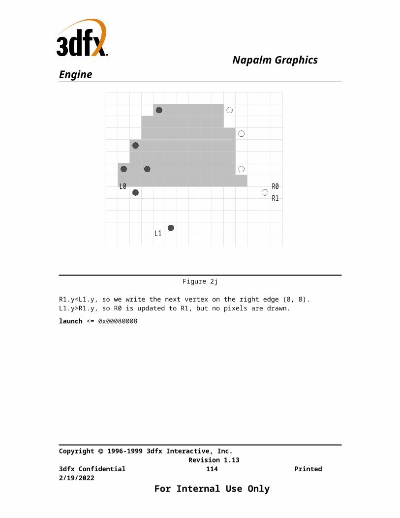
Napalm Graphics Engine
Linear frame buffer writes -- format 4:When writing to the linear frame buffer with 24-bit format 4 (RGB x-8-8-8), the RGB channel format specifies the RGB ordering within a 24-bit word. Note that the alpha/A channel is ignored for 24-bit access format 4. Also note that while only 24-bits of data is transfered for format 4, all data access must be 32-bit aligned -- packed 24-bit writes are not supported by Napalm. If the Napalm pixel pipeline is enabled for LFB accesses (lfbMode bit(8)=1), then alpha and depth information for LFB format 4 is taken from the zaColor register. When running in 15BPP rendering mode and the pixel pipeline is bypassed, then the stored 1-bit alpha is determined as follows: if renderMode[16:15]=0, then the 1-bit alpha is 0; if renderMode[16:15]=1, then the 1-bit alpha is 1; otherwise, if renderMode[16:15]=2, then the 1-bit alpha is taken from zaColor[31]. The following table shows the color channels for 24-bit linear frame buffer access format 4:
RGB Channel Format Value
24-bit Linear frame buffer access bits
(aligned to 32-bits)
RGB Channel
0 31:0 Ignored(31:24), Red (23:16), Green(15:8), Blue(7:0)1 31:0 Ignored(31:24), Blue(23:16), Green(15:8), Red(7:0)2 31:0 Red(31:24), Green(23:16), Blue(15:8), Ignored(7:0)3 31:0 Blue(31:24), Green(23:16), Red(15:8), Ignored(7:0)
Linear frame buffer writes -- format 5:When writing to the linear frame buffer with 32-bit format 5 (ARGB 8-8-8-8), the RGB channel format specifies the ARGB ordering within a 32-bit word. If the Napalm pixel pipeline is enabled for LFB accesses (lfbMode bit(8)=1), then depth information for LFB format 5 is taken from the zaColor register. The following table shows the color channels for 32-bit linear frame buffer access format 5.
RGB Channel Format Value
24-bit Linear frame buffer access bits
(aligned to 32-bits)
RGB Channel
0 31:0 Alpha(31:24), Red (23:16), Green(15:8), Blue(7:0)1 31:0 Alpha(31:24), Blue(23:16), Green(15:8), Red(7:0)2 31:0 Red(31:24), Green(23:16), Blue(15:8), Alpha(7:0)3 31:0 Blue(31:24), Green(23:16), Red(15:8), Alpha(7:0)
Linear frame buffer writes -- formats 6-7:Linear frame buffer formats 6-7 are unsupported formats.
Linear frame buffer writes -- format 8:When writing to the linear frame buffer with 32-bit format 8 (Depth 32), the format of the depth values passed must precisely match the format of the type of depth buffering being used (either integer Z or floating point 1/W). If the Napalm pixel pipeline is enabled for LFB accesses (lfbMode bit(8)=1), then RGB color information is taken from the color1 register, and alpha information for LFB format 15 is taken from the zaColor register.
When running in 32BPP rendering mode (renderMode[1:0]=0x2) and the pixel pipeline is bypassed, incoming data bits(31:8) [after byte swizzling] are stored in the 24-bit depth buffer. When running in 32BPP rendering mode and the pixel pipeline is enabled, then incoming data bits(31:8) are used as the 24-bit integer Z value for the pixel pipeline, and incoming data bits(7:0) are used as the msb of the fractional component of the Z value for the pixel pipeline.
Copyright 1996-1999 3dfx Interactive, Inc. Revision 1.133dfx Confidential 114 Printed 5/7/2023
For Internal Use Only

Napalm Graphics Engine When running in 15 or 16BPP rendering mode and the pixel pipeline is bypassed, incoming bits (31:16) [after byte swizzling] are stored in the 16-bit depth buffer. When running in 15 or 16 BPP rendering mode and the pixel pipeline is enabled, then incoming data bits(31:8) are used as the 24-bit integer Z value for the pixel pipeline, and incoming data bits(7:0) are used as the msb of the fractional component of the Z value for the pixel pipeline.
Linear frame buffer writes -- format 9:See below for a description of format 9, which is used for queued VMI host port accesses.
Linear frame buffer writes -- formats 10-11:Linear frame buffer formats 10-11 are unsupported formats.
Linear frame buffer writes -- format 12:When writing to the linear frame buffer with 32-bit format 12 (Depth 16, RGB 5-6-5), the RGB channel format specifies the RGB ordering within the 32-bit word. If the Napalm pixel pipeline is enabled for LFB accesses (lfbMode bit(8)=1), then alpha information for LFB format 12 is taken from the zaColor register. When running in 15BPP rendering mode and the pixel pipeline is bypassed, then the stored 1-bit alpha is determined as follows: if renderMode[16:15]=0, then the 1-bit alpha is 0; if renderMode[16:15]=1, then the 1-bit alpha is 1; otherwise, if renderMode[16:15]=2, then the 1-bit alpha is taken from zaColor[31]. Note that the format of the depth value passed when using LFB format 12 must precisely match the format of the type of depth buffering being used (either 16-bit integer Z or 16-bit floating point 1/W). The following table shows the 16-bit color channels within the 32-bit linear frame buffer access format 12:
RGB Channel Format Value
16-bit Linear frame buffer access bits
RGB Channel
0 15:0 Red (15:11), Green(10:5), Blue(4:0)1 15:0 Blue (15:11), Green(10:5), Red(4:0)2 15:0 Red (15:11), Green(10:5), Blue(4:0)3 15:0 Blue (15:11), Green(10:5), Red(4:0)When running in 32BPP rendering mode, the 16-bit incoming depth value is converted to a 24-bit depth value by taking the 8 most-significant-bits of the 16-bit incoming depth value and placing them to the right of the 16-bit incoming depth value to form a 24-bit word (this is otherwise known as MSB bit replication).
Linear frame buffer writes -- format 13:When writing to the linear frame buffer with 32-bit format 13 (Depth 16, RGB x-5-5-5), the RGB channel format specifies the RGB ordering within the 32-bit word. If the Napalm pixel pipeline is enabled for LFB accesses (lfbMode bit(8)=1), then alpha information for LFB format 13 is taken from the zaColor register. When running in 15BPP rendering mode and the pixel pipeline is bypassed, then the stored 1-bit alpha is determined as follows: if renderMode[16:15]=0, then the 1-bit alpha is 0; if renderMode[16:15]=1, then the 1-bit alpha is 1; otherwise, if renderMode[16:15]=2, then the 1-bit alpha is taken from zaColor[31]. Note that the format of the depth value passed when using LFB format 13 must precisely match the format of the type of depth buffering being used (either 16-bit integer Z or 16-bit floating point 1/W). The following table shows the 16-bit color channels within the 32-bit linear frame buffer access format 13:
RGB Channel Format Value
16-bit Linear frame buffer access bits
RGB Channel
0 15:0 Ignored(15), Red (14:10), Green(9:5), Blue(4:0)1 15:0 Ignored(15), Blue (14:10), Green(9:5), Red(4:0)
Copyright 1996-1999 3dfx Interactive, Inc. Revision 1.133dfx Confidential 115 Printed 5/7/2023
For Internal Use Only

Napalm Graphics Engine 2 15:0 Red (15:11), Green(10:6), Blue(5:1), Ignored(0)3 15:0 Blue (15:11), Green(10:6), Red(5:1), Ignored(0)When running in 32BPP rendering mode, the incoming 16-bit depth values are converted to the 24-bit depth required by the method described in the description of linear frame buffer write format 12.
Linear frame buffer writes -- format 14:When writing to the linear frame buffer with 32-bit format 14 (Depth 16, ARGB 1-5-5-5), the RGB channel format specifies the RGB ordering within the 32-bit word. Note that the format of the depth value passed when using LFB format 14 must precisely match the format of the type of depth buffering being used (either 16-bit integer Z or 16-bit floating point 1/W). Also note that the 1-bit alpha value passed when using LFB format 14 is bit-replicated to yield the 8-bit alpha used in the pixel pipeline. The following table shows the 16-bit color channels within the 32-bit linear frame buffer access format 14:
RGB Channel Format Value
16-bit Linear frame buffer access bits
RGB Channel
0 15:0 Alpha(15), Red (14:10), Green(9:5), Blue(4:0)1 15:0 Alpha(15), Blue (14:10), Green(9:5), Red(4:0)2 15:0 Red (15:11), Green(10:6), Blue(5:1), Alpha(0)3 15:0 Blue (15:11), Green(10:6), Red(5:1), Alpha(0)When running in 32BPP rendering mode, the incoming 16-bit depth values are converted to the 24-bit depth required by the method described in the description of linear frame buffer write format 12.
Linear frame buffer writes -- format 15:When writing to the linear frame buffer with 32-bit format 15 (Depth 16, Depth 16), the format of the depth values passed must precisely match the format of the type of depth buffering being used (either 16-bit integer Z or 16-bit floating point 1/W). If the Napalm pixel pipeline is enabled for LFB accesses (lfbMode bit(8)=1), then RGB color information is taken from the color1 register, and alpha information for LFB format 15 is taken from the zaColor register. When running in 32BPP rendering mode, the incoming 16-bit depth values are converted to the 24-bit depth required by the method described in the description of linear frame buffer write format 12.
Queued VMI host port writes -- format 9:When writing to the linear frame buffer with format 9, no data is written to the frame buffer or passed down the 3D pipeline. Instead, writes are performed to the VMI host port. When lfb write format 9 is specified, all other bits in lfbMode are ignored. For lfb writes of lfb format 9, each 32-bit word that is transferred holds both the 8-bit data that is to be written to the VMI host port, and also some control and address information. The 32-bit word written for lfb write format 9 is as follows:
Bit Description7:0 VMI host port data11:8 VMI host port address12 VMI host port control signal vmi_rw value13 VMI host port control signal vmi_cs_n value14 VMI host port write mode (0=mode A, 1=mode B)15 VMI host port access speed (0=normal, 1=1/2 speed)16 Execute VMI host port writes (1=execute write)31:17 Reserved
When a write to the 3D linear frame buffer space is received and lfbMode bits(3:0)=0x9, then the address of the 3D lfb is ignored and the 32-bit data which is written is used to control the queued VMI
Copyright 1996-1999 3dfx Interactive, Inc. Revision 1.133dfx Confidential 116 Printed 5/7/2023
For Internal Use Only
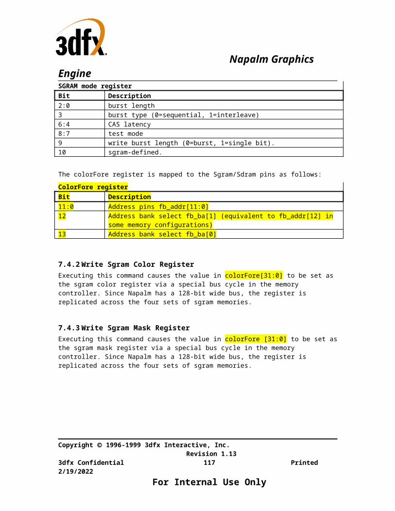
Napalm Graphics Engine host port write. The address and data information for the VMI host port write are stored in the data word bits(11:0). Bit(12) of the data word is used to control the vmi_rw signal - this value will typically be 0 for active low write enables (the standard configuration for VMI). Similarly, bit(13) of the data word is used to control the vmi_cs_n signal - again, this value is typically 0 for standard VMI implementations.
Bit(14) of the data word is used to specify which access mode, either Mode A or Mode B (see the VMI specification for a description of these two host port access modes) the queued VMI host port write uses. Whether to use Mode A or Mode B is implementation specific. Bit(15) of the data word is used to control the access speed of the VMI host port write state machine. Setting bit(15)=1 will slow down all timing used by the state machine by ½ normal speed. Bit(15) should not have to be used for normal operation, but is included in case some VMI device is found that does not conform to VMI host port timing specifications.
When bit(16) of the data word is set, then a queued VMI host port write occurs. If bit(16) of the data word is not set, then the values of the VMI host port address, data, vmi_rw, and vmi_cs_n are set to the values specified in the data word bits(13:0), but no VMI host port write is generated.
*** Note that for queued VMI host port writes to be enabled, miscInit0 bit(31) must be set. Setting miscInit0 bit(31) causes the VMI host port signals to be controlled by the queued VMI host port write mechanism in the 3D lfb write logic as described above. When miscInit0 bit(31) is cleared, then the VMI host port signals are controlled by the vidSerialParallelPort register and 3D lfb writes with format 9 will not generate VMI host port accesses.
8.25 fbzMode RegisterThe fbzMode register controls frame buffer and depth buffer rendering functions of the Napalm processor. Bits in fbzMode control clipping, chroma-keying, depth-buffering, dithering, and masking.
Bit Description0 Enable clipping rectangle (1=enable)1 Enable chroma-keying (1=enable)2 Enable stipple register masking (1=enable)3 W-Buffer Select (0=Use Z-value for depth buffering, 1=Use W-value for depth
buffering)4 Enable depth-buffering (1=enable)7:5 Depth-buffer function (see table below)8 Enable dithering (1=enable)9 RGB buffer write mask (0=disable writes to RGB buffer)10 Depth/alpha buffer write mask (0=disable writes to depth/alpha buffer)11 Dither algorithm (0=4x4 ordered dither, 1=2x2 ordered dither)12 Enable Stipple pattern masking (1=enable)13 Enable Alpha-channel mask (1=enable alpha-channel masking)15:14 Reserved16 Enable depth-biasing (1=enable)17 Rendering commands Y origin (0=top of screen is origin, 1=bottom of screen is origin)18 Enable alpha planes (1=enable)19 Enable alpha-blending dither subtraction (1=enable)20 Depth buffer source compare select (0=normal operation, 1=zaColor)21 Depth float select (0=iterated W is used for floating point depth buffering, 1=iterated Z
is used for floating point depth buffering)
Copyright 1996-1999 3dfx Interactive, Inc. Revision 1.133dfx Confidential 117 Printed 5/7/2023
For Internal Use Only

Napalm Graphics Engine
Bit(0) of fbzMode is used to enable the clipping register. When set, clipping to the rectangle defined by the clipLeftRight and clipBottomTop registers inclusive is enabled. When clipping is enabled, the bounding clipping rectangle must always be less than or equal to the screen resolution in order to clip to screen coordinates. Also note that if clipping is not enabled, rendering may not occur outside of the screen resolution. Bit(1) of fbzMode is used to enable the color compare check (chroma-keying). When enabled, any source pixel matching the color specified in the chromaKey register is not written to the RGB buffer. The chroma-key color compare is performed immediately after texture mapping lookup, but before the color combine unit and fog in the pixel datapath.
Bit(2) of fbzMode is used to enable stipple register masking. When enabled, bit(12) of fbzMode is used to determine the stipple mode -- bit(12)=0 specifies stipple rotate mode, while bit(12)=1 specifies stipple pattern mode.
When stipple register masking is enabled and stipple rotate mode is selected, bit(31) of the stipple register is used to mask pixels in the pixel pipeline. For all triangle commands and linear frame buffer writes through the pixel pipeline, pixels are invalidated in the pixel pipeline if stipple bit(31)=0 and stipple register masking is enabled in stipple rotate mode. After an individual pixel is processed in the pixel pipeline, the stipple register is rotated from right-to-left, with the value of bit(0) filled with the value of bit(31). Note that the stipple register is rotated regardless of whether stipple masking is enabled (bit(2) in fbzMode) when in stipple rotate mode.
When stipple register masking is enabled and stipple pattern mode is selected, the spatial <x,y> coordinates of a pixel processed in the pixel pipeline are used to lookup a 4x8 monochrone pattern stored in the stipple register -- the resultant lookup value is used to mask pixels in the pixel pipeline. For all triangle commands and linear frame buffer writes through the pixel pipeline, a stipple bit is selected from the stipple register as follows:
switch(pixel_Y[1:0]) {case 0: stipple_Y_sel[7:0] = stipple[7:0];
case 1: stipple_Y_sel[7:0] = stipple[15:8];case 2: stipple_Y_sel[7:0] = stipple[23:16];case 3: stipple_Y_sel[7:0] = stipple[31:24];
}switch(pixel_X[2:0] {
case 0: stipple_mask_bit = stipple_Y_sel[7];case 1: stipple_mask_bit = stipple_Y_sel[6];case 2: stipple_mask_bit = stipple_Y_sel[5];case 3: stipple_mask_bit = stipple_Y_sel[4];case 4: stipple_mask_bit = stipple_Y_sel[3];case 5: stipple_mask_bit = stipple_Y_sel[2];case 6: stipple_mask_bit = stipple_Y_sel[1];case 7: stipple_mask_bit = stipple_Y_sel[0];
}If the stipple_mask_bit=0, the pixel is invalidated in the pixel pipeline when stipple register masking is enabled and stipple pattern mode is selected. Note that when stipple pattern mode is selected the stipple register is never rotated.
Bits(4:3) specify the depth-buffering function during rendering operations. The depth buffering pipeline is shown below:
Copyright 1996-1999 3dfx Interactive, Inc. Revision 1.133dfx Confidential 118 Printed 5/7/2023
For Internal Use Only

Napalm Graphics Engine
iterated W[47:0], unclamped
wfloat_select1 0
16
iterated Z[27:12], clamped
48 floatSel
16
16 (integer only)
Clamp
zaColor[15:0]zbias_enable
16
<? =?
1 1
old Depth(from Depth Buffer)
zfunc_eqzfunc_lt
zfunc_gt
Depth test pass
Depth Bufferenable
cin wfloat_select1. Sign extend 16-bit zaColor to 18 bits2. Convert 16-bit depth to 18-bit {underflow,underflow,depth}3. Add 18-bit values4. Clamp to 0-FFFF
wfloat format: 1.<mant> * 2^exp
Clamp
cin = 1
To Fog Unit
4 12
12 mantissaexponent 4
if(|floatSel[47:32]) { mant = 0, exp = 0xf, underflow = 1} else if(!| floatSel[31:16]) { mant = 1, exp = 0xf, underflow = 0} else { exp = find_first_one(floatSel[31:16]) mant = (floatSel[30:16] << exp), underflow = 0}
underflow 1
To adder logic
depthfloat_select1 0
iterated Z[31:0], unclamped
if(|w-iter[47:32]) { mant = 0, exp = 0xf, underflow = 1} else if(!| w-iter[31:16]) { mant = 1, exp = 0xf, underflow = 0} else { exp = find_first_one(w=iter[31:16]) mant = (w-iter[30:16] << exp), underflow = 0}
iterated W[47:0], unclamped
48
4 12
12 mantissaexponent 4
16
treat as 4.28 value, line up decimal points with 16.32 w-term and zero extended to 48 bits
Bit(4) of fbzMode is used to enable depth-buffering. When depth buffering is enabled, a depth comparison is performed for each source pixel as defined in bits(7:5). When bit(3)=0, the z iterator is Copyright 1996-1999 3dfx Interactive, Inc. Revision 1.133dfx Confidential 119 Printed 5/7/2023
For Internal Use Only

Napalm Graphics Engine used for the depth buffer comparison. When bit(3)=1, the w iterator is used for the depth buffer comparison. When bit(3)=1 enabling w-buffering, the inverse of the normalized w iterator is used for the depth-buffer comparison. This in effect implements a floating-point w-buffering scheme utilizing a 4-bit exponent and a 12-bit mantissa. The inverted w iterator is used so that the same depth buffer comparisons can be used as with a typical z-buffer. Section 5.19.1 below further describes the depth-buffering algorithm.
Bit(8) of fbzMode enables 16-bit color dithering. When enabled, native 24-bit source pixels are dithered into 16-bit RGB color values with no performance penalty. When dithering is disabled, native 24-bit source pixels are converted into 16-bit RGB color values by bit truncation. When dithering is enabled, bit(11) of fbzMode defines the dithering algorithm -- when bit(11)=0 a 4x4 ordered dither algorithm is used, and when bit(11)=1 a 2x2 ordered dither algorithm is used to convert 24-bit RGB pixels into 16-bit frame buffer colors. fbzMode bit(8) must be cleared when 32-bit color rendering is selected (renderMode[1:0]=0x2).
Bit(9) of fbzMode enables writes to the RGB buffers. Clearing bit(9) invalidates all writes to the RGB buffers, and thus the RGB buffers remain unmodified for all rendering operations. Bit(9) must be set for normal drawing into the RGB buffers. Note that when running in 15 BPP rendering mode (renderMode[1:0]=0x1), fbzMode bit(9) controls writes to the 1-bit alpha plane in addition to controlling writes to the RGB color planes. There is no capability when running in 15 BPP rendering mode to selectively disable writes to only the RGB or the alpha planes – both the RGB planes and the 1-bit alpha plane are controlled together by fbzMode bit(9). Note that when running in 32 BPP rendering mode, fbzMode bit(9) must be set to enable writes to any of the color planes -- writes to the individual color planes are then controlled by renderMode bits(19:17). Also note in 32 BPP rendering mode that clearing fbzMode bit(9) causes all color planes to not be written, regardless of the individual settings of renderMode bits(19:17).
Bit(10) enables writes to the depth-buffer/alpha buffer. When cleared, writes to the depth-buffer are invalidated, and the depth-buffer state is unmodified for all rendering operations. Bit(10) must be set for normal depth-buffered operation. Note that when running in 15 BPP rendering mode, the auxiliary buffer must be setup as a depth buffer (fbzMode bit(18)=0) and thus fbzMode bit(10) is used to enable writes to the depth buffer – fbzMode bit(9) is then used to enable writes to the 1-bit alpha plane. Note that when running in 32 BPP rendering mode, fbzMode bit(10) enables writes to the depth-buffer, while renderMode bit(20) enables writes to the destination alpha-buffer.
Bit(13) of fbzMode enables the alpha-channel mask. When enabled, bit(0) of the incoming alpha value is used to mask writes to the color and depth buffers. If alpha channel masking is enabled and bit(0) of the incoming alpha value is 0, then the pixel is invalidated in the pixel pipeline, the fbiAfuncFail register is incremented, and no drawing occurs to the color or depth buffers. If alpha channel masking is enabled and bit(0) of the incoming alpha value is 1, then the pixel is drawn normally subject to depth function, alpha blending function, alpha test, and color/depth masking.
Bit(16) of fbzMode is used to enable the Depth Buffer bias. When bit(16)=1, the calculated depth value (irrespective of Z or 1/W type of depth buffering selected) is added to the depth field of zaColor. Depth buffer biasing is used to elimate aliasing artifacts when rendering co-planar polygons.
Bit(17) of fbzMode is used to define the origin of the Y coordinate for rendering operations (FASTFILL and TRIANGLE commands) and linear frame buffer writes when the pixel pipeline is bypassed for linear frame buffer writes (lfbMode bit(8)=0). Note that bit(17) of fbzMode does not affect linear frame buffer writes when the pixel pipeline is bypassed for linear frame buffer writes (lfbMode bit(8)=0), as in this situation bit(13) of lfbMode specifies the Y origin for linear frame buffer writes. When cleared, the Y origin (Y=0) for all rendering operations and linear frame buffer writes when the pixel pipeline is enabled
Copyright 1996-1999 3dfx Interactive, Inc. Revision 1.133dfx Confidential 120 Printed 5/7/2023
For Internal Use Only
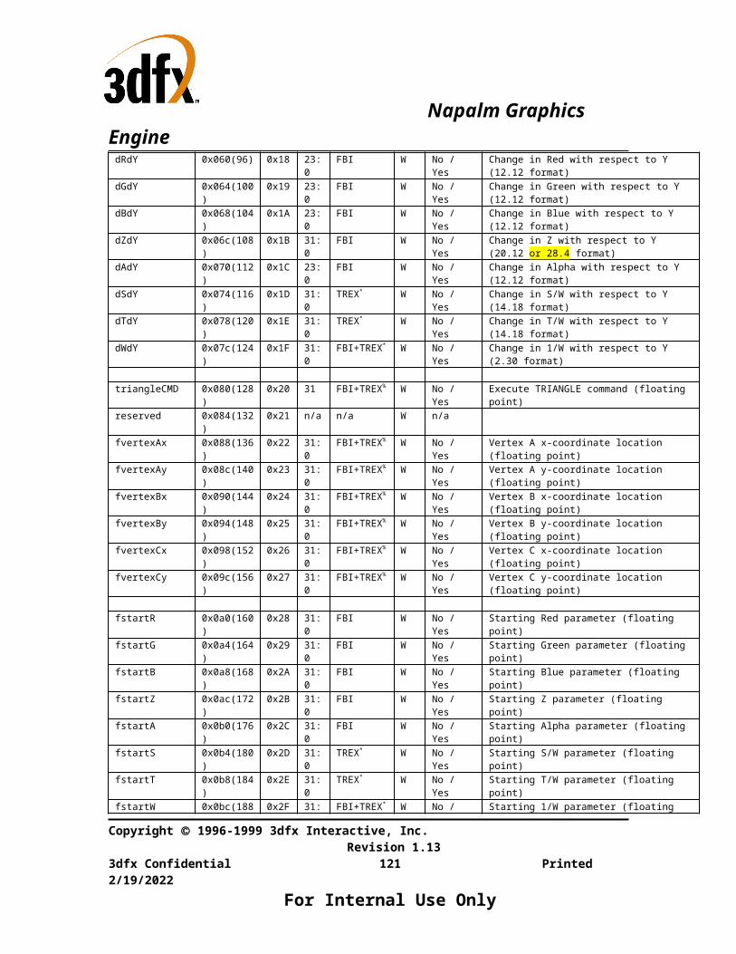
Napalm Graphics Engine is defined to be at the top of the screen. When bit(17) is set, the Y origin is defined to be at the bottom of the screen.
Bit(18) of fbzMode is used to enable the destination alpha planes. When set, the auxiliary buffer will be used as destination alpha planes. Note that if bit(18) of fbzMode is set that depth buffering cannot be used, and thus bit(4) of fbzMode (enable depth buffering) must be set to 0x0. fbzMode bit(18) is not used for 15-bit or 32-bit rendering. When 15-bit or 32-bit rendering is selected (renderMode[1:0]={0x1,0x2}), the destination alpha planes are automatically enabled and fbzMode bit(18) must be cleared.
Bit(19) of fbzMode is used to enable dither subtraction on the destination color during alpha blending. When dither subtraction is enabled (fbzMode bit(19)=1), the dither matrix used to convert 24-bit color to 16-bit color is subtracted from the destination color before applying the alpha-blending algorithm. Enabling dither subtraction is used to enhance image quality when performing alpha-blending. fbzMode bit(19) is ignored when 32-bit color rendering is selected (renderMode[1:0]=0x2).
Bit(20) of fbzMode is used to select the source depth value used for depth buffering. When fbzMode bit(20)=0, the source depth value used for the depth buffer comparison is either iterated Z or iterated W (as selected by fbzMode bit(3)) and may be biased (as controlled by fbzMode bit(16)). When fbzMode bit(20)=1, the constant depth value defined by zaColor is used as the source depth value for the depth buffer comparison – zaColor[23:0] is used for the source depth buffer value when 32-bit rendering is selected (renderMode[1:0]=0x2), otherwise zaColor[15:0] is used as the source depth value when fbzMode bit(20)=1 and 32-bit rendering is not enabled. Regardless of the state of fbzMode bit(20), the biased iterated Z/W is written into the depth buffer if the depth buffer function passes.
Bit(21) of fbzMode is used to select either the w iterator or the z iterator to be used for floating point depth buffering. Floating point depth buffering is enabled when fbzMode bit(4)=1. When fbzMode bit(21)=0, then the unclamped w iterator is converted to a 4.12 floating point representation and used for depth buffering. When fbzMode bit(21)=1, then the unclamped z iterator is converted into a 4.12 floating point format and used for depth buffering.
8.25.1 Depth-buffering functionWhen the depth-buffering is enabled (fbzMode bit(4)=1), the following depth comparison is performed:
DEPTHsrc DepthOP DEPTHdstwhere DEPTHsrc and DEPTHdst represent the depth source and destination values respectively. A source pixel is written into an RGB buffer if the depth comparison is true and writing into the RGB buffer is enabled (fbzMode bit(9)=1). The source depth value is written into the depth buffer if the depth comparison is true and writing into the depth buffer is enabled (fbzMode bit(10)=1). The supported depth comparison functions (DepthOPs) are shown below:
Value DepthOP Function0 never1 less than2 equal3 less than or equal4 greater than5 not equal6 greater than or equal7 always
Copyright 1996-1999 3dfx Interactive, Inc. Revision 1.133dfx Confidential 121 Printed 5/7/2023
For Internal Use Only

Napalm Graphics Engine 8.26 renderMode RegisterThe renderMode register controls 3D rendering functions of the Napalm processor. Bits in renderMode control color pixel depth, stenciling, and Y-Origin swapping. The default value of renderMode[31:0] is 0x0.
Bit Description1:0 3D Rendering mode (0=16BPP, 1=15BPP (1555), 2=32BPP, 3=reserved)2 Y-Origin subtraction value select (0=use miscInit0[29:18], 1=use renderMode[14:3])14:3 Y-Origin subtraction value. Used when renderMode[2] = 1.16:15 1-bit alpha rendering mode (0=force to 0, 1=force to 1, 2= use alpha channel MSB,
3=reserved). Only used when 15 BPP rendering is enabled (renderMode[1:0]=0x1)17 Red buffer write mask (0=disable writes to the red buffer). Only used when 32BPP
rendering is enabled (renderMode[1:0]=0x2)18 Green buffer write mask (0=disable writes to the green buffer). Only used when
32BPP rendering is enabled (renderMode[1:0]=0x2)19 Blue buffer write mask (0=disable writes to the blue buffer). Only used when 32BPP
rendering is enabled (renderMode[1:0]=0x2)20 Alpha buffer write mask (0=disable writes to the alpha buffer). Only used when 32BPP
rendering is enabled (renderMode[1:0]=0x2)21 Enable triangle guardband clipping (1=enable)24:22 2 Pixel-per-clock rendering band selection (log2 of the band height)25 Enable dither rotation (1=enable)31:26 reserved
Bits(1:0) of renderMode are used to select the color mode of the 3D rendering surface. renderMode(1:0)=0 selects 16BPP (565 RGB) 3D rendering mode, renderMode(1:0)=1 selects 15BPP (1555 ARGB) 3D rendering mode, and renderMode(1:0)=2 selects 32BPP (8888 ARGB) 3D rendering mode.
Bit(2) of renderMode is used to control which Y-Origin subtraction value to use. When bit(2)=0, the 12-bit value in miscInit0[29:18] is used as the Y-Origin subtraction value. This mode is included for legacy compatibility. When renderMode[2]=1, the 12-bit value stored in renderMode[14:3] is used as the Y-Origin subtraction value. As renderMode is a queued register, software is able to dynamically change the Y-Origin subtraction value without idling the Napalm 3D engine.
Bits(16:15) of renderMode are used to control the 1-bit alpha channel when 1555 rendering is selected (renderMode[1:0]=0x1). When renderMode[16:15]=0, the 1-bit alpha value is always forced to 0, regardless of the source alpha channel value. Similarly, when renderMode[16:15]=1, the 1-bit alpha value is always forced to 1. When renderMode[16:15]=2, the most significant bit (MSB, bit 7) of the alpha channel is stored as the 1-bit alpha (note this is the MSB of the alpha channel after alpha-channel alpha blending). Note that bits(16:15) are not used when 1555 rendering is not enabled. See the fastfillCMD register description for how renderMode bits(16:15) work with the FASTFILL command.
Bits(19:17) of renderMode enables writes to the green, blue, and blue color planes respectively. Clearing one of these bits invalidates all writes to the respective color plane, and thus the particular color plane remains unmodified for all rendering operations. Bits(19:17) must be set for normal drawing into the color buffers. It is important to note that fbzMode bit(9) must be set to enable writes to any of the individual color planes, independent of the status of renderMode bits(19:17). Note that renderMode bit(19:17) are only used when 32 BPP rendering is enabled.
Copyright 1996-1999 3dfx Interactive, Inc. Revision 1.133dfx Confidential 122 Printed 5/7/2023
For Internal Use Only

Napalm Graphics Engine Bit(20) of renderMode enables writes to the alpha buffer. Clearing bit(20) invalidates all writes to the alpha buffer, and thus the alpha buffer remain unmodified for all rendering operations. Bit(20) must be set for normal drawing into the alpha buffer. It is important to note that fbzMode bit(9) must be set to enable writes to the alpha buffer when running in 32 BPP rendering mode, independent of the status of renderMode bit(20). Note that renderMode bit(20) is only used when 32 BPP rendering is enabled. When either 15 BPP and 16 BPP rendering modes are enabled, fbzMode bit(10) is used to enable writes to the alpha buffer. When 32 BPP rendering is enabled, fbzMode bit(10) is used to enable writes to the depth buffer.
Bit(21) of renderMode enables the guardband clipping functionality of the triangle iterators. When renderMode bit(21) is set, pixels which fall outside of the clipping rectangle defined by clipLeftRight1 and clipTopBottom1 will not be rendered. The triangle iterators are optimized to quickly disgard pixels outside of the guardband clipping region to improve rasterization performance. To define a guardband clipping region, the value of clipTop1 must be less than clipBottom1 and the value of clipLeft1 must be less than clipRight1. The guardband clipping region is a rectangular region including the edges defined by clipLeft1 and clipTop1, but excluding the edges defined by clipRight1 and clipBottom1. Note that when guardband clipping is enabled, the left and right edges of the clipping rectangle defined in clipLeftRight1 must be aligned on even pixel boundries.
Bits(24:22) of renderMode control the scanline band selection when 2 pixel-per-clock operation is enabled. See the combineMode register description for more information on 2 pixel-per-clock rendering.
Bit(25) of renderMode is used to enable rotation of the matrices used for dithering. When renderMode bit(25) is set, then the dither matrices are rotated as specified by fogMode bits(19:12). fogMode bits(13:12) control the dither matrix applied to colors after the alpha blending unit before they are stored into the frame buffer in either 555 or 565 format for triangle rendering. fogMode bits(15:14) control the “undither matrix” applied to convert the 555/565 destination colors into an 888 value before being used in the alpha blending unit as the Destination Color for triangle rendering. When anti-aliasing is enabled (aaCtrl[28]=1), then fogMode bits(17:16) are used to control the dither matrix applied to colors after the alpha blending unit before they are stored into the frame buffer in either 555 or 565 format for the second triangles drawn during AA rendering (i.e. the repeat triangles). Similarly, when anti-aliasing is enabled, fogMode[19:18] control the “undither matrix” applied to convert the 555/565 destination colors into an 888 value before being used in the alpha blending unit as the Destination Color for the repeated triangles. Obviously, fogMode bits(19:13) are ignored when dithering is disabled (fbzMode[8]=0), and fogMode bits(15:14) and bits(19:18) are ignored when dither subtraction is disabled (fbzMode[19]=0).
The purpose of rotating the dither matrix is to improve the quality of anti-aliased rendering for 15 and 16 BPP rendering. For highest quality anti-aliased rendering, each sub-sample rendered should have a different dither matrix. Each 2-bit field in fogMode selects from one of 4 different dither matrices as follows:
Matrix #0 (default)0 8 2 1012 4 14 63 11 1 915 7 13 5
Matrix #112 0 14 24 8 6 1015 3 13 17 11 5 9
Copyright 1996-1999 3dfx Interactive, Inc. Revision 1.133dfx Confidential 123 Printed 5/7/2023
For Internal Use Only
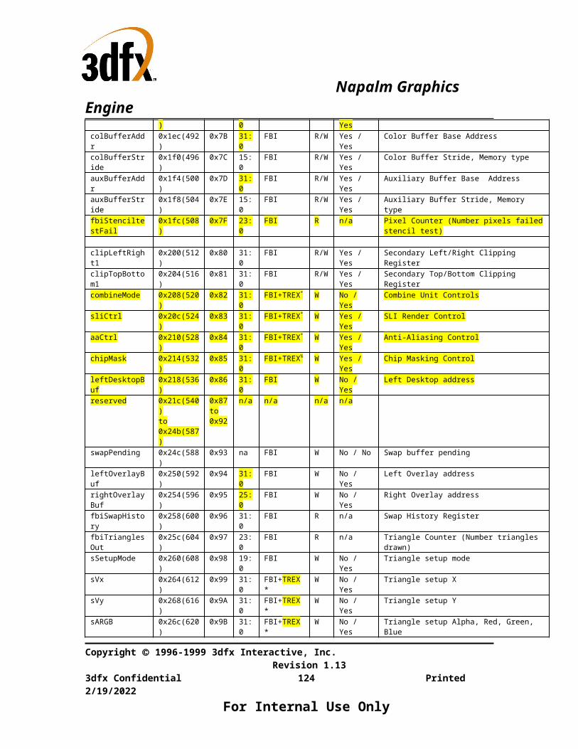
Napalm Graphics Engine
Matrix #24 12 6 148 0 10 27 15 5 1311 3 9 1
Matrix #38 4 10 60 12 2 1411 7 9 53 15 1 13
The following values are recommend for the various anti-aliasing modes supported (disable dither rotation for 32BPP rendering):
No anti-aliasing: Set renderMode[25]=0 and fogMode[19:13]=0x0
2-sample anti-aliasing (single chip or multi-chip): Set renderMode[25]=1, fogMode[13:12]=0x0, fogMode[15:14]=0x0,
fogMode[17:16]=0x2, and fogMode[19:18]=0x24-sample anti-aliasing (multi-chip only):
In the chip(s) which render(s) subsamples #0,1: Set renderMode[25]=1, fogMode[13:12]=0x0, fogMode[15:14]=0x0, fogMode[17:16]=0x1, and fogMode[19:18]=0x1
In the chip(s) which render(s) subsamples #2,3: Set renderMode[25]=1, fogMode[13:12]=0x2, fogMode[15:14]=0x2, fogMode[17:16]=0x3, and fogMode[19:18]=0x3
*** Important NOTE: Dither rotation does not work properly for 3D LFBs and FASTFILLs. Dither rotation must be disabled when performing 3D LFBs or FASTFILLs by clearing renderMode bit(25).
8.27 stencilMode RegisterThe stencilMode register controls the 3D stenciling functions of the Napalm processor. Note that the stenciling functions are only capable of being used when 32 BPP rendering is enabled (renderMode[1:0]=0x2).
Bit Description7:0 Stencil Reference Value15:8 Stencil Mask23:16 Write mask applied to any values written to the stencil buffer24 Stencil Enable (1=enable)27:25 Stencil Function (see table below)
Stencil planes enable and disable drawing on a per-pixel basis. They are typically used in multipass algorithms to achieve special effects, such as decals, outlining, and constructive solid geometry rendering. When stenciling is enabled (stencilMode bit(24)=1), the following stencil test is performed:
(STENCILref & STENCILMASK) StencilFunction (STENCILdst & STENCILMASK)where STENCILref represents the Stencil Reference Value, STENCILMASK represents the Stencil Mask, and STENCILdst represents the value in the stencil buffer. The supported stencil comparison functions (Stencil Function) are shown below:Copyright 1996-1999 3dfx Interactive, Inc. Revision 1.133dfx Confidential 124 Printed 5/7/2023
For Internal Use Only

Napalm Graphics Engine
Value Stencil Function0 Never1 Less than2 Equal3 Less than or equal4 Greater than5 Not equal6 Greater than or equal7 Always
When the stencil test fails, neither the color buffer or the depth buffer is updated, and the stencil buffer may be modified as controlled by the stencilOp register. When the stencil test passes, the color buffer and/or the depth buffer may be updated depending on the depth test, and the stencil buffer may be modified as controlled by the stencilOp register. When the stencil buffer is updated, the bits written into the stencil buffer are only those bits whose corresponding bit position in stencilMode bits(23:16) is set. See the description of the stencilOp register for more description of the stenciling operation supported by Napalm.
Note that the value in stencilMode[7:0] is used as the constant stencil value stored into the stencil buffer by the FASTFILL command.
8.28 stencilOp RegisterThe stencilOp register specifies what happens to the stored stencil value while stenciling is enabled. The stencilOp register specifies what operation to perform depending upon whether the pixel fails the stencil test, fails the depth test, or passes the depth test Note that the stenciling functions are only capable of being used when 32 BPP rendering is enabled.
Bit Description3:0 Stencil Fail operation (see table below)7:4 Stencil Z Fail operation (see table below)11:8 Stencil Z Pass operation (see table below)
The stencilOp register specifies what happens to the stencil buffer while stenciling is enabled (stencilMode bit(24)=1). If the stencil test fails, no change is made to the pixels color or depth buffers, and stencilOp bits(3:0) specify what happens to the stencil buffer contents. If the stencil test passes and the depth test fails, then stencilOp bits(7:4) specify what happens to the stencil buffer contents. Similarly, if the stencil test passes and the depth test passes, then stencilOp bits(11:8) specify what happens to the stencil buffer contents. Note that if the stencil test passes that the color and/or depth buffers are updated based on the result of the depth test. Also note that if the depth buffer is disabled that the depth check is assumed to have passed and only the Stencil Fail and Stencil Z Pass operations will be used.
Depending on whether the pixel fails the stencil test, fails the depth test, or passes the depth test, the stencil buffer value is updated as specified in the rules described above according to the operations specified in the table below:
Value Stencil Operation0 Keep1 Zero
Copyright 1996-1999 3dfx Interactive, Inc. Revision 1.133dfx Confidential 125 Printed 5/7/2023
For Internal Use Only

Napalm Graphics Engine 2 Replace3 Increment and clamp4 Decrement and clamp5 Invert6 Increment and wrap7 Decrement and wrap8-15 Reserved
8.29 sliCtrl RegisterThe sliCtrl register controls the scanline interleaving capability of Napalm.
Bit Description7:0 renderMask (unsigned value)15:8 compareMask (unsigned value)23:16 scanMask (unsigned value)25:24 # chips in SLI (log2)26 SLI enable (1=enable)31:27 reserved
When SLI is enabled (sliCtrl bit(26)=1), the register fields in sliCtrl are stored as follows:N = log2(# scanlines rendered by each chip, valid values {1,2,4,8,16,32,64,128}) [0 <= N < 8]M = log2(# chips in SLI configuration, valid values {2,4,8}) [0 < M < 4]ChipID = unique value identifying each chip in an SLI configuration (range 0-7 inclusive)renderMask (sliCtrl[7:0]) = [(# chips in SLI configuration) – 1] << NcompareMask (sliCtrl[15:8]) = chipID << NscanMask (sliCtrl[23:16]) = 2N – 1# chips in SLI, log2 (sliCtrl[25:24]) = M
Note that a combination of M and N must be selected such that renderMask, compareMask, and scanMask are 8-bit quantities (i.e. less than 256).
When SLI is enabled (sliCtrl bit(26)=1), a scanline is rendered by a particular chip when (y & renderMask) == compareMask. Also, the Y value used for address is modifed when SLI is enabled as follows to reduce the amount of frame buffer memory required for a given chip:
y’ = [(y >> M) & ~scanMask] + [y & scanMask]
8.30 aaCtrl RegisterThe aaCtrl register controls the anti-aliasing capability of Napalm.
Bit Description6:0 Triangle vertex X offset for Primary buffers (signed 3.4 format) (Default is 0x0)13:7 Triangle vertex Y offset for Primary buffers (signed 3.4 format) (Default is 0x0)20:14 Triangle vertex X offset for Secondary buffers (signed 3.4 format)27:21 Triangle vertex Y offset for Secondary buffers (signed 3.4 format)28 Render AA enable (1=enable) (Default is 0).29 Reset cmd_repeat module FIFO (1=reset) (Default is 0).30 Disable first issue of triangleCMD (1=disable)31 Automatically reset cmd_repeat module FIFO (0=enable, which is the default). Must
Copyright 1996-1999 3dfx Interactive, Inc. Revision 1.133dfx Confidential 126 Printed 5/7/2023
For Internal Use Only
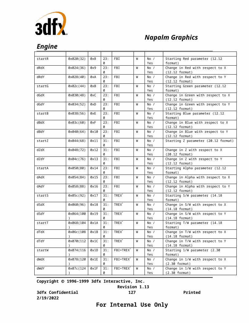
Napalm Graphics Engine
be cleared if triangle backface culling is being performed by the triangle setup unit. (Default is 0).
aaCtrl bits(13:0) specify the XY offset to the primary render buffers. Regardless of the setting of aaCtrl bit(28), all triangle XY coordinates for all vertices are added to the signed values stored in aaCtrl bits(13:0) to effectively “shift” all rendered triangles. When anti-aliased rendering is enabled (aaCtrl bit(28)=1), all rendering commands (triangle commands, Fastfill commands, and linear frame buffer writes) are all repeated a second time. The first time a rendering command is seen, it is processed unmodified (with the exception of the XY offsets specified in aaCtrl bits(13:0) being added to the triangle XY vertices, which is always enabled), using the target buffer offsets specified by the primary colBufferAddr and auxBufferAddr registers. However, when aaCtrl bit(28)=1, the rendered command will also be executed a second time, this time using the secondary colBufferAddr and auxBufferAddr registers to specify the target buffer offsets (see the colBufferAddr and auxBufferAddr registers descriptions for how the secondary buffer offsets are specified). When aaCtrl bit(28)=1 and a triangle command is received, the second triangle which is rendered into the secondary buffers will be offset using the XY offset values stored in aaCtrl bits(27:14).
When anti-aliased rendering is enabled (aaCtrl bit(28)=1), triangles will only be rendered to the secondary buffer offsets when aaCtrl bit(30) is set.
8.31 chipMask RegisterThe chipMask register controls masking writes to an entire chip
Bit Description0 Enable writes to chip #0 (1=enable). Default is 1.1 Enable writes to chip #1 (1=enable). Default is 1.2 Enable writes to chip #2 (1=enable). Default is 1.3 Enable writes to chip #3 (1=enable). Default is 1.4 Enable writes to chip #4 (1=enable). Default is 1.5 Enable writes to chip #5 (1=enable). Default is 1.6 Enable writes to chip #6 (1=enable). Default is 1.7 Enable writes to chip #7 (1=enable). Default is 1.8 Enable writes to chip #8 (1=enable). Default is 1.9 Enable writes to chip #9 (1=enable). Default is 1.10 Enable writes to chip #10 (1=enable). Default is 1.11 Enable writes to chip #11 (1=enable). Default is 1.12 Enable writes to chip #12 (1=enable). Default is 1.13 Enable writes to chip #13 (1=enable). Default is 1.14 Enable writes to chip #14 (1=enable). Default is 1.15 Enable writes to chip #15 (1=enable). Default is 1.16 Enable writes to chip #16 (1=enable). Default is 1.17 Enable writes to chip #17 (1=enable). Default is 1.18 Enable writes to chip #18 (1=enable). Default is 1.19 Enable writes to chip #19 (1=enable). Default is 1.20 Enable writes to chip #20 (1=enable). Default is 1.21 Enable writes to chip #21 (1=enable). Default is 1.22 Enable writes to chip #22 (1=enable). Default is 1.23 Enable writes to chip #23 (1=enable). Default is 1.24 Enable writes to chip #24 (1=enable). Default is 1.
Copyright 1996-1999 3dfx Interactive, Inc. Revision 1.133dfx Confidential 127 Printed 5/7/2023
For Internal Use Only

Napalm Graphics Engine 25 Enable writes to chip #25 (1=enable). Default is 1.26 Enable writes to chip #26 (1=enable). Default is 1.27 Enable writes to chip #27 (1=enable). Default is 1.28 Enable writes to chip #28 (1=enable). Default is 1.29 Enable writes to chip #29 (1=enable). Default is 1.30 Enable writes to chip #30 (1=enable). Default is 1.31 Enable writes to chip #31 (1=enable). Default is 1.
chipMask allows writes to 3D state registers, all rendering commands, and linear frame buffer accesses through the modal 3D LFB space to be masked. Up to 32 separate chips are supported, with a unique chipID specified for each chip specified by the power on strapping values {FB_DATA_14, FB_DATA_13, FB_DATA_12, FB_DATA_11, FB_DATA_10}.. To disable writes to a given chip, software writes the value 0 to the bit position in chipMask corresponding to the chip number desired to be disabled. *** Note that clearing a particular chip’s bit in chipMask only disables writes to the 3D register space and to the 3D LFB space – it does not disable writes to the 2D registers, the PCI intialization registers, the PCI configuration registers, etc.
8.32 stipple RegisterThe stipple register specifies a mask which is used to enable individual pixel writes to the RGB and depth buffers. See the stipple functionality description in the fbzMode register description for more information.
Bit Description31:0 stipple value
8.33 color0 RegisterThe color0 register specifies constant color values which are used for certain rendering functions. In particular, bits(23:0) of color0 are optionally used as the c_local input in the color combine unit. In addition, bits(31:24) of color0 are optionally used as the c_local input in the alpha combine unit. See the fbzColorPath register description for more information.
Bit Description7:0 Constant Color Blue15:8 Constant Color Green23:16 Constant Color Red31:24 Constant Color Alpha
8.34 color1 RegisterThe color1 register specifies constant color values which are used for certain rendering functions. In particular, bits(23:0) of color1 are optionally used as the c_other input in the color combine unit selected by bits(1:0) of fbzColorPath. The alpha component of color1(bits(31:24)) are optionally used as the a_other input in the alpha combine unit selected by bits(3:2) of fbzColorPath. The color1 register bits(31:0) are also used by the FASTFILL command as the constant color for screen clears. Also, for linear frame buffer write format 15(16-bit depth, 16-bit depth), the color for the pixel pipeline is taken from color1 if the pixel pipeline is enabled for linear frame buffer writes (lfbMode bit(8)=1).
Bit Description7:0 Constant Color Blue
Copyright 1996-1999 3dfx Interactive, Inc. Revision 1.133dfx Confidential 128 Printed 5/7/2023
For Internal Use Only
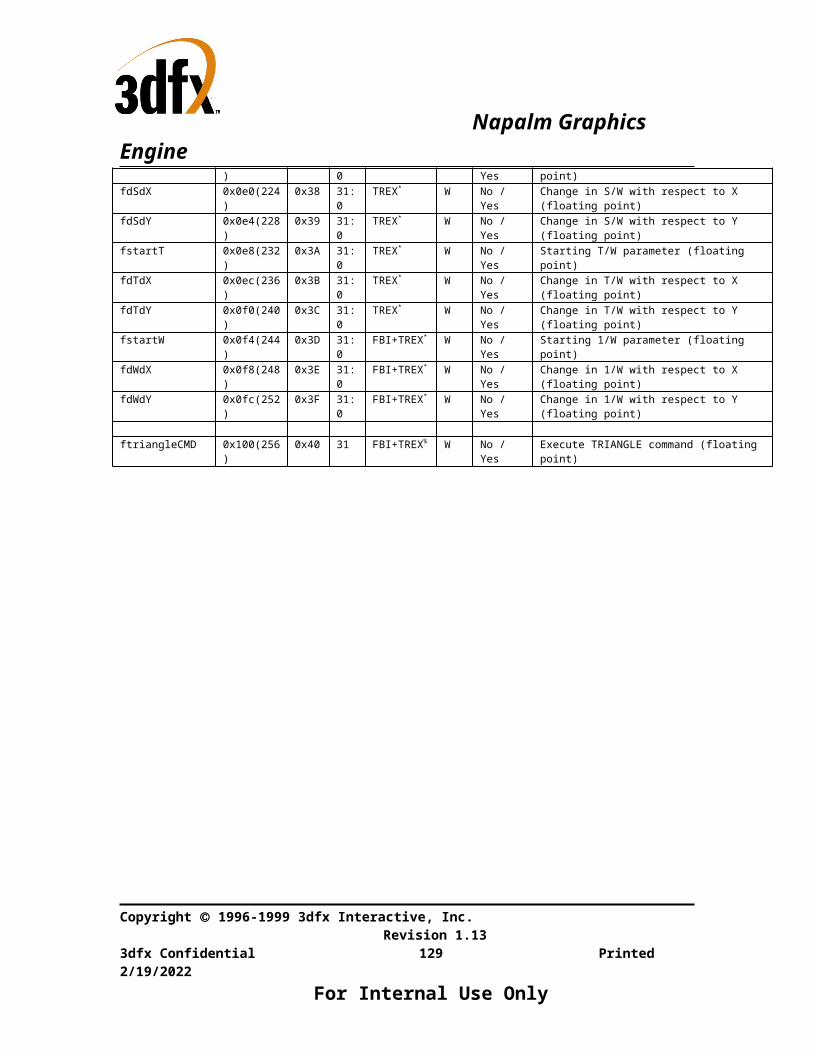
Napalm Graphics Engine 15:8 Constant Color Green23:16 Constant Color Red31:24 Constant Color Alpha
8.35 fogColor RegisterThe fogColor register is used to specify the fog color for fogging operations. Fog is enabled by setting bit(0) in fogMode. See the fogMode and fogTable register descriptions for more information fog.
Bit Description7:0 Fog Color Blue15:8 Fog Color Green23:16 Fog Color Red31:24 Reserved
8.36 zaColor RegisterThe zaColor register is used to specify constant alpha and depth values for linear frame buffer writes, FASTFILL commands, and co-planar polygon rendering support. For certain linear frame buffer access formats, the alpha and depth values associated with a pixel written are the values specified in zaColor. See the lfbMode register description for more information. When executing the FASTFILL command, the constant depth value written into the depth buffer is taken from zaColor. When 15 BPP rendering is enabled, zaColor bit(31) specifies the 1-bit alpha value that is stored into the frame buffer for the FASTFILL command (if renderMode bits(16:15)=0x2). When 32 BPP rendering is enabled, zaColor bits(23:0) are used to specify constant depth value for certain linear frame buffer writes, fastfills, and z-biasing, while when 15 or 16 BPP rendering modes are enabled, zaColor bits(15:0) are used to specify constant depth value for certain linear frame buffer writes, fastfills, and z-biasing.
Bit Description23:0 Constant Depth31:24 Constant Alpha
8.37 chromaKey RegisterThe chromaKey register specifies a color which is compared with all pixels to be written into the RGB buffer. If a color match is detected between an outgoing pixel and the chromaKey register, and chroma-keying is enabled (bit(1)=1 in the fbzMode register), then the pixel is not written into the frame buffer. An outgoing pixel will still be written into the RGB buffer if chroma-keying is disabled or the chromaKey color does not equal the outgoing pixel color. Note that the alpha color component of an outgoing pixel is ignored in the chroma-key color match circuitry. The chroma-key comparison is performed immediately after texture lookup, but before lighting, fog, or alpha blending. See the description of the fbzColorPath register for further information on the location of the chroma-key comparison circuitry.
The chromaKey register is also used to store constant color values in the texture units for texture blending. The chip fields are used to store different constant color values into each texture unit.
Bit Description7:0 Chroma-key Blue15:8 Chroma-key Green23:16 Chroma-key RedCopyright 1996-1999 3dfx Interactive, Inc. Revision 1.133dfx Confidential 129 Printed 5/7/2023
For Internal Use Only
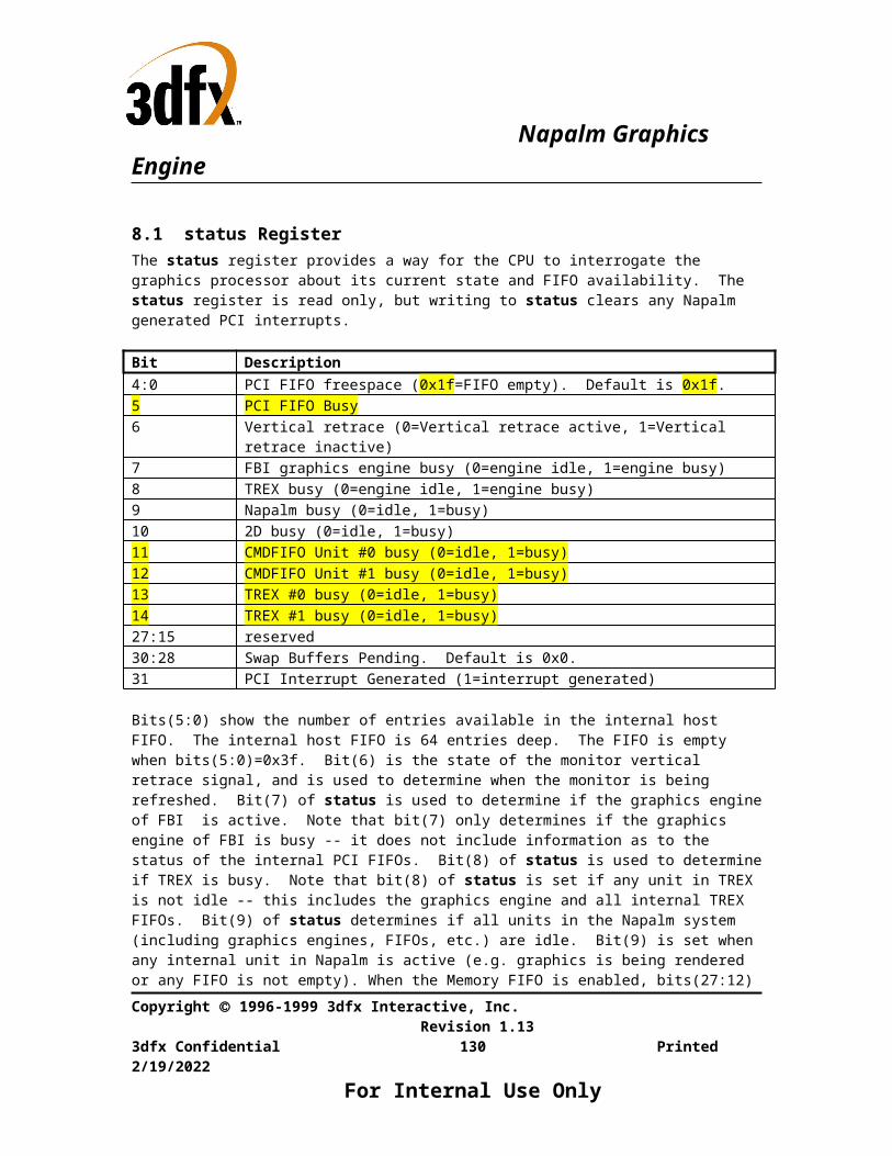
Napalm Graphics Engine 31:24 Constant Alpha (used by texture units only)
8.38 chromaRange RegisterThe chromaRange register specifies a 24-bit RGB color value which is comared to all pixels to be written to the color buffer. If chroma-keying is enabled (fbzMode[1]) and chroma-ranging is enabled (chromaRange[28]), the outgoing pixel color is compared to a color range formed by the colors of the chromaKey and chromaRange registers.
Each RGB color component of the chromaKey and chromaRange registers defines a chroma range for the color component The color component range includes the lower limit color from the chromaKey register and the upper limit color from the chromaRange register. Software must program the lower limits less-than or equal to the upper limits.
Each RGB color component chromaRange mode defines the color component range as inclusive or exclusive. Inclusive ranges prohibit colors within the range and exclusive ranges prohibit colors outside of the range.
Prohibited colors are blocked from the frame buffer based on the chromaRange mode. This mode may be set to “intersection” or “union”. The intersection mode blocks pixels prohibited by all of the color components and the union mode blocks pixels prohibited by any of the color components
The chromaRange register is also used by the texture units. When chromaRange[30:29]=0x3 and combineMode[30]=0, then texture chroma substitution is enabled. When combineMode[30]=1, then the chromaRange register is used to store constant color values in the texture units for texture blending. The chip fields are used to store different constant color values into each texture unit.
Bit Description7:0 Chroma-Range Blue Upper Limit15:8 Chroma-Range Green Upper Limit23:16 Chroma-Range Red Upper Limit
Description when combineMode[30]=024 Chroma-Range Blue Mode (0=inclusive; 1=exclusive)25 Chroma-Range Green Mode (0=inclusive; 1=exclusive)26 Chroma-Range Red Mode (0=inclusive; 1=exclusive)27 Chroma-Range Block Mode (0=intersection; 1=union)28 Chroma-Range Enable (0=disable; 1=enable)30:29 Enable texture chroma substitution (0x3=enable)31 reserved
Description when combineMode[30]=131:24 Constant Alpha (used by texture units only)
8.39 userIntrCMD RegisterWriting to the userIntrCMD register executes the USERINTERRUPT command: Bit Description0 Wait for USERINTERRUPT to be cleared before continuing (1=stall graphics engine
until interrupt is cleared)1 Wait for interrupt generated by USERINTERRUPT (visible in intrCtrl bit(11)) to be
Copyright 1996-1999 3dfx Interactive, Inc. Revision 1.133dfx Confidential 130 Printed 5/7/2023
For Internal Use Only

Napalm Graphics Engine
cleared before continuing (1=stall graphics engine until interrupt is cleared)9:2 User interrupt Tag
If the data written to userIntrCMD bit(0)=0, then a user interrupt is generated (intrCtrl bit(11) is set to 1). If the data written to userIntrCMD bit(1)=1, then the graphics engine stalls and waits for the USERINTERRUPT interrupt to be cleared before continuing processing additional commands. If no USERINTERRUPT interrupt is set and the data written to userIntrCMD bit(1)=1, then the graphics engine will not stall and will continue to process additional commands. Software may also use combinations of intrCtrl bits(1:0) to generate different functionality.
The tag associated with a user interrupt is written to userIntrCMD bits 9:2. When a user interrupt is generated, the respective tag associated with the user interrupt is read from IntrCtrl bits 19:12.
If the USERINTERRUPT command does not stall the graphics engine (userIntrCMD(0)=1), then a potential race condition occurs between multiple USERINTERRUPT commands and software user interrupt processing. In particular, multiple USERINTERRUPT commands may be generated before software is able to process the first interrupt. Irrespective of how many user interrupts have been generated, the user interrupt tag field in intrCtrl (bits 19:12) always reflects the tag of last USERINTERRUPT command processed. As a result of this behavior, early tags from multple USERINTERRUPT commands may be lost. To avoid this behavior, software may force a single USERINTERRUPT command to be executed at a time by writing userIntrCMD(1:0)=0x3 and cause the graphics engine to stall until the USERINTERRUPT interrupt is cleared.
Note that bit 5 of intrCtrl must be set to 1 for user interrupts to be generated – writes to userIntrCMD when intrCtrl(5)=0 do not generate interrupts or cause the processing of commands to wait on clearing of the USERINTERRUPT command (regardless of the data written to userIntrCMD), and are thus in effect “dropped.”
8.40 colBufferAddrThe colBufferAddr register defines the base address of the color buffer. The address must be 16-byte aligned, so colBufferAddr[3:0] are unused.
Bit Description3:0 reserved25:4 Color Buffer Base Address. Must be 16-byte aligned30:26 reserved31 Primary/secondary buffer base address select (1=secondary)
When writing to colBufferAddr, bit(31) is used to specify whether to write to the Primary or Secondary colBufferAddr register. The Secondary colBufferAddr is only used when anti-aliased rendering is enabled (aaCtrl bit(28)=1), and is used to specify the base address of a second set of buffers which is used to render primitives which are offset spatially from the Primary buffers.
8.41 colBufferStrideIf the color buffer is linear (colBufferStride[15]=0) then colBufferStride[13:0] defines the linear stride of the color buffer in bytes. Linear stride must be 16-byte aligned. If the color buffer is tiled (colBufferStride[15]=1) then colBufferStride[6:0] defines the tile stride for the color buffer in tiles.
Bit Description13:0 if [15] = 0 then
linear: [13:0] = linear stride in bytesCopyright 1996-1999 3dfx Interactive, Inc. Revision 1.133dfx Confidential 131 Printed 5/7/2023
For Internal Use Only
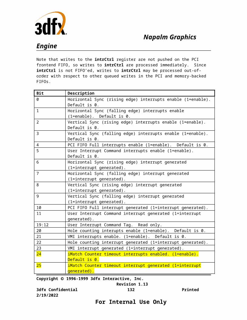
Napalm Graphics Engine
else tiled: [6:0] = tile stride in tiles; [13:7] are reserved.
14 reserved15 Memory type (0=linear; 1=tiled)
8.42 auxBufferAddrThe auxBufferAddr register defines the base address of the auxiliary buffer. The existence and enabling of the depth or the alpha auxiliary buffers is established within the fbzMode register. AuxBufferAddr must be 16 byte aligned, so auxBufferAddr[3:0] are unused.
Bit Description3:0 reserved25:4 Auxiliary Buffer Base Address. Must be 16 byte aligned30:26 reserved31 Primary/secondary buffer base address select (1=secondary)
When writing to auxBufferAddr, bit(31) is used to specify whether to write to the Primary or Secondary auxBufferAddr register. The Secondary auxBufferAddr is only used when anti-aliased rendering is enabled (aaCtrl bit(28)=1), and is used to specify the base address of a second set of buffers which is used to render primitives which are offset spatially from the Primary buffers.
8.43 auxBufferStrideIf the aux buffer is linear (auxBufferStride[15]=0) then auxBufferStride[13:0] defines the linear stride of the aux buffer in bytes. Linear stride must be 16-byte aligned. If the aux buffer is tiled (auxBufferStride[15]=1) then auxBufferStride[6:0] defines the tile stride for the aux buffer in tiles.
Bit Description13:0 if [15] = 0 then
linear: [13:0] = linear stride in byteselse tiled: [6:0] = tile stride in tiles; [13:7] are reserved.
14 reserved15 Memory type (0=linear; 1=tiled)
8.44 clipLeftRight and clipTopBottom RegistersThe clipLeftRight and clipTopBottom registers specify a rectangle within which all drawing operations are confined. If a pixel is to be drawn outside the clip rectangle, it will not be written into the RGB or depth buffers. Note that the specified clipping rectangle defines a valid drawing area in both the RGB and depth/alpha buffers. The values in the clipping registers are given in pixel units, and the valid drawing rectangle is inclusive of the clipleft and clipTop register values, but exclusive of the clipRight and clipBottom register values. clipTop must be less than clipBottom, and clipLeft must be less than clipRight. The clipLeftRight and clipTopBottom registers are be enabled by setting bit(0) in the fbzMode register. When clipping is enabled, the bounding clipping rectangle must always be less than or equal to the screen resolution in order to clip to screen coordinates. Also note that if clipping is not enabled, rendering must not be specified to occur outside of the screen resolution.
Important Note: The clipTopBottom register is defined such that y=0 always resides at the top of the monitor screen. Changing the value of the Y origin bits (fbzMode bit(17) or lfbMode bit(13)) has no affect on the clipTopBottom register orientation. As a result, if the Y origin is defined to be at the
Copyright 1996-1999 3dfx Interactive, Inc. Revision 1.133dfx Confidential 132 Printed 5/7/2023
For Internal Use Only

Napalm Graphics Engine bottom of the screen (by setting one of the Y origin bits), care must be taken in setting the clipTopBottom register to ensure proper functionality. In the case where the Y origin is defined to be at the bottom of the screen, the value of clipTopBottom is usually set as the number of scan lines in the monitor resolution minus the desired Y clipping values.
The clipLeftRight and clipTopBottom registers are also used to define a rectangular region to be drawn during a FASTFILL command. Note that when clipTopBottom is used to specify a rectangular region for the FASTFILL command, the orientation of the Y origin (top or bottom of the screen) is defined by the status of fbzMode bit(17). See section 7 and the fastfillCMD register description for more information on the FASTFILL command.
clipLeftRight RegisterBit Description11:0 Unsigned integer specifying right clipping rectangle edge (clipRight)15:12 reserved27:16 Unsigned integer specifying left clipping rectangle edge (clipLeft)31:28 reserved
clipTopBottom RegisterBit Description11:0 Unsigned integer specifying bottom clipping rectangle edge (clipBottom)15:12 reserved27:16 Unsigned integer specifying top clipping rectangle edge (clipTop)31:28 reserved
8.45 clipLeftRight1, clipTopBottom1 RegistersThe {clipLeftRight/ClipTopBottom} and {clipLeftRight1/ClipTopBottom1} registers specify two rectangular regions which restrict drawing operation. The secondary clip rectangles may be defined as inclusive or exclusive through the clipMode field of the clipTopBottom1 register. An inclusive rectangle allows drawing within the rectangle and an exclusive rectangle disallows drawing within the rectangle. Drawing within an excluded region of either of the clip rectangles circumvents the write of pixels into both the color and auxiliary buffers.
The clip registers define the four corners of a rectangular region in window relative pixel coordinates (native x/y rendering coordinates). The value of clipTop1 must be less than clipBottom1 and the value of clipLeft1 must be less than clipRight1. This programming results in a rectangular region including the clipLeft1 and clipTop1 register values, but excluding the clipRight1 and clipBottom1 register values.
The clipLeftRight1 and clipTopBottom1 registers are also used to define a rectangular clipping area when guardband clipping is enabled (renderMode bit(21)=1). Note that when guardband clipping is enabled, typically the second regular clipping rectangle defined by clipLeftRight1 and clipTopBottom1 will be disabled (clipLeftRight1 bit(31)=0). Note that when guardband clipping is enabled, the left and right edges of the clipping rectangle defined in clipLeftRight1 must be aligned on even pixel boundries.
ClipLeftRight1 Register
Bit Description11:0 Unsigned integer specifying right clipping rectangle edge (clipRight1)15:12 Reserved27:16 Unsigned integer specifying left clipping rectangle edge (clipLeft1)30:28 ReservedCopyright 1996-1999 3dfx Interactive, Inc. Revision 1.133dfx Confidential 133 Printed 5/7/2023
For Internal Use Only
Napalm Graphics Engine 31 Clip Enable (0=disable, 1=enable)
ClipTopBottom1 Register
Bit Description11:0 Unsigned integer specifying bottom clipping rectangle edge (clipBottom1)15:12 Reserved27:16 Unsigned integer specifying top clipping rectangle edge (clipTop1)30:28 Reserved31 Clip Mode (0=inclusive, 1=exclusive)
8.46 fogTable RegisterThe fogTable register is used to implement fog functions in Napalm. The fogTable register is a 64-entry lookup table consisting of 8-bit fog blending factors and 8-bit fog blending values. The fog blending values are the difference between successive fog blending factors in fogTable and are used to blend between fogTable entries. Note that the fog blending factors are stored in 6.2 format, while the fog blending factors are stored in 8.0 format. For most applications, the 6.2 format fog blending factors will have the two LSBs set to 0x0, with the six MSBs representing the difference between successive fog blending factors. Also note that as a result of the 6.2 format for the fog blending factors, the difference between successive fog blending factors cannot exceed 63. When storing the fog blending factors, the sum of each fog blending factor and fog blending factor pair must not exceed 255. When loading fogTable, two fog table entries must be written concurrently in a 32-bit word. A total of 32 32-bit PCI writes are required to load the entire fogTable register.
fogTable[n] (0 n 31)Bit Description7:0 FogTable[2n] Fog blending factor15:8 FogTable[2n] Fog blending factor23:16 FogTable[2n+1] Fog blending factor31:24 FogTable[2n+1] Fog blending factor
8.47 fbiPixelsIn RegisterThe fbiPixelsIn register is a 24-bit counter which is incremented for each pixel processed by the Napalm triangle walking engine. fbiPixelsIn is incremented irrespective if the triangle pixel is actually drawn or not as a result of the depth test, alpha test, etc. fbiPixelsIn is used primarily for statistical information, and in essence allows software to count the number of pixels in a screen-space triangle. fbiPixelsIn is reset to 0x0 on power-up reset, and is reset when a ‘1’ if written to the lsb of nopCMD.
Bit Description23:0 Pixel Counter (number of pixels processed by Napalm triangle engine)
8.48 fbiChromaFail RegisterThe fbiChromaFail register is a 24-bit counter which is incremented each time an incoming source pixel (either from the triangle engine or linear frame buffer writes through the pixel pipeline) is invalidated in the pixel pipeline because of the chroma-key color match test. If an incoming source pixel color matches the chomaKey register, fbiChromaFail is incremented. fbiChromaFail is reset to 0x0 on power-up reset, and is reset when a ‘1’ if written to the lsb of nopCMD.
Copyright 1996-1999 3dfx Interactive, Inc. Revision 1.133dfx Confidential 134 Printed 5/7/2023
For Internal Use Only
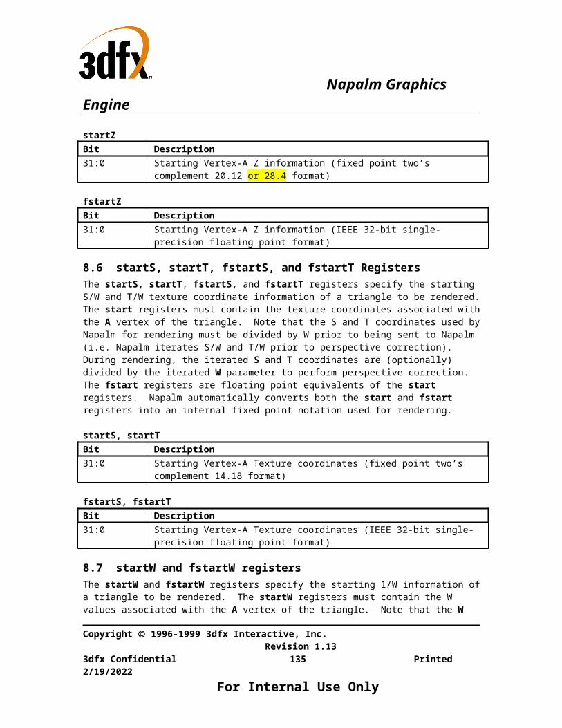
Napalm Graphics Engine Bit Description23:0 Pixel Counter (number of pixels failed chroma-key test)
8.49 fbiZfuncFail RegisterThe fbiZfuncFail register is a 24-bit counter which is incremented each time an incoming source pixel (either from the triangle engine or linear frame buffer writes through the pixel pipeline) is invalidated in the pixel pipeline because of a failure in the Z test. The Z test is defined and enabled in the fbzMode register. fbiZfuncFail is reset to 0x0 on power-up reset, and is reset when a ‘1’ if written to the lsb of nopCMD.
Bit Description23:0 Pixel Counter (number of pixels failed Z test)
8.50 fbiAfuncFail RegisterThe fbiAfuncFail register is a 24-bit counter which is incremented each time an incoming source pixel (either from the triangle engine or linear frame buffer writes through the pixel pipeline) is invalidated in the pixel pipeline because of a failure in the alpha test. The alpha test is defined and enabled in the alphaMode register. The fbiAfuncFail register is also incremented if an incoming source pixel is invalidated in the pixel pipeline as a result of the alpha masking test (bit(13) in fbzMode). fbiAfuncFail is reset to 0x0 on power-up reset, and is reset when a ‘1’ if written to the lsb of nopCMD.
Bit Description23:0 Pixel Counter (number of pixels failed Alpha test)
8.51 fbiStenciltestFail RegisterThe fbiStenciltestFail register is a 24-bit counter which is incremented each time an incoming source pixel (either from the triangle engine or linear frame buffer writes through the pixel pipeline) is invalidated in the pixel pipeline because of a failure in the stencil test. The stencil test is defined and enabled in the stencilMode register. Note that stenciling is only possible when 32 BPP rendering is enabled. fbiStenciltestFail is reset to 0x0 on power-up reset, and is reset when a ‘1’ if written to the lsb of nopCMD.
Bit Description23:0 Pixel Counter (number of pixels failed stencil test)
8.52 fbiPixelsOut RegisterThe fbiPixelsOut register is a 24-bit counter which is incremented each time a pixel is written into a color buffer during rendering operations (rendering operations include triangle commands, linear frame buffer writes, and the FASTFILL command). Pixels tracked by fbiPixelsOut are therefore subject to the chroma-test, Z test, Alpha test, etc. that are part of the regular Napalm pixel pipeline. fbiPixelsOut is used to count the number of pixels actually drawn (as opposed to the number of pixels processed counted by fbiPixelsIn). Note that the RGB mask (fbzMode bit(9) is ignored when determining fbiPixelsOut. fbiPixelsOut is reset to 0x0 on power-up reset, and is reset when a ‘1’ if written to the lsb of nopCMD.
Bit Description23:0 Pixel Counter (number of pixels drawn to color buffer)
Copyright 1996-1999 3dfx Interactive, Inc. Revision 1.133dfx Confidential 135 Printed 5/7/2023
For Internal Use Only
Napalm Graphics Engine 8.53 swapBufferPend RegisterWrites to the swapBufferPend register increments the swap buffer pending count of the Napalm status register. Writes take effect immediately and are available only through direct access.
8.54 leftOverlayBuf RegisterStarting address of left or Monocular buffer address for overlay display. For video overlay, the start address needs to be aligned on a 32-bit boundary for YUV 422 pixel format and a 64-bit boundary for YUV 411 pixel format. This register is sampled at the end of vertical retrace.
Bit Description25:0 Starting address of the overlay surface buffer 0. If overlay surface resides in linear
space, the address is the physical address.30:26 Reserved31 Bit[31] indicates if the buffer contains even or odd field in case of backend (Bob)
deinterlacing. Bit[31] = 1 for even field; Bit[31] = 0 for odd field.
8.55 RightOverlayBuf RegisterStarting address of right buffer address for overlay display. For video overlay, the start address needs to be aligned on a 32-bit boundary for YUV 422 pixel format and a 64-bit boundary for YUV 411 pixel format. This register is only used for stereo buffering. This register is sampled at the end of vertical retrace.
Bit Description25:0 Starting address of the overlay surface buffer 0. If overlay surface resides in linear
space, the address is the physical address.
8.56 leftDesktopBuf RegisterStarting address of left or Monocular buffer address for desktop display. This register is sampled at the end of vertical retrace.
Bit Description25:0 Starting address of the desktop surface buffer 0. If desktop surface resides in linear
space, the address is the physical address.30:26 Reserved31 Bit[31] indicates if the buffer contains even or odd field in case of backend (Bob)
deinterlacing. Bit[31] = 1 for even field; Bit[31] = 0 for odd field.
8.57 fbiSwapHistory RegisterThe fbiSwapHistory register keeps track of the number of vertical syncs which occur between executed swap commands. fbiSwapHistory logs this information for the last 8 executed swap commands. Upon completion of a swap command, fbiSwapHistory bits (27:0) are shifted left by four bits to form the new fbiSwapHistory bits (31:4), which maintains a history of the number of vertical syncs between execution of each swap command for the last 7 frames. Then, fbiSwapHistory bits(3:0) are updated with the number of vertical syncs which occurred between the last swap command and the just completed swap command or the value 0xf, whichever is less.
Bit Description3:0 Number of vertical syncs between the second most recently completed swap command
and the most recently completed swap command, or the value 0xf, whichever is less for Copyright 1996-1999 3dfx Interactive, Inc. Revision 1.133dfx Confidential 136 Printed 5/7/2023
For Internal Use Only

Napalm Graphics Engine
Frame N.7:4 Vertical sync swapbuffer history for Frame N-111:8 Vertical sync swapbuffer history for Frame N-215:12 Vertical sync swapbuffer history for Frame N-319:16 Vertical sync swapbuffer history for Frame N-423:20 Vertical sync swapbuffer history for Frame N-527:24 Vertical sync swapbuffer history for Frame N-631:28 Vertical sync swapbuffer history for Frame N-7
8.58 fbiTrianglesOut RegisterThe fbiTriangles register is a 24-bit counter which is incremented for each triangle processed by the Napalm triangle walking engine. Triangles which are backface culled in the triangle setup unit do not increment fbiTrianglesOut. fbiTrianglesOut is reset to 0x0 on power-up reset, and is also reset to 0x0 when a ‘1’ is written to nopCMD bit(1).
Bit Description23:0 Rendered triangles (total number of triangles rendered by Napalm triangle rendering
engine)
8.59 sSetupMode RegisterThe sSetupMode register provides a way for the CPU to only setup required parameters. When a Bit is set, that parameter will be calculated in the setup process, otherwise the value is not passed down to the triangle, and the previous value will be used. Also the definition of the triangle strip is defined in bits 21:16, where bit 16 defines fan. Culling is enabled by seting bit 17 to a value of “1”, whereas bit 18 defines the culling sign. Bit 19 disables the ping pong sign inversion that happens during triangle strips.
Bit Description0 Setup Red, Green, and Blue1 Setup Alpha2 Setup Z3 Setup Wb4 Setup W05 Setup S0 and T06 Setup W17 Setup S1 and T115:8 reserved16 Strip mode (0=strip, 1=fan)17 Enable Culling (0=disable, 1=enable)18 Culling Sign (0=positive sign, 1=negative sign)19 Disable ping pong sign correction during triangle strips (0=normal, 1=disable)
8.60 Triangle Setup Vertex RegistersThe sVx, sVy registers specify the x and y coordinates of a triangle strip to be rendered. A triangle strip, once the initial triangle has been defined, only requires a new X and Y to render consecutive triangles. The diagram below illustrates how triangle strips are sent over to Napalm.
Copyright 1996-1999 3dfx Interactive, Inc. Revision 1.133dfx Confidential 137 Printed 5/7/2023
For Internal Use Only

Napalm Graphics Engine
R
D1
D2
D3
D4
R
D1
D2
D3
D4D5
Triangle Strip Triangle Fan
1
2
34
56
7
Triangle strips and triangle fans are implemented in Napalm by common vertex information and 2 triangle commands. Vertex information is written to Napalm for a current vertex and are followed by a write to either the sBeginTriCMD or the sDrawTriCMD . For example, to render the triangle strip in the above figure, parameters X, Y, ARGB, W0, S/W, T/W for vertex R would be written followed by a write to sBeginTriCMD. Vertex D1’s parameters would next be written followed by a write to the sDrawTriCMD. After D2’s data has been sent, and the 2nd write to sDrawTriCMD has been completed Napalm will begin to render triangle 1. As triangle 1 is being rendered, data for vertex D3 will be sent down followed by another write to sDrawTriCMD, thus launching another triangle. Triangle fans are very similar to triangle strips. Instead of changing all three vertices, only the last 2 get modified. Triangle fans start with a sBeginTriCMD just as the triangle strip did, and send down sDrawTriCMD for every new vertex. To select triangle fan or triangle strip, you must write bit 0 of the triangle setup mode register.
SVx RegisterBit Description31:0 Vertex coordinate information (IEEE 32 bit single-precision floating point format)
sVy RegisterBit Description31:0 Vertex coordinate information (IEEE 32 bit single-precision floating point format)
8.61 sARGB RegisterThe ARGB register specify the color at the current vertex in a packed 32 bit value.
Bit Description31:24 Alpha Color23:16 Red Color15:8 Green Color7:0 Blue Color
8.62 sRed Registerthe sRed register is the separated red value for the current vertex.
Bit Description31:0 Red value at vertex (0.0 - 255.0). (IEEE 32 bit single-precision floating point format)
Copyright 1996-1999 3dfx Interactive, Inc. Revision 1.133dfx Confidential 138 Printed 5/7/2023
For Internal Use Only

Napalm Graphics Engine
8.63 sGreen RegisterThe sGreen register is the separated green value for the current vertex.
Bit Description31:0 Green value at vertex (0.0 - 255.0). (IEEE 32 bit single-precision floating point
format)
8.64 sBlue RegisterThe sBlue register is the separated blue value for the current vertex.
Bit Description31:0 Blue value at vertex (0.0 - 255.0). (IEEE 32 bit single-precision floating point format)
8.65 sAlpha Registerthe sAlpha register is the separated alpha value for the current vertex.
Bit Description31:0 Alpha value at vertex (0.0 - 255.0). (IEEE 32 bit single-precision floating point
format)
8.66 sVz RegisterThe Vz register is the Z value at the current vertex.
Bit Description31:0 Vertex coordinate information (IEEE 32 bit single-precision floating point format)
8.67 sWb RegisterThe Wb register is a global 1/W that is sent to both the FBI and all TMUs.
Bit Description31:0 Global 1/W. (IEEE 32 bit single-precision floating point format).
8.68 sWtmu0 RegisterThe sWtmu0 register is all the TMUs local 1/W value for the current vertex.
Bit Description31:0 Texture local 1/W. (IEEE 32 bit single-precision floating point format)
Copyright 1996-1999 3dfx Interactive, Inc. Revision 1.133dfx Confidential 139 Printed 5/7/2023
For Internal Use Only
Napalm Graphics Engine 8.69 sS/W0 RegisterThe S/W0 register is the S coordinate of the current vertex divided by W, for all TMUs.
Bit Description31:0 Texture S coordinate (IEEE 32 bit single-precision floating point format)
8.70 sT/W0 RegisterThe T/W register s the T coordinate of the current vertex divided by W, for all TMUs.
Bit Description31:0 Texture T coordinate (IEEE 32 bit single-precision floating point format)
8.71 sWtmu1 RegisterThe sWtmu1 register is TMU1’s local 1/W value for the current vertex.
Bit Description31:0 Texture local 1/W. (IEEE 32 bit single-precision floating point format)
8.72 sS/Wtmu1 RegisterThe sS/Wtmu1 register is TMU1’s local S/W value for the current vertex.
Bit Description31:0 Texture local 1/W. (IEEE 32 bit single-precision floating point format)
8.73 sT/Wtmu1 RegisterThe sT/Wtmu1 register is TMU1’s local T/W value for the current vertex.
Bit Description31:0 Texture local 1/W. (IEEE 32 bit single-precision floating point format)
8.74 sDrawTriCMD RegisterThe DrawTriCMD registers starts the draw process.
Bit Description0 Draw triangle
8.75 sBeginTriCMD RegisterA write to this register begins a new triangle strip starting with the current vertex. No actual drawing is performed.
Bit Description0 Begin New triangle
Copyright 1996-1999 3dfx Interactive, Inc. Revision 1.133dfx Confidential 140 Printed 5/7/2023
For Internal Use Only

Napalm Graphics Engine The Folowing two figures are sample pseudo code for generating triangle strips and fans. Setup Code
// packed color triangle strip setup.write (sst->sSetupMode, PACKEDCOLOR | SETUP_XY | SETUP_RGB | SETUP_ALPHA | SETUP_ST);
// Begin triangle setup// Vertex #0write (sst->sVx, -30.0);write (sst->sVy, 15.0);write (sst->sARGB, 0xFF010203); // Colorwrite (sst->sSw, 4.0);write (sst->sTw, 2.0);write (sst->sBegintriCMD, 0); // Begin Triangle
// vertex #1write (sst->sVx, 5.0);write (sst->sVy, 10.0);write (sst->sARGB, 0x00052377);write (sst->sSw, 30.0);write (sst->sTw, 60.0);write (sst->sDrawtriCMD, 0);
// Vertex #2write (sst->sVx, 50.0);write (sst->sVy, 100.0);write (sst->sARGB, 0x12345678);write (sst->sSw, 100.0);write (sst->sTw, 200.0);write (sst->sDrawtriCMD, 0);// Draw first triangle
// Vertex #3write (sst->sVx, 50.0);write (sst->sVy, 0.0);write (sst->sARGB, 0x87654321);write (sst->sSw, 0.0);write (sst->sTw, 200.0);write (sst->sDrawtriCMD, 0);// Draw second triangle
// Vertex #4write (sst->sVx, 100.0);write (sst->sVy, 100.0);write (sst->sARGB, 0x0);write (sst->sSw, 200.0);write (sst->sTw, 150.0);write (sst->sDrawtriCMD, 0);// Draw second triangle
Copyright 1996-1999 3dfx Interactive, Inc. Revision 1.133dfx Confidential 141 Printed 5/7/2023
For Internal Use Only
Napalm Graphics Engine // Separate Color triangle fan setupwrite (sst->sSetupMode, FANMODE | SETUP_XY | SETUP_RGB);
// Vertex #0write (sst->sVx, -30.0);write (sst->sVy, 15.0);write (sst->sRed, 0.0);write (sst->sGreen, 0.0);write (sst->sBlue, 0.0);write (sst->sBegintriCMD, 0); // Begin Triangle
// vertex #1write (sst->sVx, 5.0);write (sst->sVy, 10.0);write (sst->sRed, 255.0);write (sst->sGreen, 0.0);write (sst->sBlue, 0.0);write (sst->sDrawTriCMD, 0);
// Vertex #2write (sst->sVx, 50.0);write (sst->sVy, 100.0);write (sst->sRed, 0.0);write (sst->sGreen, 255.0);write (sst->sBlue, 0.0);write (sst->sDrawTriCMD, 0); // Draw first triangle
// Vertex #3write (sst->sVx, 50.0);write (sst->sVy, 0.0);write (sst->sRed, 0.0);write (sst->sGreen, 0.0);write (sst->sBlue, 255.0);write (sst->sDrawTriCMD, 0); // Draw second triangle
// Vertex #4write (sst->sVx, 100.0);write (sst->sVy, 100.0);write (sst->sRed, 255.0);write (sst->sGreen, 255.0);write (sst->sBlue, 0.0);write (sst->sDrawTriCMD, 0); // Draw second triangle
8.76 textureMode RegisterThe textureMode register controls texture mapping functionality including perspective correction, texture filtering, texture clamping, and multiple texture blending.
Bit Name Description0 tpersp_st Enable perspective correction for S and T iterators (0=linear interploation of S,T,
Copyright 1996-1999 3dfx Interactive, Inc. Revision 1.133dfx Confidential 142 Printed 5/7/2023
For Internal Use Only
Napalm Graphics Engine
force W to 1.0, 1=perspective correct, S/W, T/W)1 tminfilter Texture minification filter (0=point-sampled, 1=bilinear)2 tmagfilter Texture magnification filter (0=point-sampled, 1=bilinear)3 tclampw Clamp when W is negative (0=disabled, 1=force S=0, T=0 when W is negative)4 tloddither Enable Level-of-Detail dithering (0=no dither, 1=dither)5 tnccselect Narrow Channel Compressed (NCC) Table Select (0=table 0, 1=table 1)6 tclamps Clamp S Iterator (0=wrap, 1=clamp)7 tclampt Clamp T Iterator (0=wrap, 1=clamp)11:8 tformat Texture format (see table below)
Texture Color Combine Unit control (RGB):12 tc_zero_other Zero Other (0=c_other, 1=zero)13 tc_sub_clocal Subtract Color Local (0=zero, 1=c_local)16:14 tc_mselect Mux Select (0=zero, 1=c_local, 2=other texture alpha, 3=local texture alpha, 4=LOD,
5=LOD_frac, 6=zero, 7=c_mselect_7)17 tc_reverse_blend Reverse Blend (0=normal blend, 1=reverse blend)18 tc_add_clocal Add Color Local19 tc_add_alocal Add Alpha Local20 tc_invert_output Invert Output
Texture Alpha Combine Unit control (A):21 tca_zero_other Zero Other (0=c_other, 1=zero)22 tca_sub_clocal Subtract Color Local (0=zero, 1=c_local)25:23 tca_mselect Mux Select (0=zero, 1=c_local, 2=other texture alpha, 3=local texture alpha, 4=LOD,
5=LOD_frac, 6=iterated alpha, 7=chromaRange alpha)26 tca_reverse_blen
d Reverse Blend (0=normal blend, 1=reverse blend)
27 tca_add_clocal Add Color Local28 tca_add_alocal Add Alpha Local29 tca_invert_output Invert Output30 trilinear Enable trilinear texture mapping (0=point-sampled/bilinear, 1=trilinear)31 tcompressed Texture is compressed using either DXT1-5 or TDFX
tpersp_st bit of textureMode enables perspective correction for S and T iterators. Note that there is no performance penalty for performing perspective corrected texture mapping.
tminfilter, tmagfilter bits of textureMode specify the filtering operation to be performed. When point sampled filtering is selected, the texel specified by <s,t> is read from texture memory. When bilinear filtering is selected, the four closet texels to a given <s,t> are read from memory and blended together as a function of the fractional components of <s,t>. tminfilter is referenced when LOD>=LODmin, otherwise tmagfilter is referenced.
tclampw bit of textureMode is used when projecting textures to avoid projecting behind the source of the projection. If this bit is set, S, T are each forced to zero when W is negative. Though usually desireable, it is not necessary to set this bit when doing projected textures.
tloddither bit of textureMode enables Level-of-Detail (LOD) dither. Dithering the LOD calculation is useful when performing texture mipmapping to remove the LOD bands which can occur from with mipmapping without trilinear filtering. This adds an average of 3/8 (.375) to the LOD value and needs to compensated in the amount of lodbias.
Copyright 1996-1999 3dfx Interactive, Inc. Revision 1.133dfx Confidential 143 Printed 5/7/2023
For Internal Use Only

Napalm Graphics Engine tnccselect bit of textureMode selects the NCC lookup table to be used when decompressing 8-bit NCC textures.
tclamps, tclampt bits of textureMode enable clamping of the S and T texture iterators. When clamping is enabled, the S iterator is clamped to [0, texture width) and the T iterator is clamped to [0, texture height). When clamping is disabled, S coordinates outside of [0, texture width) are allowed to wrap into the [0, texture width) range using bit truncation. Similarly when clamping is disabled, T coordinates outside of [0, texture height) are allowed to wrap into the [0, texture height) range using bit truncation.
tformat field of textureMode specifies the texture format accessed by TREX. Note that the texture format field is used for both reading and writing of texture memory. The interpretation of the tformat field depends on the tcompressed bit. The following table shows the texture formats and how the texture data is expanded into 32-bit ARGB color when tcompressed=0:
tformat
Value
Texture format 8-bit Alpha 8-bit Red 8-bit Green 8-bit Blue
0 8-bit RGB (3-3-2) 0xff {r[2:0],r[2:0],r[2:1]} {g[2:0],g[2:0],g[2:1]} {b[1:0],b[1:0],b[1:0],b[1:0]}
1 8-bit YIQ (4-2-2) See below
2 8-bit Alpha a[7:0] a[7:0] a[7:0] a[7:0]
3 8-bit Intensity 0xff i [7:0] i[7:0] i[7:0]
4 8-bit Alpha, Intensity (4-4) {a[3:0],a[3:0]} {i[3:0],i[3:0]} {i[3:0],i[3:0]} {i[3:0],i[3:0]}
5 8-bit Palette to RGB 0xff palette r[7:0] palette g[7:0] palette b[7:0]
6 8 bit Palette to RGBA {palette_r[7:2], palette_r[7:6]
{palette_r[1:0], palette_g[7:4], palette_r[1:0]}
{palette_g[3:0], palette_b[7:6], palette_g[3:2]}
{palette_b[5:0], palette_b[5:4]}
7 Reserved
8 16-bit ARGB (8-3-3-2) a[7:0] {r[2:0],r[2:0],r[2:1]} {g[2:0],g[2:0],g[2:1]} {b[1:0],b[1:0],b[1:0],b[1:0]}
9 16-bit AYIQ (8-4-2-2) See below
10 16-bit RGB (5-6-5) 0xff {r[4:0],r[4:2]} {g[5:0],r[5:4]} {b[4:0],b[4:2]}
11 16-bit ARGB (1-5-5-5) {a[0],a[0],a[0],a[0], a[0],a[0],a[0],a[0]}
{r[4:0],r[4:2]} {g[4:0],g[4:2]} {b[4:0],b[4:2]}
12 16-bit ARGB (4-4-4-4) {a[3:0},a[3:0]} {r[3:0},r[3:0]} {g[3:0},g[3:0]} {b[3:0},b[3:0]}
13 16-bit Alpha, Intensity (8-8) a[7:0] i[7:0] i[7:0] i[7:0]
14 16-bit Alpha, Palette (8-8) a[7:0] palette r[7:0] palette g[7:0] palette b[7:0]
15 32-bit ARGB (8-8-8-8) a[7:0] r[7:0] g[7:0] b[7:0]
where a, r, g, b, and i(intensity) represent the actual values read from texture memory. The following table shows how 32-bit RGBA texture information is derived from the YIQ texture formats. This is detailed later in the nccTable description.
Texture format 8-bit Alpha 8-bit Red 8-bit Green 8-bit Blue8-bit YIQ (4-2-2) 0xff ncc _red[7:0] ncc _green[7:0] ncc _blue[7:0]16-bit AYIQ (8-4-2-2) a[7:0] ncc _red[7:0] ncc _green[7:0] ncc _blue[7:0]
When tcompressed=1, the texture format is one of the new compressed formats listed in the table below:
tformat
Value
Texture format Description
0 4-bit FXT1 Proprietary 3dfx format. Compressed alpha and color
1 4-bit DXT1 No alpha, DXT color compression with colorkeying
Copyright 1996-1999 3dfx Interactive, Inc. Revision 1.133dfx Confidential 144 Printed 5/7/2023
For Internal Use Only

Napalm Graphics Engine
2 8-bit DXT2/3 4-bit alpha, DXT color compression
3 8-bit DXT4/5 Compressed alpha, DXT color compression
4-15 Reserved unknown
For a full description of these formats, see “$/devel/sst2/docs/Subdocs/VTA Cache.doc” in SourceSafe.
There are three Texture Color Combine Units (RGB) and one Texture Alpha Combine Unit(A). The RGB Texture Color Combine Units are identical and are controlled by the same control signals. The Texture Alpha Combine Unit is slightly different architecturally, and is controlled by different control signals. The textureMode and combineMode registers are used to control the Texture Color Combine and Texture Alpha Combine Units. The diagram below illustrates the Texture Color Combine Unit:
Copyright 1996-1999 3dfx Interactive, Inc. Revision 1.133dfx Confidential 145 Printed 5/7/2023
For Internal Use Only

Napalm Graphics Engine
Copyright 1996-1999 3dfx Interactive, Inc. Revision 1.133dfx Confidential 146 Printed 5/7/2023
For Internal Use Only

Napalm Graphics Engine The diagram below illustrates the Texture Alpha Combine Unit:
Copyright 1996-1999 3dfx Interactive, Inc. Revision 1.133dfx Confidential 147 Printed 5/7/2023
For Internal Use Only
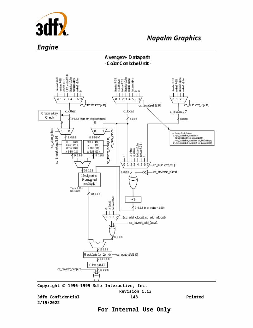
Napalm Graphics Engine
8.77 tLOD RegisterThe tLOD register controls the texture mapping LOD calculations.
Bit Name Description5:0 lodmin Minimum LOD. (4.2 unsigned)11:6 lodmax Maximum LOD. (4.2 unsigned)17:12 lodbias LOD Bias. (4.2 signed)18 lod_odd LOD odd (0=even, 1=odd)19 lod_tsplit Texture is Split. (0=texture contains all LOD levels, 1=odd or even levels only, as
controlled by lod_odd)20 lod_s_is_wider S dimension is wider, for rectilinear texture maps. This is a don’t care for square
textures. (1=S is wider than T).22:21 lod_aspect Aspect ratio. Equal to 2^n. (00 is square texture, others are rectilinear: 01 is
2x1/1x2, 10 is 4x1/1x4, 10 is 8x1/1x8)23 lod_zerofrac LOD zero frac, useful for bilinear when even and odd levels are split across two
TREXs (0=normal LOD frac, 1=force fraction to 0)24 tmultibaseaddr Use multiple texbaseAddr registers25 tdata_swizzle Byte swap incoming texture data (bytes 0<->3, 1<->2).26 tdata_swap Short swap incoming texture data (shorts 0<->1).27 reserved used to be tdirect_write in Voodoo graphics.28 tmirrors Mirror texture in S dimension29 tmirrort Mirror texture in T dimension30 tbig Large texture. Set for textures with s or t > 256
lodbias is added to the calculated LOD value, then it is clamped to the range [lodmin, min(8.0, lodmax)]. Note that whether the LOD is clamped to lodmin is used to determine whether to use the minification or magnification filter, selected by the tminfilter and tmagfilter bits of textureMode:
LOD bias, clamp
0256x256
81x1
LOD
LODmaxLODmin
tmagfiltertminfilter
Figure 1 LOD bias, tbig=0
Setting the tbig bit changes the maximum LOD. When tbig is set, LOD0 is a 2kx2k texture. In this case, lodbias is clamped to the range [lodmin, min(11.0, lodmax)].
Copyright 1996-1999 3dfx Interactive, Inc. Revision 1.133dfx Confidential 148 Printed 5/7/2023
For Internal Use Only

Napalm Graphics Engine
LOD bias, clampfor big textures
02kx2k
111x1
LOD
LODmaxLODmin
tmagfiltertminfilter
Figure 2 LOD bias, tbig=1
The tdata_swizzle and tdata_swap bits in tLOD are used to modify incoming texture data for endian dependencies. The tdata_swizzle bit causes incoming texture data bytes to be byte order reversed, such that bits(31:24) are swapped with bits(7:0), and bits(23:16) are swapped with bits(15:8). Short-word swapping is performed after byte order swizzling, and is selected by the tdata_swap bit in tLOD. When enabled, short-word swapping causes the post-swizzled 16-bit shorts to be order reversed, such that bits(31:16) are swapped with bits(15:0). The following diagram shows the data manipulation functions perfomed by the tdata_swizzle and tdata_swap bits:
Copyright 1996-1999 3dfx Interactive, Inc. Revision 1.133dfx Confidential 149 Printed 5/7/2023
For Internal Use Only
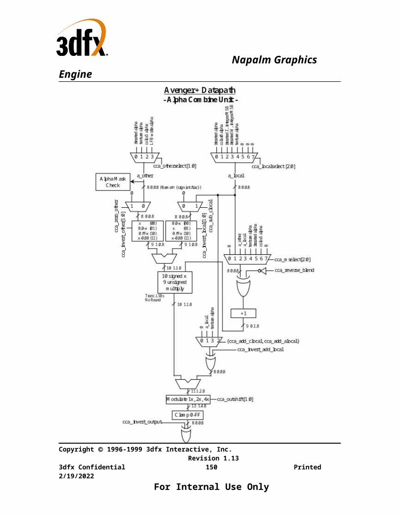
Napalm Graphics Engine
3
Incoming Texture Data
2 1 0 (Bytes 0-3)
1 01 00 10 1 tdata_swizzle
1 0 (Shorts 0-1)
0 1 1 0 tdata_swap
32
8888
8888
16
1616
16
Texture MemoryData [15:0]
Texture MemoryData [31:16]
8.78 tDetail RegisterThe tDetail register controls the detail texture.
Bit Name Description7:0 detail _max Detail texture LOD clamp (8.0 unsigned)13:8 detail_bias Detail texture bias (6.0 signed)16:14 detail_scale Detail texture scale shift left17 rgb_tminfilter RGB texture minification filter(0 = point-sampled, 1 = bilinear)18 rgb_tmagfilter RGB texture magnification filter(0 = point-sampled, 1 = bilinear)19 a_tminfilter Alpha texture minification filter(0 = point-sampled, 1 = bilinear)20 a_tmagfilter Alpha texture magnification filter(0 = point-sampled, 1 = bilinear)21 rgb_a_separate_filte
r0 = tminfilter and tmagfilter of textureMode define the filter for RGBA1 = rgb_tminfilter and rgb_tmagfilter define the filter for RGB, a_tminfilter and a_tmagfilter define the filter for alpha.
detail_factor is used in the Texture Combine Unit to blend between the main texture and the detail texture. detail_factor (0.8 unsigned) = max(detail_max, ((detail_bias - LOD) << detail_scale)).
Copyright 1996-1999 3dfx Interactive, Inc. Revision 1.133dfx Confidential 150 Printed 5/7/2023
For Internal Use Only

Napalm Graphics Engine When rgb_a_separate_filter is set, rgb_tminfilter and rgb_tmagfilter are used for RGB filtering and a_tminfilter and a_tmagfilter are used for A filtering.
8.79 texBaseAddr, texBaseAddr1, texBaseAddr2, and texBaseAddr38 RegistersThe texBaseAddr register specifies the starting texture memory address for accessing a texture. It is used for both rendering and texture downloading. Calculation of the texBaseAddr is described in the Texture Memory Access section. Selection of the base address is a function of tmultibaseaddr and LODBI.
Copyright 1996-1999 3dfx Interactive, Inc. Revision 1.133dfx Confidential 151 Printed 5/7/2023
For Internal Use Only

Napalm Graphics Engine texBaseAddr[24:4] and texBaseAddr[1] indicate the base address of the texture in 16-byte units. The 26-bit texture base address (for 64 MByte address accessibility) is formed by {texBaseAddr[1], texBaseAddr[24:4], 0000}. If the texture is tiled (texBaseAddr[0]=1), then texBaseAddr[31:25] indicate the tile stride.
texBaseAddrBit Name Description0 texmemtype Texture Memory type (0=linear, 1=tiled)1 texbaseaddr Texture Memory Base Address, bit(25, in 16-byte units, tmultibaseaddr==0 or
LODBI==03:2 Reserved24:4 texbaseaddr Texture Memory Base Address, bits(24:4), in 16-byte units, tmultibaseaddr==0 or
LODBI==031:25 texstride Tile stride (0 to 127 tiles).
texBaseAddr1, texBaseAddr2, texBaseAddr38 indicate the base addresses of lods 1, 2 and 3-8 in 16 byte units, if tmultibaseaddr=1.
texBaseAddr1, texBaseAddr2, texBaseAddr38Bit Name Description25:4 Texbaseaddr1 Texture Memory Base Address, tmultibaseaddr==1 and LODBI==125:4 texbaseaddr2 Texture Memory Base Address, tmultibaseaddr==1 and LODBI==225:4 texbaseaddr38 Texture Memory Base Address, tmultibaseaddr==1 and LODBI>=3.
8.80 trexInit1 RegisterThe trexInit1 register is used for hardware initialization and configuration of the TREX portion of Napalm.
Bit Name Description0 rsv_sl_int_slave reserved1 rsv_sl_int_en reserved6:2 ft_FIFO_sil FBI-to-TREX interface FIFO stall input level. Free space level at which stall
signal is sent back to transmitting chip. 10:7 tt_FIFO_sil TREX-to-TREX interface FIFO stall input level. Free space level at which
stall signal is sent back to transmitting chip. 11 reserved15:12 tf_ck_del_adj TREX-to-FBI interface clock delay adjust. Adjusts phase of the transmit
clock.16 rg_ttcii_inh Register ttcii inhibit. when use_rg_ttcii_inh==1. 0=expect data from upstream
TREX, 1=ignore data from upstream TREX.17 use_rg_ttcii_inh Use register ttcii inhibit to chose if data is expected from upstream TREX.
0=use clock sense result, 1=ignore clock sense result and use rg_ttcii_inh.18 send_config Send config. Transmit configuration to FBI through the tf_ interface instead
of texel data. 0=normal, 1=send.19 reset_FIFOs Reset all of the FIFO’s inside TREX. 0=run, 1=assert the reset signal.20 reset_graphics Reset all of the graphics inside TREX. 0=run, 1=assert the reset signal.22:21 rsv_palette_del reserved25:23 send_config_sel Send config select. (not revision 0) Selects which data to transmit to FBI
when send_config==1. Copyright 1996-1999 3dfx Interactive, Inc. Revision 1.133dfx Confidential 152 Printed 5/7/2023
For Internal Use Only
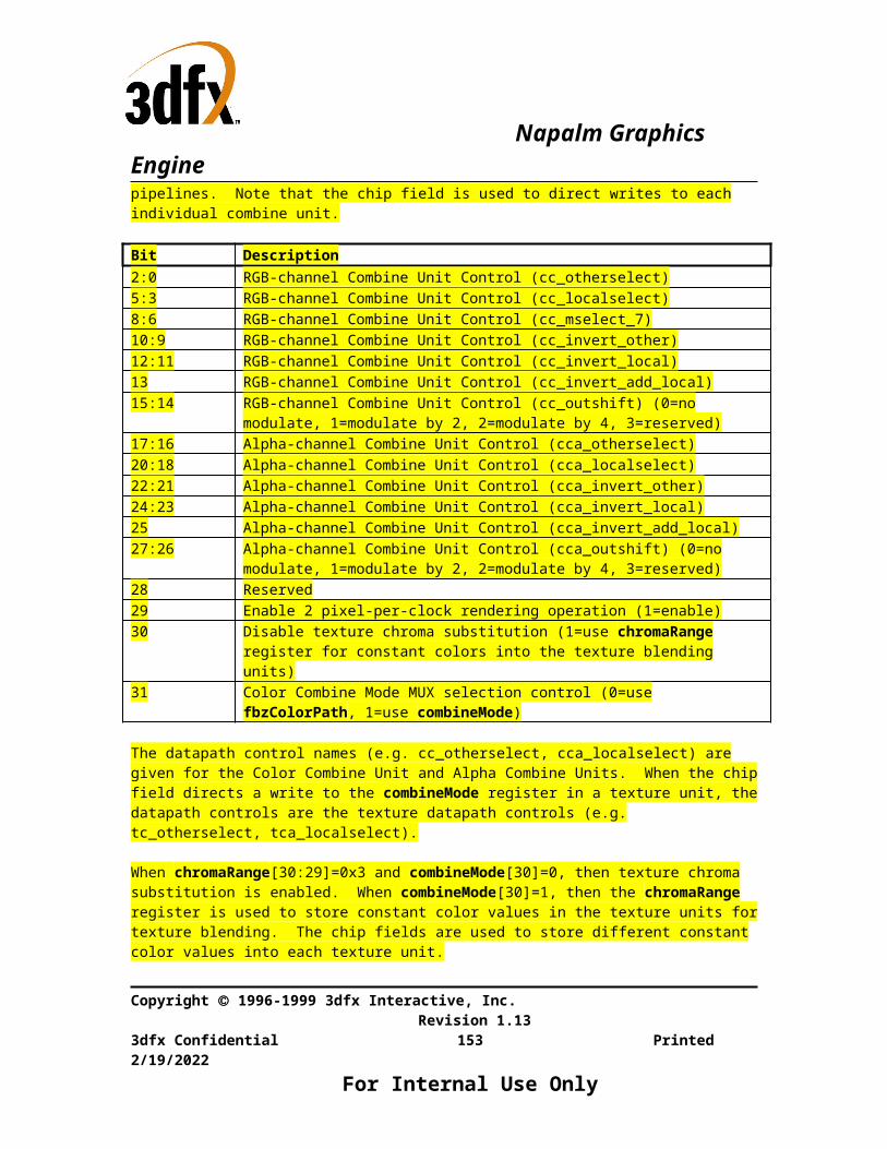
Napalm Graphics Engine
000=reserved001=reserved010=reserved011=trexInit1, 100=texBaseAddr[31:0], (for this function, 32 bits are retained and is non-maskable)101,110,111=reserved.
26 use_4bit_st_frac 1=use 4 bits for s,t instead of 8. Default = 0.27 a_attr_set_only 1=use only the A set of triangle attributes. Default = 0.28 nop_per_tri 1=insert a nop per triangle. Default = 0.29 always_cache_inv 1=always cache invalidate each triangle. Default = 0.30 always_4texel_needed 1=always indicate that 4 texels are needed for each pixel. Default = 0.
send_configIt is possible to read trexInit1 and texBaseAddr through the the send_config path, which sends these registers over to the FBI section of Napalm via the graphics tf bus. When send_config = 1, tf_data[31:0] = {a[7:0], r[7:0], g[7:0], b[7:0]}. TREX’s TC/TCA must be set to pass c_other.
8.81 nccTable0 and nccTable1 RegistersThe nccTable0 and nccTable1 registers contain two Narrow Channel Compression (NCC) tables used to store lookup values for compressed textures (used in YIQ and AYIQ texture formats as specified in tformat of textureMode). Two tables are stored so that they can be swapped on a per-triangle basis when performing multi-pass rendering, thus avoiding a new download of the table. Use of either nccTable0 or nccTable1 is selected by the Narrow Channel Compressed (NCC) Table Select bit of textureMode. nccTable0 and nccTable1 are stored in the format of the table below, and are write only.
nccTable Address Bits Contents0 31:0 {Y3[7:0], Y2[7:0], Y1[7:0], Y0[7:0]}1 31:0 {Y7[7:0], Y6[7:0], Y5[7:0], Y4[7:0]}2 31:0 {Yb[7:0], Ya[7:0], Y9[7:0], Y8[7:0]}3 31:0 {Yf[7:0], Ye[7:0], Yd[7:0], Yc[7:0]}4 26:0 {I0_r[8:0], I0_g[8:0], I0_b[8:0]}5 26:0 {I1_r[8:0], I1_g[8:0], I1_b[8:0]}6 26:0 {I2_r[8:0], I2_g[8:0], I2_b[8:0]}7 26:0 {I3_r[8:0], I3_g[8:0], I3_b[8:0]}8 26:0 {Q0_r[8:0], Q0_g[8:0], Q0_b[8:0]}9 26:0 {Q1_r[8:0], Q1_g[8:0], Q1_b[8:0]}
10 26:0 {Q2_r[8:0], Q2_g[8:0], Q2_b[8:0]}11 26:0 {Q3_r[8:0], Q3_g[8:0], Q3_b[8:0]}
The following figure illustrates how compressed textures are decompressed using the NCC tables:
Copyright 1996-1999 3dfx Interactive, Inc. Revision 1.133dfx Confidential 153 Printed 5/7/2023
For Internal Use Only

Napalm Graphics Engine
(2x16)x8 LookupRAM
4 Y
8
(2x4)x27 LookupRAM
2 I
27
(2x4)x27 LookupRAM
2 Q
27
8
8 9 Red 9 Red 8 9 Grn 9 Grn 8 9 Blu 9 Blu
8 Red 8 Green 8 Blue
11
Clamp 0-FF
8
11
Clamp 0-FF
8
11
Clamp 0-FF
8
0.8 1.8 1.8
0.8
nccTable registerSelect
From Memory Data Alignment
8.82 8-bit PaletteThe 8-bit palette is used for 8-bit P and 16-bit AP modes. The palette is loaded with register writes. During rendering, four texels are looked up simultaneously, each an independent 8-bit address.
Palette Write
The palette is written through the NCC table 0 I and Q register space when the MSB of the register write data is set. The NCC tables are not written when the I or Q NCC table register space is addressed and MSB of the register write data is set to 1 – Instead the data is stored in the texture palette.
Copyright 1996-1999 3dfx Interactive, Inc. Revision 1.133dfx Confidential 154 Printed 5/7/2023
For Internal Use Only

Napalm Graphics Engine
Palette Load Mechanism
nccTable0 I0
31 0
G[7:0] B[7:0]1 R[7:0]P[7:1]P[0]=0
Register Write DataRegisterAddress LSB of P
nccTable0 I1 G[7:0] B[7:0]1 R[7:0]P[7:1]P[0]=1
nccTable0 I2 G[7:0] B[7:0]1 R[7:0]P[7:1]P[0]=0
nccTable0 I3 G[7:0] B[7:0]1 R[7:0]P[7:1]P[0]=1
nccTable0 Q0 G[7:0] B[7:0]1 R[7:0]P[7:1]P[0]=0
nccTable0 Q1 G[7:0] B[7:0]1 R[7:0]P[7:1]P[0]=1
nccTable0 Q2 G[7:0] B[7:0]1 R[7:0]P[7:1]P[0]=0
nccTable0 Q3 G[7:0] B[7:0]1 R[7:0]P[7:1]P[0]=1
Note that the even addresses alias to the same location, as well as the odd ones. It is recommended that the table be written as 32 sets of 8 so that PCI bursts can be 8 transfers long.
8.83 Command Descriptions
8.83.1 NOP CommandThe NOP command is used to flush the graphics pipeline. When a NOP command is executed, all pending commands and writes to the texture and frame buffers are flushed and completed, and the graphics engine returns to its IDLE state. While this command is used primarily for debugging and verification purposes, it is also used to clear the 3D status registers (fbiTriangles, fbiPixelsIn, fbiPixelsOut, fbiChromaFail, fbiZfuncFail, and fbiAfuncFail). Setting nopCMD bit(0)=1 clears the 3D status registers and flushes the graphics pipeline, while setting nopCMD bit(0)=0 has no affect on the 3D status registers but flushes the graphics pipeline. See the description of the nopCMD register in section 5 for more information.
8.83.2 TRIANGLE CommandTO BE COMPLETED.
Copyright 1996-1999 3dfx Interactive, Inc. Revision 1.133dfx Confidential 155 Printed 5/7/2023
For Internal Use Only
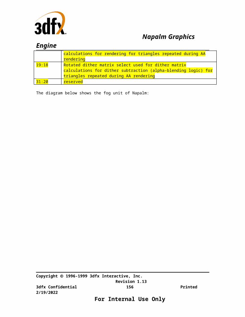
Napalm Graphics Engine 8.83.3 FASTFILL CommandThe FASTFILL command is used for screen clears. When the FASTFILL command is executed, the depth-buffer comparison, alpha test, alpha blending, and all other special effects are bypassed and disabled. Prior to executing the FASTFILL command, the clipLeftRight and clipTopBottom registers must be loaded with a rectanglar area which is desired to be cleared -- -- the fastfillCMD register is then written to initiate the FASTFILL command. Note that clip registers define a rectangular area which is inclusive of the clipLeft and clipTop register values, but exclusive of the clipRight and clipBottom register values. Note also that the relative position of the Y origin (either top of bottom of the screen) is defined by fbzMode bit(17), and that fbzMode bits(15:14) determine which RGB buffer (front or back) is written.
When running in 15 or 16 BPP rendering modes, the FASTFILL command uses the status of the RGB write mask (bit(9) of fbzMode) and the depth-buffer write mask (bit(10) of fbzMode) to access the RGB/depth-buffer memory. The 24-bit color specified in Color1(23:0) is written to the RGB buffer (with optional dithering as specified by bit(8) of fbzMode, but optionally overriden by bit(0) of the fastfillCMD register), and the depth value specified in zaColor(15:0) is written to the depth buffer.
When running in 15 BPP rendering mode, the 1-bit alpha value stored into the frame buffer is calculated as follows:
- zaColor bit(31) if renderMode[16:15]=0x2- 1 if renderMode[16:15]=0x1- 0 if renderMode[16:15]=0x0
When running in 32 BPP rendering mode, the FASTFILL command uses the status of the RGBA write mask (fbzMode bit(9)) and the individual alpha/color write masks in renderMode bits(20:17) to enable writes to the each individual alpha and color planes. Note that fbzMode bit(9) must be set to allow writes to any of the alpha or color planes when running in 32 BPP rendering mode. The value in color1(31:0) is stored into the alpha and color planes, as controlled by each individual write mask. Writes to the 24-bit depth value are enabled by setting fbzMode bit(10), with the value of zaColor(23:0) stored into the 24-bit depth buffer. Finally, writes to the stencil buffer are controlled by the stencil write mask field in the stencilMode register (bits(23:16)) – setting any bit in stencilMode bits(23:16) allows the stencil buffer to be updated. Note that individual bit write masking of the stencil buffers is not supported for the FASTFILL command. The stencil reference value (stencilMode bits(7:0)) is stored into the 8-bit stencil buffer, as controlled by the stencil write mask field.
See the description of the fastfillCMD register for more information.
8.83.4 SWAPBUFFER Command The SWAPBUFFER command is used to swap the drawing buffers to enable smooth animation. Since the SWAPBUFFER command is executed and queued like all other 2D and 3D commands, proper order is maintained and software does not have to poll and wait for vertical retrace to manually swap buffers – this frees the CPU to perform other functions while the graphics engine automatically waits for vertical retrace. When the SWAPBUFFER command is executed, swapbufferCMD bit(0) determines whether the drawing buffer swapping is synchronized with vertical retrace. Typically, it is desired that buffer swapping be synchronized with vertical retrace to eliminate frame “tearing” typically found on single buffered displays. If vertical retrace synchronization is enabled for double buffered applications, the graphics command processor blocks on a SWAPBUFFER command until the monitor vertical retrace signal is active. If the number of vertical retraces seen exceeds the value stored in bits(8:1) of swapbufferCMD, then the pointer used by the monitor refresh control logic is changed to point to another drawing buffer. If vertical retrace synchronization is enabled for triple buffered applications, the graphics processor does not block on a SWAPBUFFER command. Instead, a flag is set in the monitor
Copyright 1996-1999 3dfx Interactive, Inc. Revision 1.133dfx Confidential 156 Printed 5/7/2023
For Internal Use Only
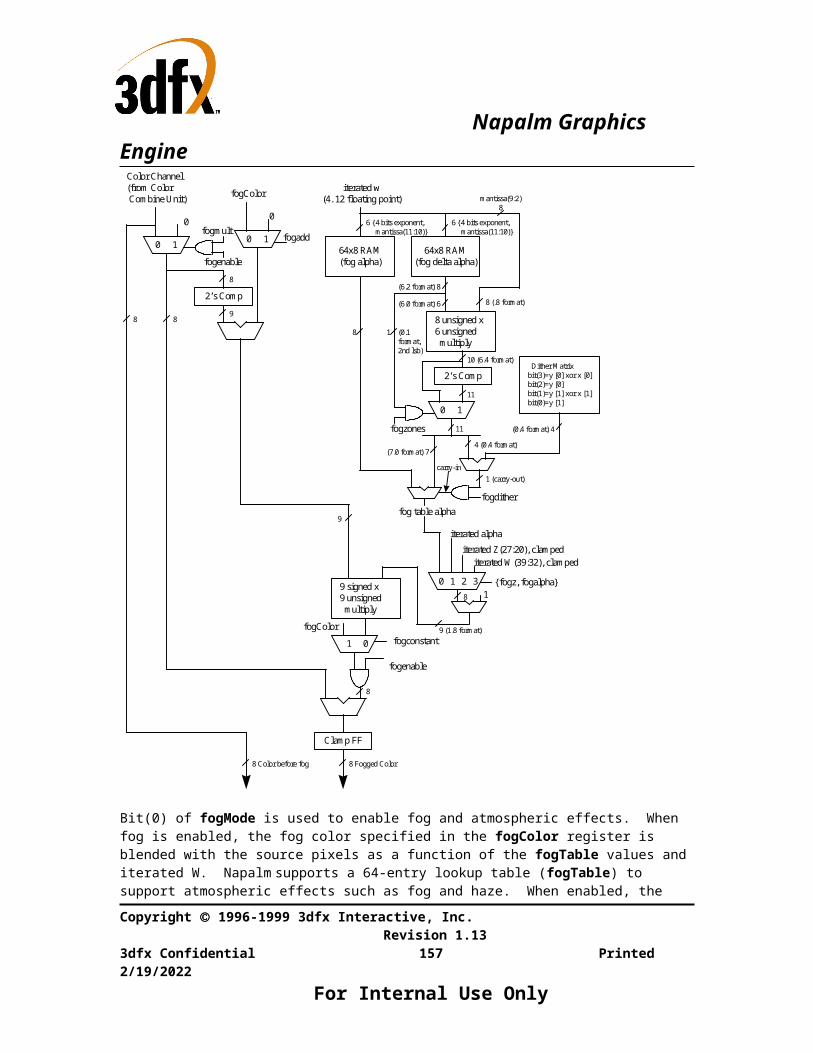
Napalm Graphics Engine refresh control logic that automatically causes the data pointer to be modified in the monitor refresh control logic during the next active vertical retrace period. Using triple buffering allows rendering operations to occur without waiting for the vertical retrace active period.
The swapbufferCMD must be proceeded by a direct write of the swapPend register. A write to the swapPend register increments the swap buffers pending field in the status registers. Conversely, when an actual frame buffer swapping occurs, the swap buffers pending field in the status register is decremented. The swap buffers pending field allows software to determine how many SWAPBUFFER commands are present in the Napalm FIFOs. See the descript of the swapbufferCMD register in section 5 for more information.
Since Napalm does not have fixed color buffer locations, 2 new registers are required for buffer display. LeftOverlayBuf and rightOverlayBuf are used by the video scanout section to determine the location of the current display buffer. The sequence of writes for double buffering would consist of writing to the leftOverlayBuf register and optionally the rightOverlayBuf (for stereo operations), followed by a direct write of swapPend, ending with a write to swapbufferCMD register. The leftOverlayBuf and rightOverlayBuf registers are fifoed, allowing tripple and quad buffering.
8.83.5 USERINTERRUPT CommandThe USERINTERRUPT command allows for software-generated interrupts. A USERINTERRUPT command is generated by writing to the userIntrCMD register. userIntrCMD bit(0) controls whether a write to userIntrCMD generates a USERINTERRUPT. Setting userIntrCMD bit(0)=1 generates a USERINTERRUPT. userIntrCMD bit(1) determines whether the graphics engine stalls on software clearing of the user interrupt. By setting userIntrCMD bit(1)=1, the graphics engine stalls until the USERINTERRUPT is cleared. Alternatively, setting userIntrCMD bit(1)=0 does not stall the graphics engine upon execution of the USERINTERRUPT command, and additional graphics commands are processed without waiting for clearing of the user interrupt. A identification, or Tag, is also associated with an individual USERINTERRUPT command, and is specified by writing an 8-bit value to userIntrCMD bits(9:2).
User interrupts must be enabled before writes to the userIntrCMD are allowed by setting intrCtrl bit(5)=1. Writes to userIntrCMD when intrCtrl bit(5)=0 are “dropped” and do not affect functionality. A user interrupt is detected by reading intrCtrl bit (11), and is cleared by setting intrCtrl bit(11)=0. The tag of a generated user interrupt is read from intrCtrl bits (19:12). See the description of the intrCtrl and userIntrCMD registers in section 5 for more information.
8.84 Linear Frame Buffer Access (* FIX THIS *)The Napalm linear frame buffer base address is located at a 8 Mbyte offset from the memBaseAddr PCI configuration register and occupies 4 Mbytes of Napalm address space (see section 4 for an Napalm address map). Regardless of actual frame buffer resolution, all linear frame buffer accesses assume a 2048-pixel logical scan line width. The number of bytes per scan line depends on the format of linear frame buffer access format selected in the lfbMode register. Note for all accesses to the linear frame buffer, the status of bit(16) of fbzMode is used to determine the Y origin of data accesses. When bit(16)=0, offset 0x0 into the linear frame buffer address space is assumed to point to the upper-left corner of the screen. When bit(16)=1, offset 0x0 into the linear frame buffer address space is assumed to point to the bottom-left corner of the screen. Regardless of the status of fbzMode bit(16), linear frame buffer addresses increment as accesses are performed going from left-to-right across the screen. Also note that clipping is not automatically performed on linear frame buffer writes if scissor clipping is not explicitly enabled (fbzMode bit(0)=1). Linear frame buffer writes to areas outside of the monitor resolution when clipping is disabled result in undefined behavior.
Copyright 1996-1999 3dfx Interactive, Inc. Revision 1.133dfx Confidential 157 Printed 5/7/2023
For Internal Use Only
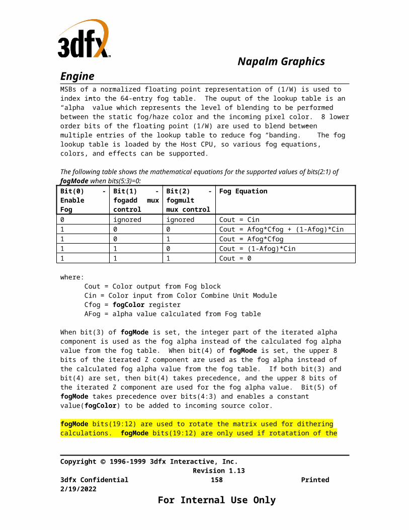
Napalm Graphics Engine 8.84.1 Linear frame buffer WritesThe following table shows the supported linear frame buffer write formats as specified in bits(3:0) of lfbMode:
Value Linear Frame Buffer Access Format16-bit formats
0 16-bit RGB (5-6-5)1 16-bit RGB (x-5-5-5)2 16-bit ARGB (1-5-5-5)3 Reserved
32-bit formats4 24-bit RGB (8-8-8)5 32-bit ARGB (8-8-8-8)7:6 Reserved11:8 Reserved12 16-bit depth, 16-bit RGB (5-6-5)13 16-bit depth, 16-bit RGB (x-5-5-5)14 16-bit depth, 16-bit ARGB (1-5-5-5)15 16-bit depth, 16-bit depth When writing to the linear frame buffer with a 16-bit access format (formats 0-3 and format 15 in lfbMode), each pixel written is 16-bits, so there are 2048 bytes per logical scan line. Remember when utilizing 16-bit access formats, two 16-bit values can be packed in a single 32-bit linear frame buffer write -- the location of each 16-bit component in screen space is defined by bit(11) of lfbMode. When using 16-bit linear frame buffer write formats 0-3, the depth components associated with each pixel is taken from the zaColor register. When using 16-bit format 3, the alpha component associated with each pixel is taken from the 16-bit data transfered, but when using 16-bit formats 0-2 the alpha component associated with each pixel is taken from the zaColor register. The format of the individual color channels within a 16-bit pixel is defined by the RGB channel format field in lfbMode bits(12:9). See the lfbMode description in section 5 for a detailed description of the rgb channel format field.
When writing to the linear frame buffer with 32-bit access formats 4 or 5, each pixel is 32-bits, so there are 4096 bytes per logical scan line. Note that when utilizing 32-bit access formats, only a single pixel may be written per 32-bit linear frame buffer write. Also note that linear frame buffer writes using format 4 (24-bit RGB (8-8-8)), while 24-bit pixels, must be aligned to a 32-bit (doubleword) boundary -- packed 24-bit linear frame buffer writes are not supported by Napalm. When using 32-bit linear frame buffer write formats 4-5, the depth components associated with each pixel is taken from the zaColor register. When using format 4, the alpha component associated with each pixel is taken from the zaColor register, but when using format 5 the alpha component associated with each pixel is taken from the 32-bit data transfered. The format of the individual color channels within a 24/32-bit pixel is defined by the rgb channel format field in lfbMode bits(12:9).
When writing to the linear frame buffer with a 32-bit access formats 12-14, each pixel is 32-bits, so there are 4096 bytes per logical scan line. Note that when utilizing 32-bit access formats, only a single pixel may be written per 32-bit linear frame buffer write. If depth or alpha information is not transfered with the pixel, then the depth/alpha information is taken from the zaColor register. The format of the individual color channels within a 24/32-bit pixel is defined by the rgb channel format field in lfbMode bits(12:9). The location of each 16-bit component of formats 12-15 in screen space is defined by bit(11)
Copyright 1996-1999 3dfx Interactive, Inc. Revision 1.133dfx Confidential 158 Printed 5/7/2023
For Internal Use Only
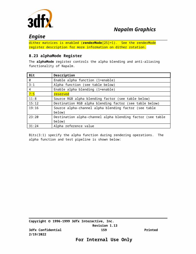
Napalm Graphics Engine of lfbMode. See the lfbMode description in section 5 for more information about linear frame buffer writes.
8.84.2 Linear frame buffer Reads It is important to note that reads from the linear frame buffer bypass the PCI host FIFO (as well as the memory FIFO if enabled) but are blocking. If the host FIFO has numerous commands queued, then the read can potentially take a very long time before data is returned, as data is not read from the frame buffer until the PCI host FIFO is empty and the graphics pixel pipeline has been flushed. One way to minimize linear frame buffer read latency is to guarantee that the Napalm graphics engine is idle and the host FIFOs are empty (in the status register) before attempting to read from the linear frame buffer.
9. 1. PLL Registers
Register Name Address Bits R/W DescriptionpllCtrl0 0x40-0x43 31:0 R/W Video Clock PLLpllCtrl1 0x44-0x47 31:0 R/W GRX Clock PLL
Genlock mode: in order for the register 3da (vga register) to reflect the status of vsync correct, vgaInit0[1]
needs to be set
1.1 PllCtrl0, PllCtrl1 registersThese registers control the frequency of the core clock (GRX Clock) and the Video Clock.
Bit Description1:0 K, Post divider value7:2 M, PLL input divider15:8 N, PLL multiplier16 Test. (0=normal operation, 1 = CLK is output of VCO). Default = 0.
Frequency output of PLL’s is given:
Copyright 1996-1999 3dfx Interactive, Inc. Revision 1.133dfx Confidential 159 Printed 5/7/2023
For Internal Use Only
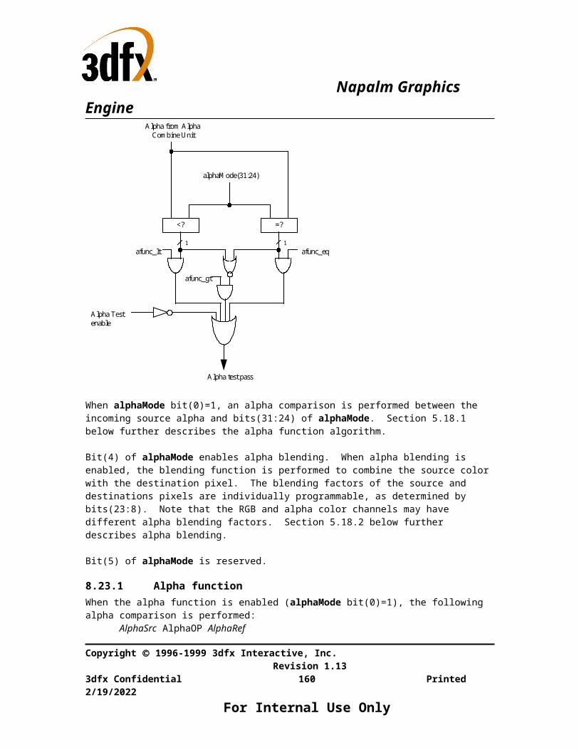
Napalm Graphics Engine
fout = 14.31818 * (N + 2) / (M + 2) / (2 ^ K).
NOTE: if the deviceID==4, then the GRX clock pll’s M[7:2] value is forced to 0x18 (24 decimal), which limits the maximum frequency of the grx_clk to 141MHz. Software must adjust calculations for setting the frequency accordingly.
1.2 TK532_PLL Modifications for NapalmIn the 532 PLL, there are a few design changes that need to be made to allow complete testing of the PLL. To be specific, both Habenero and Napalm use the 532 Mhz output of the PLL, which is not accesablie in the previous design. The 133Mhz clock, on the other hand is unused. In this design, the same three bits are used for the mux selects, but are allocated differently.
Simplified Block Diagram of the PLL (no Phase Compare, Charge pump or REF / FBCLK prescale shown):
These are the modes that will be used in the PLL:
PLL_EN S0 S1 S2 CLK66 CLK266 CLK532 Mode0 0 0 0 0 0 0 PLL Disablex 1 1 1 TestCLK2 TestCLK1 TestCLK0 PLL Bypass mode1 0 0 0 Ref Ref*4 Ref*8 Close loop1 1 0 0 TestCLK0/8 TestCLK0/2 TestCLK0
9.1 Test Mode
All outputs need to be phase aligned. In reality, all TestCLK inputs are tied together at the boundry of the PLL. PLL_EN is required to guarantee a known phase relationship for CLK66 and CLK266 when in Test Mode.
Copyright 1996-1999 3dfx Interactive, Inc. Revision 1.133dfx Confidential 160 Printed 5/7/2023
For Internal Use Only
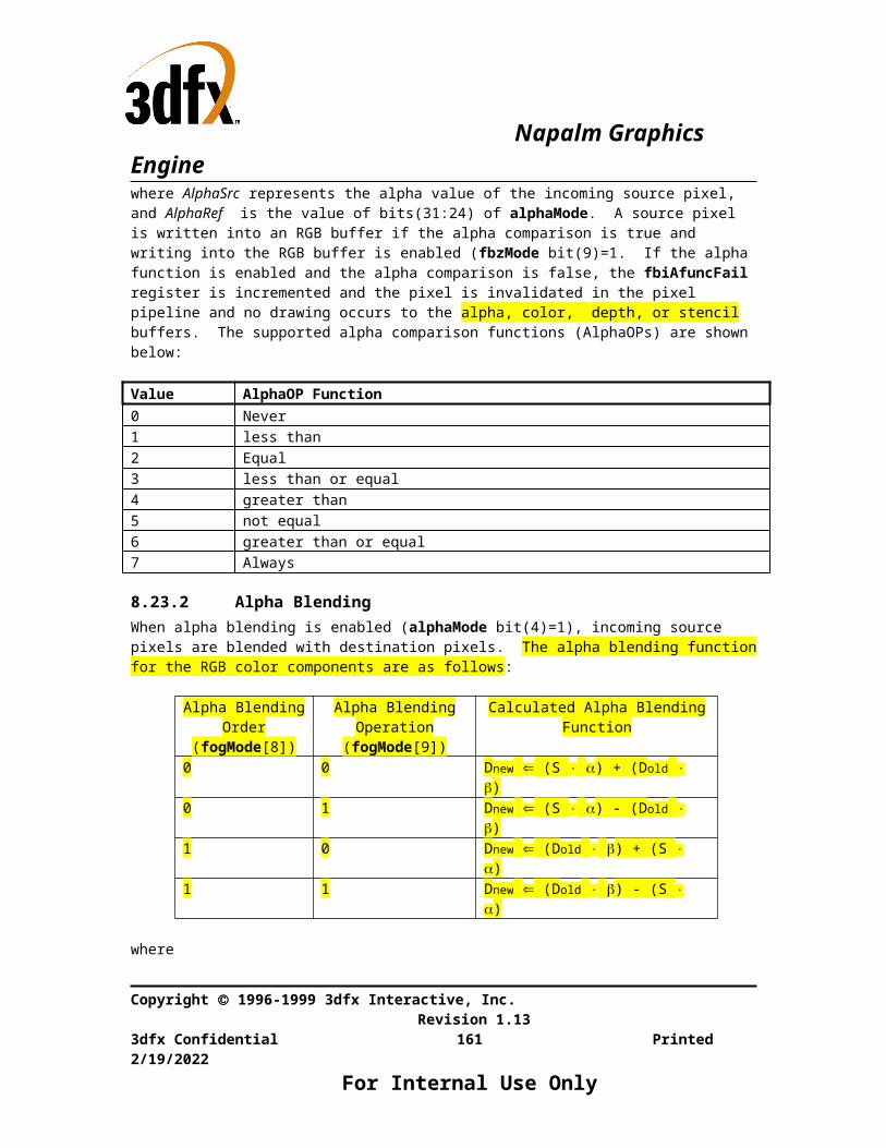
Napalm Graphics Engine
Copyright 1996-1999 3dfx Interactive, Inc. Revision 1.133dfx Confidential 161 Printed 5/7/2023
For Internal Use Only
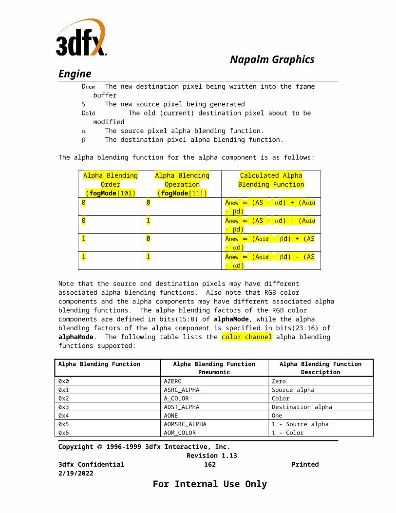
Napalm Graphics Engine
10. 2. DAC Registers Register Name I/O
AddressBits R/W Description
dacMode 0x4c-0x4f 4:0 R/W Dac Mode 2:1 or 1:1dacAddr 0x50-0x53 8:0 R/W Dac pallette addressdacData 0x54-0x57 23:0 R/W Dac data registerreserved 0x58-0x5b na
10.1 2.1 dacModeBit Description0 Dac Mode 2:1 or 1:11 Enable DPMS on Vsync2 Force Vsync value.3 Enable DPMS on Hsync4 Force Hsync value.
10.2 2.2 dacAddrBit Description8:0 Pallette Address
This is the 9 bit CLUT address used for programming the CLUT. Unlike the VGA mechanism, this address does not auto increment, but has access to the entire 512 entries in the CLUT.
10.3 2.3 dacDataBit Description23:0 Dac color value
This is the 24 bit RGB value at the index programmed into dacAddr. The color values are always stored with red in bits [23:16], green in bits [15:8] and blue in bits [7:0].
Copyright 1996-1999 3dfx Interactive, Inc. Revision 1.133dfx Confidential 162 Printed 5/7/2023
For Internal Use Only
Napalm Graphics Engine
11. 3. Video Registers(PCI) Register Name I/O
AddrBits R/W Description
vidTvOutBlankVCount 0x3c 31:0 R/W TV Out Vertical Active Start/EndvidMaxRgbDelta 0x58 23:0 R/W Maximum delta values for video
filteringvidProcCfg 0x5c 31:0 R/W Video Processor configurationhwCurPatAddr 0x60 25:0 R/W Cursor Pattern AddresshwCurLoc 0x64 26:0 R/W X and Y location of HW cursorhwCurC0 0x68 23:0 R/W Hw cursor color 0hwCurC1 0x6c 23:0 R/W Hw cursor color 1vidInFormat 0x70 31:0 R/W Video In FormatvidTvOutBlankHCount 0x74 31:0 R/W TV Out Horizontal Active Start/EndvidSerialParallelPort 0x78 31:0 R/W Serial and Parallel PortsvidInXDecimDeltas 0x7c 31:0 R/W Video In horizontal decimation delta 1
& 2.vidInDecimInitErrs 0x80 31:0 R/W Video In horizontal and vertical
decimation initial error termvidInYDecimDeltas 0x84 31:0 R/W Video In vertical decimation delta 1 & 2vidPixelBufThold 0x88 17:0 R/W Video Pixel Buffer ThresholdvidChromaMin 0x8c 31:0 R/W Chroma Key minimum valuevidChromaMax 0x90 31:0 R/W Chroma Key maximum valuevidInStatusCurrentLine 0x94 18:0 R Video In Status and Current Scan linevidScreenSize 0x98 23:0 R/W Screen resolutionvidOverlayStartCoords 0x9c 31:0 R/W Start Surface Coordinates [31:28]
Overlay Start Screen CoordinatesvidOverlayEndScreenCoord 0xa0 23:0 R/W Overlay End Screen CoordinatesvidOverlayDudx 0xa4 19:0 R/W Overlay horizontal magnification factorvidOverlayDudxOffsetSrcWidth 0xa8 31:0 R/W Overlay horizontal magnification factor
initial offset (bit 18:0)Overlay source surface width (bit 31:19)
vidOverlayDvdy 0xac 19:0 R/W Overlay vertical magnification factorvidOverlayDvdyOffset 0xe0 18:0 R/W Overlay vertical magnification factor
initial offsetvidDesktopStartAddr 0xe4 25:0 R/W Desktop start addressvidDesktopOverlayStride 0xe8 31:0 R/W Desktop and Overlay strides (linear or
tile)vidInAddr0 0xec 25:0 R/W Video In Buffer 0 starting addressvidInAddr1 0xf0 25:0 R/W Video In Buffer 1 starting addressvidInAddr2 0xf4 25:0 R/W Video In Buffer 2 starting addressvidInStride 0xf8 14:0 R/W Video In Buffer stride (linear or tile)vidCurrOverlayStartAddr 0xfc 25:0 R Current overlay start address in use
11.1.1 3.1.1 vidTvOutBlankVCount
If TV Out Genlock is enabled (VidInFormat[16] == 1’b1, VidInFormat[18]== 1’b1), vertical blank_n signal is de-asserted when the number of positive edges of tv_hsync after the positive edge of tv_vsync == vidTvOutBlankVCount bits[10:0].
Copyright 1996-1999 3dfx Interactive, Inc. Revision 1.133dfx Confidential 163 Printed 5/7/2023
For Internal Use Only
Napalm Graphics Engine Vertical blank_n signal is re-asserted when the number of positive edges of tv_hsync after the positive edge of tv_vsync == vidTvOutBlankVCount bits[26:16].
Output blank_n == horizontal blank_n AND vertical blank_n.
Note that the value in bits[26:16] needs to be greater than bits[10:0]. The clock cycles are based on the clock coming in through the tv_inclk pin.
Bit Description10:0 The number of tv_hsync LEADING edges after the LEADING edge of tv_vsync before the
vertical active region starts (i.e., vertical blank becomes deasserted).15:11 Reserved26:16 The number of tv_hsync LEADING edges after the LEADING edge of tv_vsync before the
vertical active region ends (i.e., vertical blank is re-asserted).31:27 reserved
11.1.2 3.1.2 vidMaxRgbDeltaThe vidMaxRgbDelta register specifies the threshold values allowed for the deviation of a pixel’s luma and chroma components when the pixel is used in the video filter (4x1 tap filter or 2x2 box filter). If the absolute deviation of a pixel component exceeds its threshold, the particular component will be replaced by that of the center pixel before the pixel is used in the filter.
Bit Description5:0 Maximum blue/V/Cr delta for video filtering (unsigned)13:8 Maximum green/U/Cb delta for video filtering (unsigned)21:16 Maximum red/Y delta for video filtering (unsigned)
11.1.3 3.1.3 vidProcCfg RegisterThe vidProcCfg register is the general configuration register for the Video Processor. It is written by the host upon reset only.
Bit Description0 1: Video Processor on, VGA mode off; 0: Video Processor off, VGA mode on.1 1: X11 cursor mode; 0: Microsoft Windows cursor mode.2 Overlay stereo enable. 0 = disabled, 1 = enabled. 3 Use alpha bit (bit 15) in 1555 color mode for chroma-keying. Bit(3) of vidProcCfg is
only used when desktop pixel format is RGB 1555 undithered (vidProcCfg[20:18] == 0x4)
4 Half mode. 0 = disabled. 1 = enabled where desktop stride is added every other lines.5 ChromaKeyEnable. 0 = off. 1 = on.6 ChromaKeyResultInversion: (0 = overlay is displayed if desktop color matches or falls
within the chroma-key color range; 1 = overlay is displayed if desktop color does not match or fall within the chroma-key range). When the desktop pixel format is RGB 1555 undithered and the alpha bit is used for chroma-keying (vidProcCfg[3]=1), vidProcCfg(6) is used to select the value of the alpha bit to display the overlay (0=display overlay when alpha bit is 0, 1=display overlay when alpha bit is 1).
7 Desktop surface enable. 0 = do not fetch the desktop surface, 1 = fetch desktop surface8 Overlay surface enable. 0 = do not fetch the overlay surface, 1 = fetch overlay surface9 Video-in data displayed as overlay enable. 0 = do not display the video-in buffer
directly as overlay. 1= use the video-in buffer address as the overlay start address
Copyright 1996-1999 3dfx Interactive, Inc. Revision 1.133dfx Confidential 164 Printed 5/7/2023
For Internal Use Only
Napalm Graphics Engine
(auto-flipping).10 Desktop clut bypass. 0 = do not bypass the clut in the RAMDAC, 1 = bypass the clut11 Overlay clut bypass. 0 = do not bypass the clut in the RAMDAC, 1 = bypass the clut12 Desktop clut select. 0 = use the lower 256 entries of the clut. 1 = use the upper 256
entries.13 Overlay clut select. 0 = use the lower 256 entries of the clut. 1 = use the upper 256
entries.14 Overlay horizontal scaling enable. 0=disabled. 1=enabled.
Magnification factor determined by vidOverlayDudx.15 Overlay vertical scaling enable. 0=disabled. 1=enabled.
Magnification factor determined by vidOverlayDvdy.17:16 Overlay filter mode
00: point sampling01: 2x2 dither subtract followed by 2x2 box filter (for 3d only)10: 4x4 dither subtract followed by 4x1 tap filter (for 3d only)11: bilinear scaling
20:18 Desktop pixel format000: 8bit palettized001: RGB565 undithered ( incase of RGB 565 dithered for AA, use 001, and set the overlay pixel format to 111)010: RGB24 packed011: RGB32100: RGB1555 undithered ( incase of RGB 1555 dithered for AA, use 100, and set the overlay pixel format to 000)101: Reserved110: Reserved111: Reserved
23:21 Overlay pixel format000: RGB1555 dithered001: RGB565 undithered010: RGB1555 undithered011: RGB32 undithered100: YUV411101: YUYV422110: UYVY422111: RGB565 dithered
24 Desktop Tile Space Enable. 0 = linear space, 1 = tile space25 Overlay Tile Space Enable. 0 = linear space, 1 = tile space26 2X mode which refreshes two screen pixels per video clock. 0 = 1X mode, 1 = 2X
mode.27 HW cursor enable. 0 = disabled, 1 = enabled.28 Disable memory optimization for desktop requests, default=0. (0=optimization ON,
1=OFF).29 Disable memory optimization for overlay requests, default=0. (0=optimization ON, 1=
OFF).30 Reserved31 Backend deinterlacing for video overlay. 0 = No deinterlacing in the backend pipe. 1 =
Backend deinterlacing (Bob method). Bob method displays either the even or odd frame at a time, and interpolates two interlaced lines to get the missing field. It is not supported in 2X mode.
Copyright 1996-1999 3dfx Interactive, Inc. Revision 1.133dfx Confidential 165 Printed 5/7/2023
For Internal Use Only
Napalm Graphics Engine How to program for Backend deinterlacing (Bob method):The only thing this option effects is that when the video processor displays the even field, it adds 0.5 to the initial vertical offset (initial dvdy offset) used by the backend bilinear scaler. Everything else is the same. Since deinterlacing in the backend uses the bilinear scaler unit to interpolate between two interlaced lines, the host needs to enable bilinear filtering, overlay vertical scaling, overlay horizontal scaling, and set up the initial dvdy offset, dvdy, initial dudx offset and dudx correctly according to the desired magnification factor between the source video and displayed video. The suggested setting for the parameters for backend deinterlacing without horizontal magnification are: bilinear filter enable = 1, overlay vertical scaling enable = 1, overlay horizontal scaling enable = 0, initial dvdy offset = 0.25, dvdy = 0.5. Initial dudx offset and dudx are don’t cares.Backend deinterlacing is not supported for 2x mode (2-pixel per video clk mode) since bilinear filtering is not available in 2x mode.
How to program for stereo video display:The mainstream way of stereo support is alternating field display with quad buffers. The host writes the left overlay start address into leftOverlayBuf register and the right address into rightOverlayBuf register. These registers are described in the 3D section of the spec. Then the host executes swap buffer command, and the pair of addresses will be pushed into the overlay start address fifo between the 3D and the video. Video will switch between the two addresses for screen refresh. When the host is ready to provide the next pair of right/left buffer addresses, it executes swap buffer command again, and the new pair of addresses will be pushed into the address fifo. Only at vertical retrace and the completion of refreshing the right frame will video use the new pair of overlay addresses. The stereo_out pin will indicate the left/right field of the frame being displayed. Also, when stereo display is enabled, the swap buffer command needs to be executed with sync to vsync enabled (mid-frame swap disabled). Mid-frame swap and stereo video display are mutually exclusive features.
When dual buffer is used, there are two different options, and each has its own drawback. First, the host enables stereo video display, and writes both overlay buffer addresses into the leftOverlayBuf and rightOverlayBuf registers, and execute swap buffer command once only. In this case, video will continue to switch between the two addresses regardless of whether the next frame is ready or not. Stereo_out will indicate the left/right field. The other method is to turn off stereo, and video will look at only the leftOverlayBuf register. In this case, the host executes a swap buffer command only when it is done rendering the next frame and has written the buffer address to the leftOverlayBuf register. Therefore, video may display in time-sequence: left -> left -> right -> left frames depending on how long a frame takes to render. However, since stereo is disabled, stereo_out will remainlow all the time.
The stereo_out pin is used to control the shutter of stereo glasses. Another alternative supported by StereoGraphics’ Simuleyes is to use a white strip displayed at the bottom of the monitor to control the shuttering of the glasses. Depending on the length of the white strip (1/4 or ¾ of the screen width), the glasses detect if the screen is displaying the right or left field.
Finally for alternate line display for Head Mount Displays. The requirement is left field on scanline 0 and right field on scanline 1 and so on in the display. Napalm video does not have support for this.
11.1.4 3.1.4 hwCurPatAddr RegisterThe hwCurPatAddr register stores the starting address of two monochrome cursor patterns. Each pattern is a bitmap of 64-bit wide and 64-bit high ( a total of 8192 bits). The two patterns are stored in such a
Copyright 1996-1999 3dfx Interactive, Inc. Revision 1.133dfx Confidential 166 Printed 5/7/2023
For Internal Use Only
Napalm Graphics Engine way that pattern 0 always resides in the lower half (least significant 64-bit) of a 128-bit word and pattern 1 the upper half. In other words, each 128-bit word consists of one line from pattern 0 and one line from pattern 1. At each horizontal retrace, the Video Processor checks to see whether the cursor location falls on the current scanline. If so, it fetches from the memory eight words of cursor patterns at a time. The eight words are then stored in the on-chip ram for use in the next eight scanlines. This reduces the number of memory accesses for cursor patterns from 64 to 8 times per screen refresh. Cursor patterns always reside in linear address space, and the linear stride is always 16 bytes. The video processor figures out the shape and color of the cursor for the current scanline according to the following table:
Bit from Pattern 0
Bit from Pattern 1
Displayed cursor (Microsoft window)
Displayed cursor (X11)
0 0 HWCurC0 Current Screen Color0 1 HWCurC1 Current Screen Color1 0 Current Screen color HWCurC01 1 NOT current screen color HWCurC1
Bit Description25:0 Physical address of where the cursor pattern resides in the memory.
11.1.5 3.1.5 hwCurLoc RegisterThe hwCurLoc register stores the x and y coordinates of the bottom right corner of the cursor. The coordinates are unsigned, and range from 0 to 2047. This allows a partial cursor to be displayed in all edges of the screen.
Bit Description10:0 X coordinate of the bottom right corner of the cursor. Undefined upon reset.26:16 Y coordinate of the bottom right corner of the cursor. Undefined upon reset.
11.1.6 3.1.6 hwCurC0 RegisterThe hwCurC0 register stores color 0 of the cursor.
Bit Description7:0 Blue value of cursor color015:8 Green value of cursor color023:16 Red value of cursor color0
11.1.7 3.1.7 hwCurC1 RegisterThe hwCurC1 register stores color 1 of the cursor.
Bit Description7:0 Blue value of cursor color115:8 Green value of cursor color123:16 Red value of cursor color1
11.1.8 3.1.8 vidInFormatThe VidInFormat register allows the host to specify the data format of the video-in and tv-out data.Copyright 1996-1999 3dfx Interactive, Inc. Revision 1.133dfx Confidential 167 Printed 5/7/2023
For Internal Use Only
Napalm Graphics Engine Bit Description0 Reserved3:1 (VMI only) Video-In data format
110: 8bit YCbCr 4:2:2 (UYVY) 101: 8bit YCbCr 4:2:2 (YUYV)100: 8bit YCbCr 4:1:1
4 (VMI only) Video-In de-interlacing mode. (0 = No deinterlacing applied to the video data coming in; 1 = Weave method deinterlacing, i.e. the video-in port will merge two consecutive VMI frames into one inside the frame buffer before signaling a frame is done in the vidStatus register.)
5 Vmi_vsync_in polarity. (1=active low; 0=active high (default))6 Vmi_hsync_in polarity. (1=active low; 0=active high (default))7 (VMI only) Vmi_vactive_in polarity. (1=active low; 0=active high (default))8 (TV out only) G4 for posedge (1=Brooktree TV out support; 0=Chrontel)
1: Brooktree TV encoder samples at falling edge for the following data; 0: Chrontel TV encoder samples at rising edge for the following dataData[11] G0[4]Data[10] G0[3]Data[9] G0[2]Data[8] B0[7]Data[7] B0[6]Data[6] B0[5]Data[5] B0[4]Data[4] B0[3]Data[3] G0[0]Data[2] B0[2]Data[1] B0[1]Data[0] B0[0]1: Brooktree TV encoder samples at rising edge for the following data; 0: Chrontel TV encoder samples at falling edge for the following dataData[11] R0[7]Data[10] R0[6]Data[9] R0[5]Data[8] R0[4]Data[7] R0[3]Data[6] G0[7]Data[5] G0[6]Data[4] G0[5]Data[3] R0[2]Data[2] R0[1]Data[1] R0[0]Data[0] G0[1]
10:9 (VMI only) VideoIn buffering mode select (00=single buffer, 01=double buffer, 10= triple buffer)
11 (VMI only) VideoIn buffer tile space enable. 0 = linear space, 1= tile space.12 TvOut_vsync_in polarity. (1=active low; 0=active high (default))13 TvOut_hsync_in polarity. (1=active low; 0=active high (default))14 VMI interface enable. 15 TV out interface enable.
Copyright 1996-1999 3dfx Interactive, Inc. Revision 1.133dfx Confidential 168 Printed 5/7/2023
For Internal Use Only
Napalm Graphics Engine 16 Genlock enable.
The VMI logic of the video controller uses vmi_pixclk_in as its clock. By setting bit 16 to 1, it allows Napalm to genlock to the clock of an external VMI device or TV encoder. 0: The remaining video logic uses a separate video clock from the on-chip PLL. For VMI and TV encoder slave mode. 1: The remaining video logic uses the genlock source (as selected by vidInFormat bit[18]) to drive its clock. If the genlock source is VMI, Napalm is genlocked to vmi_pixclk_in. If the genlock source is TV encoder, Napalm is genlocked to tv_inclk. For TV encoder master mode.
17 (VMI/TV out) not_use_vga_timing_signal (Timing signals include vert_exra, display_ena, vfrontporch_active, vbackporch_active, vblank, vga_blank_n, vga_vsync, vga_hsync)0: Use the timing signals supplied by the VGA. For VMI and TV out slave mode.1: Do not use the timing signals from the VGA. Timing signals are either supplied by the genlock source (as selected by vidInFormat bit[18]) or generated internally by the video controller. If genlock source is VMI, vmi_vsync and vmi_hsync are input from the VMI device (Vmi_vactive is always an input to Napalm from the VMI device). If the genlock source is TV encoder, tvout_vsync and tvout_hsync are input from the TV encoder (tvout_blank is always an output from Napalm to the TV encoder device).
18 Genlock source select. (0=VMI (default), 1=TV encoder in master mode)0: The inputs vmi_pixclk_in, vmi_vsync, and vmi_hsync are used to drive
19 TvOut select display_ena. If on, selects display_ena instead of vga_blank for driving output video. (0=off; 1=on).
20 Video-In horizontal decimation enable. (0=off; 1=on)21 Video-In vertical decimation enable. (0=off; 1=on)22 tv_data_scramble_disable (0=scramble enable, 1=scramble disable)23 Vmi vref flush enable (0=disable)24 Vmi vact flush enable (0-disable)31:25 Reserved
The following configurations of external VMI and/or TV encoder devices are supported by Napalm –
Configuration Genlock EnableVidInFormat[16]
Genlock SourceVidInFormat[18]
Not_use_vga_timing_signalVidInFormat[17]
TV encoder master 1 1 (Tv encoder) 1TV encoder slave 0 Don’t care 0VMI genlock 1 0 (VMI) 0VMI slave* 0 Don’t care 0TV encoder master + VMI slave 1 1 (Tv encoder) 1TV encoder slave + VMI genlock* 1 0 (VMI) 0* While it’s possible to configure the VMI device as master mode (i.e., genlock is enabled, VMI is the genlock source, and not_use_vga_timing_signal==1), it probably doesn’t make sense to do so, because one pixel of input data from the VMI device requires two clocks whereas one pixel of output data to the monitor or TV encoder requires only one clock, so the timing of the input and output devices can’t be aligned.
VMI field detection
Copyright 1996-1999 3dfx Interactive, Inc. Revision 1.133dfx Confidential 169 Printed 5/7/2023
For Internal Use Only
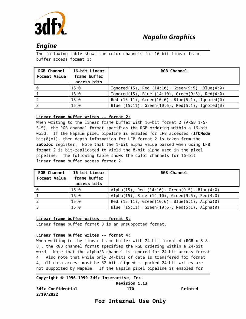
Napalm Graphics Engine Note that the polarity of the VMI Vsync, Hsync, and Vactive signals is programmable. The inactive going edge of the Vsync signal indicated whether the field is odd or even. If Hsync is active during the inactive going edge of Vsync, the field is even. If Hsync is inactive, the field is odd.
11.1.9 3.1.9 vidSerialParallelPort RegisterThe vidSerialParallelPort register controls the chip’s I2C, DDC, GPIO, and the host port interface. Since VMI and ROM share pins for their interface, a pin can be input or output depending on which interface has control of the pin at that time. GPIO[0] is a hardwired output pin designed to be an output enable of the on-board tristate drivers. GPIO[0] is asserted low, when the VMI device has control of the shared pins, and is driving pixdata[7:0], vmi_rdy_n, and vmi_intreq_n as input to Napalm. GPIO[0] is pulled high, when ROM controls the shared pins, and pixdata[7:0], vmi_rdy_n, and vmi_intreq_n are output of Napalm.
Copyright 1996-1999 3dfx Interactive, Inc. Revision 1.133dfx Confidential 170 Printed 5/7/2023
For Internal Use Only
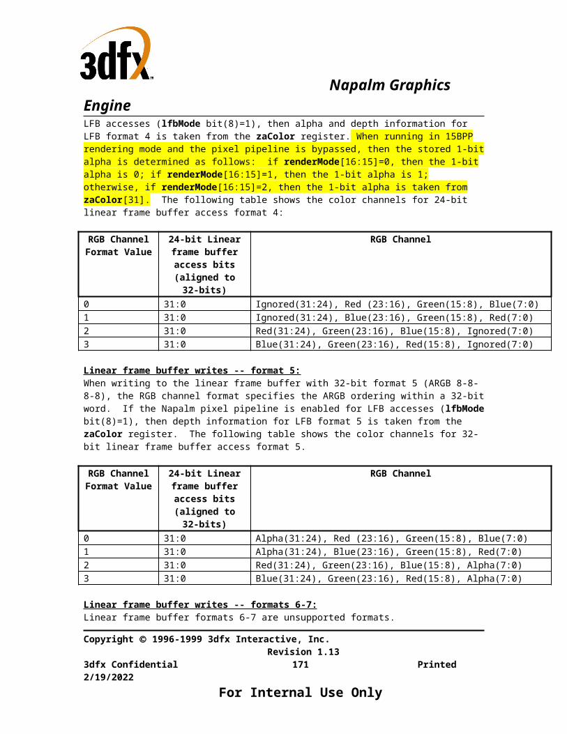
Napalm Graphics Engine GPIO[1] is software programmable, and is used to control the output enable of the on-board tristate drivers for vmi_pixclk, vmi_vsync, vmi_hsync, and vmi_vactive. These are the signals that should be continually driven by the external vmi device even when the ROM is using the shared pins (ROM does not use the vmi_pixclk, vmi_vsync, vmi_hsync, and vmi_vactive pins). Otherwise the internal state of the vmi controller in Napalm may be messed up. Vmi_cs_n cannot be used in lieu of GPIO[1] for this purpose because the chip select pin can be turned off by vmi parallel host interface enable bit (bit 0 below).
Bit Written By Description0 host VMI parallel host interface enable. (0=off, 1=on); Default to 0 upon reset.1 host VMI CS_N (Chip Select)
Mode A Mode B2 host VMI DS_N (Data Strobe) VMI RD_N (Read)3 host VMI RW_N (Read/ Write_n) VMI WR_N (Write)4 VMI VMI data DTACK_N (Data
Acknowledge)VMI data RDY (Data Ready)
5 host VMI Data output enable_n. (0 = enabled, 1 = disabled); Default to 1 upon reset.13:6 host/VMI VMI Data (Input / Output)17:14 host VMI Address
DDC interface18 host DDC port enable (0 = disabled, 1 = enabled) Default to 0 upon reset.19 host DDC DCK write (0 = DCK pin is driven low, 1= DCK pin is tri-stated)
When this pin is tri-stated, other devices can drive this line, and the final state of the pin is reflected in bit 26. Default to 1 upon reset.
20 host DDC DDA write (0 = DDA pin is driven low, 1= DDA pin is tri-stated)When this pin is tri-stated, other devices can drive this line, and the final state of the pin is reflected in bit 27. Default to 1 upon reset.
21 Monitor DDC DCK state (read only, 0 = low, 1 = tri-stated which means no device is driving this pin)
22 Monitor DDC DDA state (read only, 0 = low, 1 = tri-stated which means no device is driving this pin)I2C interface
23 host I2C port enable (0 = disabled, 1 = enabled) Default to 0 upon reset.24 host I2C SCK write (0 = SCK pin is driven low, 1= SCK pin is tri-stated)
When this pin is tri-stated, other devices can drive this line, and the final state of the pin is reflected in bit 21. Default to 1 upon reset.
25 host I2C SDA write (0 = SDA pin is driven low, 1= SDA pin is tri-stated)When this pin is tri-stated, other devices can drive this line, and the final state of the pin is reflected in bit 22. Default to 1 upon reset.
26 VMI/encoder
I2C SCK state (read only, 0 = low, 1 = tri-stated which means no device is driving this pin)
27 VMI/encoder
I2C SDA state (read only, 0 = low, 1 = tri-stated which means no device is driving this pin)Misc.
28 host VMI reset_n (1 = normal. 0 = reset VMI device.) Default to 0 upon reset.29 host output only gpio GPIO[1] output30 VMI/
encoderinput only gpio GPIO[2] input
31 Host TV out reset_n (1 = normal, 0 = reset TV out device). Default to 0 upon reset.
Copyright 1996-1999 3dfx Interactive, Inc. Revision 1.133dfx Confidential 171 Printed 5/7/2023
For Internal Use Only
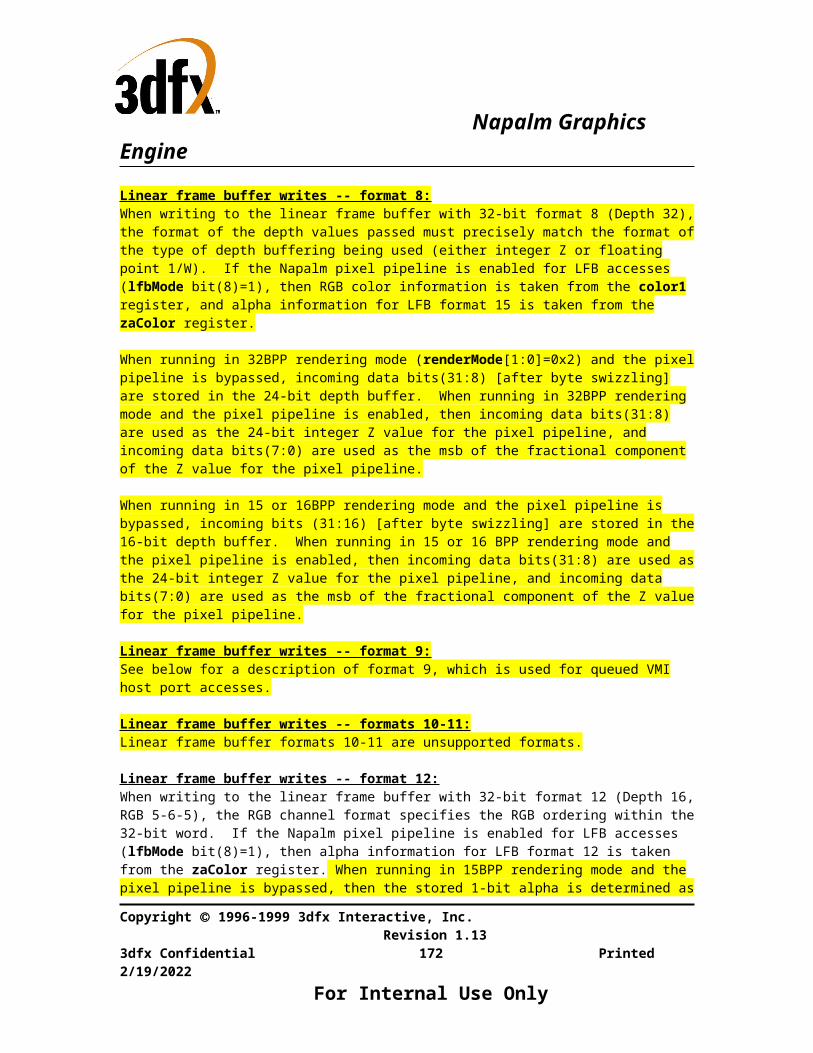
Napalm Graphics Engine VMI and ROM Pin Sharing (see Notes below)
Pin Rom Access VMI AccessName Number Function Type Function TypePixdata/a0 A0 out Y0/Cr0/Cb0* inPixdata/a1 A1 out Y1/Cr1/Cb1* inPixdata/a2 A2 out Y2/Cr2/Cb2* inPixdata/a3 A3 out Y3/Cr3/Cb3* inPixdata/a4 A4 out Y4/Cr4/Cb4* inPixdata/a5 A5 out Y5/Cr5/Cb5* inPixdata/a6 A6 out Y6/Cr6/Cb6* inPixdata/a7 A7 out Y7/Cr7/Cb7* invmi_adr/a8 A8 out vaddr0 outvmi_adr/a9 A9 out vaddr1 outvmi_adr/a10 A10 out vaddr2 outvmi_adr/a11 A11 out vaddr3 outvmi_cs_n CANNOT USE! vmi_cs_n outvmi_rw A14 out vmi_rw_n/
vmi_wr_nout
vmi_ds_n/a15 A15 out vmi_ds_n/vmi_rd_ n
out
vmi_rdy/busy A12 out vmi_dtack_n/vmi_rdy_n*
in
vmi_hdata D0 in/out vmi_hd_0 in/outvmi_hdata D1 in/out vmi_hd_1 in/outvmi_hdata D2 in/out vmi_hd_2 in/outvmi_hdata D3 in/out vmi_hd_3 in/outvmi_hdata D4 in/out vmi_hd_4 in/outvmi_hdata D5 in/out vmi_hd_5 in/outvmi_hdata D6 in/out vmi_hd_6 in/outvmi_hdata D7 in/out vmi_hd_7 in/outHsync NOT USED hsync inVsync NOT USED vsync_n inBlank_n NOT USED blank_n inpix_clk_in NOT USED vid_clk_in invmi_intreq_n A13 out vmi_int_n* invmi_reset_n NOT USED reset_n outrom_oe_n rom_oe_n out CANNOT USE!rom_we_n rom_we_n out CANNOT USE!i2c_clk NOT USED i2c_clk outi2c_data NOT USED i2c_data in/outgp_io[0] vmi_oe_n out vmi_oe_n outgp_io[1] vmi_sync_oe_n out vmi_sync_oe_n outgp_io[2] gp_in in gp_in in* means the signal may be buffered from the VMI data bus to ensure that it is not driven during ROM accesses.
TV Encoder Pins (see Notes below)Pin TV Encoder/Flat Panel
Name Number Function (Scrambled)
Type
Copyright 1996-1999 3dfx Interactive, Inc. Revision 1.133dfx Confidential 172 Printed 5/7/2023
For Internal Use Only

Napalm Graphics Engine
(Unscrambled)rising/falling rising/fallingedge edge
tv_data[0] B0/G1 G3/R7 outtv_data[2] B1/R0 G2/R6 outtv_data[2] B2/R1 G1/R5 outtv_data[3] G0/R2 G0/R4 outtv_data[4] B3/G5 B7/R3 outtv_data[5] B4/G6 B6/R2 outtv_data[6] B5/G7 B5/R1 outtv_data[7] B6/R3 B4/R0 outtv_data[8] B7/R4 B3/G7 outtv_data[9] G2/R5 B2/G6 outtv_data[10] G3/R6 B1/G5 outtv_data[11] G4/R7 B0/G4 outtv_clk_out Clock_out outtv_hsync Hsync in/outtv_vsync Vsync in/outtv_blank Blank_n in/outtv_inclk Clock_in in tv_reset Reset_n out
Notes:1. Rom access and VMI video data/host port access can only be performed separately.2. The Type field in the tables above are referenced to Napalm.3. Programming of the VMI or TV Encoder device can be done via I2C, e.g. setting PAL mode.4. The TV encoder must be able to operate in Master mode where it supplies the clock, vsync, hsync,
blank and Napalm outputs tv_clk_out (delayed version of tv_inclk) and synchronous data.5. We must route a reference board to make sure the pin functions have been shared to provide a decent
route.6. The ROM cs_n is tied to GND, the oe_n and we_n are used to control read/write respectively.
11.1.10 3.1.10 vidTvOutBlankHCount If TV Out Genlock is enabled (VidInFormat[16] == 1’b1, VidInFormat[18]== 1’b1), and Not_use_vga_timing_signal is asserted, vidTvOutBlankHCount bits[10:0] contains the number of clock cycles after the leading edge of tv_hsync before the horizontal active region starts (i.e., horizontal blank becomes deasserted).
vidTvOutBlankHCount bits[26:16] contains the number of clock cycles after leading edge of tv_hsync before the horizontal active region ends (i.e., horizontal blank is re-asserted).
Output blank_n == horizontal blank_n AND vertical blank_n.
Note that the value in bits[26:16] needs to be greater than bits[10:0]. The clock cycles are based on the clock coming in through the tv_inclk pin.
Bit Description10:0 The number of clock cycles after the leading edge of tv_hsync before the horizontal active
region starts (i.e., horizontal blank becomes deasserted).15:11 Reserved
Copyright 1996-1999 3dfx Interactive, Inc. Revision 1.133dfx Confidential 173 Printed 5/7/2023
For Internal Use Only

Napalm Graphics Engine 26:16 The number of clock cycles after leading edge of tv_hsync before the horizontal active
region ends (i.e., horizontal blank is re-asserted).31:27 Reserved
11.1.11 3.1.11 vidInXDecimDeltas (for VMI downscaling Brensenham Engine)/ vidTvOutBlankHCount (for TV out master mode)If VideoIn Interface is configured to VMI mode (i.e., VidInFormat[15:14] == 2’b01), vidInXDecimDeltas bits [11:0] contain the width of the destination video-in surface (width of the video overlay stored in the frame buffer) in number of pixels. VidInXDecimDeltas bits[27:16] contain the width difference between the source video-in surface (from VMI port) and destination video-in surface in number of pixels (Source - Destination)
Bit Description11:0 The positive (unsigned) value added to the error term when the horizontal Bresenham error
term is <0. It is programmed to be the width of the destination video-in surface in number of pixels.
15:12 reserved27:16 The positive (unsigned) value added to the error term when the horizontal Bresenham error
term is >0. It is programmed to be the difference between the width of the source and destination video-in surfaces. (Source - Destination) in number of pixels.
31:28 reserved
11.1.12 3.1.12 vidInDecimInitErrsBit Description12:0 The signed (2’s complement) initial value of the error term in the horizontal
Bresenham accumulator15:13 reserved28:16 The signed (2’s complement) initial value of the error term in the vertical Bresenham
accumulator31:29 reserved
11.1.13 3.1.13 vidInYDecimDeltasIf VideoIn Interface is configured to VMI mode (i.e., VidInFormat[15:14] == 2’b01), vidInYDecimDelta bits[11:0] contain the height of the destination video input window (height of the video overlay stored in the frame buffer) in number of lines. vidInYDecimDeltas contains the height difference between the source video surface (from VMI port) and destination video input window in number of lines (Source - Destination).
Bit Description11:0 The positive value added to the error term when the vertical Bresenham error term is
<015:12 reserved27:16 The positive value added to the error term when the vertical Bresenham error term is
>031:28 reserved
Copyright 1996-1999 3dfx Interactive, Inc. Revision 1.133dfx Confidential 174 Printed 5/7/2023
For Internal Use Only
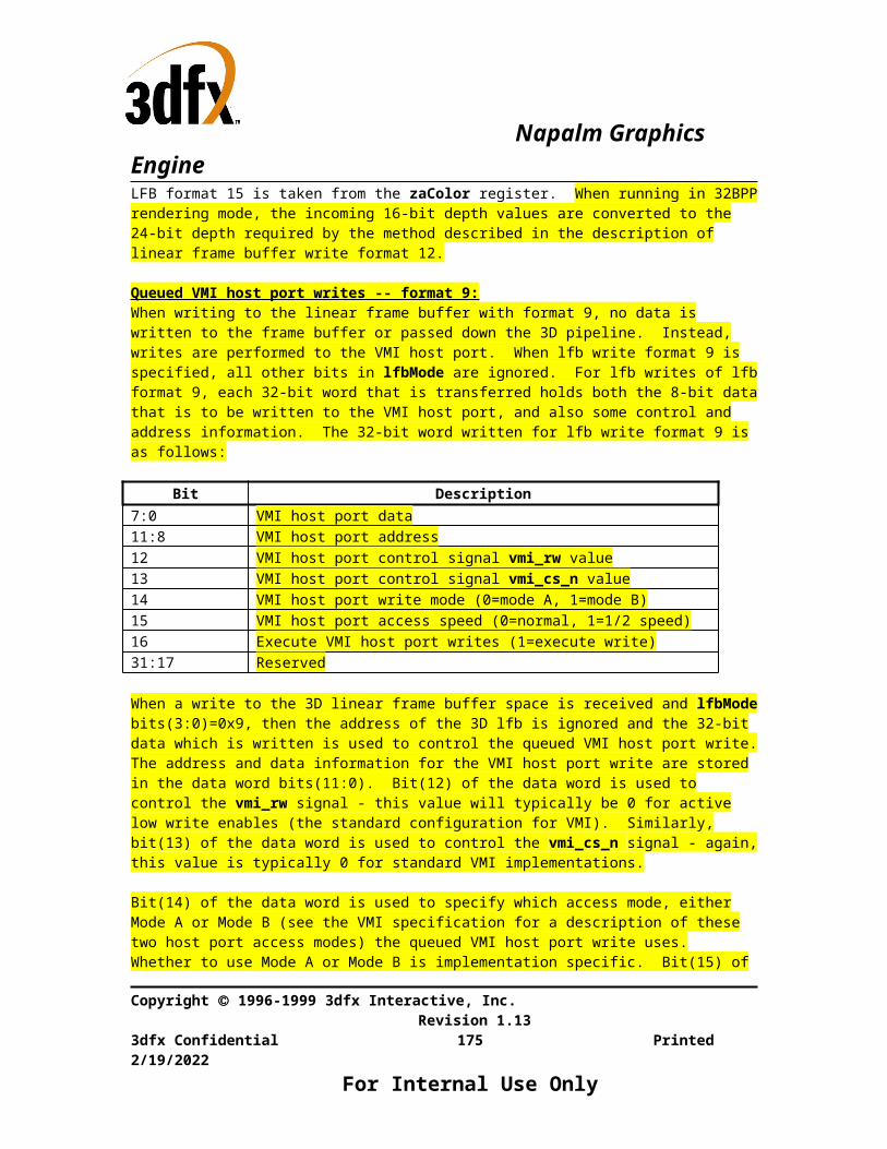
Napalm Graphics Engine Bresenham scaler for scaling down a video window in the horizontal direction:
error = vidInXDecimInitErr;
repeat until the source pixels of a video window scanline are exhausted
if (error < 0)
move to next source pixel
error = error + vidInXDecimDelta1
else
select the current source pixel as the destination pixel
move to next source pixel
error = error - vidInXDecimDelta2
Bresenham scaler for scaling down a video window in the vertical direction:
error = vidInYDecimInitErr
at each VideoIn Hsync
if (error < 0)
skip the whole line of video in data
error = error + vidInYDecimDelta1
else
select the current line of video in data
error = error - vidInYDecimDelta2
11.1.14 3.1.14 vidPixelBufTholdThe vidPixelBufThold determines how many empty slots in each of the three pixel buffers will trigger refilling of the buffers.
Bit Description5:0 Primary pixel buffer low watermark (0x0 – 1 empty slot; 0x3f – 64 empty slots)11:6 Secondary pixel buffer 0 low watermark (0x0 – 1 empty slot; 0x3f – 64 empty slots)17:12 Secondary pixel buffer 1 low watermark (0x0 – 1 empty slot; 0x3f – 64 empty slots)
11.1.15 3.1.15 vidChromaKeyMin RegisterThe vidChromaKeyMin register contains the lower bound of the chroma key color.
Bit Description8-bit desktop color format
7:0 chroma key color31:8 Reserved
15-bit desktop color format4:0 Blue value of the chroma -key
Copyright 1996-1999 3dfx Interactive, Inc. Revision 1.133dfx Confidential 175 Printed 5/7/2023
For Internal Use Only

Napalm Graphics Engine 9:5 Green value of the chroma -key14:10 Red value of the chroma -key31:15 Reserved
16-bit desktop color format4:0 Blue value of the chroma -key10:5 Green value of the chroma -key15:11 Red value of the chroma -key31:16 Reserved
24-bit desktop color format7:0 Blue value of the chroma -key15:8 Green value of the chroma -key23:16 Red value of the chroma -key31:24 Reserved
32-bit desktop color format7:0 Blue value of the chroma -key15:8 Green value of the chroma -key23:16 Red value of the chroma -key31:24 Reserved
11.1.16 3.1.16 vidChromaKeyMax RegisterThe vidChromaKeyMax register contains the upper bound of the chroma key color. It is the same as vidChromaKeyMin if the chroma-key is a single color instead of a range.
Bit Description31:0 Format same as vidChromaKeyMin Register
11.1.17 3.1.17 vidInStatusCurrentLine RegisterThe vidInStatusCurrentLine register contains the current scan out line. As the vertical beam scans down the display this register is incremented.
Bit Description10:0 Current Video scan line.
The vidInStatusCurrentLine register also allows the host to read the status of the video-in port, and implement manual buffer flipping for the video-in data.
Bit Description16 Even/odd field of the frame VMI just finishes drawing. 1=even; 0=odd.18:17 Video-in buffer VMI just finishes writing to.
00=buffer 0 (as specified by vidInAddr0);01=buffer 1 (as specified by vidInAddr1);10=buffer 2 (as specified by vidInAddr2);11=No buffer is ready yet, video processor is still working on the first frame
11.1.18 3.1.18 vidScreenSizeNOTE: Whenever the screen resolution is changed, video processor needs to be re-enabled by clearing vidProcCfg bit 0 and setting it to 1. This will reset the video processor.
Bit Description
Copyright 1996-1999 3dfx Interactive, Inc. Revision 1.133dfx Confidential 176 Printed 5/7/2023
For Internal Use Only

Napalm Graphics Engine 11:0 Width of the screen in number of pixels. If vidScreenX is specified to be bigger than
1280, 2x mode needs to be enabled.22:12 Height of the screen in number of lines.23 desktop_addr_fifo_enable
11.1.19 3.1.19 vidOverlayStartCoordsBit Description11:0 The x-coordinate on the screen where the upper left corner of the overlay locates.23:12 The y-coordinate on the screen where the upper left corner of the overlay locates.25:24 The lower two bits of the x-coordinate for the first pixel (at the upper left corner) of the
overlay window with respect to the beginning of the source surface. Since the overlay window may be partially occluded by the dimension of the screen, the first pixel of the window may not necessarily be the first pixel of the source surface. The lower two bits of the x-coordinate are used for undithering, and are the same for both linear and tiled address space.
27:26 The lower two bits of the y-coordinate for the first pixel (at the upper left corner) of the overlay window with respect to the beginning of the source surface. Since the overlay window may be partially occluded by the dimension of the screen, the first pixel of the window may not necessarily be the first pixel of the source surface. The lower two bits of the y-coordinate are used for undithering, and are the same for both linear and tiled address space.
31:28 reserved
11.1.20 3.1.20 vidOverlayEndScreenCoordBit Description11:0 The x-coordinate on the screen where the lower right corner of the overlay locates.23:12 The y-coordinate on the screen where the lower right corner of the overlay locates.
11.1.21 3.1.21 vidOverlayDudxBit Description19:0 Step size in source per horizontal step in screen space for magnification. Format is
0.20.if enhanced video is enabled, this register is defined to be the number of active pixels of a scanline before the the driver of dac_hsync is switched over from one chip to another. For example, in a 640x480 display, and vidOverlayDuDx is set to 320 (decimal), then the hsync is switch over at the middle of a scanline.
11.1.22 3.1.22 vidOverlayDudxOffsetSrcWidthBit Description18:0 Initial offset of Dudx. Format is 0.19.31:19 Number of bytes needed to be fetched from the source surface in order to cover a
whole un-occluded scanline for the overlay (14 bits allows a max of 16K bytes for an overlay scanline). Note that the msb is located in the bit 31 of vidDesktopOverlayStride reg.i.e., ((Overlay width in number of screen pixels * vidOverlayDudx) + vidOverlayDudxOffset)) * overlay pixel depth in bytes.For non-scaled overlay with no offset, vidOverlayDudx becomes 1, and
Copyright 1996-1999 3dfx Interactive, Inc. Revision 1.133dfx Confidential 177 Printed 5/7/2023
For Internal Use Only

Napalm Graphics Engine
vidOverlayDudxOffset becomes 0 in the above equation.
11.1.23 3.1.23 vidOverlayDvdyBit Description19:0 Step size in source per vertical step in screen space for magnification. Format is 0.20.
11.1.24 3.1.24 vidOverlayDvdyOffsetBit Description18:0 Initial offset of Dvdy. Format is 0.19.
Example:
Given source size of 640 x 240 and have it magnified to 1024 x 768 on the screen.
Source width:Dudx[31:19] = 640 X 2 bytes = 1280 bytes (here 16 bpp assumed)= 500h
Dudx[19:0] = 640/1024 = 0.625 = a0000h(Note format is 0.20 meansx x x x x x x x x x x x x x x x x x x x| | | | | | ......................| | 0.125| || 0.25|0.5)
Dvdy[19:0] = 240/768 = 0.3125 = 0.25 + 0.0625 = 50000h(Format same as dudx above)
Dudx Offset[18:0] and Dvdy Offset [18:0] = 00000h if no initial offset is needed.If upper leftmost overlay pixel needs to be the center ofthe first pixel of the overlay surface, both offsets needs to be set to 0.5which is 40000h.
11.1.25 3.1.25 vidDesktopStartAddrBit Description25:0 Physical starting address of the desktop surface. This is a byte-aligned address.
11.1.26 3.1.26 vidDesktopOverlayStrideBit Description14:0 If the desktop surface resides in linear space, bit[14:0] contains the linear stride of the
surface in bytes. If interlaced video output mode is enabled, the linear stride is still programmed to 1x the regular stride of the surface, and will be multiplied by 2 when used. If the desktop resides in tile space, bit[14:0] contains the tile stride of the region. This
Copyright 1996-1999 3dfx Interactive, Inc. Revision 1.133dfx Confidential 178 Printed 5/7/2023
For Internal Use Only
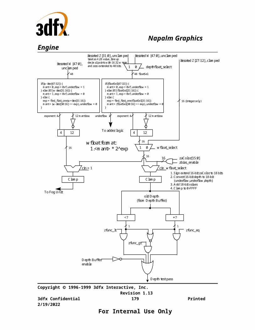
Napalm Graphics Engine
is specified in number of tiles across the width of the tile address region, NOT the width of the desktop surface.
15 Reserved
For video overlay, the stride needs to be a multiple of 4-bytes for YUV 422 pixel format and a multiple of 8-bytes for YUV 411 pixel format. This ensures that the right edge of the video source surface to fall on a boundary of 2 pixels for YUV 422 and 4 pixels for YUV 411. The start address for the overlay is sampled from the FIFO’ed leftOverlayBuf and rightOverlayBuf registers. The start address needs to be aligned on a 32-bit boundary for YUV 422 pixel format and a 64-bit boundary for YUV 411 pixel format.
Bit Description30:16 If the overlay surface resides in linear space, bit[30:16] contains the linear stride of the
overlay surface in bytes. If interlaced video output mode is enabled, the linear stride is still programmed to 1x the regular stride of the surface, and will be multiplied by 2 when used.If the overlay resides in tile space, bit[30:16] contains the tile stride of the region. This is specified in number of tiles across the width of the tile address region, NOT the width of the overlay surface.
31 The msb of vidOverlayDudxOffsetSrcWidth. This bit is used when the number of bytes needed to be fetched for the overlay exceeds 13 bits.
11.1.27 3.1.27 vidInAddr0Bit Description25:0 Starting address of video-in buffer 0
11.1.28 3.1.28 vidInAddr1Bit Description25:0 Starting address of video-in buffer 1
11.1.29 3.1.29 vidInAddr2Bit Description25:0 Starting address of video-in buffer 2
11.1.30 3.1.30 vidInStrideBit Description14:0 If the video-in buffers reside in linear space, this register contains the linear stride of
the buffer in bytes. If interlaced video input mode is enabled, the linear stride is still programmed to 1x the regular stride, and will be multiplied by 2 before used. If the video-in buffers reside in tile space, this register contains the tile stride of the region. This is specified in number of tiles across the width of the tile address region, NOT the width of the video-in buffers.
Copyright 1996-1999 3dfx Interactive, Inc. Revision 1.133dfx Confidential 179 Printed 5/7/2023
For Internal Use Only
Napalm Graphics Engine 11.1.31 3.1.31 vidCurrOverlayStartAddrThe vidCurrOverlayStartAddr register allows the host to read the start address which the video processor is using to refresh the overlay window for the current frame.
Bit Description25:0 Start physical address the video processor is using to refresh the overlay window. Read only.
11.2 3.2 Video-In Interface
11.2.1 3.2.1 FunctionVideo In Processor supports several connector interfaces for video data input. The following table shows the signals needed for each interface.
11.2.2 3.2.2 Signals
Ports DDC(I2C) VMI* VMI (Mode A) VMI (Mode B)VMI Video Port Hsync in Hsync in Hsync inVMI Video Port Vsync in Vsync in Vsync inVMI Video Port Vactive Vactive VactiveVMI Video Port P[7:0] P[7:0] P[7:0]VMI Video Port Pixclk (in) Pixclk (in) Pixclk in)VMI I2C Port SDA (in/out)VMI I2C Port SCK (in/out)VMI Host Port D[7:0] (in/out) D[7:0]VMI Host Port A[3:0] (out) A[3:0]VMI Host Port cs_n (out) cs_nVMI Host Port ds_n (out) rd_nVMI Host Port r/w_n (out) wr_nVMI Host Port dtack_n (in) readyDDC Port SDA (in/out)DDC Port SCK (in/out)System signals vmi_reset_n (out) vmi_reset_n (out) vmi_reset_n (out)System signals vmi_int_n (in) vmi_int_n vmi_int_nSystem signals vmi_present_n (in) vmi_present_n vmi_present_n
A. Video-In Interface:
General Description
When video data arrives through the Video-In interface, they undergo the optional decimation and filtering, packed into words of 128 bits in a FIFO before written into the memory. As writes to the memory is always aligned on a 128-bit boundary, the appropriate byte enables also need to be set with the writes. Supported pixel formats for the video-in data are YUV422 and YUV411. Both pixel formats are stored in a form of 16 bit per pixel, which means that 4 bit are unused per pixel in the case of YUV411.
Video data are stored in the Video-In frame buffers whose starting addresses are specified by the registers VidInAddr0, VidInAddr1, and VidInAddr2. VidInAddr1 and VidInAddr2 are used for double and triple buffering to avoid video tearing. However, since video is coming in at a different rate from the video
Copyright 1996-1999 3dfx Interactive, Inc. Revision 1.133dfx Confidential 180 Printed 5/7/2023
For Internal Use Only
Napalm Graphics Engine refresh, switching of the video-in drawing buffers is not synchronous to the Vsync of the video refresh. At the end of each VMI frame, the vmi_int input signal will be asserted. The video processor will then switch to the next video-in frame buffer for the next VMI frame if multiple buffering is enabled. If disabled, the same video-in frame buffer will be overwritten. At the same time, the video processor also updates the VidInStatus register which indicates the VMI buffer VMI just finishes drawing (0, 1, 2), and whether the buffer contains even or odd field. An interrupt signal will signal the host for display buffer flipping for the video-in data. On the other hand, if the “Video_in data displayed as overlay enable” bit in VidProcCfg is set, the video porcessor will do the display buffer flipping automatically for the overlay provided that all the corresponding configuration registers for the overlay is set up correctly (e.g., overlay surface enable, overlay pixel format, overlay_dudx, …… etc).
If Weave video-in deinterlaced mode is enabled, the video processor detects even/odd field from VREF(Vsync) and HREF(Hsync). If odd, the specified VidInAddr register will be used as the starting address of the video-in frame buffer. If even, VidInStride will be used as the starting address offset, and added to the specified VidInAddr. Video-in buffer will be switched at every other Vsync. VidInStride should be programmed to contain the a value which equals to 1X the regular line stride regardless of whether the video-in data is interlaced or not.
1. VMI
-data:
8-bit YCbCr interface is used. The data format is CCIR-656 YCbCr 422, and pixels arrive in the style of (Cb0[7:0] or U0[7:0]) -> Y0[7:0] -> (Cr0[7:0] or V0[7:0]) -> Y1[7:0].
Video data may be interlaced.
-timing:
Timing signals include VREF, HREF, VACTIVE, and PIXCLOCK.
VREF and HREF are active high VSYNC and HSYNC. If HREF is high during the falling edge of VREF, the field is even. If HREF is low at that time, the field is odd.
VACTIVE is a blanking signal which indicates pixel data is valid across the YCbCr bus.
11.3 3.3 Video Limitation
1. In 1x mode, 3 streams of pixel fetching will consume more memory bandwidth than available for 32-bit desktop. This means chroma-keying and bilinear filtering cannot be turned on simultaneously for 32-bit desktop.
2. In 2x mode (for any display larger than 1280 X 1024) where we refresh 2 screen pixels per cycle at 110MHz, bilinear filtering is not supported. All backend zoom (magnification) is done by point sampling (replication).
3. 1 - 10X backend zoom (magnification) with increments of 0.1X. Larger magnification is supported, but with bigger increments.
1 to 1/16X video-in decimation (minimization) with increments of 0.015X.
4. Retain the 3-bit tap filter for RGB565 dithered as an alternative to the 2x2 box filter.
Copyright 1996-1999 3dfx Interactive, Inc. Revision 1.133dfx Confidential 181 Printed 5/7/2023
For Internal Use Only
Napalm Graphics Engine
5. Interlaced video output mode is not implemented.
6. Hw cursor is 2 color only.7. YUV 411 pixel format will be stored as unpacked in the frame buffer. This means each pixel
will occupy 16 bits instead of 12 bits. This makes pixel extraction easier, but consumes more memory.
8. Video with YUV 422 format needs to be stored on a 4-byte memory boundary while YUV 411 on a 8-byte boundary. This is necessary because UV are shared between 2 pixels in 422 while UV are shared between 4 pixels in 411.
12.
13. Command Transport Protocol
13.1 Command TransportA command FIFO (CMDFIFO) may be established by software within frame buffer memory or AGP memory. Writes to the linear frame buffer address space are performed to build a command buffer, which is then parsed and executed by the accelerator. To accommodate host CPUs which may issue writes out-of-order (eg. Intel’s Pentium Pro), one of two scenarios will occur, the CMDFIFO resides in AGP (non-local video memory) and software manages the accelerator’s internal CMDFIFO depth register, or the CMDFIFO resides in frame buffer memory and the accelerator manages the internal CMDFIFO depth register.
If the CMDFIFO resides in AGP space (non-local video memory), software “BUMPS” the internal CMDFIFO depth register after N words into the AGP buffer. This allows the CPU to write to the CMDFIFO in any order, flush any pending writes in the CPU’s internal write buffers and core logic chipset’s internal write buffers, then update the accelerator’s depth register. Since writes to the CMDFIFO will be in consecutive order, the CPU’s write buffers will fill and burst into memory more efficiently, than random PCI writes.
If the CMDFIFO resides in frame buffer memory, software writes to the frame buffer in consecutive order, the CPU flushes its write buffer in any order to the accelerator. The accelerator counts the number of non written addresses, once consecutive addresses are written, the internal CMDFIFO depth register is updated to the last consecutive written address. Counting unwritten addresses allows the CPU to flush its internal write buffers in any order, but maintains the correct order in the frame buffer memory. Software must manage the circular buffer at the point where the buffer recycles to the beginning. This is done by placing a JMP instruction (CMDFIFO Packet Type 0, Func 100) at the bottom of the fifo to restart at the beginning of the CMDFIFO space.
Copyright 1996-1999 3dfx Interactive, Inc. Revision 1.133dfx Confidential 182 Printed 5/7/2023
For Internal Use Only

Napalm Graphics Engine 13.1.1 CMDFIFO ManagementThe CMDFIFO mechanism supports 2 types of fifo management, software and hardware. When the CMDFIFO is located in frame buffer memory either software management or hardware management can be used on the CMDFIFO, unlike AGP which only supports software management of the CMDFIFO.
13.1.1.1 Software Management of CMDFIFOSoftware manages the CMDFIFO “emptiness.” The accelerator maintains a read pointer and a depth for the CMDFIFO. Accelerator reads from the CMDFIFO decrement the depth register and increment the read pointer. The accelerator will automatically execute data from the CMDFIFO as long as the internal CMDFIFO depth register is greater than zero. When the CPU is ready to inform the accelerator that more data is available in the CMDFIFO, the CPU writes the number of 32-bit words that have been added to the end of the CMDFIFO. The accelerator then adds the value written by the CPU to the internal depth register. The accelerator’s internal registers define where the circular CMDFIFO exists in frame buffer memory by defining a beginning address for the CMDFIFO and a rollover address. By default, the CMDFIFO internal read pointer is set to the beginning address for the CMDFIFO. Once data is stored in the CMDFIFO (and the internal depth register is incremented by the CPU), the CMDFIFO read pointer will increment as the accelerator parses and executes the CMDFIFO. When the read pointer equals the rollover address defined by initialization registers, the read pointer will jump back to the beginning CMDFIFO address. The CMDFIFO is thus programmable in size as a circular space from 1 to N 4k byte pages. Software must manage CMDFIFO “fullness” and guarantee that the CMDFIFO does not overflow. On systems like the Intel Pentium Pro, software must place a fence after the last memory write, but before the write to increase the number of new entries in the CMDFIFO.
Copyright 1996-1999 3dfx Interactive, Inc. Revision 1.133dfx Confidential 183 Printed 5/7/2023
For Internal Use Only
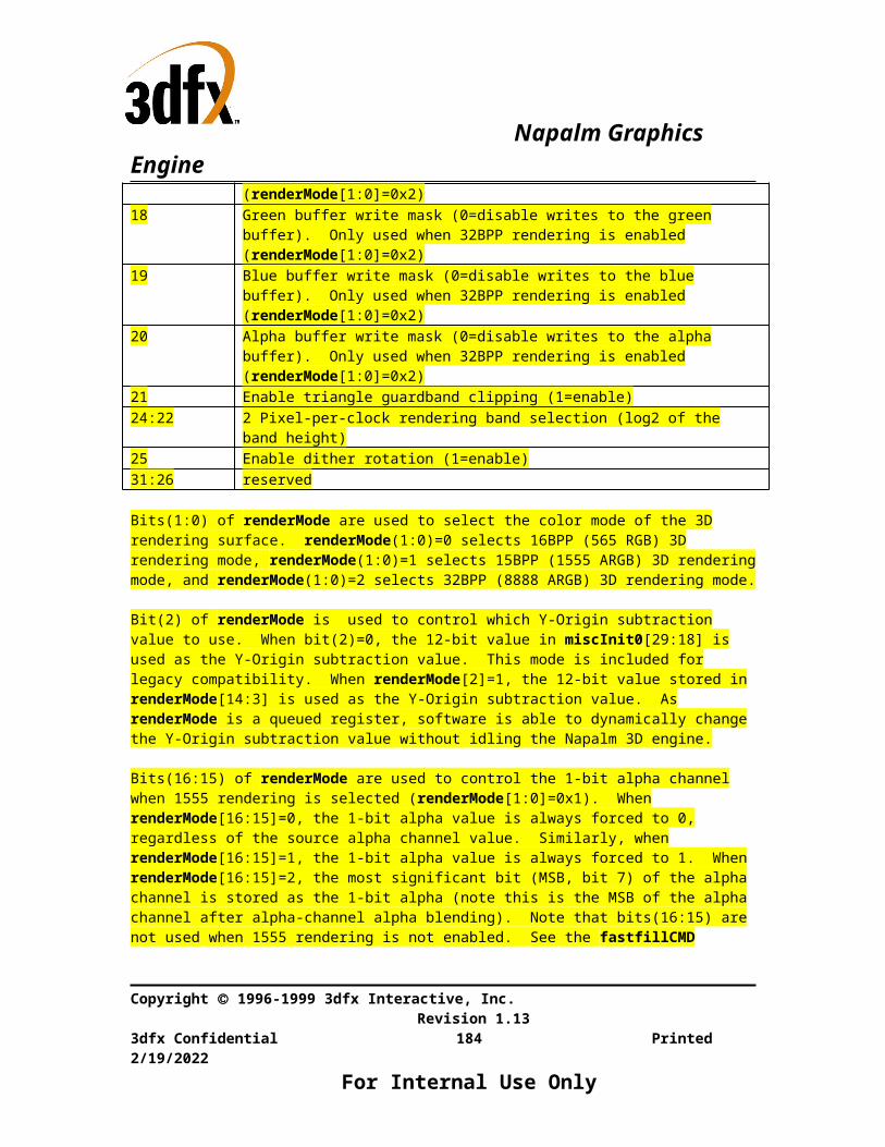
Napalm Graphics Engine 13.1.1.2 Hardware Management of CMDFIFOHardware manages the CMDFIFO “emptiness.” The accelerator maintains a read pointer, write pointer, and depth for the CMDFIFO. Accelerator reads from the CMDFIFO decrement the depth register and increment the read pointer. The accelerator will automatically execute data from the CMDFIFO as long as the internal CMDFIFO depth register is greater than zero. The CPU writes data into the CMDFIFO area in sequential addresses. The accelerator snoops the writes into the CMDFIFO area and examines the addresses, looking for non sequential addresses or “holes.” When the accelerator gathers sequential addresses present in the CMDFIFO, the depth and write pointers are incremented. The accelerator’s internal registers define where the circular CMDFIFO exists in frame buffer memory by defining a beginning address for the CMDFIFO and a rollover address. By default, the CMDFIFO internal read pointer is set to the beginning address for the CMDFIFO. Once data is stored in the CMDFIFO (and the internal depth register is incremented by the CPU), the CMDFIFO read pointer will increment as the accelerator parses and executes the CMDFIFO. When the read pointer equals the rollover address defined by initialization registers, the read pointer will jump back to the beginning CMDFIFO address. The CMDFIFO is thus programmable in size as a circular space from 1 to N 4k byte pages. Software must manage CMDFIFO “fullness” and guarantee that the CMDFIFO does not overflow. On systems like the Intel Pentium Pro, software must place a fence after the last memory write, but before the first write to the top of the CMDFIFO. Software may not write less than four 32 bit entries before performing a jump to the begining of the buffer.
13.1.2 CMDFIFO DataAll CMDFIFO data packets begin with a 32-bit packet header which defines the data which follows. There are 6 different types of CMDFIFO packet headers. Bits (2:0) of a CMDFIFO packet header define the packet header type. All CMDFIFO packet headers and data must be 32-bit words - byte and 16-bit short writes are not allowed in the CMDFIFO.
13.1.3 CMDFIFO Packet Type 0CMDFIFO Packet Type 0 is a variable length packet, requiring a minimum single 32-bit word, to a maximum of 2 32-bit words. CMDFIFO Packet Type 0 is used to jump to the beginning of the fifo when the end of the fifo is reached. CMDFIFO Packet Type 0 also supports jumping to a secondary command stream just like a jump subroutine call (jsr instruction), with a CMDFIFO Packet that instructs a return as well. NOP, JSR, RET, and JMP LOCAL FRAME BUFFER functions only require a single 32-bit word CMDFIFO packet, while the JMP AGP function requires a two 32-bit word CMDFIFO packet. Bits 31:29 are reserved and must be written with 0.
CMDFIFO Packet Type 031 29 28 6 5 3 2 0
word 0 Reserv Address [24:2] Func 000word 1 Reserved Address [35:25]
Code Function000 NOP001 JSR010 RET011 JMP LOCAL FRAME BUFFER
Copyright 1996-1999 3dfx Interactive, Inc. Revision 1.133dfx Confidential 184 Printed 5/7/2023
For Internal Use Only
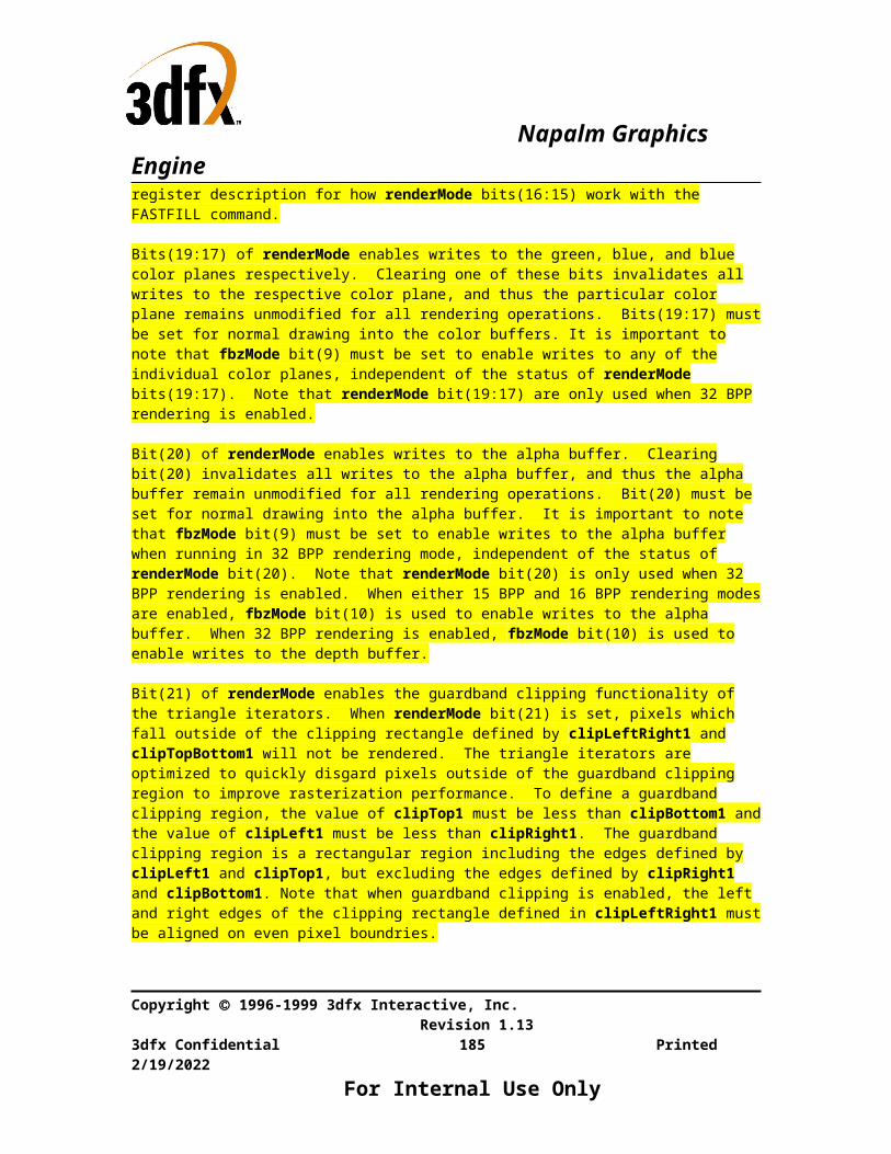
Napalm Graphics Engine
100 JMP AGP
13.1.4 CMDFIFO Packet Type 1CMDFIFO Packet Type 1 is a variable length packet that allows writes to either a common address, or to consecutive addresses, minimum number of words is 2 32-bit words, and maximum number of words is 65536 words. Bits 31:16 define the number of words that follow word 0 of packet type 1, and must be greater than 0. When bit 15 is a 1, data following word 0 in the packet is written in consecutive addresses starting from the register base address defined in bits 14:3. When bit 15 is a 0, data following word 0 is written to the base address. Packet header bits 14:3 define the base address of the packet, see section below. The common use of packet type 1 is host blits.
CMDFIFO Packet Type 131 16 15 14 3 2 0
word 0 Number of words Incc
Register Base (See below) 001word 1 Dataword N Optional Data N
Register base:
Napalm
11 10 8
7 0 02D/3D Chip field Register Number
Bit 11 denotes either 2D or 3D, when set register Number is a 2D number, otherwise Register number is a 3D register.
13.1.5 CMDFIFO Packet Type 2CMDFIFO Packet Type 2 is a variable length packet, requiring a minimum of 2 32-bit words, and a maximum of 30 32-bit words for the complete packet. The base address for CMDFIFO Packet Type 2 is defined to be offset 8 of the hardware 2D registers(clip0min). The first 32-bit word of the packet defines individual write enables for up to 29 data words to follow. From LSB o MSB of the mask, a “1” enables the write and a “0” disables the write. The sequence of up to 29 32-bit data words following the mask modify addresses equal to the implied base address plus N where mask[N] equals “1” as N ranges from 0 to 28. The total number of 32-bit data words following the mask is equal to the number of “1”s in the mask. The register mask must not be 0.
CMDFIFO Packet Type 231 3 2 0
word 0 2D Register mask 010word 1 Dataword N Optional Data N
13.1.6 CMDFIFO Packet Type 3CMDFIFO Packet Type 3 is a variable length packet, requiring a minimum of 3 32-bit words, and a maximum of 16 vertex data groups, where a data group is all the register writes specified in the parameter mask, for the complete packet. It is a requirement that bits 9:6 must be greater than 0. The base address for CMDFIFO Packet Type 3 is defined to be the starting address of the hardware triangle Copyright 1996-1999 3dfx Interactive, Inc. Revision 1.133dfx Confidential 185 Printed 5/7/2023
For Internal Use Only

Napalm Graphics Engine setup registers. The first 32-bit word of the packet defines 16 individual vertex data. Bits 31:29 of word 0 define 0 to 7 dummy fifo entries following the packet type 3 data. The sSetupMode register is written with the data in bits 27:10 of word 0. Bits 9:6 define the number of vertex writes contained in the packet, where the total packet size becomes what is defined in the parameter mask multiplied by the number of vertices. During parsing and execution of a CMDFIFO Packet Type 3, a specific action takes place based on bits 5:3. The sSetupMode register implies that X and Y are present in words 1 and 2. When Bit 28 when set, packed color data follows the X and Y values, otherwise independent red, green, blue, and alpha follow X and Y data. When Smode field is 0, then word 0 defines X, and word 1 defines Y.
Code 000 specifies an independent triangle packet, where an implied sBeginTriCMD is written after 2 sDrawTriCMD’s. The sequence would follow, sBeginTriCMD, sDrawTriCMD, sDrawTriCMD, sBeginTriCMD, until “NumVertex” vertices has been executed.
Code 001 specifies the beginning of a triangle strip, an implicit write to sBeginTriCMD is issued, followed by Num Vertex sDrawTriCMD writes. The sequence would follow, sBeginTriCMD, sDrawTriCMD, sDrawTriCMD, sDrawTriCMD, until “num Vertex” vertices has been executed
Code 010 specifies the a continuance of an existing triangle strip, an implicit write to sDrawTriCMD is performed after one complete vertex has been parsed.
CMDFIFO Packet Type 331 29 28 27 22 21 10 9 6 5 3 2 0
word 0 Num PC SMode Parameter Mask Num Vertex CMD 011word 1 Dataword N Optional Data N
Code Command000 Independent Triangle001 Start new triangle strip010 Continue existing triangle strip 011 reserved1xx reserved
Bit sParamMask field description10 Setup Red, Green, and Blue11 Setup Alpha12 Setup Z13 Setup Wb14 Setup W015 Setup S0 and T016 Setup W117 Setup S1 and T1
sSetupMode field22 Strip mode (0=strip, 1=fan)23 Enable Culling (0=disable,
1=enable)24 Culling Sign (0=positive sign,
1=negative sign)
Copyright 1996-1999 3dfx Interactive, Inc. Revision 1.133dfx Confidential 186 Printed 5/7/2023
For Internal Use Only

Napalm Graphics Engine
25 Disable ping pong sign correction during triangle strips (0=normal, 1=disable)
Parameterword 1 Xword 2 Yword 3 Red / Packed ARGB (optional)word 4 Green (optional)word 5 Blue (optional)word 6 Alpha (optional)word 7 Z (optional)word 8 Wbroadcast (optional)word 9 W0 Tmu 0 & Tmu1 W (optional)word 10 S0 Tmu0 & Tmu1 S (optional)word 11 T0 Tmu0 & Tmu1 T (optional)word 12 W1 Tmu 1 W (optional)word 13 S1 Tmu1 S (optional)word 14 T1 Tmu1 T (optional)
Sequence of implied commands for Each code follows:
M = Mode register write
B = sBeginTriCMD
D = sDrawTriCMD
Code 000: MBDDBDDBDDBDD …
Code 001: MBDDDDDDDDDDD …
Code 010: MDDDDDDDDDDDD …
13.1.7 CMDFIFO Packet Type 4CMDFIFO Packet Type 4 is a variable length packet, requiring a minimum of 2 32-bit words, and a maximum of 22 32-bit words for the complete packet. The first 3 bits 31:29 of word 0 define the number of pad words that follow the packet type 4 data. The next 14 bits of the header 28:15 define the register write mask, followed by the register base field, described later in this section. From LSB to MSB of the mask, a “1” enables the write and a “0” disables the write. The sequence of up to 22 32-bit data words following the mask modify addresses equal to the implied base address plus N where mask[N] equals “1” as N ranges from 0 to 16. The total number of 32-bit data words following the mask is equal to the number of “1”s in the mask. As a requirement, the general register mask must have a non zero value
CMDFIFO Packet Type 431 29 28 15 14 3 2 0
word 0 num General Register mask Register Base (See below) 100word 1 Data
Copyright 1996-1999 3dfx Interactive, Inc. Revision 1.133dfx Confidential 187 Printed 5/7/2023
For Internal Use Only
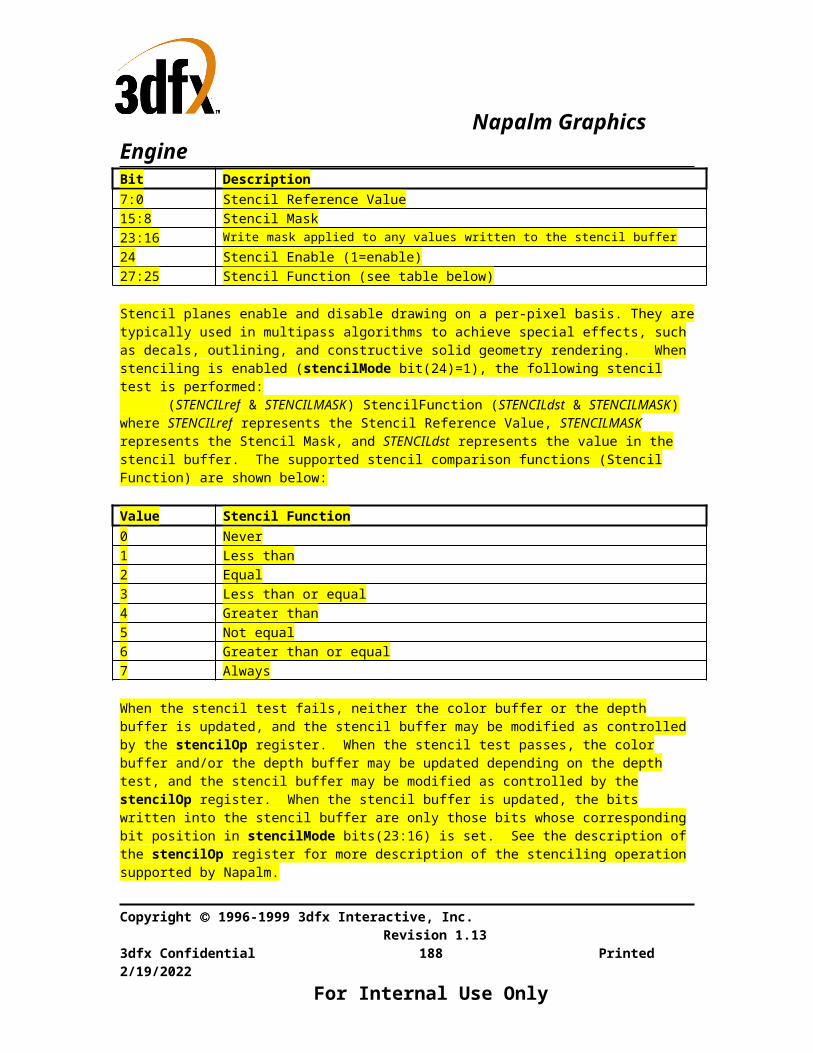
Napalm Graphics Engine
word N Optional Data N
Register base:
Napalm
11 10 8
7 02D/3D Chip field Register Number
Bit 11 denotes either 2D or 3D, when set register Number is a 2D number, otherwise Register number is a 3D register.
13.1.8 CMDFIFO Packet Type 5CMDFIFO Packet Type 5 is a variable length packet, requiring a minimum of 3 32-bit words, and a maximum of 2^19 32-bit words for the complete packet Bits 31:30 define LFB type, one of linear frame buffer, planar YUV space, 3D LFB, or texture download space. Bits 29:26 in word 0 define the byte enables for word 2, and are active low true. Bits 25:22 in word 0 define the byte enables for word N. Data must be in the correct data lane, and the base address must be 32-bit aligned. CMDFIFO Packet Type 5 is used to transfer large consecutive quantities of data from the CPU to the accelerator’s frame buffer with proper order with the command stream. One note, transfer to tile space is limited if tile-stride does not match PCI stride. Tile space rows are not continuous, thus each tile row must be separated into separate packets.
NOTE: when downloading into the texture download space, the aperture is 4MB wide. The lower 2M of this space is sent into the TMU0 download port, while the upper 2M is sent to the TMU1 download port. Downloads to either TMU are not guaranteed to be synchronous with each other. Please refer to the “maintaining texture cache coherency” section of this spec.
Downloads to the TMU0 alias should have a BaseAddress[26:0] starting at 0x000000, while downloads to TMU1 should have a BaseAddress[26:0] of 0x200000. When the hardware receives a CMDFIFO Packet 5 command to download into texture space, the value 0x600000 is added to the downloads generated in order to normalize the downloads to Napalm Address Space. Downloads to the new 64M TMU download port should have a BaseAddress[26:0] starting at (0x4000000 - 0x600000)=0x3a00000.
CMDFIFO Packet Type 5 31 30 29 26 25 22 21
32 0
word 0 Space Byte Enable W2 Byte Enable WN Num Words 101word 1 reserv BaseAddress [26:0]word 2 Dataword N Optional Data N
Code Space00 Linear FB01 Planar YUV10 3D LFB11 Texture Port
Copyright 1996-1999 3dfx Interactive, Inc. Revision 1.133dfx Confidential 188 Printed 5/7/2023
For Internal Use Only

Napalm Graphics Engine 13.1.9 CMDFIFO Packet Type 6CMDFIFO Packet Type 6 is a fixed length packet requiring 5 32-bit words for the complete packet. CMDFIFO Packet Type 6 is primarily used to transfer data from system AGP memory into frame buffer local memory. Bits 20:5 of word 0 define the transfer size in bytes of an AGP transfer. Bits 4:3 define the destination memory space LFB, Planar YUV, 3D LFB, and texture port. Word 1 bits 31:0, and word 2 bits 27:24 define the source system AGP address of the data move. Bits 23:12 define the stride, and bits 11:0 define the width of the source surface in AGP memory. Word 3 defines the destination frame buffer address, while word 4 bits 14:0 define the stride of the destination surface. Note that a bug in the logic in Napalm limits the use of CMDFIFO Packet Type 6 to frame buffer CMDFIFOs only – AGP CMDFIFOs cannot use CMDFIFO Type 6 packets.
CMDFIFO Packet Type 631 26 25
54 3
2 0word 0 reserved Number of transfer bytes [19:0] type 110word 1 AGP[31:0]word 2 AGP[35:32] AGP stride [13:0] width [13:0]word 3 reserve
dFrame buffer offset [26:0]
word 4 reseved Destination stride [14:0]
type Space00 Linear FB01 Planar YUV10 3D LFB11 Texture Port
13.1.10 MiscellaneousNapalm supports two full CMDFIFO streams and each individually can be located in frame buffer memory or AGP space. Each CMDFIFO has it’s own base address register set, that define the starting address, memory space, and size of the CMDFIFO. The CMDFIFO registers contain a write only bump register that increments the write pointer by the amount written to the cmdBump register. Each CMDFIFO contains a read pointer, write pointer, and freespace count of the fifo itself, so the CPU can monitor the progress and fullness of the CMDFIFO. Ordering between the two CMDFIFO’s is first come, first served.
14. AGP/CMD Transfer/Misc Registers Memory Base 0: Offset 0x0080000
Register Name Address Bits R/W DescriptionAGP
agpReqSize 0x000(0) 19:0 R/W Size of AGP requestagpHostAddressLow 0x004(4) 31:0 R/W Host address bits 31:0
Copyright 1996-1999 3dfx Interactive, Inc. Revision 1.133dfx Confidential 189 Printed 5/7/2023
For Internal Use Only
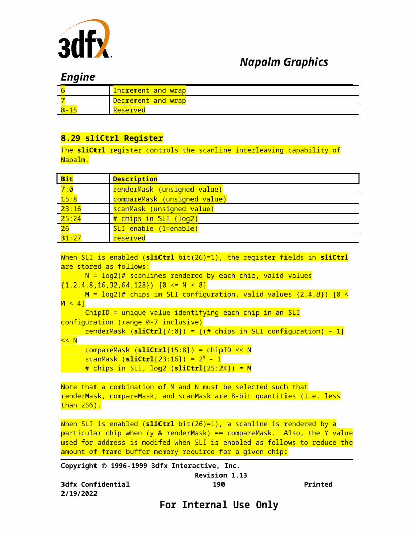
Napalm Graphics Engine agpHostAddressHigh 0x008(8) 31:0 R/W Host address bits 35:32agpGraphicsAddress 0x00C(12) 26:0 R/W Graphics address bits 26:0agpGraphicsStride 0x010(16) 14:0 R/W Graphics strideagpMoveCMD 0x014(20) n/a W Begin AGP transaction
CMDFIFO 0cmdBaseAddr0 0x020(32) 23:0 R/W Base Address of CMDFIFO 0cmdBaseSize0 0x024(36) 10:0 R/W CMDFIFO0 sizecmdBump0 0x028(40) 15:0 W Bump CMDFIFO 0 N wordscmdRdPtrL0 0x02c(44) 31:0 R/W CMDFIFO 0 read pointer lower 32 bitscmdRdPtrH0 0x030(48) 3:0 R/W CMDFIFO 0 read pointer upper 4 bitscmdAMin0 0x034(52) 24:0 R/W CMDFIFO 0 address min pointer
0x038 ReservedcmdAMax0 0x03c(60) 24:0 R/W CMDFIFO 0 address max pointercmdStatus0 0x040(64) 31:0 R Status register (debug & fault coverage)cmdFifoDepth0 0x044(68) 19:0 R/W CMDFIFO 0 depth valuecmdHoleCnt0 0x048(72) 15:0 R/W CMDFIFO 0 outstanding CPU writes
CMDFIFO 1cmdBaseAddr1 0x050(80) 23:0 R/W Base Address of CMDFIFO 1cmdBaseSize1 0x054(84) 10:0 R/W CMDFIFO1 sizecmdBump1 0x058(88) 15:0 W Bump CMDFIFO 1 N wordscmdRdPtrL1 0x05c(92) 31:0 R/W CMDFIFO 1 read pointer lower 32 bitscmdRdPtrH1 0x060(96) 3:0 R/W CMDFIFO 1 read pointer upper 4 bitscmdAMin1 0x064(100) 24:0 R/W CMDFIFO 1 address min pointer
0x068(104) ReservedcmdAMax1 0x06c(108) 24:0 R/W CMDFIFO 1 address max pointercmdStatus1 0x070(112) 31:0 R Status register (debug & fault coverage)cmdFifoDepth1 0x074(116) 19:0 R/W CMDFIFO 1 freespacecmdHoleCnt1 0x078(120) 15:0 R/W CMDFIFO 1 outstanding CPU writes
cmdFifoThresh 0x080(96) 11:0 R/W CMDFIFO fetch thresholdcmdHoleInt 0x084(100) 22:0 R/W Cmd hole timeout value
MiscyuvBaseAddress 0x100(256) 25:0 R/W YUV planar base addressyuvStride 0x104(260) 12:0 R/W Y, U and V planes stride value
14.1 agpReqSizeagpReqSize defines the AGP packet transfer size. The maximum transfer size is 1-Mbyte block of data. This register is read write and defaults to 0x0.
Bit Description19:0 Size, in byte, of AGP packet transfer size. Default is 0x0.
14.2 agpHostAddressLowDuring AGP transfers this address defines the source address bits 31:0 of AGP memory to fetch data from. AGP addresses are 36-bits in length and are byte aligned. The upper 4 bits reside in the agpHostAddressHigh register. This register is read write, and defaults to 0.
Copyright 1996-1999 3dfx Interactive, Inc. Revision 1.133dfx Confidential 190 Printed 5/7/2023
For Internal Use Only
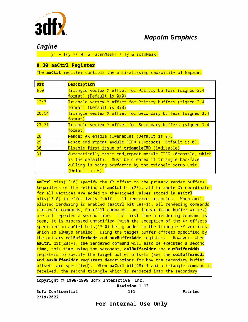
Napalm Graphics Engine Bit Description31:0 Lower 32 bits of AGP memory. Default is 0x0.
14.3 agpHostAddressHighThe agpHostAddressHigh defines the stride, width, and upper 4-bits of source AGP address, during AGP transfers. Stride and width are defined in quadwords. This register is read write, and defaults to 0.
Bit Description13:0 AGP Width. Default is 0x0.27:14 AGP Stride. Default is 0x0.31:28 Upper 4 bits of AGP memory. Default is 0x0.
14.4 agpGraphicsAddress agpgraphicsAddress defines the destination frame buffer address and type of the AGP transfer. At the beginning of an AGP transfer this address is loaded into an internal address pointer that increments for each data received over AGP. This register is read write, and defaults to 0.
Bit Description26:0 Frame buffer offset. Default is 0x0.
14.5 agpGraphicsStrideagpGraphicsStride defines the destination stride in bytes of the AGP transfer. Stride is in multiples of bytes. This register is read write, and defaults to 0.
Bit Description14:0 Frame buffer Stride. Default is 0x0.
14.6 agpMoveCMDagpMoveCMD starts an AGP transfer. When started agpHostAddress is loaded into the source pointer and agpGraphicsAddress is loaded into the destination pointer. The source pointer is incremented after data is fetched from AGP memory and written into frame buffer memory addresses by the destination pointer. The destination pointer is then incremented after the data has been written. This register is write only and has no default.
Copyright 1996-1999 3dfx Interactive, Inc. Revision 1.133dfx Confidential 191 Printed 5/7/2023
For Internal Use Only
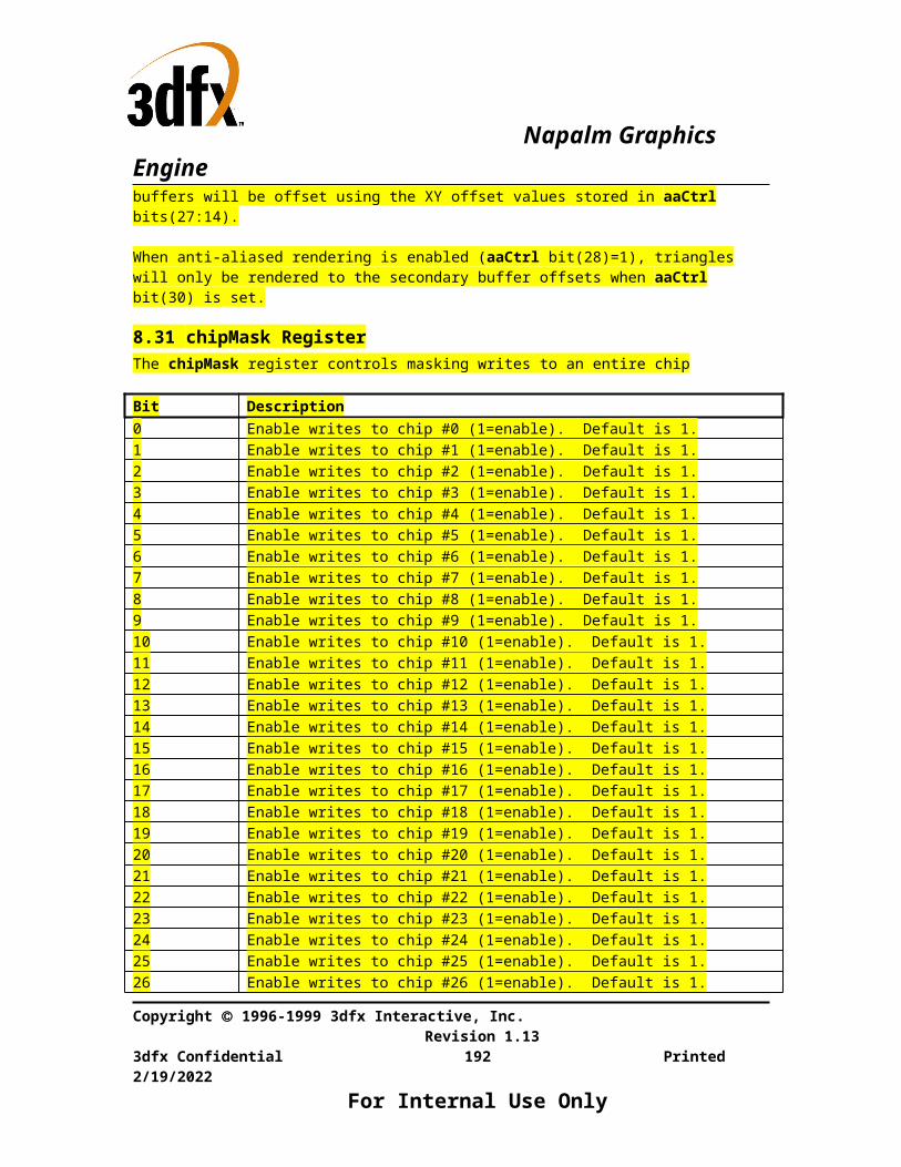
Napalm Graphics Engine
Bit Description2:0 Reserved4:3 Dest memory type (0=Linear FB, 1=planar YUV, 2=3D LFB, 3 = texture port).
Default is 0x0.5 Command stream ID. This bit defines which command fifo when using a host initiated
AGP data move. Default is 0x0.
15. Command Fifo Registers
rdptr
amin
amax
written location unwritten location
Linear Memory Contents
base
addr
The command registers define the location, size, and fifo management method of the command fifo. The command fifo starts at the address defined in the cmdBaseAddr[01] register and occupies N 4k byte pages defined in the cmdBaseSize register. The command fifo can be located either in AGP or frame buffer memory which is defined in the cmdBaseSize register. CmdRdPtr points to the last executed entry in the command fifo. Amin is a pointer that walks through the fifo until it reaches an unwritten location. The rdptr can not access any entry beyond the amin pointer. The amax pointer is set to the furthest address location of a given write. The hole counter is basically the number of unwritten locations between the amax register and the amin register. When the hole counter is zero, the amin register is set to the value of the amax register, thus allowing the read pointer to advance to the new amin register value. The depth of the fifo is calculated by the difference between amax and rdptr.
15.1 cmdBaseAddr0CMDFIFO 0’s base address pointer bits 23:0. CmdBaseAddr0 contains either the entire frame buffer address of the start of CMDFIFO, or contains the AGP address of the start of CMDFIFO. This register is read write, and has no default.
Copyright 1996-1999 3dfx Interactive, Inc. Revision 1.133dfx Confidential 192 Printed 5/7/2023
For Internal Use Only
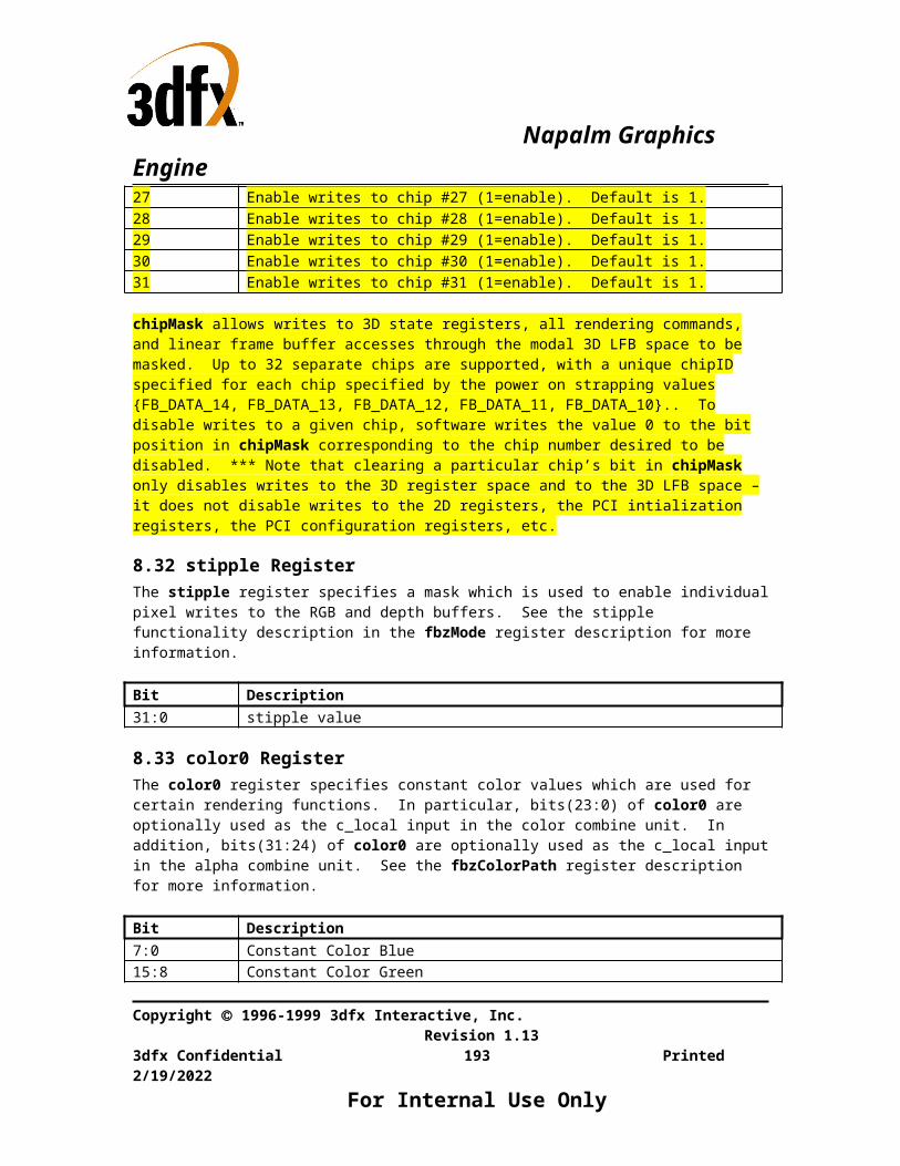
Napalm Graphics Engine Bit Description23:0 24-bits of CMDFIFO address [23:0] in 4k byte pages. Default is 0x0.
15.2 cmdBaseSize0cmdBaseSize0 contains the size of the command fifo in bits 7:0 in 4k byte pages, starting from 4k. Bit 8 enables or disables command fifo 0 operation. Bit 9 defines the location of command fifo 0, a value of 0 locates the command fifo in frame buffer memory, and value of 1 locates the command fifo in AGP memory. Bit 10 disables the hole counter.
Bit Description7:0 Size of CmdFifo in 4k byte pages. (0=4k, 1 = 8k, etc…). Default is 0x0.8 CMDFIFO_0 enable (0=disable, 1=enable). Default is 0x0.9 CMDFIFO_0 resides in AGP (0=frame buffer memory, 1=AGP memory). Default is
0x0.10 Disable hole counter (0=enable, 1=disable). Default is 0x0.
15.3 cmdBump0cmdBump0 defines the number of words to increment the amin pointer by, when managed by software. This register is write only and has no default.
Bit Description15:0 Number of words to bump CMDFIFO 0’s write pointer. Default is 0x0.
15.4 cmdRdPtrL0cmdRdPtrL0 contains the lower 32-bits of the read pointer. This register is read / write and allows software to monitor the progress of the CMDFIFO. This register is read write and has no default value. At initialization, this register should be set to cmdBaseAddr ,expanded to a byte address.
Bit Description31:0 Lower 32-bits of the byte aligned CMDFIFO read pointer. Default is 0x0.
15.5 cmdRdPtrH0cmdRdPtrH0 contains the upper 4-bits of the read pointer. This register is read write and has no default value. At initialization, this register should be set to cmdBaseAddr, expanded to a byte address.
Bit Description3:0 Upper 4-bits of the CMDFIFO read pointer. Default is 0x0.
15.6 cmdAMin0cmdAMin0 is a 25-bit register containing the min address register. CmdAMin register is updated with the cmdAMax register when hole count is zero. This register is read write and has no default value. At initialization this register should be set to cmdBaseAddr - 4. The value read back from this register is 4 more than that written.
Bit Description24:0 Byte Aligned Address Min register, bits 0 and 1 are ignored. Default is 0x0.
Copyright 1996-1999 3dfx Interactive, Inc. Revision 1.133dfx Confidential 193 Printed 5/7/2023
For Internal Use Only

Napalm Graphics Engine 15.7 cmdAMax0cmdAMaxL0 is a 32-bit register containing the 25 bits of the max address register. CmdAMax register is automatically updated when an memory address greater to the existing cmdAMax register is written. At initialization, this register should be set to cmdBaseAddr - 4. The value read back from this register is 4 more than that written.
Bit Description24:0 Byte Aligned Address Max register, bits 0 and 1 are ignored. Default is 0x0.
15.8 cmdStatus0cmdStatus0 is a 32 bit register that allows debuging and visability of the command fifo hardware. This register is read only, and has no impact on software development.
Bit Description31 AGP (packet 6) data xfer in progress30 Unpacker is busy29 Packet 6 decompress busy28 Host data transfers are complete27 JSR (fetch ctrl) active26 Executed depth = 025 Prefetched depth = 024 On chip fifo is empty23:17 Reserved. Default = 016 JSR (unpacker) active15 Jump tag14:12 Jump command.11 Header Valid10:6 Local State (remaining entries in packet)5:3 Etended Packet Command2:0 Packet Type
15.9 cmdFifoDepth0cmdFifoDepth0 is a 20-bit register containing the current depth of CMDFIFO 0. Depth is the number of remaining unexecuted commands in off chip memory. The CMDFIFO is allowed to read upto, but not over the number of entries indicated by cmdFifoDepth register. This register is read write and has no default value.
Bit Description19:0 CMDFIFO 0 depth. Default is 0x0.
15.10 cmdHoleCnt0cmdHoleCnt0 contains the number of unwritten locations between cmdAMin and cmdAMax.
Bit Description15:0 CMDFIFO Hole counter. Default is 0x0.
15.11 cmdBaseAddr1cmdBaseAddrL1 is similar to cmdBaseAddr0, but controls CMDFIFO 1.
Copyright 1996-1999 3dfx Interactive, Inc. Revision 1.133dfx Confidential 194 Printed 5/7/2023
For Internal Use Only
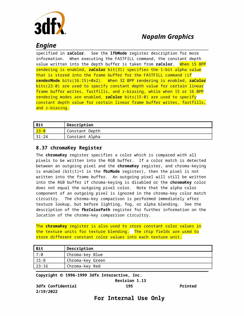
Napalm Graphics Engine Bit Description23:0 Lower 23-bits of CMDFIFO address [31:0] in 4k pages. Default is 0x0.
15.12 cmdBaseSize1cmdBaseSize1 is similar to cmdBaseAddr0, but controls CMDFIFO 1.
Bit Description7:0 Size of CmdFifo in 4k byte pages. Default is 0x0.8 CMDFIFO_1 enable (0=disable, 1=enable). Default is 0x0.9 CMDFIFO_1 resides in AGP (0=frame buffer memory, 1=AGP memory). Default is
0x0.10 Disable hole counter (0=enable, 1=disable). Default is 0x0.
15.13 cmdBump1cmdBump1 is similar to cmdBump0.
Bit Description15:0 Number of words to bump CMDFIFO 1’s write pointer. Default is 0x0.
15.14 cmdRdPtrL1cmdRdPtrL1 is similar to cmdRdPtrL0.
Bit Description31:0 Lower 32-bits of the CMDFIFO read pointer. Default is 0x0.
15.15 cmdRdPtrH1cmdRdPtrH1 is similar to cmdRdPtrH1.
Bit Description3:0 Upper 4-bits of the CMDFIFO read pointer. Default is 0x0.
15.16 cmdAMin1cmdAMin1 is similar to cmdAMin0
Bit Description24:0 Byte Aligned Address Min register for command stream 1. Default is 0x0.
15.17 cmdAMax1cmdAMax1 is similar to cmdAMax0
Bit Description24:0 Byte Aligned Address Max register for command stream 1. Default is 0x0.
15.18 cmdStatus1cmdStatus1 is identical to cmdStatus0, but is used for the second command fifo.
Copyright 1996-1999 3dfx Interactive, Inc. Revision 1.133dfx Confidential 195 Printed 5/7/2023
For Internal Use Only
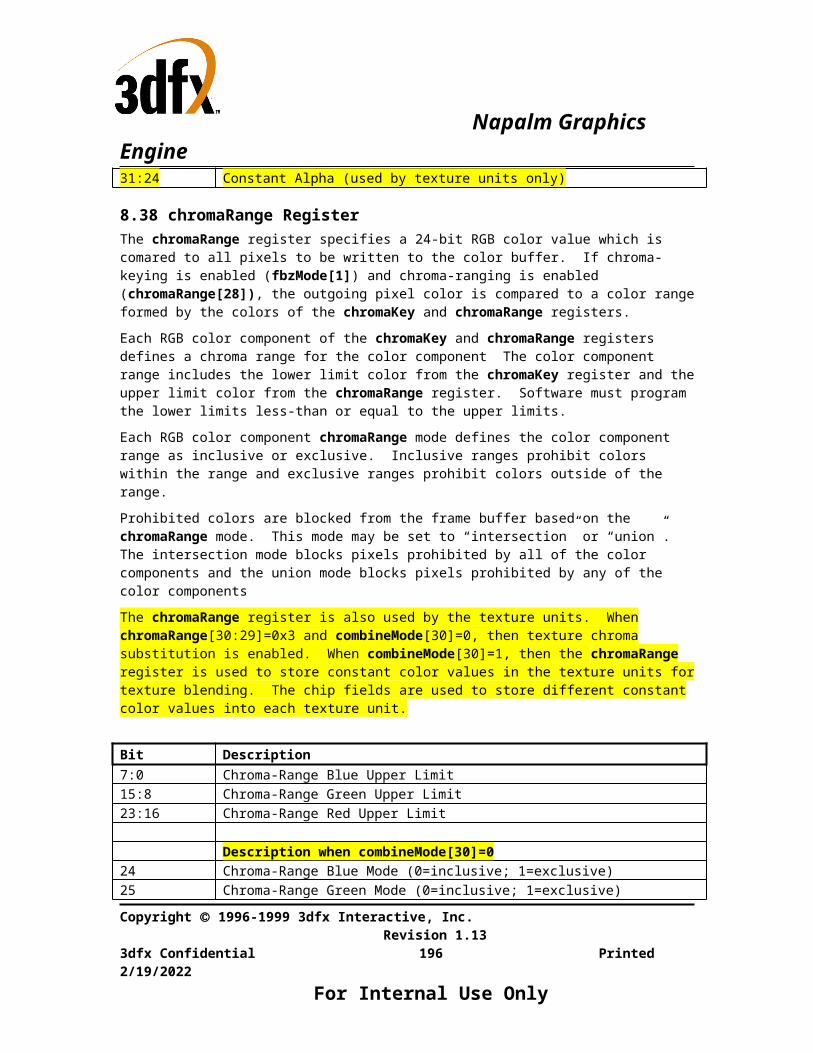
Napalm Graphics Engine 15.19 cmdFifoDepth1cmdFifoDepth1 is similar to cmdFifoDepth0
Bit Description19:0 CMDFIFO 1 depth in dwords. . Default is 0x0.
15.20 cmdHoleCnt1cmdHoleCnt1 is similar to cmdHoleCnt0
Bit Description15:0 CMDFIFO 1’s hole counter. Default is 0x0.
15.21 cmdFifoThresh{cmdFifoThresh[11], cmdFifoThresh[4:0]} contain the fetch threshold, used when the fifo freespace is below fetch threshold, then no new requests are made. Bits 10:5 contain the fifo high water mark, when fifo freespace is above the water mark, then fill requests will be generated. When the high water mark is qualified, then new requests are generated.
Bit Description4:0 CMDFIFO 0 and 1’s fifo fetch threshold (low water mark), lower 5 bits (Default value
is 0).10:5 CMDFIFO 0 and 1’s fifo high water mark (Default value is 7).11 CMDFIFO 0 and 1’s fifo fetch threshold (low water mark), msb bit (Default value is 0).21:12 reserved
15.22 cmdHoleIntcmdHoleInt bits 21:0 contain the number of MCLK cycles a hole counter can have a hole before genreating an interrupt. The counter is only enabled when bit 22 of this register is set. This register should be used in combination with the IntrCtrl register to product PCI interrupts for flagging insufficient data.
Bit Description21:0 CMDFIFO 0 and 1 (holes !=0) time out value. Default is 0x0.22 CMDFIFO Time Out Counter Enable. (0=Disable, 1 = Enable). Default is 0x0.
15.23 yuvBaseAddressyuvBaseAddress register contains the starting frame buffer location of the yuv aperture.
Bit Description25:0 YUV base Address. Default is 0x0.
15.24 yuvStrideyuvStride register contains the destination stride value of the U and V planes.
Bit Description13:0 Y, U and V stride register. Default is 0x0.30:14 reserved31 Destination is tiled (0 = linear, 1 = tiled) . Default is 0x0.
Copyright 1996-1999 3dfx Interactive, Inc. Revision 1.133dfx Confidential 196 Printed 5/7/2023
For Internal Use Only
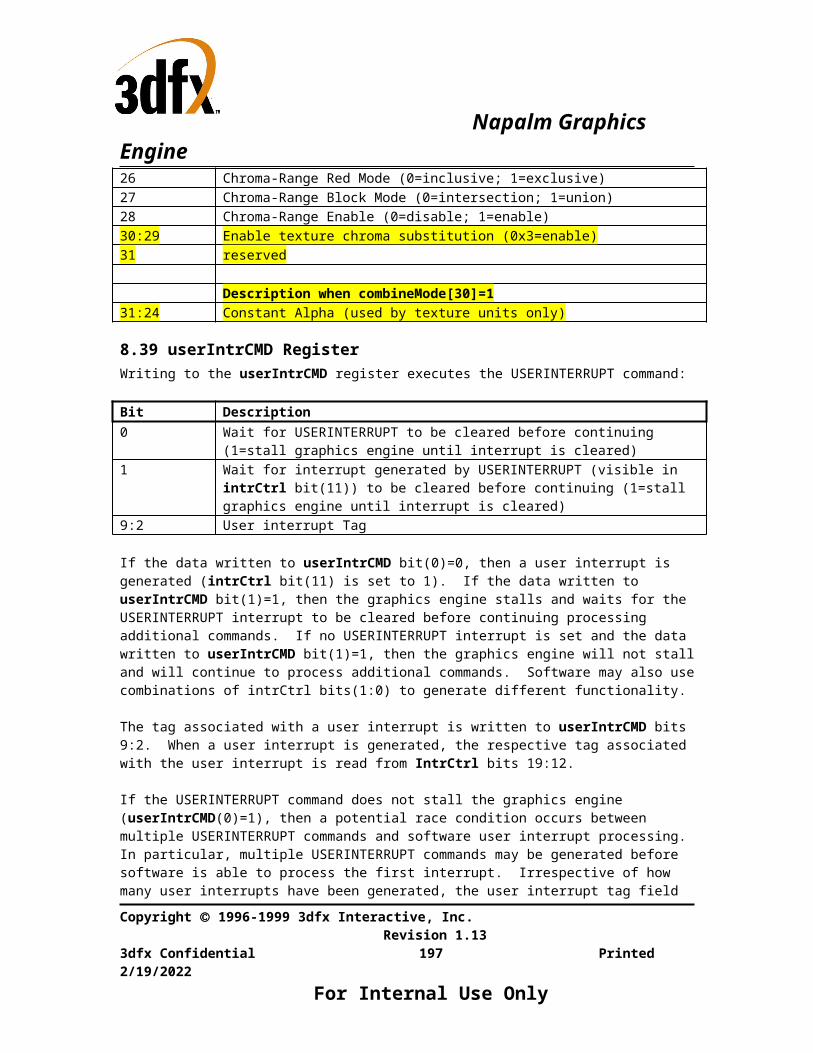
Napalm Graphics Engine
16. AGP/PCI Configuration Register Set
Register Name Addr Bits DescriptionVendor_ID 0 15:0 3dfx Interactive Vendor IdentificationDevice_ID 2 15:0 Device IdentificationCommand 4 15:0 PCI bus configurationStatus 6 15:0 PCI device statusRevision_ID 8 7:0 Revision IdentificationClass_code 9 23:0 Generic functional description of PCI deviceCache_line_size 12 7:0 Bus Master Cache Line SizeLatency_timer 13 7:0 Bus Master Latency TimerHeader_type 14 7:0 PCI Header TypeBIST 15 7:0 Build In Self-Test ConfigurationmemBaseAddr0 16 31:0 Memory Base Address (Init/3D/2D regs)memBaseAddr1 20 31:0 Memory Base Address (LFB)IoBaseAddr 24 31:0 I/O Base AddressReserved 28-43 ReservedSubVendorID 44-45 15:0 Subsystem Vendor IDSubSystemID 46-47 15:0 Subsystem IDRomBaseAddr 48 31:0 Expansion Rom Base AddressCapabilites Ptr 52 31:0 Pointer to start of New Capabilities structure [7:0]Reserved 56-59 ReservedInterrupt_line 60 7:0 Interrupt MappingInterrupt_pin 61 7:0 External Interrupt ConnectionsMin_gnt 62 7:0 Bus Master Minimum Grant TimeMax_lat 63 7:0 Bus Master Maximum Latency TimeFabID 64 7:0 Fab IdentificationcfgInitEnable 65-67 Misc. configuration controlACPI Reset 68-71 31:0 ACPI ResetcfgPciDecode 72-75 31:0 PCI decode logic controlCfgStatus 76 31:0 Aliased memory-mapped status registerCfgScratch 80 31:0 Scratch pad registerAGP Cap_ID 84 31:0 AGP Capability identifier register (read only)AGP status 88 31:0 AGP status register (read only)AGP_Cmd 92 31:0 AGP command register (read / write)ACPI Cap ID 96 31:0 ACPI Capability identifier register (read only)ACPI cntrl/status 100 31:0 ACPI Control and Status register (read / write)Reserved 101-127 ReservedcfgVideoCtrl0 128-131 31:0 Enhanced video control register #0cfgVideoCtrl1 132-135 31:0 Enhanced video control register #1cfgVideoCtrl2 136-139 31:0 Enhanced video control register #2cfgSliLfbCtrl 140-143 31:0 Linear frame buffer access control for SLIcfgAaDepthBufferAperture
144-147 31:0 Tiled aperture specification for SLI/AA lfb accesses
cfgAALfbCtrl 148-151 31:0 Linear frame buffer access control for Anti-Aliasing
agpTestCtrl 152-155 31:0 AGP Test controlCopyright 1996-1999 3dfx Interactive, Inc. Revision 1.133dfx Confidential 197 Printed 5/7/2023
For Internal Use Only
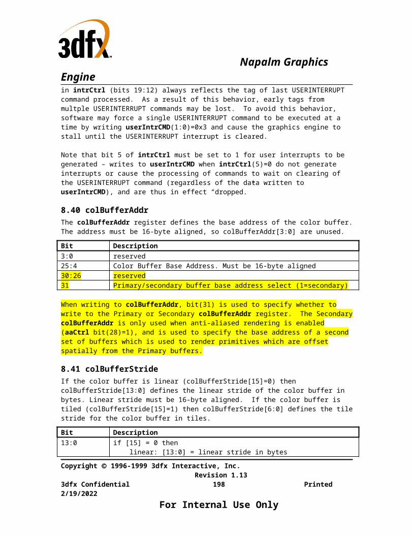
Napalm Graphics Engine agpTestData0 156-159 31:0 AGP Test Data 0agpTestData1 160-163 31:0 AGP Test Data 1agpTestData2 164-167 31:0 AGP Test Data 2agpTestData3 168-171 31:0 AGP Test Data 3cfgSliAaMisc 172-175 31:0 Miscellaneous control for SLI and AAReserved 176-255 n/a Reserved
16.1 Vendor_ID RegisterThe Vendor_ID register is used to identify the manufacturer of the PCI device. This value is assigned by a central authority that will control issuance of the values. This register is read only.
Bit Description7:0 3dfx Interactive Vendor Identification. Default is 0x121a.
16.2 Device_ID RegisterThe Device_ID register is used to identify the particular device for a given manufacturer. This register is read only.
Bit Description15:0 Napalm Device Identification.
Napalm: The values supported are {6,7,8,9}. The lsb of the device ID is controlled by a packaging option, while the selection of either {6,7} or {8,9} is controlled by the power on strapping value of TV_DATA_6. The standard packaging bondout will make the lsb ‘1’.Napalm2: The values supported are {10,11,12,13}. The lsb of the device ID is controlled by a packaging option, while the selection of either {10,11} or {12,13} is controlled by the power on strapping value of TV_DATA_6. The standard packaging bondout will make the lsb ‘1’.
16.3 Command RegisterThe Command register is used to control basic PCI bus accesses. See the PCI specification for more information. Bit 0,1 and 5 are R/W, and bits 15:6 and 4:2 are read only.
Bit Description0 I/O Access Enable. Default is 0.1 Memory Access Enable (0=no response to memory cycles). Default is 0.2 Master Enable. Default is 0.3 Special Cycle Recognition. Default is 0.4 Memory Write and Invalidate Enable. Default is 0.5 Palette Snoop Enable. Default is 0.6 Parity Error Respond Enable. Default is 0.7 Wait Cycle Enable. Default is 0. (strapped)8 System Error Enable. Default is 0.15:9 reserved. Default is 0x0.
16.4 Status RegisterThe Status register is used to monitor the status of PCI bus-related events. This register is read only and is hardwired to the value 0x0.
Copyright 1996-1999 3dfx Interactive, Inc. Revision 1.133dfx Confidential 198 Printed 5/7/2023
For Internal Use Only

Napalm Graphics Engine
Bit Description3:0 Reserved. Default is 0x0.4 New Capabilities (AGP/ACPI). Default is 1 for AGP/ACPI (Strapped)5 66 Mhz Capable. Default is 0 for PCI 33 Mhz 1 for AGP (Strapped)6 UDF supported. Default is 0.7 Fast Back-toBack capable. Default is 0. (Strapped)8 Data Parity Reported. Default is 0. 10:9 Device Select Timing. Default is 0x0.11 Signaled Target Abort. Default is 0.12 Received Target Abort. Default is 0.13 Received Master Abort. Default is 0.14 Signaled System Error. Default is 0.15 Detected Parity Error. Default is 0. Cleared by writing this register. This feature is
used for detecting parity errors on bus transfers.
16.5 Revision_ID RegisterThe Revision_ID register is used to identify the revision number of the PCI device. This register is read only.
Bit Description7:0 Napalm Revision Identification. Default is 0x1 for Rev. A silicon .
16.6 Class_code RegisterThe Class_code register is used to identify the generic functionality of the PCI device. See the PCI specification for more information. This register is read only.
Bit Description23:0 Class Code. Default is 0x3.
16.7 Cache_line_size RegisterThe Cache_line_size register specifies the system cache line size in doubleword increments. It must be implemented by devices capable of bus mastering. This register is read only and is hardwired to 0x0.
Bit Description7:0 Cache Line Size. Default is 0x0.
16.8 Latency_timer RegisterThe Latency_timer register specifies the latency of bus master timeouts. It must be implemented by devices capable of bus mastering. This register is read only and is hardwired to 0x0.
Bit Description7:0 Latency Timer. Default is 0x0.
Copyright 1996-1999 3dfx Interactive, Inc. Revision 1.133dfx Confidential 199 Printed 5/7/2023
For Internal Use Only
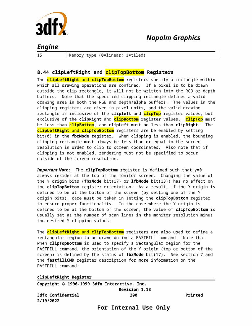
Napalm Graphics Engine 16.9 Header_type RegisterThe Header_type register defines the format of the PCI base address registers (memBaseAddr in Napalm). Bits 0:6 are read only and hardwired to 0x0. Bit 7 of Header_type specifies Napalm as a single function PCI device.
Bit Description6:0 Header Type. Default is 0x0.7 Multiple-Function PCI device (0=single function, 1=multiple function). Default is 0x0.
Bit Description7:0 BIST field and configuration. Default is 0x0.
Poweron strapping {FB_DATA_3, FB_DATA_2, FB_DATA_1, FB_DATA_0}
memBaseAddr0 default value
0 (4’b0000) 0xf800_0000 (128 MBytes allocated)1 (4’b0001) 0xf000_0000 (256 MBytes allocated)2 (4’b0010) 0xe000_0000 (512 MBytes allocated)3 (4’b0011) 0xc000_0000 (1024 MBytes allocated)4 (4’b0100) 0xfc00_0000 (64 MBytes allocated)5 (4’b0101) 0xfe00_0000 (32 MBytes allocated)6 (4’b0110) 0xff00_0000 (16 MBytes allocated)7 (4’b0111) 0xff80_0000 (8 MBytes allocated)8 (4’b1000) 0xffc0_0000 (4 MBytes allocated)9-15 reserved
Copyright 1996-1999 3dfx Interactive, Inc. Revision 1.133dfx Confidential 200 Printed 5/7/2023
For Internal Use Only
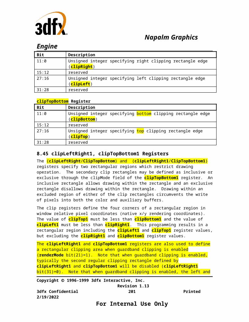
Napalm Graphics Engine The value of memBaseAddr0[3] is always zero, indicating a non-prefetchable address space.
Once POST has occurred and system memory has been allocated for memBaseAddr0, software may change the amount of memory space decoded for the memBaseAddr0 address space using pciCfgDecode[3:0] as follows:
pciCfgDecode[3:0] Amount of address space decoded in memBaseAddr0 address space
0 128 MBytes1 256 MBytes2 512 MBytes3 1024 MBytes4 64 MBytes5 32 MBytes6 16 MBytes7 8 MBytes8 4 MBytes9-15 reserved
Typically for multi-board configurations, the amount of memory allocated for the chip setup to be PCI function number zero will allocate more memory than actually required, then once POST has occurred the software drive will configure the remaining non-mapped chips within the memory allocated by the PCI function zero chip. Upper bits of the memBaseAddr0 register can be modified by software once cfgInitEnable[10] is set.
Bit Description31:0 Memory Base #0 Address
16.12 memBaseAddr1 RegisterThe memBaseAddr1 register determines a second base address for PCI memory mapped accesses to Napalm. Writing 0xffffffff to this register will reset it to its default state. Once memBaseAddr1 has been reset, it can be probed by software to determine the amount of memory space required for Napalm. A subsequent write to memBaseAddr1 will set the memory base address for all PCI memory accesses. See the PCI specification for more details on memory base address programming.
CPU reads and writes to the memBaseAddr1 address space are used to directly access the frame buffer memory.
The default value of memBaseAddr1 is determined by the poweron reset value of {FB_DATA_7, FB_DATA_6, FB_DATA_5, FB_DATA_4} as follows:
Poweron strapping {FB_DATA_7, FB_DATA_6, FB_DATA_5, FB_DATA_4}
memBaseAddr1 default value
0 (4’b0000) 0xf800_0008 (128 MBytes allocated)1 (4’b0001) 0xf000_0008 (256 MBytes allocated)2 (4’b0010) 0xe000_0008 (512 MBytes allocated)3 (4’b0011) 0xc000_0008 (1024 MBytes allocated)
Copyright 1996-1999 3dfx Interactive, Inc. Revision 1.133dfx Confidential 201 Printed 5/7/2023
For Internal Use Only
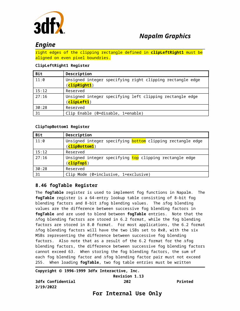
Napalm Graphics Engine
4 (4’b0100) 0xfc00_0008 (64 MBytes allocated)5 (4’b0101) 0xfe00_0008 (32 MBytes allocated)6 (4’b0110) 0xff00_0008 (16 MBytes allocated)7 (4’b0111) 0xff80_0008 (8 MBytes allocated)8 (4’b1000) 0xffc0_0008 (4 MBytes allocated)9-15 reserved
The value of memBaseAddr1[3] is always one, indicating a prefetchable address space.
Once POST has occurred and system memory has been allocated for memBaseAddr1, software may change the amount of memory space decoded for the memBaseAddr1 address space using pciCfgDecode[7:4] as follows:
pciCfgDecode[7:4] Amount of address space decoded in memBaseAddr1 address space
0 128 MBytes1 256 MBytes2 512 MBytes3 1024 MBytes4 64 MBytes5 32 MBytes6 16 MBytes7 8 MBytes8 4 MBytes9-15 reserved
Typically for multi-board configurations, the amount of memory allocated for the chip setup to be PCI function number zero will allocate more memory than actually required, then once POST has occurred the software drive will configure the remaining non-mapped chips within the memory allocated by the PCI function zero chip. Upper bits of the memBaseAddr1 register can be modified by software once cfgInitEnable[10] is set.
Bit Description31:0 Memory Base #1 Address
16.13 ioBaseAddr RegisterThe memBaseAddr register determines the base address for all PCI IO mapped accesses to Napalm. Writing 0xffffffff to this register will reset it to its default state. Once ioBaseAddr has been reset, it can be probed by software to determine the amount of io space required for Napalm. A subsequent write to ioBaseAddr will set the IO base address for all PCI memory accesses. See the PCI specification for more details on IO base address programming.
The default value of ioBaseAddr is determined by the poweron reset value of {FB_DATA_9, FB_DATA_8} as follows:
Poweron strapping {FB_DATA_9, FB_DATA_8}
ioBase default value
0 (2’b00) 0xffff_ff01 (256 bytes allocated)1 (2’b01) 0xffff_fe01 (512 bytes allocated)
Copyright 1996-1999 3dfx Interactive, Inc. Revision 1.133dfx Confidential 202 Printed 5/7/2023
For Internal Use Only

Napalm Graphics Engine
2 (2’b10) 0xffff_fc01 (1024 bytes allocated)3 (2’b11) 0xffff_f801 (2048 bytes allocated)
Once POST has occurred and system memory has been allocated for ioBaseAddr, software may change the amount of IO space decoded using pciCfgDecode[9:8] as follows:
pciCfgDecode[9:8] Amount of address space decoded in ioBaseAddr address space
0 256 bytes1 512 bytes2 1024 bytes3 2048 bytes
Bit Description31:0 IO Base Address
16.14 subVendorID RegisterThe subVendorID register defines the board manufacturer ID. During system initialization the expansion code located at romBaseAddr will set this register to the appropriate value. This register is read during plug and play initialization. See the PC97 specification for more details on subVendorID and plug and play requirements. The default value for this register is automaticaly loaded after reset from the ROM. Bits 7:0 are stored in ROM location 0x7ff8, while bits 15:8 are stored in 0x7ff9 for a 32K ROM. Bits 7:0 are stored in ROM location 0xfff8, while bits 15:8 are stored in 0xfff9 for a 64K ROM.Bit Description15:0 Subsystem Vendor ID register. Initialized by expansion prom, default is read by ROM.
16.15 subSystemID RegisterThe subSystemID register defines the board type. During system initialization, the expansion code located at romBaseAddr will set this register to the appropriate value. This register is read during plug and play initialization. See the PC97 specification for more details on subSystemID and plug and play requirements. The default value for this register is automaticaly loaded after reset from the ROM. Bits 7:0 are stored in ROM location 0x7ffa, while bits 15:8 are stored in 0x7ffb for a 32K ROM. Bits 7:0 are stored in ROM location 0xfffa, while bits 15:8 are stored in 0xfffb for a 64K ROM.
Bit Description15:0 Subsystem ID register. Initialized by expansion prom, default is read by ROM.
16.16 romBaseAddr RegisterThe romBaseAddr register determines the base address for all PCI ROM accesses to Napalm. Writing 0xfffffffe to this register will reset it to its default state. Once romBaseAddr has been reset, it can be probed by software to determine the amount of ROM space required for Napalm. A subsequent write to romBaseAddr will set the ROM base address for all PCI memory accesses. See the PCI specification for more details on memory base address programming. Napalm requires 32 to 64 Kbytes of address space for ROM accesses and is configured by strapping bit 2. For ROM accesses on the 32-bit PCI bus, the contents of romBaseAddr are compared with the pci_ad bits 31..16 (upper 16 bits) to determine if Napalm is being accessed. This register is R/W.
Bit DescriptionCopyright 1996-1999 3dfx Interactive, Inc. Revision 1.133dfx Confidential 203 Printed 5/7/2023
For Internal Use Only
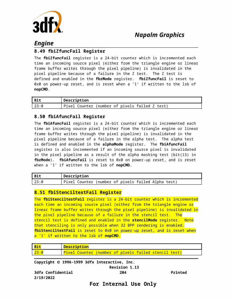
Napalm Graphics Engine 31:0 Expansion Rom Base Address. Default is 0xffff8000 or 0xffff0000.
16.17 Capabilities PointerThe Capabilities pointer register contains the offset in configuration space of beginning of the capability link list structure. This register is read only.
Bit Description31:0 Capabilities Pointer offset. Default is 0x00000054 if AGP is enabled via the strapping
bits, otherwise it is 0x60.
16.18 Interrupt_line RegisterThe Interrupt_line register is used to map PCI interrupts to system interrupts. In a PC environment, for example, the values of 0 to 15 in this register correspond to IRQ0-IRQ15 on the system board. The value 0xff indicates no connection. This register is R/W.
Bit Description0:7 Interrupt Line. Default is 0x5 (IRQ5)
16.19 Interrupt_pin RegisterThe Interrupt_pin register defines which of the four PCI interrupt request lines, INTA* - INTRD*, the PCI device is connected to. This register is read only and is hardwired to 0x1.
Bit Description0:7 Interrupt Pin. Default is 0x1 (INTA*)
16.20 Min_gnt RegisterThe Min_gnt register specifies the burst period a PCI bus master requires. It must be implemented by devices capable of bus mastering. This register is read only and is hardwired to 0x0 since Napalm does not support bus mastering.
Bit Description7:0 Minimum Grant. Default is 0x0.
16.21 Max_lat RegisterThe Max_lat register specifies the maximum request frequency a PCI bus master requires. It must be implemented by devices capable of bus mastering. This register is read only and is hardwired to 0x0 since Napalm does not support bus mastering.
Bit Description7:0 Maximum Latency. Default is 0x0.
16.22 fabID RegisterIdentification code of the manufacturing plant.
Bit Description3:0 Manufacturing fab identification. Read Only. Default is 0x1 (1 = TSMC)
Copyright 1996-1999 3dfx Interactive, Inc. Revision 1.133dfx Confidential 204 Printed 5/7/2023
For Internal Use Only

Napalm Graphics Engine 7:4 Reserved
16.23 ACPI Reset RegisterThe ACPI Reset register returns the status of the internal acpi_reset signal.
Bit Description0 Value of internal acpi_reset signal (read only)31:1 Reserved (read only. Returns 0x0)
16.24 cfgInitEnable RegisterThe cfgInitEnable register is used to control miscellaneous configuration functions.
Bit Description8 Enable writes to hardware initialization registers. (1=enable writes to the hardware
initialization registers). Default is 1.9 Enable writes to PCI FIFO (1=enable writes to PCI FIFO). Default is 1.10 Enable writes to memBaseAddr0 bits(29:22), memBaseAddr1 bits(29:27), and
ioBaseAddr bits(10:8). Default is 0x0. 11 Address snoop enable (1=enable). Default is 0.12 Address snoop memBaseAddr0 enable (1=enable). Default is 0.13 Address snoop memBaseAddr1 enable (1=enable). Default is 0.14 Address snoop Master/Slave (1=slave). Default is 0.24:15 Snoop Address #0. When Address snooping of memBaseAddr0 is enabled
(cfgInitEnable[11]=1 and cfgInitEnable[12]=1), the incoming PCI address high order bits are compared with cfgInitEnable bits(24:15). The amount of address space snooped is controlled by cfgPciDecode[13:10]. The PCI cycle is snooped if the address comparison passes and a memory read transaction is being performed. Note that memory writes are not snooped for memBaseAddr0. Default is 0x0.
25 Swapbuffer algorithm (0=use vsync, 1=use sli_syncin/sli_syncout)26 Swap Master (1=master – only used when cfgInitEnable[25]=1)27 Use “Quick” sampling algorithm on sli_syncin (1=enable – only used when
cfgInitEnable[25]=1).28 PCI multi-function device (sets bit(7) of the Header_type configuration register).
Default is poweron strap value of FB_DATA_19.29 Disable linear frame buffer read cache (in pci_lfb_rd.v) (1=disable)30 Enable snooped writes to hardware initialization registers (1=enable)31 reserved
16.25 cfgPciDecode RegisterThe cfgPciDecode register is used to control the amount of memory decoded for the various memory bases in Napalm.
Bit Description3:0 pci_membase0_decode. Default is poweron strap value of {FB_DATA_3,
FB_DATA_2, FB_DATA_1, FB_DATA_0}7:4 pci_membase1_decode. Default is poweron strap value of {FB_DATA_7,
FB_DATA_6, FB_DATA_5, FB_DATA_4}9:8 pci_iobase_decode. Default is poweron strap value of {FB_DATA_9, FB_DATA_8}13:10 snoop_membase0_decode. Default is 0x0.
Copyright 1996-1999 3dfx Interactive, Inc. Revision 1.133dfx Confidential 205 Printed 5/7/2023
For Internal Use Only
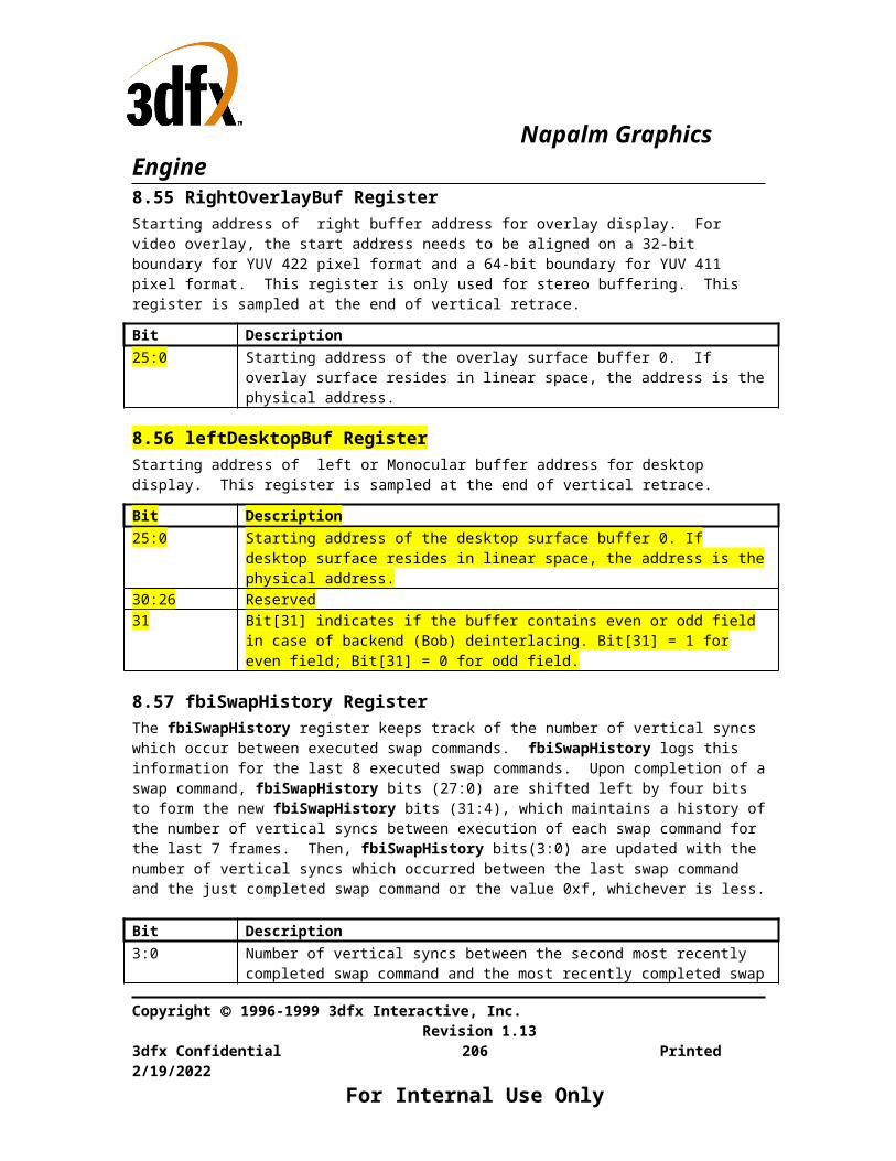
Napalm Graphics Engine 17:14 snoop_membase1_decode. Default is 0x0.27:18 Snoop Address #1. When Address snooping of memBaseAddr1 is enabled
(cfgInitEnable[11]=1 and cfgInitEnable[13]=1), the incoming PCI address high order bits are compared with cfgPciDecode bits(27:18). The amount of address space snooped is controlled by cfgPciDecode[17:14]. The PCI cycle is snooped if the address comparison passes and a memory read or write transaction is being performed. Default is 0x0.
31:28 reserved
The amount of memory decoded for memBaseAddr0 and memBaseAddr1 (as controlled by cfgPciDecode[3:0] and cfgPciDecode[7:4] respectively), and the amount of memory snooped for memBaseAddr0 and memBaseAddr1 (as controlled by cfgPciDecode[13:10] and cfgPciDecode[17:14] is as follows:
pciCfgDecode[xx:yy] Amount of address space decoded in particular address space
0 128 MBytes1 256 MBytes2 512 MBytes3 1024 MBytes4 64 MBytes5 32 MBytes6 16 MBytes7 8 MBytes8 4 MBytes9-15 reserved
The amount of IO space decoded for ioBaseAddr (as controlled by cfgPciDecode[9:8]) is as follows:
pciCfgDecode[xx:yy] Amount of address space decoded in particular address space
0 256 bytes1 512 bytes2 1024 bytes3 2048 bytes
16.26 cfgVideoCtrl0, cfgVideoCtrl1, and cfgVideoCtrl2 RegistersThe cfgVideoCtrl0, cfgVideoCtrl1, and cfgVideoCtrl2 registers control the scanline interleave and anti-aliasing capabilities of the video unit of Napalm.
cfgVideoCtrl0 register (Default is 0x0).Bit Description0 enhanced_video_en (1=enable)1 enhanced_video_slv (1=enhanced video slave)2 video_tv_output_en (1=unconditionally drive tv control and data signals)3 video_localmux_sel (1=select sum of overlay and desktop)5:4 video_othermux_sel_true[1:0]7:6 video_othermux_sel_false[1:0]
Copyright 1996-1999 3dfx Interactive, Inc. Revision 1.133dfx Confidential 206 Printed 5/7/2023
For Internal Use Only

Napalm Graphics Engine 8 sli_fetch_compare_invert (1=invert)9 sli_crt_compare_invert (1=invert)10 sli_aafifo_compare_invert (1=invert)11 vidpll_sel (0=normal operation, 1=sync slave chip to Master’s clock)14:12 divide_video (0=no divide, 1=divide by 2, 2=divide by 4, 3=divide by 8, 4=divide by
16, 5=divide by 32, 6-7=undefined)15 always_drive_aa_bus (1=always drive AA data bus when cfgVideoCtrl0[1:0]=0x3)19:16 Delay value for vsync_ref signal23:20 reserved24 dac_vsync_tristate (1=unconditionally tristate dac_vsync signal)25 dac_hsync_tristate (1=unconditionally tristate dac_hsync signal)31:26 reserved
cfgVideoCtrl1 register (Default is 0x0).Bit Description7:0 sli_rendermask_fetch15:8 sli_comparemask_fetch23:16 sli_rendermask_crt31:24 sli_comparemask_crt
cfgVideoCtrl2 register (Default is 0x0).Bit Description7:0 sli_rendermask_aafifo15:8 sli_comparemask_aafifo31:16 reserved
The cfgVideoCtrl0, cfgVideoCtrl1, cfgVideoCtrl2, and cfgVideoCtrl3 registers control the following external signals:
Signal Name Descriptiondac_vsync The dac_vsync signal is always tristated when dac_vsync_float is set, regardless
of all other settings. When dac_vsync_float is cleared and enhanced_video_en is set, then dac_vsync is driven if enhanced_video_slv is cleared (and tristated if enhanced_video_slv is set).
dac_hsync The dac_hsync signal is always tristated when dac_hsync_float is set, regardless of all other settings. When dac_hsync_float is cleared and enhanced_video_en is set, then the following equation is used to determine whether dac_hsync is driven:
(((scanline[7:0] & sli_rendermask_crt) == sli_comparemask_crt) ^ sli_crt_compare_invert)
If enhanced_video_en is set and the above equation is true, then dac_hsync is driven, otherwise dac_hsync is tristated.
TV control signals (tv_clk_out, tv_hsync, tv_vsync, tv_blank)
If video_tv_output_en is set, then the TV control signals are driven, regardless of all other settings. If video_tv_output_en is cleared and enhanced_video_en is set, then the TV control signals are driven if enhanced_video_slv is cleared, otherwise if enhanced_video_en and enhanced_video_slv are both set then the TV control signals are tristated.
tv_data[11:0] If video_tv_output_en is set, then the tv_data signals are driven, regardless of all other settings. If video_tv_output_en is cleared and enhanced_video_en is set,
Copyright 1996-1999 3dfx Interactive, Inc. Revision 1.133dfx Confidential 207 Printed 5/7/2023
For Internal Use Only
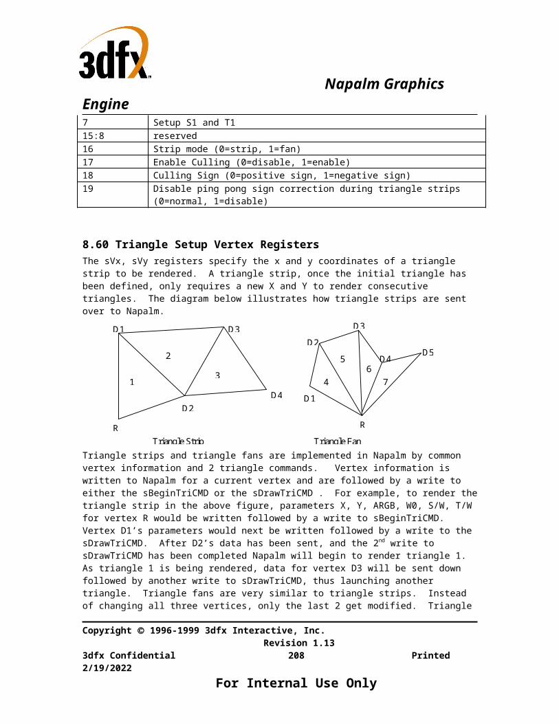
Napalm Graphics Engine
then the following equation is used to determine whether the tv_data signals are driven:
(((scanline[7:0] & sli_rendermask_crt) == sli_comparemask_crt) ^ sli_crt_compare_invert)
If enhanced_video_en is set and the above equation is true, then the tv_data signals are driven, otherwise the tv_data signals are tristated.
Digital AA signals (aa_vld, aa_clk, aa_data[11:0], vmi_addr[3:0], vmi_data[7:0], vmi_rw, vmi_ds_n, vmi_rdy)
If enhanced_video_en is set and enhanced_video_slv is set, then the following equation is used to determine whether the digital AA signals are driven:
(((scanline[7:0] & sli_rendermask_aafifo) == sli_comparemask_aafifo) ^ sli_aafifo_compare_invert)
If enhanced_video_en is set and enhanced_video_slv is set and the above equation is true, then the digital AA signals are driven, otherwise if enhanced_video_en is set and enhanced_video_slv is cleared the Digital AA signals are tristated. (Note that if enhanced_video_en is set then the VMI host bus signals are controlled by the above rules, otherwise if enhanced_video_en is cleared then the VMI host bus signals are controlled by the VMI control logic). *** Note that valid data is only transferred on the digital AA signals when enhanced_video_en is set and the above equation is true – otherwise aa_vld is tristated and no valid data is transferred across the digital AA bus.
The cfgVideoCtrl0, cfgVideoCtrl1, and cfgVideoCtrl2 registers also control the following internal signals:
Signal Description Descriptionvideo_fifo_push When enhanced_video_en is set, then the following equation is used to
determine whether video data is requested from the frame buffer and pushed onto the video fifo:
(((scanline[7:0] & sli_rendermask_fetch) == sli_comparemask_fetch) ^ sli_fetch_compare_invert)
If enhanced_video_en is set and the above equation is true, then video data is requested from the frame buffer and pushed onto the video fifo, otherwise no video data is requested and no data is pushed onto the video fifo.
video_fifo_pop When enhanced_video_en is set, then the following equation is used to determine whether video data is popped off the video fifo:
(((scanline[7:0] & sli_rendermask_fetch) == sli_comparemask_fetch) ^ sli_fetch_compare_invert)
If enhanced_video_en is set and the above equation is true, then video data is popped off the video fifo during display refresh. *** Note that if enhanced_video_en is set and the above equation is not true that no data is popped off the video fifo (implying that the data to be presented to the monitor will be received from the AA fifo).
aafifo_pop When enhanced_video_en is set, then the following equation is used to control the aafifo_pop signal:
(((scanline[7:0] & sli_rendermask_aafifo) == sli_comparemask_aafifo) ^ sli_aafifo_compare_invert)
If enhanced_video_en is set and the above equation is true, then aafifo_pop is asserted, otherwise aafifo_pop is deasserted. *** Note that if the AA fifo is empty, that aafifo_pop is deasserted regardless of the result of the equation above (i.e. a pop will never be generated which would underflow the fifo).
Copyright 1996-1999 3dfx Interactive, Inc. Revision 1.133dfx Confidential 208 Printed 5/7/2023
For Internal Use Only
Napalm Graphics Engine DAC_blank The DAC_blank signal is asserted during the active video region for a
particular scanline when enhanced_video_en is set and the following equation is false:
(((scanline[7:0] & sli_rendermask_crt) == sli_comparemask_crt) ^ sli_crt_compare_invert)
If enhanced_video_en is set and the above equation is true, then the DAC_blank signal is deasserted during the active video region of a particular scanline.
localmux (MUX #1) select When video_localmux_sel is set, then the output of the video localmux (MUX #1) will be the sum of the desktop and overlay surfaces. If video_localmux_sel is cleared, then the output of the video localmux will be the result of the standard chroma-key comparison. Note that enhanced_video_en has no effect on the output of the video localmux (MUX #1).
othermux (MUX #2) select [1:0] (video_othermux_sel[1:0])
When enhanced_video_en is set, then the following equation is used to control the video othermux (MUX #2) select signals (2 bits):
(((scanline[7:0] & sli_rendermask_aafifo) == sli_comparemask_aafifo) ^ sli_aafifo_compare_invert)
If enhanced_video_en is set and the above equation is true, then the video othermux select signal is video_othermux_sel_true[1:0]. If enhanced_video_en is set and the above equation is false, then the video localmux select signal is video_othermux_sel_false[1:0]. If enhanced_video_en is cleared, then the output of the video othermux (MUX #2) is set to be the output of the video localmux (MUX #1).
16.27 cfgSliLfbCtrl RegisterThe cfgSliLfbCtrl register is used to control the functionality of linear frame buffer accesses when scanline interleaving is enabled.
Bit Description7:0 sli_lfb_renderMask (unsigned value)15:8 sli_lfb_compareMask (unsigned value)23:16 sli_lfb_scanMask (unsigned value)25:24 sli_lfb_numchips_log2 [# chips in SLI (log2)]26 sli_lfb_cpu_wr_en (1=enable) [drop scanlines in memBaseAddr1 SLI/AA tiled space
not owned for direct cpu lfb writes]27 sli_lfb_dptch_wr_en (1=enable) [drop scanlines in memBaseAddr1 SLI/AA tiled space
not owned for dispatched lfb writes – dispatched lfb writes are those which are generated from within a command fifo packet]
28 sli_lfb_rd_en (1=enable) [for a given chip, return only scanlines owned for lfb reads accessing the SLI/AA tiled memory region in memBaseAddr1]
31:28 reserved
16.28 cfgAaDepthBufferAperture RegisterThe cfgAaDepthBufferAperture register is used to define the aperture within the memBaseAddr1 address space which defines the depth buffer location. cfgAaDepthBufferAperture is used by the linear frame buffer read module for AA reads so as to ensure that reads from the depth buffer do not get averaged together to form an anti-aliased result. Instead, reads from the depth buffer do not get averaged and only the values from the primary surface are returned (i.e. only one sub-sample is returned).
Copyright 1996-1999 3dfx Interactive, Inc. Revision 1.133dfx Confidential 209 Printed 5/7/2023
For Internal Use Only
Napalm Graphics Engine Bit Description14:0 aa_depth_buffer_begin (bits[26:12], specified in 4K pages)15 reserved31:16 aa_depth_buffer_end (bits[27:12], specified in 4K pages)
When in a multi-chip configuration using scanline interleaving, sli_lfb_cpu_wr_en is set to cause direct cpu writes in the SLI/AA tiled aperture of memBaseAddr1 to be dropped if a particular scanline is not owned by a given chip. An incoming 27-bit address is within the SLI/AA tiled aperture of memBaseAddr1 if the address is greater than or equal to the tiled aperature beginning (controlled by the lfbMemoryTileCtrl and lfbMemoryTileCompare registers). Similarly, sli_lfb_dptch_wr_en is set to cause dispatched writes (writes within the memBaseAddr1 address space generated by command fifo packets) to be dropped if a particular scanline is not owned by a given chip.
sli_lfb_rd_en is set to cause a given chip to return data from a linear frame buffer read within the SLI/AA tiled aperture of memBaseAddr1. This bit must be set for normal SLI operation.
For both reads and writes to the SLI/AA tiled aperture of memBaseAddr1, the calculated Y value is modified prior to physical address calculation in order to pack scanline “bands” into a particular chips’ memory as follows (exactly the same formula used for rendered as defined in the 3D register sliCtrl):
N = log2(# scanlines rendered by each chip, valid values {1,2,4,8,16,32,64,128}) [0 <= N < 8]M = log2(# chips in SLI configuration, valid values {2,4,8}) [0 < M < 4]ChipID = unique value identifying each chip in an SLI configuration (range 0-7 inclusive)sli_lfb_renderMask = [(# chips in SLI configuration) – 1] << Nsli_lfb_compareMask = chipID << Nsli_lfb_scanMask = 2N – 1sli_lfb_numchips_log2 = M
Note that a combination of M and N must be selected such that sli_lfb_renderMask, sli_lfb_compareMask, and sli_lfb_scanMask are 8-bit quantities (i.e. less than 256).
When either sli_lfb_cpu_wr_en or sli_lfb_dptch_wr_en are set, a linear frame buffer access within the SLI/AA tiled aperture of memBaseAddr1 is written when (y & sli_lfb_renderMask) == sli_lfb_compareMask. The Y value used for physical address calculation is modified when either sli_lfb_cpu_wr_en or sli_lfb_dptch_wr_en are set as follows to reduce the amount of frame buffer memory required for a given chip:
y’ = [(y >> M) & ~ sli_lfb_scanMask] + [y & sli_lfb_scanMask]
16.29 cfgAaLfbCtrl RegisterThe cfgAaLfbCtrl register is used to control the functionality of linear frame buffer accesses when anti-aliasing interleaving is enabled.
Bit Description3:0 reserved25:4 Bits 25:4 of base address for second set of rendering buffers used for anti-aliasing26 aa_lfb_cpu_wr_en (1=enable) [broadcast direct cpu lfb writes within the SLI/AA tiled
aperture of memBaseAddr1 to both AA rendering surfaces]27 aa_lfb_dptch_wr_en (1=enable) [broadcast dispatched lfb writes within the SLI/AA
tiled aperture of memBaseAddr1 to both AA rendering surfaces -- dispatched lfb writes are those which are generated from within a command fifo packet]
28 aa_lfb_rd_en (1=enable) [Enable anti-aliased lfb reads accessing the SLI/AA tiled
Copyright 1996-1999 3dfx Interactive, Inc. Revision 1.133dfx Confidential 210 Printed 5/7/2023
For Internal Use Only

Napalm Graphics Engine
memory aperture of memBaseAddr1]30:29 aa_lfb_rd_format (0=16bpp, 1=15bpp, 2=32bpp, 3=reserved)31 aa_lfb_rd_divide_by_four (0=divide by 2, 1=divide by 4)
aa_lfb_cpu_wr_en is set to cause direct cpu writes in the SLI/AA tiled aperture of memBaseAddr1 to be broadcast to both AA sets of rendering buffers (where the location of the second set of rendering buffers is defined in the Secondary colBufferAddr and Second auxBufferAddr registers). An incoming 27-bit address is within the SLI/AA tiled aperture of memBaseAddr1 if the address is greater than or equal to the tiled aperature beginning (controlled by the lfbMemoryTileCtrl and lfbMemoryTileCompare registers). Similarly, aa_lfb_dptch_wr_en is set to cause dispatched writes (writes within the memBaseAddr1 address space generated by command fifo packets) to be broadcast to both AA sets of rendering buffers.
aa_lfb_rd_en is set to cause all 4 subsample buffers which compose a particular pixel’s value to be averaged together for CPU reads in the SLI/AA tiled aperture of memBaseAddr1. This bit should be set for normal AA operation.
16.30 cfgSliAaMisc RegisterThe cfgSliAaMisc register is used to control miscellaneous configuration functions.
Bit Description8:0 vga_vga_vsync_offset. Default is 0x0.10:9 hotplug signal control (0,1=tristate, 2=drive low, 3=drive high). Default is 0x0. The
hotplug signal needs to be an input when used for LCD hotplug functionality, and thus cfgSliAaMisc bits(10:9) should be 0x0 when this functionality is desired.
11 hotplug pin value (input value of the hotplug pin). Default is 0.12 aa_lfb_rd_slv_wait (1=wait for aa data to be transferred before transfering own data).
Default is 0. Used for greater than 2-chip multi-chip configurations31:13 reserved
The vga_vga_vsync_offset field (cfgSliAaMisc[8:0]) is programmed as follows (copied from Rich Goodin’s email):
The following is the description of how to program the three fields of vga_vsync_offset:
vga_vsync_offset is a 9 bit field subdivided into three 3 bit subfields. vga_vsync_offset[2:0] is pixel offset and shifts the synchronization point in pixel increments. vga_vsync_offset[5:3] is character offset and shifts the synchronization point in character (8 pixel) increments. vga_vsync_offset[8:6] is a bit more difficult to explain as it is a preset for the internalhoriz_xtra signal. The present value can range for 0-5 and I'll explain how it is determined below.
The VGA horizontal timing is based on the value of a horizontal counter. The width of the scan line is specified by setting the maximum horizontal count by writing the horizontal total register. But, as with all things VGA, the scanline length is not simply horizontal total character times, but horizontal total + 5 character times. Internally, the VGA counts to horizontal total and then counts horizontal xtra for 5 more character times.
The vsync_ref signal is passed through a "debounce" network which introduces a delay of approximately 16 character clock cycles. The goal of loading the vga_vsync_offset values is to preset the slave VGA CRTC to the correct state the delay time after the master's vsync start. In
Copyright 1996-1999 3dfx Interactive, Inc. Revision 1.133dfx Confidential 211 Printed 5/7/2023
For Internal Use Only
Napalm Graphics Engine
the case of the delay being exactly 16 pixel clocks the following settings would sync up the master andslave exactly. If the desire is to actually cause the slave to run ahead of the master then increase the values, if the desire is to run after, decrease the values.
For the 16 bit delay, this breaks down to 2 characters and not pixels or vga_vsync_offset[2:0] is set to 0 and vga_vsync_offset[5:3] is set to 2. vga_vsync_offset[8:6] is set depending on the setting of hsync_start. If the programmed delay value is set up to occur prior to horizontal total, thevalue is set to 0. If the delay value is past horizontal total then the programmed value is set as follows:
If hsync_start + character delay <= horizontal total, vga_vsync_offset[8:6] = 0.If hsync_start + character delay == horizontal total+1, vga_vsync_offset[8:6] =1. And so on to the maximum value of 5.
*** Note that Napalm has a bug which makes the value vga_vsync_offset[2:0]=7 behave as if vga_vsync_offset[2:0]=15, so vga_vsync_offset[5:3] must be adjusted accordingly.
16.31 cfgStatus RegisterThe cfgStatus register is an alias to the normal memory-mapped status register. See section x.x for a description of the status registers. Reading the configuration space cfgStatus register returns the same data as if reading from the memory-mapped status register.
16.32 cfgScratch RegisterThe cfgScratch register can be used as scratch pad storage space by software. The values of cfgScratch are not used internally to alter functionality, so any value can be stored to and read from cfgScratch.
Bit Description31:0 Scratchpad register. Default is 0x0.
16.33 New capabilities (AGP and ACPI)AGP and ACPI Use PCI’s new capabilities mechanism. The New Capabilities structure is implemented as a linked list of registers containing information for each function supported by Napalm. The list contains both AGP status and command registers. AGP registers read back ‘0’ if AGP is disabled via the strapping pins.
16.34 Capability Identifier RegisterThe capability register resides at offset (CAP_OFFSET). This register identifies AGP revision compliance
Bit Description7:0 Capability ID. Always == 2 for AGP15:8 Next Capability ID Pointer. Default is 0x60.19:16 Minor AGP revision, the interface conforms to23:20 Major AGP revision, the interface conforms to
Copyright 1996-1999 3dfx Interactive, Inc. Revision 1.133dfx Confidential 212 Printed 5/7/2023
For Internal Use Only
Napalm Graphics Engine 31:24 Reserved. Defined as 0.
16.35 AGP StatusAGP status register documents maximum number of requests that Napalm can manage, AGP sideband capable, and transfer rate
Bit Description2:0 Data rates that Napalm can deliver/receive. Bit[0] = 1x, bit[1] = 2x, bit[2] = 4x.
Default is 3.4:3 Reserved. Default is 05 AGP_4G. AGP supports above 4 Giga bytes of memory. Default is 1.8:6 Reserved. Default is 0.9 SBA. Device supports side band addressing23:10 Reserved. Default is 031:24 RQ_DEPTH. Max # of requests that Napalm can manage. Default is 7.
16.36 AGP CommandAGP status register documents maximum number of requests that Napalm can manage, AGP sideband capable, and transfer rate
Bit Description2:0 Data Rate. bit[0] = 1x, bit[1] = 2x, bit[2] = 4x. Only 1 bit must be set (Read/Write)4:3 Reserved. Default is 05 AGP_4G_ENABLE. AGP supports above 4 Giga bytes of memory. Default is 0.7:6 Reserved. Default is 08 AGP enable. Enables AGP function. AGP_RESET sets this bit to 0. (R/W)9 SBA_ENABLE. Enable side band addressing mechanism. (R/W)23:10 Reserved. Default is 031:24 RQ_DEPTH. Max # of requests System can handle. (R/W)
Copyright 1996-1999 3dfx Interactive, Inc. Revision 1.133dfx Confidential 213 Printed 5/7/2023
For Internal Use Only

Napalm Graphics Engine
16.37 ACPI Cap IDThe ACPI Cap ID register identifies what Napalm supports in ACPI.
Bit Description7:0 Capability ID. Always == 1 for ACPI15:8 Next Capability ID Pointer. Default is 018:16 Version. Default is 0x1.19 PME Clock. Default is 0.20 Aux Power Source. Default is 0.21 DSI. Default is 1. Indicates additional software initialization must take place.24:22 Reserved. Default is 025 D1 Support. Default is 0.26 D2 Support. Default is 0.31:27 PME Support. Default is 0.
16.38 ACPI Ctrl/StatusACPI status register allows transition from the D3 to D0 state.
Bit Description1:0 Power State. Defaults to 0x0. Napalm only accepts writes of 0x0 or 0x3 to these bits.
(R/W)7:2 Reserved. Default is 08 Sticky bit. Default is 0.12:9 Data Select. Default is 0.14:13 Data Scale. Default is 0.15 Sticky bit. Default is 0.21:16 Reserved. Default is 022 B2 B3 support. Default is 0.23 BPCC_En. Default is 0.31:24 Data for data select. Default is 0.
Copyright 1996-1999 3dfx Interactive, Inc. Revision 1.133dfx Confidential 214 Printed 5/7/2023
For Internal Use Only

Napalm Graphics Engine
17. Init Registers Register Name I/O
Address
Bits R/W
Description
status 00-03 31:0 R Napalm status registerpciInit0 04-07 31:0 R/W PCI initialization registersipMonitor 08-0b 31:0 R/W Silicon Process Monitor register.lfbMemoryConfig 0c-0f 31:0 R/W Starting Tile page and stride registermiscInit0 10-13 31:0 R/W Misc. initialization registermiscInit1 14-17 31:0 R/W Misc. initialization registerdramInit0 18-1b 31:0 R/W Dram initialization register0dramInit1 1c-1f 31:0 R/W Dram initialization register1agpInit0 20-23 31:0 R/W AGP initialization registertmuGbeInit 24-27 31:0 R/W Texture Cache initialization, and tv and aa-
data bus clock delay settings registervgaInit0 28-2b 31:0 R/W VGA initialization registervgaInit1 2c-2f 31:0 R/W VGA initialization register2d_command 30-33 31:0 W 2d command register (to be used to write
SGRAM mode and special mode registers)2d_srcBaseAddr 34-37 31:0 W 2d srcBaseAddr register (to be used to write to
SGRAM mode and special mode registers)strapInfo 38-3b 31:0 R/W Strap bits after power up.reserved 3c-3fiMatchCtrl 48-4b 31:0 R/W Impedance Matching register.
17.1 status Register (0x0)The status register provides a way for the CPU to interrogate the graphics processor about its current state and FIFO availability. The status register is read only, but writing to status clears any Napalm generated PCI interrupts.
Bit Description4:0 PCI FIFO freespace (0x1f=FIFO empty). Default is 0x1f.5 PCI FIFO busy. Default is 0x0.6 Vertical retrace (0=Vertical retrace active, 1=Vertical retrace inactive). Default is 1.7 FBI graphics engine busy (0=engine idle, 1=engine busy). Default is 0.8 TREX busy (0=engine idle, 1=engine busy). Default is 0.9 Napalm busy (0=idle, 1=busy). Default is 0.10 2D busy (0=idle, 1=busy). Default is 0.11 Cmd fifo 0 busy. Default is 0x0.12 Cmd fifo 1 busy. Default is 0x0.13 TMU 0 Busy.14 TMU 1 Busy.27:15 reserved30:28 Swap Buffers Pending. Default is 0x0.31 PCI Interrupt Generated. Default is 0x0.
Copyright 1996-1999 3dfx Interactive, Inc. Revision 1.133dfx Confidential 215 Printed 5/7/2023
For Internal Use Only
Napalm Graphics Engine Bits(4:0) show the number of entries available in the internal host FIFO. The internal host FIFO is 32 entries deep. The FIFO is empty when bits(4:0)=0x1f. Bit(6) is the state of the monitor vertical retrace signal, and is used to determine when the monitor is being refreshed. Bit(7) of status is used to determine if the graphics engine of FBI is active. Note that bit(7) only determines if the graphics engine of FBI is busy – it does not include information as to the status of the internal PCI FIFOs. Bit(8) of status is used to determine if TREX is busy. Note that bit(8) of status is set if any unit in TREX is not idle – this includes the graphics engine and all internal TREX FIFOs. Bit(9) of status determines if all units in the Napalm system (including graphics engines, FIFOs, etc.) are idle. Bit(9) is set when any internal unit in Napalm is active (e.g. graphics is being rendered or any FIFO is not empty). Bit(10) of status is used to determine if the 2D graphics engine is active. Bits(11:10) of status is used to determine if either command fifo 0 or command fifo 1 are active. When a SWAPBUFFER command is received from the host cpu, bits (30:28) are incremented – when a SWAPBUFFER command completes, bits (30:28) are decremented. Bit(31) of status is used to monitor the status of the PCI interrupt signal. If Napalm generates a vertical retrace interrupt (as defined in pciInterrupt), bit(31) is set and the PCI interrupt signal line is activated to generate a hardware interrupt.
17.2 pciInit0 Register (0x4)pciInit0 register contains the control information on how PCI should behave. Bits 15:0 are the output of the counter clocked by GRX clock. Bits 19:18 control Interrupts. Bits 17:13 allow the retry interval to be increased, while bits 12 and 11 allow retries to be disabled. Bits 9 and 8 determine the bus performance. Note that bits 8 and 9 must be set when bus snooping is enabled (cfgInitEnable[11]=1). Bits 6:2 determine the PCI fifo Low water mark. This value should never be 0 (no overflow checking is done) and should be set greater than 2 for any fast device operations. Bits 25:20 control how many non modal LFB accesses are grouped together before being pushed to memory. This register is read write and defaults to 0x01800040.
Bits 28:27 control the adjustable timeout for PCI writes travelling into the frame buffer. After the indicated number of clocks, writes in the PCI fifo will get flushed out to the frame buffer. By increasing this timeout, LFB/Command traffic can be made more efficient because the timeout will force the hardware to wait for more entries in the fifo to accumulate before writing anything to the frame buffer. By emptying the fifo in larger and less-frequent groups, overall Napalm memory efficiency can increase. The downside of increasing this threshold is potentially more latency between the time when a PCI write is received, and the time that it actually enters the frame buffer. In general, this increase in latency does not cause hardware slowdown.
Bit Description
1:0 Reserved6:2 PCI FIFO Empty Entries Low Water Mark. Valid values are 0-31. Default is 0x10.7 Reserved. Default is 0x1.
8 Wait state cycles for PCI read accesses (0=1 ws, 1=2 ws). Default is 0x0. Must be set when bus snooping is enabled (cfgInitEnable[11]=1).
9 Wait state cycles for PCI write accesses (0=no ws, 1=one ws). Default is 0x0. Must be set when bus snooping is enabled (cfgInitEnable[11]=1).
10 Reserved. Default is 0x0.11 Disable PCI IO access retries. . Default is 0x0.12 Disable PCI Memory access retries. Default is 0x0.
Copyright 1996-1999 3dfx Interactive, Inc. Revision 1.133dfx Confidential 216 Printed 5/7/2023
For Internal Use Only

Napalm Graphics Engine 17:13 Retry interval, less 8 clocks. Default is 0.18 PCI Interrupt Enable Default is 0.19 PCI Interrupt Time Out Enable. Default is 0.25:20 PCI Fifo read threshold. Default is 0x18.26 Force PCI/CMD Frame buffer accesses to high priority. (1= high, 0 = low, except for
PCI frame buffer reads). . Default is 0x0.28:27 PCI fifo to LFB write timeout in MCLKs (0=64, 1=128, 2= 196, 3=256).
17.3 sipMonitor Register (0x8)sipMonitor register contains the silicon performance counters used to measure silicon performance by clocking a counter by a ring oscillator of NOR’s and NAND’s and comparing the value to a counter based on GRX clock. The larger the process counter, the faster the process. Bits 15:0 are the output of the counter clocked by GRX clock. Bits 27:16 is the counter clocked by the ring oscillator. Bit 28 clears the ring oscillator counter to zero. Bit 29 selects either a nand chain or a nor chain so one can measure the P transistor strength or the N transistor strength. Bit 30 enables the monitor. This register is read write and defaults to 0x40000000.Bit Description15:0 Silicon Performance process counter in GRX domain27:16 Oscillation counter28 Oscillation counter reset_n. Default is 0x0.29 Oscillation Nor select (0=nand, 1=nor) . Default is 0x0.30 Frequency counter enable (1=enabled, 0=disabled) . Default is 0x0.
17.4 lfbMemoryConfig Register (0xC)The lfbMemoryConfig register actually consists of 2 separate registers: lfbMemoryTileCtrl and lfbMemoryTileCompare. Both lfbMemoryTileCtrl and lfbMemoryTileCompare can be written to and read from using the same address (0xc). Writes to lfbMemoryTileCtrl are performed by writing 0x0 to lfbMemoryConfig bits(31:30) and writing bits(28:0) with the data for lfbMemoryTileCtrl. Similarly, writes to lfbMemoryTileCompare are performed by writing 0x2 to lfbMemoryConfig bit(31:30) and writing bits(28:0) with the data for lfbMemoryTileCompare. The value stored in lfbMemoryTileCtrl is read by first setting lfbMemoryConfig bits(30:29)=0x2 and then reading from the lfbMemoryConfig register address. Similarly, the value stored in lfbMemoryTileCompare is read by first setting lfbMemoryConfig bits(30:29)=0x3 and then reading from the lfbMemoryConfig register address. Note that any time the incoming data to lfbMemoryConfig bit(30) is 1 will either lfbMemoryTileCtrl or lfbMemoryTileCompare be updated – lfbMemoryConfig bit(30) is used in conjunction with lfbMemoryConfig bit(29) to specify whether lfbMemoryTileCtrl or lfbMemoryTileCompare should return data when lfbMemoryConfig is read by the host CPU.
lfbMemoryConfigBit Description28:0 unused29 Register to be read from (0=lfbMemoryTileCtrl, 1=lfbMemoryTileCompare).
Default is 0.30 Data being written is only being used to update lfbMemoryConfig bit(29). Default is
0.31 Register to be written (0=lfbMemoryTileCtrl, 1=lfbMemoryTileCompare). Default
is 0.
Copyright 1996-1999 3dfx Interactive, Inc. Revision 1.133dfx Confidential 217 Printed 5/7/2023
For Internal Use Only

Napalm Graphics Engine lfbMemoryTileCtrl defines the tile beginning page in memory space used by the address translation logic which converts a CPU address into a physical address used to access Napalm memory. Bits (12:0) and bits(24:23) define the first page of tile addressing. The beginning of the tiled address space is formed as {lfbMemoryConfig[24:23], lfbMemoryConfig[12:0], 0000_0000_0000}. Bits 15:13 define tile stride in bytes for PCI 2 XY translation. Bits 21:16 define the sgram tile stride in X. This register is read write and defaults to 0xa2200.
lfbMemoryTileCtrlBit Description12:0 Tile aperture begin page, bits (12:0), specified in 4K pages. Default is 0x20015:13 Tile aperture stride in bytes (0=1k, 1=2k, 2=4k, 3=8k, 4 = 16k). Default is 0x1.22:16 Number of sgram tiles in X. Default is 0xa.24:23 Tile aperature begin page, bits (14:13), specified in 4K pages. Default is 0x0.28:25 reserved
lfbMemoryTileCompare optionally defines the tile beginning page in memory space used by the address comparison logic to determine whether an incoming CPU address is in linear or tiled space. When lfbMemoryTileCompare bit(15)=0, then the tile base address stored in lfbMemoryTileCtrl is used by the address comparison logic to determine whether an address is in linear or tiled space. Conversely, when lfbMemoryTileCompare bit(15)=1, then the tile base address specified in lfbMemoryTileCompare bits(14:0) is used to determine whether an address is in linear or tiled space.
lfbMemoryTileCompareBit Description14:0 Tile aperture begin page specified in 4K pages. Default is 0x00015 Tile base address used for linear/tiled determination (0=use tile base address stored in
lfbMemoryTileCtrl, 1=use tile base address stored in lfbMemoryTileCompare[14:0]). Default is 0.
28:16 reserved
Copyright 1996-1999 3dfx Interactive, Inc. Revision 1.133dfx Confidential 218 Printed 5/7/2023
For Internal Use Only
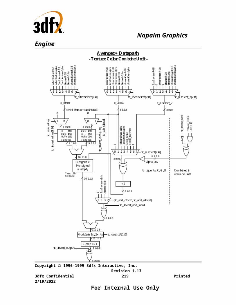
Napalm Graphics Engine
17.5 miscInit0 Register (0x10)miscInit0 contains resets to all subsystems, pixel swizzling, and Y origin subtraction. Bits [1:0] reset the 3D graphics subsytem. Bits [3:2] enable byte/word swizzling during register accesses to 2D or 3D. Bits [6:4] define resets for video, 2D, and memory subsytems. Bits[29:18] define the Y origin subtraction value used during address calculation when Y flip is enabled in fbzMode. Bits [31:30] enable byte/word swizzling during non modal LFB reads and writes
Bit DescriptionMiscellaneous Control
0 FBI Graphics Reset (0=run, 1=reset). Default is 0.1 FBI FIFO Reset (0=run, 1=reset). Default is 0. [resets PCI FIFO and the PCI data
packer]3:2 reserved4 Video Timing Reset (0=run, 1=reset). Default is 0.5 2D Graphics Reset (0=run, 1=reset). Default is 0.6 Memory Timing Reset (0=run, 1=reset). Default is 0.7 VGA Video Timing Reset (0=run, 1=reset). Default is 0.10:8 Programmable delay to be added to the blank signal before it outputs to the TV out
interface. This is in terms of number of flops clocked by the 2x clock. The objective is to synchronize the blank signal with the data output by matching the CLUT delay. Default is 0x0. 000 = 2 flops; 001 = 3 flops; …… 111 = 9 flops
13:11 Programmable delay to be added to the vsync and hsync signals before they are output to the TV out interface. This is in terms of number of flops clocked by the 2x clock. The objective is to synchronize the sync signals with the data output by matching the CLUT delay. Default is 0x0.000 = 2 flops; 001 = 3 flops; …… 111 = 9 flops
16:14 Programmable delay to be added to the vsync and hsync signals before they are output to the monitor. This is in terms of number of flops clocked by the 2x clock. The objective is to synchronize the sync signals with the data output by matching the delay through the CLUT and DAC. Default is 0x0.000 = 2 flops; 001 = 3 flops; …… 111 = 9 flops
17 ReservedY Origin Definition bits
29:18 Y Origin Swap subtraction value (12 bits). Used when renderMode[2] = 0. Default is 0x0.
30 miscInit1 address space alias control (0=accesses to miscInit1 address space access the miscInit1 register, 1=accesses to miscInit1 address space access the vip2vmiCtrl register). Default is 0.
31 VMI host port control (0=VMI host port controlled by vidSerialParallelPort bits{(17:14), (13:6),(3:1)}, 1=VMI host port controlled by queued 3D lfb writes with lfb write format = 0x9). Default is 0.
Copyright 1996-1999 3dfx Interactive, Inc. Revision 1.133dfx Confidential 219 Printed 5/7/2023
For Internal Use Only

Napalm Graphics Engine
17.6 miscInit1 Register (0x14 when miscInit0[30]=0)miscInit1 register controls miscellaneous operations of Napalm available in real mode. Bit 0 is used to correct for CLUT addresses being inverted during host accesses. This bit should be set to 1 for proper operation. Bit 3 enables and disables writes to the PCI subVendorID and subSystemID registers. Bit 4 enables writes to the ROM through romBaseAddr. Bit 5 enables the new triangle address aliasing allowing better address compaction. Bit 6 disables texture mapping.
Power down of Napalm is controlled by bits 11:7, where bit 7 powers down the color lookup tables, bit 8 powers down the DAC itself, bits 9, 10, and 11 power down the three PLL’s.
Bits 17 and 18 disable stalling on the opposite pipe (either 2D or 3D) when a command is sent down. These bits are used for testing, and should not be set during normal operation.
Bit 19 is used to terminate command fifo activity. Setting this bit to ‘1’ halts the command fifo and resets all of the registers in the command register space to their default values. In order for Napalm to be shut down gracefully, this bit should only be set when Napalm is idle. Be sure to restore this bit to 0 when finished.
Bits 28 through 24 indicate the value of the strapping registers at boot up. Note that altering these bit effect the read back information of PCI and AGP resource reporting. For more information on the strapping registers, see the section on Power on Strapping.
miscInit1 bits(22:20) control the byte swizzling and word swapping capabilities for the memBaseAddr1 address space. When miscInit1[22]=1, then the address bits selected by miscInit1[21:20] control the type of byte swizzling and word swapping performed on all reads and writes to and from memBaseAddr1 as follows:
Selected address bits
Description
00 No swapping. pciData[31:0] pciData[31:0]01 Byte swapping. pciData[31:0] {pciData[7:0], pciData[15:8],pciData[23:16],
pciData[31:24]}10 Word swapping. pciData[31:0] {pciData[15:8], pciData[7:0],pciData[31:24],
pciData[23:16]}11 Byte and Word swapping. pciData[31:0] {pciData[23:16],
pciData[31:24],pciData[7:0], pciData[15:8]}
Copyright 1996-1999 3dfx Interactive, Inc. Revision 1.133dfx Confidential 220 Printed 5/7/2023
For Internal Use Only
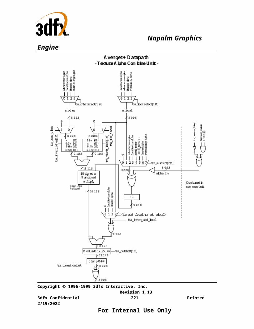
Napalm Graphics Engine
Bit DescriptionMiscellaneous Control
0 invert_clut_address. Default = 0.2:1 tri_mode – triangle iterator mode. Default is 0x0.3 Enable Sub Vendor/ Subsystem ID writes. (0=disable, 1=enable). Default is 0x0.4 Enable ROM writes. (0=disable, 1=enable). Default is 0x0.5 Alternate triangle addressing map (0=disable, 1=enable). Default is 0x0.6 Disable texture mapping (0=enable, 1=disable). Default is 0x0.
Power Down Control7 Power Down CLUT. Default is 0x0.8 Power Down DAC. Default is 0x0.9 Power Down Video PLL. Default is 0x0.10 Power Down Graphics PLL. Default is 0x0.11 Power Down Memory PLL. Default is 0x0.
2D Block Write Control14:12 Block write threshold. Default is 0x0.15 Disable 2D Block write. Default is 0x0.16 Disable 2D stall on 3D synchronous dispatch. When set to 1, 2D will not wait on
pending 3D operations to complete before being issued. Default is 0x0.17 Disable 3D stall on 2D synchronous dispatch. When set to 1, 3D will not wait on
pending 2D operations to complete before being issued. Default is 0x0.18 Disable broadcast of all TMU registers to both TMUs when 2 pixel-per-clock operation
is enabled. (1=disable).19 Command Stream Reset (1=reset command streams, 0 = normal operation). Default is
0x0.21:20 Byte swizzle all reads and writes to and from memBaseAddr1 address space address
select control:0=pciAddr[29:28] is used to select byte swizzling algorithm (4 aliases of 256MBytes of frame buffer memory, each with unique byte swizzling),1=pciAddr[28:27] is used to select byte swizzling algorithm (4 aliases of 128MBytes of frame buffer memory, each with unique byte swizzling),2=pciAddr[27:26] is used to select byte swizzling algorithm (4 aliases of 64MBytes of frame buffer memory, each with unique byte swizzling),3=pciAddr[26:25] is used to select byte swizzling algorithm (4 aliases of 32MBytes of frame buffer memory, each with unique byte swizzling)
Default is 0.22 Byte swizzle all reads and writes to and from memBaseAddr1 address space enable
(1=enable). Default is 0.23 Reserved24 PCI Fast device. Default strapped on VMI_DATA 025 PCI BIOS Size. Default strapped on VMI_DATA 126 PCI 66Mhz. Default strapped on VMI_DATA 2.27 AGP Enabled. Default strapped on VMI_DATA 3.28 PCI Device Type. Default strapped on VMI_DATA 4.29 pd pin value (input value of the pd pin). Default is 0.31:30 pd signal control (0,1=tristate, 2=drive low, 3=drive high). Default is 0x0.
Copyright 1996-1999 3dfx Interactive, Inc. Revision 1.133dfx Confidential 221 Printed 5/7/2023
For Internal Use Only
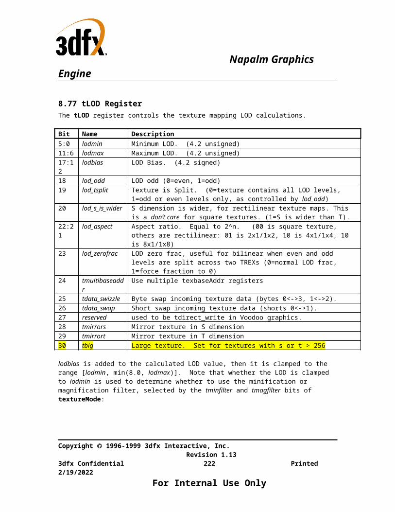
Napalm Graphics Engine 17.7 vip2vmiCtrl Register (0x14 when miscInit0[30]=1)vip2vmiCtrl controls the VIP-to-VMI translation module in Napalm. The default value is 0x80001. Note that vip2vmiCtrl is accessed by setting miscInit0[30] and accessing the miscInit1 register. When miscInit0[30]=1, then accesses to miscInit1 register will instead be directed to vip2vmiCtrl.
Bit Description0 VIP-to-VMI disable (0=enable VIP-to-VMI translation, 1=passthru VMI signals
unmodified). Default is 1.1 vbi_int (1=enable interrupt at end of VBI lines). Default is 0.2 vbi_crop (1=enable VBI cropping). Default is 0.3 reserved8:4 vbi_max[4:0]. Default is 0.18:9 vid_max[9:0]19 Reset vip2vmi module (1=reset module). Default is 1.29:20 reserved30 reserved (for Write accesses)30 vip2vmi_intr_field (for Read accesses)31 Enable VIP-to-VMI translation (1=enable, for Write accesses). Default is 0.31 vip2vmi_intr_type (for Read accesses)
When vbi_int (vip2vmiCtrl[1]) is set, it enables an interrupt at the end of the VBI lines. A rising edge on vmi_intr will be generated at earliest of either the EAV of the first line without the “V” bit set in the SAV code or the EAV of that last line as defined by the VBI_MAX counter. (Note the V and F bits is EAV/SAV only change at EAV. The EAV has the codes for the next line.) This function is independent of the crop bit below. It is possible to have the VBI interrupt enabled and crop the VBI data over the port.
When vbi_crop (vip2vmiCtrl[2]) is set, vmi_vact will not be active for any lines with “V” set its EAV/SAV code. This crops the VBI data.
The vbi_max field (vip2vmiCtrl[8:4]) contains the number of lines with the “V” bit set in EAV/SAV that will have VMI_VACT active during its valid pixel period. Any additional lines will be cropped.
The vid_max field (vip2vmiCtrl[18:9] contains the number of lines with the “V” bit clear in EAV/SAV that will have VMI_VACT active during its valid pixel period. Any additional lines will be cropped.
vip2vmiCtrl bits[31:30] have different definitions when they are written as opposed to when they are being read. When read, vip2vmi_intr_field (vip2vmiCtrl[30]) is the state of the “F” bit in the last EAV code before VMI_INTR went active. Also when read, vip2vmi_intr_type (vip2vmiCtrl[31]) is set if the last VMI_INTR was for VBI data and cleared if the last VMI_INTR was for non VBI data. When written, vip2vmiCtrl[30] is a reserved bit and vip2vmiCtrl[31] should be set for VIP-to-VMI translation.
Note that vip2vmiCtrl[0] must be cleared, vip2vmiCtrl[19] must be cleared, and vip2vmiCtrl[31] must be set in order for proper VIP-to-VMI translation to occur. When VMI video port is desired, vip2vmiCtrl[0] should be set, vip2vmiCtrl[19] should be set, and vip2vmiCtrl[31] should be cleared (this is the poweron default state).
17.8 dramInit0 Register (0x18)dramInit0 controls the sgram interface timing of specific timing parameters. The default value of this register is 0x00579d29.
Copyright 1996-1999 3dfx Interactive, Inc. Revision 1.133dfx Confidential 222 Printed 5/7/2023
For Internal Use Only
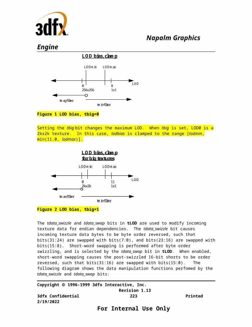
Napalm Graphics Engine Bit Description
Sgram access timing1:0 tRRD – row active to row active (1-4 clks). Default is 0x1 (2 clks)3:2 tRCD – RAS to CAS delay (1-4 clks). Default is 0x2 (3 clks).5:4 tRP – row precharge (1-4 clks). Default is 0x2 (3 clks).9:6 tRAS – minimum active time (1-16 clks). Default is 0x4 (5 clks).13:10 tRC – minimum row cycle time (1-16 clks). Default is 0x7 (8 clks).15:14 tCAS latency (1-4 clks). Default is 0x2 (3 clks).16 tMRS mode and special mode register cycle time (1-2 clks).. Default is 0x1 (2 clks)17 tDQR Rd to DQM assertion delay (0-1 clks). Default is 0x1 (1 clk)18 tBWC Block write cycle time (1-2 clks). Default is 0x1 (2 clks)19 Napalm: tWL WR to pre (1-2 clks). Default is 0x0 (1 clk).
Napalm2: tWL WR to pre (1-4 clks). tWL is formed by {dramInit0[31],dramInit0[19]}. Default is 0x0 (1 clk).
21:20 tBWL BKWR to Pre (1-4 clks). Default is 0x1 (2 clks)22 Napalm: tRL RD to PRE (1-2 clks). Default is 0x1 (2 clks)
Napalm2: tRL RD to PRE (1-4 clks). tRL is formed by {dramInit1[31],dramInit0[22]}. Default is 0x1 (2 clks).
23 dont allow WR/BKWR to terminate RD, use BST. Default is 0x0 (allow wr-term)24 Disable the dead bus cycle btw. RD and WR (0=enable, 1=disable). Default is 0x025 SGRAM write per bit enable (0=disable, 1=enable). Default is 0x026 Number of Sgram/Sdram chipsets (0=1, 1=2). Default is power on strap
VMI_DATA_5.29:27 Sgram/Sdram type (0=8Mbit, 1=16Mbit, 2=32Mbit, 3=64Mbit, 4=128Mbit). Default is
power on strap {TV_DATA_3, TV_DATA_2, VMI_DATA_6})30 mctl_dram_numbanks – number of sgram/sdram internal banks (0=2 internal banks,
1=4 internal banks). Default is power on strap TV_DATA_4.31 Napalm: reserved.
Napalm2: tWL WR to pre (1-4 clks). tWL is formed by {dramInit0[31],dramInit0[19]}. Default is 0x0 (1 clk).
Copyright 1996-1999 3dfx Interactive, Inc. Revision 1.133dfx Confidential 223 Printed 5/7/2023
For Internal Use Only
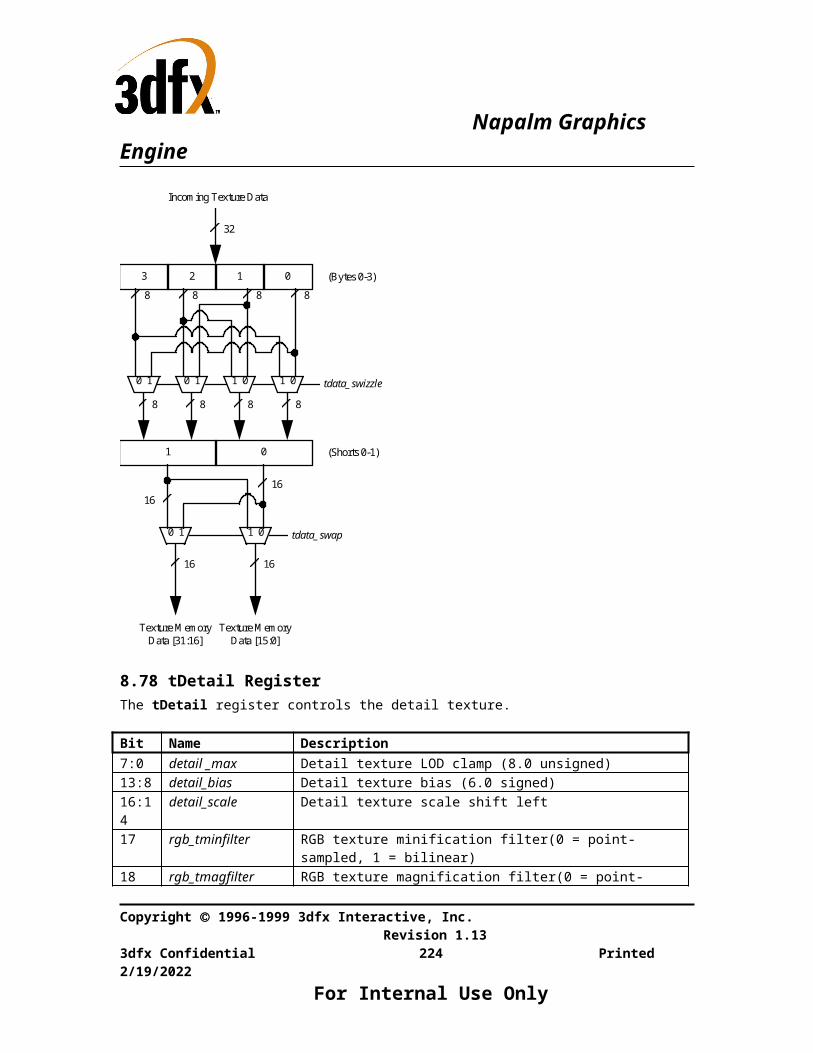
Napalm Graphics Engine
17.9 dramInit1 Register (0x1C)Bit Description
SGRAM Refresh Control0 Refresh Enable (0=disable, 1=enable). Default is 0.9:1 Refresh_load Value. (Internal 14-bit counter 5 LSBs are 0x0) Default is 0x100.
Video Refresh Control10 Video arbitration priority. (0=normal, 1=aggressive) Default is 0
Miscellaneous video Control11 Triple buffer enable (0=double buffering, 1=triple buffering). Default = 0.12 Reserved. Default = 0.
SGRAM read data sampling control13 sg_clk_nodelay – bypass the delay element. Default = 1.14 sg_use_inv_sample – resample the flopped sgram data with another negative-edge flop
before flopping data with mclk. Default = 0.15 sg_del_clk_invert – invert delayed clock before using it. Default = 0.19:16 sg_clk_adj – delay value for sgram read data sample clock. Default = 0x0. (2-62
NAND gates of delay, in steps of 4)SGRAM frame buffer output delay control (control + data bits)
23:20 sg_oflop_del_adj – delay value for mclk (2-62 nand gates of delay, in steps of 4) to transparent latch that sends fb_* off chip. Default = 0xf.
24 sg_oflop_trans_latch – forces latch for fb_* signals to be transparent. (0=use delayed mclk to latch, 1=make latch always transparent). Default = 0.Memory Controller configuration bits
25 mctl_short_power_on. Power on in 128 cycles. Default = 0. VMI_ADDR_126 mctl_no_aggressive – turn off mem_ctrl’s aggressive row activation. Default = 0.27 mctl_pagebreak – force a pagebreak for all accesses. Default = 0.28 mctl_tristate_outputs – force data outputs to be tristate. Default = 0.29 mctl_no_vin_locking – prevent vin from locking the bus during requesting. 0=allow
locking, 1=prevent locking. Default = 0.30 Rev. B0 and after: mctl_type_sdram – (0=use SGRAMs, 1=use SDRAMs). Default = 0.
VMI_ADDR_231 Napalm: reserved.
Napalm2: tRL RD to PRE (1-4 clks). tRL is formed by {dramInit1[31],dramInit0[22]}. Default is 0x1 (2 clks).
When using SGRAMs, mctl_type_sdram should be set to 0. When using SDRAMs, only 16Mbit (16x512K parts) are supported, which result in a 16MB frame buffer. The sgram_type and sgram_chipsets bits in dramInit0 are ignored when mctl_type_sdram=1.
Rev. B0 and after: Note that the fastfillCMD behaves differently when mctl_type_sdram=1 (dramInit1[30]). When fastfilling with SGRAMs (mctl_type_sdram=0), if dithering is enabled and fastfillCMD[0]=1, no dithering will happen. But when fastfilling with SDRAMs (mctl_type_sdram=1), if dithering is enabled and fastfillCMD[0]=1, dithering will still happen, since SDRAMs do not support blockwriting.
Copyright 1996-1999 3dfx Interactive, Inc. Revision 1.133dfx Confidential 224 Printed 5/7/2023
For Internal Use Only
Napalm Graphics Engine 17.10 agpInit0 Register (0x20)The agpInit0 register is used to control how AGP behaves when making requests. Bit 0 sets the request priority level. Bits [3:1] are now reserved. Bits [6:4] determine when the agp request fifo becomes full (requests that have not yet been issued to the AGP target). Bits [10:7] control when to much data has been returned, and AGP needs to begin stalling. Bits 31:27 allow for active outstanding AGP requests to be monitored. the Value 0x1f indicates no outstanding requests, while 0x0 indicates 17 outstanding requests.
Bit Description0 Force AGP request to be high priority. (0=Low, 1 = High). Default is 0x0.3:1 Reserved.6:4 AGP request fifo full threshold. Default is 0x1.10:7 AGP read fifo full threshold. Default is 0x9.26:10 Reserved. Defaults is 0x0.31:27 AGP Requests Outstanding. (Read Only)
17.11 tmuGbeInit Register (0x24)tmuGbeInit register contains the fifo water marks for both the TMU and FBI sections. The default value of this register is 0x0bfb. Bits [19:15] control the delay (with a NAND chain) of the TV-Out output clock. Bits [24:20] control the delay (with a NAND chain) of the AA-data bus output clock.
Bit Description3:0 Texture read request low water mark - fifo freespace level that TMU will empty the
read request queue to before stopping a sequence. Default is 0xb.7:4 Texture read request high water mark - fifo freespace level at which TMU will start a
sequence. Default is 0xf.11:8 Pixel fifo high water mark – fifo freespace level at which FBI will start a sequence.
Default is 0xf.12 txc_disable_rdrq_max – disable the limit of 16 as the max limit of max number of
reads in a row by the texture cache interface to the memory controller. Default = 0.13 txc_use_min_req - sets the minimum number of reads done by the texture cache to 3.
Default = 0.14 txc_force_cam_miss. Default = 0.
TV Out clock delay adjust15 tv_out_clk_inv - invert delayed clock. Default = 0.19:16 tv_out_clk_del_adj – choose between 16 values of delay. Default = 0.
AA clock delay adjust20 aa_clk_inv – invert delayed clock. Default = 0.24:21 aa_clk_del_adj – choose between 16 values of delay. Default = 0.
Memory Interface Control (Napalm2 only)27:25 mctl_memory_port_config (0=64-bit DDR, 1=reserved, 2=32-bit DDR, 3=reserved,
4=64-bit SDR, 5-7=reserved). Default is power on strap {TV_DATA_9, TV_DATA_8, TV_DATA_7}.
31:28 Reserved
Copyright 1996-1999 3dfx Interactive, Inc. Revision 1.133dfx Confidential 225 Printed 5/7/2023
For Internal Use Only
Napalm Graphics Engine 17.12 vgaInit0 Register (0x28)The vgaInit0 register is used for hardware initialization and configuration of the VGA controller in Napalm. VGA can be disabled by writing bit 0 to a “1”. Bit 1 allows external video timing to drive the VGA core video scan out logic. Bit 2 controls how the VGA DAC control logic views the width of the RAM. For VGA compatibility, this bit should be set to 0 (6 bit DAC).
VGA extensions are enabled by bit 6. These extensions are mention in the VGA portion of this spec, in the CRTC register space. Bit 10 enables the ability to read back the PCI configuration when bit 6 of this register is 0.
Bit 8 determines if the chips should wake up as a VGA motherboard or an add in card. Bit 9 disables the VGA to response to legacy address decoding. This bit should be set if Napalm is not the primary display adapter in the system. Setting this bit also disables write access to 0x46e8 and 0x102.
Bit 12 should be set when in an extended (non-VGA) mode. This disables the VGA from fetching memory data during video raster scan out.
Bit 13 is used when an external DAC is supported. This bit should always be set to 0.
Bits(24:23) and bits(21:14) determine the start page of VGA in board memory. The 26-bit starting address of VGA in memory is formed as {vgaInit0[24:23], vgaInit0[21:14], 0000_0000_0000_0000}. By default, VGA is placed at the beginning of memory. If need be, it can be moved anywhere on a 64K byte boundary within 64M bytes.
Bit 22 disables VGA refresh control of board memory. When VGA is in scan out mode, it prefers memory refresh to happen at horizontal sync time. When this bit is set to 0, three memory refresh cycles happen after HBLANK occurs, and the memory refresh time out counter is deferred. When this bit is set to 1, the memory refresh time out counter explicitly controls memory refresh events.
Copyright 1996-1999 3dfx Interactive, Inc. Revision 1.133dfx Confidential 226 Printed 5/7/2023
For Internal Use Only
Napalm Graphics Engine
Bit Description DefaultMiscellaneous Control
0 VGA disable. (0=Enable, 1 = Disable). Setting this bit to 1 shuts off all access to the VGA core. Default is poweron strapping value FB_DATA_21.
FB_DATA_21
1 Use external video timing. This bit is used to retrieve SYNC information through the normal VGA mechanism when the VGA CRTC is not providing timing control.
0
2 VGA 6/8 bit CLUT. (0= 6 bit, 1 = 8 bit). 13 Disable internal vga_valid_mem_address and vga_valid_io_address
signals in pci decoder. Default is poweron strapping value FB_DATA_23.
FB_DATA_23
5:4 Reserved. 0x06 Enable VGA Extensions 07 VGA Memory re-map enabled. This bit is used for test purposes.
When set, VGA can be rem-mapped into MEMBASE0 + 0x0aa0000 to MEMBASE0+0xabffff.
0
8 0x46e8/0x3C3 Wake up select (0=use 0x46e8, 1=use 0x3C3 or IO Base + 0xC3). VGA add in cards that use 0x46e8 while mother board VGA uses 0x3C3. When Napalm is a multimedia device, this bit should be set to ‘1’ and the VGA subsystem should be enabled with IO Base + 0xC3. Default is poweron strapping value FB_DATA_22.
FB_DATA_22
9 Disable VGA Legacy Memory/IO Decode (0=Enable, 1=Disable). Default is poweron strapping value FB_DATA_22.
FB_DATA_22
10 Use alternate VGA Config read back (0 = Enable, 1=Disable). Setting this bit to 0 allows the VGA to read back configuration through CRTC index 0x1c.
0
11 Enable Fast Blink (test bit) (1=fast blink, 0 = normal blink). 0x012 Use extended video shift out. Set this bit to 1 to disable all VGA
memory access when video processor is shifting out data.0
13 Decode 3c6. (test bit) 021:14 VGA base offset, bits (7:0), specified in 64k quantities. 022 Disable SGRAM refresh requests on HBLANK. When set to 1, the
VGA does not produce memory refreshes during horizontal blanking.1
24:23 VGA base offset, bits (9:8), specified in 64k quantities. 025 VBE read Aperture, bit 10, specified in 32K quantities. 026 VBE read Aperture, bit 11, specified in 32K quantities. 031:27 reserved 0
17.13 vgaInit1 Register (0x2C) The vgaInit1 register contains the read and write apertures for VBE. VBE uses address 0xA0000 as an aperture into Napalm memory. See the section on VBE apertures in the VGA portion of this document. Bit 20 enables sequential chain mode, a pseudo packed pixel format Bits 28:21 define lock bits that disable writes to specific sections of the VGA core. See the section on register locking in the VGA portion of this document.
Copyright 1996-1999 3dfx Interactive, Inc. Revision 1.133dfx Confidential 227 Printed 5/7/2023
For Internal Use Only
Napalm Graphics Engine
Bit Description Default9:0 VBE write Aperture, bits (9:0), specified in 32K quantities 019:10 VBE read Aperture, bits (9:0), specified in 32K quantities. 020 Enable 0xA0000 Sequential Chain 4 mode. 021 Lock Horizontal Timing - 3B4/3D4 index 0,1,2,3,4,5,1a 022 Lock Vertical Timing -3B4/3D4 index 6,7 (bit 7,5,3,2 and 0), 9 10, 11
(bits[3:0]), 15,16,1b.0
23 Lock H2 - 0x3B4/0x3D4 index 17, bit 2 024 Lock Vsync - 0x3C2, bit 7. 025 Lock Hsync - 0x3C2, bit 6. 026 Lock Clock Select - 0x3C2, bits 3 and 2. 027 Lock Ram Enable - 0x3C2, bit 1 028 Lock Character Clock - 0x3C4, index 1 bit 0. 029 VBE write Aperture, bit 10, specified in 32K quantities. 030 VBE write Aperture, bit 11, specified in 32K quantities. 031 reserved 0
17.14 2d_Command_Register (0x30)Writing to this register is the same as writing to the 2d unit’s command register. This mapping is intended to provide a way to initialize the SGRAM mode and special mode registers at init time.
17.15 2d_srcBaseAddr Register (0x34)Writing to this register is the same as writing to the 2d unit’s srcBaseAddr register. This mapping is intended to provide a way to initialize the SGRAM mode and special mode registers at init time.
17.16 strapInfo Register (0x38) The strapInfo register is used to access values from the power-on strapping pins. There are 2 strapInfo registers: strapInfo0[31:0] and strapInfo1[31:0]. Writing to bit(0) of strapInfo selects which strapInfo register will be returned when a read is performed from strapInfo. After a write to strapInfo is performed with bit(0)=0, then all subsequent reads from strapInfo will return the value from the strapInfo0 register. Similarly, after a write to strapInfo is performed with bit(0)=1, then all subsequent reads from strapInfo will return the value from the strapInfo1 register. See the section on “Power On Strapping Pins” for the default values and bit descriptions of strapInfo0 and strapInfo1.
17.17 iMatchCtrl Register (0x48)The iMatchCtrl register is used to control the impedance matching of the AGP I/O. Bit 0 enables the update mechanism for the I/O. Bit 1 enables the bypass mechanism.
When bit 1 is set to 1, values can be programmed into bits [11:8] and bits[15:12] for the N and P balancing, respectivley. When this bit is a 0, the values for bit [11:8] and [15:12] are read only.
If the device is in PCI or AGP 2X modes, the value is hardwired in the control logic.
If the device is in AGP 4X mode and bit 0 is set to 1, the device measures the impedence on two dedicated pins. Subsequent reads to this register (bit 0 is still 1) cause the 4 bit N and P values to be
Copyright 1996-1999 3dfx Interactive, Inc. Revision 1.133dfx Confidential 228 Printed 5/7/2023
For Internal Use Only
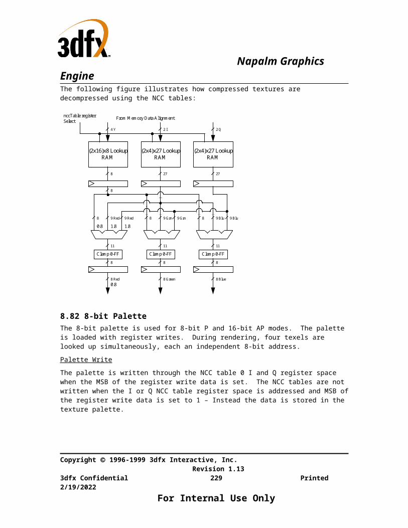
Napalm Graphics Engine
broadcast to the I/O. This allows adequate settling of the new N and P values without allowing bad data transfers.
Bits [31:16] are a the value for the iMatchCtrl count down timeout counter, in Vsync times. This allows for a very large interval to occur for generating interrupts. In general, these bits should be used to indicate to hardware that is is time to update this register (every five to ten minutes). The counter is used in conjuction with the intrCtrl register bit 24 and 25 to generate INTA# interupts on the PCI bus. The actual values programmed in this register are important only in that the register is updated frequently enough to counter system impedance changes due to voltage or temperature drift.
Bit Description0 Enable Measure logic. (0=disable, 1 = enable). Default is 0x0.1 Bypass Mode. (0=use internal values, 1 = use programmed values)7:2 Reserved. Defaults is 0x0.11:8 PAD N value. Default is determined by mode.15:12 PAD P value. Default is determined by mode.31:16 iMatchCtrl Interrupt counter.
18. Frame Buffer Access
18.1 Frame Buffer OrganizationThe Napalm linear frame buffer base address is located in a separate memory base address register in PCI config space and occupies 128 megabytes of address space for linear access. Linear memory starts at the beginning of Sgram memory and finishes at the begin of tiled memory specified by the tilebase register in init register space. It is assumed (but not required) that VGA will use the first 256K of linear memory, and the desktop, video, and textures will use the remaining linear memory.
18.2 Linear Frame Buffer AccessLinear frame buffer access is accessed much like system, and can store the desktop, video, 3D front buffer, 3D back buffer, 3D auxiliary buffer, and textures. Memory management is done with a true linear memory manager.
Copyright 1996-1999 3dfx Interactive, Inc. Revision 1.133dfx Confidential 229 Printed 5/7/2023
For Internal Use Only
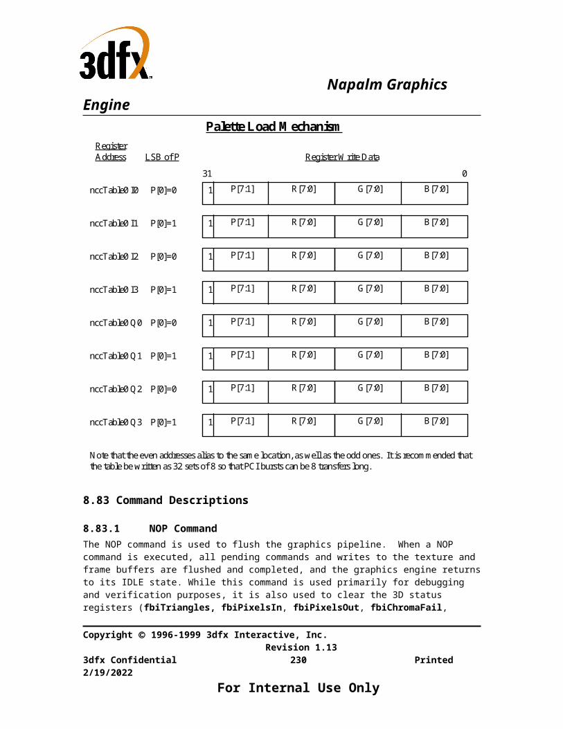
Napalm Graphics Engine
18.3 Tiled Frame Buffer AccessTiled frame buffer access is a rectilinear memory based on 128 byte x 32 line tiles. Tiled memory is suited for 3D performance, where localized access is needed. Tiled frame buffer access is done with a concatenation of Y and X much like the 3D linear frame buffer access, and the frame buffer access of SST1. Tiled frame buffer Access is defined by writing the beginning tile/page into the tiled base address register. When configuring tiled frame buffer access, it is best to set the global tile stride to the largest surface width for best memory management. Memory management for tiled memory must be done by a rectilinear memory manager. Access to tiled memory is shown below. It is recommended that tiled memory be used sparingly since this memory fragments very easily, and utilization will not be 100%.
21 43 65 87
109 1211 1413 1615
1817 2019 2221 2423
2625 2827 3029 3231
3433 3635 3837 4039
4241 4443 4645 4847
Tiled Memory One Tile
128 bytes x 32 lines
1024bytes x 192lines
Copyright 1996-1999 3dfx Interactive, Inc. Revision 1.133dfx Confidential 230 Printed 5/7/2023
For Internal Use Only

Napalm Graphics Engine This is the PCI to XY calculation
PCI Offset to XYbyte conversion
1K byte stride
Y[14:0], X[9:0] [24:0]
2K byte stride
Y[13:0], X[10:0] [24:0]
4K byte stride
Y[12:0], X[11:0] [24:0]
8K byte stride
Y[11:0], X[12:0] [24:0]
16K byte stride
Y[10:0], X[13:0] [24:0]
The following is the page calculation that must be used in the base address registers in video, 3D, 2D, and texture units.
Page equation = (X / 128) + basepage + (Y / 32) * tilestride.
: Where X is referenced in bytes, and Y is referenced in lines.
19. YUV Planar Access YUV planar memory allows the CPU to write Y, U, and V in separate regions of memory space. As Y, U, and V are written, they are converted into YUYV packed form, and stored in the frame buffer at the correct offset from the YUV base address register. The first megabyte region defines Y, where each 32-bit write, generates a 64-bit write on Napalm, with appropriate byte masks. The second megabyte region of YUV planar memory defines U space, where each 32-bit write generates two 64-bit writes with appropriate byte enable bits. The third region of YUV planar memory defines the V space, where each 32-bit write generates two 64-bit writes with appropriate byte enable bits. The conversion between planar and packed is described below. YUV planar space has a fixed 1024 byte stride, and a programmable destination stride.
Copyright 1996-1999 3dfx Interactive, Inc. Revision 1.133dfx Confidential 231 Printed 5/7/2023
For Internal Use Only
Napalm Graphics Engine
0xC00000
0xD00000
0xE00000
Y
U
V
Y8
Y0 Y1
Y9 Y10
Y2 Y3
Y11
Y24
Y16 Y17
Y25 Y26
Y18 Y19
Y27
Y12
Y4 Y5
Y13 Y14
Y6 Y7
Y15
Y28
Y20 Y21
Y29 Y30
Y22 Y23
Y31
Y40
Y32 Y33
Y41 Y42
Y34 Y35
Y43
Y56
Y48 Y49
Y57 Y58
Y50 Y51
Y59
Y44
Y36 Y37
Y45 Y46
Y38 Y39
Y47
Y60
Y52 Y53
Y61 Y62
Y54 Y55
Y63
U4
U0 U1
U5 U6
U2 U3
U7
U12
U8 U9
U13 U14
U10 U11
U15
V4
V0 V1
V5 V6
V2 V3
V7
V12
V8 V9
V13 V14
V10 V11
V15
0 1 2 3 4 5 6 7 8 9 10 11 12 13 14 15
Y0 U0 Y1 V0 Y2 U1 Y3 V1
Y8 U0 Y9 V0 Y10 U1 Y11 V1
Y4 U2 Y5 V2 Y6 U3 Y7 V3
Y12 U2 Y13 V2 Y14 U3 Y15 V3
Y16 U4 Y17 V4 Y18 U5 Y19 V5
Y24 U4 Y25 V4 Y26 U5 Y27 V5
Y20 U6 Y21 V6 Y22 U7 Y23 V7
Y28 U6 Y29 V6 Y30 U7 Y31 V7
Y32 U8 Y33 V8 Y34 U9 Y35 V9
Y40 U8 Y41 V8 Y42 U9 Y43 V9
Y36 U10 Y37 V10 Y38 U11 Y39 V11
Y44 U10 Y45 V10 Y46 U11 Y47 V11
Byte #
YUV Planar space
Banshee Frame buffer
Copyright 1996-1999 3dfx Interactive, Inc. Revision 1.133dfx Confidential 232 Printed 5/7/2023
For Internal Use Only
Napalm Graphics Engine
20. Texture Memory Access
! New for AVENGER: Avenger and Napalm require special flushing to be done surrounding texture downloads. Please see section 19.3 for more information.
There are two methods of storing textures: (1) a single base address for all LODs within a texture or (2) multiple base addresses. With method (1), textures are stored as if mipmapped, even for textures containing only one level of detail. The largest texel map (LOD level 0) is stored first, and the others are packed contiguously after; for tiled space, successive LODs after 0 are stored in a manner that groups the LODs into a somewhat rectangular space; more on this later. When only some or one of the LOD levels are used, lodmin and lodmax are used to restrict texture lookup to the levels that were loaded.
With method (2), multi-base address mode, texbaseaddr points to where LOD level 0 starts and texbaseaddr1, texbaseaddr2, and texbaseaddr38 point to where LOD levels 1, 2, and 3-8 start, respectively. This mode provides more granularity to texture storage, and can help texture memory allocation. There is only one base address for mipmaps 3-8, so these are stored contiguously.
Texture memory can be defined as either linear or tiled, as defined by the appropriate bit in texbaseaddr.
When in single base address mode, texbaseaddr points to where the texture would start if it contained LOD level 0 (256x* dimension). As described above, all LODs are stored contiguously after the first.
Addresses are generated by adding texbaseaddr and an offset that is a function of LOD, S, T, tclamps, tclampt, tformat, lod_aspect, lod_s_is_wider, trexinit0, trexinit1. texbaseaddr can be set below zero, such that the offset to the texture wraps to a positive number.
20.1 Writing to texture spaceNapalm provides a dedicated texture download port which is synchronized with normal rendering. Texturedownloads done through this port are guaranteed to be processed in-order with 3d rendering, which alleviates the host from having to idle the chip before downloading. The texture port allows writing to frame buffer memory within a 4 byte aligned region.
The Napalm texture download port occupies 2 Mbytes of PCI address space as shown in section 4.. Note that only writes are supported through the texture download port; reads to this area return undefined data. Texture space can also be accessed (in a non-synchronized fashion) through the LFB port, which provides both read and write accesses.
Texture downloads through the texture download port are always texbaseaddr-relative, even in multi-base address mode. texbaseaddr1, texbaseaddr2, and texbaseaddr38 are unused during such downloads.
Copyright 1996-1999 3dfx Interactive, Inc. Revision 1.133dfx Confidential 233 Printed 5/7/2023
For Internal Use Only
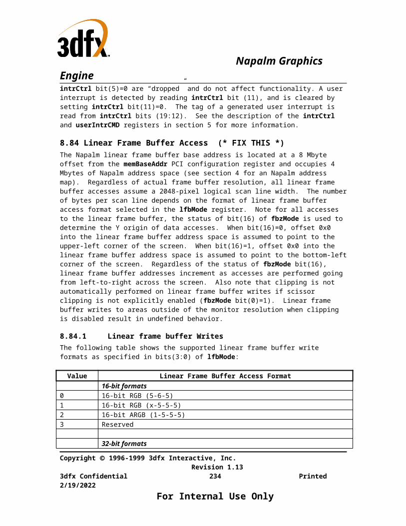
Napalm Graphics Engine
LOD 0
LOD 1
LOD 2LOD 3-8
FrameBufferSpace
texbaseaddr
linear texture space
tiled texture space
LOD 0LOD 2
LOD 1
LOD 3-8
texbaseaddr
LODs 3-8
LOD3
LOD4
LOD5
LODs6, 7, 8
Copyright 1996-1999 3dfx Interactive, Inc. Revision 1.133dfx Confidential 234 Printed 5/7/2023
For Internal Use Only

Napalm Graphics Engine
Copyright 1996-1999 3dfx Interactive, Inc. Revision 1.133dfx Confidential 235 Printed 5/7/2023
For Internal Use Only
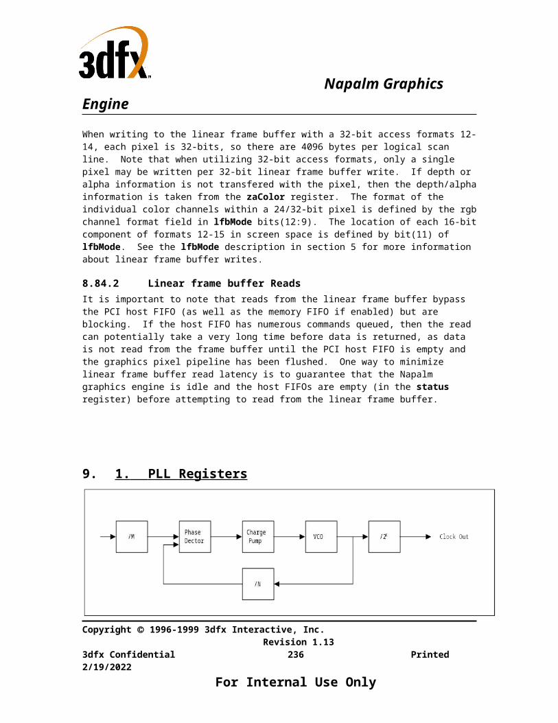
Napalm Graphics Engine
Copyright 1996-1999 3dfx Interactive, Inc. Revision 1.133dfx Confidential 236 Printed 5/7/2023
For Internal Use Only

Napalm Graphics Engine
20.2 Calculating texel addressesWhen downloading textures through the texture download port, a different scheme of address translation is applied, depending on whether the texture memory space is in tiled or linear space.
Lineartexture download aperture address definition25 0offset[25:0]
In linear texture space, texels are packed totally linearly starting from the base address. Any texel can be referenced by using this equation:
lfb_texel_addr[23:0] = ({texbaseaddr[1],texbaseaddr[24:4], 4’h0} + lod_offset[17:0] + s + t*lod_width);
(lod_offset[17:0] is the offset of the given mipmap level from the base address)
Example: Calculate the physical address for texel 30,45 in LOD 2, with aspect=1x1, 16bpp texels, and a texbaseaddr = 0x200000; assume that LODs 0,1 exist and that we are non-multi base addr.:lfb_phys_addr[23:0] = (0x200000 + size_lod_0 + size_lod_1 + (30 + 45 * 64)*2);
= (0x200000 + (256*256*2) + (128*128*2) + (30+45*64)*2);= 0x2296bc;
offset[20:0] = lfb_phys_addr[20:0] = 0x296bc;
You could download to this texel by setting texbaseaddr to 0x200000 and then writing to the lower (s is even) 16 bits of this pci address:pci_addr[23:0] = (0x600000 + 0x296bc) = 0x6296bc;
Tiled New in Napalm: The interpretation of address bits in the texture download aperture is dependent on the tbig bit in the tLOD register. If tbig is 0, addresses match those used in Avenger and Banshee:
texture download aperture address definitions - small textures
32-bit textures21 18 17
109 2 1 0
lod[3:0] t[7:0] s[7:0] -
16-bit textures21 20
1716 9
8 2 1 0
- lod[3:0] t[7:0] s[7:1] -
8-bit textures20 19 16 15 8 7
21 0
- lod[3:0] T[7:0] s[7:2] -
8-bit compressed textures (DXT2-5)
Copyright 1996-1999 3dfx Interactive, Inc. Revision 1.133dfx Confidential 237 Printed 5/7/2023
For Internal Use Only

Napalm Graphics Engine
20 19 16
15 10
9 4 3 2 1 0
- lod[3:0] t[7:2] s[7:2] Dword -
4-bit compressed textures (TDFX, DXT1)20 19 18 15 14 9 8 4 3 2 1 0
- lod[3:0] t[7:2] s[7:3] Dword -
If tbig is 1, the addresses are different, as described below. Note: The maximum tiled texture size that can be downloaded through the texture port is 1k x 1k. Larger tiled textures must be downloaded using LFB accesses.
texture download aperture address definitions - big textures
32-bit textures25 22
21 12 11 2
1 0
lod[3:0] t[9:0] s[9:0] -
16-bit textures25 24
2120 11 10
21 0
- lod[3:0] t[9:0] s[9:1] -
8-bit textures25 24 23 20 19 10 9
21 0
- lod[3:0] t[9:0] s[9:2] -
8-bit compressed textures (DXT2-5)25 24
23 20 19 12
11 4 3 2 1 0
- lod[3:0] t[9:2] s[9:2] Dword -
4-bit compressed textures (FXT1, DXT1)25 23 22 19 18
1110 4
3 2 1 0
- lod[3:0] t[9:2] s[9:3] Dword -
In tiled texture space, LOD levels can be viewed as rectangles of texture space, which are packed edge-to-edge as described in the figure above. The aim of the packing is to make the footprint of a full texture rectangular.
Example: Calculate the physical address for texel 30,45 in LOD 2, with aspect=1x1, 16bpp texels, and a texbaseaddr = 0x200000; assume that LODs 0,1 exist and that we are non-multi base addr:pci_download_addr[20:0] = (0x200000 + {4’h2, 8’h2d, 7’h0f, 2’b00});
= 0x245a3c;
Compressed texture downloads can be viewed as dowloading a compression-block at a time. Each compression block is 128-bits, or 4 dwords. For DXT2-5, each compression block contains 16 texels
Copyright 1996-1999 3dfx Interactive, Inc. Revision 1.133dfx Confidential 238 Printed 5/7/2023
For Internal Use Only
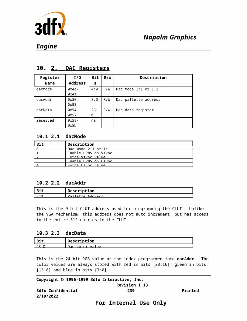
Napalm Graphics Engine (4x4). For FXT1 and DXT1, each compression block contains 32 texels (8x4). Each compression block can be referenced by the high-order bits of s & t, and the lod. Each of the 4 dwords in a block can be addressed using the dword select in bits [3:2] of the address.
The pci write would have to write to only the lower (s is even) two bytes of the address to insure that only texel 30, 45 is written.
Napalm will allow texture memory to be loaded from two different address spaces, the first being linear frame buffer space, and the second being the SST1 texture download port.
20.3 Maintaining cache coherency in NapalmNapalm has two TMUs, and thus two texture caches. Napalm needs explicit software intervention to maintain cache coherency.
The rules to maintain texture cache coherency with the frame buffer texture memory are as follows:
1. precede any group of texture downloads with a “pixel” flush of the 3d pipeline; ie. Issue a 2D NOPcmd to flush all pixels from the 3d section.
2. Next, perform texture downloads
3. Then, explicitly flush the texture cache, by changing the value of texBaseAddr. It is recommended that software write the inverse of the texBaseAddr to the register, and then re-write texBaseAddr with a correct value.
4. Now, again, do a “pixel” flush with a 2d NOPcmd. This will force all texture downloads to complete.
5. Now, procede with new rendering commands.
21. Programming Tips & Caveats The following is a list of programming guidelines which are detailed elsewhere but may have been overlooked or misunderstood:
21.1 Memory AccessesAll Memory accesses to Napalm registers must be 32-bit word accesses only. Linear frame buffer accesses may be 32-bit or 16-bit accesses, depending upon the linear frame buffer access format specified in lfbMode. Byte(8-bit) accesses are only allowed to Napalm linear frame buffer.
21.2 Determining Napalm Idle ConditionAfter certain Napalm operations, and specifically after linear frame buffer acceses, there exists a potential deadlock condition between internal Napalm state machines which is manifest when determining if the Napalm subsystem is idle. To avoid this problem, always issue a NOP command before reading the status register when polling on the Napalm busy bit. Also, to avoid asynchronous boundary conditions when determing the idle status, always read Napalm inactive in status three times. A sample code segment for determining Napalm idle status is as follows:
/********************************************************* * SST_IDLE: * returns 0 if SST is not idle * returns 1 if SST is idle *********************************************************/
Copyright 1996-1999 3dfx Interactive, Inc. Revision 1.133dfx Confidential 239 Printed 5/7/2023
For Internal Use Only

Napalm Graphics Engine SST_IDLE(){ ulong j, i; // Make sure SST state machines are idle PCI_MEM_WR(NOPCMD, 0x0); i = 0; while(1) { j = PCI_MEM_RD(STATUS); if(j & SST_BUSY) return(0); else i++; if(i > 3) return(1); }}
21.3 Triangle Subpixel CorrectionTriangle subpixel correction is performed in the on-chip triangle setup unit of Napalm. When subpixel correction is enabled (fbzColorPath(26)=1), the incoming starting color, depth, and texture coordinate parameters are all corrected for non-integer aligned starting triangle <x,y> coordinates. The subpixel correction in the triangle setup unit is performed as the starting color, depth, and texture coordinate parameters are read from the PCI FIFO. As a result, the exact data sent from the host CPU is changed to account for subpixel alignments. If a triangle is rendered with subpixel correction enabled, all subsequent triangles must resend starting color, depth, and texture coordinate parameters, otherwise the last triangle’s subpixel corrected starting parameters are subpixel corrected (again!), and incorrect results are generated.
21.4 32 BPP Rendering Enabling the destination alpha buffer. When 32 BPP rendering is enabled
(renderMode[1:0]=0x2), the destination alpha buffer is always automatically enabled, and fbzMode bit(18) (typically used to select the auxiliary buffer as a destination alpha buffer) must be cleared.
Write mask for the color buffers. When 32 BPP rendering is enabled, fbzMode bit(9) must be set to allow writes to any of the individual color planes, and renderMode bits (19:17) are used to control writes to each individual color plane. Note that clearing fbzMode bit(9) causes all color planes to not be written, regardless of the individual settings of renderMode bits(19:17).
Write mask for the depth and destination alpha buffers. When 32 BPP rendering is enabled, fbzMode bit(10) is used to enable writes to the depth buffer, and renderMode bit(20) is used to enable writes to the alpha buffer.
Write mask for the stencil buffer. When 32 BPP rendering is enabled, stencilMode bits(23:16) enables writes to the stencil buffer. During triangle rendering, individual bit write enable access is supported by setting corresponding bits in stencilMode bits(23:16). However, for the FASTFILL command, individual bit write enable control is not supported, and setting any bit in stencilMode bits(23:16) enables the 8-bit value of the stencil reference value (stencilMode bits(7:0)) to be stored in the stencil buffer.
Copyright 1996-1999 3dfx Interactive, Inc. Revision 1.133dfx Confidential 240 Printed 5/7/2023
For Internal Use Only
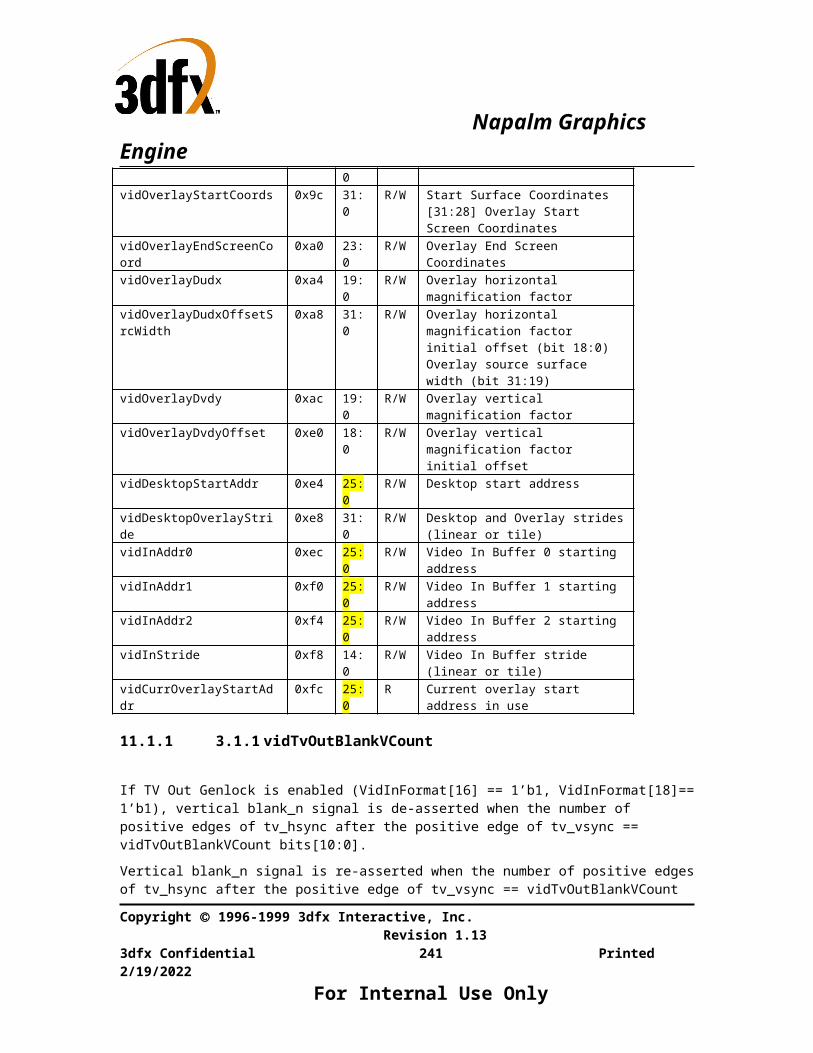
Napalm Graphics Engine 21.5 15 BPP Rendering Enabling the destination alpha buffer. When 15 BPP rendering is enabled
(renderMode[1:0]=0x1), the 1-bit destination alpha buffer is automatically enabled, and fbzMode bit(18) (typically used to select the auxiliary buffer as a destination alpha buffer) must be cleared.
Write mask for the destination alpha buffer. When 15 BPP rendering is enabled, there is no capability to disable writes to the destination alpha buffer separately from the color buffers. Writes to the destination alpha buffer are simultaneously enabled when writes to the RGB buffers are enabled (fbzMode bit(9)=1).
Clearing the destination alpha buffer. When 15 BPP rendering is enabled, there is no capability to selectively clear the 1-bit destination alpha buffer using the FASTFILL command. When using the FASTFILL command, both color and the 1-bit alpha information are written simultaneously. The only way to selectively clear the destination alpha buffer is to render a triangle and setup the alpha blending modes to not modify the RGB channels and only modify the alpha channel as desired. Also note that for the FASTFILL command, the value of the 1-bit alpha channel stored into the frame buffer is calculated as specified in the fastfillCMD register description.
21.6 2 Pixel-per-clock Rendering Enabling. 2 pixel-per-clock rendering is enabed by setting combineMode[29]. Note that 2 pixel-
per-clock rendering may only be enabled for single-textured triangles. It is required that software clear combineMode[29] when dual-texturing is desired.
Disabling. When changing state from 2 pixel-per-clock rendering to single pixel-per-clock rendering, 12 NOP commands must be send prior to the write which clears combineMode[29]. The 12 NOP commands should be directed using the chip field only at the TMUs, and not the FBI chip. See the combineMode register description for more information.
TMU State updates. When 2 pixel-per-clock rendering is enabled and miscInit1[18]=0, then any write to either TMU unit will be received by both (i.e. every write to a given TMU will be broadcast to both, regardless of the chip field value). This functionality can be disabled by setting miscInit1[18]=1.
TMU State. In 2 pixel-per-clock rendering, each texture unit is used to generate pixels in scanline “bands” (as controlled by renderMode[24:22]). As a result, it is required that each TMU’s state be identical (and each setup for single texture-per-pixel rendering operation) in order to have correct results. Software is required to ensure that each TMU state is identical and setup for single texturing operation.
Performance. 2 pixel-per-clock rendering will only increase performance when extra memory bandwidth is available. When extra memory bandwidth is not available, then 2 pixel-per-clock rendering should be disabled, as enabling 2 pixel-per-clock rendering may actually be slower than single pixel-per-clock rendering. As a result, 2 pixel-per-clock rendering should only be enabled for 15/16 bpp rendering modes, and should not be enabled for 32bpp rendering modes (except possibly for some very low resolutions). Also, for very high resolutions or high refresh rates, 2 pixel-per-clock rendering may need to be disabled even for 15/16 bpp rendering modes. This performance tweaking will need to be performed once actual silicon is available.
Performance Tweaking. When 2 pixel-per-clock rendering is enabled, the number of scanlines that are rendered by each texture unit is controlled by renderMode[24:22]. It is possible that different values may be required to tweak individual games or benchmarks. This performance tweaking will need to be performed once actual silicon is available.
21.7 Scanline Interleaving Y-origin swapping. Y-origin swapping must be used carefully when SLI is enabled. When Y-origin
swapping is enabled, the Y coordinate is subtracted from a constant to “flip” the origin from the upper-left to the lower-left corner of the screen. The problem this presents for SLI is that this
Copyright 1996-1999 3dfx Interactive, Inc. Revision 1.133dfx Confidential 241 Printed 5/7/2023
For Internal Use Only
Napalm Graphics Engine
“flipping” of the Y-coordinate causes scanlines which were not “owned” by a given chip to possibly be “owned” and visa-versa (because the Y-coordinate is changing). To address this issue, software must also “flip” the sli_comparemask fields in the sliCtrl register in order to compensate for the Y-coordinate “flipping.” Also, the constant value used to subtract the Y-coordinate from to accomplish this “flipping” will need to be divided by the number of chips in an SLI configuration due to the fact that the Y-address “munging” performed to pack a given chip’s memory occurs before the Y-coordinate “flipping.”
Access to a slave’s local memBaseAddr1 address space. When SLI and snooping are enabled, a slave’s local memBaseAddr1 address space is unavailable. Do not attempt to access via reads or writes a slave’s local memBaseAddr1 address space when SLI/snooping is enabled.
Performance Tweaking. When SLI is enabled, each chip “owns” a programmable number of scanline “bands.” The “band” height is set via the fields in the sliCtrl register. Performance tweaking will be required once silicon is available to program the optimal “band” height for performance. Note that different “band” heights may be required for different applications or benchmarks.
Dithering. Dithering does not work properly when the “band” height is 1. If dithering is desired, do not use a “band” height of 1.
PCI Wait States. When snooping is enabled, 2 PCI read wait states (pciInit0[8]=1) and 1 PCI write wait state (pciInit0[9]=1) must be used. Running with more aggressive wait state settings will break the snooping functionality.
FASTFILL command. The FASTFILL command has several problems when used in SLI configuration: (1) performance, and (2) compatibility when using SGRAM memories and filling tiled surfaces. See the fastfillCMD register description for more information. It is recommended that software use the 2D BLT engine to fill surfaces when in an SLI configuration.
21.8 Miscellaneous Control New texture and color combine operation. When the new texture and color combine unit
functionality of Napalm is required, combineMode[30] must be set to disable the use of the chromaKey and chromaRange for the texture color/chroma substitution function. Note that when the new texture and color combine unit functionality is enabled that the texture color/chroma substitution functionality is not available.
Guardband clipping coordinates. When guardband clipping is enabled (renderMode[21]=1), the left and right guardband clipping planes (as defined in clipLeftRight1) must be aligned to even pixels.
Performance tweaking using triangle iterators column band control. The triangle iterators’ column band control is specified in fbzColorPath[31:30]. This controls how many pixels to render horizontally before stepping down (to run in “legacy” performance mode set this field to 0x0 for 8-wide column rendering). Once silicon is available, performance tweaking will need to be performed to determine the optimal values for fbzColorpath[31:30]. Note that different values may need to be required for different applications and/or benchmarks.
PCI Read Wait States. 2 PCI read wait states should always be used (pciInit0[8]=1). A timing race condition exists when only a single PCI read wait state is used which may cause incorrect PCI read data being returned.
Frame Buffer Command FIFO. If the command FIFO is being maintained in frame buffer memory, it must be located in the lower 16 MBytes of memory. Placing the command FIFO in frame buffer memory above 16 MBytes is not supported.
Packet type 6. Packet type 6 is pretty much broken with AGP command fifos. Packet type 6 will work fine for frame buffer command fifos.
Dither rotation. The hardware has a bug which does not allow dither rotation to be used for FASTFILL commands or 3D LFBs. Dither rotation must be disabled by clearing renderMode[25] when performing FASTFILLs or 3D LFBs.
Copyright 1996-1999 3dfx Interactive, Inc. Revision 1.133dfx Confidential 242 Printed 5/7/2023
For Internal Use Only
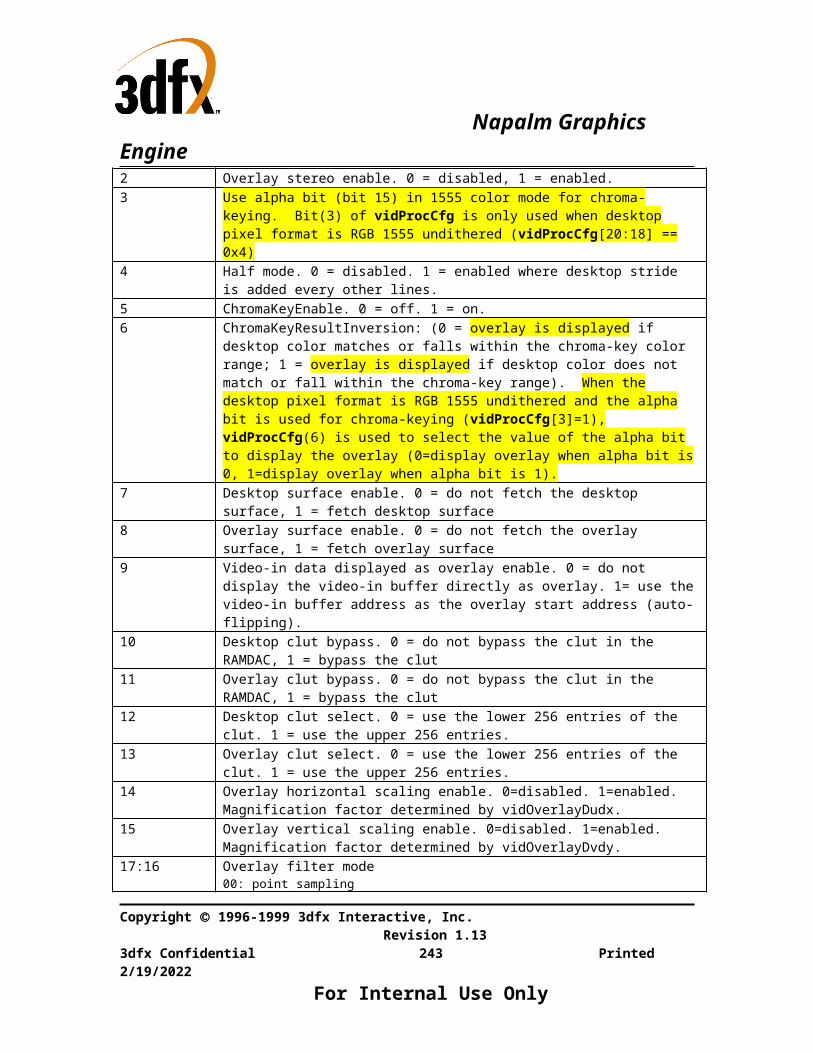
Napalm Graphics Engine 22. Accessing the ROM
22.1 ROM ConfigurationNapalm supports either 32K or 64K of ROM space. The size of the ROM is determined during at power up by an external strapping pin (see the section of strapping pins for more information).
Directly after reset, PCI subsystem and subvendor information are loaded from the next to last four bytes of ROM memory. The last four bytes are reserved for checksum information.
22.2 ROM ReadsNapalm supports reads to the ROM through the normal PCI mechanism. In order to read the ROM, set the romBaseAddr register bit 0 to 1. ROM accesses are then possible at the address indicated by the most significant bits of romBaseAddr. ROM reads can have any combination of byte enables asserted. Since the ROM is a byte device however, asserting multilble byte enables at once will cause the transfer of data on the PCI bus to be slow.
It is important to note the ROM shares the bus with VMI and TV out. During ROM accesses, data on these ports will become ROM information providing what may appear to be bad pixels on the display. This is normal; however, if it is know that ROM accesses are to occur, it is recommended that VMI or TV out be disabled prior to ROM access.
22.3 ROM WritesNapalm also supports a mechanism for programming flash ROMs when they are available. The model that Napalm uses is that of a 32K/64K EEPROM that allows programming by polling the EEPROM.
By default, Napalm will not respond to writes pointed at by romBaseAddr. By enabling bit 0 of romBaseAddr and also setting bit 4 of miscInit1, writes pointed at by romBaseAddr will be processed.
Typically, programmable ROMs have a sequence of write events that must occur to be placed in the ‘Program Mode’. Then either a single or multiple writes occur (depending of the ROM used) to fill in data. Finally, the ROM is polled via ROM reads, to confirm the write is complete. This process is repeated until the ROM is completely written.
For more information on how to program a specific ROM, see its data sheet or application notes.
23. Power on Strapping Pins During power up, Napalm gets some of its configuration information from strapping pins. This information is used to control how Napalm will behave. This power on strapping information is stored in 2 registers, strapInfo0 and strapInfo1 (both readable by reading from the strapInfo register), as defined below:
strapinfo0 RegisterBit Power On
Strapping PinDescription
31:24 n/a reserved23 TV_DATA_11 reserved22 TV_DATA_10 reserved21 TV_DATA_9 mctl_memory_port_config bit(2) (default tmuGbeInit[27])Copyright 1996-1999 3dfx Interactive, Inc. Revision 1.133dfx Confidential 243 Printed 5/7/2023
For Internal Use Only

Napalm Graphics Engine 20 TV_DATA_8 mctl_memory_port_config bit(1) (default tmuGbeInit[26])19 TV_DATA_7 mctl_memory_port_config bit(0) (default tmuGbeInit[25])18 TV_DATA_6 pci_device_id (0=device id is 6,7, 1=device id is 8,9)17 TV_DATA_5 pci_strapinfo1_zero (force strapInfo1 to 0x0)16 TV_DATA_4 mctl_dram_numbanks (default dramInit0[30])15 TV_DATA_3 SGRAM type bit(2) (default dramInit0[29])14 TV_DATA_2 SGRAM type bit(1) (default dramInit0[28])13 TV_DATA_1 AGP 4X Enable (0=Disabled, 1 = Enabled)12 TV_DATA_0 AGP 2X Enable (0=Disabled, 1 = Enabled)11 VMI_ADDR_3 PLL bypass (1=bypass)10 VMI_ADDR_2 mctl_type_sdram (default dramInit1[30])9 VMI_ADDR_1 mctl_short_power_on (0-normal power-on, 1=for RTL
simulation only)8 VMI_ADDR_0 re-map IDSEL (0=IDSEL is IDSEL, 1= PCI_AD_16 is
IDSEL)7 VMI_DATA_7 Disable PCI IRQ register (0=Enable, 1 = Disable).6 VMI_DATA_6 SGRAM type bit(0) (default dramInit0[27])5 VMI_DATA_5 SGRAM number of chips (default dramInit0[26])4 VMI_DATA_4 PCI Device Type (0= VGA, 1= Multimedia)3 VMI_DATA_3 AGP Enable (0=Disabled, 1 = Enabled).2 VMI_DATA_2 PCI 66Mhz (0 = 33Mhz, 1 =66Mhz)1 VMI_DATA_1 BIOS Size (0=32K, 1 = 64K)0 VMI_DATA_0 PCI Fast Device. (0=DEVSEL Medium,1= DEVSEL Fast)
When TV_DATA_5 is pulled high during power-up, the value of strapInfo1 will be forced to 0x0. Otherwise, the value of strapInfo1 is as defined below:
strapinfo1 RegisterBit Power On
Strapping PinDescription
31:24 n/a reserved23 FB_DATA_23 vga_valid_disable (default vgaInit0[3])22 FB_DATA_22 vga_legacy_addr_disable (default vgaInit0[9] and
vgaInit0[10])21 FB_DATA_21 vga_disable (default vgaInit0[1])20 FB_DATA_20 pci_multi_fctn_mmedia19 FB_DATA_19 pci_multi_fctn_device (default cfgInitEnable[28])18 FB_DATA_18 pci_disable_fctn_zero17 FB_DATA_17 pci_fctn_number bit(2)16 FB_DATA_16 pci_fctn_number bit(1)15 FB_DATA_15 pci_fctn_number bit(0)14 FB_DATA_14 chip ID bit(4)13 FB_DATA_13 chip ID bit(3)12 FB_DATA_12 chip ID bit(2)11 FB_DATA_11 chip ID bit(1)10 FB_DATA_10 chip ID bit(0)9 FB_DATA_9 pci_iobase_alloc bit(1)8 FB_DATA_8 pci_iobase_alloc bit(0)
Copyright 1996-1999 3dfx Interactive, Inc. Revision 1.133dfx Confidential 244 Printed 5/7/2023
For Internal Use Only
Napalm Graphics Engine 7 FB_DATA_7 pci_membase1_alloc bit(3)6 FB_DATA_6 pci_membase1_alloc bit(2)5 FB_DATA_5 pci_membase1_alloc bit(1)4 FB_DATA_4 pci_membase1_alloc bit(0)3 FB_DATA_3 pci_membase0_alloc bit(3)2 FB_DATA_2 pci_membase0_alloc bit(2)1 FB_DATA_1 pci_membase0_alloc bit(1)0 FB_DATA_0 pci_membase0_alloc bit(0)
strapInfo1 bits(3:0) and bits(7:4) determine the amount of address space that is requested by the device in the PCI configuration space for memBaseAddr0 and memBaseAddr1. By default, the amount of memory decoded is equal to the amount of memory requested, but this can be changed using the cfgPciDecode register. Bits(9:8) determine the amount of IO space that is requested by the device (0=256 bytes, 1=512 bytes, 2=1024 bytes, 3=2048 bytes). StrapInfo bits(14:8) define a unique chip ID used for multi-chip configurations. In multi-chip configurations, each chip must be assigned a unique ID value. Bits(17:15) define the PCI configuration space function number for the device, again used in multi-chip configurations. Bit(18) of strapInfo1 is used to disable responding to configuration space accesses to function zero. Bit(19) is used to specify that the device is a multi-function device in PCI configuration space. Bit(20) is used to report that a particular device is a multi-media class device when configured as a non-zero PCI configuration function number. Bit(21) is used to disable the VGA core, and bit(22) is used to disable the VGA legacy address space.
24. Signal Strapping The following signals need to be strapped on the Napalm board for proper functionality:
Signal Name Strappingpci_fifo_stall Pulldownpci_rdrdy Pulldownsli_syncin Pulldownsli_syncout Pulldownaa_valid Pulldownaa_clk Pulldownrom_cs_n Pulluprom_oe_n Pulluprom_we_n Pulluptest_enable Pulldowndac_hsync Pullup (for multi-chip only, where
dac_hsync gets driven by multiple chips and transition occurs in middle of active scanline)
vsync_ref Pulldownpd Pullup/Pulldown (pd upon poweron is
tristate. If using SiImage transmitter then must strap accordingly…)
Copyright 1996-1999 3dfx Interactive, Inc. Revision 1.133dfx Confidential 245 Printed 5/7/2023
For Internal Use Only
Napalm Graphics Engine 25. Monitor Sense Napalm Supports the ability to detect a monitor, as well as determine if the monitor is color or monochrome. This is accomplished with an internal MSENSE signal. MSENSE becomes active when a current is driven through either the RED, GREEN or BLUE DAC outputs. If a monochrome monitor is present, only the GREEN output will cause MSENSE to become active. MSENSE is readable through IO 0x3c2, bit 4.
26. Data Formats
Signal Pixel Sequence for 4 : 1 : 1 Pixel Sequence for 4 : 2 : 2
P15 Y7 Y7 Y7 Y7 Y7 Y7 Y7 Y7 Y7 Y7 Y7 Y7 Y7 Y7
P14 Y6 Y6 Y6 Y6 Y6 Y6 Y6 Y6 Y6 Y6 Y6 Y6 Y6 Y6
P13 Y5 Y5 Y5 Y5 Y5 Y5 Y5 Y5 Y5 Y5 Y5 Y5 Y5 Y5
P12 Y4 Y4 Y4 Y4 Y4 Y4 Y4 Y4 Y4 Y4 Y4 Y4 Y4 Y4
P11 Y3 Y3 Y3 Y3 Y3 Y3 Y3 Y3 Y3 Y3 Y3 Y3 Y3 Y3
P10 Y2 Y2 Y2 Y2 Y2 Y2 Y2 Y2 Y2 Y2 Y2 Y2 Y2 Y2
P9 Y1 Y1 Y1 Y1 Y1 Y1 Y1 Y1 Y1 Y1 Y1 Y1 Y1 Y1
P8 Y0 Y0 Y0 Y0 Y0 Y0 Y0 Y0 Y0 Y0 Y0 Y0 Y0 Y0
P7 U7 U5 U3 U1 U7 U5 U3 U1 U7 V7 U7 V7 U7 V7
P6 U6 U4 U2 U0 U6 U4 U2 U0 U6 V6 U6 V6 U6 V6
P5 V7 V5 V3 V1 V7 V5 V3 V1 U5 V5 U5 V5 U5 V5
P4 V6 V4 V2 V0 V6 V4 V2 V0 U4 V4 U4 V4 U4 V4
P3 0 0 0 0 0 0 0 0 U3 V3 U3 V3 U3 V3
P2 0 0 0 0 0 0 0 0 U2 V2 U2 V2 U2 V2
P1 0 0 0 0 0 0 0 0 U1 V1 U1 V1 U1 V1
P0 0 0 0 0 0 0 0 0 U0 V0 U0 V0 U0 V0
27. Issues/Requirements
27.1 PCI/AGP requirements Devsel needs to decoded for VGA Add 8bit xfers Add AGP bus master. Add interrupt logic Incorporate VGA information into PCI CFG space No wait state palette writes
Copyright 1996-1999 3dfx Interactive, Inc. Revision 1.133dfx Confidential 246 Printed 5/7/2023
For Internal Use Only

Napalm Graphics Engine 27.2 2D requirements (SST-G)
Binary / Ternary Rasterops 8x8x24 patterns Blits, src stride and dst stride. Stretch blits 1:n color expansion (text) lfb byte writes YUV - RGB color space conversion SGRAM fast fill Lines / Tri’s and rects use FBI fastfill / triangles. support 8bit, 16bit, and 24bit color formats
27.3 Video / Monitor requirements Anti Dither logic? Extra Gamma logic for 8bit desktop. 135 Mhz DAC (1280x1024 resolution) Triple 256x8 lookup tables Hardware Cursor
64x64x2 windows compatibleCursor image data stored in offscreen memorysingle 128 bit internal cache stores current scanline cursor informationCursor scanline is read during active hsyncregisters required curXpos, curYpos, curCtrl, CurC0, CurC1Cursor registers live in the pci domainX compatibility?
Window ID information for entire screen is RLE encoded and stored in offscreen memory Each window can be single or double buffered Each window can be YUV or 16 bit RGB format color Bilinear filtering in both X and Y support for window magnification Decimation (point sampling) for window minification Windows desktop is a special case (wid 0) and is single buffered, palettized or 16/24 RGB only 4 or 8 or 16 unique window Ids supported wid requires widRowStart(buffer0), widRowStart(buffer1), widRowStart(buffer2), widCtrl,
widXStartwidYStart, widXSize, widYSize, wid_dudx, wid_dvdy
Single 8 bit overlay with transparency? Pixel replication / line duplication for lower rez support (320x240) Software control of vsync/hsync DDC compliance vsync interrupts Genlock to external video source (tristate hsync/vsync controls) invert hsync/vsync LCD shutter glasses support Interlaced video output support Filtered interlaced video output support? Video in? S3 scenic Highway? VESA video In Port Support for VBE2.X LFB modes / and functions?
27.4 VGA Controller requirements Palette snooping Palette control in PCI space.
Copyright 1996-1999 3dfx Interactive, Inc. Revision 1.133dfx Confidential 247 Printed 5/7/2023
For Internal Use Only
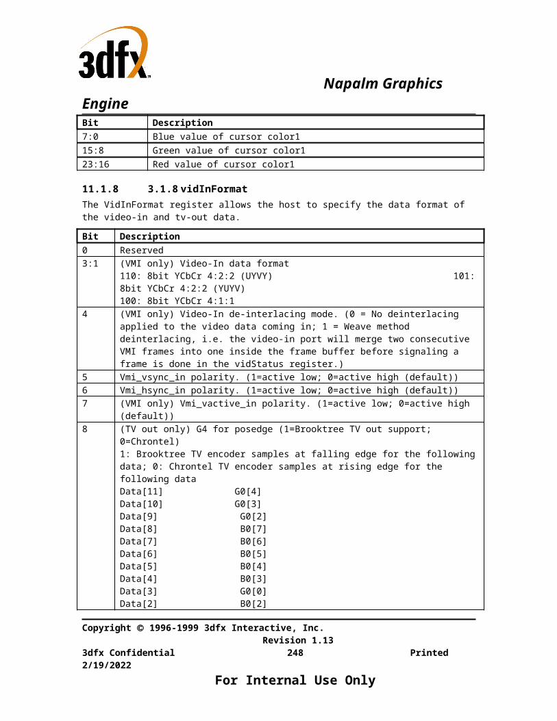
Napalm Graphics Engine
Relocatable VGA extension rom Needs to be disabled. Supports all VGA lfb modes including 4 bit planar.
27.5 Memory Controller requirements Combined Texture, 2D, 3D(color & auxillary), Video 128 bit wide Support SGRAM write per bit, block write. Continued support for EDO 3D in a window Bank / port swizzling for 2D and texture performance Texture cache. Arbitrate between VGA, 2D, FBI, TMU Packed 24 bit mode in addition to 8 bit and 16 bit pixel formats Tiled, interleaved bank memory organization for optimal performance.
27.6 Configuration Eeprom Serial Eeprom for storing video configuration Support for VGA rom expansion.
27.7 Dac requirements Must support pixel format switching per pixel Must support triple CLUT Must support >= 135Mhz pixel frequency. Must support 8 bit psuedo color lookup. Must reset to 8 bit psuedo color lookup VGA wants 18 bit clut writes. Support monitor sensing for VGA SAR at clut output for diagnostic/testability. Dac CLUT Addr (24bits) DAC CLUT data (18-24bits)
27.8 PLL requirements Must support video frequencies >= 135Mhz Graphics clock must reset >= 50Mhz < 75Mhz Video clock must reset = = 25.175 (VGA) PLL must support the following 2 frequencies in HW 25.175, and 28.322 Mhz for VGA Requires M / N register pair per PLL. M is 8 bits, N is 8 bits. (14.318Mhz source) PLL output test port.
27.9 Overall requirements Napalm must reset to VGA mode with no software help. Power down support? VBE 2.0 APM document?
27.10 PC97 requirements Primary graphics adapter does not use legacy bus Support for NTSC/PAL TV Support for multiple adapters / monitors Minimum resolution 1024x768x16 Graphics operations use relocatable registers only Graphics adapter operates normally with default VGA mode driver ( 4 bit planar )
Copyright 1996-1999 3dfx Interactive, Inc. Revision 1.133dfx Confidential 248 Printed 5/7/2023
For Internal Use Only
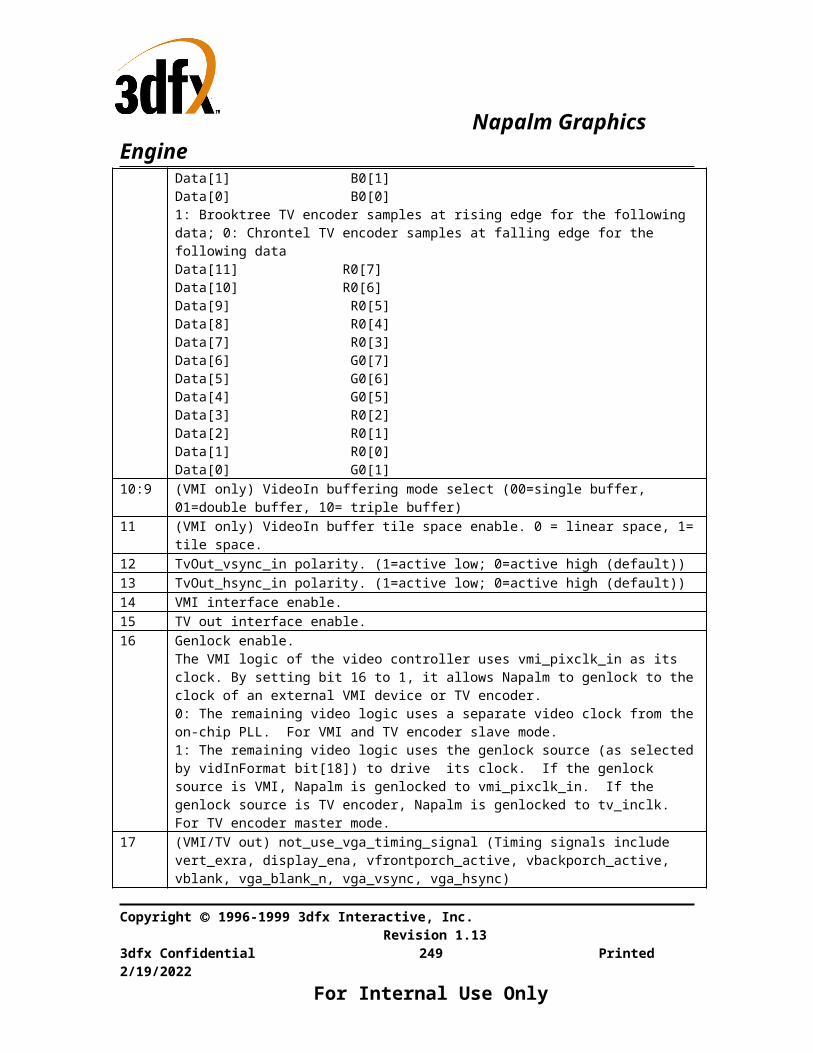
Napalm Graphics Engine
ergonomic timing rates per current VESA specification: 75Hz Color ordering rgb most significant is red least significant is blue, bpp 15, 16, 24, 32 Downloadable RAMDAC entries to support image color matching (gamma correction) Support of DDC 2.0 monitor detection VGA must be able to configure its bios base address to c000 Direct frame buffer access can be performed at any time If supported, low resolution modes are 320x200, 320x240, 400x300, 512x384, and 640x400 all
in 8 or 16 bit depths Hardware arithmetic stretching Transparent blter Perform double buffering with no tearing Current scan line of refresh Programmable blter stride (better memory management) YUV off-screen surfaces for color space conversion
27.11 Testability requirements Ram disable, Pll disable, blank for IDDQ. External access to pixel data at DAC input to verify DAC and pixel logic. Clock / PLL bypass for the tester. (2 pins, 1 for video, 1 for grx) Partial scan for coverage?
28. Revision History .10
YUV off-screen surfaces for color space conversion
.11
Split spec into multiple documents
(Following are for Napalm only)
1.00
General cleanup of text description of Napalm capabilities (e.g. mention 64 MByte support, true color rendering, AGP 4x, etc.)
Update “Hosts view of memory in VESA Modes” picture on last page of VGA spec Increased address width in 2D srcBaseAddr and dstBaseAddr to 26 bits to access 64 MBytes of
address space (bits 25:0 of each register now define base address) Fixed erroneous description of writing to sgram/sdram mode register using 2D engine. The
colorFore register is preloaded with the value desired to be written to the sgram/sdram mode register.
Added mapping of colorFore register to sgram/sdram pins in description of writing to the sgram/sdram mode register section (in 2D section)
Increased address width of 3D registers colBufferAddr and auxBufferAddr to 26 bits to access 64 MBytes of address space (bits 25:4 of each register now define the base address)
Increased width of 3D register leftOverlayBuff to 31. leftOverlayBuff[25:0] now define the 26-bit base address for 64 MBytes of address accessibility. leftOverlayBuff[31] defines whether the field is even or odd as required by the deinterlacing algorithm.
Increased address width of 3D register rightOverlayBuff to 26 bits to access 64 MBytes of address space (bits 25:0 now define the base address)
Copyright 1996-1999 3dfx Interactive, Inc. Revision 1.133dfx Confidential 249 Printed 5/7/2023
For Internal Use Only

Napalm Graphics Engine
Increase address width of 3D register texBaseAddr to 26 bits for 64 MByte address accessibility. 26-bit texture base address is now formed as {texBaseAddr[1], texBaseAddr[24:4], 0000}.
Increased width of 3D registers texBaseAddr1, texBaseAddr2, and texBaseAddr38 to 26-bits for 64 MByte address accessibility.
Increased width of video registers hwCurPatAddr, vidDesktopStartAddr, vidInAddr0, vidInAddr1, vidInAddr2, and vidCurrOverlayStartAddr to 26 bits for 64 MByte address accessibility.
Modified description of CMDFIFO packet types 5 and 6 to allow 27-bit address specification in word 1 for 128 MByte address accessibility (need 128 MByte address accessibility to be able to address lfb space in both tiled and linear, each being up to 64 Mbytes in size)
Increased width of agpGraphicsAddress register to 27 bits for 128 MByte address accessibility (need 128 MByte address accessibility to be able to address lfb space in both tiled and linear, each being up to 64 Mbytes in size)
Increased width of yuvBaseAddress register to 26 bits for 64 MByte address accessibility Changed default definition of PCI configuration registers memBaseAddr0 and
memBaseAddr1. Both memory base address registers now default to allocate 128 MBytes of memory space each from the system BIOS.
Added bits in lfbMemoryConfig register to be able to select between tiled and linear address space for 128 Mbytes of addressibility (tiled and linear address space, each up to 64 MBytes)
Added bits in dramInit0 to select 8, 16, 32, and 64 Mbit sgrams/sdrams, and also select between 2 and 4 internal bank sgrams/sdrams.
Added bits(24:23) in vgaInit0 to allow full 64 MByte addressibility for the starting page of VGA.
Added bits(30:29) in vgaInit1 to allow full 64 MByte addressibility for VBE write and read apertures.
Updated “Calculating texel addresses” section Added power on strapping pin definition for VMI_ADDR_3 (PLL bypass)
1.01
Added bit(3) of vidProcCfg register to control whether to use the alpha bit in the 1555 desktop mode for chroma-keying
Added new desktop pixel format RGB1555 undithered in vidProcCfg bits(20:18) Added new overlay pixel formats RGB1555 dithered, RGB1555 undithered, and RGB32
undithered in vidProcCfg bits(23:21) Changed dramInit1[12] to “reserved”. Dither pass-thru mode is no longer supported in order to
support 1555 ARGB and 8888 ARGB 3D rendering modes. Added renderMode register (32-bit) Added renderMode[1:0] to control 3D rendering mode (16BPP 565 RGB, 15BPP 1555 ARGB,
or 32BPP 8888 ARGB modes) Added renderMode[14:2] to allow dynamic setting of the Y-Origin subtraction value
1.02
Now zaColor[23:16] are used for upper byte for 24-bit depth data Added renderMode[16:15] to control the behavior of the 1-bit alpha channel when running in
15 BPP rendering mode Added section in “Programming Caveats” for 32 BPP and 15 BPP rendering. Added description of the alpha channel alpha blending modes for 15, 16, and 32 BPP rendering
modes in the alphaMode register description Added separate writes for R, G, B, and Alpha for 32 BPP rendering mode in renderMode[20:17] Added support for stenciling with the creation of the stencilMode and stencilOp registers
Copyright 1996-1999 3dfx Interactive, Inc. Revision 1.133dfx Confidential 250 Printed 5/7/2023
For Internal Use Only
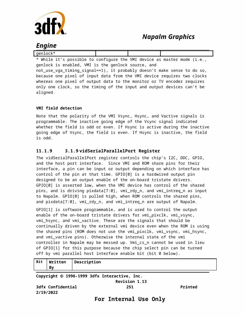
Napalm Graphics Engine
Added fbiStenciltestFail register Added linear write buffer write mode 0x8, which is a 24-bit depth value Added explanation under lfbMode register of how linear frame buffer writes work when running
in 32BPP rendering mode Documented in the zaColor register description the different use of zaColor depending on
whether 32BPP rendering mode is selected
1.03
Adding additional power-on strapping pins Added section of additional pins for Napalm (as compared to Avenger)
1.04
Added further description of using the FASTFILL command when running in 32 BPP rendering mode under the fastfillCMD register description and in the “Command Descriptions” section
Clarifications to 32-bit depth linear frame buffer write format (format 8) in lfbMode register description
Added description of the stencil write mask capabilities in the “Programming Caveats” section Added new alpha blending functions A_SAMECOLOR and AOM_SAMECOLOR to allow
src*src and dst*dst blending calculations
1.05
Changed ordering of stencil operations in the stencilOp register to match D3D spec Added poweron strapping values for dramInit0[29:28] Changed alpha-channel alpha blending factors for 15 BPP rendering mode to only be 0 and 1
(just like 16 BPP rendering mode) Added combineMode register Updated CCU and ACU block diagrams under the fbzColorPath register description Added description in chromaRange and chromaKey for specifying constant colors into the
texture units Clarified behavior of linear frame buffer writes which bypass the pixel pipeline when running in
15 BPP rendering mode which do not contain alpha information in the lfbMode register desciption
Added SLI support in renderMode[31:29], commandExtra[31:29], and added new PCI config register cfgSliCtrl[31:0]
1.06
Updated CCU, ACU, Texture CCU, and Texture ACU diagrams
1.07 Clarified FASTFILL operation when running in 15 BPP rendering mode and where the single bit
alpha value comes from. Clarified description of cc_outshift and cca_outshift in combineMode Added reversal of operations and subtraction capabilities for alpha blenders in the fogMode and
alphaMode register descriptions
1.08 Added miscinit1[18] to disable broadcasting of TMU writes to both TMUs when 2 pixel-per-
clock mode is enabled Cleaned up naming conventions of clipping registers
Copyright 1996-1999 3dfx Interactive, Inc. Revision 1.133dfx Confidential 251 Printed 5/7/2023
For Internal Use Only
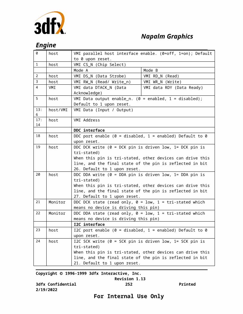
Napalm Graphics Engine
Added renderMode[21] to control triangle iterators guardband clipping, and added description of how to use guardband clipping in the clipTopBottom1 register description
Added 2 pixel-per-clock operation in combineMode and renderMode registers Added triangle column band selection in fbzColorPath[31:30] Added sliCtrl register Added aaCtrl register and description of Secondary rendering buffers in colBufferAddr and
auxBufferAddr register descriptions Added chipMask register Added chipID field in power on strapping values and in cfgSliCtrl[31:28] Cleaned up status register bit descriptions
1.09 Removed renderMode[31:29] (old SLI support) Moved mctl_dram_numbanks field in dramInit0 to dramInit0[30], with default value controlled
by reset value of TV_DATA_4 Added 1 bit to sgram type field in dramInit0[29:27] with default value controlled by reset value
of {TV_DATA_3, TV_DATA_2, VMI_DATA_6} Removed byte swizzling and word swapping of 2D, 3D, and non-modal LFB space as defined in
miscInit0[3:2] and miscInit0[31:30] Added address-based byte swizzling and word swapping for memBaseAddr1 as controlled by
miscInit1[22:20] Added strapInfo1 and lots of new poweron strapping values Added some placeholders in the “Programming Caveats” section Added the new 4 Meg TMU0 texture download aperture to the memory map (Section 7). Added texture format 15 (8888 ARGB) to the description of tformat (Section 11.72). Modified the texture download description (Section 23). Expanded the TMU0 texture download aperture in the memory map to 64 Meg (Section 7). Added the tbig bit to the tLOD register. (Section 11.73). Modified the texture download description (Section 23). Modified the packet 5 description (Section 12.1.8). Added the tcompressed bit to the textureMode register. (Section 11.73). Modified the texture download description (Section 23).
1.10 Added configuration registers cfgPciDecode, cfgVideoCtrl0, cfgVideoCtrl1, cfgVideoCtrl2,
cfgSliLfbCtrl, cfgSliAaTiledAperture, and cfgAaLfbCtrl Added configuration registers agpTestCtrl, agpTestData0, agpTestData1, agpTestData2, and
agpTestData3 Moved around poweron strapping bits Updated description of memBaseAddr0 and memBaseAddr1 VBE write aperture bits(11:10) now in vgaInit1[30:29] VBE read aperture bits(11:10) now in vgaInit0[26:25] Changed poweron value of vgaInit0[0] to be poweron strap value FB_DATA_21, and poweron
value of vgaInit0[9:8] to be poweron strap value {FB_DATA_22, FB_DATA_22}. Added vga_valid_disable in vgaInit0[3] with default poweron strap value FB_DATA_23.
Added note in pciInit0 that wait state bits (9:8) must both be set when bus snooping is enabled Added dither rotate functionality in renderMode[25] and fogMode[19:12] Added more bits in cmdFifoThresh Misc. changes to cfgInitEnable Added leftDesktopBuf register Added swapbufferCMD bit(10) to enable desktop swaps
Copyright 1996-1999 3dfx Interactive, Inc. Revision 1.133dfx Confidential 252 Printed 5/7/2023
For Internal Use Only

Napalm Graphics Engine
Added vidCurrDesktopStartAddr, read by writing bit(31) of IO address 0xfc and then reading IO address 0xfc
Added aaCtrl[30] to disable triangles to the primary rendering buffers when anti-aliasing is enabled
Cleaned up some out-of-date info in the register bit field descriptions of fbzColorPath and textureMode
Updated “Programming Tips & Caveats” section Renamed Avenger+ to Napalm
1.11 Added Signal Strapping section Added bits(24:20) in tmuGbeInit to control clock delay settings for aa_clk signal cfgVideoCtrl0 bits(23:20) are now reserved (old aa_clk_del_adj[3:0] field) Added cfgSliAaMisc register Added aa_lfb_rd_format field to cfgAaLfbCtrl miscInit1[31:29] now control pd pin Added pci_device_id for poweron value of TV_DATA_6 Changed lfbMemoryConfig to now consist of lfbMemoryTileCtrl and
lfbMemoryTileCompare Renamed cfgSliAaTiledAperture to cfgAaDepthBufferAperture and added window
comparison for the depth buffer for AA reads Added miscInit0[31] to enable queued VMI host port writes Added lfbMode write format 9 for queued VMI host port writes Added miscInit0[30] to control access to the vip2vmiCtrl register Added vip2vmiCtrl register description Updated deviceID register to reflect ability to choose ID values of {6,7,8,9} Fixed textual description of stencilOp register Added problems with command fifo packet type 6 when using an AGP command fifo to the
“Programming Caveats” section
1.12 Added description of vip2vmi_intr_field and vip2vmi_intr_type in vip2vmiCtrl register Fixed width of agpGraphicsStride in the AGP/CMD register map Clarified agpReqSize register description Fixed typo in chipMask register description. 32 chips are supported. Fixed typo in clipLeftRight1/ClipTopBottom1 register description Changed default value of Revision_ID register to be 0x1 Fixed “lfb” (should be “lsb”) typo in the Device_ID register description Added note in CMDFIFO Packet Type 6 which states that Packet Type 6 may only be used with
frame buffer command FIFOs Updated CMDFIFO Packet Types 1 and 4 with proper chip field bits Added clarification in description of chipMask register that the chipMask register can only
disable writes to the 3D registers and 3D LFB space Fixed typo in aaCtrl register description -- secondary buffer offsets are controlled by aaCtrl
bits(27:14) Added hotplug interrupts in intrCtrl register
1.13 Updated Programming Tips and combineMode register description to document workaround
required when switching from 2 pixel-per-clock rendering mode to single pixel-per-clock rendering mode
Copyright 1996-1999 3dfx Interactive, Inc. Revision 1.133dfx Confidential 253 Printed 5/7/2023
For Internal Use Only

Napalm Graphics Engine
Documented dither rotation capabilities in the renderMode register description. Updated fogMode register to clarify dither rotation capabilities.
Document bug with dither rotation when using FASTFILL commands and 3D LFBs in the Programming Tips section and the renderMode register description
Fixed 3D register description table so that nopCMD, combineMode, sliCtrl, and aaCtrl are now properly labeled as maskable registers
Added note about bugs in the FASTFILL command when in SLI Added aaCtrl bit(31) to enable auto reset of the cmd_repeat fifo (must be set if the triangle
setup unit is performing backface culling…) Updated 2D commandExtra register bits(31:28). Formerly used for SLI functionality. SLI is
not supported in the silicon, so these bits are now reserved Updated 3D chipMask register to remove references to cfgSliCtrl register Changes for Napalm2 (features not present in original Napalm):
Added tmuGbeInit[27:25] for mctl_memory_port_config Added dramInit0[31] for bit(1) of tWL Added dramInit1[31] for bit(1) of tRL Updated DEVICE_ID pci configuration register
Copyright 1996-1999 3dfx Interactive, Inc. Revision 1.133dfx Confidential 254 Printed 5/7/2023
For Internal Use Only