Oil & Natural Gas Technology - National Energy … library/Research/oil-gas/NT42948... · Oil &...
53
Oil & Natural Gas Technology 275° C DOWNHOLE SWITCHED-MODE POWER SUPPLY Final Report TECHNICAL PROGRESS REPORT For Period 9/20/06 to 8/31/08 by Chris Hutchens, Principal Investigator/Program Manager, & Vijay Madhuravasal, Investigator MSVLSI Group ATRC CEAT-ECEN Oklahoma State University. Stillwater, OK 74078 DOE Award No.: DE-FC26-06NT42948 Prepared for: United States Department of Energy National Energy Technology Laboratory Office of Fossil Energy
Transcript of Oil & Natural Gas Technology - National Energy … library/Research/oil-gas/NT42948... · Oil &...
Oil & Natural Gas Technology
275° C DOWNHOLE SWITCHED-MODE
POWER SUPPLY
Final Report
TECHNICAL PROGRESS REPORT
For Period
9/20/06 to 8/31/08 by
Chris Hutchens, Principal Investigator/Program Manager, &
Vijay Madhuravasal, Investigator MSVLSI Group ATRC
CEAT-ECEN Oklahoma State University.
Stillwater, OK 74078
DOE Award No.: DE-FC26-06NT42948
Prepared for: United States Department of Energy
National Energy Technology Laboratory
Office of Fossil Energy
Table of Contents List of Figures ..................................................................................................................... 4 Nomenclature ...................................................................................................................... 5 Abstract ............................................................................................................................... 7 Executive Summary ............................................................................................................ 8 1.0 Introduction ............................................................................................................. 9 2.0 Progress on scheduled tasks .................................................................................... 9
Task 1 through 3 ........................................................................................................... 10 Task 4 ............................................................................................................................ 10
Subtask 4.1.1 ............................................................................................................. 10 Subtask 4.1.2 ............................................................................................................. 10 Subtask 4.1.3 ............................................................................................................. 11 Subtask 4.1.4 ............................................................................................................. 11 --MILESTONE 1a: ................................................................................................... 11 Subtask 4.1.5 ............................................................................................................. 11 Subtask 4.1.6 ............................................................................................................. 11 Subtask 4.2.1 ............................................................................................................. 12 Subtask 4.2.2 ............................................................................................................. 15 Subtask 4.2.3 ............................................................................................................. 18
Task 5 ............................................................................................................................ 20 Subtask 5.1 ................................................................................................................ 20 Subtask 5.2 ................................................................................................................ 22
Packaging solution ................................................................................................ 24 Task 6.0 ......................................................................................................................... 25
Subtask 6.1 ................................................................................................................ 25 Subtask 6.1 ................................................................................................................ 27 Subtask 6.2 ................................................................................................................ 27
Task 7 ............................................................................................................................ 27 Subtask 7.1 ................................................................................................................ 28 Subtask 7.1.1 ............................................................................................................. 28
Voltage Reference: ................................................................................................ 29 Error Amplifier ..................................................................................................... 31 Dual Comparator ................................................................................................... 33 Hysteretic Comparator .......................................................................................... 35
Subtask 7.1.2 ............................................................................................................. 37 Subtask 7.1.3 ............................................................................................................. 37 Subtask 7.1.4 ............................................................................................................. 37 Subtask 7.1.5 ............................................................................................................. 37 --MILESTONE 2a: ................................................................................................... 37
3.0 SMPS testing results ............................................................................................. 38 Circuit board assembly ......................................................................................... 38 Test setup .............................................................................................................. 39 Test results ............................................................................................................ 39 3.3V converter....................................................................................................... 40 Control loop stability ............................................................................................ 42
2
3
The 5V module ..................................................................................................... 43 Performance summary .......................................................................................... 44 Limitations ............................................................................................................ 44 Conclusions ........................................................................................................... 45 Miscellaneous ....................................................................................................... 46 Technology transfer .............................................................................................. 46 Technical notes and future plans ........................................................................... 46
4.0 Appendix A – Analog blocks datasheets .............................................................. 47 Voltage Reference ................................................................................................. 47 Error amplifier ...................................................................................................... 48 Dual comparator.................................................................................................... 49 Hysteretic comparator ........................................................................................... 50
5.0 Appendix B ........................................................................................................... 51 Transfer function of the buck converter loop ....................................................... 51 V2 control IC Data sheet....................................................................................... 52
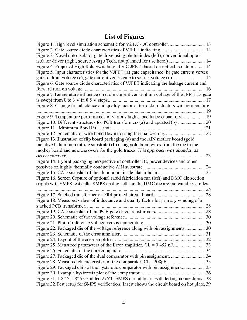
List of Figures Figure 1. High level simulation schematic for V2 DC-DC controller. ............................. 13 Figure 2. Gate source diode characteristics of VJFET indicating .................................... 14 Figure 3. Novel opto-isolator gate drive using photodiodes (left), conventional opto-isolator driver (right, source Avago Tech. not planned for use here.) .............................. 14 Figure 4. Proposed High-Side Switching of SiC JFETs based on optical isolation. ........ 14 Figure 5. Input characteristics for the VJFET (a) gate capacitance (b) gate current verses gate to drain voltage (c), gate current verses gate to source voltage (d) ........................... 15 Figure 6. Gate source diode characteristics of VJFET indicating the leakage current and forward turn on voltage. .................................................................................................... 16 Figure 7.Temperature influence on drain current versus drain voltage of the JFETs as gate is swept from 0 to 3 V in 0.5 V steps ................................................................................ 17 Figure 8. Change in inductance and quality factor of torroidal inductors with temperature........................................................................................................................................... 19 Figure 9. Temperature performance of various high capacitance capacitors. .................. 19 Figure 10. Different structures for PCB transformers (a) and updated (b). ...................... 20 Figure 11. Minimum Bond Pull Limit. ............................................................................ 21 Figure 12. Schematic of wire bond flexure during thermal cycling. ................................ 22 Figure 13.Illustration of flip board packaging (a) and the AlN mother board (gold metalized aluminum nitride substrate) (b) using gold bond wires from the die to the mother board and as cross overs for the gold traces. This approach was abandon as overly complex. ................................................................................................................. 23 Figure 14. Hybrid packaging perspective of controller IC, power devices and other passives on highly thermally conductive AlN substrate. .................................................. 24 Figure 15. CAD snapshot of the aluminum nitride planar board. ..................................... 25 Figure 16. Screen Capture of optional rapid fabrication run (left) and DMC die section (right) with SMPS test cells. SMPS analog cells on the DMC die are indicated by circles............................................................................................................................................ 25 Figure 17. Stacked transformer on FR4 printed circuit board. ......................................... 28 Figure 18. Measured values of inductance and quality factor for primary winding of a stacked PCB transformer. ................................................................................................. 28 Figure 19. CAD snapshot of the PCB gate drive transformers. ........................................ 28 Figure 20. Schematic of the voltage reference. ................................................................. 30 Figure 21. Plot of reference voltage versus temperature. ................................................. 30 Figure 22. Packaged die of the voltage reference along with pin assignments. ............... 30 Figure 23. Schematic of the error amplifier. ..................................................................... 31 Figure 24. Layout of the error amplifier. .......................................................................... 32 Figure 25. Measured parameters of the Error amplifier, CL = 0.452 nF. ......................... 33 Figure 26. Schematic of the core comparator. .................................................................. 34 Figure 27. Packaged die of the dual comparator with pin assignment. ............................ 34 Figure 28. Measured characteristics of the comparator, CL =208pF. .............................. 35 Figure 29. Packaged chip of the hysteretic comparator with pin assignment ................... 35 Figure 30. Example hysteresis plot of the comparator. .................................................... 36 Figure 31. 1.8” × 1.8”Assembled 275°C SMPS circuit board with testing connections. . 38 Figure 32.Test setup for SMPS verification. Insert shows the circuit board on hot plate. 39
4

Figure 33. Schematic of the under voltage lockout circuitry ............................................ 40 Figure 34. Performance of UVLO at normal and elevated tempearature ......................... 40 Figure 35. Transient output voltage plot of the 3.3V converter showing a 3 V overshoot at start up and the steady-state value .................................................................................... 40 Figure 36. Transient output voltage plot of the 3.3V converter showing the overshoot and state-state value with 47 ohms .......................................................................................... 40 Figure 37.Transient output voltage plot of the 3.3 V converter. ....................................... 41 Figure 38. Startup characteristic of the 3V converter with 47 ohm resistive load - 275°C............................................................................................................................................ 41 Figure 39. Startup characteristic of the 3V converter with 8.2 ohm resistive load - 275°C............................................................................................................................................ 41 Figure 40. Simplified control loop with equivalent circuit (a) and output transient response to a 12.5% output referred change by pulsing the 400mV voltage reference with a 350 to 450 mV pulse train. ............................................................................................. 42 Figure 41. Transient output voltage plot of the 5 V converter showing a 2 V overshoot at start up an the steady-state value under no load conditions. ............................................ 43 Figure 42. Transient output voltage plot of the 5 V converter showing a 2 V overshoot at start up and the steady-state value under a load of 47 ohms. ........................................... 43 Figure 43. Control loop behavior for step +/- 100 mV step change applied at the reference input of the 5V SMPS module under no load conditions. ................................................ 43 Figure 44. Modified board with self assembled gate drive transformer. .......................... 44 Figure 45. Expected frequency response of the buck converter loop transfer function. .. 51 Figure 46. Dice snapshot and pad out details of V2 control IC. ....................................... 52
Nomenclature AlN Aluminum Nitride CAD Computer Aided Design CISS Input capacitance of a power FET transistor CMOS Complementary Metal Oxide Semiconductor CMR Common Mode Range CTAT Complementary To Absolute Temperature ESR Equivalent Series Resistance GBP Gain Bandwidth Product IC Integrated Circuit JFET Junction Field Effect Transistor LVS Layout versus Schematic MHz Mega Hertz MOS Metal Oxide Semiconductor MPP Molybdenum Permalloy Powder MWD Measuring While Drilling NMOS N-type Metal Oxide Semiconductor OpAmp Operation Amplifier OTA Operational Transconductance Amplifier PCB Printed Circuit Board
5

6
PFM Pulse Frequency Modulation PMOS P-type Metal Oxide Semiconductor PTAT Proportional To Absolute Temperature PWM Pulse Width Modulation SiC Silicon Carbide SMPS Switched Mode Power Supply SOS Silicon on Sapphire S-parameter Scattering Parameters SPICE Simulation Program for Integrated Circuit Emphasis UV Ultra Violet UVLO Under Voltage Lock Out V2 Vee square control VDS Drain to source voltage VJFET Vertical Junction Field Effect Transistor VREF Voltage Reference Units and symbols f Femto 1×10-15
p Pico 1×10-12 n Nano 1×10⁻⁹ µ micro 1×10⁻⁶
m milli 1×10⁻³
F Farad H Henry A Ampere S Seconds V Volts Hz Hertz db Decibel Verilog-A: hardware description language specifically for analog components
Abstract A vee-square (V2) control based controller IC is developed for a switch mode power supply capable of operating at extreme temperature / harsh environment conditions. A buck type regulator with silicon carbide power junction field effect transistors (JFET) as power devices is used to analyze the performance of controller. Special emphases are made on the analog sub-blocks - voltage reference, operational transconductance amplifier and comparator as individual building blocks. Transformer coupled gate drives and high temperature operable magnetic cores and capacitors are identified and tested for use in the design. Conventional ceramic chip packaging of ICs combined with lead carrier type mounting of passive filter components is introduced for hybrid packaging of the complete product. The developed SMPS is anticipated to support the operation of down-hole microcontrollers and other electronics devices that require low/medium power filtered dc inputs over an operating temperature of 275° C. Keywords: dc-dc converter, vee-square, buck, smps, SOS, soi, silicon carbide, high temperature, gate drive. "This report was prepared as an account of work sponsored by an agency of the United States Government. Neither the United States Government nor any agency thereof, nor any of their employees, makes any warranty, express or implied, or assumes any legal liability or responsibility for the accuracy, completeness, or usefulness of any information, apparatus, product, or process disclosed, or represents that its use would not infringe privately owned rights. Reference herein to any specific commercial product, process, or service by trade name, trademark, manufacturer, or otherwise does not necessarily constitute or imply its endorsement, recommendation, or favoring by the United States Government or any agency thereof. The views and opinions of authors expressed herein do not necessarily state or reflect those of the United States Government or any agency thereof."
7
Executive Summary For the first time a room to 275°C switched mode power supply controller integrated circuit has been designed, fabricated, and demonstrated (anecdotal evidence suggest temperatures lower than -50°C are feasible with the present design.) The final buck controller integrated circuit (IC) die is less than 4mm2 and with a final cleanup area should be less than 3mm2 requiring only 5 discrete components to develop a 275°C power supply. The discretes consist of two SiC FET switches, the buck L-C and a small compensation capacitor. A 275°C 5 watt power supply was demonstrated within this task. Greater increments in power are possible incrementally by; 1) changing the voltage level or adding load capacitance, 2) by changing the power switches and increasing the load capacitor, and 3) replacing all components, all with no change to the existing controller IC. This effort contains many firsts; the first 275°C vee-square (V2) switched mode control IC, first voltage reference IC, first dual comparator IC, first hysteretic comparator IC, all operational beyond 275°C. See Appendix A – Analog blocks datasheets. The first use of SiC “enhancement” mode JFETs in a 275°C application and finally the first fully integrated high side switch circuit for -50 to 275°C operation. All analog cells were developed to implement a 5 watt switch mode power supply demonstration for extreme temperature / harsh environment conditions to 275°C for 1.5 to 28V. Special efforts were made to convert/condition and pad out the analog sub-blocks - voltage reference, operational transconductance amplifier, “NE555”, and comparators. All for use as individual building blocks in future applications. Transformer coupled gate drives and high temperature operable magnetic cores and capacitors suitable for high temperature were identified and tested for use in the design and used in this demonstration. Evaluation of these efforts pointed out two areas in great need of attention for successful 275°C electronics; reliable inexpensive (in relative terms) packaging and high valued i.e. µF, high temperature capacitors. No existing commercial printed circuit boards are suitable for above approximately 240° C applications. SOS CMOS, SiC enhancement JFETs, core inductors and low valued ceramic capacitors proved to be valuable and well suited for the operational temperature range from -50 to 275° C. A quasi “conventional” ceramic chip packaging of ICs combined with lead carrier type mounting of passive filter components was introduced for hybrid packaging of the complete product. The packaging consisted of an AlN gold motherboard to provide through hole mounting of large components i.e. inductor and input output signals and surface mount area over which a AlN window was AuGe soldered and gold package lead soldered. See Figure 14. The packaging effort proved to be fragile as a result of making the AlN motherboard too thin. The developed SMPS demonstration power supply was demonstrated functional for both 3 and 5 volts at 5 Watt and at room and 275° C. Table 5 presents a summary of the SMPS performance, target specifications and related comments. In the AlN board version overshoot was observed during startup at room temperature (See Figures Figure 35 and Figure 36.) suggesting that either the soft start circuit is ramping up too fast or the load capacitor ESR is lower than expected resulting poor compensation.
8
1.0 Introduction Among the more critical electronic systems needs for extreme temperature subsurface operations, are a high efficiency DC power supply. The key requirements of high efficiency and small size necessitate that it be a switched-mode power supply (SMPS). Such power supplies typically use high frequency switching at frequencies of 50 kHz to 1 MHz to periodically sample and store energy in an inductor, and then convert stored as magnetic energy to charge on a filter capacitor to the desired voltage. Regulation of a SMPS is performed using a feedback control loop to vary the duty cycle of the switch, which regulates the supply output voltage. Moreover, selecting a higher switching frequency greatly reduces the size of inductors and filter capacitors in the circuit, and allows attainment of power conversion efficiencies up to 95% for high performance multiple output voltage designs. Typical power efficiencies for most SMPS applications are 75 to 90%. The objective of this project is to produce a downhole switched-mode power supply (SMPS) capable of operating at 275°C for 1,000 hours, tailored to well logging and MWD applications. However, the resulting solution can be easily modified to satisfy the needs of emerging high temperature electronic systems for the aerospace industry. The base components of SMPS are a V2 controller, Buck Converter, and SiC power switches. These components will be placed in a package capable of operation at 275°C for 1,000 hours.
2.0 Progress on scheduled tasks The total project duration is 18 months and the work breakdown is outlined below. The project is to be executed in eight tasks: Task 1.0 Research Management Plan Task 2.0 Technology Status Assessment Task 3.0 Formation of an Industry Advisory Committee Task 4.0 V2 DC-DC power supply design Task 5.0 Packaging design Task 6.0 Optional rapid fabrication Task 7.0 Integration and packaging of the power supply Task 8.0 Write Commercialization Plan The first six tasks will overlap in time during the first year while the seventh task, beginning in the first year of the project, extends through the second year of the project. On December 31, 2006, we completed the first quarter of work on the project. All tasks are 100% complete as rescheduled and as budgeted with the exception of Task 8. Task 3 established an Industry Advisory Committee to aid in guiding the general direction of this project to provide a suitable switched-mode power supply for energy
9
industry. The advisory committee made a single request regarding functionality of the SMPS, not specified in the proposal. That an over temperature shut down feature be added to protect the SMPS controller. This has been successfully integrated into the SMPS IC.
The first six tasks will overlap in time during the first year while the seventh task, beginning in the first year of the project, extends through the second year of the project. On December 31, 2006, we completed the first quarter of work on the project. Task 1 through 3 - Task 1, Task 2, and Task 3 were 100% completed as scheduled under the original schedule and as budgeted at an expenditure of $10,972. Task 1 was to develop the Research Management Plan. The plan was developed interactively via email with the DOE contract monitor. Task 2, Technology Status Assessment result in a white paper on the current state of the art of high temperature power supply controller as of October, 2006. Task 3 established an Industry Advisory Committee to aid in guiding the general direction of this project to provide a suitable switched-mode power supply for energy industry. Teh advisory committee made a request that an over temperature shut down protection feature be added to protect the SMPS controller. See Hysteretic Comparator and Voltage Reference sections. Task 4 - V2 DC-DC power supply design includes the buck converter circuit, SOS-based V2 controller IC, SiC switches, and its associated extreme temperature packaging. This task consists of two main subtasks: Subtask 4.1 design of the V2 DC-DC controller IC and subtask 4.2 design of the Buck Converter. Subtask 4.1 is 100% complete. Subtask 4.1.1 - V2 DC-DC controller IC design was planned for a duration of 11 weeks, 10/2/06 to 12/15/06. The responsible teams include the Analog cell design and System timing integration teams. This task is 100% complete. This subtask involved design of 5 mixed signal cells: 1) Comparator without hysteresis, 2) Comparator with hysteresis, 3) Operational Transconductor Amplifier or OTA (An OTA is an unbuffered amplifier) 4) Voltage reference, and 5) Digital logic including ancillary protection circuits. These designs are the basic mixed signal building blocks that will be used in the final controller IC and were placed on the second downhole microcomputer-HC11 full wafer run. These designs under went a critical design review in the next month. The result of this review were a rework any cells which might be in question and as necessary delayed and placed the earliest possible Peregrine engineering run, either February or March 15th, 2007. This task is 100% complete. Subtask 4.1.2 - Pre-submission review was planned for duration 2 weeks, 12/18/06 to 12/29/06 and is 100% complete. An extensive in-house review was conducted to insure the elimination of errors prior to submission for fabrication. In Subtask 4.1.3 the
10

submitted mixed signal cells were revised as needed. This task is 100% complete. In Subtask 4.1.4 the mixed signal building bock cells were submitted for fabrication 3 weeks ahead of schedule. This was at no cost to the project as all cells placed on the OSU HC11 run which covered the cost. These funds were later used for an additional unscheduled fabrication run. Subtask 4.1.3 – Revised mixed signal cells as required Duration of Task: 2 weeks, 1/1/07 to 1/12/07 Responsible Team: Analog cell design 100% Complete. Subtask 4.1.4 – Mixed signal cells fabrication submission Duration of Task: 13 weeks, 1/15/07 to 4/13/07 Responsible Team: Mixed signal control The layouts of the mixed signal cells from in Subtasks 4.1.1 to 4.3.3 were submitted to Peregrine’s foundry for fabrication as an “engineering run”. Engineering runs differ from a full fabrication by being smaller in area and lower in cost. This requires 13 weeks from submission to delivery of wafers and is 100% complete. --MILESTONE 1a: CRITICAL CELL, ENGINEERING SUBMISSION – 100% complete. Subtask 4.1.5 – V2 mixed signal cells test formalization Duration of Task: 12 weeks, 1/15/07 to 4/06/07 Responsible Team: Analog cell design Testing procedures for the mixed signal cells were formalized, reviewed and coded. These tests are used to verify logic, input and output electrical characteristics, maximum operational speed, and temperature range of operation. All necessary test programs for test equipment and data acquisition were be designed, and written, along with schedules for wafer test stations, ovens, and test generators. This work led to completion of Subtasks 4.1.6, Subtasks 7.1.3 and 7.4.1 below. A copy of the complete test procedures was provided, by e-mail, to the Advisory Committee for review and include as an Appendix to earlier reports. This task is 100% complete. Subtask 4.1.6 – V2 mixed signal cell wafer test Duration of Task: 12 weeks, 4/16/07 to 7/06/07 Responsible Team: Analog cell design This task is 100% complete. The comparators with and without hysteresis, OTA and voltage reference tests are completed and most specifications meet or exceeded. Packaged tested samples are being provided along with this report. The bias generator did not initially meet the desired start up specification. This was fixed on a subsequent fabrication run. The bias and comparator circuit errors have been investigated, solutions
11
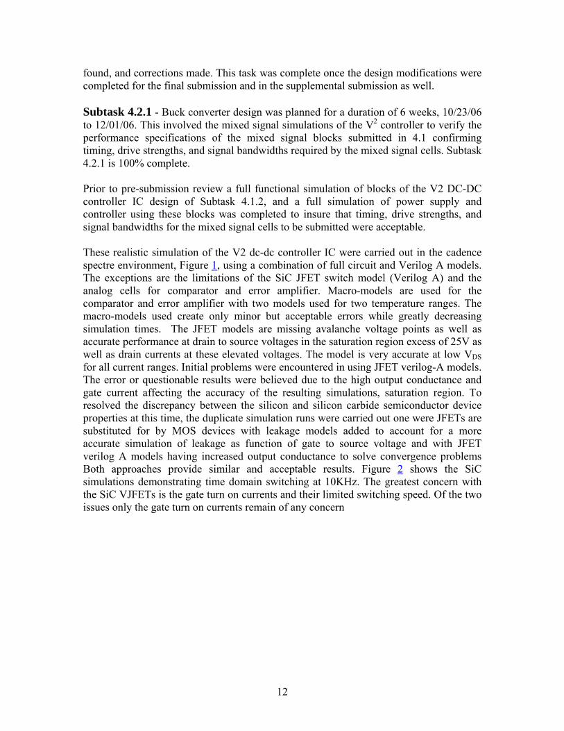
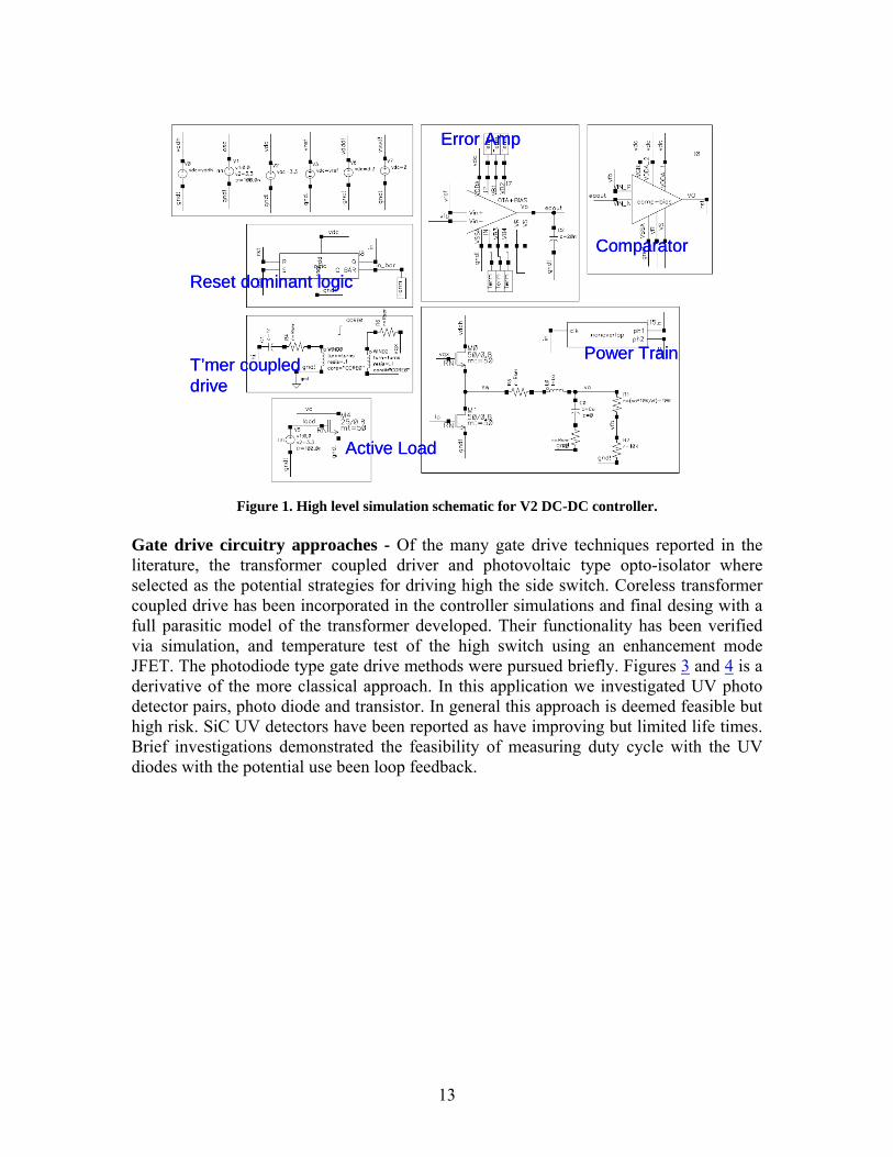
found, and corrections made. This task was complete once the design modifications were completed for the final submission and in the supplemental submission as well. Subtask 4.2.1 - Buck converter design was planned for a duration of 6 weeks, 10/23/06 to 12/01/06. This involved the mixed signal simulations of the V2 controller to verify the performance specifications of the mixed signal blocks submitted in 4.1 confirming timing, drive strengths, and signal bandwidths required by the mixed signal cells. Subtask 4.2.1 is 100% complete. Prior to pre-submission review a full functional simulation of blocks of the V2 DC-DC controller IC design of Subtask 4.1.2, and a full simulation of power supply and controller using these blocks was completed to insure that timing, drive strengths, and signal bandwidths for the mixed signal cells to be submitted were acceptable. These realistic simulation of the V2 dc-dc controller IC were carried out in the cadence spectre environment, Figure 1, using a combination of full circuit and Verilog A models. The exceptions are the limitations of the SiC JFET switch model (Verilog A) and the analog cells for comparator and error amplifier. Macro-models are used for the comparator and error amplifier with two models used for two temperature ranges. The macro-models used create only minor but acceptable errors while greatly decreasing simulation times. The JFET models are missing avalanche voltage points as well as accurate performance at drain to source voltages in the saturation region excess of 25V as well as drain currents at these elevated voltages. The model is very accurate at low VDS for all current ranges. Initial problems were encountered in using JFET verilog-A models. The error or questionable results were believed due to the high output conductance and gate current affecting the accuracy of the resulting simulations, saturation region. To resolved the discrepancy between the silicon and silicon carbide semiconductor device properties at this time, the duplicate simulation runs were carried out one were JFETs are substituted for by MOS devices with leakage models added to account for a more accurate simulation of leakage as function of gate to source voltage and with JFET verilog A models having increased output conductance to solve convergence problems Both approaches provide similar and acceptable results. Figure 2 shows the SiC simulations demonstrating time domain switching at 10KHz. The greatest concern with the SiC VJFETs is the gate turn on currents and their limited switching speed. Of the two issues only the gate turn on currents remain of any concern
12
T’mer coupled drive
Reset dominant logic
Error Amp
Comparator
Power Train
Active Load
T’mer coupled drive
Reset dominant logic
Error Amp
Comparator
Power Train
Active Load
T’mer coupled drive
Reset dominant logic
Error Amp
Comparator
Power Train
Active Load
Figure 1. High level simulation schematic for V2 DC-DC controller.
Gate drive circuitry approaches - Of the many gate drive techniques reported in the literature, the transformer coupled driver and photovoltaic type opto-isolator where selected as the potential strategies for driving high the side switch. Coreless transformer coupled drive has been incorporated in the controller simulations and final desing with a full parasitic model of the transformer developed. Their functionality has been verified via simulation, and temperature test of the high switch using an enhancement mode JFET. The photodiode type gate drive methods were pursued briefly. Figures 3 and 4 is a derivative of the more classical approach. In this application we investigated UV photo detector pairs, photo diode and transistor. In general this approach is deemed feasible but high risk. SiC UV detectors have been reported as have improving but limited life times. Brief investigations demonstrated the feasibility of measuring duty cycle with the UV diodes with the potential use been loop feedback.
13
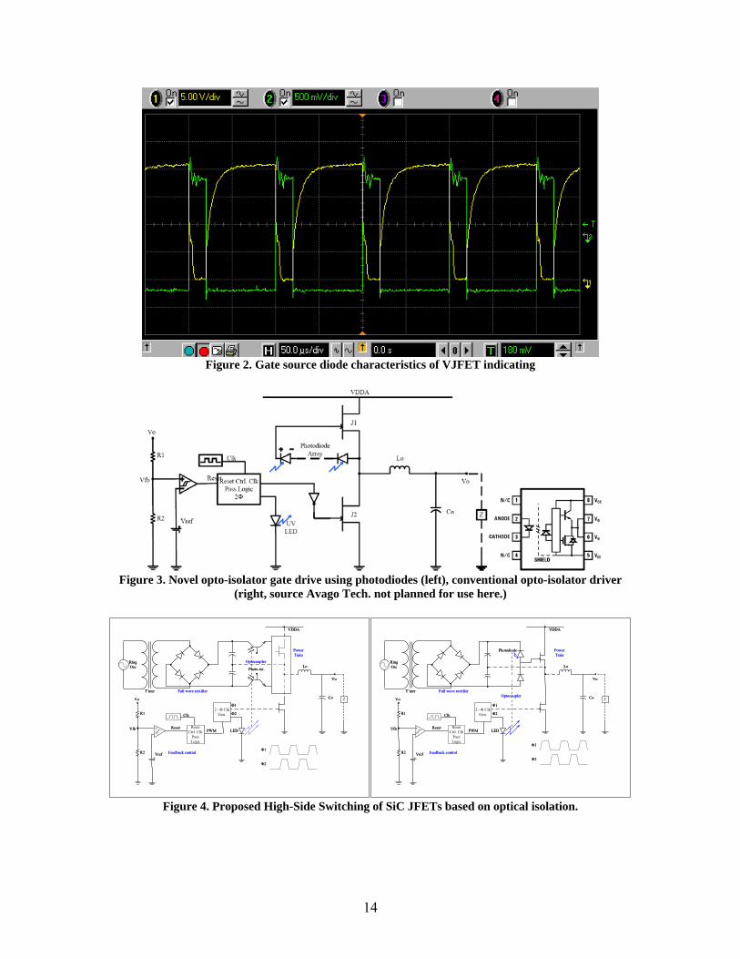
Figure 2. Gate source diode characteristics of VJFET indicating
Figure 3. Novel opto-isolator gate drive using photodiodes (left), conventional opto-isolator driver
(right, source Avago Tech. not planned for use here.)
Vo
Lo
CoVo
Vref
Vfb
R1
R2
Reset Ctrl. Clk
Pass Logic
Clk
Reset
2 - Φ Clk Gen.
Φ1
LED
Photo-txr.
Φ2
Full wave rectifier
Optocoupler
Feedback control
Power Train
RingOsc
T’mer
VDDA
Z
Φ1
Φ2
PWM
Vo
Lo
CoVo
Vref
Vfb
R1
R2
Reset Ctrl. Clk
Pass Logic
Clk
Reset
2 - Φ Clk Gen.
Φ1
LED
Photodiode
Φ2
Full wave rectifierOptocoupler
Feedback control
Power Train
RingOsc
T’mer
VDDA
Z
Φ1
Φ2
PWM
Vo
Lo
CoVo
Vref
Vfb
R1
R2
Reset Ctrl. Clk
Pass Logic
Clk
Reset
2 - Φ Clk Gen.
Φ1
LED
Photo-txr.
Φ2
Full wave rectifier
Optocoupler
Feedback control
Power Train
RingOsc
T’mer
VDDA
Z
Φ1
Φ2
PWM
Vo
Lo
CoVo
Vref
Vfb
R1
R2
Reset Ctrl. Clk
Pass Logic
Clk
Reset
2 - Φ Clk Gen.
Φ1
LED
Photodiode
Φ2
Full wave rectifierOptocoupler
Feedback control
Power Train
RingOsc
T’mer
VDDA
Z
Φ1
Φ2
PWM
Figure 4. Proposed High-Side Switching of SiC JFETs based on optical isolation.
14

Subtask 4.2.2 – SiC switch characterization Duration of Task: 3 weeks, 12/4/07 to 12/22/07 Responsible Team: Analog cell design Subtask 4.2.2 is to develop a SPICE model (Verilog A) for the SiC power switches over the temperature range of 25°C to 275°C using experimental data and test methods. The model was used in the simulation with V2 controller to validate the final integration. Subtask 4.2.2 was of 3 weeks in duration. Multiple approaches have been undertaken to characterize the silicon carbide power switches. Pulsed techniques were the most successful. The critical parameters with respect to an accurate switching model are, the gate capacitance (measured directly), turn on voltage and leakage currents (gate and drain), and on resistance. All have been measured and analyzed for 12 devices. Due to limited number of, variability and cost of these devices, no accurate unifying model general can be extracted. Accurate fitting of the limited is possible. There is a high degree of variability in the on set of threshold and variation in the magnitude of the gate current at threshold. We however have established a typical value for CISS (<320pF), and worst case values for gate current (See Figure 5.) and threshold. These data along with others were sufficient to develop the specification for a coreless drive transformer. Our greatest problem is the high degree of parameter variation in the threshold voltage with gate currents the greatest concern. However, with digital switching circuits threshold variation is not a major concern.
(a) (b)
(c) (d)
Figure 5. Input characteristics for the VJFET (a) gate capacitance (b) gate current verses gate to drain voltage (c), gate current verses gate to source voltage (d)
15
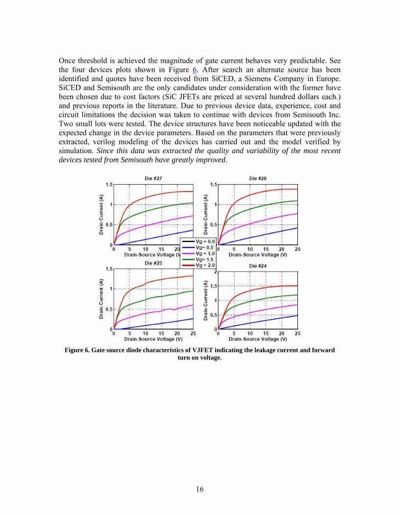
Once threshold is achieved the magnitude of gate current behaves very predictable. See the four devices plots shown in Figure 6. After search an alternate source has been identified and quotes have been received from SiCED, a Siemens Company in Europe. SiCED and Semisouth are the only candidates under consideration with the former have been chosen due to cost factors (SiC JFETs are priced at several hundred dollars each.) and previous reports in the literature. Due to previous device data, experience, cost and circuit limitations the decision was taken to continue with devices from Semisouth Inc. Two small lots were tested. The device structures have been noticeable updated with the expected change in the device parameters. Based on the parameters that were previously extracted, verilog modeling of the devices has carried out and the model verified by simulation. Since this data was extracted the quality and variability of the most recent devices tested from Semisouth have greatly improved.
Figure 6. Gate source diode characteristics of VJFET indicating the leakage current and forward
turn on voltage.
16
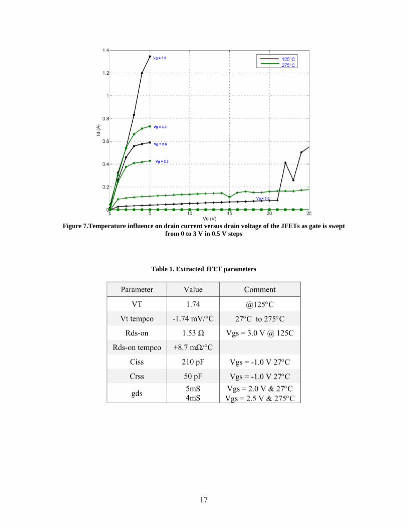
Figure 7.Temperature influence on drain current versus drain voltage of the JFETs as gate is swept
from 0 to 3 V in 0.5 V steps
Table 1. Extracted JFET parameters
Value Comment Parameter
VT 1.74 @125°C
-1.74 mV/°C 27°C to 275°C Vt tempco
Rds-on 1.53 Ω Vgs = 3.0 V @ 125C
+8.7 mΩ/°C Rds-on tempco
Ciss 210 pF Vgs = -1.0 V 27°C
50 pF Vgs = -1.0 V 27°C Crss 5mS 4mS
Vgs = 2.0 V & 27°C Vgs = 2.5 V & 275°C gds
17

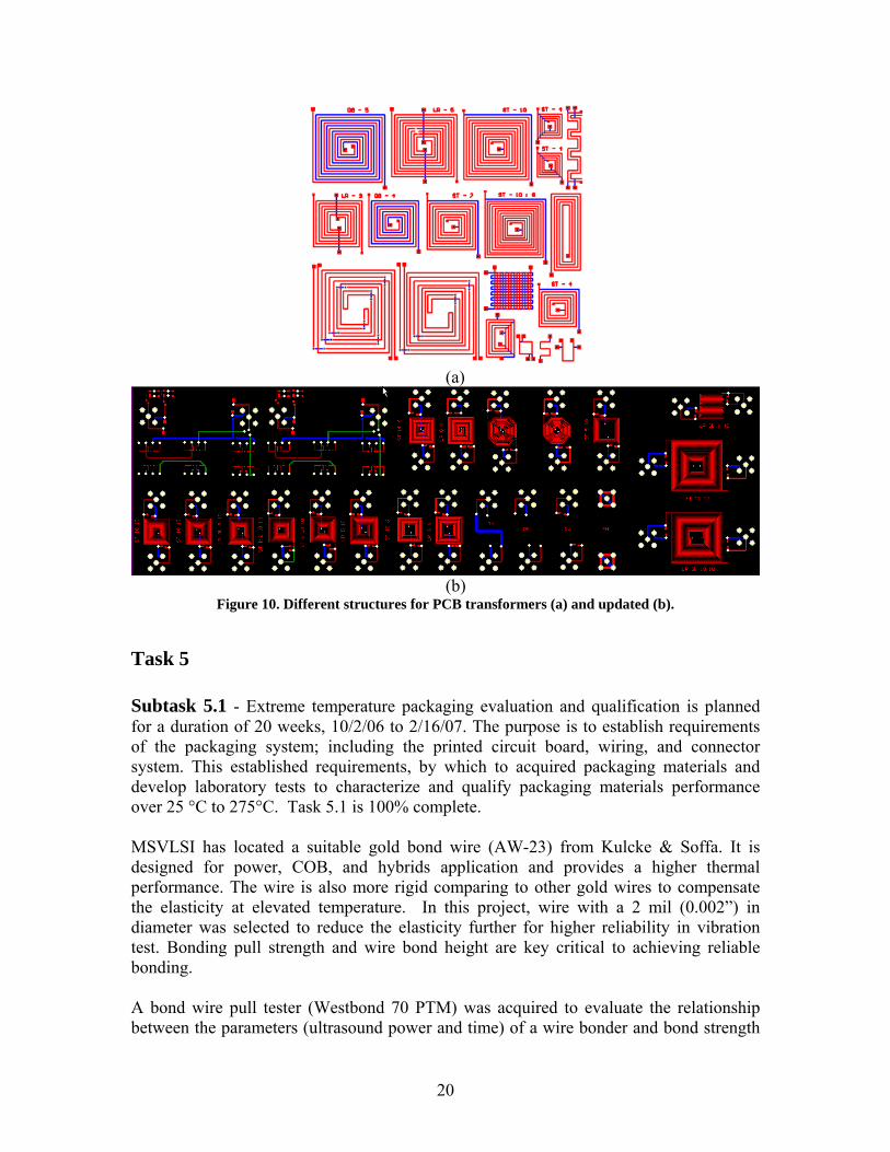
Subtask 4.2.3 - Qualification of discrete devices is planned for a duration of 16 weeks at an expenditure of; DOE $13,086, OSU $602 and is 100% complete. Follows from subtask 4.2.2. Discrete devices – capacitors and inductors were qualified and characterized for electrical and structural properties along with mounting materials. This subtask is intended to produce models of device behavior for selected types of discrete devices, particularly: capacitor dielectric materials, magnetic core materials, and resistor materials using experimental data over the temperature range of 25°C to 275°C. Successfully qualified passive components were used in the SMPS prototypes. The SMPS controller requires capacitors in the following range of values and voltages and an inductor having the following current and resistance specification. Output filters capacitor - 25µF, 50µF and 100µF at 50V (Voltage safety factor of 10). The ESR of this capacitor should be less than 15 milliohms. V2 control compensation - 20nF at 50V or less Output filter inductor - 125µH and 250µH inductors The output voltage ripple and output current affect the final value of capacitance required as does the output current ripple over inductance. The filter network values reported here are for 25V input, 3.3V output, and 25% and 3% current and voltage ripple respectively for 2A converter. Based on literature reviews and personal communications with some high temperature passive component suppliers, the discrete devices have been selected. For load inductors, round copper wire wound on the MPP toroidal core has been selected. Initial tests show very good performance of this type of material over temperature and the inductance remains almost constant (1.2 % reduction) over the range of temperature (25 to 225°C). More tests were carried out to completely validate the suitability of inductors over 275°C range. High temperature series (200°C) low valued capacitors in the range of 220pF and 1nF procured from Kemet has been tested with acceptable performance. These seem to be the preferable and best devices for V2 loop compensation. Again through Personal communications with Kemet an emerging line of integer microfarad capacitors have been identified for test. These capacitors are rated for 260°C which can be extended to 275°C for limited time. This is less of a problem compared to the limited range of capacitance values. A fairly considerable array of these capacitors (3.3µF/unit) is anticipated in the final design for meeting the required capacitance. On the other hand, comparatively lower temperature range, high value capacitors were also tested to find capacitors suitability for short time exposures to higher temperature. The availability of power supply decoupling capacitors for this project is problematic. Also as a part of gate drive circuitry, on-chip and off-chip transformers were analyzed, simulated, laid out, and submitted for fabrication, Figure 10. The transformers of Figure 10 were resubmitted for fabrication to facilitate easy in extracting of there s-parameters. These off-chip counterparts will supplement the on-chip transformers proposed in the
18
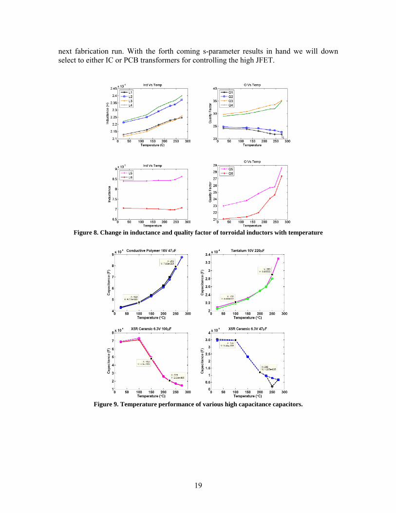
next fabrication run. With the forth coming s-parameter results in hand we will down select to either IC or PCB transformers for controlling the high JFET.
Figure 8. Change in inductance and quality factor of torroidal inductors with temperature
Figure 9. Temperature performance of various high capacitance capacitors.
19
(a)
(b)
Figure 10. Different structures for PCB transformers (a) and updated (b).
Task 5 Subtask 5.1 - Extreme temperature packaging evaluation and qualification is planned for a duration of 20 weeks, 10/2/06 to 2/16/07. The purpose is to establish requirements of the packaging system; including the printed circuit board, wiring, and connector system. This established requirements, by which to acquired packaging materials and develop laboratory tests to characterize and qualify packaging materials performance over 25 °C to 275°C. Task 5.1 is 100% complete. MSVLSI has located a suitable gold bond wire (AW-23) from Kulcke & Soffa. It is designed for power, COB, and hybrids application and provides a higher thermal performance. The wire is also more rigid comparing to other gold wires to compensate the elasticity at elevated temperature. In this project, wire with a 2 mil (0.002”) in diameter was selected to reduce the elasticity further for higher reliability in vibration test. Bonding pull strength and wire bond height are key critical to achieving reliable bonding. A bond wire pull tester (Westbond 70 PTM) was acquired to evaluate the relationship between the parameters (ultrasound power and time) of a wire bonder and bond strength
20
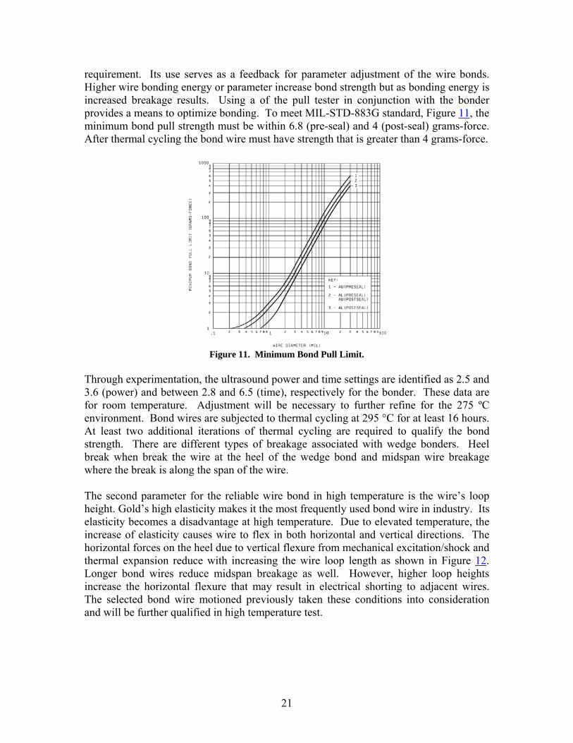
requirement. Its use serves as a feedback for parameter adjustment of the wire bonds. Higher wire bonding energy or parameter increase bond strength but as bonding energy is increased breakage results. Using a of the pull tester in conjunction with the bonder provides a means to optimize bonding. To meet MIL-STD-883G standard, Figure 11, the minimum bond pull strength must be within 6.8 (pre-seal) and 4 (post-seal) grams-force. After thermal cycling the bond wire must have strength that is greater than 4 grams-force.
Figure 11. Minimum Bond Pull Limit.
Through experimentation, the ultrasound power and time settings are identified as 2.5 and 3.6 (power) and between 2.8 and 6.5 (time), respectively for the bonder. These data are for room temperature. Adjustment will be necessary to further refine for the 275 ºC environment. Bond wires are subjected to thermal cycling at 295 °C for at least 16 hours. At least two additional iterations of thermal cycling are required to qualify the bond strength. There are different types of breakage associated with wedge bonders. Heel break when break the wire at the heel of the wedge bond and midspan wire breakage where the break is along the span of the wire. The second parameter for the reliable wire bond in high temperature is the wire’s loop height. Gold’s high elasticity makes it the most frequently used bond wire in industry. Its elasticity becomes a disadvantage at high temperature. Due to elevated temperature, the increase of elasticity causes wire to flex in both horizontal and vertical directions. The horizontal forces on the heel due to vertical flexure from mechanical excitation/shock and thermal expansion reduce with increasing the wire loop length as shown in Figure 12. Longer bond wires reduce midspan breakage as well. However, higher loop heights increase the horizontal flexure that may result in electrical shorting to adjacent wires. The selected bond wire motioned previously taken these conditions into consideration and will be further qualified in high temperature test.
21

Figure 12. Schematic of wire bond flexure during thermal cycling.
The experimental data has demonstrated less flexure in 2 mil compared to 1 mil regular gold wire during the bonding stage. It requires higher loop height to remove any bent formed in the loop. Such conditions become an advantage to overcome horizontal flexure. The useful loop high settings, at room temperature, were identified as being between 6 and 8 relative to the differential height of the die to the selected carrier. To achieve the optimal height, wires will be bonded at loop height settings between 5 and 9. Simultaneous to temperature testing vibration test are scheduled using frequency up to 2000 Hz. This task was completed with chip on board (AlN PCB) assembly of the SMPS controller, JFETs, passives and coreless transformer into functional power. After debug the board will be tested at 295 ºC environment high temperature to confirm bond strength. Subtask 5.2 – Sealing evaluation and qualification. Duration of Task: 8 weeks, 2/19/07 to 4/13/07 Responsible Team: Mixed signal control Planned Expenditure: DOE $8,615 OSU $29,590 The hermitic sealing process is performed inside Nitrogen rich, humidity controlled glove box. The mixture of Helium in the box is required for final leak testing of the seal. Before sealing, the opened bonded chips and lid are baked at 125°C in the vacuum chamber to drive the moisture trapped in the surface of the metals. The chamber is backfilled with Nitrogen once to flush out vaporized materials and then bake in a vacuum a second time. The baked chips are sealed using the parallel seam sealer in the controlled environment. The sealing process is identical to the welding except power setting and additional solder sandwiched between lids and chips. The power level setting for soldering is 800Watt and welding is 2000Watt for the selected package. Selected settings need further adjustments for the selected package and selected solder and re-verification via Helium leak testing.
22
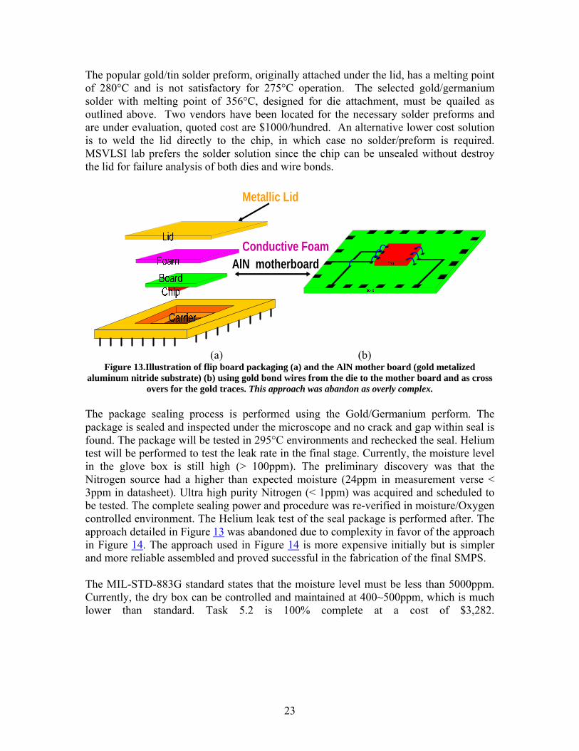
The popular gold/tin solder preform, originally attached under the lid, has a melting point of 280°C and is not satisfactory for 275°C operation. The selected gold/germanium solder with melting point of 356°C, designed for die attachment, must be quailed as outlined above. Two vendors have been located for the necessary solder preforms and are under evaluation, quoted cost are $1000/hundred. An alternative lower cost solution is to weld the lid directly to the chip, in which case no solder/preform is required. MSVLSI lab prefers the solder solution since the chip can be unsealed without destroy the lid for failure analysis of both dies and wire bonds.
Metallic Lid
Conductive FoamAlN motherboard
(a) (b)
Figure 13.Illustration of flip board packaging (a) and the AlN mother board (gold metalized aluminum nitride substrate) (b) using gold bond wires from the die to the mother board and as cross
overs for the gold traces. This approach was abandon as overly complex. The package sealing process is performed using the Gold/Germanium perform. The package is sealed and inspected under the microscope and no crack and gap within seal is found. The package will be tested in 295°C environments and rechecked the seal. Helium test will be performed to test the leak rate in the final stage. Currently, the moisture level in the glove box is still high (> 100ppm). The preliminary discovery was that the Nitrogen source had a higher than expected moisture (24ppm in measurement verse < 3ppm in datasheet). Ultra high purity Nitrogen (< 1ppm) was acquired and scheduled to be tested. The complete sealing power and procedure was re-verified in moisture/Oxygen controlled environment. The Helium leak test of the seal package is performed after. The approach detailed in Figure 13 was abandoned due to complexity in favor of the approach in Figure 14. The approach used in Figure 14 is more expensive initially but is simpler and more reliable assembled and proved successful in the fabrication of the final SMPS. The MIL-STD-883G standard states that the moisture level must be less than 5000ppm. Currently, the dry box can be controlled and maintained at 400~500ppm, which is much lower than standard. Task 5.2 is 100% complete at a cost of $3,282.
23

Packaging solution Commercially available hermetic alumina based ceramic packages are fixed in size and pin count and are in mass production. For packaging single function low power SOI dies (Op-Amp, Comparator, Hysteresis Comparator, Voltage Reference), these packages are readily available at low cost. For packaging DC-DC converter, no suitable hybrid package solution exists due to non-traditional size and pin count. For a solution we must be to turn to a ‘customization package’. It is extremely expensive to customize a package and with labor cost far exceeding the cost of material. Adding to the concern is the high power heat generation from SiC. AlN with its excellent heat conduction properties (140 W/m/°K), compared to alumina (18 W/m/°K), was selected. High thermal conductivity helps to spread heat faster, hence helps to reduce temperature build up in transistor junctions and avoid transistor destruction and increasing lifetimes. In addition, the MSVLSI lab group has experience using AlN material to resolve the thermal issues, with high temperature electronics. Since machining an AlN cavity is extremely expensive a two step hybrid packaging methodology is adopted. This hybrid technique involves eutectic / epoxy bonding of SiC JFETs and SOS IC’s and passive components to an AlN motherboard/substrate followed by eutectic attachment of an AlN window frame acting as the side walls forming a protective cavity for the wire bonds and devices. Finally the substrate is capped with a metallic lid on top of the window frame to provide hermetic sealing of the dies. A three dimensional perspective of packaging is given in Figure 14. The actual CAD diagram of the mother board with top (red) and bottom (blue) metallization is shown in Figure 15. A 1.8 sq. inch aluminum nitride planar board will be the motherboard for the prototype design. A 0.48 sq. inch AlN window frame shall be used to hermetically seal the SOS chip and SiC power devices. The load inductors and capacitors will be externally attached to the board using high temperature electrically conductive epoxy. The AlN packaging approached proved to be modestly successful.
Figure 14. Hybrid packaging perspective of controller IC, power devices and other passives on highly
thermally conductive AlN substrate.
24
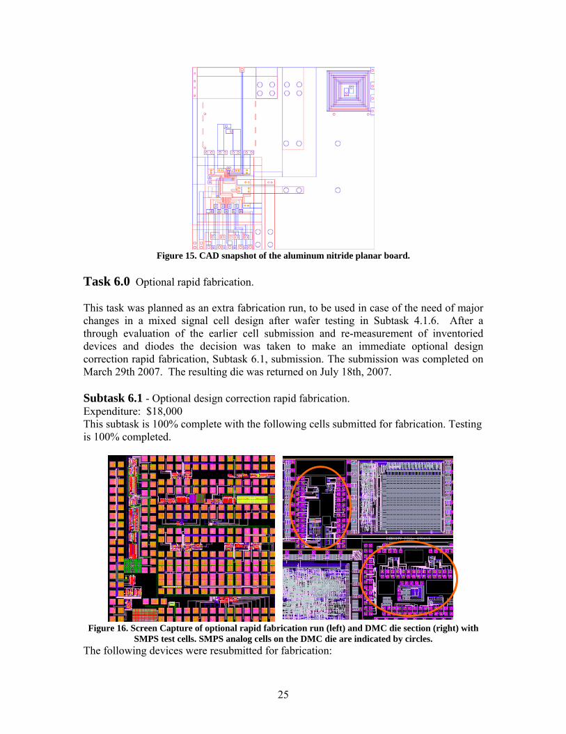
Figure 15. CAD snapshot of the aluminum nitride planar board.
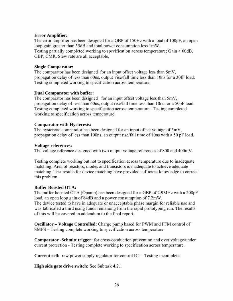
Task 6.0 Optional rapid fabrication. This task was planned as an extra fabrication run, to be used in case of the need of major changes in a mixed signal cell design after wafer testing in Subtask 4.1.6. After a through evaluation of the earlier cell submission and re-measurement of inventoried devices and diodes the decision was taken to make an immediate optional design correction rapid fabrication, Subtask 6.1, submission. The submission was completed on March 29th 2007. The resulting die was returned on July 18th, 2007. Subtask 6.1 - Optional design correction rapid fabrication. Expenditure: $18,000 This subtask is 100% complete with the following cells submitted for fabrication. Testing is 100% completed.
Figure 16. Screen Capture of optional rapid fabrication run (left) and DMC die section (right) with
SMPS test cells. SMPS analog cells on the DMC die are indicated by circles. The following devices were resubmitted for fabrication:
25
Error Amplifier: The error amplifier has been designed for a GBP of 150Hz with a load of 100pF, an open loop gain greater than 55dB and total power consumption less 1mW. Testing partially completed working to specification across temperature; Gain > 60dB, GBP, CMR, Slew rate are all acceptable. Single Comparator: The comparator has been designed for an input offset voltage less than 5mV, propagation delay of less than 60ns, output rise/fall time less than 10ns for a 30fF load. Testing completed working to specification across temperature. Dual Comparator with buffer: The comparator has been designed for an input offset voltage less than 5mV, propagation delay of less than 60ns, output rise/fall time less than 10ns for a 50pF load. Testing completed working to specification across temperature. Testing completed working to specification across temperature. Comparator with Hysteresis: The hysteretic comparator has been designed for an input offset voltage of 5mV, propagation delay of less than 100ns, an output rise/fall time of 10ns with a 50 pF load. Voltage references: The voltage reference designed with two output voltage references of 800 and 400mV. Testing complete working but not to specification across temperature due to inadequate matching. Area of resistors, diodes and transistors is inadequate to achieve adequate matching. Test results for device matching have provided sufficient knowledge to correct this problem. Buffer Boosted OTA: The buffer boosted OTA (Opamp) has been designed for a GBP of 2.9MHz with a 200pF load, an open loop gain of 84dB and a power consumption of 7.2mW. The device tested to have in adequate or unacceptable phase margin for reliable use and was fabricated a third using funds remaining from the rapid prototyping run. The results of this will be covered in addendum to the final report. Oscillator – Voltage Controlled: Charge pump based for PWM and PFM control of SMPS – Testing complete working to specification across temperature. Comparator -Schmitt trigger: for cross-conduction prevention and over voltage/under current protection - Testing complete working to specification across temperature. Current cell: raw power supply regulator for control IC. – Testing incomplete High side gate drive switch: See Subtask 4.2.1
26

High voltage full wave rectifier: Testing incomplete Subtask 6.1 - Optional fabrication, test and revise. Duration of Task: 2 weeks, 7/23/07 to 8/03/07 Responsible Team: Analog cell design Subtask 6.2 – Optional fabrication, test and revise. The recipient shall, upon return of fabricated mixed signal cells from subtask 6.1, submit these cells for wafer testing. The chip was received on July 18, 2007 and still testing. This subtask is 100% complete. Task 7 Integration and packaging of the power supply The recipient shall integrate the mixed signal cells into a fully functional power supply controller IC. A power supply, based upon the V2 controller IC, was designed, devices fabricated, the power supply built and tested over the range of 25 °C to 275 °C. This task consists of subtasks 7.1 through 7.7 will provide for integration of the controller IC, package design, AlN (aluminum nitride) gold board design and fabrication, wafer testing, dice and mount the circuits, package integration of the power supply and test of power supply. Subtask consist of V2 IC controller development, discrete down selection, switching if the power JEFTs, and integration into a hybrid package. Gate drive transformer: Performance of planar printed circuit board transformers fabricated on commercial 4-layer FR4 board was measured in the laboratory. The stacked transformer structure with winding area of 10.5mm x 10.5 mm is found to be the preferred choice. Figure 17 shows the snapshot of the stacked transformer with 10 mil conductor width and 6 mil conductor spacing. The scattering parameters are measured using Agilent 8753ES s-parameter network analyzer. The measured parameters are used to calculate the inductance and the quality factor of the fabricated inductors using the equations 1 and 2 respectively. Figure 18 shows the inductance of the primary winding for a 1 to1 transformer and its quality factor with respect to frequency.
=Lf
Yf
ZL××
⎟⎠⎞
⎜⎝⎛
=××
=ππ 2
1Im
2)Im( [1] )Re(
)Im(ZZQ = [2]
27

Figure 17. Stacked transformer on FR4
printed circuit board.
Figure 18. Measured values of inductance and quality factor for primary winding of a
stacked PCB transformer. For use with the high temperature version of the SMPS converter, layouts shown in Figure 19 were sent out for fabrication as part of the final AIN PCB. These layouts are made to favor self aligned assembly of the gate drive transformers to the converter motherboard. The [10 10 8] layout (right) was expected to have lower interwidning capacitance, hence higher bandwidth compared to the [10 6 10] layout (left). However, the measured differences in parasitic capacitance proved in consequential.
Figure 19. CAD snapshot of the PCB gate drive transformers.
Subtask 7.1 – Integration of controller IC In this subtask the mixed signal cells will be integrated into a fully function power supply controller IC. This task is 100% complete. Subtask 7.1.1 – Integration of mixed signal cells into controller IC. Duration of Task: 6 weeks, 7/9/07 to 8/17/07 Responsible Team: Analog cell design, Mixed signal control Follows from subtask 4.1.6. The final versions of the mixed signal cell designs were integrated into a V2 integrated circuit design for a complete supply controller IC. These mixed signal cell design include the comparator without hysteresis, comparator with hysteresis, operational transconductor amplifier (OTA) or error amplifier, voltage reference and digital logic including ancillary protection circuits, i.e over temperature. Simulations were conducted to verify the full functional design of the controller IC. The task is 100%.
28
The ICs to be delivered in the SMPS project include; the V^2 Controller IC, a dual comparator, voltage reference, a hysteretic comparator and a CMOS opamp. All are presented below were the package pin out, IC layout and a brief performance specification are summarized. An August fabrication run submission was made making minor changes in the V2 controller. The return of this in October will be followed up a supplemental report in the December time frame.
Voltage Reference: A voltage reference is required to establish a reference voltage for the error amplifier in the SMPS controller for accurate setting of output. In principle, a temperature independent reference voltage is generated by combining two voltages of opposite temperature coefficients. A current mode voltage reference was developed and tested capable of generating reference voltages of 400mV and 800mV respectively. These values of reference voltages have been chosen keeping in consideration the common mode voltage range of the error amplifier which has a PMOS input stage and voltage reference performance. In principle a CTAT (complementary to absolute temperature) current, developed across resistor LR and a PTAT (proportional to absolute temperature) current developed are combined across R to generate a temperature independent current and it is mirrored across resistors NR to generate the desired reference voltage. MOS-gated diodes have been used in the design of this voltage reference to establish the required p-n junction. The circuit diagram is shown in Figure 20. The current through resistor R is given by equation 3. Where n = 1.6273, VT = 26mV, K =8 (ratio of diode areas). Using gated diode data and selecting a room temperature current value which will remain in the permissible log linear range (across temperature) results in a selected current value of 127µA. The desired value of R was found to be equal to 689Ω. The reference voltage for the above circuit can be expressed by equation 4.
RKnVTI PTAT
ln= [3] 1ln DREF V
LNknVTNV += [4]
The value of L was calculated by taking the derivative of equation 4 and setting it equal to zero. Using L equals 5; N is solved for using equation 2. A measured plot of the VREF versus temperature is given in Figure 21. The measured temperature coefficient over the entire range (27 to 275 °C) was found to be 143µV/°C. The circuit area including bond pads is 0.4 mm2. Figure 22 shows the packaged chip with the pin assignments along with a block diagram for the voltage reference. The buffer in Figure 22 is a scaled version of error amplifier described below, and is not included in the on chip version of the voltage reference. Only the packaged version includes a buffer. The selection of a folded cascode for the buffer guarantees reference buffer stability across all capacitive loads. At 3.3V, reference supply current is less than 2.6µA across the full temperature range. The PTAT current leg was add and impress across the appropriate resistor to develop a temperature dependent voltage where the 290 °C +/- 10°C voltage equals 400mV.
29

Figure 20. Schematic of the voltage reference.
Figure 21. Plot of reference voltage versus temperature.
(a) (b)
Figure 22. Packaged die of the voltage reference along with pin assignments.
30

Error Amplifier The error amplifier is also a critical building block of the DC-DC V2-squared controller. It compares the scaled output voltage with a reference voltage to produce an output which will be used by the comparator for stabilizing the control loop. The schematic of the proposed error amplifier is shown in Figure 23. Since the generated reference voltage is around 400mV, a PMOS differential pair is chosen. Based on the stability requirements of the control loop, the error amp has been designed for a GBP of 300Hz with a 15 nF load, an open loop gain greater than 60dB, and a slew rate of 300mV/µS across the full temperature range(-25 to 275°C) . The compensation capacitor planned for use in the SMPS control loop is 15nF.
Figure 23. Schematic of the error amplifier.
rom the requirements for the GBP, offset and a selected overdrive voltage of Fapproximately 200mV, the size of the input pair devices was found to be W/L = 4 @ 6µ/12µ. Again a folded current architecture along with additional cascoding has been selected to ensure adequate gain. Operating at lower common mode voltages around 200mV (in the absence the boost OTA) can force transistor M0 in the triode region. This can severely affect the output impedance and voltage gain of the OTA. A feedback boost amp compensates for the anticipated loss of gain/impedance when the output swing forces MC1 into the linear region. The dimensions of the gain boosting amplifier are chosen similar to the input pair and current folding devices of the error amplifier ensuring
31
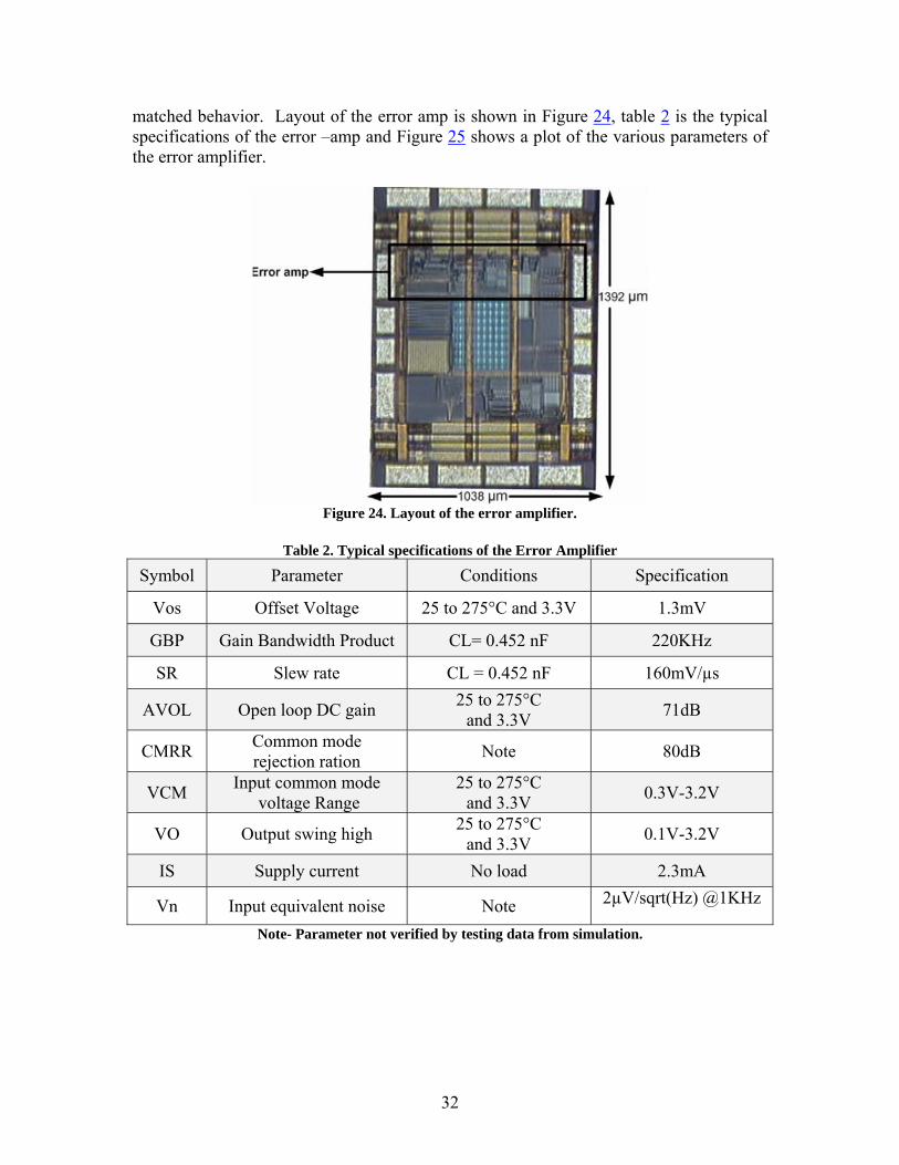
matched behavior. Layout of the error amp is shown in Figure 24, table 2 is the typical specifications of the error –amp and Figure 25 shows a plot of the various parameters of the error amplifier.
Figure 24. Layout of the error amplifier.
Table 2. Typical specifications of the Error Amplifier
32
Symbol Parameter Conditions Specification
Vos Offset Voltage 25 to 275°C and 3.3V 1.3mV
GBP Gain Bandwidth Product CL= 0.452 nF 220KHz
SR Slew rate CL = 0.452 nF 160m V/µs
AVOL 25 to 275°C and 3.3V Open loop DC gain 71dB
CMRR 80dB Common mode rejection ration Note
VCM Inp e ut common mod voltage Range
25 to 275°C 0.3V-3.2V and 3.3V
VO Output swing high 25 to 275°C 0.1V-3.2V and 3.3V IS Supply current No load 2.3mA
Vn Input equivalent noise 2µV/sqrt(Hz) @1KHz Note Note- Parameter not verified by tes ta from simulation.ting da
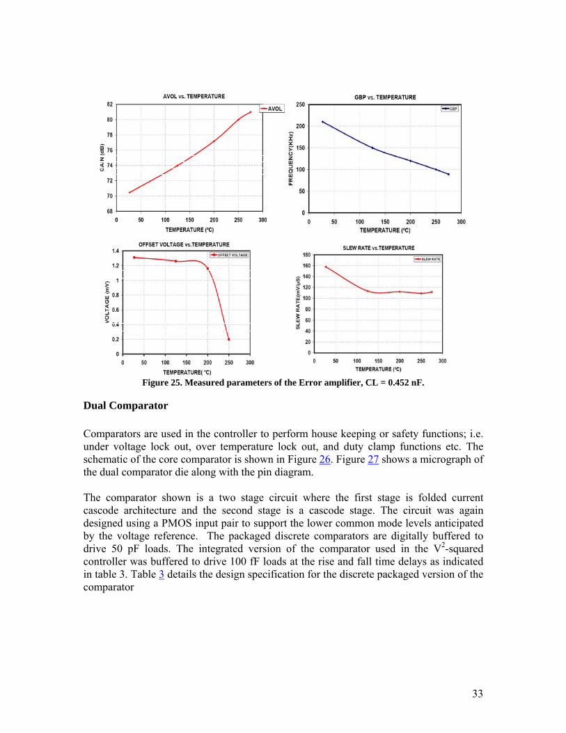
Figure 25. Measured parameters of the Error amplifier, CL = 0.452 nF.
Dual Comparator Comparators are used in the controller to perform house keeping or safety functions; i.e. under voltage lock out, over temperature lock out, and duty clamp functions etc. The schematic of the core comparator is shown in Figure 26. Figure 27 shows a micrograph of the dual comparator die along with the pin diagram. The comparator shown is a two stage circuit where the first stage is folded current cascode architecture and the second stage is a cascode stage. The circuit was again designed using a PMOS input pair to support the lower common mode levels anticipated by the voltage reference. The packaged discrete comparators are digitally buffered to drive 50 pF loads. The integrated version of the comparator used in the V2-squared controller was buffered to drive 100 fF loads at the rise and fall time delays as indicated in table 3. Table 3 details the design specification for the discrete packaged version of the comparator
33
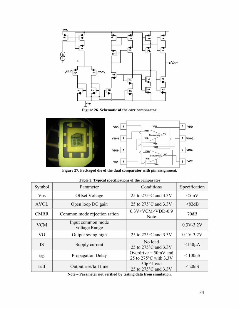
inI
Figure 26. Schematic of the core comparator.
Figure 27. Packaged die of the dual comparator with pin assignment.
Table 3. Typical specifications of the comparator
Parameter Conditions Specification Symbol
Vos Offset Voltage 25 to 275°C and 3.3V <5mV
Open loop DC gain 25 to 275°C and 3.3V <82dB AVOL
CMRR Common mode rejection ration 0.3V<VCM<VDD-0.9 Note 70dB
Input common mode voltage Range 0.3V-3.2V VCM
VO Output swing high 25 to 275°C and 3.3V 0.1V-3.2V
Supply current No load 25 to 275°C and 3.3V <150µA IS
tPD Propagation Delay Overdrive = 50mV and 25 to 275°C with 3.3V < 100nS
Output rise/fall time 50pF Load 25 to 275°C and 3.3V < 20nS tr/tf
Note – Parameter not verified by testing data from simulation.
34

Figure 28. Measured characteristics of the comparator, CL =208pF.
Hysteretic Comparator The hysteretic comparator consists of the core comparator as described in the previous section along with a set–reset NAND latch to provide hysteresis. In the integrated version of the DC-DC controller the hysteretic comparator is used for house keeping functions; under voltage lock out over current and over temperature etc. . The threshold voltages, Vhigh and Vlow are provided using an external resistor divider network in the packaged devices while both internal and external resistors may be used for the SMPS die. The reset pin (CLR) should be tied high, to VDD. Packaged die photo, pin assignments and the measured hysteretic curve versus temperature are shown in Figure 29, Figure 30 and performance specifications in table 4.
Figure 29. Packaged chip of the hysteretic comparator with pin assignment
35

Table 4. Specifications of the hysteretic comparator.
Parameter Conditions Specification Symbol
Vos Offset Voltage 25 to 275°C and 3.3V <5mV
Minimum Hysteresis Vin<100Hz 25 to 275°C and 3.3V <50mV VHYS
Common mode rejection ratio
0.3V<VCM<VDD-0.9 Note 70dB CMRR
Input common mode voltage Range 25 to 275°C and 3.3V 0.3V-3.2V VCM
VO Output swing high 25 to 275°C and 3.3V 0.1V-3.2V
Supply current No load 25 to 275°C and 3.3V 200µA IS
tPD Propagation Delay Overdrive = 50mV 25 to 275°C and 3.3V < 100ns
Output rise/fall time 50pF Load 25 to 275°C and 3.3V 10ns/10ns tr/tf
Note – Parameter not verified by testing data from simulation.
Figure 30. Example hysteresis plot of the comparator.
36

Subtask 7.1.2 – Pre-submission review. Duration of Task: 2 weeks, 8/20/07 to 8/31/07 Responsible Team: Analog cell design Planned Expenditure: DOE $ 9,794 OSU $1,849 Follows from subtask 7.1.1. Prior to submitting the layout of the full controller IC for final fabrication, an extensive in-house review will be conducted to insure the elimination of errors prior to submission for fabrication. The task is 100% completed. Subtask 7.1.3 – Formalize controller IC test plan Duration of Task: 3 weeks, 7/9/07 to 7/27/07 Responsible Team: System timing integration team V2 controller and SMPS Follows in part from Subtask 4.1.5. Testing procedures for full controller IC is 100% complete.. These tests will verify electrical function, pin electrical characteristics, clock-rate, and temperature range of operation. This work leads to Subtask 7.4.3 below. A copy of the complete test program/plans were provided for review. This formal test plan was finalized on an agreement between the Recipient and the DOE COR prior to testing. The formal test plan was attached as an appendix to the March 08 quarterly report. Test results for the SMSP based on the V2 controller IC developed under this effort is detailed in Appendix B. Subtask 7.1.4 – Revise layout as required Duration of Task: 2 weeks, 9/3/07 to 9/14/07 Responsible Team: Analog cell design, Mixed signal control The design and layout of the controller IC was revised in accordance with the results of the pre-submission review of Subtask 7.1.2 and 7.1.3 and is 100% complete. Subtask 7.1.5 – 2nd fabrication submission Duration of Task: 12 weeks, 9/17/07 to 12/7/07 Responsible Team: Mixed signal control The layouts for the full controller IC and spin off ICs (the additional IC’s, comparator, voltage reference, etc. occupied space on the wafer not used by the SMPS controller die) were submitted for fabrication and have been received and tested. This task is 100% complete. --MILESTONE 2a: FULL WAFER SUBMISSION OF SMPS CONTROLLER IC PLUS MIXED SIGNAL CELLS 100% complete.
37
3.0 SMPS testing results
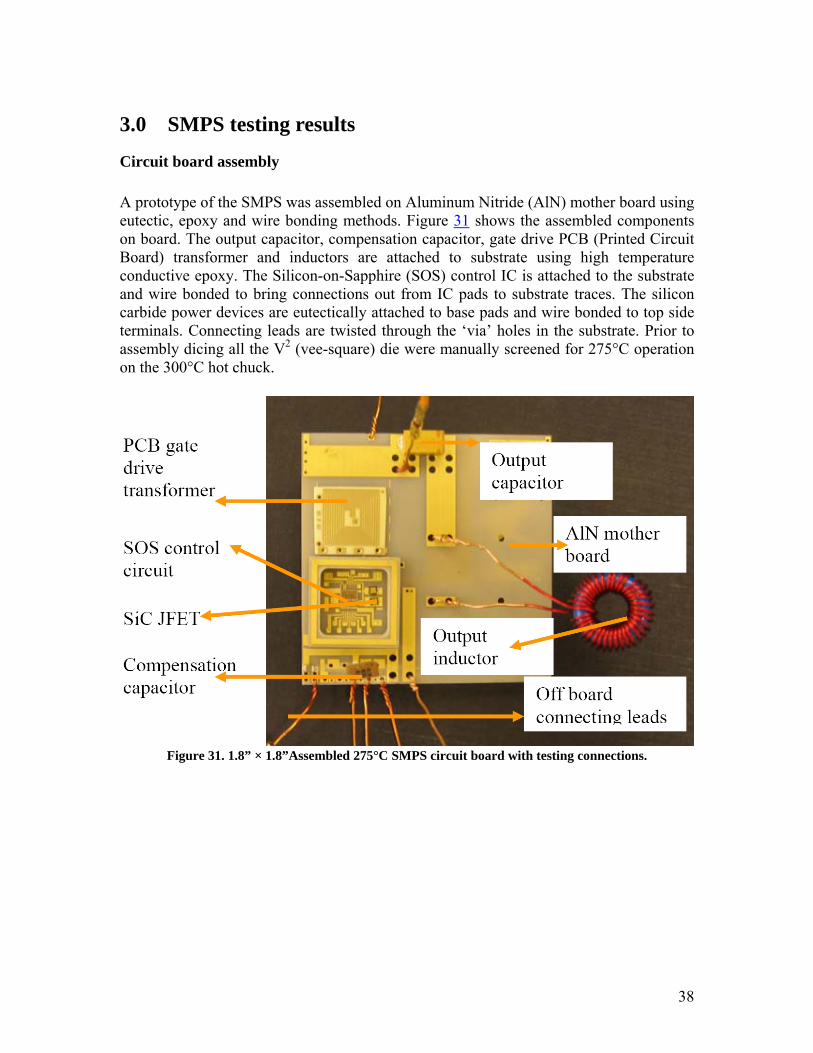
Circuit board assembly A prototype of the SMPS was assembled on Aluminum Nitride (AlN) mother board using eutectic, epoxy and wire bonding methods. Figure 31 shows the assembled components on board. The output capacitor, compensation capacitor, gate drive PCB (Printed Circuit Board) transformer and inductors are attached to substrate using high temperature conductive epoxy. The Silicon-on-Sapphire (SOS) control IC is attached to the substrate and wire bonded to bring connections out from IC pads to substrate traces. The silicon carbide power devices are eutectically attached to base pads and wire bonded to top side terminals. Connecting leads are twisted through the ‘via’ holes in the substrate. Prior to assembly dicing all the V2 (vee-square) die were manually screened for 275°C operation on the 300°C hot chuck.
Figure 31. 1.8” × 1.8”Assembled 275°C SMPS circuit board with testing connections.
38
39
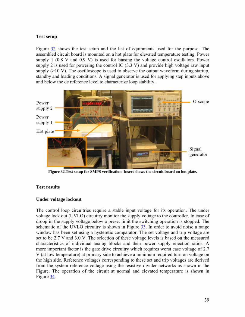
Test setup Figure 32 shows the test setup and the list of equipments used for the purpose. The assembled circuit board is mounted on a hot plate for elevated temperature testing. Power supply 1 (0.8 V and 0.9 V) is used for biasing the voltage control oscillators. Power supply 2 is used for powering the control IC (3.3 V) and provide high voltage raw input supply (>10 V). The oscilloscope is used to observe the output waveform during startup, standby and loading conditions. A signal generator is used for applying step inputs above and below the dc reference level to characterize loop stability.
Figure 32.Test setup for SMPS verification. Insert shows the circuit board on hot plate.
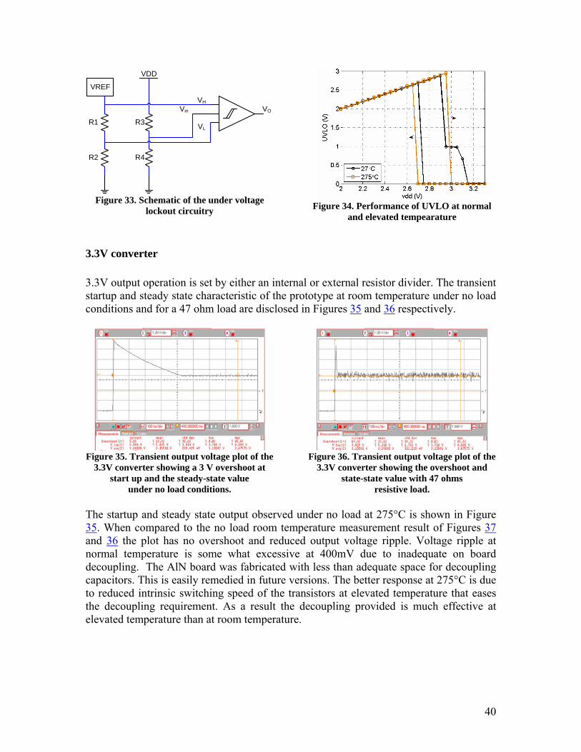
Test results Under voltage lockout The control loop circuitries require a stable input voltage for its operation. The under voltage lock out (UVLO) circuitry monitor the supply voltage to the controller. In case of droop in the supply voltage below a preset limit the switching operation is stopped. The schematic of the UVLO circuitry is shown in Figure 33. In order to avoid noise a range window has been set using a hysteretic comparator. The set voltage and trip voltage are set to be 2.7 V and 3.0 V. The selection of these voltage levels is based on the measured characteristics of individual analog blocks and their power supply rejection ratios. A more important factor is the gate drive circuitry which requires worst case voltage of 2.7 V (at low temperature) at primary side to achieve a minimum required turn on voltage on the high side. Reference voltages corresponding to these set and trip voltages are derived from the system reference voltage using the resistive divider networks as shown in the Figure. The operation of the circuit at normal and elevated temperature is shown in Figure 34.
VH
VL
Vin VO
VREF
VDD
R1
R2
R3
R4
Figure 33. Schematic of the under voltage
lockout circuitry
Figure 34. Performance of UVLO at normal and elevated tempearature
3.3V converter 3.3V output operation is set by either an internal or external resistor divider. The transient startup and steady state characteristic of the prototype at room temperature under no load conditions and for a 47 ohm load are disclosed in Figures 35 and 36 respectively.
Figure 35. Transient output voltage plot of the
3.3V converter showing a 3 V overshoot at start up and the steady-state value
under no load conditions.
Figure 36. Transient output voltage plot of the
3.3V converter showing the overshoot and state-state value with 47 ohms
resistive load.
The startup and steady state output observed under no load at 275°C is shown in Figure 35. When compared to the no load room temperature measurement result of Figures 37 and 36 the plot has no overshoot and reduced output voltage ripple. Voltage ripple at normal temperature is some what excessive at 400mV due to inadequate on board decoupling. The AlN board was fabricated with less than adequate space for decoupling capacitors. This is easily remedied in future versions. The better response at 275°C is due to reduced intrinsic switching speed of the transistors at elevated temperature that eases the decoupling requirement. As a result the decoupling provided is much effective at elevated temperature than at room temperature.
40

Figure 37.Transient output voltage plot of the 3.3 V converter.
The startup and steady state characteristic of the converter for 47 ohms and 8.2 ohms real loads are shown in Figure 38 and 39, respectively. The absence of overshoot and ripple is readily observed at elevated temperatures. This is a direct result of the reduced switching speed of both the CMOS and SiC devices by roughly a factor of 3 as temperature goes from room temperature to at 275°C. A triple of the decoupling capacitors should serve solve future ripple problems.
Figure 38. Startup characteristic of the 3V
converter with 47 ohm resistive load - 275°C.
Figure 39. Startup characteristic of the 3V
converter with 8.2 ohm resistive load - 275°C.
41

Control loop stability The stability of the control loop can be measured indirectly by application of a step function at the reference input. From network system theory and superposition it can be shown that the application of a step change in load or a voltage step change at the reference input are equivalent. Applying a voltage at the input is both simpler and does not require power devices. By observing control loop response to a step change in input loop stability is evaluated. A signal source is used to apply a +/-50mV step amplitude centered at 400mV to reference voltage input. This is the input to the error amplifier. This corresponds to a +/- 12.5% change in load at the output. An excellent or nearly ideal response is observed at the output as shown in Figure 40. This demonstrates that the control loop phase margin is greater than 75 degrees. Figure 40 is for no load conditions. Note that the rise time is the loop’s response to an increase in load and responds without overshoot while the fall time is limited by the no load RC time constant.
SS
(a)
Figure 40. Simplified control loop with equivalent circuit (a) and output transient response to a
12.5% output referred change by pulsing the 400mV voltage reference with a 350 to 450 mV pulse train.
42

The 5V module Similar to the 3.3 V module, a 5V module was also developed and tested. The output voltage in this case is set by the pre-designed internal resistor dividers. Due an undetermined error in the resistance divider value, the obtained output level is lower than the desired level. Of the sets of internal resistor values both can be measured form the die pins. This resistors measured within process tolerance. Additionally the resistor pairs for each voltage set resistor pair were interdigitated to improve accuracy as well as LVS’ed and otherwise double checked for design and layout errors. We could not determine any reason for the error and as a result we are lost to explain the result. Externally added resistors demonstrated proper SMPS operation as noted above. The start up and steady state response of the converter under no load and with 47 ohm load is shown in Figure 41 and 42 respectively. Again at room temperature we have observed an overshoot at start up. In the 5V case slightly greater than 2 volts.
Figure 41. Transient output voltage plot of the
5 V converter showing a 2 V overshoot at start up an the steady-state value under no
load conditions.
Figure 42. Transient output voltage plot of the
5 V converter showing a 2 V overshoot at start up and the steady-state value under a
load of 47 ohms. Again control loop stability is tested for and observed using the same technique described above for the 3.3 V converter. A response somewhat less than a critically damped loop response is shown in Figure 43. Note that for the test of Figure 43 is under no load conditions and again from the rise response we observe that the loop is stable and phase margin is greater than 75 degrees. The fall response is again dictated by the no load RC time constant. Note that the V2 controller has a rapid response to power demands but responds slowly to decreased power demands.
Figure 43. Control loop behavior for step +/- 100 mV step change applied at the reference input of the 5V SMPS module under no load
conditions.
43
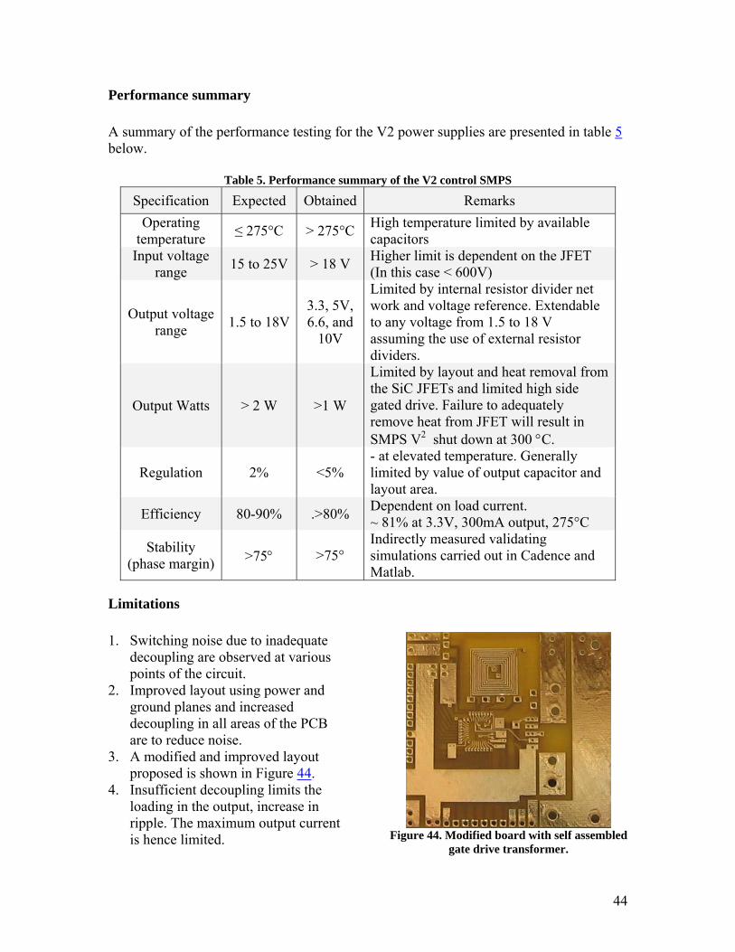
Performance summary A summary of the performance testing for the V2 power supplies are presented in table 5 below.
Table 5. Performance summary of the V2 control SMPS
Specification Expected Obtained Remarks Operating
temperature ≤ 275°C > 275°C High temperature limited by available capacitors
Input voltage range 15 to 25V > 18 V Higher limit is dependent on the JFET
(In this case < 600V)
Output voltage range 1.5 to 18V
3.3, 5V, 6.6, and
10V
Limited by internal resistor divider net work and voltage reference. Extendable to any voltage from 1.5 to 18 V assuming the use of external resistor dividers.
Output Watts > 2 W >1 W
Limited by layout and heat removal from the SiC JFETs and limited high side gated drive. Failure to adequately remove heat from JFET will result in SMPS V2 shut down at 300 °C.
Regulation 2% <5% - at elevated temperature. Generally limited by value of output capacitor and layout area.
Efficiency 80-90% .>80% Dependent on load current. ~ 81% at 3.3V, 300mA output, 275°C
Stability (phase margin) >75° >75°
Indirectly measured validating simulations carried out in Cadence and Matlab.
Limitations 1. Switching noise due to inadequate
decoupling are observed at various points of the circuit.
2. Improved layout using power and ground planes and increased decoupling in all areas of the PCB are to reduce noise.
3. A modified and improved layout proposed is shown in Figure 44.
4. Insufficient decoupling limits the loading in the output, increase in ripple. The maximum output current is hence limited.
Figure 44. Modified board with self assembled
gate drive transformer.
44

Conclusions The performance of the V2 controller implemented in SOS is verified with the silicon carbide power switches and passive high temperature components, R and C’s. Prototype converters for 3.3 V and 5 V output were developed and their performances measured under startup and loaded conditions are disclosed at room temperature and at 275°C. The prototypes are built on the custom made 1.8 sq. inch aluminum nitride substrates with thin film gold metallization. Excellent performance is obtained at higher temperatures. External control of the duty cycle limit and non overlapping periods is provided to the user. Several other user programmable and debugging options such as over current protection, high temperature indicator, controller status indicator etc. are provided, see appendix B. With minor improvements to the preliminary design the V2 control SMPS IC or the complete converter can be made commercially available for an estimated cost as given below in table 6.
Table 6. Cost estimation for commercial 275°C SMPS.
Component Estimated Cost (USD)
SOS control IC 200
AlN package 300
Capacitor 100
Bonding accessories 100
Gate drive transformer 10
Inductor 5
Sub total 715
SiC devices 300
Overhead 200
Total 1215
45

46
Miscellaneous
1. Though the SMPS is designed as a synchronously switching converter, the low side switch can be replaced with a silicon carbide diode to reduce system cost.
2. The V2 control IC has general purpose use and may also be used for other types of converters such as boost and flyback type converters.
Technology transfer A list of papers presented on basis of this research is presented below.
1. V. Madhuravasal, S. Venkataraman, C.-M. Liu, and C. Hutchens, "Extreme Temperature Switch Mode Power Supply based on Vee-square Control Using SiC, Si on Sapphire, Hybrid Technology," in IMAPS International Conference and Exhibition on High Temperature Electronics, Albuquerque, New Mexico, USA, 2008.
2. V. Madhuravasal, P. Kota, and C. Hutchens, "Efficient Gate Drive Mechanism for Novel Silicon Carbide Power FETs," in 41st International Symposium on Microelectronics Rhode Island, USA 2008.
Technical notes and future plans Test plans were completed earlier on the 5 IC to be delivered the V2 controller and the 4 mixed signal ICs; Operational Transconductance Amplifiers, Comparators, Voltage Reference. The building block IC data sheets are detailed in Appendix A. See Task 6.1. The test procedures were provided and documented in previous quarterly reports. The resulting tested and packaged die along with appropriate data sheets have been submitted along with this final report. Two version of the SMPS controller have been implemented on an AlN PCB with favorable results. Test results are presented above. A 3rd generation of the V2-squared controller IC was submitted in August for fabrication and is due out mid October. This along with a polyamide PCB will be used to implementation a 240 °C SMPS. The third V2-squared controller IC will be tested in the October-December time frame and will results to be reported in a follow up addendum to this report.
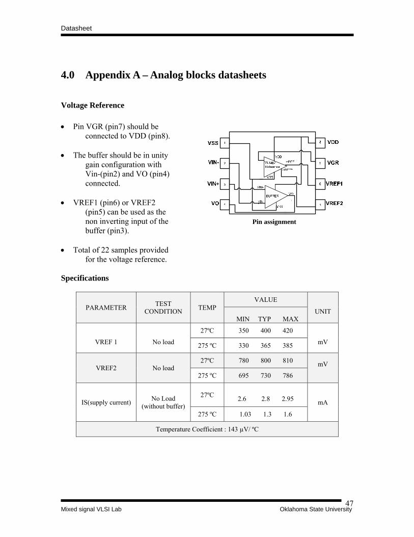
Datasheet
Mixed signal VLSI Lab Oklahoma State University 47
4.0 Appendix A – Analog blocks datasheets
Voltage Reference • Pin VGR (pin7) should be
connected to VDD (pin8). • The buffer should be in unity
gain configuration with Vin-(pin2) and VO (pin4) connected.
• VREF1 (pin6) or VREF2
(pin5) can be used as the non inverting input of the buffer (pin3).
• Total of 22 samples provided
for the voltage reference.
Pin assignment
Specifications
PARAMETER TEST CONDITION TEMP
VALUE UNIT
MIN TYP MAX
VREF 1
No load
27ºC 350 400 420 mV 275 ºC 330 365 385
VREF2 No load 27ºC 780 800 810 mV
275 ºC 695 730 786
IS(supply current) No Load (without buffer)
27ºC
2.6 2.8 2.95 mA
275 ºC 1.03 1.3 1.6
Temperature Coefficient : 143 µV/ ºC

Datasheet
Mixed signal VLSI Lab Oklahoma State University 48
Error amplifier • The buffer provided along
with the Voltage reference is the error amplifier. The buffer serves the functions of both error amplifier and buffer.
Pin assignmentSpecifications
PARAMETER TEST CONDITION TEMP
VALUE UNIT MIN TYP MAX
Vos(offset voltage) No Load
27ºC 1.0 1.3 2.5 mV 275 ºC 0.2
GBP(gain bandwidth product)
CL= 0.452 nF
27ºC 220 KHz 275 ºC 90
IS(supply current) No Load
27ºC 2.3 mA 275 ºC
1.3
AVol(Open loop Gain) No Load
27ºC 71
dB 275 ºC 81
CMRR (Common mode rejection ratio)
27 ºC 120 dB
VCM (Input common
mode voltage range) 27 ºC 0.3-2.2 V
VO(Output swing high) 27 ºC 0.1-3.1 V
Vn(Input equivalent noise) 27 ºC 2 HzV /μ
SR(Slew rate) CL= 0.452 nF
27 ºC 160 mV/µS
275 ºC 115
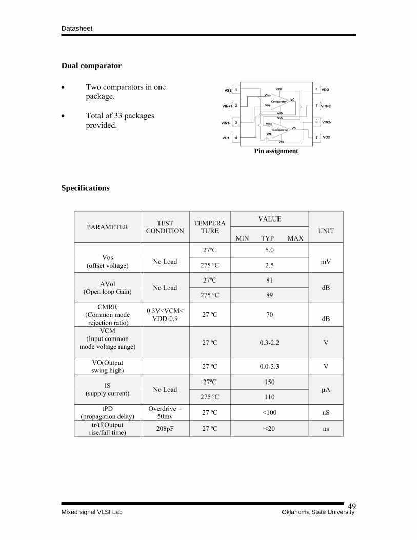
Datasheet
Mixed signal VLSI Lab Oklahoma State University 49
Dual comparator • Two comparators in one
package. • Total of 33 packages
provided.
Pin assignment
Specifications
PARAMETER TEST CONDITION
TEMPERATURE
VALUE UNIT
MIN TYP MAX
Vos
(offset voltage)
No Load
27ºC 5.0 mV 275 ºC 2.5
AVol (Open loop Gain) No Load
27ºC 81 dB
275 ºC 89
CMRR (Common mode rejection ratio)
0.3V<VCM<VDD-0.9 27 ºC 70
dB
VCM (Input common
mode voltage range)
27 ºC 0.3-2.2 V
VO(Output swing high) 27 ºC 0.0-3.3 V
IS (supply current) No Load
27ºC 150 µA
275 ºC 110
tPD (propagation delay)
Overdrive = 50mv 27 ºC <100 nS
tr/tf(Output rise/fall time) 208pF 27 ºC <20 ns

Datasheet
Mixed signal VLSI Lab Oklahoma State University 50
Hysteretic comparator • QB is the inverted
output of Q. • Vhigh and Vlow are
used to set the threshold limits of the hysteresis.
• CLR should be
connected to VDD. • A total of 28 packages
have been provided.
Pin assignment
Specifications
PARAMETER TEST CONDITION TEMP
VALUE UNIT
MIN TYP MAX
Vos
(offset voltage)
No Load
27ºC 5.0 mV 275 ºC 2.5
VHYS (hysteresis) Vin<100Hz
27ºC 25 mV
275 ºC 50
CMRR (Common mode rejection ratio)
0.3V<VCM <VDD-0.9 27 ºC 70
dB
VCM(Input common mode voltage range)
27 ºC 0.3-2.2 V
VO(Output swing high) 27 ºC 0.0-3.3 V
IS(supply current) No Load
27ºC 200 µA
275 ºC 110
tPD (propagation delay)
Overdrive = 50mv 27 ºC <100 nS
tr/tf (Output rise /fall time)
208pF 27 ºC 10/10 nS

5.0 Appendix B
Transfer function of the buck converter loop The loop transfer function of the developed converter is numerical analyzed using equation 5. Based on the design parameters the bode plot showing the magnitude and phase response of the system is obtained from Matlab and is shown in Figure 45. From the phase plot it can be noted that the phase margin is greater than 65°. Hence is justifiable to state that the control loop is stable.
⎥⎦
⎤⎢⎣
⎡++++++++++
+
×
⎥⎥⎥⎥
⎦
⎤
⎢⎢⎢⎢
⎣
⎡
+
+×××−=
)()))()((()()1(
1
1
2onClonlConClC
C
p
zg
RRRLRRRRRRRCsRRLCssCRR
s
s
VAeAcTF
ω
ω
[5]
Figure 45. Expected frequency response of the buck converter loop transfer function.
51
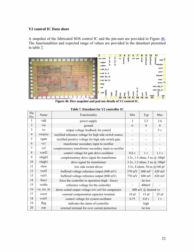
V2 control IC Data sheet A snapshot of the fabricated SOS control IC and the pin-outs are provided in Figure 46. The functionalities and expected range of values are provided in the datasheet presented in table 7.
Figure 46. Dice snapshot and pad out details of V2 control IC.
Table 7. Datasheet for V2 controller IC
vo_res_5v
vo_res_3v
vsource
vgate
bufhiout2
bufhiout1
bufloout
vddh
b2
vddh
hite
mp
ocp
flag
vctr
l1
ccex
t
vo_r
es_i
n
vref
vref
1
initr
st
vctrl2
Pin Name Functionality Min Typ Max No. 1 vdd power supply 3 3.3 3.6 2 vss ground 0 0 0 3 vo output voltage feedback for control - - 5 v 4 vsource rectified reference voltage for high side switch source - - - 5 vgate rectified positive voltage for high side switch gate - - - 6 vs1 transformer secondary input to rectifier - - - 7 vs2 complementary trans - - - former secondary input to rectifier 8 vctrl2 control voltage for gate drive oscillator 0.8 v 1 v 1.1 v 9 vhigh2 complementary r transformer 3. 5 ohm @ drive signal fo 3v, 1. s, 5 ns 100pf
10 v high1 drive s ormer ignal for transf 3.3 1.5 ohm @ f v, s, 5 ns 100p11 v low sid driver 3.3 8 ohms ns @10 f low e switch v, , 50 0 p12 v ref2 buff V) ered voltage reference output (400 m 370 mV 400 mV 42 0 mV13 vref1 buffered voltage reference output (800 mV) 770 mV 800 mV 820 mV 14 force force the controller to operation (high - force) tie w lo15 v 40 V refin reference voltage for the controller - 0m - 16 vo in _res_ down scaled output voltage wrt vref for comparator 400 mV @ esired v d o 17 ccext e 1 xternal compensation capacitor terminal 10 nf 5 nf 25 nf 18 vctrl1 control voltage for system oscillator 0.75 0.8 v 1 v 19 flag in r dicates the status of controlle high 20 ocp external te tection rminal for over current pro tie low
52
53
National Energy Technology Laboratory 626 Cochrans Mill Road P.O. Box 10940 Pittsburgh, PA 15236-0940 3610 Collins Ferry Road P.O. Box 880 Morgantown, WV 26507-0880 One West Third Street, Suite 1400 Tulsa, OK 74103-3519 1450 Queen Avenue SW Albany, OR 97321-2198 2175 University Ave. South Suite 201 Fairbanks, AK 99709 Visit the NETL website at: www.netl.doe.gov Customer Service: 1-800-553-7681