OF QUASI-OPTICAL CIRCUIT TECHNIQUES IN VARACTOR …
124
4 r/) 4 z CONTRACTOR REPORT STUDY OF QUASI-OPTICAL CIRCUIT TECHNIQUES IN VARACTOR MULTIPLIERS by Jesse J. Tunb and Gediminas P. KUT@S Prepared by CUTLER-HAMMER7 INC. Deer Park, Long Island, N. Y. for Electrotzics Research Center NATIONAL AERONAUTICS AND SPACE ADMINISTRATION WASHINGTON, D. C. NOVEMBER 1969
Transcript of OF QUASI-OPTICAL CIRCUIT TECHNIQUES IN VARACTOR …

4 r/)
4 z
C O N T R A C T O R R E P O R T
STUDY OF QUASI-OPTICAL CIRCUIT TECHNIQUES I N VARACTOR MULTIPLIERS
by Jesse J . Tunb and Ged iminas P. KUT@S
Prepared by CUTLER-HAMMER7 INC. Deer Park, Long Island, N. Y . for Electrotzics Research Center
N A T I O N A L A E R O N A U T I C S A N D S P A C E A D M I N I S T R A T I O N W A S H I N G T O N , D . C . N O V E M B E R 1969
NASA CR-1453 TECH LIBRARY KAFB, NM
STUDY OF QUASI-OPTICAL CIEECUIT TECHNIQUES
IN VARACTOR MULTIPLIERS
By J e s s e J. Taub and Gediminas P. Kurpis
Distribution of this report is provided in the interest of information exchange. Responsibility for the contents resides in the author or organization that prepared it.
Prepared under Contract No. NAS 12-625 by
Deer Park, Long Island, N.Y. CUTLER-HAMMER, INC.
for Electronics Research Center
NATIONAL AERONAUTICS AND SPACE ADMINISTRATION
For sale by the Clearinghouse for Federal Scientific and Technical Information Springfield, Virginia 22151 - Price $3.00

TABLE OF CONTENTS
Introduction
Objectives Historical Background General Considerations
Directional Filters
General Experimental Verification Equal Iteration Filter Modified Equal Iteration Filter Low-Ripple (Stepped Impedance) Filter
Tuners
Type 1 Tuner Type 2 Tuner Type 3 Tuner Comparison of Tuner Types
Mechanical Design Considerations (Type 3 Tuner) Additional Tuner Design Problems Concluding Remarks
Varactor Mounting Techniques and Representation
General Remarks Varactor Mounting Techniques Equivalent Circuit Representation
5
5 7 IO 31 46
57
59 65 69
73
75 77 82
83
83
84 89
iii

Measurements
Transitions (Tapers) Mode Conversion VSWR Measurements
Frequency Measurements Power Measurements Loss or Efficiency Measurements
Conclusions
References
Appendix A--Contract Work Statement
Appendix B--Insertion Loss Versus Electrical Length of Iterated Dielectric-Slab Filters
Appendix C--Quasi-Optical Strip Grating Circuit
Appendix D--Matching By Two Variable Susceptances Separated By A Fixed Length
93 95 95
99 99 101
103
105
107
109
113
115
iv

LIST OF ILLUSTRATIONS
Figure
1
2 3 4
5
6 7 8
Basic Quasi-Optical Multiplier Block Diagram Quasi-Optical Directional Filters Response of a Typical Directional Filter Insertion Loss vs Frequency of a Quartz/Air Four- Iteration Directional Filter Iterated Dielectric Slabs with a Linearly Polarized Wave, Incident at an Angle 8i, Whose Electric Vector is Perpendicular to the Plane of Incidence Characteristics of n = 1 Filter Passband and Rejection Band of n = 2 Filter Passband and Rejection Band of n = 3 Filter
11
1 5 16
17 9 Passband and Rejection Band of n = 4 Filter 18 10 Passband and Rejection Band of n = 5 Filter 20 11 Passband and Rejection Band of n = 6 Filter 22
12 7 k o Modes of Doubler Operation 25 13 Maximum Rejection vs Relative Dielectric Constant 27
14 Passband Null Location vs Relative Dielectric Con- 29
in n-Iteration Directional Filters
stant (Use for f = 1/2 Mode) 15 Illustration of the Reference Plane Ambiguity 32 16 Modified Four Quartz/Air Equal Iteration Directional 34
17 Modified Five Quartz/Air Equal Iteration Directional' 38
18 Characteristics of Modified Five Quartz/Air Iteration 45
19 Low Ripple Filter Design Parameters 50
Filter Characteristics
Filter Characteristics
Filter When K = 1.75
V

Figure Page - 20 21
22 23 24 25 26
27 28
29 30 31
32
33
34
35
36
37 38
39 40
41
42 43
44
45
Some Artificial Dielectrics 52 Dielectric Change Factor vs Filling Factor 54
Type 1 Tuner 58 Type 2 Tuner 58 Possible Type 3 Tuner Configuration 59 Equivalent Circuit of a 1 Tuner 60 Type 1 Tuner Characteristics 61 Grating Representation 63
Dissipation of a Movable Susceptance (Type 1) Tuner 64 vs Incidental Shunt Conductance with gL as a Parameter Equivalent Circuit of a Lossless Type 2 Tuner 67 Lossy Type 2 Tuner Representation 67
Type 2 Tuner Losses 68
Type 3 Tuner 70 Normalized Susceptance of Type 3 Tuner v s VSWR 72 Type 3 Tuner Insertion Loss vs VSWR with Tuner 74 Plate &u as a Parameter Side View of Type 3 Tuner 75
Susceptance Variation Principle 76
Face View of Type 3 Tuner 77 Noncontacting Tuner Plate Representation 79
Susceptance Formed on a Substrate 81
Varactor Mounting Techniques 85
Focused Varactor Mounts 86
Fringe Pattern at Focal Plane 87 Frequency Multiplication Process by an Array 90 (Digital Sampler Model)
Tapered Transitions from Standard to Oversized 94 Waveguide Higher Mode Effect on Insertion Loss Measurement 96
vi
Figure Page
46 Use of Tee Junction as a Trapped Mode Filter 97 47 Preferred Method of Reflection Coefficient or VSWR 98
Measurement 48 Interferometer for Frequency Measurements 100
49 Some Loss Measurement Methods 102
vii

STUDY OF QUASI-OPTICAL CIRCUIT TECHNIQUES IN VARACTOR MULTIPLIERS
By Jesse J. Taub and Gediminas P. Kurpis
AIL - a division of CUTLER-HAMMER Deer Park, New York 11729
SUMMARY
Circuit techniques applicable to quasi-optical multipliers operating at millimeter wavelengths have been studied. Direc- tional filters consisting of iterations of dielectric slabs have been theoretically and experimentally investigated. A theory that is in good agreement with experiment is presented together with a step-by-step design procedure. Three types of tuner cir- cuits to be used as impedance matching devices have been theoretically analyzed for their range of matching and dissipa- tion loss properties. The dissipation loss is low (less than 0. 2 db) for all types. A tuner consisting of a variable suscep- tance with variable position is found to be the best of the types described. The problem of representing quasi-optical varactor muunts by suitable equivalent circuits is considered but its com- pletion must await experimental work to be performed on a future program. The report concludes with a discussion of measurement techniques suitable for quasi-optical components.
INTRODUCTION
Objectives
The objectives of this contract are to study quasi-optical circuit tech- niques that are applicable to millimeter wavelength varactor multipliers. More specifically, four problem areas have been defined:
1. Directional filters for separation of fundamental and harmonic frequencies
1
2. Tuners for adjusting the fundamental and harmonic loads to the desired impedance levels
3. Equivalent circuits for quasi-optical varactor m o m t s 4. Measurement techniques applicable to the development
and evaluation of multiplier circuits
The study of these problem areas was performed in accordance with the statement of work given in Appendix A.
Historical Background
The generation of CW millimeter wavelength power with fundamental
solid-state oscillators has been limited to several milliwatts. The achieve-
ment of 10 mw at 88 GHz (reference 1) with bulk gallium arsenide and 100 mw at 100 Ghz with avalanche diodes (reference 2) are representative of the
current state of the art of fundamental oscillators. Solid-state oscillators
yield output powers that drop at a rate of ( l / f ) 2 . Thus, while 1 watt ava- lanche diode oscillators at 30 GHz are feasible (reference 3) , only 250 mw
of power is attainable at 60 GHz. If, for example, a 1-watt 30-GHz oscillator drove a frequency doubler having an efficiency higher than 25 percent, more
60-GHz power would be obtained than from a 60-GHz fundamental oscillator.
Recent advances (reference 4) in varactor diode fabrications have re- sulted in cutoff frequencies in the 800 GHz range with average capacitances of 0.15 pf and selfresonant frequencies of 70 GHz. Assuming no circuit
losses, one can achieve doubler efficiencies (reference 5) for a 30-GHz in-
put of 50 percent; tripling 30 GHz would yield an efficiency of 33 percent. Further advances in cutoff frequency to about 1500 GHz zwe possible which
will result in efficiencies of 70 and 50 percent, respectively.
Unfortunately, the use of these diodes in standard-size millimeter waveguide results in significant circuit losses. The use of highly oversized
(typically ten times larger than standard in each cross-section dimension)
waveguide has been used previously to reduce circuit losses ai: millimeter
2

and submillimeter wavelengths (references 6 - 9). The dominant TEIO mode is preserved in the' oversized guide. The effect of loss rcduction from that of a standard-sized waveguide at 300 GHz illwtrates the degree of loss re- duction attainable.
A number of components using oversized waveguide have been pre-
viously studied (in varying degrees) using quasi-optical elements such as
gratings, prisms, and dielectric plates (slabs); they have been described in references 6 - 9.
These components include:
Double-prism attenuators or couplers Phase shifter using a double prism Tuner o r impedance transformer using a double prism Directional and nondirectional filters using dielectric slabs Grating bandpass filters (nondirectional)
Focused varistor mounts Bolometer mounts Ferrite isolator using Faraday rotation
Tapers
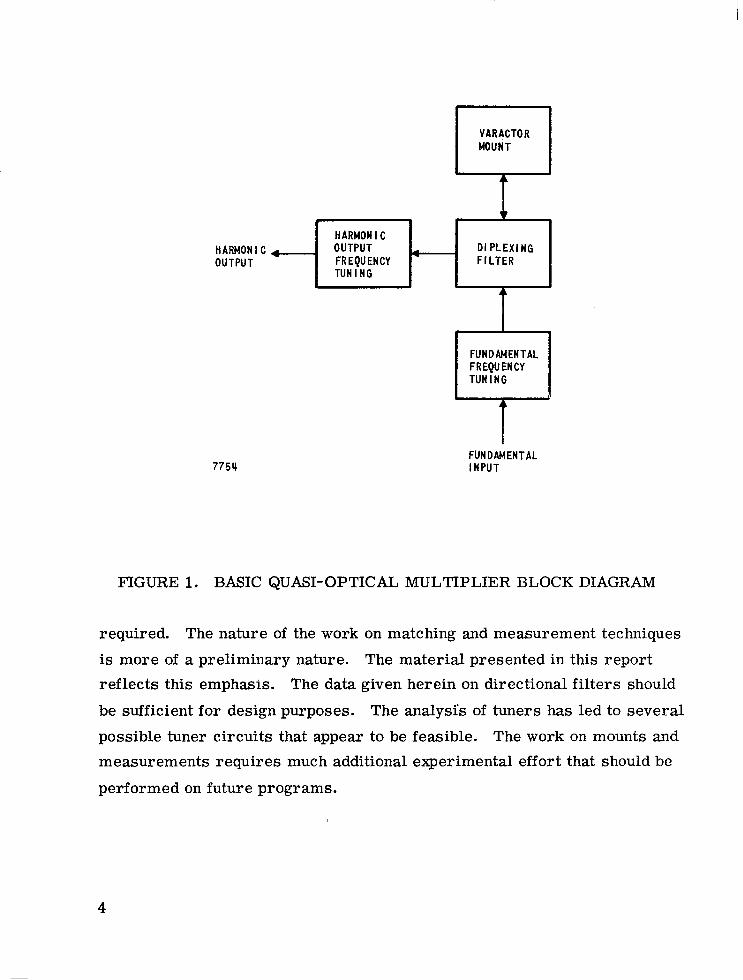
This work serves as a good background because multiplier circuits contain some of these components. For example, a multiplier circuit using quasi-optical techniques would have the block diagram shown in Figure 1.
The diplexing filter function is fulfilled by the directional filter and the va- ractor mount design is aided by the earlier work on focused varistor mounts.
No previous tuner or measurement technique work had been performed.
General Considerations
The nature of the tasks as outlined in the statement of work were such that a detailed theoretical treatment of directional filters and tuners is
3
VARACTOR MOUNT
c ?
HARMON I C HARMON1 C 4 . OUTPUT Dl PLEXI NG OUTPUT FREQUENCY FILTER
TUN I NG
A
FUNDAMENTAL F REQU EN CY TUNING
T 7754
FUNDAMENTAL INPUT
FIGURE 1. BASIC QUASI-OPTICAL MULTIPLIER BLOCK DIAGRAM
required. The nature of the work on matching and measurement techniques
is more of a preliminary nature. The material presented in this report reflects this emphasis. The data given herein on directional filters should
be sufficient for design purposes. The analysis of tuners has led to several
possible tuner circuits that appear to be feasible. The work on mounts and measurements requires much additional experimental effort that should be
performed on future programs.
4

DIRECTIONAL FILTERS
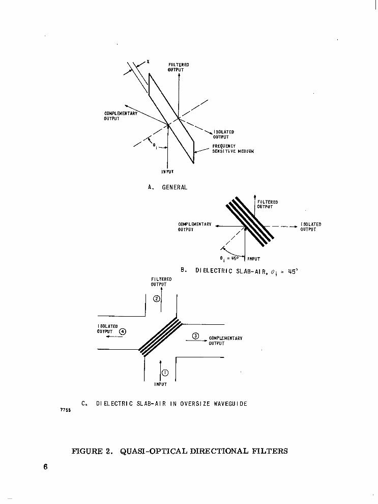
General
Quasi-optical directional filters can be realized by placing a frequency- sensitive transmission path at an angle 0 to the axis of the incident wave; this is shown in Figure 2A. This medium should have an index of refraction n that is a function of x (the distance from the input interface). Such a de- vice can, by properly choosing n(x), be made to have an output with desired passband/stopbands. Power that is not passed is reflected (except for inci- dental dissipation) to the complementary port. A typical characteristic is
shown in Figure 3 . This filter is matched at all frequencies and does not couple to the direction marked "isolated output. ''
In practice, it is easier to realize a varying index of refraction medi-
um in the form of discrete changes created by a series of dielectric slabs
separated by an air region. Furthermore, 8 = 45 is convenient because it places the four ports of interest in a cross arrangement. This circuit is
shown in Figure 2B. Finally, placing this structure in an oversized rec-
tangular waveguide (Figure 2C) yields the structure that is stressed herein.
Reference 9 developed a theory, based on the impedance concept, for
0
analyzing the behavior of directional filters consisting of iterations of dielec-
tr ic slabs separated by air sections of equal electrical length. The starting point in this program was to establish the degree of agreement between theory and experiment attainable over a range of frequencies (encompassing a full passband and a full stopband). The theory is then presented and de- tailed theoretical data is given. These results are used to develop a simple design procedure.
Other designs are also considered
such as the low ripple and modified equal iteration types herein.
5
/ I \
MEDIUM
A. GENERAL
OUTPUT FI LTEREO
t
C t D l ELECTRIC SLAB-AI R I N OVERS1 ZE WAVEGUI DE 7755
FIGURE 2. QUASI-OPTICAL DIRECTIONAL FILTERS
6

1
7766
FIGURE 3. RESPONSE OF A TYPICAL DIRECTIONAL FILTER
Experimental Verification
Partial data on a filter consisting of iterations of four quartz slabs
separated by uniform air spaces was available from reference 9. This showed the inserti.on loss versus frequency from 26 to 40 GHz as indicated in Figure 4A. This filter had a maximum measured insertion loss (port 1-
port 2) of 28 db at 30 GHz and relatively low loss (2 db) at 40 GHz.
To be used in a frequency doubler this filter must have low loss at the second harmonic (60 GHz). Thus, additional measurements were made on
this filter, which are included in Figure 4A. This supplement constitutes insertion loss from 40 - 49 GHz and 56 - 67 GHz. The data indicates that
7

I
lo i i I
I I j ! I
! I
f I
! L E G E N D : 1- THEORETICAL I .L. PORTS 1-2
( & - + - d M E A S U R E D 1.L PORTS 1-2
i * - + - d MEASURED I .L. PORTS 1-3
~
I I
I
d I
20 25 30 35 4 0 4 5 5 0 55 60 65 70
4474 FREQUENCY IN Gtiz
FIGURE 4A. XVSERTION LOSS VS FREQUENCY OF A QUARTZ/AIR FOUR-ITERATION DIRECTIONAL FILTER (g = 1.35gO)
€

w73 FREQUENCY IN GHz
I
# I
I I
FIGUTtF: 4B. INSERTION LOSS VS FREQUENCY OF A QUARTZ/AIR FOUR-ITERATION DIRECTIONAL FILTER (Pl = go)
€
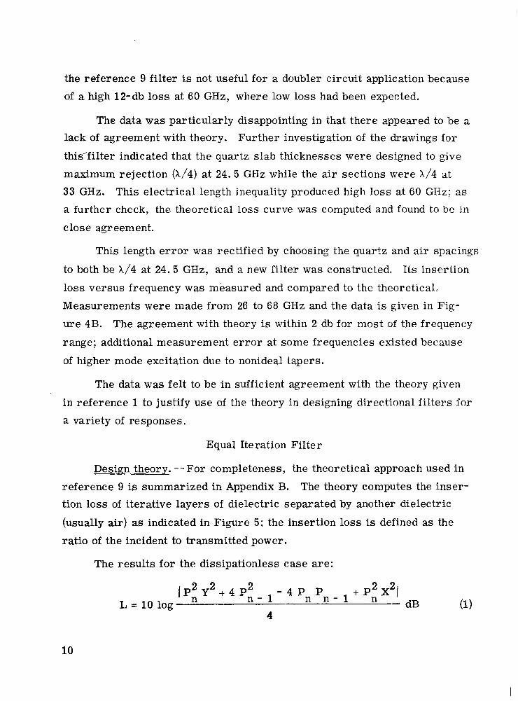
the reference 9 filter is not useful for a doubl.er circuit application because of a high 12-db loss at 60 GHz, where low loss had been expected.
The data was particularly disappointing in that there appeared to be a lack of agreement with theory. Further investigation of the drawings for
this'filter indicated that the quartz slab thicknesses were designed to give
maximum rejection (X/4) at 24.5 GHz while the air sections were X/4 at 33 GHz. This electrical length inequality produced high loss at 60 GHz; as
a further check, the. theoretical loss curve was computed and found to be in
close agreement.
This length error was rectified by choosing the quartz and air spacings
to both be X/4 at 24.5 GHz, and a new filter was constructed. Its insertion
loss versus frequency was measured and compared to the theoretical.
Measurements were made from 26 to 68 GHz and the data is given in Fig- ure 4B. The agreement with theory is within 2 db for most of' the frequency
range; additional measurement error at some frequencies existed because
of higher mode excitation due to nonideal tapers.
The data was felt to be in sufficient agreement with the theory given
in reference 1 to justify use of the theory in designing directional filters for a variety of responses.
Equal Iteration Filter
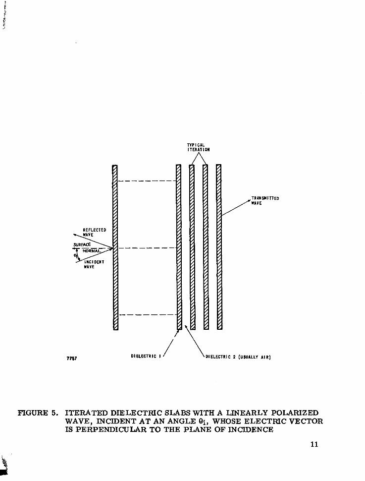
Design theory. --For completeness, the theoretical approach used in reference 9 is summarized in Appendix B. The theory computes the inser- tion loss of iterative layers of dielectric separated by another dielectric
(usually air) as indicated in Figure 5 ; the insertion loss is defined as the
ratio of the incident to transmitted power.
The results for the dissipationless case are:
10
TYPICAL ITERATIOW
""""
""""
""-"
7 n 7 Dl ELECTRIC I DIELECTRIC 2 (USUALLY AIR)
FIGURE 5. ITERATED DIELECTRIC SLABS WITH A LINEARLY POLARIZED
IS PERPENDICULAR TO THE PLANE OF INCIDENCE WAVE, INCIDENT AT AN ANGLE Qi, WHOSE ELECTRIC VECTOR
11
where
n = the number of iterations P = n
Y =
X = pl=
Z =
- -
8. = 1
€ = r
Tchebycheff polynomial of the second kind (equations for Pn are given in Appendix B)
2 cos2 P! - (sin2 ~d) (Z + I/Z) (1/2 sin 2pl) (2 + z + I/Z) electrical path length of each dielectric slab or air separation (defined in Appendix B)*
the wave impedance (normalized to E = 1) of each dielec- tr ic medium r
angle of incidence (between the axis normal to the first slab surface plane and the direction of propagation) relative dielectric constant of each dielectric slab
Substituting the values of Pn from Appendix B gives the insertion loss
as a function of electrical length for specific values of n. The results for
I S n 5 6 are:
For n = 1
l Y 2 + X I & 2 L = 10 log 4
* In this design 'Zlr (the electrical path length in dielectric) and !ifo (the elec- tr ical path length in air) a re equal, that is, 'ZlC = fl = @. 0
1 2

For n = 2
I Y 4 - 4 Y + X Y + 4 1 db 2 2 2 L = 10 log 4
For n = 3
= log I (Y2 - 112 Y2 + 4Y2.: 41Y2 - S Y 2 + (Y2 - 11 x21 db 4
For n = 4
For n = 5
L = 10 log I (.” - 3Y2 + 1)Y2 + 4(Y3 - 2Y)2 - 41.” 4 - 3Y2 + 1) (Y4 - 2Y2)+ [y”- 3Y2 + 11x21 db
(9)
For n = 6
L = 10 log , lY5 - 4Y3 + 3Y12 Y2 + 4lY4 - 3Y2 + 112 - -~ 4(Y5 ~ - 4Y3 + 3Y) (Y5 - 3Y3 + Yl + (Y5 - 4Y3 + 3 Y P x21 db 4
(10)
Examination of these results indicates that L is a function of a, cr , and 8.. For the oversized waveguide directional filters a most convenient choice is ei = 45’. Thus, once €Ii is established, it is possible to compute L versus 1
13

@ with cr as a parameter. Curves or tables of these data can serve as tools in the design of directional filters for a variety of desired responses. It has been found that curves are sufficiently accurate and are more convenient to
use; thus, the design procedures will be based on the use of curves.
Design considerations. --The insertion loss versus normalized fre- quency was computed on a GE time-sharing computer using an advanced
basic programming language. The insertion loss (from port 1 to port 2) L12 versus f(fl) is plotted for 1 through 6 dielectric slabs in Figures 6 - 11.
Assuming, as theory predicts, perfect isolation between ports 1 and 4,
no internal dissipation and no reflections at port 1, the insertion loss at the
complementary output port, that is L13, is obtainable from L12 by virtue of energy conservation: P = P12 + P13 o r Pin = I L13 + L12 I . in
The L12 versus f curves in Figures 6 - 11 are obtained for ei = 45 0
and c r = 2.5; 4.0; 10.0, which correspond to Rexolite (or Polystyrene), quartz, and alumina (or beryllia) relative dielectric constants, respectively.
The abscissae in the above figures were labeled as normalized frequency f ,
which is a linear function of flc = flo = fl; the two are related as fl = Zf. The principal (or the first) insertion loss maximum occurs at f = 1 or fl = - 2 ' Insertion loss is an even function about fl = -and is periodic within intervals
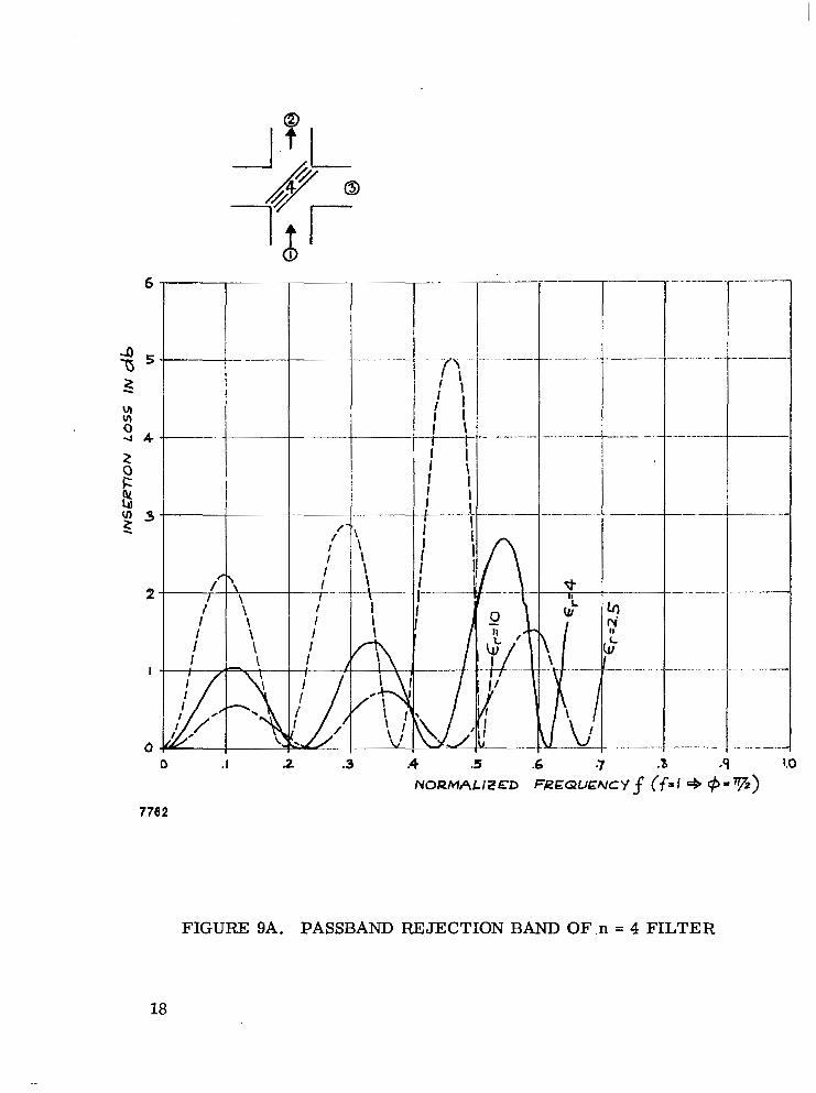
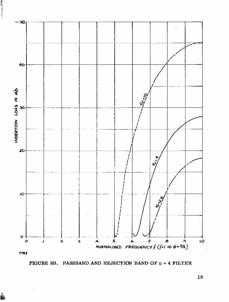
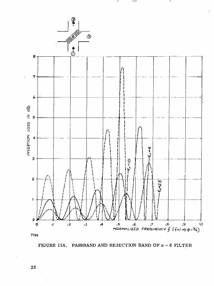
of 71 in fl or 2 in f . The insertion loss peak increases monotonically with increasing cy. For example, if n = 4 and cr = 4 (quartz slabs), the peak
insertion loss is 28 db. Assuming it were used with a varactor connected at port 3, and f = 1 (fl = -) were chosen to coincide with the fundamental fre- quency, virtually all of the power from port 1 will be coupled to port 3.
Second harmonic energy wil l couple from port 3 to port 4 with almost zero
db insertion loss. This is because L and the second harmonic corresponds to f = 2 (fl = rr) which has the same loss a s fl = f = 0.
7
7
IT
2
n 2
34 = L12
14

"-
." -
0 .I .2 .3 A .5 .6 .I?
7761
FIGURE 6. CHARACTERISTICS OF n = 1 FILTER
15

.I .2 ,3 .4 .5 $6 .8 I ,u 0 4
7759
FIGURE 7. PASSBAND AND REJECTION BAND OF n = 2 FILTER
16

c
t V
FIGURE 8 . PASSBAND AND REJECTION BAND OF n = 3 FILTER
17
6
FIGURE 9A. PASSBAND REJECTION BAND 0 F . n = 4 FILTER
1 ! -1-
0 .I .2
776 3
"
I
7!
/i /'
I
.3 .4 .5
/' //
f
e-- -
/"
,/-
-9 LO
FIGURE 9 ~ . PASSBAND AND REJECTION BAND OF n = 4 FILTER
19

I I Q
L
"
-f ""f"
FIGURE 10A. PASSBAND AND REJECTION BAND OF n = 5 FILTER
20

70
20
1 0
0
. ..
..
FIGURE 10B. PASSBAND AND REJECTION BAND OF n = 5 FILTER
21
I I I I" c t---+"--
I
I I I d- l 'L
FIGURE 11A. PASSBAND AND REJECTION BAND OF n = 6 FILTER
22

i
0 .I .2 3 .4 .5 -6 .7 .8 .9 \ .o NoRMALIZ&D FREQUENCYf(f=I => cb-n.>
7767
FIGURE 11B. PASSBAND AND REJECTION BAND OF n = 6 FILTER
23

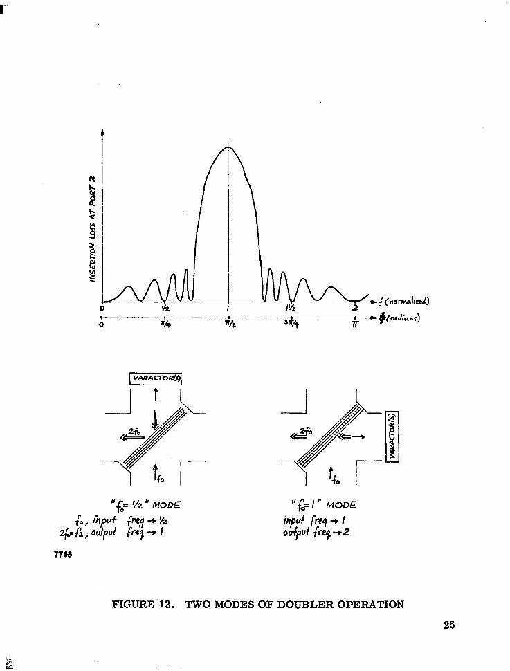
FIGURE 12. TWO MODES OF DOUBLER OPERATION
25

operated in the fo = 1/2 mode, the electrical distances fl ($- and go) equal- 2 radians at the output frequency. In the other mode of open.;ti-ion: "'@ = -:' condition exists for the input frequency, which requires doubling the dielec- tric slab thicknesses and air space separaticns between the slabs. This can
be advantageous at very high frequencies, for a high degree of oversize in the filter waveguide (oversize rztio more than the presently popular I to IO), or when high dielectric-constant materials and few iterations are used.
Otherwise, smaller dimensions a r e usually desirable. In. particular, for those instances where many iterations in the filter are required? ambiguity of the reference plane, as shown in Figure 15, is of necessity introduced; this effect is increasingly proportional to the dielectric slab/& space di-
mensions and may eventually seriously impair the filter perforlxamce.
71
TI 2
Considering single frequency doubling operations and a 1 to 10 over-
size ratio, it is recommended that, at input frequencies below 50 GHz, € =
1 /2 mode of operation be used (varactor located at port 2); at higher input frequencies fo = 1 mode of operation can provide some dimensional advan- tages.
0
If wideband doubling is desired, the f o = 1 mode of operation (cou.pled with the use of a minimum number of iterations and high dielectric constant
materials) offers advantage, but for this application, a different design of directional filter should be employed which distributes and reduces ripple in both pass and rejection bands (see page 46" Low Ripple Filter).
Design procedure. --Once the mode of operation is selected, and the tolerable input/output frequency separation levels (that is, the maximum
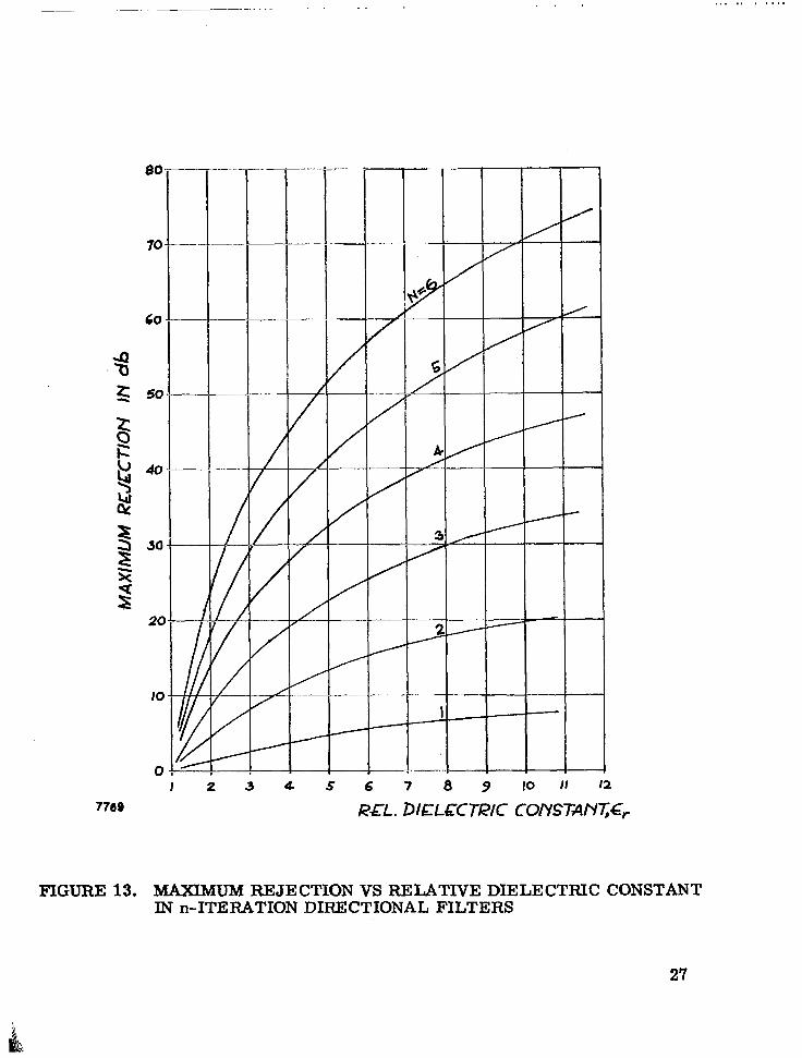
rejection specification) are established, dielectric slab materials can be
selected and the number of iterations determined. Figure 13 shows a disy1a.y of maximum rejection versus dielectric constant for a family of curves representing 1 to 6 iteration cases.
26
"_ ." . . . .. . . . . . .
/ 2 3 4 5 6 7 8 9 l O I i ~ 2 7769 REL. DIELCCTQIC COPISTAN?&
FIGURE 13. MAXIMUM REJECTION VS RELATIVE DIELECTRIC CONSTANT IN n-ITERATION DIRJ3CTIONAL FILTERS
27

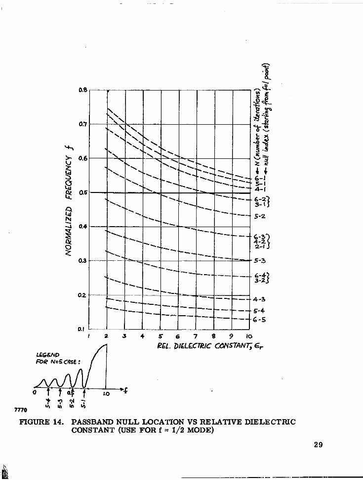
These curves can be applied to the fo = 1 mode case without additional precautions, since at f = 2 there will be a bandpass null regan2less of n or
€ values. For the fo = 1/2 mode of operation, an additional set of con&-
tions is given in Figure 14. It shows how f a r away from f = 0.5 the nearest passband null (at port 2) occurs for a given n and cr. When fo f 0.5 exactly, 2 fo will be shifted from the peak rejection amplitude at f = 1 and hence it will occur at a slightly lower value.
r
Based on the above considerations, a summary of the design proce-
dures of a dielectric/air iterative directional filter for use with a single fre-
quency doubler in a 10-times oversize waveguide system is given below:
Step 1:
Step 2:
Step 3:
Step 4:
Select the mode of operation. Recommended selection: f o = 1/2 mode for input frequencies fo below 50 GHz, fo = 1 mode for fo > 50 GHz.
Establish the desired optimum rejection requirement of the filter; 25 db rejection is recommended as sufficient value for most cases.
a. When operating in f o = 1/2 mode, consult Fig- ure 14 for possible need of "safety factor" in rejection requirement and slight frequency shifts (fo = 0.5 -?A, then 2fo o r f2 = 1 +24) o r additional weighing of n versus c r se l ec - tion advantages. Then select n and F r from Figure 13 data.
b. When operating in fo 7 1 mode, .go directly to
Calculate the filter dimensions: thickness of the air spaces and the dielectric slabs, and &, respectively, using the equations given below:
Figure 13 to select n and €r.
a. For fo = 1/2 mode:
= 20 f X (inches)
fX dc = - (inches)
4 \(E cos (sin -1 1 r
28
Y q S 7770 W U I
FIGURE 14. PASSBAND NULL LOCATION VS RELATIVE DIELECTRIC CONSTANT (USE FOR f = 1/2 MODE)
29

where
Q = relative dielectric constant of the r
f = abscissa value corresponding to the dielectric material
input frequency selection
X = free space wavelength at the input frequency in inches
NOTE
f and X both can be selected at second harmonic frequency--the equation will not change since f (fin) = 1/2f If2) and X (fin) = 2X(fout) , hence
rfXl I = b l c
b. For f = 1 mode: 0
d =- X (inches) O 2 0
X d = € -1 1 (inches)
since f = 1; X here corresponds to the input frequency free space wavelength.
Step 5: Total thickness, DT, of the filter element within the over- sized waveguide junction area will.be given by
DT = ndc + (n - 1) do (inches) (15)
30

An example using these steps is given below:
Desired mode of operation: "fo = 1/2" 2 fo (m rejection desired: minimum of 25 db
Dielectric materials available: quartz, €r = 4 alumina, Er = 9.6
.idband)
or
It can be seen from Figure 13 that four slabs of quartz or three slabs of alumina would suffice to meet the rejection requirements. A look at Fig-
u re 14 shows that for the four quartz-slab filter the passband null closest to fo = 0.5 occurs at fo = 0.43, while for the three alumina-slab filter it is at
= 0.48. Since each has a sufficient safety factor in terms of rejection
at its peak value (28 and 32 db, respectively), slight shifts required of out- put frequencies from f = 1 to f = 0.86 and f = 0.96 will (from Figures 9 and 8, respectively) show the midband rejection at the second harmonic as 25 and
31 db (approximated from cr = 10 curve), respectively. Hence, both con-
figurations are acceptable, with alumina slabs showing advantages in terms of slab thickness and the smaller number of slabs--both factors helpful in reducing the slab fringe ambiguities, which are illustrated in Figure 15 and
are basically self- explanatory; accumulated thickness produces phase-front irregularities in both complementary output ports. Different configurations depicted in Figure 15 will reduce the effects at one output port while aggravating the conditions at the others.
f O
Modified Equal Iteration Filter
General remarks. --Examination of the insertion loss curves for iterative directional filters (flE = Ido) indicates a fair degree of passband ripple activity. These ripples are not theoretically harmful in narrowband (spot frequency) multiplier circuits. However, excessive ripple activity is harmful in practice even in narrowband multipliers because passband cir-
cuit loss becomes an unstable parameter. The filter loss would be overly sensitive to temperatue variations and fabrication tolerances. Wider regions of low passband ripple activity are desirable for wideband multiplier designs.
I
31 +re. ;
"" . - . . . . . . . . , .

777 I
FIGURE 15. ILLUSTRATION OF THE REFERENCE PLANE AMBIGUITY
32
At quasi-optical frequencies, where quarter wavelengths in dielectrics become extremely small, frequency tuning of a directional filter--if bne insists on preserving the 0 = @ condition--may really become very critical.
A study of what happens when the electrical lengths in the air and dielectric sections are not equal (that is, if flo = Kflc) revealed another family of
"irregular filters, " which we call modified iterative filters. These filters a r e not periodic in nm unless K is a whole number. A characteristic of this type of filter, which may be harnessed to good use in the multiplier applica-
tion, is that the passband ripples are irregular and, under certain conditions
wide ranges of frequencies within the passband can become void of any such parasitic ripple. Furthermore, the principal rejection portion of such a directional filter suffers little in peak rejection values; the rejection band- width and the rejection peak are reduced and shifted, respectively, but neither of these three changes renders this type of filter less fit o r objec-
tionable for the use in frequency multipliers. Figures 16A-D and 17A-D
present several curves to illustrate the behavior of this filter, when four and five iterations of air and quartz (E = 4.0) are used in its construction. Unfortunately, we have not found the optimum K conditions for which the peak rejection and the no-ripple-passband regions are harmonically related. Yet this type of filter provides more flexibility in choice of dielectic ma- terial thickness--may allow one to switch from specially ground to less
expensive and easily and quickly obtainable standard thicknesses; or select thicker dielectric slabs for increased mechanical strength where necessary-- o r allows one to readjust o r tune the filter to other operating frequencies
without changing the dielectric slab thicknesses at, most likely, a small change in electrical performance characteristics.
€ 0
r
Design theory. --The filter loss equation, from which the curves of Figures 16A-D and 17A-D have been realized, is of the same form as given
33
I

FIGURE 16A. MODIFIED FOUR QUARTZ/AIR EQUAL ITERATION DIRECTIONAL FILTER CHARACTERISTICS

t
FIGURE 16B. MODIFZED FOUR QUARTZ/AIR EQUAL ITERATION DIRJXTIONAL FILTER CHARACTEFUSTICS

I
. FIGURE 16C. MODIFIED FOUR QUARTAjAIR EQUAL ITERATION DIRECTIONAL FILTER.
CHARACTERISTICS

i
FIGURE 16D. MODIFIED FOUR QUARTZ/AIR EQUAL ITEFUTION DIRECTIONAL FILTER CHARACTEFUSTICS I

0 0.5 1.0 EL EC: LENGTU IN AIR,$ 15 2.0 2! 5
FIGURE 17A. MODIFIED FIVE QUARTZ/AIR EQUAL ITERATION DIRECTIONAL FILTER CHARACTERISTICS

7777

rp 35 - 0
7778
FIGURE 17C. MODIFIED FIVE QUARTZ/AIR EQUAL ITERATION DIRECTIONAL FILTER CHARACTERISTICS

-- I I I I
t 7778
FIGURE 17D. MODIFIED FIVE QUARTZ/AIR EQUAL ITERATION DIRECTIONAL,FILTER CHARACTERISTICS
I

in equation (1) and in Appendix B as equation B - 10, except for a change in expressions of Y and X to negate the assumption do = ffc = ff used in the
equal iteration filter. Therefore, when flo # dc ?
X = 2 sin !do cos d, + z + - sin fl, cos ffo I 'z) Y = 2 COS d, cos fl0 z + - sin ffe sin flo - 1 'z)
and ff, = Kgo
which then must be substituted into the expressions for Tchebycheff poly-
nomials of the second kind, P (equation B-7) and, eventually, insertion loss expression in equations 1 or B-10.
n
Whereas equal iteration directional filter design (6, = ff, case) in- volved only n and B parameters--choosing 8 = 45' as the most acceptable mechanically-- the modified version of it generates an entire family of curves
as functions of K for each Q within a given n. Figures 16A-D and 17A-D
present two families oi" curves (n = 4 and n = 5 at Q = 4.0), to illustrate the trends of K variations and, since c r = 4.0 corresponds to quartz dielectric, all these curves are useful for practical design purposes.
r i
r r
Since the ripple activity in the modified version of the equal iteration filter is not reduced significantly in the region helow the first rejection
peak, fo = 1/2 mode of operation (where L12 is low for f high for 2fin)
should ordinarily not be considered. Hence, a preliminary design criterion for the modified equal iteration filter is that LI2 is high for the input fre- quency, low for the second harmonic.
in'
42
A suggested design procedure is a s follows:
Step 1: Consider available (or desired) dielectric material to tje used in the filter. Establish its relative dielectric con- stant, Cr (keeping in mind that a lower ( r material will re- quire a greater number of iterations, n, to achieve the re- quired results), and its loss characteristics at the highest operating frequency (greater n will aggravate the filter losses).
check the L12 versus ffo curves for that n to see whether the first, or primary rejection peak somewhat exceeds the specified minimum value (usually, 25 db constitute sufficient minimum) for all K parameters under consid- ation. This "safety margin" is required because the filter will operate on the rejection band slope at its input frequency, fin.
Step 2: Select a provisional n value--for the chosen €r-- and
Step 3 : Select a L12 versus ffo curve corresponding to a par- ticular K value and seek out a flat low-loss response region between the primary and the secondary rejection regions. Note the flo value--let us call it a' Look for the L12 value on the same curve at the &2 point. If it is less than the required minimum (25 db), shift, the to the right until 25 db is reached at &/2 o r is no longer in a low-loss region. If the latter occurs first, choose another curve corresponding to a different K value.. If all K's do not provide proper operating points, choose a higher n and start again. When the pl;oper operating points are established, note the final j& and @&/2 values in radians. /
Step 4: Establish the thickness dimensions of the air space'and the dielectric slab, and dc, respectively, using the --.
equations given below: -.. '\
d = - - [ $1 & (inches) 0
and
43

4 Kx -1 1 (inches)
where
X = freespace wavelength at the input frequency in inches [$I = the flo value at the lower operating point in radians
K = the K value for the respective IL versus 12 fl curve 0
E = relative dielectric constant of the dielectric r material
The above two equations could also use @ and X values cor- I c 0'1
responding to the second harmonic, since [ 31 h (fin) = [ 'A] >( (2 fin).
Step 5: Total thickness, DT, of the filter element within the over- sized waveguide junction area will be given by:
D = ndc + (n - 1) do (inches) T
where n = number of iterations
do and d a re as obtained in Step 4. €
An example follows. Given requirements are: L 2 25 db at 30 GHz;
5 1 db at 60 GHz; dielectric material quartz, e r = 4 .0 ; number of iter- 12
L12 ations n not to exceed 5.
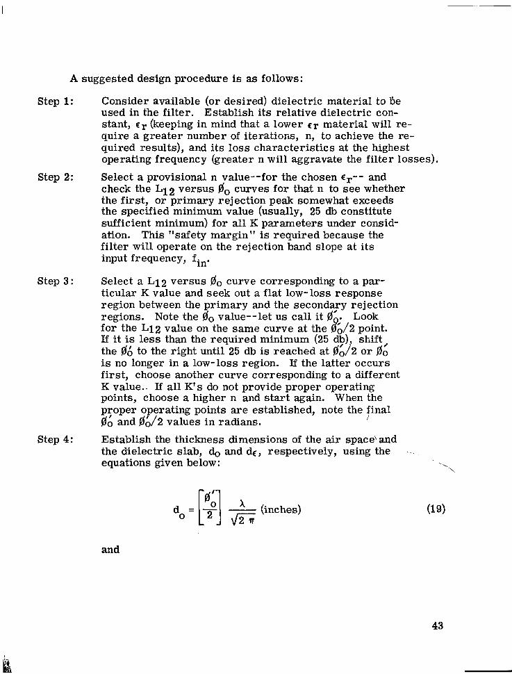
Design procedure starts with selection of the proper family of L12
versus ff curves: = 4; n = 5 a re given in Figure 17A-D. Choosing
K = 1.75 for a f i rs t t ry (it is presented separately in Figure 18 €or clarity), 0
44
4477 .5 1.5 2.0
(RADIANS)
2.5
I'
FIGURE 18. CHARACTEFUSTICS OF MODIFIED FIVE QUARTZ/AIR ITERATION FILTER WHEN K = 1.75

one observes a flat no-loss region at 1.64 < flo < 1 .90 and the principal high- loss region (25 db or better) at 0.90 < flo < 1.32. ' The portions of these two regions which satisfy the requirement of harmonic relationship, that is: fl (at high loss) = 1/2 flo (at low loss), a r e 1 . 8 5 !ifo 5 1 . 9 and 0 . 9 < ld < 0 .95
as indicated in Figure 18. Selecting flo values at the center of each respec-
tive region, fli = 1 .85 radians,-= 0.925 radians to correspond to 60 and
30 GHz, respectively, one obtains do = 0.082" and d = 0.0542" via Step 4
(equations 19 and 20) and the total filter element thickness from equation 21,
0
0
fl6 2
€
DT = (0.054" x 5) + (0.082" x 4) = 0.598" which would be reasonable thickness
in a WR284 waveguide (inside dime.nsions 2.840" x 1.340"). Since the energy at 60 GHz would have to traverse the cumulative thickness of quartz corres- ponding to 5flc = (1.75) (1.85) (5) = 16 .2 radians or 2.58 X, moderate dielec-
tr ic losses within the material of between 0 . 5 and 1 . 0 db are to be expected.
The remarks made for equal iteration (!ifo = ) filter, concerning fringe am- biguities due to excessive filter element thickness as shown in Figure 15, a re applicable in this filter also.
€
Low-Ripple (Stepped Impedance) Filter
Design considerations. --Here we consider the design of quasi-optical
filters formed by cascaded dielectric slabs in terms of its relationship to
modern network theory. The reason for doing this is the promise of lower passband ripple than is achievable with the iterative approaches. Specifi-
cally, these structures are related via the impedance concept for plain wave
propagation to stepped impedance low-pass filters, the synthesis of which has been treated in rigorous detail by Levy (reference 10). He gives tables
for a wide variety of Tchebycheff designs.
In general, there is a tradeoff between pass bandwidth, maximum passband VSWR, number of impedance steps and maximum rejection. Also,
a filter with high maximum rejection will require greater impedance swing at
46

adjacent steps; this will in turn require a wider range of dielectric constants (a narrow range is more desirable--all other things being equal). An ex-
ample of one possible design is given below; it also serves to indicate the steps to be taken in the design of these filters.
Assume that the desired maximum rejection is 20 db and the maximum
passband VSWR is 1.2. From reference 10 we note that N (the number of impedance steps) is 8. Reference 10 gives the normalized (to the generator) impedance of each step; they are listed in the second column of Table I.
These values are then renormalized to the highest impedance value (imped- ance step 5)--this is necessary because the maximum dielectric slab im-
pedance occurs when c = 1. The relative dielectric constant of each step
for the case of normal incidmce is then calculated from: r
where zi is the normalized impedance of the ith step (given in the third column). Values of E a r e given in the fourth column. The last column
gives the dielectric constant for 45 degrees incidence (the directional filter case'); it was calculated from the relationship ~~~o =
ri
Enorm + 1 2
The above filter will yield the results promised by Levy only if the
generator loading is equal to 1/1.78 or 0.562. The normalized load imped- ance should be 0.562 x (maximum VSWR),or 0.562 x 1 . 2 = 0.674.
These conditions cannot be satisfied at all frequency ranges but broad- band X/4 transformers that provide these impedances in the passband of our filter will suffice; mismatched generator and load effects are less critical
in the rejection band.
47

TABLE I
Step No.
1 2 3 4 5 6
7 8
LOW-RIPPLE FILTER IMPEEANCE AND DIELECTRIC CONSTANT STEPS
Normalized Impedance
1.33 0.78 1.70 0.675 1.78 0.705
1.54 0.902
Impedances Normalized
to Ster, 5
Relative Dielectric Constant for a
Normal Incidence Filter
Relative Dielectric Constant for a 4 5 Incidence
Filter
0.745
0.438 0.95 0.3 78 1.0 0.394 0.865 0.506
1.8
5.2 1.1 7.0 1.0 6.4
1.34 3.9
1.4
3.1 1.05 4.0 1.0 3.7 1.17 2.45
A two-section 1/4 transformer on each end will suffice. From Young (reference l l ) , the generator side (a VSWR of 1.78 exists if not matched) over a 3 to 1 band will be within a maximum VSWR of 1 .21 and this requires X/4 sections have Z1 = 0.678 and Z = 0.828. These impedances are nor- malized to that of free space
2
The load side will match a 1.49 VSWR to 1 .22 over a 4 to 1 band and requires Z = 0.777 and Z2 = 0.864. The X/4 transformer impedance data is then converted to dielectric constants as shown below.
1
Genzator Side Load Side I
- ...-. " - __
2 value norm €45O ' Z value " 'norm 'Z €
z1
z2
0.678 2 .12 1.56 0 .777 1 .65 1.33
0.828 1.46 1.23 0.864 1.33 1.16
Figure 19 shows the structure, the dielectric constants, and the thick- nesses of the dielectric slabs.
The thickness (tc) values were calculated from
For the eight filter sections fl = n /2 at the maximum rejection wave- length XR. We shall place the design center of the X/4 transformers at fl = 71
when X = X Thus, we have R'
49

7780
"- - - "" J
I I I I
r--------- """"
I I 1 1
FIGURE 19. LOW RIPPLE FILTER DESIGN PARAMETERS
50

for the filter sections and
for the transformer sections.
These data together with the design of two section transformers using Young's tables complete this theoretical design.
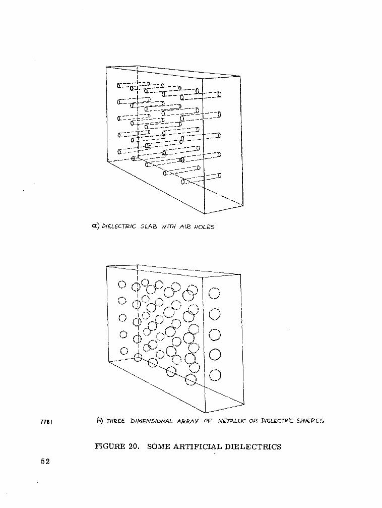
The next step is one of realizing in practice that dielectric constants required. Since most of these values do not exist in low-loss natural dielec- tr ics, it requires the use of artificial dielectrics. This topic is considered next.
Artificial dielectrics. --The realization of the low passband-ripple directional filter described in the previous report requires the availability
of materials whose dielectric constants range between c0 and 46 0'
Many of the values required are not available in their natural state. While certain foam (Eccofoam) and ceramic (Ray K) dielectrics are available in a wide range of values, the former is limited to low (2 or less) relative dielectric constant values and the latter's loss properties at millimeter wavelengths a r e poor. Two approaches are described herein: (1) a three-
dimensional a r ray of spherical conductors or dielectrics, and (2) a two-di- mensional a r ray of holes in a dielectric slab. These offer the possibility of obtaining a wide variety of dielectric constants with low dielectric loss tan- gents. Both types are shown in Figure 20. The second approach is pre- ferred but more design information is required.
Array . of metallic or dielectric spheres. --The effective relative di-
electric constant and permeabilities of metallic and dielectric spheres that
51
778 I
52
FIGURE 20. SOME ARTIFICIAL DIELECTRICS

are embedded (in a regular three dimensional pattern) in a supporting di-
electric medium, have been derived in reference 12. The results are
and u = u1 for dielectric spheres eff
'eff = '1 0- - f ' for metallic spheres
where
f = ratio of sphere volume to total volume, or filling factor
1 E = relative dielectric constant of the surrounding medium
E - € S
S C = for dielectric spheres, = 1 for metal spheres E + 2 E
e = relative dielectric constant of the spheres S
In our application it is easier to use the dielectric sphere case because we prefer to avoid variation in permeability. Figure 21 shows curves of E /Q as a function of f with Q / € as a parameter. These curves are useful in determining the sphere filling factor required to achieve a given dielectric constant. They also apply to the metallic sphere case (E - For example, if E = 2 . 3 is desired for a case where all spheres use air
(cs = 1) as the dielectric and the base dielectric is Rexolite (E = 2.55) one
has 'eff €1 specific sphere diameters should be chosen such that there is a center-to- center spacing, s, much less than a free space wavelength. Thus, at X =
1 cm (30 GHz) spacings of 0.1 cm would be desirable. The filling factor is
related to sphere spacing s and the sphere radius a by
eff 1 s 1
S >. eff
1 / = 0.902 and E /E = 0.555; a value of f = 0.19 is required. The s 1
53

0. I 0.2
7782
0.3
I I
0.4 0.5
I
FILLING FACTOR f
FIGURE 21. DIELECTRIC CHANGE FACTOR VS FILLING FACTOR
54
3 4 n a 3s
f =3
Substituting the above values of f and s gives a = 0.036 cm. In like fashion other dielectric constant values can.be achieved.
Array .. . . of holes in a dielectric medium. --The presence of an array of , - -
holes (dielectric constant eo) in a medium of relative dielectric constant C3/cO results in an effective relative dielectric constant that is less than c3/CO but greater than unity. No exact formulas exist but approximate for- mulas have been used in the design of quarter-wave transformers for sur-
face matching. Reference 13 gives a formula for the ratio of hole a rea to total surface area (Rhole) required to match dielectrics and €l, to each other. It is
where p = ( ~ t ’ ~ s in Q1], and 0 is the angle of incidence. In our case E = 1
(air holes) and €I1 = 45 , hence 1 1
0
1 /2
P + €3) (3 € - 1/2 - [jZ3 - $1 4 ) 2rg (E3 - 1) (3 0) Rhole
- _ _ _ _ _ ~ ~ ~ -
The matching section is equivalent to a relative dielectric constant
55
Thus, for example, air holes drilled in quartz (Er = 4) according to the above, would produce an artificial dielectric with Q = 2.37. For other
val’ues one can experimentally determine the variation of Q with hole area. We also expect to develop a theoretical expression for hole area applicable to any desired Q value. In any event, the use of artificial dielectrics,
whether the design data are theoretically o r experimentally determined,
offers a practical method of obtaining the dielectric constant values required for fabricating low passband-ripple directional filters.
2
2
2
56
TUNERS
Adjustable impedance transformers or tuners are required in order that multiplier circuits present the desired generator and 1oa.d impedances to the varactor. Considered herein are three basic types of quasi-optical waveguide tuners.
Type 1: The tuner consists of two equal fixed value susceptance gratings whose separation and distance from the load to be matched are variable; this tuner is illustrated in Figure 22. Type 2: This tuner consists of two variable susceptance gratings that are located at fixed positions; Figure 23 shows one possible design. The variable susceptance is achieved by using slot- type apertures in each grating. Rotation of the grating produces a continuous range of susceptance values between the minimum value (slot axis perpendicular to the polarization direction) and the maximum (slot axis parallel to the polarization direction). Type 3: A variable susceptance grating whose distance from the load is movable constitutes this tuner; it is the quasi- optical equivalent of a slide screw tuner. Figure 24 shows one possible embodiment. The variable susceptance is achieved by moving one plate relative to the other; the effective aperture a reas are varied by prescribed misalignment of identical aper- tures within each metallic plate, thereby changing the sus- ceptance value a t that transverse plane. In addition, this variable susceptance plane can be moved along the longitudinal axis of the waveguide.
To assess the electrical properties of each type, the analysis of the conditions required for matching arbitrary loads and the resultant tuner dis-
sipation losses are presented. In these analyses, the assumption is made that the oversized waveguide dissipation contribution is negligible com- pared to that of the susceptance gratings.
57
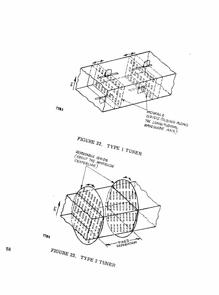
58
7784

PLATE 12 PLATE % I
7706
J APERTURE S 1 ZE CONTROLLED BY DISPLACWENT OF PLATE Y2 WITH RESPECT TO PLATE # I
FIGURE 24. POSSIBLE TYPE 3 TUNER CONFIGURATION
Type 1 Tuner
Matching conditions. --By moving the position of plane aa relative to bb (variation of QL) in Figure 25, it is possible to present a load reflection
coefficient of magnitude I rLI and of arbitrary phase @. We have matched the load when raa = I rL I e-]@; is defined as the reflection coefficient looking to the left of aa. Since @ is arbitrary, the only new condition to be
raa
set is lraal = IrLl. The value of Taa is obtained from transmission line theory:
2 - j(b s in 8 - 2b cos 8) raa - ~ - . . . _ _ . ... . . . . . ~ - . ..
(2 cos 8 - 2b s in 0 ) - j (2 s in 8 - b2 sin 8 + 2b cos 8)
59

7786 a
FIGURE 25. EQUIVALENT CIRCUIT OF A TYPE 9 T U N E 3
2 2 Letting I l?L I = a, the matching condition is I l',, I = a o r
1
l + 4 4"
2 4 2 3 b + (4b - b ) cos 8 - 2b sin 20
where
b = normalized tuner susceptances 8 = separation between the two susceptances
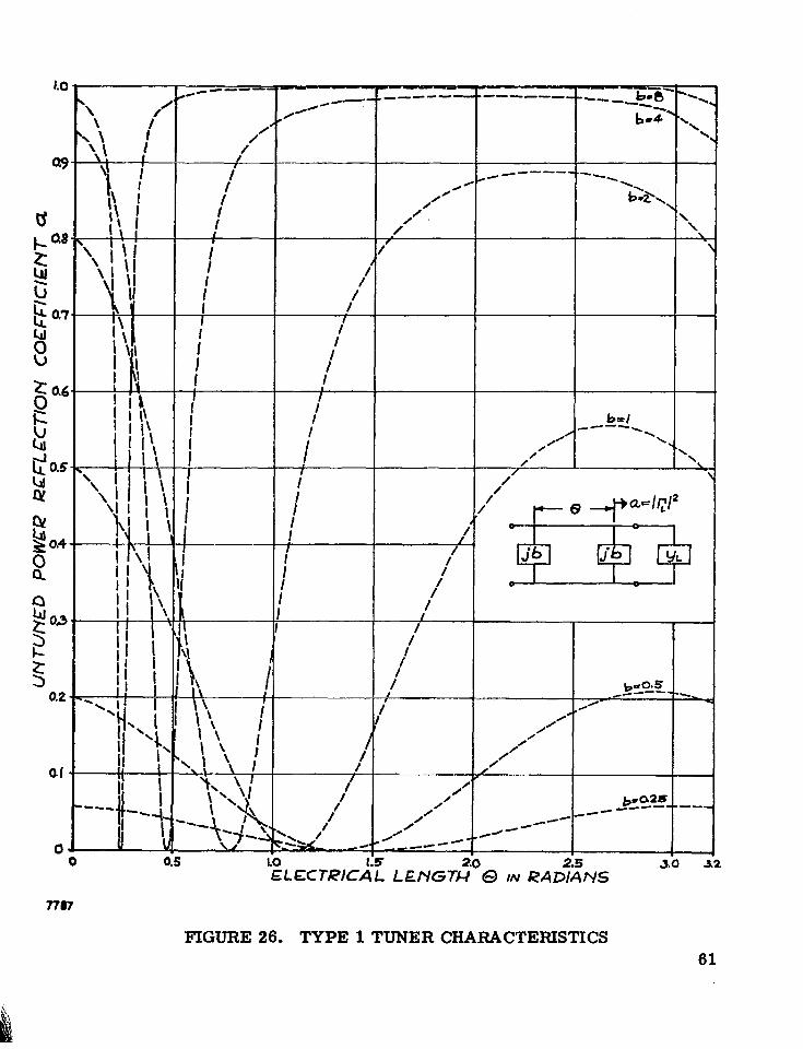
A plot of a vs 8 with two equal normalized susceptance values b as a
parameter is shown in Figure 26; values of b of 0.50 cannot match any values of a greater than 0.21. Large b values give a greater range of matching
effectiveness but the separation becomes critical when small values of a must
60
" C "" bra2s __. t
7787
FIGURE 26. TYPE 1 TUNER CHARACTERISTICS 61
be matched, a s evidenced by the sharp notch in the high b curves. A choice of b = 2 appears to be a good compromise; it can tune out loads with a values
from 0 to 0.88 (1 to 32 VSWR) and i ts low VSWR notch is not overly critical.
Dissipation - .- - - -. " . - loss. - - " --.The first step in the analysis of dissipation loss for the type 1 tuner is to obtain a suitable model; this mode1 is related to the type
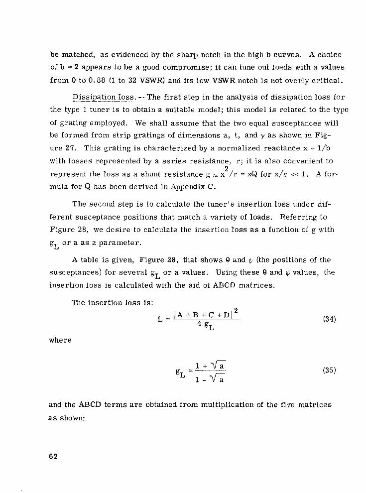
of grating employed. We shall assume that the two equal susceptances will be formed from strip gratings of dimensions a, t, and y as shown in Fig-
ure 27. This grating is characterized by a normalized reactance x = l /b
with losses represented by a series resistance, r; i t is also convenient to
represent the loss as a shunt resistance g x /r = x& €or x/r 1. A for- mula for Q has been derived i n Appendix C.
2
The second step is to calculate the tuner's insertion loss under ciif-
ferent susceptance positions that match a variety of loads. Referring to Figure 28, we desire to calculate the insertion loss as a function of g with
g o r a a s a parameter. L
A table is given, Figure 28, that shows 0 and $ (the positions of the
susceptances) for several gL or a values. Using these 8 and I$ values, the
insertion loss is calculated with the aid of ABCD matrices.
The insertion loss is: 0
I A + B + C + D [ z L =
gL where
(3 4)
and the ABCD terms are obtained from multiplication of the five matrices
as shown:
62
9 ) S TRIP GRATING (TWO VIEWS)
7780 b) IVORMALIZED EQUIVALENT CIRCUITS
F'IGURE 27. GRATING REPRESENTATION
63

2+ ,'/'
13.28" 0.80
573' 50.90 0.27
i t I
18.05
3.15
1
0 0 0. I 0.2 0.3
LOSS CONDUCTANCE (9) 7789
FIGURE 28. DISSIPATION OF A MOVABLE SUSCEPTANCE (TYPE 1) TUNER VS INCIDENTAL SHUNT CONDUCTANCE WITH gL AS A PARAMETER
64

The insertion loss vs gL for various g values (and their corresponding 8 and # values) was obtained with the aid of a digital computer and is shown in Figure 28.
The values of g for a metallic strip grating can be determined from Q formulas given in Appendix C. Examination of Figure 28 shows that g = 0.1 results in a tuner dissipation loss of 2.3 db or less ; the g for the copper
grating operating at 30 GHz (described in the Appendix C) is 1.33 X
Its loss can be accurately determined by interpolation. Thus, an upper
bound for the tuner loss is
These results indicate that dissipation loss should be negligible in the
example chosen. The loss increases only as the square root of frequency,
hence these conclusions are probably accurate up to 300 GHz, where the estimated tuner loss is 0 .1 db.
Type 2 Tuner
Matching conditions. --The ability of this device to match a wide range of impedances is a function of the separation between the variable susceptances. An equivalent circuit of this tuner is given in Figure 29 and the analysis for the
case of 3/8X separation is given in Appendix D. Other separations (x/4 and >/2) have also been considered but they are more limited. Thus, only the
best case is presented. The analysis shows that any conductance equal to or
65

less than 2 and any value of susceptance can be matched. For any reasonably high Q varactor, the conductance should be considerably less than 2. It thus appears that this type of matching is theoretically adequate. Practical limits on the range of susceptance will further restrict the matching range.
Dissipation loss. --With the aid of Appendix D one obtains for the loss-
less 3/8x separation case:
bl = -1 - + d m
where g + jb represents the admittance to be matched and b b2 are the two
tuner susceptances. For simplicity, assuming b = 0 and considering only 1'
the bl = -1 + 7./ (2/g) - 1 case, which consequently results i n b2 = -1 + g
q m representing the "matching" condition, let us introduce tuner
losses. The equivalent circuit is shown in Figure 30. The tuner grating losses are designated as CY I bl I and CY 1 b2 I , where CY is closely related to a reciprocal of grating Q factor, that is gi I bi I /Qui. This relation, we
believe, could be reasonably assumed to be true within a small multiplying factor (of 2 o r 3) from the point of grating current considerations for high
and low susceptance limits. The equivalent circuit in Figure 30 is accom- panied by the element ABCD matrices and the insertion loss equation. The
results are plotted in Figure 31 in terms of tuner insertion loss (both grat- ings included) vs r, the normalized load resistance (r = l/g). The range of
10 < r < 100 should include the practical application values for low-loss
varactor loads. Referring to Appendix Cy where Q's of strip gratings are analyzed, the practical Q values are estimated at about 1500, hence the expected tuner losses should be at or below 0 .2 db in a given practical varactor multiplier application.
66

FIGURE 29. EQUIVALENT CIRCbTT OF A LOSSLESS TYPE 2 TUNER
779 I
B D
FIGURF: 30. LOSSY TYPE 2 TUNER REPRESENTATION
67

/-" +- ""C _____
" I
0 20 40 60 80 IOU
NORMALIZED LOAD RESISTANCE, r 7792
FIGURE 31. TYPE 2 TUNER LOSSES
68

Type 3 Tuner
Matching conditions. --The schematic for analysis purposes is an exact
equivalent of a slide-screw tuner within a regular waveguide as shown in Fig- ure 32. The complex load admittance yL, to simplify the analysis, is viewed from a plane at some distance toward the generator where it can be repre- sented as a conductance g In other words, representing this operation on the Smith Chart, we have added a segment of transmission line in front of the load yL necessary to rotate it along the constant VSWR line into the con- stant resistance (or conductance) axis. Furthermore, to facilitate the use of the ABCD matrix in the analysis, the load conductance is represented as
shown in Figure 32B. From the ABCD matrix:
L'
A B COS 8 jsinQ
(c D ) = ( ,fb y ) ( jsin8 cos 0) ((g: - 1) :) the input admittance at a plane immediately in front of the tuner susceptance sheet, looking toward the load is:
The matching conditions then are obtained equating gin = 1 and bin = 0 and
reducing the resultant expressions of the position and susceptance param-
eters in terms of the load conductance as given below:
69

I” I tuner I
I
I
1 I
7793
F’IGURE 32. TYPE 3 TUNER
70
where 1 is equal to the distance between the susceptance plane and the refer- ence plane where the complex load appears as a pure conductance.
The above expressions are valid for all values of gL, greater or smaller than unity (9, = 1 being a trivial case). The susceptance spread required to tune out the load mismatches can be seen in Figure 33 where
I b I vs VSWR is shown (+b is required when VSWR value corresponds to -b when VSWR corresponds to rL = l/g ). Distance L (defined pre-
viously) varies between 0. l A g and 0. OIAg when 200 < gL < 2; for 200 < r L < 2 parameter L varies between 0. 15xg and 0. 24Xg. Considering the maximum additional (slightly less than 0 . 2 5 ~ ~ ) length that may be required to transform the complex admittance into a pure real (conductance) value, the desirable travel distance of the variable susceptance plate would approach a half wave- length, i f the maximum possible tuning range is desired.
gL' L
Dissipation. --The losses are introduced for the susceptance plate only
in the form of a shunt conductance, which--as in the previous two types of tuners--can be assumed to be directly proportional to the magnitude of the susceptance and inversely to the unloaded Q of the susceptance plate, that is,
g I b I /Q . The new schematic, shown in Figure 32C, will have the element
jb changed to g + jb. The insertion loss is obtainable from U
/ A + B + C + D l 2 L = 10 log
4gL (44)
with the previously determined matching conditions applied. This results i n
2 L = 10 log (1 ' 5 ) (45)
71
14
12 '
IO
$ 1 a
IO 20 VSWR
" . ...
1 1 i
x) IO0 200
FIGURE 33. NORMALIZED SUSCEPTANCE OF TYPE 3 TUNER VS VSCVR
72

but since
the final expression becomes:
The insertion loss versus VSWR(befo.re tuning), is shown in Figure 34 for Q = 10, 100, and 1000. Due to the absolute value term in the insertion loss
expression, VSWR in this case corresponds directly to gL or r magnitude. Here again, for susceptance Q' s in excess of 1000, the tuner loss is small;
it is under 0.1 db.
U
L
Comparison of Tuner Types
The analyses of the three types of tuners indicate that type 2 has a limited range of .impedances that it can tune and is therefore least desirable.
Types 1 and 3 are not s o limited. All tuner types have low dissipation loss (less than 0 . 2 db). The preferred tuner is type 3 because it is the one most
likely to produce a broader band match; this is because tuning can be placed closer to the varactor mount than is possible with the type 1 tuner. The subsequent discussion of practical tuner realizations will stress the type 3
tuner.
73

/ 2 5 10 20
77ac vswu (BEFORE TUNING)
100 200
FIGURE 34. TYPE 3 TUNER INSERTION LOSS vs VSWR v . 7 1 ~ ~ TUNER PLATE Qu AS A PARAMETER
74
I

Mechanical Design Considerations (Type 3 Tuner)
The mechanical design of the type 3 tuner is essentially that of realizing
a susceptance that is variable in value and position along an oversized wave- guide. One possible design is shown in a cross section side view in Fig- u re 35.
The variable susceptance consists of two thin dielectric (probably quartz) slabs. One surface side of each dielectric slab contains a deposited metal grid-work containing a pattern of evenly spaced square (or rectangular)
holes within a metallic sheet, as shown in Figure 36, o r horizontal and vertical metallic lines. Both slabs have identical grid patterns and, when assembled the metallic sides will face each other, but will not contact each other or
FIGURE 35. SIDE VIEW OF TYPE 3 TUNER
75

SLAB " A " (STATIONARY) SLAB "B- (MOVABLE VERTICALLY)
MAXIMUM HOLE S IZE POSIT ION
SUSCEPTAIICE) ( M I I I M L M
SLAB "A " \
S I Z E P O S I T I O N
SUSCEPTANCE) (MAXIMUM
NOTE: EFFECTIVE RECTANGULAR HOLE
7797 SLABS, ARE SHOWN I N BLACK AREAS, PRODUCE0 BY TWO OVERLAPPING
FIGURE 36. SUSCEPTANCE VARIATION PRINCIPLE
One of the two dielectric slabs, marked A on Figure 36, would be sta-
tionary, and the other would move in the vertical direction. This resu.Its in
changing geometrical configurations of the rectangular grid holes from square
to rectangular slits, as illustrated in Figure 36, thereby changing the EUS-
ceptance value of the combined susceptance plate.
The mechanical means of susceptance variation within the plate and the
longitudinal motion of the combiced plate and its guiding structure within the waveguide are illustrated in Figure 37. The slits on the top and the bottom
waveguide walls are located at electrically inert surface areas (where the
76

electromagnetic currents are pa rd le l to the slit), and the gear mechanism is to keep the susceptance plate perpendicular to the longitudinal waveguide axis at all times to reduce the possibility of generation of higher order modes within the waveguide.
Additional Tuner Design Problems
The practical design of tuners with moving and variable susceptances produces some effects which are considered herein.
Moving susceptance effects. --Tuner designs requiring moving sus- ceptances (including types 1 and 3) can be designed with sliding contacts or without any contacts. The sliding contact approach implies the use of spring
fingers which ultimately create intermittent difficulties. Thus, we prefer the noncontacting approach provided its effect can be tolerated. The effect of no contacts on the susceptance of a tuner plate is considered below.
VERTICAL MOTION CONTROL /(FOR PLATE "E")
ONGITUDINAL MOTION CONTROL FOR THE WHOLE SlR UCTURE)
INSULATION LAYER
PLATE ' 'A" AND THE W l D l N Q STRUCTURE
WR 289 WAVEQUIDE MECHWlSn (FOR PLATE "6")
7798 FIGURE 37. FACE VIEW OF TYPE 3 TUNER
77

Let us assume that a tuner susceptance is removed from the four wave- guide walls by an air gap of width d as shown in Figure 38. The air gap will add four reactances in series with the desired reactance X The sum of the horizontal gap reactances ( X J is given in Marcuvitz (reference 14). By using the relations for a capacitive obstacle with d << b one obtains
P'
Xh'" - l g 2b t n ($)
Similarly for X one uses the relation for inductive obstacles with d << a. V
This yields
4 (49)
For the oversize waveguide size of current interest a = 2.84" and b =
1.42 "; the gap d may be as large as 0.003f'. For these values one obtains at 30 GHz (X = 0.39"), xfl = 1.1 x IO-'' and Xv = 1.33 x The sum of these two values is essentially X
g V'
The X value is a factor only in so far as it adds to the desired reactance. V
When tuning out low VSWR's the desired reactance will generally be at least
100 times greater than X and is therefore negligible. For large VSWR's X
may have to be as low as 0.1, in which case Xv has a 13 percent effect. While not negligible, it does not limit the ability of the device to tune out large VSWR's.
V P
In summary, a noncontacting susceptance will behave satisfactorily and is, therefore, the preferred approach.
78
7799
- normolized +&I horizo,ztu/ gap reactance
)(,=narmalized t o ~ l ver+Lol gap reactance
FIGURE 38. NONCONTACTING TUNER PLATE REPRESENTATION
79
Effect of a dielectric substrate on tuner performance. --It may be
necessary to form the susceptance on a dielectric substrate. A susceptance formed by etching a metal surface that was vacuum deposited on a dielectric (such as quartz) substrate (Figure 39) will be a function of the dielectric constant and its thickness. This can be represented by its composite ABCD matrix.
- j Z sin gc
E
where
t = Dielectric thickness Z = l/F, the normalized impedance
€ r
The net ABCD values are
A = cos gc, B = j Z s in Idc E
D = COS gs - bZc sin (IE
In one design, the thickness can be chosen such that $ = n and 2n at the €
fundamental and second harmonic respectively. For this case:
80
7800
FIG= 39. SUSCEPTANCE FORMED ON A SUBSTRATE
This would be equivalent to a pure shunt susceptance at the frequencies of in-
terest and the tuner would therefore be unaffected by the presence of the
dielectric.
In another case one may have an electrically thin (@ << 1) dielectric. €
The ABCD values become:
81
t

The voltage transfer coefficient is:
2 2 T = -
A + B + C + D - 2 - b Z c ! i f E + j [ b + g C ( Z € + 1 / Z ) ] E
Examination of T shows that for:
2 T = ____le - 1 2 + ! i f z z (Z + 1/ZJ
€ € E
(5 3)
(54)
(55)
and for b+m, T+O.
Values of T between 0 and 1 are obtained for intermediate values of b. Since the network is lossless, the magnitude of the reflection coefficient is
Thus 1 rl can be set to any value between 0 and 1 by varying b and the effect of the substrate is therefore not serious.
Concluding Remarks
The theoretical investigation of tuners indicates that the type 3 tuner is
the most desirable. A preliminary mechanical design appears to be feasible, It is believed that the next step is the construction and evaluation of the type 3
tuner. This work will be undertaken on a future NASA ERC contract.
82

VARACTOR MOUNTING TECHNIQUES AiW REPRESENTATION
General Remarks
A varactor or a group of varactors constitute the most important part of a varactor frequency multiplier; selection of a suitable varactor and imbed- ding (mounting) it properly within the circuit determines the multiplier effi- ciency and mode of operation. Presently, the varactor mounting techniques and their equivalent circuit representations are little-explored areas in the quasi-optical frequency multiplier component design field.
Several years ago, when only the encapsulated varactors in a pill o r so- called double-ended package were commercially available, the problems they caused at high frequencies (starting at K-band) were stemming from parasitic package inductances o r stray capacitance and the comparatively low self- resonance frequencies. With the recent introduction of the beam-lead varac- t o r s (and varistors as well) into the market the parasitic susceptance effects become less prominent. The efficiencies of such varactors at multimeter wavelength are improved by quite a margin. The problem still present in the multiplier circuit design concerns efficient varactor mounting techniques-- proper impedance matching, lossless connections, and reduced parasitic SUS-
ceptance elements in the mount,
Most of the results of varactor multiplier design theory developed for multiplier circuits in the conventional single-mode transmission line, like
input/output impedance tuning, power handling, and efficiency predictions, are most likely applicable to quasi-optical varactor multiplier circuits with- out major modifications. Yet now the varactor imbedding circuits must be developed to reflect the oversize waveguide propagation techniques--proper interception of the energy propagating in the oversize waveguide, minimum possibility of excitation of higher order modes, crosspolarization of fields in the waveguide, etc.
83

After a careful consideration of various factors, advantages, practical realizability and limitations, the acceptable basic varactor mounting configu- rations have been reduced to three:
1. Focused varactor mount (single varactors) 2 . Large varactor array mount 3 . Partially focused small varactor array mount
These three basic mounts are shown in Figure 40 and discussed below.
Varactor Mounting Techniques
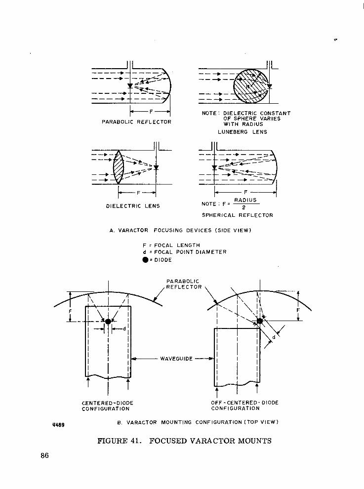
Focused varactor mounts. --This varactor mount consists of a single varactor situated within o r without the oversized waveguide area and a focus-
ing device (lens or reflector), as shown in Figure 41.
The energy focusing devices, such as dielectric lenses or conducting metal reflectors, have an inherent imperfection, o r so-called circle of con-
fusion, at their focal point at finite incident wavelengths. The diameter d of this circle of confusion (or "focal point diameter") can be expressed in t e rms of the focal length of the device F, incident wavelength A , and aperture dimen- sion D (diameter of a circular antenna aperture or side length of a square an-
tenna aperture) in this manner.
F X k D
d =-
The constant k usually assumes values 0.89 " < k < 1 . 5 depending on the illuminated aperture edge contour shape and the incident power distribution.
Actually, the circle of confusion is part of a fringe pattern of the power
reflected by the antenna at its focal plane, shown in Figure 42. The circle of confusion diameter is defined as the distance between half-power points
(3 db below peak reflected power) of the main lobe. From the equation, it
84

TOP VIEW \
"
- --- TPARA"" -+%- ""_ F
PARABOLIC REFLECTOR
4 , S I N G L E D I O D E FOCUSSING
WAVEGU I DE
+ + + "". . . . . . T T T + + . . . . . . . . .
. . VARACTOR . .
. . . . . MATR I X . . . . . . . . . . . . . . .
VARACTORS' \SUPPORTIMG
HATER1 AL
B . VARACTOR ARRAY
SIDE VIEW
"-
FRONT VI EW
7801 C. P A R T I A ' L FOCUSI.NG
mGURE 40. VARACTOR MOUNTING TECHNIQUES
85
I I I III
NOTE: D IELECTRIC CONSTANT
PARABOLIC REFLECTOR OF SPHERE VARIES W I T H R A D I U S
LUNEBERG LENS
t-F"--l
D I E L E C T R I C L E N S R A D I U S
2 NOTE : F =
S P H E R I C A L R E F L E C T O R
A. VARACTOR FOCUSING DEVICES (S IDE V IEW)
F = F O C A L L E N G T H d = F O C A L P O I N T D I A M E T E R
= DIODE
CENTERED-DIODE CONFIGURATION
O F F - CENTERED - DIODE C O N F I G U R A T I O N
Pv89 8 . V A R A C T O R M O U N T I N G C O N F I G U R A T I O N ( T O P V I E W )
FIGURE 41. FOCUSED VARACTOR MOUNTS
86

(NORMALIZED) POWER
. FIGURE 42. FRINGE PATTERN AT FOCAL PLANE
is evident that the circle of confusion would be negligible (that is, ideal point- focus solution of geometric optics applies), if the illuminated aperture is very large, as in a case of antenna dishes, o r the wavelength is very small (for example, visible light spectrum). In our case neither is true. The energy density in an oversize waveguide is not evenly distributed as in a .plane wave case over the cross-sectional area of the waveguide, but rather resembles TEIO mode distribution (that is, peak density at the center, re- ceding sinusoidally toward the sidewalls). At 33 GHz, h = 0.358 inch in
WR 284 waveguide, which is 10 times oversize D = 2 . 1 inches (average of 2.840 inches and 1.420 inches). Using F = 2-inch parabolic reflector, the circle of confusion has a diameter d = 0.35 inch. Some input energy would therefore be lost due to phasing differences at the varactor located at the focal point, but the efficiency of a varactor multiplier should not suffer excessively at this point.
87

Another problem which remains is to launch a wave at the harmonic
frequency via the focusing device back into the waveguide. This needs ex- perimentation, since by applying theory alone (which could not possibly contain a rigid solution), prediction could be excessively far from practical truth.
Varactor array. --Another way of mounting a number of varactors in an oversized waveguide is to connect them in a prearrmged pattern within a
single cross-sectional plane as shown in Figure 40B. The optimum number of varactors to be used in such an array is very hard to determine presently due to lack of experimental evidence. If the point of view used in design and representation of passive oversized waveguide obstacles (like susceptance
grids), where the obstacle is required to present a most uniform possible pattern over the entire cross-sectional area, were accepted i,n the active array case it would imply that "spheres of influence" exist fo r each indi-
vidual diode. In other words, two diodes would absorb more energy than
one, until the interference or overlap of the "spheres of influence" brings
in the law of diminishing returns. Many diodes would be required to inter-
cept a plane wave in a given open space; yet a single diode (or several in
se r ies a t one point) is the most efficient way to absorb energy in one-moded
waveguide (that is TE mode). Where, in between the two extremes, a 10 times oversized waveguide is best located can be determined by judicious experimental techniques.
10
Partially focused mount. - --This type of mount, shown in Figure 40C, is a combination of the focused and array mounts. Possible advantages over the focused mount will be reduction of this "circle of confusion" effect and over the varactor array will be that fewer matched varactors are required. However, there are enough varactors to generate an acceptable wave pat- tern at the harmonic frequency within the oversized waveguide. The partial focusing technique is closely related to that used in the Goubau beam wave- guide (reference 15) and to that used in laser resonators (reference 16).
88

Equivalent Circuit Representation
A varactor mount in an oversized waveguide frequency multiplier has to be considered from two vantage points: at the fundamental (input) fre- quency the mount has to be capable of absorbing the optimum amount of input energy, and at the harmonic (output) frequency the mount has to generate a proper field pattern to duplicate or at least resemble the "oversize-TE '' o r quasi-plane mode configuration.
10
Keeping this criterion in mind--and realizing that at least some experi- mental support is needed to derive a proper equivalent circuit--the thoughts given below should serve as theoretical'introduction to equivalent circuit representation solution.
Taking each circuit individually, let us begin with the focused mount. It resembles--at the input frequency--a taper from an oversized to a regular waveguide mount. If some kind of directivity can be achieved for the gener- ated energy at harmonic frequency, same type of equivalency would be valid at the output frequency. Any further predictions on higher mode excitation, suppression, or conversion at the harmonic frequencies would be purely guesswork.
One way of viewing the frequency multiplication process by a varactor a r ray in an oversized waveguide is to assume that the action of the varactor array resembles digital sampler characteristics. It receives, converts, and regenerates a portion of the total pattern without altering the field distribution or energy density configuration within the waveguide. Figure 43 depicts this process. The inc'ident and identical harmonic electric field distribution and the varactor pattern is represented as a vertically polarized electric dipole antenna array. Assumptions necessary for this rather simplified representa- tion are quite restrictive. All the varactors in the array should be identical, which includes the input/output impedances and efficiency parameters at dif- ferent input power levels. This is necessary to maintain the electric field
89

I I I I I I
r _---"" - . I
Q ) AT RCF. PLRAJE
FIGURE 43. FREQUENCY MULTIPLICATION PROCESS BY AN ARRAY (DIGITAL SAMPLER MODEL)
distribution (relative magnitudes within the overall pattern) and the wave- front (relative phase) unaltered. Further restrictions on the varactor spac-
ing (vertically and horizontally) may be required.
If this point of view were a true picture of the multiplication process,
the varactor array would be the most appropriate of all tbe varactor mout-
ing methods. The wiring for introduction of d. c. bias (or self-bias induced
by series-connected parallel resistance and capacitance to ground) is not
shown in the varactor array drawings. These may be introduced by vacuum- deposited thin-film techniques on the supporting plane on which the varaciors
would be mounted.
90

The partially focused type of varactor mount has an equivalent proto- type that is a linear taper to some lower degree of oversizedness waveguide (for example, from 10 times to 4 times oversized) terminated by a reduced varactor array plate. This prototype is probably accurate enough in the theoretical analysis of this type of mount.
91

MEASUREMENTS
The experimental evaluation of quasi-optical oversized waveguide components requires special measurement techniques and equipment. Sev- eral measurement techniques and equipment related to frequency multiplier circuits have been studied. They are presented herein; preferred measure- ment approaches are indicated. The material covered includes
e Transitions e Mode conversion e VSWR measurements e Frequency measurements
e Power measurements e Loss o r efficiency measurements
Transitions (Tapers)
Transitions are required from standard-sized to oversized (typically
10 times oversize) waveguide. This must be performed gradually i f the single mode present in the standard guide is to be preserved. An overly abrupt transition generates higher modes that can cause large measurement e r ro r s .
It has been found that a linear taper (Figure 44A) from standard rectangular to 10 times oversized rectangular waveguide will maintain 99 percent of its power in the dominant TEIO mode if it is at least 50 wave- length in axial length. A curved taper (Figure 44B) with a cosine shape can achieve this degree of mode purity in 10 wavelengths. Furthermore, a curved taper that is as long as the linear taper can have a mode purity that is 10 to 20 db better. The only disadvantage of a curved taper is its fabri-
cation expense. Most of AIL'S work to date in oversized guide has been with
93

A. LINEAR TAPER
CONTOUR FOLLOWS
FIGURE 44. TAPERED TRANSITIONS FROM STANDAFD TO OVERSIZED WAVEGUIDE

linear tapers. A typical linear taper for 30 GHz work is about 3 feet long. We believe that a linear taper is adequate and is therefore recom- mended for future work.
Mode Conversion
The effect of higher modes can be troublesome in impedance or inser- tion loss measurements because it can cause internal resonances that can modify the des'ired properties of the component. This occurs when a compo- nent is being measured between a pair of tapers (as shown in Figure 45A). Any higher mode that is due to one or the other taper is trapped within the structure because the external standard-sized waveguide is below cutoff for all but the lowest mode. This trapped mode can, under certain conditions that are a function of frequency, component, and taper geometry, form a high Q resonance as indicated in Figure 45B. At resonance, it has a maxi- mum effect on the properties of the network. It could easily cause errors of 1 db even in a good taper if ca re is not taken to suppress this effect.
We have found (reference 6) that the inclusion of a tee junction as shown in Figure 46 eliminates most of the mode trapping. This approach has been able to reduce mode trapping e r ro r s t o 0 . 2 db when used to measure the in- sertion loss of a component placed between a pair of 3-fOOt linear tapers. Additional mode filtering in the form of horizontal resistive sheets (refer- ence 17) may also help. In any event present methods for minimizing the trapped mode resonance effects are adequate. Measurement errors due to this effect should be less than 0 .2 db.
VSWR Measurements
As in regular circuit development a means of measuring the input impedance of a component is desirable. Knowledge of its impedance will be
helpful in designing matching networks. While slotted line measurements can be made in oversized guide, it requires a particularly loosely coupled
95
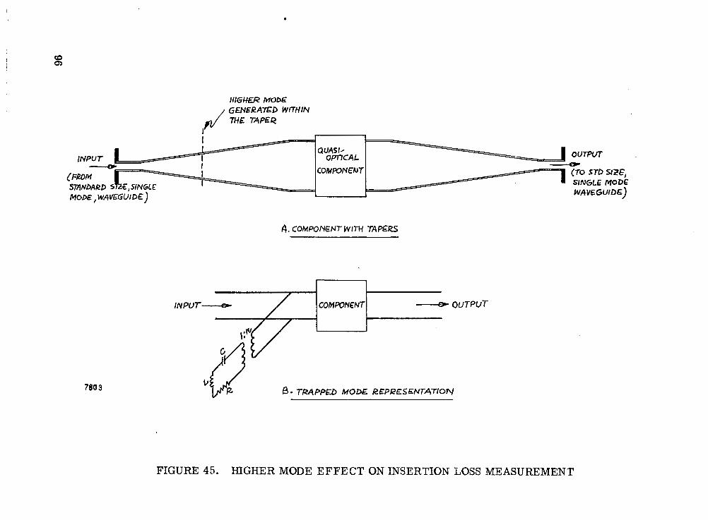
.
HIGHER MODE GENERAZD WnHlN THE TAPES
I
780 3
I (FROM (TO STD SlZE,
SINGLE MODE
M O D E , WAVEGUIDE)
.w 0- TRAPPED MODE REPPESENTATION
WAVEGUIDE)
FIGURE 45. HIGHER MODE EFFECT. ON INSERTION LOSS MEASUREMENT
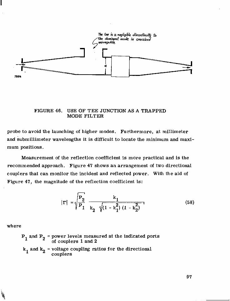
I
FIGURE 46. USE OF TEE JUNCTION AS A TRAPPED MODE FILTER
probe to avoid the launching of higher modes. Furthermore, at millimeter and submillimeter wavelengths it is difficult to locate the minimum and maxi- mum positions.
Measurement of the reflection coefficient is more practical and is the recommended approach. Figure 47 shows an arrangement of two directional couplers that can monitor the incident and reflected power. With the aid of Figure 47, the magnitude of the reflection coefficient is:
where
P and P2 = power levels measured at the indicated ports
kl and k2 = voltage coupling ratios for the directional
1 of couplers 1 and 2
couplers
97

7805
FIGURE 47. PREFERRED METHOD OF REFLECTION COEFFICIENT OR VSWR MEASUREMENT
For the case of two identical directional couplers, kl = k2 = k we have:
The VSWR is determined from Irl and i s
1
r = -
1
kl
98

Each directional coupler contains a dielectric slab placed diagonally across the center of a four-waveguide junction. The coupling ratio is a function of the slab thickness, dielectric constant, and frequency. It is equivalent to an n = 1 dielectric slab directional filter. The coupling values can thus be readily obtained from the directional filter curves given in Figure 6 of this
report.
Frequency Measurements
Frequency measurements are important in multiplier circuit work to ascertain the level of undesired harmonics and to determine the existence of parametric oscillations.
The preferred method of measuring frequency in a quasi-optical circuit is a Michaelson interferometer technique as shown in Figure 48. A double- prism coupler is used to split the available power equally into two ports that are terminated in short circuits. One short is fixed and the other is movable. A detector, connected to port 4 through a taper, notes the amplitude of the power at port 4 as a function of the position of the moving short. This varia- tion is similar to the standing wave pattern indicated in Figure 48. The sepa- ration between successive minima is A/2 o r n A/2 between the n minima.
The sharpest minima are achieved when the coupler is set for 3 db,
but it can operate reasonably well with couplings between 1 and 10 db. Thus, one can use a simpler fixed coupler, such as a single dielectric slab direc- tional filter. Its coupling will vary as a function of frequency, but it can be kept within the 1 to 10 db range for the frequencies of interest (30 t o 90 GHz).
Power Measurements
It is desirable to measure absolute power when evaluating the frequency multiplier efficiency because the multiplier efficiency is a function of the fundamental frequency power (or drive) level. The absolute power level generated at the desired harmonic is of obvious interest.
99
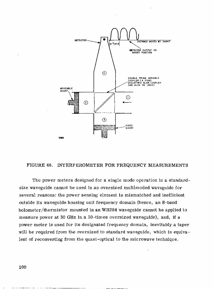
DETECTOR
DOUBLE PRISM VARIABLE COUPLER ( A FIXEC DIELECTRIC SLAB COUPLER CAN ALSO BE USED) &
- SHORT
FIGURE 48. INTERFEZOMETER FOR FREQUENCY MEASUREMENTS
The power meters designed €or a single mode operation in a standard- size waveguide cannot be used in an oversized multimoded waveguide for several reasons: the power sensing element is mismatched and inefficient outside its waveguide housing unit frequency domain (hence, an S-band
bolometer/thermistor mounted in an WR284 waveguide cannot be applied to measure power at 30 GHz in a 10-times oversized waveguide), and, if a power meter is used for its designated frequency domain, inevitably a taper will be required from the oversized to standard waveguide, which i s equiva- lent of reconverting from the quasi-optical to the microwave technique.
100
. . . . . . . " . .. . . .. . . . . . - . .. . . . .. . . .. - ... . .. . . . .. . . . . . . " """ . .. . . . "" " . . . . .
For quasi-optical power measurements a distributed power sensing element is desired which intercepts the power over the entire cross-section of the waveguide, and which is uniformly efficient over a very wide range of frequencies. Such an element had been developed at AIL in a 4H mm wave- guide (reference 18), and it has already been proposed to scale up this device to Ka-band waveguide for use in conjunction with the oversized S-band wave- guide system. This would constitute an intermediate (microwave-quasi- optical) power measuring technique, since a taper is still required, but at both waveguide sizes the multimode condition exists. The measurement procedure does not deviate from the standard microwave technique.
Loss or Efficiency Measurements
Figure 49 shows three different setups that are useful in measuring component losses. A discussion of the features of each approach follows.
The first block diagram represents a standard insertion loss measure- ment. The change in output power expressed in db is noted when the compo- nent is removed. This is also a measurement of multiplier circuit efficiency provided the detector or power meter sensitivity is known at the harmonic as well as the fundamental frequency. This setup is a lso useful in measuring the power output by employing an absolute power meter as the detector. This type of measurement is straightforward and is applicable when loss accuracy of - +O. 3 db i s adequate.
In some of our circuits it is of interest to measure losses with greater accuracy. One example is the measurement of the dissipative loss compo- nent of the two susceptance tuner. This loss may well be as little as 0.1 db. Low losses can be measured with reasonable accuracy by means of impedance circuit diagrams obtained for different positions of a moving short. Since only VSWR is convenient to ascertain in oversized waveguide, one cannot obtain this circle. It is possible however to obtain the minimum and maxi- mum VIWR which can be used to approximately estimate the dissipative loss of a component.
101

I
I SIGNAL GENERATOR
I COMPONENT I UNDER ; I
I -
a b POWER METER DETECTOR OR
A. STANDARD METHOD
INCIDENT
r 7 '
I SIGNAL GENERATOR
I ' COMPONENT : REFLECTOMETER
I I I EVALUATION ' UNDER -
I
SHORT I N a b OVERSIZED WAVEGUIDE
E. REFLECTOMETER METHOD
I COMPONENT I I UNDER I
SLdTTED LINE IN STANDARD GUIDE MODE '
FILTER 0 b
C. STANDARD GUIDE INPEDANCE METHOD
FIGURE 49. SOME LOSS MEASUREMENT METHODS
Figure 49C shows a setup for obtaining data for plotting the impedance circle from measurements taken with a standard guide slotted line. This measurement suffers from the uncertainty of the loss of the taper and mode filter.
It is however, possible to measure the loss of the taper and mode filter
separately by obtaining their impedance circle with the component removed. In each case the intrinsic or dissipative loss is determined; the difference
between the two intrinsic losses is the dissipative loss of the component.
These measurement techniques are recommended for use with actuaI
multiplier circuits and should be tried on future programs in this area.
102

CONCLUSIONS
This study of quasi-optical circuits has indicated that millimeter varac-
tor multipliers can be realized using these techniques. Directional filters
can be designed using the theory and procedures descrroed herein; agreement
with experiment is within 1 to 2 db. The-study of tuner circuits (to be used
for varactor mount matching) has indicated that the type 3 (variable suscept-
ance-variable position) tuner is preferred because it can match closest to the
source and is capable of matching a wide range of impedances. All tuner cir-
cuits should have low (<0.25 db) dissipation loss. A number of ideas for pre-
dicting the equivalent circuits of varactor mounts (both focused and array)
have been described. This must be considered as preliminary idormation
that requires experimental substantiation. Some methods for measuring fre- quency, VSWR, power, and insertion loss have been described, The findings
from this study have led to a number of suggestions for future work.
Future work in this area will now concentrate on the development of
millimeter varactor doublers using quasi-optical circuit techniques. This
mill center about the following five tasks:
1. Development of suitable directional filters
2. Development of tuners such as the variable - susceptance variable - position tuner; tuning at the fundamental and second harmonic frequen- cies. These are to be placed as close to the varactor mount as possible.
focused, array, and pa r t imy focused.
for evaluation of varactor multipliers; this in- . cludes power, impedance and frequency measure-
ments.
3. Evaluation of various varactor mounts such as
4. Development of suitable measurement techniques
103

5. Assembly of the filter, tuner, and varactor mount circuits in such a manner that efficient (consistent with available varactor characteristics) operation results.
104
1.
2.
3.
4.
5.
6.
7.
8.
9.
10.
11.
12.
REFERENCES
Copeland, J. : A New Mode of Operation for Bulk Negative Resistance Oscillators. Proc. IEEE, Vol. 54, pp. 1479-1480, Oct. 1966.
DeLoach, B. C. : Verbally reported at the 1969 Solid State Circuits Conference, Philadelphia, Pa.
Swan, C. B. : High Power CW IMPATT Oscillator Techniques. 1967 NEREM Record, p. 22, D3EE Catalog No. F-85.
Liegey, P., et. al. : Development of 50°K Uncooled Parametric Ampli- fier. Report No. 2, Contract No. DA-28-043-AMC-O2523(S), Prepared for the U, S. Army Satellite Communications Agency.
Penfield, P, and Rafuse, R. P. : Varactor Applications. The M. I. T. Press, Cambridge, Mass. 1962.
Taub, J. J., et. al. : Submillimeter Components Using Oversize Quasi- optical Waveguide: IEEE Transactions on Microwave Theory and Tech- niques, Vol. 11, Sept, 1963.
Taub, J. J. and Hindin, H. J. : Design of Quasioptical Components. Microwaves, Jan. 1964.
Taub, J. J. and Hindin, H. J. : Permittivity Measurements at Submilli- meter Wavelengths. Rev. Sci. Instr., Sept. 1963.
Taub, J. J. and Cohen, J. : Quasioptical Filters for Millimeter and Sub- millimeter Wavelengths. Proc. IEEE, Vol. 54, pp. 647-656, April 1966.
Levy, R. : Tables of Element Values for the Distributed Low-Pass Prototype Filter. lEEE Trans,, Vol. MTT-13, pp. 514-536, Sept. 1965.
Young, L. : Tables for Cascaded Homogeneous Quarter-Wave Trans- formers. IRE Trans., Vol. MTT-7, pp. 233-237, April 1959.
Corkum, R. W. : Isotropic Artificial Dielectric. Proc. IRE, Vol. 40, pp. 574-587, May 1952.

13.
14.
15.
16.
17.
1%.
B1
B2
B3
c1
Marcuvitz, N. : Waveguide Handbook. Rad. Lab. Series Vol. It?, McGraw Hill, New York, New York, 1951.
Goubau, G. and Schwering, F. : On the Guided Propagation of Electro- magnetic Wave Beams. IRE Trans. A P , Vol. 9, NO. 3, May 1961.
Kogelnick, H. and Li, T. : Laser Beams and Resonators, Proc. IRE, Vol. 54, No. 10, Oct. 1966.
Butterweck, H. J. : Mode Filters for Oversized Rectangular Wave- guides. IEEE Trans., Vol. MTT;16, pp. 274-261, May 1968.
Allen, C., Arams, F., and Bradley, C. : A Practical Detector for the Millimeter-To-Infrared Gap. IEEE Spectrum, p. 4A, Oct. 1968.
Reed, J. and Wheeler, G. J. : A Method of Analysis of Symmetrical Four-Port Networks. IRE Trans, on Microwave Theory and Tech- niques, Vol. MTT-4, pp. 246-252, Oct. 1956.
Storch, L. : The Transmission Matrix of N Alike Cascaded Networks. AIEE Trans. (Communication and Electronics), Vol. 73, pp. 616-618, Jan. 1955.
Ulrich, G., et. al. : Tunable Submillimeter Interferometers of the Fabry-Perot Type. IEEE Trans, on Microwave Theory and Tech- niques, pp. 363-371, Sept. * 1963.
106
- -~

APPENDIX A CONTRACT WORK STATEMENT
Directional Filters
The theory of quasi-optical directional filters shall be reviewed and ap- plied to directional filters compatible with multiplier requirements. Com- plete design equations and procedures shall be evolved. This will include curves and tables that will readily relate insertion loss, bandwidth, and re- jection to the dielectric constant of materials used, dielectric slab thickness, and the number of dielectric slabs. These design procedures will be appli- cable as a minimum to doublers and triplers. Application to high order multipliers will also be considered. Experimental verification of these de- sign procedures shall be provided.
Tuners
Quasi-optical tuners shall be theoretically studied, Insertion loss as a
function of VSWR to be matched shall be computed. Design details necessary for construction of these devices including mechanical and electrical toler- ances shall be presented.
Matching
A theoretical study of varactor matching and mounting techniques shall be commenced. This includes the derivation of equivalent circuits of focused and array mounts. The relative merits of various matching circuits shall be studied.
Measurement Techniques
Methods of obtaining accurate measurements of quasi-optical varactor multiplier circuits shall be analyzed and recommendations given for the
107

preferred approach. This shall include, as a minimum, impedance, absolute
power, and frequency.
108

APPENDIX B INSERTION LOSS VERSUS ELECTRICAL LENGTH OF
ITERATED DIELECTRIC-SLAB FILTERS
This appendix derives the formulas for the insertion loss versus elec- trical length of the dielectric slab filter shown in Figure 5. From Reed and Wheeler (reference Bl), the ABCD matrix for a transmission line of length d is:
where
Z = characteristic impedance of transmission line, ff = pd = electrical length of line,
= propagation constant of transmission line.
From Ramo and Whinnery (reference B2), a slab of dielectric of thick- ness d is equivalent to a transmission line of length d. The characteristic impedance of the equivalent transmission line can be written in te rms of the parameters of the dielectric.
The characteristic impedance of the equivalent transmission line for a linearly polarized wave having its electric field perpendicular to its plane of incidence on a dielectric slab, with the angle of incidence being Bi is:
1 2 0 ~ sec 8, z = 1
" K The dielectric slabs are assumed to be infinite in extent.
109

Using equation B-2, the normalized impedance Z of the other dielectric section to that of the air is:
c
Z cos Qi z =" f -
zo fr cos 0 F
(B - 3)
Using equations B-1 and B-3, the ABCD matrix of the typical iteration is :
1 ; j - sin
- [ cos flc cos fl, -Z sin 6 sin fl
[ j sin fl COS fl0
+j cos flc sin 6, ]
€ 0) 1
€
[ j sin flo cos flc + -
jz sin cos fl 01
[ -r sin sin go +
cos fic cos plo 1 - 1
03-41
If fi = fl = fl, the ABCD matrix of the iteration, equation B-4 becomes: € 0
- *E0 Bco - LC.0 D ,o j = M
110
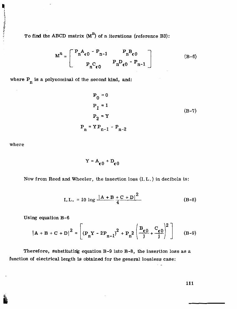
11 $1 To find the ABCD matrix (Mn) of n iterations (reference B3):
'nAc0 'n-1 'nBc 0 -
'nee 0 'nDc0 - 'n-1 1 where Pn is a polynominal of the second kind, and:
(B-6)
where
Y = Aco + DcO
Now from Reed and Wheeler, the insertion loss (I. L. ) in decibels is:
2 A + B + C + D I 4 I.L. = 10 log '
Using equation B-6
Therefore, substitutirig equation B-9 into B-8, the insertion loss as a
function of electrical length is obtained for the general lossless case: . _
111
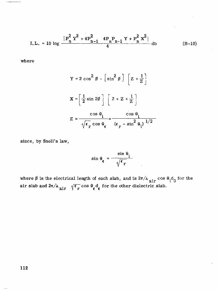
I.L. = 10 log n n-1 4 db
where
~ = 2 c o s 2 $ - [sin 2 $ 1 [ Z + % J 1 1
L J L J
cos Qi cos 0 Z = -" i
Fr cos Qc -
2 1/2 ( c r - sin Qi)
since, by Snell's law,
sin 0,
(B-10)
where $ is the electrical length of each slab, and is 27/A air cos €lid0 for the air slab and 2a/h air c cos 0 d for the other dielectric slab. G € €
112

APPENDM C QUASI- OPTICAL STRIP GRATING CIRCUIT
If the electric field is incident as shown in Figure 27A and the metal strips are in an air dielectric, we have an inductive grating; its equivalent circuit (normalized to the intrinsic impedance of free space) is shown in Figure 27B. Approximate formulas for x and r are given in reference C1; when it is assumed that y << X, the formulas are:
X = w v/X and r = - S Y ' r l UX
where
w = .tn csc (7~ a/r) s = Skin depth u = Strip perimeter = 4a + 2t 4a for a >> t a = Strip width y = Center to center spacing of strips
It is also convenient to define a Q factor equal to x/r. For a copper grating, s = 6.62 f hence
Q = (4a + 2 t) tn csc (IT a/v) 6.62 - IT - "-iT f
where a, g, and t are expressed in cm. For our tuner analysis we have chosen b = 2 or x = 1/2. For this case Q simplifies to
Q = (2a + t) X
6.62 IT f - l l 2 (C - 3)
. 113

10 For y / A = 1/2 and f = 3 x 10 Hz, we have for b = 2 and t c< 2a, the condition that a/y = 1/7. Substituting these values yields a Q = 2500. The normalized shunt resistance is Q o r 1250; the theoretical normalized con-
ductance is 8 x In practice the Q factor will be lower due to surface roughness and some diffraction losses; a Q of 1500 is a realistic value.
114 .

APPENDM D MATCHING BY TWO VARIABLE SUSCEPTANCES
SEPARATED BY A FMED LENGTH
Consider the equivalent circuit of Figure 29. Two variable SusceP- tances bl and b2 are separated by a line of electrical length 8 ; we wish to
determine the range of load admittances, YL = g + jb, that can be matched. The match condition is to force Yaa (the admittance looking to the left of aa) to equal the conjugate of YE.
Using transmission line theory one obtains
1 - j (1 - bl) Y = jb2 + -
aa (1 + bl) - j - gaa + jbaa
o r
2 - - -
2 + 2bl + bl 2
and
2 b,
b = b 2 + 1 aa 2 2 + 2bl + bl
115
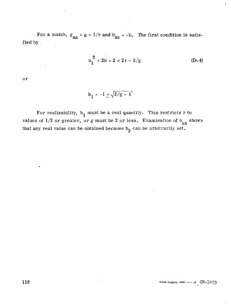
For a match, g = g = l/r and baa = -b. The first condition is satis- aa fied.by /
b 2 + 2 b + 2 = 2 r = 2 / g 1
o r
For realizability, b must be a real quantity. This res t r ic ts r to
values of 1/2 or greater, o r g must be 2 o r less. Examination of b shows
that any real value can be obtained because b2 can be arbitrarily set.
1 aa
116 NASA-Langley, 1969 - 10 CR-1453