October 11, 20001. 2 Design Consideration USB2 PHY Core Patrick Yu inSilicon Corporation...
26
October 11, 2000 1
-
Upload
cuthbert-black -
Category
Documents
-
view
214 -
download
1
Transcript of October 11, 20001. 2 Design Consideration USB2 PHY Core Patrick Yu inSilicon Corporation...

October 11, 2000 1

October 11, 2000 2
Design Consideration USB2 PHY Core
Design Consideration USB2 PHY Core
Patrick YuPatrick YuinSilicon CorporationinSilicon Corporation
October 11, 2000 3
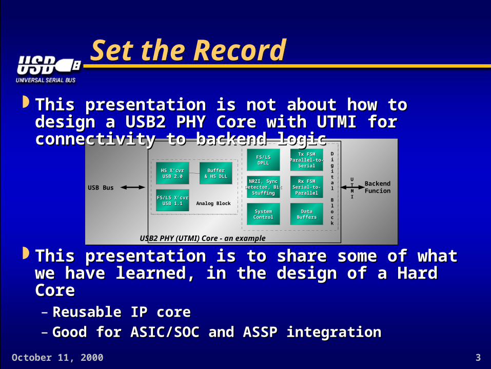
FS/LSFS/LSDPLLDPLL
NRZI, SyncNRZI, SyncDetector, BitDetector, Bit
StuffingStuffing
Tx FSMTx FSMParallel-to-Parallel-to-
SerialSerial
Rx FSMRx FSMSerial-to-Serial-to-ParallelParallel
SystemSystemControlControl
DataDataBuffersBuffers
Digital
Block
UTMI
HS X'cvrHS X'cvrUSB 2.0USB 2.0
FS/LS X'cvrFS/LS X'cvrUSB 1.1USB 1.1
BufferBuffer& HS DLL& HS DLL
Analog Block
USB2 PHY (UTMI) Core - an example
USB BusBackendFuncion
Set the RecordSet the Record
This presentation is not about how to design a USB2 PHY This presentation is not about how to design a USB2 PHY Core with UTMI for connectivity to backend logicCore with UTMI for connectivity to backend logic
This presentation is to share some of what we have This presentation is to share some of what we have learned, in the design of a Hard Corelearned, in the design of a Hard Core– Reusable IP core Reusable IP core – Good for ASIC/SOC and ASSP integrationGood for ASIC/SOC and ASSP integration

October 11, 2000 4
ContentContent
System-level ConsiderationSystem-level Consideration
Core-level ConsiderationCore-level Consideration
Testability ConsiderationTestability Consideration
““Ease of Integration” ConsiderationEase of Integration” Consideration
SummarySummary

October 11, 2000 5
System-Level ConsiderationSystem-Level Consideration
How would the PHY be used?How would the PHY be used?– Host Controller, Hub Controller, Function ControllerHost Controller, Hub Controller, Function Controller– Application specific or SOCApplication specific or SOC

October 11, 2000 6
System-Level ConsiderationSystem-Level Consideration
Characteristics of the applicationsCharacteristics of the applications– Host Controller, when integrated into a PC core logic, Host Controller, when integrated into a PC core logic,
needs to support 5 to 8 portsneeds to support 5 to 8 ports When integrated into a CE devices like STB and residential When integrated into a CE devices like STB and residential
gateway, needs 1 to 3 portsgateway, needs 1 to 3 ports– Function Controller is usually application specificFunction Controller is usually application specific
The system environment could be space limited,The system environment could be space limited,e.g. still camerae.g. still camera
The applications typically require only one portThe applications typically require only one port Usually very concerned with the cost of passive Usually very concerned with the cost of passive
components needed, as well as system costcomponents needed, as well as system cost
ContinuedContinued

October 11, 2000 7
System-Level ConsiderationSystem-Level Consideration
Influence of these characteristics on PHY’s featuresInfluence of these characteristics on PHY’s features– 3 speeds: LS @ 1.5Mbps, FS @ 12Mbps, HS @ 480Mbps3 speeds: LS @ 1.5Mbps, FS @ 12Mbps, HS @ 480Mbps– Support low-cost crystal for Function Controller, clock Support low-cost crystal for Function Controller, clock
generator for Host Controllergenerator for Host Controller Cost difference is typically of 2XCost difference is typically of 2X
– On-chip terminationOn-chip termination Saving of 2 pins per port for Host Controller applicationSaving of 2 pins per port for Host Controller application Driver input-impedance variation of + 10% for HS become non-Driver input-impedance variation of + 10% for HS become non-
issueissue Cleaner signal for the receiverCleaner signal for the receiver
– Integration of “pull-up resistors” could improve timingIntegration of “pull-up resistors” could improve timing

October 11, 2000 8
System-Level ConsiderationSystem-Level Consideration
What about power?What about power?– Can USB 2.0 peripherals ever be bus-powered ?Can USB 2.0 peripherals ever be bus-powered ?
Probably “not” for discrete USB 2.0 Hub !Probably “not” for discrete USB 2.0 Hub !– Current budget for LDO & switch-mode regulators, Current budget for LDO & switch-mode regulators,
passive components, electro-mechanicals, electronics, passive components, electro-mechanicals, electronics,

October 11, 2000 9
Current Consumption: ChipsCurrent Consumption: ChipsSystem-Level ConsiderationSystem-Level Consideration
USB Semiconductor Devices USB Semiconductor Devices
USB1.1 Audio ASSPUSB1.1 Audio ASSPPhilips UDA1331HPhilips UDA1331H
50mA @ 3.3V max50mA @ 3.3V max 48MHz crystal oscillator:48MHz crystal oscillator:startup current @ 15mAstartup current @ 15mAtypical operating current @ 2.1mA typical operating current @ 2.1mA
USB1.1 I/F Device ASSPUSB1.1 I/F Device ASSPPhilips PDIUSBD12Philips PDIUSBD12
15mA @ 3.6~5.5V operational;15mA @ 3.6~5.5V operational;15mA when suspended with 15mA when suspended with oscillator offoscillator off
6MHz crystal oscillator (clock 6MHz crystal oscillator (clock multiplying PLL to 48MHz)multiplying PLL to 48MHz)
USB2.0 PHY ASSPUSB2.0 PHY ASSPPhilips ISP1501Philips ISP1501
FS transmit & receive @ 6mAFS transmit & receive @ 6mAHS receive @ 54mA max.HS receive @ 54mA max.HS transmit @ 100mA max.HS transmit @ 100mA max.Suspend mode @ 40Suspend mode @ 40mmA max.A max.
12MHz crystal input (internal to 30MHz 12MHz crystal input (internal to 30MHz & 480MHz)& 480MHz)
Power Switch - MIC2075Power Switch - MIC2075Micrel Semiconductor Micrel Semiconductor
Max. supply current @ 160Max. supply current @ 160mmAAO/P leakage current @ 10O/P leakage current @ 10mmAA
for Host & Hub applicationsfor Host & Hub applications
LDO Regulator – MIC5207LDO Regulator – MIC5207Micrel Semiconductor Micrel Semiconductor
Quiescent current = 0.01 ~ 5Quiescent current = 0.01 ~ 5mmAAGround pin current @ IGround pin current @ ILL = =
100100mmA: 80A: 80mmA ~ 170A ~ 170mmA;A;Ground pin current @ IGround pin current @ ILL = =
100mA: 720100mA: 720mmA ~ 2mA;A ~ 2mA;Ground pin current @ IGround pin current @ ILL = =
150mA: 1.8mA ~ 3mA150mA: 1.8mA ~ 3mA
for Peripheral applicationsfor Peripheral applications

October 11, 2000 10
System-Level ConsiderationSystem-Level ConsiderationCurrent Consumption: DevicesCurrent Consumption: Devices
USB Peripheral Devices USB Peripheral Devices
SanDisk CompactFlashSanDisk CompactFlash(8 ~ 300Mbytes)(8 ~ 300Mbytes)
32~45mA @ 3.3V read32~45mA @ 3.3V read46~75mA @ 5V46~75mA @ 5V32~60mA @ 3.3V write32~60mA @ 3.3V write46~90mA @ 5V46~90mA @ 5V
SanDisk MM CardSanDisk MM Card(4 ~ 32Mbytes)(4 ~ 32Mbytes)
< 33mA @ 3.3V read< 33mA @ 3.3V read< 23mA @ 2.7V< 23mA @ 2.7V< 35mA @ 3.3V read< 35mA @ 3.3V read< < 27mA @ 2.7V27mA @ 2.7V
LexarMedia CflashLexarMedia Cflash(160 ~ 256Mbytes)(160 ~ 256Mbytes)
65mA @ 5V read/write65mA @ 5V read/write45mA @ 3.3V read/write45mA @ 3.3V read/write
IBM Compact Flash IBM Compact Flash ReaderReader
255mA @ 5V255mA @ 5V www.apricorn.comwww.apricorn.com
Iomega Zip 250Iomega Zip 250 ~ 450mA @ 5V (moving to ~ 450mA @ 5V (moving to 3.3V)3.3V)
Design uses switch-mode Design uses switch-mode regulatorregulator
USB-to-10/100 Ethernet USB-to-10/100 Ethernet BridgeBridge
285mA @ 5V285mA @ 5V450mA @ 3.3V450mA @ 3.3V
www.linksys.comwww.linksys.comwww.cadmusmicro.comwww.cadmusmicro.com
USB-to-10Mbps Ethernet USB-to-10Mbps Ethernet BridgeBridge
120mA @ 5V120mA @ 5V www.silicom.co.ilwww.silicom.co.il
USB-to-56K modemUSB-to-56K modem 40mA Full-ON Mode40mA Full-ON Mode< 0.5mA Sleep Mode< 0.5mA Sleep Mode
www.sharkmm.comwww.sharkmm.com

October 11, 2000 11
SummarySummarySystem-Level ConsiderationSystem-Level Consideration
Pin-count and termination are important for Host Pin-count and termination are important for Host Controller, but ……Controller, but ……
High-power bus-powered USB 2.0 peripherals are High-power bus-powered USB 2.0 peripherals are feasible, but watch for current budgetfeasible, but watch for current budget– Consumption by transmitter, receiver, oscillator circuitry, PLL, Consumption by transmitter, receiver, oscillator circuitry, PLL,
DLL, DPLL, 5V short-circuit protectionDLL, DPLL, 5V short-circuit protection Un-initialized mode budget of 100mAUn-initialized mode budget of 100mA Initialized mode budget of 500mAInitialized mode budget of 500mA Suspend mode of 500mA or 2.5mASuspend mode of 500mA or 2.5mA
– Consumption of LDO or Switch-mode regulatorConsumption of LDO or Switch-mode regulator– Voltage drop across passive componentsVoltage drop across passive components

October 11, 2000 12
Core-Level ConsiderationCore-Level ConsiderationArchitectureArchitecture
Data -Data -Data -Data -----
HS XCVRHS XCVRHS XCVRHS XCVR
FS/LS XCVRFS/LS XCVRFS/LS XCVRFS/LS XCVR
RcvRcvRcvRcv
XmitXmitXmitXmit
Status/Status/Status/Status/ControlControlControlControl
RcvRcvRcvRcv
XmitXmitXmitXmit
Status/Status/Status/Status/ControlControlControlControl
NRZINRZINRZINRZIEncoderEncoderEncoderEncoder
BitBitBitBitStufferStufferStufferStuffer
Data+Data+Data+Data+
ParallelParallelParallelParallelDataDataDataData
ControlControlControlControl
ClockClockClockClockMultiplierMultiplierMultiplierMultiplier
CLKCLKCLKCLK
ReceiveReceiveReceiveReceiveStateStateStateState
MachineMachineMachineMachine
TransmitTransmitTransmitTransmitStateStateStateState
MachineMachineMachineMachine
(E)(E)(E)(E)(F)(F)(F)(F)
ExternalExternalExternalExternalCrystalCrystalCrystalCrystal
SystemSystemSystemSystemControlControlControlControlLogicLogicLogicLogic
HSHSHSHSDLLDLLDLLDLL
FSFSFSFSDPLLDPLLDPLLDPLL
ElasticityElasticityElasticityElasticityBufferBufferBufferBuffer syncsyncsyncsync
detectordetectordetectordetector
RxRxRxRxShiftShiftShiftShiftRegRegRegReg
RxRxRxRxHoldHoldHoldHoldRegRegRegReg
NRZINRZINRZINRZIDecoderDecoderDecoderDecoder
(B)(B)(B)(B)
UnstufferUnstufferUnstufferUnstufferBitBitBitBit
MuxMuxMuxMux
MixedMixedMixedMixedsignalsignalsignalsignal
InterfaceInterfaceInterfaceInterface
UUUUTTTTMMMMIIII
MIXED SIGNALMIXED SIGNALMIXED SIGNALMIXED SIGNALBLOCKBLOCKBLOCKBLOCK
DIGITALDIGITAL DIGITALDIGITALBLOCKBLOCKBLOCKBLOCK
TxTxTxTxShiShiShiShiftftftftRegRegRegReg
TxTxTxTxHoldHoldHoldHoldRegRegRegReg
October 11, 2000 13
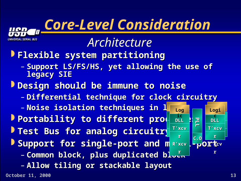
Core-Level ConsiderationCore-Level Consideration
Flexible system partitioningFlexible system partitioning– Support LS/FS/HS, yet allowing the use of legacy SIESupport LS/FS/HS, yet allowing the use of legacy SIE
Design should be immune to noiseDesign should be immune to noise– Differential technique for clock circuitryDifferential technique for clock circuitry– Noise isolation techniques in layoutNoise isolation techniques in layout
Portability to different processesPortability to different processes Test Bus for analog circuitryTest Bus for analog circuitry Support for single-port and multi-portSupport for single-port and multi-port
– Common block, plus duplicated blockCommon block, plus duplicated block– Allow tiling or stackable layoutAllow tiling or stackable layout
DLLDLL
T’xcvrT’xcvr
R’xcvrR’xcvr
Logic
PLLPLL
C.O.C.O.
DLLDLL
T’xcvrT’xcvr
R’xcvrR’xcvr
Logic
ArchitectureArchitecture

October 11, 2000 14
UTMIUTMI
USB 1.1 USB 1.1 UHCI / OHCIUHCI / OHCI
USB 1.1 USB 1.1 UHCI / OHCIUHCI / OHCI
SIESIESIESIE
USB 1.1 USB 1.1 UHCI / OHCIUHCI / OHCI
USB 1.1 USB 1.1 UHCI / OHCIUHCI / OHCI
SIESIESIESIE
USB 1.1 USB 1.1 UHCI / OHCIUHCI / OHCI
USB 1.1 USB 1.1 UHCI / OHCIUHCI / OHCI
SIESIESIESIE
UTMI* PHY (digital)UTMI* PHY (digital)UTMI* PHY (digital)UTMI* PHY (digital)
UTMI PHY (mixed-signal)UTMI PHY (mixed-signal)UTMI PHY (mixed-signal)UTMI PHY (mixed-signal)
UTMI* PHY (digital)UTMI* PHY (digital)UTMI* PHY (digital)UTMI* PHY (digital)
UTMI PHY (mixed-signal)UTMI PHY (mixed-signal)UTMI PHY (mixed-signal)UTMI PHY (mixed-signal)
UTMI* PHY (digital)UTMI* PHY (digital)UTMI* PHY (digital)UTMI* PHY (digital)
UTMI PHY (mixed-signal)UTMI PHY (mixed-signal)UTMI PHY (mixed-signal)UTMI PHY (mixed-signal)
UTMIUTMIUTMIUTMIUTMIUTMIUTMIUTMI
UTMIUTMIUTMIUTMI
USB 2.0 EHCIUSB 2.0 EHCI
Core-Level ConsiderationCore-Level Consideration
UTMI is a direct fit for HS/FS peripheral UTMI is a direct fit for HS/FS peripheral applicationapplication
UTMI* for host applicationUTMI* for host application– Additional signals are needed to support multi ports Additional signals are needed to support multi ports
and hybrid OHCI / UHCI & EHCI implementationand hybrid OHCI / UHCI & EHCI implementation For example, direct access to FS/LS transceivers by legacy For example, direct access to FS/LS transceivers by legacy
SIE of USB1.1 Host ControllerSIE of USB1.1 Host Controller

October 11, 2000 15
UTMIUTMICore-Level ConsiderationCore-Level Consideration
UTMI* for OHCI / UHCI and EHCI for direct UTMI* for OHCI / UHCI and EHCI for direct connection to the individual UTMI* PHYsconnection to the individual UTMI* PHYs
UTMIUTMIUTMIUTMIUTMIUTMIUTMIUTMI
UTMI*UTMI*UTMI*UTMI*
USB 1.1 USB 1.1 UHCI / OHCIUHCI / OHCI
USB 1.1 USB 1.1 UHCI / OHCIUHCI / OHCIUSB 1.1 USB 1.1
UHCI / OHCIUHCI / OHCIUSB 1.1 USB 1.1
UHCI / OHCIUHCI / OHCIUSB 1.1 USB 1.1 UHCI / OHCIUHCI / OHCI
USB 1.1 USB 1.1 UHCI / OHCIUHCI / OHCI UTMIUTMIUTMIUTMI
UTMIUTMIUTMIUTMIUTMIUTMIUTMIUTMI
USB 2.0 EHCIUSB 2.0 EHCI
UTMI* PHY (digital)UTMI* PHY (digital)UTMI* PHY (digital)UTMI* PHY (digital)
UTMI PHY (mixed-signal)UTMI PHY (mixed-signal)UTMI PHY (mixed-signal)UTMI PHY (mixed-signal)
UTMI* PHY (digital)UTMI* PHY (digital)UTMI* PHY (digital)UTMI* PHY (digital)
UTMI PHY (mixed-signal)UTMI PHY (mixed-signal)UTMI PHY (mixed-signal)UTMI PHY (mixed-signal)
UTMI* PHY (digital)UTMI* PHY (digital)UTMI* PHY (digital)UTMI* PHY (digital)
UTMI PHY (mixed-signal)UTMI PHY (mixed-signal)UTMI PHY (mixed-signal)UTMI PHY (mixed-signal)
October 11, 2000 16
TransceiversTransceiversCore-Level ConsiderationCore-Level Consideration
Fully staticFully static– The receiver will remain off until the packet The receiver will remain off until the packet
transmission is donetransmission is done Careful with the control timings, because small overlap of Careful with the control timings, because small overlap of
the receiver and transmitter on-timing will be necessarythe receiver and transmitter on-timing will be necessary Turning off the DLL certainly help, but what aboutTurning off the DLL certainly help, but what about
turn-on time ?turn-on time ?– Receivers must accommodate a wide range of Receivers must accommodate a wide range of
common mode voltage while within the common mode voltage while within the sensitivity/threshold spec for LS/FS/HSsensitivity/threshold spec for LS/FS/HS

October 11, 2000 17
Transceivers ContinuedTransceivers ContinuedCore-Level ConsiderationCore-Level Consideration
Transmitter should provide the highestTransmitter should provide the highestquality signalquality signal– Matching the rise time and fall time are trickyMatching the rise time and fall time are tricky
Multi-phase turn-on enable symmetrical outputMulti-phase turn-on enable symmetrical output– Eliminate as much jitter as possible from the outputEliminate as much jitter as possible from the output
Power consumption is critical for bus-powered Power consumption is critical for bus-powered applicationsapplications– 3.3V voltage source are necessary to interface 5V 3.3V voltage source are necessary to interface 5V
tolerant I/Ostolerant I/Os– 5v short-circuit protection unfriendly to5v short-circuit protection unfriendly to
low-voltage processlow-voltage process

October 11, 2000 18
Core-Level ConsiderationCore-Level Consideration
Common PLL block to supply 480MHz clock to the restCommon PLL block to supply 480MHz clock to the rest– Any jitter in the PLL will propagate to the other blocksAny jitter in the PLL will propagate to the other blocks
PLL is a low-pass filter, hence any jitter of the reference clock matterPLL is a low-pass filter, hence any jitter of the reference clock matter– All differential design will increase powerAll differential design will increase power
consumptionconsumption– Clock distribution: balanced and synchronousClock distribution: balanced and synchronous– Start-up time could be criticalStart-up time could be critical
ClocksClocks
Phase Interpolator provides phase Phase Interpolator provides phase increment (single-ended) of PLL synthesized increment (single-ended) of PLL synthesized clock (pecl differential)clock (pecl differential)– Interpolates between taps of the VCO to facilitate Interpolates between taps of the VCO to facilitate
digital clock recovery at DLLdigital clock recovery at DLL– Non-linearity of transfer function does not matter Non-linearity of transfer function does not matter
as long as maximum tap size is small enoughas long as maximum tap size is small enough
PECL to CMOSConverters
PECL PH0
PECL PH1
PECL PH2
PECL PH3
PECL PH4
CMOS PH0
CMOS PH1
CMOS PH2
CMOS PH3
CMOS PH4
CMOS PH5
CMOS PH6
CMOS PH7
CMOS PH8
CMOS PH9
CMOS PH10
CMOS PH11
CMOS PH12
CMOS PH13
CMOS PH14
CMOS PH15
CMOS PH16
CMOS PH17
CMOS PH18
CMOS PH19

October 11, 2000 19
ClocksClocks
Core-Level ConsiderationCore-Level Consideration
DLL for high-speed digital designDLL for high-speed digital design– Recover the 480MHz clock from the incoming HS dataRecover the 480MHz clock from the incoming HS data– Lock to the sync pattern must be within 12 HS bit timesLock to the sync pattern must be within 12 HS bit times
DPLL for full/low-speed: low-speed digitalDPLL for full/low-speed: low-speed digital– Over-sample the incoming FS/LS data @ 48MHzOver-sample the incoming FS/LS data @ 48MHz

October 11, 2000 20
Clocks ContinuedClocks ContinuedCore-Level ConsiderationCore-Level Consideration
Oscillator circuitry for crystalOscillator circuitry for crystal– Amplifier design approach provides better control of Amplifier design approach provides better control of
crystal drive and more predictable performance over crystal drive and more predictable performance over supply voltage noisesupply voltage noise
– Small start-up current and nominal operating current Small start-up current and nominal operating current consumptionconsumption
– Usable output a.s.a.pUsable output a.s.a.p

October 11, 2000 21
Core-level ConsiderationCore-level Consideration
Design should be immune to noiseDesign should be immune to noise– Differential techniqueDifferential technique
Isolation technique applied during layout of the Hard CoreIsolation technique applied during layout of the Hard Core– Clean external voltage sourceClean external voltage source– On-chip de-coupling capacitors to reduceOn-chip de-coupling capacitors to reduce
impact of supply noiseimpact of supply noise– Substrate separation ?Substrate separation ?– Sea-Wall to isolate the high-speedSea-Wall to isolate the high-speed
analog blocksanalog blocks– Triple-well process, but expensiveTriple-well process, but expensive
Noise ContainmentNoise Containment
VVDDDDVVDDDD
Nwell-ringNwell-ringNwell-ringNwell-ring
Psub-ringPsub-ringPsub-ringPsub-ring
Analog CircuitsAnalog CircuitsAnalog CircuitsAnalog CircuitsPsub-ringPsub-ringPsub-ringPsub-ring
VVSSSS**VVSSSS**
VVSSSSVVSSSS

October 11, 2000 22
Analog IP CoreAnalog IP CoreTestability ConsiderationTestability Consideration
Debugging and VerificationDebugging and Verification– Test Bus for analog circuitryTest Bus for analog circuitry
Tap into key points of analog circuitry to measure voltage, Tap into key points of analog circuitry to measure voltage, current, resistance, etc.current, resistance, etc.
Multiplexed with other primary I/Os of the chip should be ok, Multiplexed with other primary I/Os of the chip should be ok, but, never cut corner as they can be business threatening but, never cut corner as they can be business threatening
– Push vs PullPush vs Pull BIST cost gates and not vendor-neutralBIST cost gates and not vendor-neutral ““Loop-back + Stopping Clock + Scan-chain”Loop-back + Stopping Clock + Scan-chain”
UTMI Test ModesUTMI Test Modes
October 11, 2000 23
Analog IP CoreAnalog IP CoreTestability ConsiderationTestability Consideration
Support for manufacturingSupport for manufacturing– Full scan (difficult for high-speed digital circuitryFull scan (difficult for high-speed digital circuitry
like DLL & elasticity buffer)like DLL & elasticity buffer)– Loop-back logics to automate transmitter andLoop-back logics to automate transmitter and
receiver testingreceiver testing– PLL bypassPLL bypass– Functional test vectors optimized for tester timeFunctional test vectors optimized for tester time– Corner-case analysisCorner-case analysis
Verification with Test Chip & USB PlugFestVerification with Test Chip & USB PlugFest

October 11, 2000 24
Analog IP CoreAnalog IP Core
“Ease of Integration” Consideration“Ease of Integration” Consideration
USB2 PHY Core is a high-speed AnalogUSB2 PHY Core is a high-speed AnalogPHY IP CorePHY IP Core– Would licensees want a “hard” or “soft” core?Would licensees want a “hard” or “soft” core?
Hard Core is process/library dependentHard Core is process/library dependent Soft Core is process/library INdependentSoft Core is process/library INdependent
– Can design database – GDSII – be simply drop in?Can design database – GDSII – be simply drop in? Layout and placementLayout and placement Test signals routingTest signals routing

October 11, 2000 25
Analog IP Core ContinuedAnalog IP Core Continued
“Ease of Integration” Consideration“Ease of Integration” Consideration
USB2 PHY Core is a high-speed AnalogUSB2 PHY Core is a high-speed AnalogPHY IP CorePHY IP Core– Would licensees need to do circuit tweak forWould licensees need to do circuit tweak for
different fab. @ same process?different fab. @ same process? Impact on the scope of deliverablesImpact on the scope of deliverables
– Is the analog circuitry susceptible to digital Is the analog circuitry susceptible to digital switching noises ?switching noises ? On-chip decoupling capacitors, triple-well process,On-chip decoupling capacitors, triple-well process,
sea-wall layout, ……sea-wall layout, ……– How to identify problem on a “finished” design: SOC ?How to identify problem on a “finished” design: SOC ?
Test Buses, full-scan, loop-back…….Test Buses, full-scan, loop-back…….

October 11, 2000 26
SummarySummary
UTMI-compliant PHY IP Core is a sophisticated designUTMI-compliant PHY IP Core is a sophisticated design– Hard Core is fool-proof for integration purposeHard Core is fool-proof for integration purpose– Soft Core is difficult to use and requires substantial in-house Soft Core is difficult to use and requires substantial in-house
analog expertiseanalog expertise Correct design consideration mean a good re-usable IP Correct design consideration mean a good re-usable IP
Hard CoreHard Core– Careful planning of feature objective before committing your Careful planning of feature objective before committing your
internal resource and development scheduleinternal resource and development schedule– Consult your provider (internal or external) in detail before Consult your provider (internal or external) in detail before
committing your resource and money committing your resource and money No zero TCO please !No zero TCO please !
It is important for the consumers and the providers of the It is important for the consumers and the providers of the PHY IP Core to have the right expectationPHY IP Core to have the right expectation