Obsolete Product(s) - Obsolete Product(s) · TDA2050 32 W hi-fi audio power amplifier Features High...
18
August 2011 Doc ID 1461 Rev 3 1/18 18 TDA2050 32 W hi-fi audio power amplifier Features ■ High output power (50 W music power IEC 268.3 rules) ■ High operating supply voltage (50 V) ■ Single or split supply operations ■ Very low distortion ■ Short-circuit protection (OUT to GND) ■ Thermal shutdown Description The TDA 2050 is a monolithic integrated circuit in a Pentawatt package, intended for use as an audio class-AB audio amplifier. Thanks to its high power capability the TDA2050 is able to provide up to 35 W true RMS power into a 4 ohm load at THD = 0%, V S = ±18 V, f = 1 kHz and up to 32 W into an 8 ohm load at THD = 10%, V S = ±22 V, f = 1 kHz. Moreover, the TDA2050 delivers typically 50 W music power into a 4 ohm load over 1 sec at V S = 22.5 V, f = 1 kHz. The high power and very low harmonic and crossover distortion (THD = 0.05% typ, at V S = ±22 V, P O = 0.1 to 15 W, R L = 8 ohm, f = 100 Hz to 15 kHz) make the device most suitable for both hi-fi and high-end TV sets. Figure 1. Test and application circuit Table 1. Device summary Order code Package TDA2050V Pentawatt vertical Pentawatt V www.st.com Obsolete Product(s) - Obsolete Product(s)
Transcript of Obsolete Product(s) - Obsolete Product(s) · TDA2050 32 W hi-fi audio power amplifier Features High...

August 2011 Doc ID 1461 Rev 3 1/18
18
TDA2050
32 W hi-fi audio power amplifier
Features■ High output power
(50 W music power IEC 268.3 rules)
■ High operating supply voltage (50 V)
■ Single or split supply operations
■ Very low distortion
■ Short-circuit protection (OUT to GND)
■ Thermal shutdown
DescriptionThe TDA 2050 is a monolithic integrated circuit in a Pentawatt package, intended for use as an audio class-AB audio amplifier.
Thanks to its high power capability the TDA2050 is able to provide up to 35 W true RMS power into a 4 ohm load at THD = 0%, VS = ±18 V, f = 1 kHz and up to 32 W into an 8 ohm load at THD = 10%, VS = ±22 V, f = 1 kHz.
Moreover, the TDA2050 delivers typically 50 W music power into a 4 ohm load over 1 sec at VS = 22.5 V, f = 1 kHz.
The high power and very low harmonic and crossover distortion (THD = 0.05% typ, at VS = ±22 V, PO = 0.1 to 15 W, RL= 8 ohm, f = 100 Hz to 15 kHz) make the device most suitable for both hi-fi and high-end TV sets.
Figure 1. Test and application circuit
Table 1. Device summary
Order code Package
TDA2050V Pentawatt vertical
Pentawatt V
www.st.com
O
bsolete Product(
s) - O
bsolete Product(
s)
Device overview TDA2050
2/18 Doc ID 1461 Rev 3
1 Device overview
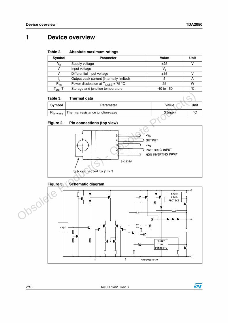
Table 2. Absolute maximum ratings
Table 3. Thermal data
Figure 2. Pin connections (top view)
Figure 3. Schematic diagram
Symbol Parameter Value Unit
Vs Supply voltage ±25 V
Vi Input voltage Vs
Vi Differential input voltage ±15 V
Io Output peak current (internally limited) 5 A
Ptot Power dissipation at TCASE = 75 °C 25 WTstg, Tj Storage and junction temperature -40 to 150 °C
Symbol Parameter Value Unit
Rth j-case Thermal resistance junction-case 3 (max) °C
O
bsolete Product(
s) - O
bsolete Product(
s)
TDA2050 Device overview
Doc ID 1461 Rev 3 3/18
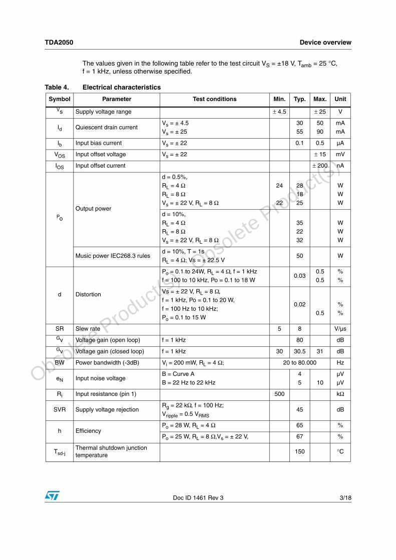
The values given in the following table refer to the test circuit VS = ±18 V, Tamb = 25 °C, f = 1 kHz, unless otherwise specified.
Table 4. Electrical characteristics
Symbol Parameter Test conditions Min. Typ. Max. Unit
Vs Supply voltage range ± 4.5 ± 25 V
Id Quiescent drain currentVs = ± 4.5Vs = ± 25
3055
5090
mAmA
Ib Input bias current Vs = ± 22 0.1 0.5 µA
VOS Input offset voltage Vs = ± 22 ± 15 mV
IOS Input offset current ± 200 nA
Po
Output power
d = 0.5%, RL = 4 ΩRL = 8 ΩVs = ± 22 V, RL = 8 Ω
24
22
28
18
25
W
W
W
d = 10%,
RL = 4 ΩRL = 8 ΩVs = ± 22 V, RL = 8 Ω
35
2232
W
WW
Music power IEC268.3 rulesd = 10%, T = 1sRL = 4 Ω; Vs = ± 22.5 V
50 W
d Distortion
Po = 0.1 to 24W, RL = 4 Ω, f = 1 kHz f = 100 to 10 kHz, Po = 0.1 to 18 W
0.030.50.5
%%
Vs = ± 22 V, RL = 8 Ω,f = 1 kHz, Po = 0.1 to 20 W,
f = 100 Hz to 10 kHz;
Po = 0.1 to 15 W
0.020.5
%%
SR Slew rate 5 8 V/µs
Gv Voltage gain (open loop) f = 1 kHz 80 dB
Gv Voltage gain (closed loop) f = 1 kHz 30 30.5 31 dB
BW Power bandwidth (-3dB) Vi = 200 mW, RL = 4 Ω; 20 to 80.000 Hz
eN Input noise voltageB = Curve A
B = 22 Hz to 22 kHz
4
5 10
µV
µV
Ri Input resistance (pin 1) 500 kΩ
SVR Supply voltage rejectionRg = 22 kΩ, f = 100 Hz;Vripple = 0.5 VRMS
45 dB
h EfficiencyPo = 28 W, RL = 4 Ω 65 %
Po = 25 W, RL = 8 Ω,Vs = ± 22 V, 67 %
Tsd-jThermal shutdown junction temperature
150 °C
O
bsolete Product(
s) - O
bsolete Product(
s)

Device overview TDA2050
4/18 Doc ID 1461 Rev 3
Figure 4. Split-supply typical application circuit
Figure 5. PC board and component layout of split-supply typical application circuit
R3
R2
R1
C2
C4
C3
R4
C5
C6
C1
C7+Vs
R L
-Vs
TDA2050
Vi
O
bsolete Product(
s) - O
bsolete Product(
s)

TDA2050 Split-supply application suggestions
Doc ID 1461 Rev 3 5/18
2 Split-supply application suggestions
The recommended values of the external components are those shown on the application circuit of Figure 5. Different values can be used. The following table can help the designer.
Table 5. Recommended values of external components
ComponentRecommended
valuePurpose
Larger thanrecommended value
Smaller thanrecommended value
R1 22 kΩ Input impedanceIncrease of input impedance
Decrease of Input Impedance
R2 680 ΩFeedback resistor
Decrease of gain(1)
1. The gain must be higher than 24 dB
Increase of gain
R3 22 kΩ Increase of gain Decrease of gain(1)
R4 2.2 Ω Frequency stability Danger of oscillations
C1 1 µF Input decoupling DC Higher low-frequency cutoff
C2 22 µFInverting input DC decoupling
Increase of switch ON/OFF noise
Higher low-frequency cutoff
C3, C4 100 nF Supply voltage bypass Danger of oscillation
C5, C6 220 µF Supply voltage bypass Danger of oscillation
C7 0.47 µF Frequency stability Danger of oscillation
O
bsolete Product(
s) - O
bsolete Product(
s)
Split-supply application suggestions TDA2050
6/18 Doc ID 1461 Rev 3
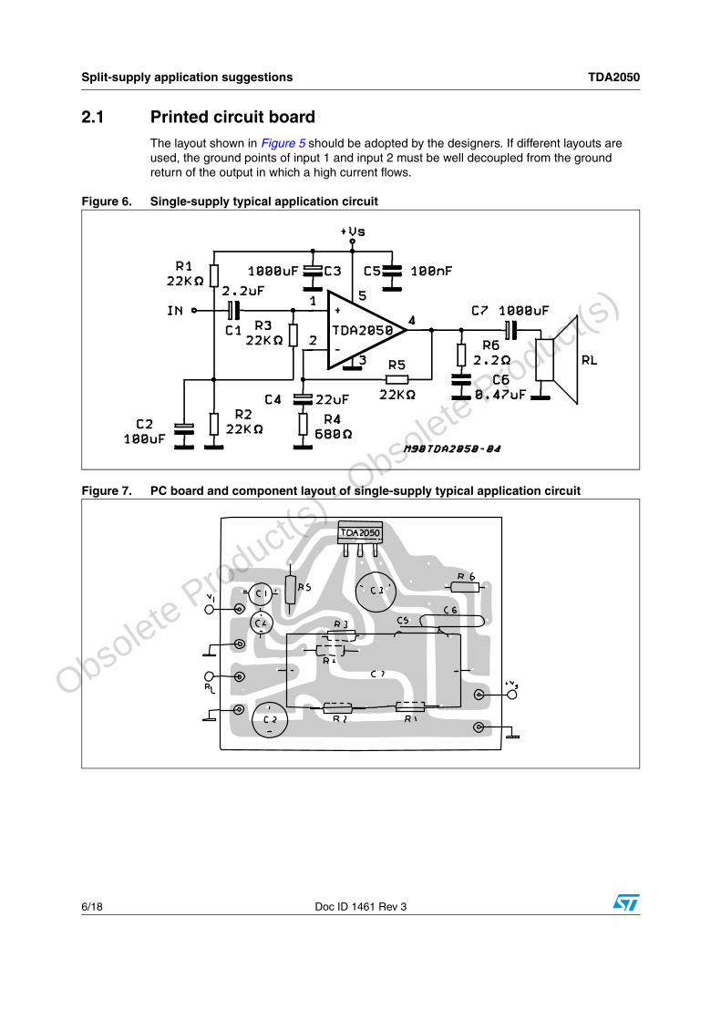
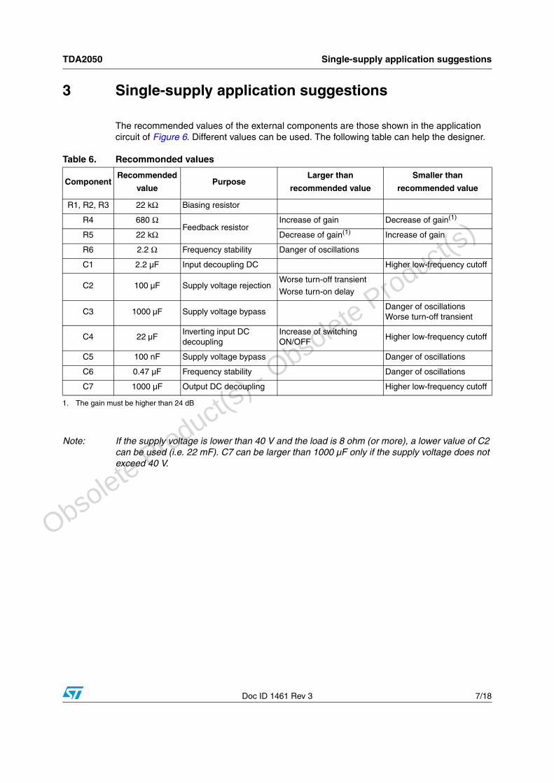
2.1 Printed circuit boardThe layout shown in Figure 5 should be adopted by the designers. If different layouts are used, the ground points of input 1 and input 2 must be well decoupled from the ground return of the output in which a high current flows.
Figure 6. Single-supply typical application circuit
Figure 7. PC board and component layout of single-supply typical application circuit
O
bsolete Product(
s) - O
bsolete Product(
s)
TDA2050 Single-supply application suggestions
Doc ID 1461 Rev 3 7/18
3 Single-supply application suggestions
The recommended values of the external components are those shown in the application circuit of Figure 6. Different values can be used. The following table can help the designer.
Table 6. Recommonded values
Note: If the supply voltage is lower than 40 V and the load is 8 ohm (or more), a lower value of C2 can be used (i.e. 22 mF). C7 can be larger than 1000 µF only if the supply voltage does not exceed 40 V.
ComponentRecommended
valuePurpose
Larger than
recommended value
Smaller than
recommended value
R1, R2, R3 22 kΩ Biasing resistor
R4 680 ΩFeedback resistor
Increase of gain Decrease of gain(1)
1. The gain must be higher than 24 dB
R5 22 kΩ Decrease of gain(1) Increase of gain
R6 2.2 Ω Frequency stability Danger of oscillations
C1 2.2 µF Input decoupling DC Higher low-frequency cutoff
C2 100 µF Supply voltage rejectionWorse turn-off transient
Worse turn-on delay
C3 1000 µF Supply voltage bypassDanger of oscillations Worse turn-off transient
C4 22 µFInverting input DC decoupling
Increase of switching ON/OFF
Higher low-frequency cutoff
C5 100 nF Supply voltage bypass Danger of oscillations
C6 0.47 µF Frequency stability Danger of oscillations
C7 1000 µF Output DC decoupling Higher low-frequency cutoff
O
bsolete Product(
s) - O
bsolete Product(
s)

Typical characteristics (split-supply test circuit unless otherwise specified) TDA2050
8/18 Doc ID 1461 Rev 3
4 Typical characteristics (split-supply test circuit unless otherwise specified)
Figure 8. Output power vs. supply voltage Figure 9. Distortion vs. output power
Figure 10. Output power vs. supply voltage Figure 11. Distortion vs. output power
O
bsolete Product(
s) - O
bsolete Product(
s)

TDA2050 Typical characteristics (split-supply test circuit unless otherwise specified)
Doc ID 1461 Rev 3 9/18
Figure 12. Distortion vs. frequency Figure 13. Distortion vs. frequency
Figure 14. Quiescent current vs. supply voltage
Figure 15. Supply voltage rejection vs. frequency
O
bsolete Product(
s) - O
bsolete Product(
s)

Typical characteristics (split-supply test circuit unless otherwise specified) TDA2050
10/18 Doc ID 1461 Rev 3
Figure 16. Supply voltage rejection vs. frequency (single-supply) for different values of C2 (Figure 6)
Figure 17. Supply voltage rejection vs. frequency (single-supply) for different values of C2 (Figure 6)
Figure 18. Total power dissipation and efficiency vs. output power
Figure 19. Total power dissipation and efficiency vs. output power
O
bsolete Product(
s) - O
bsolete Product(
s)

TDA2050 Short-circuit protection
Doc ID 1461 Rev 3 11/18
5 Short-circuit protection
The TDA2050 has an original circuit which limits the current of the output transistors. The maximum output current is a function of the collector emitter voltage, hence the output transistors work within their safe operating area. This function can therefore be considered as being peak power limiting rather than simple current limiting. It reduces the possibility that the device gets damaged during an accidental short-circuit from AC output to ground.
O
bsolete Product(
s) - O
bsolete Product(
s)

Thermal shutdown TDA2050
12/18 Doc ID 1461 Rev 3
6 Thermal shutdown
The presence of a thermal limiting circuit offers the following advantages:
1. An overload on the output (even if it is permanent), or an above-limit ambient temperature can be easily tolerated since Tj cannot be higher than 150 °C.
2. The heatsink can have a smaller factor of safety compared with that of a conventional circuit. There is no possibility of device damage due to high junction temperature. If for any reason, the junction temperature increases up to 150 °C, the thermal shutdown simply reduces the power dissipation and the current consumption.
The maximum allowable power dissipation depends upon the thermal resistance junction-ambient. Figure 20 shows this dissipable power as a function of ambient temperature for different thermal resistances.
Figure 20. Maximum allowable power dissipation vs. ambient temperature
6.1 Mounting instructionsThe power dissipated in the circuit must be removed by adding an external heatsink. Thanks to the pentawatt package, the heatsink mounting operation is very simple, a screw or a compression spring (clip) being sufficient. Between the heatsink and the package it is better to insert a layer of silicon grease, to optimize the thermal contact; no electrical isolation is needed between the two surfaces. Figure 21 shows an example of a heatsink.
O
bsolete Product(
s) - O
bsolete Product(
s)

TDA2050 Thermal shutdown
Doc ID 1461 Rev 3 13/18
6.2 Dimension recommendationsThe following table shows the length that the heatsink in Figure 21 must have for several values of Ptot and Rth.
Table 7. Dimension recommendations
Figure 21. Example of heatsink
Ptot (W) 12 8 6
Length of heatsink (mm) 60 40 30
Rth of heatsink (°C/W) 4.2 6.2 8.3
O
bsolete Product(
s) - O
bsolete Product(
s)

TDA2050
14/18 Doc ID 1461 Rev 3
Appendix A
A.1 Music power conceptMusic power is (according to the IEC clauses n.268-3 of Jan. 83) the maximum power which the amplifier is capable of producing across the rated load resistance (regardless of non-linearity) 1 sec after the application of a sinusoidal input signal of frequency 1 kHz. According to this definition our method of measurement comprises the following steps:
● Set the voltage supply at the maximum operating value
● Apply a input signal in the form of a 1 kHz tone burst of 1 sec duration: the repetition period of the signal pulses is 60 sec
● The output voltage is measured 1 sec from the start of the pulse
● Increase the input voltage until the output signal shows a THD=10%
● The music power is then V2out /RL, where Vout is the output voltage measured in the
condition of point 4 and RL is the rated load impedance
The target of this method is to avoid excessive dissipation in the amplifier.
A.2 Instantaneous powerAnother power measurement (maximum instantaneous output power) was proposed by the IEC in 1988 (IEC publication 268-3 subclause 19.A). We give here only a brief extract of the concept, and a circuit useful for the measurement. The supply voltage is set at the maximum operating value.
The test signal consists of a sinusoidal signal whose frequency is 20 Hz, to which are added alternate positive and negative pulses of 50 µs duration and 500 Hz repetition rate. The amplitude of the 20 Hz signal is chosen to drive the amplifier to its voltage clipping limits, while the amplitude of the pulses takes the amplifier alternately into its current-overload limits. A circuit for generating the test signal is given in Figure 22.
The load network consists of a 40 µF capacitor, in series with a 1 ohm resistor. The capacitor limits the current due to the 20 Hz signal to a low value, whereas for the short pulses the effective load impedance is of the order of 1 ohm, and a high output current is produced.
Using this signal and load network the measurement may be made without causing excessive dissipation in the amplifier. The dissipation in the 1 ohm resistor is much lower than a rated output power of the amplifier, because the duty-cycle of the high output current is low. By feeding the amplifier output voltage to the Xplates of an oscilloscope, and the voltage across the 1 ohm resistor (representing the output current) to the Y=plates, it is possible to read on the display the value of the maximum instantaneous output power.
The result of this test applied on the TDA2050 is:
Peak power = 100 W typ
O
bsolete Product(
s) - O
bsolete Product(
s)

TDA2050
Doc ID 1461 Rev 3 15/18
Figure 22. Test circuit for peak power measurement
O
bsolete Product(
s) - O
bsolete Product(
s)

Package mechanical data TDA2050
16/18 Doc ID 1461 Rev 3
7 Package mechanical data
Figure 23. Pentawatt V package
In order to meet environmental requirements, ST offers these devices in different grades of ECOPACK® packages, depending on their level of environmental compliance. ECOPACK® specifications, grade definitions and product status are available at: www.st.com. ECOPACK® is an ST trademark.
OUTLINE ANDMECHANICAL DATA
DIM.mm inch
MIN. TYP. MAX. MIN. TYP. MAX.A 4.80 0.188C 1.37 0.054D 2.40 2.80 0.094 0.11D1 1.20 1.35 0.047 0.053E 0.35 0.55 0.014 0.022E1 0.76 1.19 0.030 0.047F 0.80 1.05 0.031 0.041F1 1.00 1.40 0.039 0.055G 3.20 3.40 3.60 0.126 0.134 0.142G1 6.60 6.80 7.00 0.260 0.267 0.275H2 10.40 0.41H3 10.40 0.409L 17.55 17.85 18.15 0.691 0.703 0.715L1 15.55 15.75 15.95 0.612 0.620 0.628L2 21.2 21.4 21.6 0.831 0.843 0.850L3 22.3 22.5 22.7 0.878 0.886 0.894L4 1.29 0.051L5 2.60 3.00 0.102 0.118L6 15.10 15.80 0.594 0.622L7 6.00 6.60 0.236 0.260L9 2.10 2.70 0.083 0.106L10 4.30 4.80 0.170 0.189M 4.23 4.5 4.75 0.167 0.178 0.187M1 3.75 4.0 4.25 0.148 0.157 0.187V4 40° (Typ.)V5 90° (Typ.)DIA 3.65 3.85 0.143 0.151
Pentawatt V
0015981 F
L
L1
A
C
L5
D1L2
L3
E
M1
MD
H3
Dia.
L7
L9
L10
L6
F1H2
F
G G1
E1F
E
V4
RESIN BETWEENLEADS
H2
V5
V4
PENTVME
L4
Weight: 2.00gr
O
bsolete Product(
s) - O
bsolete Product(
s)

TDA2050 Revision history
Doc ID 1461 Rev 3 17/18
8 Revision history
Table 8. Document revision history
Date Revision Changes
31-Aug-2011 3
Removed minimum value from Pentawatt (vertical) package
dimension H3 in Figure 23: Pentawatt V package
Revised general presentation, minor textual updates
O
bsolete Product(
s) - O
bsolete Product(
s)

TDA2050
18/18 Doc ID 1461 Rev 3
Please Read Carefully:
Information in this document is provided solely in connection with ST products. STMicroelectronics NV and its subsidiaries (“ST”) reserve theright to make changes, corrections, modifications or improvements, to this document, and the products and services described herein at anytime, without notice.
All ST products are sold pursuant to ST’s terms and conditions of sale.
Purchasers are solely responsible for the choice, selection and use of the ST products and services described herein, and ST assumes noliability whatsoever relating to the choice, selection or use of the ST products and services described herein.
No license, express or implied, by estoppel or otherwise, to any intellectual property rights is granted under this document. If any part of thisdocument refers to any third party products or services it shall not be deemed a license grant by ST for the use of such third party productsor services, or any intellectual property contained therein or considered as a warranty covering the use in any manner whatsoever of suchthird party products or services or any intellectual property contained therein.
UNLESS OTHERWISE SET FORTH IN ST’S TERMS AND CONDITIONS OF SALE ST DISCLAIMS ANY EXPRESS OR IMPLIEDWARRANTY WITH RESPECT TO THE USE AND/OR SALE OF ST PRODUCTS INCLUDING WITHOUT LIMITATION IMPLIEDWARRANTIES OF MERCHANTABILITY, FITNESS FOR A PARTICULAR PURPOSE (AND THEIR EQUIVALENTS UNDER THE LAWSOF ANY JURISDICTION), OR INFRINGEMENT OF ANY PATENT, COPYRIGHT OR OTHER INTELLECTUAL PROPERTY RIGHT.
UNLESS EXPRESSLY APPROVED IN WRITING BY TWO AUTHORIZED ST REPRESENTATIVES, ST PRODUCTS ARE NOTRECOMMENDED, AUTHORIZED OR WARRANTED FOR USE IN MILITARY, AIR CRAFT, SPACE, LIFE SAVING, OR LIFE SUSTAININGAPPLICATIONS, NOR IN PRODUCTS OR SYSTEMS WHERE FAILURE OR MALFUNCTION MAY RESULT IN PERSONAL INJURY,DEATH, OR SEVERE PROPERTY OR ENVIRONMENTAL DAMAGE. ST PRODUCTS WHICH ARE NOT SPECIFIED AS "AUTOMOTIVEGRADE" MAY ONLY BE USED IN AUTOMOTIVE APPLICATIONS AT USER’S OWN RISK.
Resale of ST products with provisions different from the statements and/or technical features set forth in this document shall immediately voidany warranty granted by ST for the ST product or service described herein and shall not create or extend in any manner whatsoever, anyliability of ST.
ST and the ST logo are trademarks or registered trademarks of ST in various countries.
Information in this document supersedes and replaces all information previously supplied.
The ST logo is a registered trademark of STMicroelectronics. All other names are the property of their respective owners.
© 2011 STMicroelectronics - All rights reserved
STMicroelectronics group of companies
Australia - Belgium - Brazil - Canada - China - Czech Republic - Finland - France - Germany - Hong Kong - India - Israel - Italy - Japan - Malaysia - Malta - Morocco - Philippines - Singapore - Spain - Sweden - Switzerland - United Kingdom - United States of America
www.st.com
O
bsolete Product(
s) - O
bsolete Product(
s)