NYOZ - Not Your Old Z80 · 2 Concept There have been several approaches to designing and building...
65
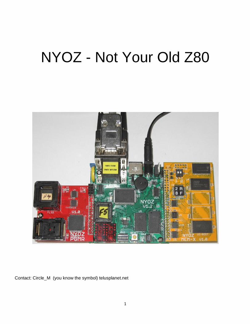
1 NYOZ - Not Your Old Z80 Contact: Circle_M (you know the symbol) telusplanet.net
Transcript of NYOZ - Not Your Old Z80 · 2 Concept There have been several approaches to designing and building...
1
NYOZ - Not Your Old Z80
Contact: Circle_M (you know the symbol) telusplanet.net
2
Concept
There have been several approaches to designing and building Z80 compatible systems in the 21st Century:
- Classic design using classic chips that were available in the 1970's / 80's - Classic design using 74*xx chips with newer (i.e. faster) CPU's, RAMs, etc. - Using newer Zilog devices (Z180, Z280, Z380 & eZ80) with newer support chips - Integration of the Z80 core within an FPGA for higher performance and integration - Emulation on a Personal Computer or other modern fast processor
My primary objective was to create a hardware and software development environment that allowed for designing and testing of new peripheral circuits using a genuine Z8S180 chip at its maximum specified clock rate. Simultaneously, I have tried to identify potential bottlenecks and eliminate them in order to optimize overall performance. There is always more that could be done but so far I'm quite impressed by what is possible. This is definitely not the 2MHz Z80 based S100 system that I built in the mid 1970's! The use of an actual Zilog chip versus an FPGA implementation should guarantee the compatibility and allow for easy porting of peripheral circuit designs to other projects. Since many of the newer support devices (i.e. peripherals, CPLDs, FPGAs, etc.) are based on 3.3V, I also wanted a development platform that provided the required signals for both 5V expansion boards plus a fully translated 3.3V interface. This could have been done by running the CPU at 3.3V but since performance was also a key objective, this mandated 5V for the 33 MHz CPU since the Z8S180 specifications limit it to 20 MHz at 3.3V. Note that throughout these pages I sometimes refer to a Z8S180 and sometimes a Z180. References to the Z8S180 are primarily used when referring to its unique properties whereas Z180 is a more general term covering the common features of this family of chips (i.e. Z8018x, Z8L180 & Z8S18x). The approach I took was to create a base module with stackable side wings on headers; a 5V interface on one side and a 3.3V interface on the other. The 3.3V wings have provisions for memory, I/O and DMA interfaces whereas the 5V wings are only for I/O devices, possibly using the Z180's internal DMA controllers. This makes for a much wider physical system than a vertically stacked design such as PC/104 but it does allow all signals to be easily probed. After all, the original objective was for a development and testing environment. Similarly, the main flash boot chip is socketed to allow for simple updates using commonly available external programmers during early development stages. This also allows for the simple creation and saving of multiple "ROM" revisions. The flash chip could have been soldered in place and programmed via the 3.3V header but that would have required a unique custom programming cable plus it would still require external programmer logic. The base module is fully capable of being a self-contained CP/M or MP/M system without the use of any expansion boards and the peripherals on it are a combination of old-school (i.e. hex LEDs & DIP switch) plus some that I wanted for development purposes. Some of the chips used may not be the cheapest, but the selection criteria was primarily based on performance, functionality and a relatively small board size. Some of the chips and/or packages were also selected as a result of already having a supply of them which lowered the development costs. There is also some extra circuitry and programmable options on the base module and various expansion wings that probably would not be used for a complete system. However, this does create a flexible development environment where software can be developed and tested without requiring physical hardware changes. Would I make some changes if I were starting this project all over? Absolutely! However, the entire process from concept through design to fully tested boards plus software development can take a tremendous amount of time and effort. The boards described herein perform their stated objectives and that was the ultimate goal. Rather than constantly re-working these development boards, I would rather dedicate the majority of further hardware efforts towards designing and building a complete and homogenous system. The software is an ongoing development effort which sometimes reveals simple hardware enhancements that can increase overall system performance. Of course, if actual errors are discovered in these boards then I update them as appropriate. One of the enlightening aspects of designing / building / testing both the hardware (including CPLDs) and software has been to see how the hardware and software work together and to realize how a simple change in one of them can sometimes significantly impact the other to either simplify usage or increase the overall performance of the system. I have a concept for a very small and encased full system based on the Z180. Because the boards described here are primarily for a development system, many of the features that would be on the full system are actually on wings rather than the base module which allows for easy prototyping and testing. For example, the base module only has a
3
RAMdisk, an optional [M]RAM disk and a 512KB 8-bit memory-mapped boot / "read-mostly" flash disk. The optional wings provide the support for physical disk devices such as floppies, CF, SD, [S]ATA, etc. Likewise, additional memory and other interfaces such as USB, video and Ethernet are also on wings. I use the term "read-mostly" to describe some chip-based flash disks such as the implementation of parallel flash on the base module. The reason is simply that the current software does not support wear levelling on the base flash device. Without wear levelling, all writes to the file system directory occur to the same flash sector and thus it will typically wear out the fastest. The directory sector(s) are buffered but that still means there are typically at least two directory sector writes under CP/M when creating a file. Given that the flash devices used have a typical endurance of 100,000 cycles, that means there are typically only 50,000 (or less) file creations or expansions per flash device. Thus the base module's flash disk is best used for storing fully developed programs and relatively constant data whereas temporary files are best placed on a [M]RAM disk where there isn't a cycle limit. The parallel flash on the MEM-X board and serial flash on the IOX board both have static and dynamic wear levelling which will not be implemented for the base module since it is a socketed device and a "ROM" change could corrupt the data.
Approach I considered using non-standard connectors such as M-DINs for the serial ports which would reduce the bulk of the various boards. However, that would require creating custom patch cables versus standard serial cables. I chose to go with D-subs to maintain cable compatibility with some of the old-school devices I have. Likewise, I considered using USB interfaces for the two serial ports on the Z180. It is possible to build a small daughter board that plugs into the D-sub holes and converts them to USB but DE-9 to USB cables are also readily available. Similarly, the wing connectors could have been unique connectors which would reduce bulk and make for easier [dis]connecting. However, standard 0.1" connectors were used since they're readily available and compatible with common 0.1" perfboard for prototyping. These 0.1" connectors were also mounted vertically rather than horizontally which reduces the overall width either with or without wings but it does mean that the first layer of wings are 1/2" higher than the base module. I'm not a big fan of using headers and jumpers to set various options. Sure I have a large supply of them, but they take up board space and someone invariably sets a wrong and possibly damaging configuration. The labelling and/or documentation for jumpers is often minimal and lost through the years. There are only two jumpers on the base module; one to disconnect the clock's backup battery and one to disconnect the optional keyboard interface during programming. When using CPLDs, functions like address decoders and programmable options (i.e. registers) can easily be incorporated within the CPLD which alleviates most of the need for jumpers. It also helps if there is a software configuration utility so that some options are not hardcoded into BIOS routines and incompatibilities in the settings can be checked for and eliminated before saving them. I haven't expanded these concepts nearly to the level of Plug and Play (PnP) but since the CPLDs are reprogrammable, changes such as I/O addresses can be made quite simply and without any physical hardware changes. I also included a DIP switch that can be used by the software to selectively enable / disable features which is very handy during software development. I *HATE* wait states unless absolutely required, especially when using a processor that does not have a separate bus and execution unit. Just a single memory wait state can effectively reduce the overall speed by ~25% (i.e. effectively dropping a 33 MHz CPU down to 25 MHz) and two memory wait states reduce the same 33 MHz CPU to about 20 MHz. Three wait states equate to approximately 17 MHz. Leaving the Z180's refresh function active when using static RAM is also a total waste of processor cycles. Unfortunately, some wait states are required for a reasonable price / performance trade-off such as on parallel flash chips and peripherals like the W5100 Ethernet interface. By incorporating an intelligent wait state generator into the base module's CPLD, these wait states only need to be inserted where absolutely necessary versus using the Z180's DMA/WAIT control register settings which affect all memory and/or I/O accesses. Wait State Testing:
While the above was written as theoretical effects of wait states, I chose to actually test it using ART.BAS. Times were recorded with a stopwatch so they’re only within ½ second or so. At 0 wait states this program took 30 seconds whereas at 1 wait state it took 40 seconds. Two and three wait states 49 and 59 seconds respectively. Thus the above theoretical MHz reduction numbers prove to be accurate in practice.

4
Just like wait states, I've found that the speed of peripherals makes a huge difference on the perceived speed of a system. Programs can be either compute bound or I/O bound and I've generally found them to be I/O bound for many of the tasks I perform. Going from 9600 baud to 115,200 with a fast serial terminal (or emulator) makes the user feel like the system is supercharged when displaying a full screen. A full screen at 24x80 and 9600 baud takes a minimum of 2 seconds for an 8-N-1 serial transfer and that doesn't include any interrupt or polling delays if the UART isn't buffered. At 115,200 the protocol delay is only 1/6 of a second and the perceived speed will be 12 times faster even though there is absolutely no difference in the number of processor cycles required. This speed difference is much more apparent when comparing XMODEM and 1K-XMODEM over a serial port versus a USB port ... elapsed times for a 700KB file transfer ranged from ~14.5 MINUTES for RS-232 at 9600 baud down to 8 SECONDS via USB! That is more than a hundred fold difference in elapsed time!!! At first glance, one may think that polled I/O is suitable for a single user system such as CP/M. Certainly that is true for I/O operations like disk reads where the calling program can't continue until the data is available. However, for things like console output or printer output it makes much more sense to be interrupt driven so the process generating data can continue using the CPU while the interrupt routine worries about when the peripheral can actually accept new data. I chose to make all my BIOS I/O routines interrupt driven which greatly increases the ease of migrating to a multi -user or multi-processing operating system such as MP/M. The byte-oriented I/O routines all have their own FIFO buffers while the block I/O routines can easily accommodate a dispatcher call while waiting for physical I/O. Furthermore, the I/O routines for physical disks all use buffer pools to reduce actual I/O operations such as directory reads. A side benefit of using interrupt driven I/O is that the overall power consumption and heat can be reduced by using the sleep (SLP) instruction. The use of memory-based disks versus Compact Flash (CF) or SD cards is noticeable but either is vastly superior to the use of floppy disks. Also, the use of physical hard drives with their inherent rotational delays is noticeably slower compared to CF/SD cards. Physical hard drive performance can also be dependent upon the host controller and the drive controller with its buffering algorithms ... rotational speed and transfer speeds aren't the only performance factors. This interface and controller dependency is also true for CF/SD cards, especially for writes. My preference is to use memory-based "disks" whenever possible and a good example is the SLVRAMD utility: analyzing 316KB of RAMdisk data and writing back to RAMdisk a 275KB image of valid data took well under one second. Although I've designed and done some testing on a floppy disk interface, I have no idea how much longer this imaging task would have taken using a floppy disk ... most certainly a lot longer. I rarely have that interface connected and I avoid the use of floppy disks
whenever possible since they're extremely slow and physically bulky. The reason I went with custom 16-bit DMA controllers for memory-to-memory and block I/O devices is simply performance. They add a bit of extra monetary cost and certainly a lot of extra development overhead, but the results are very significant. The Z180 block I/O commands (INIR/OTIR) take 14*Tcyc (420ns per byte @ 33MHz) for an effective transfer rate of ~2.38 MB/sec. Utilizing the Z180 DMA controller can halve the time to 7*Tcyc (210 ns/byte) or effectively ~4.76 MB/sec. The custom DMA controller can effectively transfer data 28 times faster at ~133 MB/sec or UDMA 6 rate!!! That's not quite the UDMA 7 rate of 167 MB/s but that could probably be obtained with some extra development effort. The I/O device, such as a CF or SD card, usually becomes the limiting factor on the transfer rate now, rather than the interface on the data path from the device to main RAM. Besides 8-bit versus 16-bit, another advantage of custom DMA controllers is they can allow for the use of a fly-by technique. Most DMA controllers first read the source data into a temporary register then write it out to the destination and thus take two bus cycles. However, it is possible for an I/O device to directly interface to memory without the intermediate buffer and thus use only one bus cycle. Only one device (memory or I/O) can use the main addressing lines while each device requires separate chip selects. Another potential problem is with the use of the read / write signals. Only one device can use the main read / write signals and the other device needs to rely upon either the chip select or a unique read / write signal to determine direction. The NYOZ boards let memory use the main signals while certain I/O devices use unique selects and addressing for DMA operations. Historically one thinks of a parallel memory device to be the fastest implementation of a RAM or ROM disk. With the advent of some of the newer serial devices, this is not always true. Even using a custom DMA controller, a large parallel flash device can take 70+ns to read and 10+ns to write to RAM ... effectively about 90+ns per transfer when one adds in some extra time for the controller or about 45ns / byte using a 16-bit bus. Even using separate data busses and buffering, the flash device still restricts transfer speed to about 40ns per byte or word. Some of the newer commonly available serial flash devices can transfer a nibble at 7.5ns or 15ns per byte. Since the two nibble reads can't use the main data bus directly, a 4-bit latch and two reads are required. A unique DMA controller can handle the nibble issue while overlapping flash / RAM operations and thus the speed limitation is simply the slower of the flash device or memory.
5
Theoretically one can transfer data about three times as fast from the serial vs. parallel device and it is also physically smaller when excluding the controller. The NYOZ XIO board demonstrates how serial devices can be further enhanced to produce a 7.5ns per byte (133 MB/s) read interface and further CPLD development could make it even faster. However, since it is flash based the writes are much slower with a maximum of ~1.5us per byte (~673KB/s) to completion but excluding an erase. For reference, on my main PC a 200MB copy from SSD to a new Sandisk Cruzer Glide 32GB thumbdrive via USB 2.0 ended at a data rate of just over 900 KB/s although a ~10GB copy to an identical used device was consistently about 3.25 MB/s. I assume that some of the difference is in the number of small files which cause a lot of directory re-writing. Update:
There are now much faster parallel flash devices available (i.e. Micron's G18) but they're expensive and only available in BGA packaging. Note that the serial flash devices are already considerably cheaper than their equivalent capacity (but slower speed) parallel devices. Likewise the Cypress S26KL series of 8-bit clocked devices would be very interesting to play with if it wasn't for the fact they're only available in BGA packages.
I no longer have any serial peripherals that use anything other than asynchronous protocols. As a result, I have not designed any NYOZ-family boards to use USARTs such as the SIO or SCC that support bisynchronous, HDLC, SDLC etc. The base module's serial ports only support RTS/CTS handshaking while the serial ports on the FDC board support a full complement of RS-232 modem signals the same as a PC. I included RS-485 support on the base module's ASCI 1 port and also on the MPZ4 board to allow for the development of software protocols that would easily allow for devices to be distributed over relatively long distances (up to 4,000 feet). I am aware that many end users and even some designers choose to either over-clock devices or violate timing limitations. That is their choice and it may work under certain conditions but I choose to never consciously do so. Although it may require more expensive devices, extra support circuitry or even wait states, I believe that manufacturers have specified their timing restrictions for a good reason, whether that be to cover the full temperature range and manufacturing variations or some other condition. Violating these limits can expose the system to unusual or one-time glitches that may be extremely difficult to diagnose or possibly it may corrupt data in very subtle ways. I am not aware of any timing violations in my boards when populated with the specified devices and using the supplied software. All memory and I/O timings have been carefully checked. With that being said, there may be a potential for timing issues if multiple boards are stacked on the wings which will increase the capacitance and delays of various signals (i.e. rise / fall times). Correction:
Upon reviewing the datasheets for TIL-311 hex displays and various pin-compatible substitutes, they list the data setup time as 50ns and a hold time of 40ns which is longer than the Z8S180's theoretical minimum data output time of 70ns. I have never had any issue with these devices as implemented here or when used in other similar designs. Based on implementation experience with these displays, it would appear that the hold time is more critical than the setup time. At this time I have not done further investigation as to whether these specifications are overly conservative or there is some other factor at play.
Sidenote:
It was interesting to note the actual vs. theoretical timing during the verification of the wait state generator. The Zilog datasheet only specifies the maximum delay for signal transitions from clock edges but not the minimum. Theoretically the MREQ* signal could be as short as ~32ns for reads and about 15ns less (~17ns) for op-code reads. In reality, on the oscilloscope I used, this signal was ~59ns. Regardless, I used the theoretical timing for compatibility reasons since this was only verified on a couple of older mask versions of the Z8S180.
Just like over-clocking, I'm aware that some computer users choose to mix-and-match or use a "just try it" approach when adding chips and/or peripherals. In contrast, I try to actually understand the design requirements and function(s) of these devices before including them in a project, especially one with public documentation. That understanding also includes a careful look at all the timing requirements. In other words, I prefer to actually try engineer my designs rather than just slap a bunch of parts together in the hope that it may work under some set of circumstances. Ideally a design should work across all the various variables, including different revisions of the specified chips, the full temperature range, clock range, etc. I'm certainly not claiming my designs are perfect, but I do try to carefully review the various datasheets and adhere to them. I actually designed several different variants of the base module. Functionally, they're basically all identical with the main difference being the type of CPLD used and the wait state generation. At 33 MHz, the most difficult system timing is in the memory wait state logic where there is only a 5ns worst-case window from the MREQ* signal going active
6
to when external support logic must drive the WAIT* signal active. The fastest version of the original CPLD was only 6ns and thus was in violation of this window. It required wait states to be set via the Z180's DMA/WAIT control register which then affected all memory accesses. A redesign of the base module using a completely different and faster CPLD met this timing restriction but at a significantly higher monetary price (~$11 difference in low volume but I did find a source for the original CPLD at more than $20 cheaper than the faster one). By modifying the layout and logic in the base module with the original CPLD plus using a single external gate (less than $0.50), it was possible to actually incorporate the intelligent wait state generator within the lower cost CPLD, albeit it did require a PCB revision from V1.0 to V1.1. The design with the faster and more expensive CPLD was never fabricated. Another timing area that one must pay careful attention to is the reading of parallel flash devices. Most of these devices have a relatively slow output to float delay (i.e. 20ns) and although the CE* and OE* signals have both gone inactive the device may continue to drive the data bus. This requires careful timing analysis of subsequent bus cycles. The current CPLD handles this but alternate designs may need to use a discrete tri-state buffer to eliminate this potential problem. Since the Z180 signals are essentially asynchronous to CPLDs and FPGAs, one has to pay careful attention to their timing. Even the simpler CPLD logic functions have a potential "gotcha" that can occur when modifying them. The fitter and optimizer can sometimes add or remove levels of logic from previous iterations and this can lead to unexpected timing violations. It has been my experience that when making changes to a CPLD with tight timing but no timing constraint file, I always review the final equations and check to see whether extra layers of logic have been added or removed. Logic level changes may require manual intervention and a re-fit / re-optimize. DISCLAIMER:
Some of the timings that are described in these pages for custom DMA controllers are based on the future full system and not the development system described herein. The issue is that in the full system a single CPLD or FPGA can contain both the memory decoder / selector and the DMA controllers whereas in this development system there are multiple separate CPLDs on different boards. Thus when a DMA controller on a wing does a memory access, there is a delay before the memory decoder / selector in the base module's CPLD actually asserts the appropriate memory chip select. In a single homogenous CPLD or FPGA these events can occur simultaneously whereas in this development system the delay must be compensated for.
Z8S180 Undocumented ERRATA ?
1) This occurred on a 2000 KN revision Z8S180 but I haven't done further testing on other revisions. The Z180 User Manual clearly states that the ASCI BRG high and low registers are initialized to zero at reset which was verified by reading them prior to any writes. Since only the low register needs to be changed for rates of 4800 and above, the ASCI 0 BRG high register (ASTC0H) was not written ... this resulted in no communication. The only change to the code was to write 00 to this register and communication worked properly and exactly as expected. Until this anomaly is fully understood, the solution is to always initialize (i.e. write) both the BRG high and low registers (ASTC0H / ASTC0L and ASTC1H / ASTC1L) when using the BRG feature.
2) The Z8S180's clock generator has the option of using an input frequency (crystal or oscillator) with a value of 2x,
1x or 1/2 of the desired PHI frequency and the selection is controlled by the CCR (CPU Control) and the CMR (Clock Multiplier) Registers. However, the CMR register *must* be written to before the CCR register when using an input frequency that is 1/2 the desired PHI frequency. This has been verified on different mask revisions and with both crystal and oscillator inputs.
3) As noted in the description of the MPZ4 board, I have detected an issue with the SLP (sleep) instruction when used on a Z8S180 with an oscillator input versus a crystal. Further investigation is required as to whether this is just on certain mask versions or a general problem. For now, SLP works as expected on all my various base modules which use a crystal while MPZ4 boards which use an oscillator should use the HALT instruction.
7
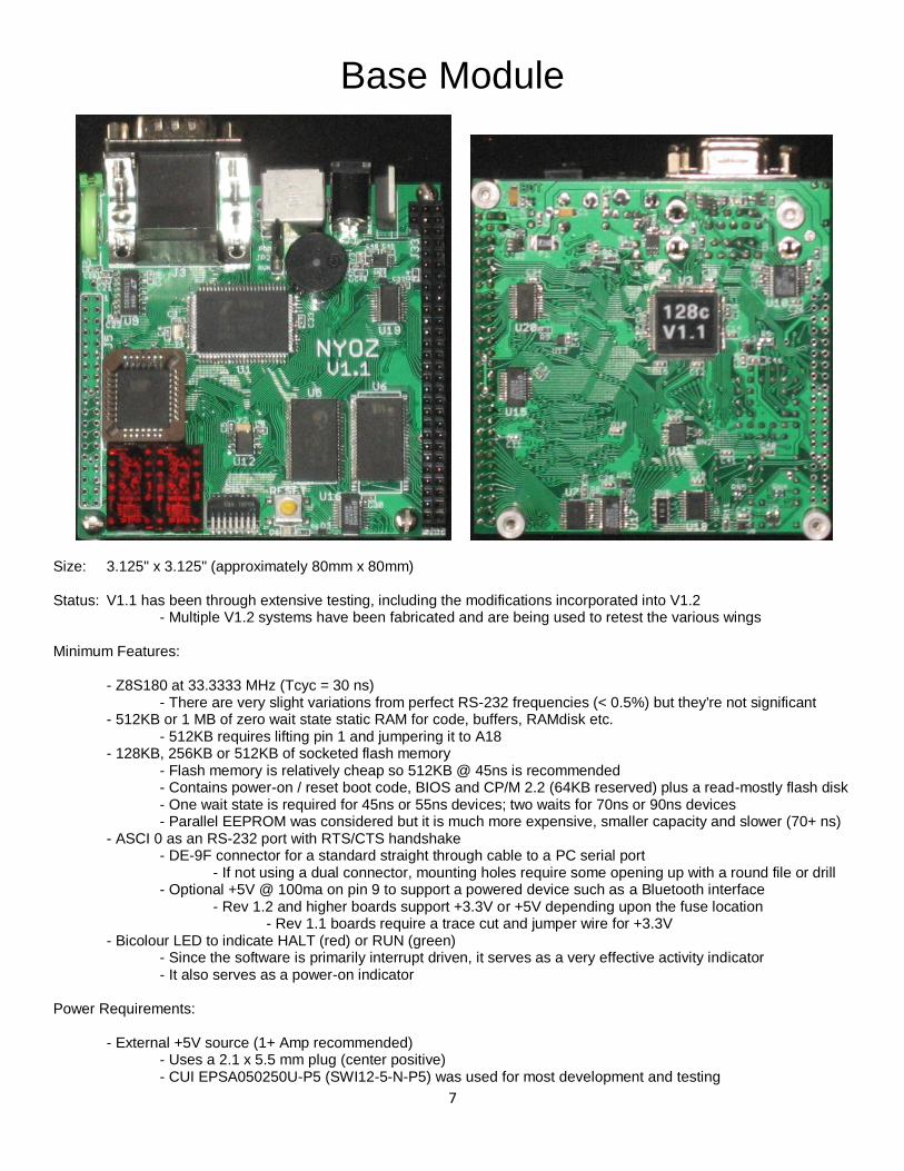
Base Module
Size: 3.125" x 3.125" (approximately 80mm x 80mm) Status: V1.1 has been through extensive testing, including the modifications incorporated into V1.2 - Multiple V1.2 systems have been fabricated and are being used to retest the various wings Minimum Features: - Z8S180 at 33.3333 MHz (Tcyc = 30 ns) - There are very slight variations from perfect RS-232 frequencies (< 0.5%) but they're not significant - 512KB or 1 MB of zero wait state static RAM for code, buffers, RAMdisk etc. - 512KB requires lifting pin 1 and jumpering it to A18 - 128KB, 256KB or 512KB of socketed flash memory - Flash memory is relatively cheap so 512KB @ 45ns is recommended - Contains power-on / reset boot code, BIOS and CP/M 2.2 (64KB reserved) plus a read-mostly flash disk - One wait state is required for 45ns or 55ns devices; two waits for 70ns or 90ns devices - Parallel EEPROM was considered but it is much more expensive, smaller capacity and slower (70+ ns) - ASCI 0 as an RS-232 port with RTS/CTS handshake - DE-9F connector for a standard straight through cable to a PC serial port - If not using a dual connector, mounting holes require some opening up with a round file or drill - Optional +5V @ 100ma on pin 9 to support a powered device such as a Bluetooth interface - Rev 1.2 and higher boards support +3.3V or +5V depending upon the fuse location - Rev 1.1 boards require a trace cut and jumper wire for +3.3V - Bicolour LED to indicate HALT (red) or RUN (green) - Since the software is primarily interrupt driven, it serves as a very effective activity indicator - It also serves as a power-on indicator Power Requirements: - External +5V source (1+ Amp recommended) - Uses a 2.1 x 5.5 mm plug (center positive) - CUI EPSA050250U-P5 (SWI12-5-N-P5) was used for most development and testing

8
Optional Features: - ASCI 1 as a selectable RS-232 (with RTS/CTS) or RS-422/485 full/half duplex port - DE-9M connector - RS-232 versus RS-422/485 and full/half duplex is set via the cable wiring - A standard null modem cable allows direct connection to a PC serial port ##need to verify## - Two TIL311, HTIL311* or INL0397-1 LED's for a hex display port - Decimal point LEDs are individually software settable which creates four unique ON/OFF LEDs - INL0397-1 uses considerably less power but are very hard to obtain
- HTIL311* uses more power than INL3097-1 but less than TIL311's - 8 position DIP switch - Buzzer - I2C interface - 3.3V header adjacent to the 3.3V expansion header
- Currently just a simple bit-bang interface since it's only used once during initialization and by configuration utilities
- Future enhancements may add an I2C controller into the CPLD - I2C EEPROM
- 24C0x (128|256|512 byte) or AT24MAC[4|6]02 (256 byte EEPROM, 16 byte serial number, 4|6 byte EUI address)
- I2C battery-backed real time clock(s) - PCF8593 and/or MCP7941x (64 bytes RAM, 128 byte EEPROM, [4|6 byte EUI address]) - Both can be installed for software development with default selected by CONFIG.COM - Lithium battery with a disconnect jumper - 1 year worst case, 5+ years typical with both clocks installed - PC-AT Keyboard port via CSI/O port and a PIC12F509 for key scan decoding - Supports CTL-ALT-DEL hardware reset of base module - Currently disabled since more PIC software development is required - 512KB, 1MB or 2MB "disk" - Non-volatile MRAM at 0 wait states - MR2A16A (512KB) or MR4A16B (2MB)
- MR0A16A (128KB) can be used but requires lifting pins 1, 26, 27 & 44 then installing short jumpers
- Requires 1 wait state if instructions being executed directly from MRAM - Direct code execution may not be available on future systems so it is not recommended
- Can also be a CY7C1041V33 (or AS7C34098A-xxTx) for an additional 512KB of RAM / RAMdisk or a CY7C1051DV33 (or AS7C38098A-10TIN) for an additional 1 MB of RAM / RAMdisk
- Pin 28 of a 1 MB RAM device needs to be lifted and connected to PCB Pin 53 - N.B. The wear-levelling algorithms for serial flash on the XIO board rely upon this device as non-volatile memory. With volatile memory the serial flash data would need to be restored from a checkpoint at power-on and might not be accurate and/or reflect changes made since the last checkpoint.
- Low power SRAM such as the CY62157EV30 with a supercap or battery backup was also considered and rejected
- Requires 1 wait state - Supercap of reasonable size would be measured in hours/days, not months/years - Small lithium cell would give months of backup but require extra circuitry and replacement - nvSRAM such as the CY14B1[04|08|16]N was considered, but it is much more expensive than MRAM - F-RAM (i.e. FM22L16) was also considered as an option - More expensive than MRAM at the time of design (nearly 50% more) - Slower than MRAM and requires at least 1 wait state - Much more difficult (and slower) to optimize access via a custom DMA channel - Basic 5V I/O expansion connector (2 x 19 x 0.1") - 8 address lines, 8-bit data and an I/O chip select (16 addresses) - Signals required for I/O, both Z180 internal DMA controllers, interrupts, etc. - Five pins at one end are dedicated for the CPLD's JTAG interface - Enhanced 3.3V expansion connector (2 x 28 x 0.1") - All required control signals for I/O and memory access - 16-bit data bus and all 20 address lines - Support signals for custom DMA controllers

9
- A decoded I/O chip select signal (16 addresses) - A 512KB EXTernal memory select signal There are two notable differences in this base module compared to many other Z80 / Z180 designs. The first one is the use of level translators to allow for both 5V and 3.3V support devices. The second is that the SRAM and MRAM are 16-bit devices which are supported as such on the 3.3V expansion header. There is no software difference to the programmer as a result of the wider devices and the entire contents of each device are accessible via banking and shadowing. The primary advantage of using the wide devices is on the 3.3V wings where DMA controllers (I/O or memory-to-memory) can utilize the increased bus width to reduce the number of required bus cycles and thus increase performance. Software using these wing-based 16-bit DMA controllers must currently ensure that their buffers are aligned on an even address. INT0 Mode 2 interrupts can be received from either the 5V wings or from the 3.3V wings. In order to properly handle this, the base module has a selector based on the side that it first detects an interrupt request on. Rather than just decoding M1* + IORQ* to indicate a Mode 2 interrupt acknowledge, the wings must also include their respective INT_ENABLE* in order to prevent simultaneous acknowledges (i.e. M1* & IORQ* & INT_ENABLE*). Note that on either expansion header if multiple wings on the same header utilize interrupts then these boards must support INT_ENABLE* daisy chaining amongst themselves. Similarly, on the 3.3V wing there is only one BUSACK* signal from the base module and if multiple boards have DMA controllers utilizing this signal they must support BUSACK* daisy chaining. All of the 3.3V wings described in this document support these functions as required but they will require some additional short jumpers for implementation. Currently, the available 5V wings using interrupts do not have support for daisy chaining. Like most things in a system design there are tradeoffs and I generally choose to take the alternative that provides the best overall system performance. Due to the inherent design of the Z8S180's baud rate generators, a system frequency of 29.4912 MHz would have allowed for the serial ports (ASCI0 and ASCI1) to use exact baud rates and also be configured for 230,400 and 460,800 baud. Likewise for 36.864 MHz but that would require a 10.6% overclock using an 18.432 crystal in 2x clock mode. Using a system frequency of 33.3333 MHz limits the maximum standard baud rate to 115,200 with only very minor deviations from the exact baud rates (less than 0.5%) and I have had absolutely no issues communicating with a PC at various rates up to and including 115,200. Higher non-standard baud rates are possible but not usually practical unless only interfacing to other Z8S180 systems. Since serial communication is only one small aspect of the overall system, I chose to use 33.3333 MHz as the system frequency which gives about a 13% improvement in instruction execution speed compared to 29.4912 MHz. One should also note that while most RS-232 serial transceivers will support 120kbps, higher speeds may require going to newer and often more expensive devices. Like the Z8S180 frequency described above, the UARTs on the Super I/O board are also limited to 115,200 baud by their very design. If the user really wants or needs higher speed serial communication they can use the USB ports on the XIO board at rates capable of transferring 8 MBytes/sec and possibly 40 MBytes/sec with further CPLD development. If a board is being built that does not initially include a [M]RAM device for U6, the header for the 3.3V wing should also be left off unless absolutely required. The issue is with hand soldering U6 which would be much more difficult with the header installed. Without the header it is relatively straightforward to solder and check it. This board was originally designed and tested using 1MB SRAM plus 512KB of MRAM and a design decision was made to connect A18 to the MRAM A0 input and A19 to the RAM’s A0. Although this meant A1-A17 (A1-A18 for RAM) were the same for the CPU and SRAM / MRAM, it created an issue when going to smaller devices. The following changes have been tested: For 512KB SRAM, lift pin 1 and connect it to A18 (pin 28 which is a N/C). For 128KB MRAM (MR0A16) four pins need to be lifted and jumpered: Pin 1 -> A14, Pin 26 -> GND, Pin 27 -> +3.3V and pin 44 -> A13. This board uses a 1.5A low dropout linear regulator to step down the 5V input to 3.3V. This provides a LOT more current than required by this board but it was chosen to allow for possible future development of 3.3V wings that may require a lot of current. Another advantage is that at this time there has been no requirement for a heatsink when running the base module along with the currently developed wings since the regulator's tab is barely above ambient temperature. If a high current 3.3V wing is attached then the regulator temperature should be checked and it may be necessary to add a heatsink. The V1.0 board used a 1Amp LM3940 regulator which has the same pinout as some of the more expensive step-down switching regulators whereas the V1.1+ boards use the 1.5A regulator with a different footprint. If there is a need for more than 1.5A of 3.3V current or too much heat dissipation then a revised board with the original pinout may need to be developed in order to use a switching regulator.
10
Note that the lithium battery for the clocks (CR1632V or BR1632V) is directly soldered onto the board. If the user is planning a very long period of non-usage then it may be appropriate to remove the battery jumper which will extend its lifetime. To change the battery, one needs to first remove the jumper then carefully clip off both legs followed by solder removal of the two legs. When installing the new battery, be careful not to allow the one leg to be in contact with the D-sub connector mount ... it is quite close and I choose to also add a small piece of heatshrink on this leg. After soldering the new battery, re-install the jumper and then run either TOD or TIME and DATE to set the clock. The current software uses a dedicated 4KB physical sector buffer in banked RAM for the directory of the base module’s flash "ROM" disk which slightly speeds up access (zero vs. one wait state) and also negates the need to allocate a buffer for directory updates. If MRAM is installed, it is relatively straightforward to place this buffer in non-volatile MRAM and avoid the need to erase and re-write the 4KB directory block on every update. This code has NOT been implemented for two reasons: 1) There should be relatively few writes to this flash device on the development system; 2) The directory could easily get corrupted when using different flash devices in the socket. This will not be a restriction on the full system where a larger flash device is soldered in place as is any MRAM device. In order to minimize the space requirement, I used a half-size DIP switch which works but is not nearly as convenient to use as the full size versions. On the first two boards I used the type with extended side levers but I broke one of the tiny levers when I was being a bit too ham-fisted. I've since changed to the top flush actuator style with the same footprint but they are also a bit inconvenient to use. I would recommend that any software using this switch does not expect regular changes and I only use it for very occasional purposes such as forcing the boot of a very basic system and/or setting the console's baud rate. Note that the logical ON/OFF position of these two types of switches are reversed and the use of a noninverting (side) or inverting (top) buffer/driver is dependent upon which type of switch is used. RTC Software Notes:
This board has the option for two different real-time clocks and their corresponding EEPROMs which allows for the software development and testing of the two different architectures. The choice of primary clock / EEPROM is configurable and that selection also defines which clock generates the once-per-second interrupt. In order to maintain consistency, the configuration and clock setting routines always try to update both of the clocks and EEPROMs. During initialization, if the default EEPROM is not accessible then the other one is accessed and becomes the new default along with its corresponding clock. Thus just one of the clocks and EEPROMs need to be installed but if both are installed the utilities attempt to make them consistent. It should be noted that the PCF clock requires an external EEPROM whereas the MCP device has it incorporated into the basic device. The only functional difference beyond the driver software is the Ethernet MAC address which is uniquely tied to the selected primary clock / EEPROM. Unless changed by the CONFIG utility, the power-on default real-time clock is the PCF clock. To temporarily force the selection of the default real-time clock, this can be done either with the MONitor ( O F0 [00=PCF | 40=MCP] ) or via software doing an OUT (INIT@),[00 | INIT.CLK] and this change will be preserved across RESETs until the next power-on. The future full system is currently planned to use an MCP79521 real-time clock since it is more integrated and lowers the unique device count. Note that by default the clock chips have not been trimmed for accuracy and there may be significant drift. Daylight savings time is automatically checked for and adjusted during RESET. However the normal clock data that is available to programs via subroutine calls is simply a once-per-second interrupt driven software clock which is initialized from the real-time clock during RESET. If the system remains powered on across a daylight savings time change this software clock will not be adjusted and the user will either have to set the time using the TIME / TOD utilities or simply perform a RESET using the pushbutton. A possible future enhancement will be to set an alarm interrupt for the next daylight savings time change or to always re-synchronize the clocks at 2:00 AM which would also compensate for any missed interrupts.
An MRAM "disk" is formatted during the initial testing of a new base module with an MRAM device. It is not anticipated that it should be necessary to subsequently re-format it since a simple ERA *.* should delete all files. However, in the unanticipated event that the MRAM disk becomes unusable, it can be hard formatted using the MONitor and the following sequence of commands: O F1 2 B 10 F 0 FFF E5

11
Significant functional differences in board revision levels - N.B. R0, R10, C9 & U7 not installed or required V1.0 - First PCB for validation purposes V1.1 - Support for intelligent wait states and 3.3V regulator changed from a 1A to 1.5A with different pinout V1.2 - Reduced data bus loading and changed / added some pull-up resistors for better wing compatibility - Allows +3.3V or +5V on ASCI0 DE-9 (female) depending on fuse location
V1.3 - Add labels to left four switches for default functions Base Module I/O connectors: ASCI 0 - DE-9F : 1 - N/C 2 - Tx - Output 3 - Rx - Input 4 - N/C 5 - Ground 6 - N/C 7 - CTS - Input 8 - RTS - Output 9 - Optional +3.3V or +5 @ 100ma Output ASCI 1 - DE-9M : RS-232 RS-485 Full Duplex RS-485 1/2 Duplex 1 - N/C N/C N/C 2 - Rx - Input A |-------- A 3 - Tx - Output B | |---- B 4 - N/C N/C | | Ground --| 5 - Ground |--- Ground | | Ground --| 6 - N/C | N/C | | N/C | 7 - RTS - Output | Z | |---- Z | 8 - CTS - Input | Y |-------- Y | 9 - N/C |--- Ground Ground --| N.B. The dashed lines in the RS-485 configurations above represent connections that must be made within the connector to properly configure the port. There are no RS-485 termination resistors on the actual base module and if these are required, they should also be installed in the connector. MDIN-6: 1 - Keyboard Data [ICSPD] 2 - N/C 3 - Ground 4 - +5V @ 500ma 5 - Keyboard Clock [ICSPC] 6 - N/C or [MCLR* - PIC programming] depending on Jumper
Wing Connectors
Although there are several wings that have already been designed and tested, new wings may be developed either through actual PCB fabrication or via prototyping on perfboard. The following connectors are standard 0.1" headers which allow for easy prototyping. It should be noted that if new wings are developed, they should be aware of the possible need to daisy-chain the INT_ENABLE* and/or BUSACK* signals. New boards should also pay attention to the possible need (actually recommended) to add a physical support post. Using the supplied connectors, a bottom tier wing uses a 3/4" support post and an inter-board support post is 0.437".

12
J5 - 5V Expansion header:
JTAG-TMS 2 1 JTAG-TDI JTAG-TDO 4 3 JTAG-TCK Ground 6 5 +5V RESET* 8 7 JTAG-Port_Enable DREQ0* (open drain) 10 9 TEND0* INT_ENABLE* (Note 1) 12 11 DREQ1* (open drain)
INT_REQUEST* (open drain) 14 13 TEND1* PHI 16 15 CS5* (Note 2) WAIT* (Note 3) 18 17 IORQ* M1* 20 19 ST WR* 22 21 RD* A7 24 23 A6 A5 26 25 A4 A3 28 27 A2 A1 30 29 A0 D1 32 31 D0 D3 34 33 D2 D5 36 35 D4 D7 38 37 D6 Note 1: Mode 2 vector = INT_ENABLE* & IORQ* & M1* Note 2: Decoded Chip Select for sixteen I/O addresses (i.e. x0h:xFh)
~ 62.5ns + nwait*30 for writes and for reads with IOC=0, ~77.5ns + nwait*30 for reads with IOC=1
Note 3: Usage of WAIT* requires a base module jumper and inhibits other base features. NOT recommended!
13
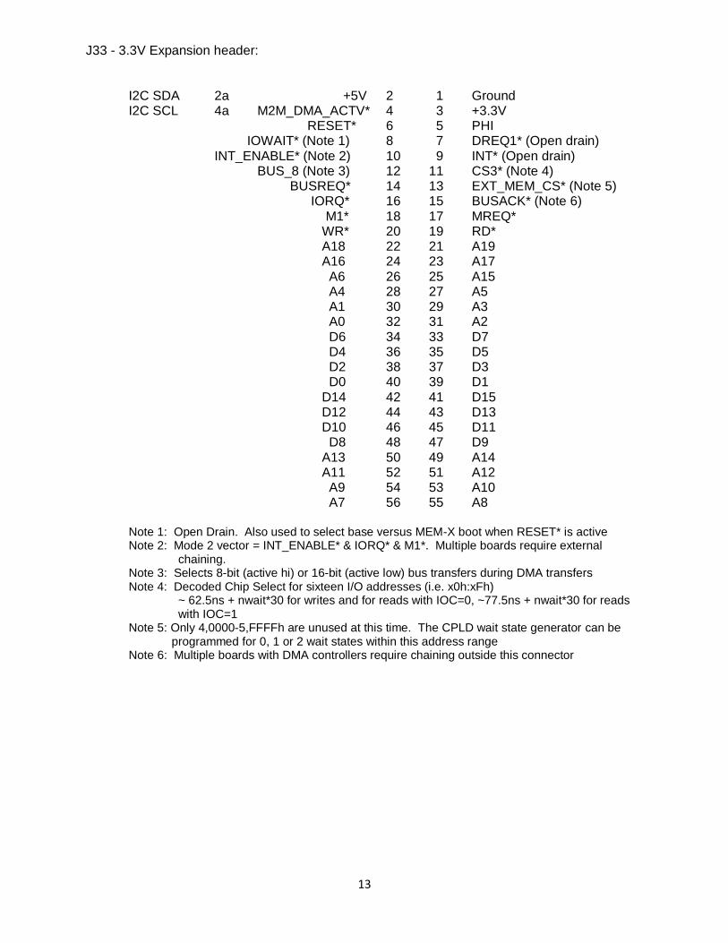
J33 - 3.3V Expansion header:
I2C SDA 2a +5V 2 1 Ground I2C SCL 4a M2M_DMA_ACTV* 4 3 +3.3V RESET* 6 5 PHI IOWAIT* (Note 1) 8 7 DREQ1* (Open drain) INT_ENABLE* (Note 2) 10 9 INT* (Open drain) BUS_8 (Note 3) 12 11 CS3* (Note 4) BUSREQ* 14 13 EXT_MEM_CS* (Note 5) IORQ* 16 15 BUSACK* (Note 6) M1* 18 17 MREQ* WR* 20 19 RD* A18 22 21 A19 A16 24 23 A17 A6 26 25 A15 A4 28 27 A5 A1 30 29 A3 A0 32 31 A2 D6 34 33 D7 D4 36 35 D5 D2 38 37 D3 D0 40 39 D1 D14 42 41 D15 D12 44 43 D13 D10 46 45 D11 D8 48 47 D9 A13 50 49 A14 A11 52 51 A12 A9 54 53 A10 A7 56 55 A8 Note 1: Open Drain. Also used to select base versus MEM-X boot when RESET* is active Note 2: Mode 2 vector = INT_ENABLE* & IORQ* & M1*. Multiple boards require external chaining. Note 3: Selects 8-bit (active hi) or 16-bit (active low) bus transfers during DMA transfers Note 4: Decoded Chip Select for sixteen I/O addresses (i.e. x0h:xFh) ~ 62.5ns + nwait*30 for writes and for reads with IOC=0, ~77.5ns + nwait*30 for reads with IOC=1
Note 5: Only 4,0000-5,FFFFh are unused at this time. The CPLD wait state generator can be programmed for 0, 1 or 2 wait states within this address range
Note 6: Multiple boards with DMA controllers require chaining outside this connector
14
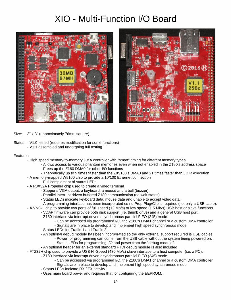
XIO - Multi-Function I/O Board
Size: 3" x 3" (approximately 76mm square) Status: - V1.0 tested (requires modification for some functions) - V1.1 assembled and undergoing full testing Features: - High speed memory-to-memory DMA controller with "smart" timing for different memory types - Allows access to various phantom memories even when not enabled in the Z180's address space - Frees up the Z180 DMA0 for other I/O functions - Theoretically up to 9 times faster than the Z8S180's DMA0 and 21 times faster than LDIR execution - A memory-mapped W5100 chip to provide a 10/100 Ethernet connection - Full complement of status LEDs - A P8X32A Propeller chip used to create a video terminal - Supports VGA output, a keyboard, a mouse and a bell (buzzer). - Parallel interrupt driven buffered Z180 communication (no wait states) - Status LEDs indicate keyboard data, mouse data and unable to accept video data. - A programming interface has been incorporated so no Prop Plug/Clip is required (i.e. only a USB cable). - A VNC-II chip to provide two ports of full speed (12 Mb/s) or low speed (1.5 Mb/s) USB host or slave functions. - VDAP firmware can provide both disk support (i.e. thumb drive) and a general USB host port. - Z180 interface via interrupt driven asynchronous parallel FIFO (245) mode - Can be accessed via programmed I/O, the Z180's DMA1 channel or a custom DMA controller - Signals are in place to develop and implement high speed synchronous mode - Status LEDs for Traffic 1 and Traffic 2. - An optional debug module has been incorporated so the only external support required is USB cables. - Power for programming can come from the USB cable without the system being powered on. - Status LEDs for programming I/O and power from the "debug module". - An optional header for an external standard FTDI debug module is also included - FT232H chip used to provide a USB Hi-Speed (480 Mb/s) slave interface to a host computer (i.e. a PC). - Z180 interface via interrupt driven asynchronous parallel FIFO (245) mode - Can be accessed via programmed I/O, the Z180's DMA1 channel or a custom DMA controller - Signals are in place to develop and implement high speed synchronous mode - Status LEDs indicate RX / TX activity. - Uses main board power and requires that for configuring the EEPROM.

15
- A two or four-wide array of serial nibble-wide flash devices configured as a high-speed flash disk - Capacity from 4MB (2*16Mb chips) to 128MB (4*256Mb chips) - Requires an MRAM device on the base module in order to fully support wear levelling - Capable of up to 133 MB/Sec read transfer rates using the custom DMA controller - Approximately 680KB/Sec write speed - roughly a full single density 3.5" floppy in one second - Up to approximately eighteen times faster read transfer than the base module's parallel flash device - A micro SD card socket and SPI interface - Can only be accessed via programmed I/O at this time
- This interface was included primarily to allow for software development whereas the FPGA based ATA-F board provides for maximum performance from/to an SD card.
This board was primarily designed as a hardware and software test bed for various I/O devices and their drivers. Since this board required address decoding and a few other logic functions, a CPLD was used and by using a larger than required device, it also includes its own DMA controller(s). Physical size of the board was primarily determined by the I/O connectors around the periphery rather than circuitry. Since there was interior board space available, a second CPLD was added which controls a high-speed serial flash disk and a micro SD card interface. At least one of the two CPLD's has to be installed and each of the following devices are then optional. Note that which one or both of the CPLD's may be required depends upon which devices are populated and that using just a single CPLD may require two jumper wires for the JTAG interface plus jumper wires for the BUSACK* and INT_ENABLE* daisy chains. Because of the various connectors and cables, the peripheral I/O connectors were bottom mounted to reduce cable leverage and it is assumed that this board is always the first one installed on the 3.3V header. Note that there is a header for INT_ENABLE* and BUSACK* daisy chain outputs but the inputs always come directly from the base module header. Comment:
This board was also an exercise in trying to see how densely I could populate it given my generalized layout constraints. I tried to stay with .008" minimum spacing and traces but due to the fine pitch of the W5100, the actual restriction is .007". Because of the density, it took a lot of time to finalize the placements / routing and although it’s not the prettiest layout, it is a development / testing board with a lot of functionality and it works. The downside of this high density (233 soldered components) as I've learned the hard way, is that it can be extremely time consuming to make design changes. Hand soldering the components also takes a lot of careful attention. Since I was experimenting with some new interfaces, changes were inevitable and I would not recommend designing and experimenting with new interfaces on dense boards with multiple other interfaces. What started as a simple concept took on a life of its own. The one positive note is that I ordered multiple boards which reduced their individual cost and I could then build different versions that were only partially populated to test each of the unique interfaces.
There are a few changes that would be made if this board was being redesigned or if the circuits are used in the
full system. The biggest change for the development system would be to add address and data buffers. Originally these were not included since this board was the first wing to be developed and I was not planning on stacking multiple wings. All of the newer 3.3V wings now include data and address buffers. Another change would be to place the FT232H SIWU & RESET signals on a programmable I/O port. These changes were investigated but would have required a lot of rework for the current board. Although it may not be optimal, this board is fully functional without these changes. Since the real objective of this board was to test the various circuits and to allow for software development, it has achieved its goal.
A very practical change for a development system would be to add non-volatile memory on this board to hold the serial flash wear levelling control information that is unique to that board. The current software uses a single common area of MRAM on the base module to contain that information. In order to accommodate different wings (i.e. different serial flash devices), it is necessary to checkpoint this base module data into the wing's flash memory before it is replaced with a different wing that also contains serial flash. This could be done via a utility to reduce the total erases but currently it is done automatically during BIOS restart when it detects there are allocation changes that have not been checkpointed. The base module MRAM data will only be overwritten if the previous wing had been check pointed without subsequent updates or if the user responds positively to a message about the overwrite and possible loss of data. Design Note:
I did consider combining the serial flash array with an FPGA that has an embedded processor such as a Cortex-M1. The system interface would then be similar to that of an IDE device where the host just sets up some registers then lets the FPGA do its own thing via DMA to main memory. In the idle time, the embedded processor
16
could be doing wear levelling. The more I thought about it, I realized that this is basically just re-inventing a Compact Flash card, albeit with faster access but at the cost of a lot of development effort. Thus the decision to just go with a simple PIO/DMA interface with the Z180 doing all the buffering and wear levelling. This creates more main processor overhead but all the code is consistent and visible using only the Z180 assembler and CPLD tools. One thing this did reveal was the amount of logic required to effectively implement both static and dynamic wear levelling.
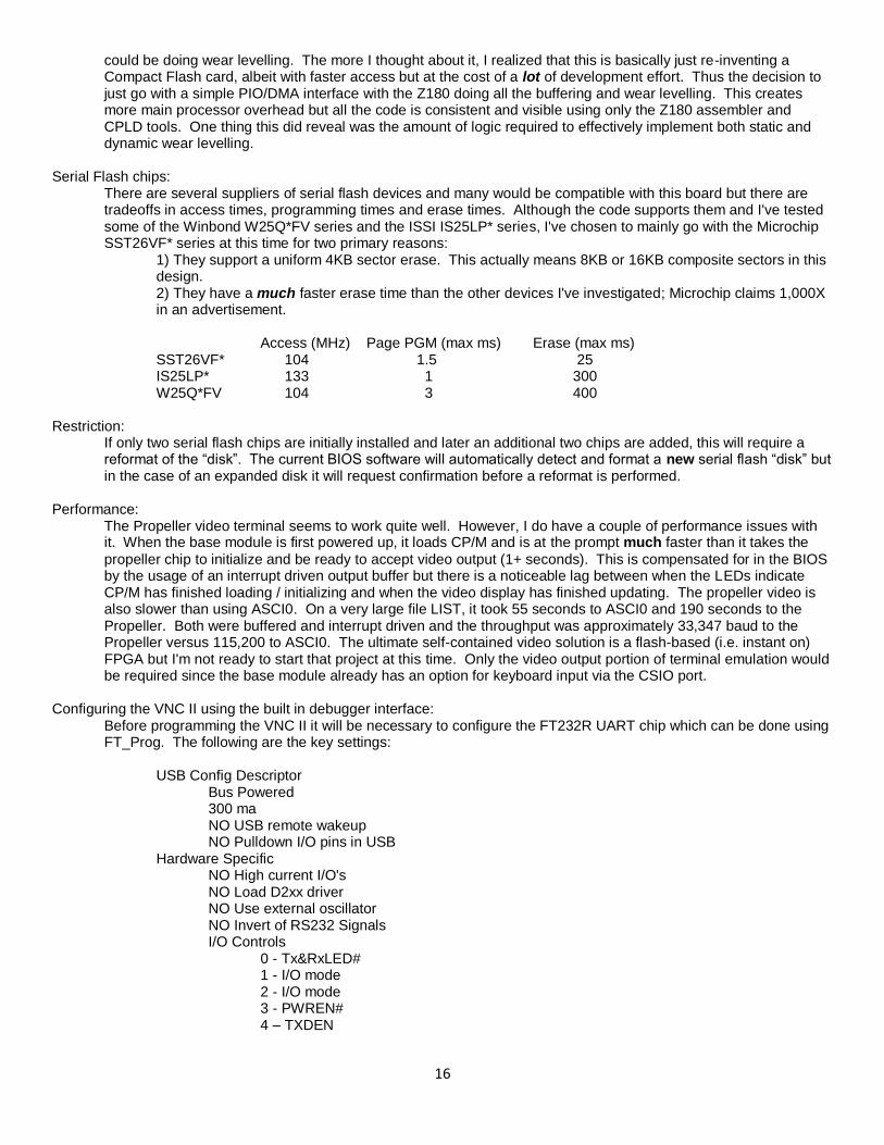
Serial Flash chips:
There are several suppliers of serial flash devices and many would be compatible with this board but there are tradeoffs in access times, programming times and erase times. Although the code supports them and I've tested some of the Winbond W25Q*FV series and the ISSI IS25LP* series, I've chosen to mainly go with the Microchip SST26VF* series at this time for two primary reasons:
1) They support a uniform 4KB sector erase. This actually means 8KB or 16KB composite sectors in this design. 2) They have a much faster erase time than the other devices I've investigated; Microchip claims 1,000X in an advertisement.
Access (MHz) Page PGM (max ms) Erase (max ms) SST26VF* 104 1.5 25 IS25LP* 133 1 300 W25Q*FV 104 3 400
Restriction:
If only two serial flash chips are initially installed and later an additional two chips are added, this will require a reformat of the “disk”. The current BIOS software will automatically detect and format a new serial flash “disk” but in the case of an expanded disk it will request confirmation before a reformat is performed.
Performance:
The Propeller video terminal seems to work quite well. However, I do have a couple of performance issues with it. When the base module is first powered up, it loads CP/M and is at the prompt much faster than it takes the
propeller chip to initialize and be ready to accept video output (1+ seconds). This is compensated for in the BIOS by the usage of an interrupt driven output buffer but there is a noticeable lag between when the LEDs indicate CP/M has finished loading / initializing and when the video display has finished updating. The propeller video is also slower than using ASCI0. On a very large file LIST, it took 55 seconds to ASCI0 and 190 seconds to the Propeller. Both were buffered and interrupt driven and the throughput was approximately 33,347 baud to the Propeller versus 115,200 to ASCI0. The ultimate self-contained video solution is a flash-based (i.e. instant on) FPGA but I'm not ready to start that project at this time. Only the video output portion of terminal emulation would be required since the base module already has an option for keyboard input via the CSIO port.
Configuring the VNC II using the built in debugger interface:
Before programming the VNC II it will be necessary to configure the FT232R UART chip which can be done using FT_Prog. The following are the key settings:
USB Config Descriptor Bus Powered 300 ma NO USB remote wakeup NO Pulldown I/O pins in USB Hardware Specific NO High current I/O's NO Load D2xx driver NO Use external oscillator NO Invert of RS232 Signals I/O Controls 0 - Tx&RxLED# 1 - I/O mode 2 - I/O mode 3 - PWREN# 4 – TXDEN
17
After configuring the FT232R, the user can then use either FT_Prog or V2Prog to program the VNC II. The current ROM being used is "V2DAP-V2.0.0-SP1.rom".
Configuring the FT232H EEPROM using FTPROG:
Before using an IOX board with an FT232H chip, it will be necessary to configure it’s EEPROM using FT_Prog. The following are the key settings:
USB Config Descriptor Self Powered Max bus power: 0 ma USB String Descriptors Product Description: Z180 – FT232H Hardware Specific Suspend on ACBUS7 low Port A Hardware 245 FIFO Driver Virtual COM port I/O Controls C9 - Tx&RxLED#
W5100 Misunderstanding and Possible Errata:
As part of my design verification I tried to do a memory test of the W5100's buffer. I can understand why my test fails to write into the Rx buffer but I have also noticed an odd behaviour when trying to read the Tx buffer. A 1KB test pattern was first written to the TX buffer then it was read back and compared to the original. Most of the data is correct but there are occasional discrepancies where the data from address+1 (odd byte) is returned from a read of address+0. This appears to be dependent on timing and/or the total amount of data read. A single byte read with a relatively long delay after previous reads always returned the correct value. I have thoroughly investigated my interface and cannot spot a potential problem. Likewise, a test of another 8-bit interface (MPZ4) using the same interface technique has not shown any kind of similar behaviour. Further research found a forum response from WIZnet stating that the Tx buffer cannot be read. At this time, I am accepting that this is correct and it is not possible to perform a legitimate host-based memory check of the W5100 buffer area. Note that my memory testing was done after verifying the basic W5100 functionality test and that it could connect to a router and handle PINGs.
Functional differences in revision levels: V1.0 - First PCB for validation purposes - Requires several modifications in order to use some of the features
V1.1 - Multiple required changes - Serial flash now has a dedicated LED indicating activity - Supports interrupts on the W5100 SPEED line; i.e. LINK at 100Mbps but without the RX/TX transitions V1.2 - Change SC70 packages to SOT23
18
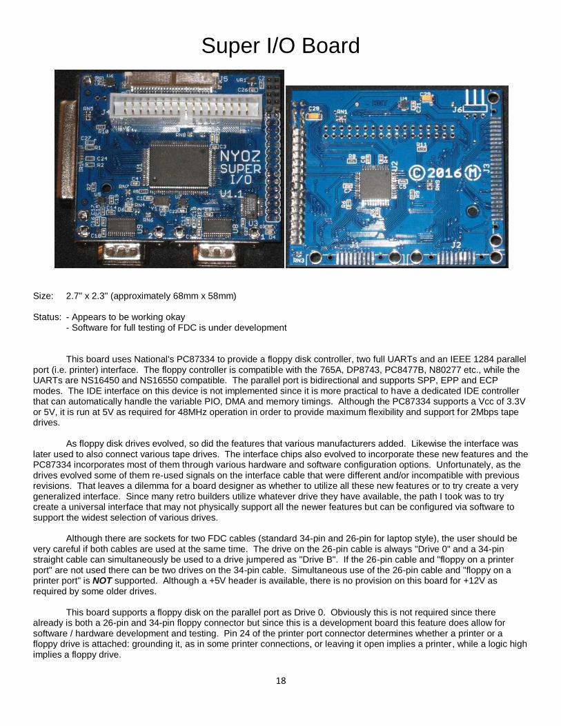
Super I/O Board
Size: 2.7" x 2.3" (approximately 68mm x 58mm) Status: - Appears to be working okay - Software for full testing of FDC is under development This board uses National's PC87334 to provide a floppy disk controller, two full UARTs and an IEEE 1284 parallel port (i.e. printer) interface. The floppy controller is compatible with the 765A, DP8743, PC8477B, N80277 etc., while the UARTs are NS16450 and NS16550 compatible. The parallel port is bidirectional and supports SPP, EPP and ECP modes. The IDE interface on this device is not implemented since it is more practical to have a dedicated IDE controller that can automatically handle the variable PIO, DMA and memory timings. Although the PC87334 supports a Vcc of 3.3V or 5V, it is run at 5V as required for 48MHz operation in order to provide maximum flexibility and support for 2Mbps tape drives. As floppy disk drives evolved, so did the features that various manufacturers added. Likewise the interface was later used to also connect various tape drives. The interface chips also evolved to incorporate these new features and the PC87334 incorporates most of them through various hardware and software configuration options. Unfortunately, as the drives evolved some of them re-used signals on the interface cable that were different and/or incompatible with previous revisions. That leaves a dilemma for a board designer as whether to utilize all these new features or to try create a very generalized interface. Since many retro builders utilize whatever drive they have available, the path I took was to try create a universal interface that may not physically support all the newer features but can be configured via software to support the widest selection of various drives. Although there are sockets for two FDC cables (standard 34-pin and 26-pin for laptop style), the user should be very careful if both cables are used at the same time. The drive on the 26-pin cable is always "Drive 0" and a 34-pin straight cable can simultaneously be used to a drive jumpered as "Drive B". If the 26-pin cable and "floppy on a printer port" are not used there can be two drives on the 34-pin cable. Simultaneous use of the 26-pin cable and "floppy on a printer port" is NOT supported. Although a +5V header is available, there is no provision on this board for +12V as required by some older drives. This board supports a floppy disk on the parallel port as Drive 0. Obviously this is not required since there already is both a 26-pin and 34-pin floppy connector but since this is a development board this feature does allow for software / hardware development and testing. Pin 24 of the printer port connector determines whether a printer or a floppy drive is attached: grounding it, as in some printer connections, or leaving it open implies a printer, while a logic high implies a floppy drive.
19
The PC87334 device supports an IrDA (Infrared Data Association) option for UART 2. This has been implemented by using DTR2 as a select signal for the RS-232 versus IrDA interface since it is always inactive when the UART is in IrDA mode. When DTR2 is active, the RS-232 interface is selected. Note that this also requires a bit in the IRC register of the PC87334 to be configured to select between the two modes. Although the board has been designed to support the IrDA interface, the actual IrDA hardware has not been tested at this time. In order to fully support this feature it would require considerable software development to create a reliable protocol. The I/O addressing on this board is performed by the PC87334 using six bits from the address bus, three fixed inputs and two logic-generated addresses. This mechanism is a bit convoluted but ends up making the actual interface quite simple with minimal external logic which only needs to generate the IORD*, IOWR* and two address signals. The PC87334's addresses are complicated by the fact that the parallel port's ECP mode actually has two I/O ranges: base and base+400h. This has been accommodated and while it could also have been accomplished more easily by using 16-bit I/O addresses, that would have forced all other I/O in the entire system to use IN0 and OUT0 type instructions. The final result of this re-mapping is the chip now has thirty-two contiguous 8-bit I/O addresses at 60-7Fh plus eight contiguous FDC address at B8-BFh. Since external logic was required to create the four vectored interrupts, a small CPLD was used to minimize the parts count. The layout of this board is certainly not the "prettiest". I chose to mount the D-sub connectors below the board in order to minimize the leverage effect that would have come from mounting connectors and cables above the board. However, I also chose to mount the PC87334 chip on the top of the board to facilitate easy probing and debugging. Unfortunately this combination required extra vias to correctly orient the various pins to connections. I also had the board about 3/4 routed when I discovered and corrected a physical dimension error that was introduced when I changed the D-sub connectors from top mounted to bottom mounted. Note that the surface mount connectors are not as rigid or robust as the more normal through-hole D-subs. This is fine for testing the boards but if the user anticipates any rough handling then a metal interconnecting frame should be added to the three connectors in order to add rigidity and limit flexing. There is a real allure to using PC-oriented chips in non-Intel system since there is a wide selection, they are readily available at a reasonable cost and some are highly integrated. However, there are also some potential "gotchas" that the designer has to be aware of. With the use of the PC87334 in a 33 MHz Z180 system there are three noteworthy issues (besides the addressing) that I identified:
- The PC87334 has a very slow turn off time (13 - 25ns) for the data tri-states during reads. This is compounded by the need for 18ns of stable address before the RD* or WR* signals. If the RD* / WR* decoding takes 5ns then this timing can just be theoretically met but is definitely pushing a boundary (0.5ns) which is probably violated
when rise/fall times are taken into account. The solution was to add a fast external tri-state buffer for isolation. - Intel multi-channel DMA controllers produce a single terminal count (TC) signal whereas the Z180 has unique TEND0 and TEND1 signals for DMA0 and DMA1. This can easily be solved with a single NAND gate. Also note that there is a separate signal (i.e. decoded address) for DMA data versus PIO data. - Intel DMA controllers produce the TC signal to notify the peripheral that the current cycle is the last one whereas the Z180 sets the TENDx signal on the last write cycle. There is no conflict on transfers from memory to a peripheral device since the I/O write will be the last operation. However, on a Z180 DMA transfer from a peripheral to memory (i.e. I/O read) it will set the TENDx signal on the memory write and NOT on the I/O read (i.e. the last peripheral access). One could use the DMA interrupt on the Z180 instead of the peripheral interrupt when doing a read. This can also be kludged in software but it can be messy and may resort to polling the device. Alternatively, extra external logic can be used to generate the proper TC signal and if I design a board with a larger CPLD, I'll use this method which would allow the software to simply be written according to the Intel-based datasheets.
Functional differences in revision levels: V1.0 - First PCB for validation purposes V1.1 - Corrected some addressing and initialization signals - Added LEDs for serial port's CTS & RTS signals - Added some required pull-up resistors V1.2 – Separate resistors for LEDs on UART2
### FDC Connector pinouts

20
UARTs - DE-9M : 1 - DCD - Input 2 - Rx - Input 3 - Tx - Output 4 - DTR - Output 5 - Ground 6 - DSR - Input 7 - RTS - Output 8 - CTS - Input 9 - RI - Input Parallel - DB-25F: WRITE* 1 STB* INDEX* 2 D0 TRK0* 3 D1 WP* 4 D2 RDATA* 5 D3 DSKCHG* 6 D4 MSEN0* 7 D5 DRATE0 8 D6 MSEN1 9 D7 DR1* 10 ACK* MTR1* 11 BUSY / WAIT* WDATA* 12 PE WGATE* 13 SLCT DENSEL* 14 AFD* / DSTRB* HDSEL* 15 ERR* DIR* 16 INIT* STEP* 17 SLIN* / ASTRB* Ground 18:23 Ground +5V 24 PNF* (Note 1) 25 Ground Note 1: Open or grounded implies a printer whereas a logic high implies a floppy drive

21
MEM-X - Memory Expansion Board
Size: 3.1" x 2" (80mm x 50mm) Status: - Functionally tested and working - Enhanced "disk" software under development Features: - Maximum of 32MB flash memory or 16MB of SRAM or various permutations The purpose of this board is to optionally allow for a larger flash device that might be found on the full system as the main flash device or to just provide for a lot of extra flash and/or RAM memory configured as "disks". The main flash device on the proposed full system is accessible as both the boot ROM and as a flash disk, similar to the base module described herein but it is considerably larger in size (8MB) than the base module's 512KB. The memory on this expansion board is 16-bit wide with a 128KB window and is accessible either via 8-bit memory mapping or via a 16-bit custom DMA controller (except for flash writes). Flash writes are always via two 8-bit writes, first to an even address with zero wait states and then to address+1 with two wait states. The use of x16 flash devices versus x8 devices reduces the programming times (i.e. delays) by one half. There is space on this board for four flash and/or RAM chips; the flash chips can each be 2MB, 4MB or 8MB while the RAM chips can be 2MB or 4MB each. The RAM and flash on this board are each treated as logically continuous arrays which can then be partitioned into "disks". If 2MB to 6MB of RAM is installed, the current firmware uses it as an expansion of the RAMdisk in the base module's RAM such that the directory is in zero-wait main RAM while the expanded data area on this board is accessed with one wait state. If 8MB or more of RAM is installed then it creates a second (and possibly third) unique RAMdisk under CP/M 2. Likewise, the first logical flash drive is allocated as a maximum of 8MB due to the CP/M 2.2 loader and any additional flash space is configured as appropriate. Note that the CONFIG utility can assign drive letters and/or disable various memory disks. It can also force the allocation of disks greater than 8MB but they will not be accessible under CP/M 2. To truly emulate the future full system, an 8MB flash device should be installed and a switch on this memory board can then be set which will disable the base module's flash device as the boot ROM. When this switch is active, the default "ROM" disk (i.e. drive letter) points to the drive on the MEM-X board and the base module's "ROM" disk is not accessible. Simply turning the switch off or removing the memory expansion board makes the base module revert to its on-board flash device as the boot ROM and as the default "ROM" disk. Thus the "ROM" disk drive letter always points to the device that the system was booted from. There is also an MRAM device on this board which is used for flash device wear levelling and contains the mapping tables and control information. If there are no flash devices on this board (i.e. only RAM) then the MRAM device does not need to be installed. The wear levelling algorithm extends across all flash devices installed on this board with
the exception of the first 64KB of U1 which is reserved as a boot area and should see very little change after initial development. If additional flash devices are added, they will be recognized at the next system reset and will then partake in the overall wear levelling.

22
RESTRICTION: This board does not need to be fully populated with memory chips. However, only the first device (U1)
has an option to allow for physically write-protecting the boot block of a flash device and also of being the system boot device. In order to utilize this feature, only bottom-boot flash devices should be installed in U1. Once a board with flash devices has gone through the first reset / initialization, additional flash chips can be added to expand the size and/or number of flash drives, but they MUST be added in ascending device positions in order to retain the integrity of the existing drive(s). If only RAM is initially being installed then it is recommended to start populating it from the highest device number (U4) to the lowest which means U1 (the bootable device) is the last one to be populated. Note that the sequence of U1=flash, U2=RAM, U3=flash and U4=RAM will also be handled correctly by the software but only if the flash at U1 is installed before or at the same time as U3.
N.B. The physically write protectable boot block is 16KB for 2MB & 4MB flash chips at U1 while it is the full 64KB of reserved area for 8MB flash chips. It is recommended that if a flash chip is installed at U1 then it should be an 8MB bottom-boot device (i.e. SST39VF6401B) for maximum protection in a manner consistent with the full system. Also note that each memory device has a corresponding jumper wire that must be installed when adding a memory device since it configures the physical layout for RAM versus Flash. At this time, there is still a requirement for the initialization software to also detect and set whether each installed device is flash or RAM rather than automatic hardware detection. Design notes:
There is provision for MRAM on the base module which could have been used but this is a development system and it would require a lot of software to guarantee and maintain flash integrity if various MEM-X boards were interchanged. The 128KB of MRAM on this board is larger than actually required, especially if only one or two flash chips are installed. Originally this board was designed for eight memory devices but it was decided to trim it back to just four devices. The next smaller available MRAM device (32KB) is about 1/2 the cost but 1/4 the capacity and would only hold the tables for two 8MB flash devices. Thus there would either need to be a restriction of 16MB total flash or the option of a second MRAM device if more than 16MB of flash chips were installed. Unfortunately the pinout for the smaller MRAM device is significantly different and thus the larger MRAM chip was left in place for maximum flexibility.
The extra MRAM space has been put to good use. One of the performance issues when using flash memory as a "disk" is that every directory write (128 byte logical sector for CP/M & MP/M) requires a full physical sector write (4KB) to guarantee integrity and every written word requires a programming delay. There is also an erase operation required for the old physical sector. By using MRAM to hold the directory there is the potential to save up to ~45 ms on every directory update which is about 1 full second for every 11 basic file creations. This is a noticeable delay when copying groups of files to a flash drive (i.e. PIP flash:=*.*).
It would be relatively easy to enhance this board such that multiple MEM-X boards are allowed within a system but there are no plans to do so. If an application really requires more flash and/or RAM than provided on this board then I believe it would be time to consider using either an SD card or a CF card which are available in various capacities. This board was primarily meant to be relatively simple for development purposes (SW & HW) but with a fast interface. It has a significant amount of space when compared to 1970's systems but it was not meant as a large bulk storage alternative.
It would have been possible to design this board to use fast SRAM devices and thus avoid the one wait state penalty during RAM accesses. The design trade off was that fast SRAMs are considerably more expensive than the slower devices used (more than twice as much) and also consume a lot more power which also generates more heat. Since the SRAM(s) on this board are used as "disks", it was felt that the extra cost and power could not be justified. Likewise, faster flash devices with one wait state (versus two) could have been used but at the time of development they were not available in the same densities and with the same other specifications (4KB sector and fast erase / program times). The largest similar device that requires only one wait state was only 1/8 the maximum size of the actual devices used and thus would have required many more devices for a similar total capacity. An increase in the number of devices would also have required a larger CPLD. Again, since these flash devices are primarily used as "disks" it was felt that the one extra wait state (two total) was a worthwhile trade off. Note that these "disks" are treated as non-removable to CP/M & MP/M and thus avoid a lot of the directory reads that a removable device incurs.
Update: There are now larger and reasonably-priced fast 4MB SRAMs from ISSI. Unfortunately their TSOP I packages are not pin-compatible with the more commonly available slower devices that this board was designed around. Flash performance considerations:
There is a small overhead on every logical sector read or write before the memory-to-memory DMA transfer in order to determine if the actual data area is in MRAM, in a base module RAM banked buffer or on the actual flash
23
device. Read data that is not in MRAM or a buffer is directly transferred from the flash device without buffering. Flash writes for data that is not in MRAM are always buffered and may result in the pre-read of a full physical sector if the write is not to an unallocated block. Writing the physical sector back to flash incurs the highest overhead and thus is deferred until a directory write, a warm boot or a requirement to reuse the buffer for other data. A power-off with dirty buffer may result in some loss of data but the directory should be intact, albeit possibly with some unused blocks marked as allocated. A simple CTL-C will ensure all dirty buffers have been written and a future enhancement will add a timer to also flush dirty buffers after a prolonged idle time.
Functional differences in revision levels: V1.0 - First PCB for validation purposes - Not compatible with the MPZ4 multiprocessor board without the V1.1 upgrade
V1.1 - Added an address line to the I/O decoder to limit the I/O chip select to 8 addresses versus 16 - V1.0 boards can be upgraded with one trace cut and two jumper wires V1.2 - Added a LED to indicate activity - Changed how the ‘245 transceivers are enabled

24
ATA - CF, 2.5" ATA and SATA Board
Size: 2.9" x 2.5" (approximately 72.5mm x 63 mm) Status: - CF & ATA working - SATA still being tested Features: - CPLD based 3.3V wing - A single 44 pin connector to interface to 2.5" ATA hard disks
- Both master and slave can exist on the same cable - Try to keep the cable relatively short
- Dual CF (Compact Flash) cards - The specification that I used for this interface (Rev. 4.1) clearly states that only one CF device
should be attached to the CF bus when operating in the advanced timing modes (PIO > 4, DMA > 2, UDMA > 2).
- I am aware that some developers have had issues when using master / slave CF cards. The reason I included both connectors is to investigate these issues. However, due to the above restriction only the master card should be used if the CPLD is upgraded to test the advanced timing modes.
- Although there is hardware detection and an interrupt when a card is inserted or removed, at this time the software routines do not support card changes. A RESET must be performed to recognize a new card
- A SATA port with support for a master device only - Supported data rates are PIO 0-4 and DMA 0-2 with no support for UDMA. I am aware of various techniques to read CF cards in 8-bit mode and various ATA interfaces similar to GIDE as developed by Tilmann Reh. In fact, many years ago I independently designed and successfully implemented an interface similar to GIDE. I chose to not use this type of interface in this project for two main reasons:
1) According to the ATA specifications, IDE devices initialize in PIO Mode 0 and can then be programmed to operate at a higher data rate. The IDE register read/write timing specification in Mode 0 calls for a 290ns pulse and 30ns of write data hold time. This is much longer than the Z180 signals in this system, even with the Z180's maximum wait states, and would require the implementation of external hardware wait states. While wait states can't be eliminated for PIO reads, they can be optimized with CPLD logic for various I/O operations. Writes can also be optimized to not require any CPU wait states unless there are multiple back-to-back writes.
25
2) From the outset, the NYOZ system was designed with a 16-bit memory bus and the objective of reducing bus
accesses via the use of 16-bit DMA operations. This necessitated a unique ATA to Z180 interface design in order to take advantage of it.
This board primarily allows for the software development of IDE interfaces during the FPGA board design and testing cycle. While I'm not the happiest with this board, the reason I chose to develop it is that I already had a CPLD designed and tested for a different system which implemented the interface to two ATA channels (each with a master and slave) and had its own 16-bit DMA controller. The downside of this CPLD is that the PIO interface uses the WAIT* signal on most reads and the DMA interface (multiword only without ultra) holds onto the system bus for as long as the ATA device is requesting data transfers. Another performance issue is that there is only one combined PIO and DMA controller so even though there were two logical channels and four possible devices, their data transfers cannot overlap. The advantage for me is that it has been proven to work in a different system and there was minimal CPLD and software development required. The layout of this board certainly isn't optimal but it was designed to co-exist with the XIO board and to clear the various connectors. I really didn't want to spend a lot of time doing the design and it is basically a quickly designed board to allow software development before spending the time to learn, design and experiment with the FPGA-based ATA board. Another downside of the "quick" layout is that I had to use a larger CPLD (i.e. macrocells) since the board was primarily designed for easy layout and there was minimal optimization of the pins to CPLD function blocks. Optimization of the CPLD and pin layout would have allowed for the use of a smaller (i.e. macrocells) and cheaper CPLD. The next smaller CPLD is pin compatible and can still be used if just two of the three interfaces are populated. When adding a ribbon cable for a 2.5” IDE drive, the orientation of Pin 1 should be carefully noted. The orientation was originally designed to allow for a very short cable to a physical drive for testing purposes. In the case of a DOM (Disk On Module) it will likely require the DOM to be added upside down. Enhancements:
The original CPLD only supported two channels whereas all the signals have been included for three channels which have now been implemented; CF, 2.5" IDE and SATA. Another possible enhancement is the current CPLD only uses the slowest PIO and DMA data rates when there is a master and slave on the same channel whereas each device should have independent (possibly the same) data rates. Likewise, a future investigation is to look at adding higher PIO and DMA rates as supported by some CF cards. Note that this board does not have the series resistors required for UDMA. Multiple independent DMA controllers within the CPLD would be a nice enhancement but it really isn't practical without a lot of board rework due to the shared signals on the channels and the pin count of the current CPLD package.
Reference:
PIO mode 6 would allow for one less CPU wait state. However, this is really only applicable for CF ATA register I/O since the software only uses PIO data transfer for the one-time READ IDENTIFY which is used during initialization. After a device has been identified, data I/O always uses DMA. At this time, the PIO mode 5 & 6 enhancement is a very low priority.
Restriction:
At this time, the DMA channel only supports transfers to/from an even address. This has been taken into consideration in the [de]blocking buffers but should also be taken into consideration if the user is making modifications to the software. Implementing an odd address DMA controller is feasible but would require both development effort and would incur either a significant performance penalty or extra logic and buffering in the CPLD.
N.B. If this board is stacked on top of another board such as the IOX Board, there needs to be a pair of jumper wires between the two boards to properly chain the BUSACK* and INT_EN* signals. There is also a 2mm jumper plug that needs to be installed. A chain-out header is also included in case other boards are stacked above this board. This is not the cleanest methodology but it gets around the difficulty of creating a chained stackable header without resorting to split and/or mixed-mode headers. Most of the development effort has been centered on testing one wing at a time. Comment:
I originally planned this board to use ESATAp to simplify cabling but once again this board has proved the pitfalls of low-volume prototyping. I normally try to be careful in my selection of components to select items that are available from multiple distributors. Such was the case for both the ESATAp and reverse CF connectors.

26
However, there was a significant elapsed time between when I selected components and checked their availability to when I had finished the board design and was ready to order the required parts to actually fabricate it. In the elapsed interval, the ESATAp connector became end-of-life not available and the reverse CF connector I selected became non-stocked with minimum order quantities in the 1,000's. The CF connector substitution was relatively straightforward but required a bit of time to create a new CAD library part. The solution for the ESATAp connector was a bit more of a kludge: it was changed to a simple SATA connector plus a separate header was added for +5V power. The cabling isn't as clean as the original design but is still totally functional for test purposes.
Functional differences in revision levels: V1.0 - First PCB for validation purposes
V1.1 - Added POR* from CPLD to JM20330 - Added ground connection to CSEL - Added RESET* to JTAG header
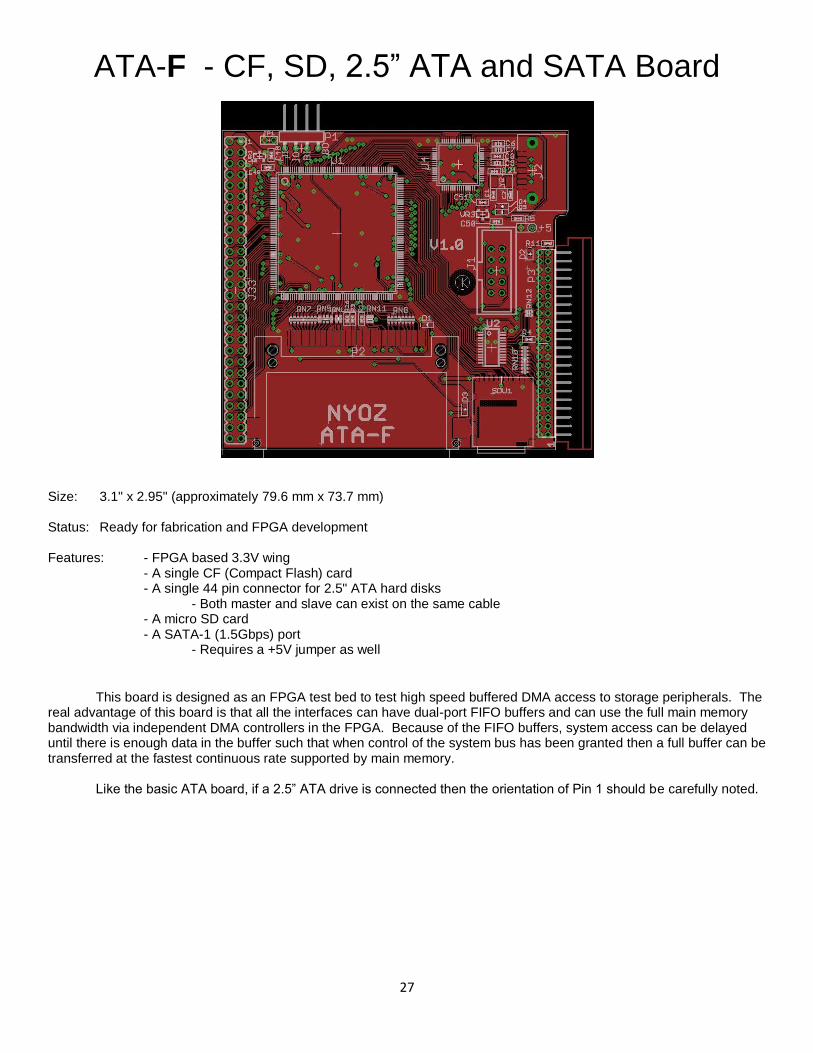
27
ATA-F - CF, SD, 2.5” ATA and SATA Board
Size: 3.1" x 2.95" (approximately 79.6 mm x 73.7 mm) Status: Ready for fabrication and FPGA development Features: - FPGA based 3.3V wing
- A single CF (Compact Flash) card - A single 44 pin connector for 2.5" ATA hard disks
- Both master and slave can exist on the same cable - A micro SD card - A SATA-1 (1.5Gbps) port - Requires a +5V jumper as well
This board is designed as an FPGA test bed to test high speed buffered DMA access to storage peripherals. The real advantage of this board is that all the interfaces can have dual-port FIFO buffers and can use the full main memory bandwidth via independent DMA controllers in the FPGA. Because of the FIFO buffers, system access can be delayed until there is enough data in the buffer such that when control of the system bus has been granted then a full buffer can be transferred at the fastest continuous rate supported by main memory. Like the basic ATA board, if a 2.5” ATA drive is connected then the orientation of Pin 1 should be carefully noted.
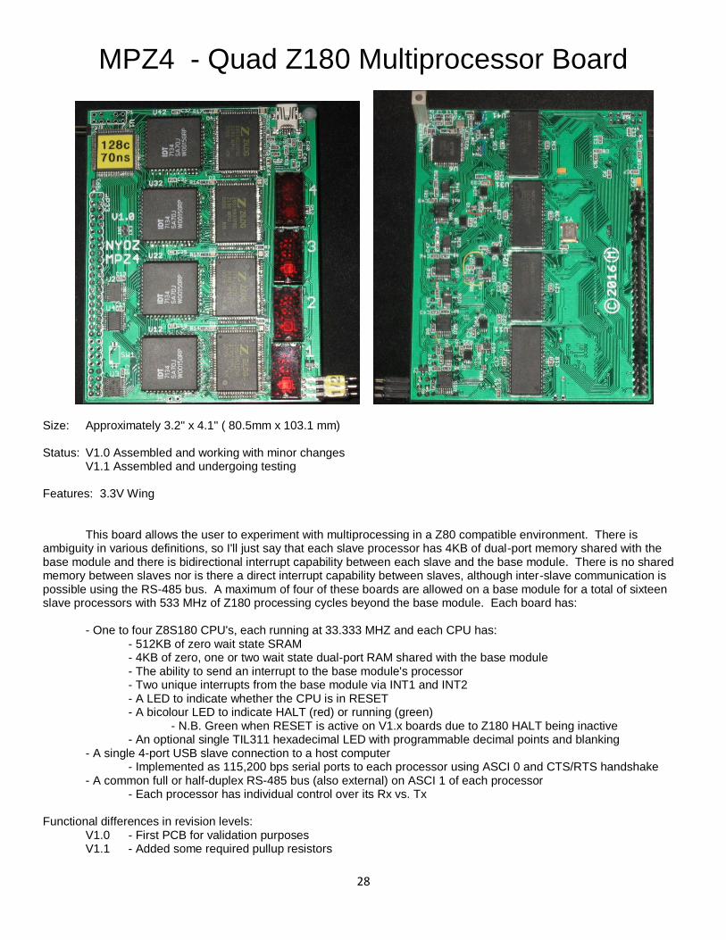
28
MPZ4 - Quad Z180 Multiprocessor Board
Size: Approximately 3.2" x 4.1" ( 80.5mm x 103.1 mm) Status: V1.0 Assembled and working with minor changes V1.1 Assembled and undergoing testing Features: 3.3V Wing This board allows the user to experiment with multiprocessing in a Z80 compatible environment. There is ambiguity in various definitions, so I'll just say that each slave processor has 4KB of dual-port memory shared with the base module and there is bidirectional interrupt capability between each slave and the base module. There is no shared memory between slaves nor is there a direct interrupt capability between slaves, although inter-slave communication is possible using the RS-485 bus. A maximum of four of these boards are allowed on a base module for a total of sixteen slave processors with 533 MHz of Z180 processing cycles beyond the base module. Each board has: - One to four Z8S180 CPU's, each running at 33.333 MHZ and each CPU has: - 512KB of zero wait state SRAM - 4KB of zero, one or two wait state dual-port RAM shared with the base module - The ability to send an interrupt to the base module's processor - Two unique interrupts from the base module via INT1 and INT2 - A LED to indicate whether the CPU is in RESET - A bicolour LED to indicate HALT (red) or running (green) - N.B. Green when RESET is active on V1.x boards due to Z180 HALT being inactive - An optional single TIL311 hexadecimal LED with programmable decimal points and blanking - A single 4-port USB slave connection to a host computer - Implemented as 115,200 bps serial ports to each processor using ASCI 0 and CTS/RTS handshake - A common full or half-duplex RS-485 bus (also external) on ASCI 1 of each processor - Each processor has individual control over its Rx vs. Tx Functional differences in revision levels: V1.0 - First PCB for validation purposes V1.1 - Added some required pullup resistors

29
This environment could be used to create a tightly-coupled MP/M : CP/NET configuration where all the common "disk" I/O is performed by the base module running MP/M and each slave is essentially a CPU/RAM module running CP/M with an independent serial port (i.e. console) and a local RAMdisk. Although I haven't done enough research yet, this environment might be a prime candidate for Software 2000's TurboDOS. Alternatively, it could be treated as a set of extra CPU cores to process a compute-bound algorithm such as a Mandelbrot set. Another concept might be that of independent processors whose only interactions with the base module is during the loading process and afterwards they operate as independent systems with all I/O over their two serial ports. For those that prefer more modern jargon, the slaves are essentially software containers with dedicated processors. Obviously there was a choice of whether to use a basic Z80 or a Z180 for this board and the latter was chosen for several reasons. The primary reason was for performance since the Z8S180 is available in a 33 MHz version versus only 20MHz for a Z80. The two UARTs on the Z180 are put to good use and DMA0 is used to increase memory-to-memory copy performance. The Z180 MMU allows for a much larger addressable memory space that can be used for buffering, a local RAMdisk or other memory-based functions. The only consideration for using a Z80 versus a Z180 on this type of board would be if the user wanted CPU-only boards with no peripherals, minimal memory and minimal board area. Otherwise the Z180 makes a lot more sense to me and should only cost a few dollars more, including the much larger SRAM. The processors on this board do not have a unique ROM. Instead, during power-on they enter the reset state and the host can then load an initialization routine into the dual-ported memory followed by releasing the reset state. At that point the slave and the host can then communicate via interrupts or polling and exchange data in the shared memory. This communication can either be to continue loading more program data or to enter a "running" mode where the slave and host interact as required by the software. Note that the dual-ported memory is in the lower 512KB of the slave's 1MB address space while the regular RAM is in the upper 512KB of the address space. This is easily handled by the Z180's MMU. The base module addresses a unique dual-port RAM as follows: EXT_MEM* + A18 + A17 = MPZ4 memory range (A18=A17=1) A16, A15 = MPZ4 board select (0-3) A14, A13 = MPZ4 Slave select (0-3) A12-A0 = 8KB address range for each dual-port memory (only 4KB currently implemented) The base module's bank number for each dual-port memory device can be calculated as: 60h + board*8 + slave*2 In order to communicate with the base module (i.e. the common "host" or "master") these slave processors can set flags and data in the dual-ported RAM to indicate the request type and then generate an interrupt for the base module. After processing the request, the base module can then also set flags and data in the dual-ported RAM and generate an interrupt back to the slave. Of course, polling for a change is also viable. Note that the current implementation does not have "wait" capabilities on the dual-ported RAM to detect and control simultaneous access to a single memory byte. By using separate data areas for each set of flags, the dual write contention is avoided. In order to detect the actual individual flag change, each side should retain a copy of the previous flags and set/detect an inversion of a flag to indicate the actual request. The host --> slave interface actually has two unique interrupts and one of them could be used for a non-acknowledged function such as a watchdog signal or a real-time clock signal. The basic design includes a four port USB controller connected to ASCI 0 of each slave which can be used as a console or other serial communication link. However, it would also be possible to include interrupt-based communication with the base module via the dual-port memory whereby console data is sent to/from the base module for inclusion on a common console attached to the base module, such as the Propeller chip on the IOX board. In that case, the USB circuitry would not need to be populated unless it is required for other purposes. Due to the minimum configuration, each slave has only one latched output-only port for both the hex LED control functions and the RS-485 TXEN signal. It is up to the slave to retain a memory-based copy of the previous data and any updates should only change the appropriate bits (LED or TXEN). I did consider adding more I/O capabilities to each slave in order to allow them to possibly operate as I/O processors but that would take more hardware and board space. Moreover, the base module and other wings already have lots of efficient I/O capabilities. If new and unique system I/O capabilities are required, they will most likely be designed into a new and dedicated wing for the base module.
Some of the above restrictions could have easily been removed with the use of additional logic and/or a larger CPLD on this board. For example, finer I/O port resolution and non-conflicting common semaphores. However, one of

30
the objectives of this board was to create a minimal design in minimum space. Besides the physical CPLD size (i.e. pins), every additional signal used by a slave is actually repeated times four. That doesn't sound too bad until one tries to route the board and requires extra space, vias and other issues. For now, I'm sticking with the KISS approach which is fully functional. This board generates Mode 2 vectored interrupts to the base module and it supports INT_ENABLE* daisy chains, both as input and as output. If the INT_ENABLE* comes from a daisy chain input then a 2mm jumper must be placed on the header labelled EXT INT. It does not have an onboard DMA controller so it does not require daisy chaining of the BUSACK* signal. This board can be built with less than four slave processors and several of the related support ICs can then also be left out. However, the USB controller documentation is somewhat ambiguous as to whether it has internal pull-ups on the two inputs coming from each slave's ASCI 0 port. Short jumper wires should be installed along the indicated PCB lines in this case. In the event the slave processor is later populated, the jumpers can easily be removed. The V1.x versions of this board do not use the CSI/O interface of the Z180. If a four-layer version of this board is created, a possible enhancement will be to implement this interface. Three configurations have been considered: - Slave 1 <-> Slave 2 and Slave 3 <-> Slave 4 - Slave 1 <-> Slave 2 and Slaves 3 & 4 as listeners only
- A common bus using Slave 1 as a master. The issue with a common bus is there must be extra software logic for controlling the bus and tri-state logic needs to be added to the TXS pins. To prevent short circuits from feeding back into the Z180s during simultaneous transmits, this would probably require an interface driver since open-collector (drain) logic would limit the data rate.
RS-485:
The external plug is used to configure this interface for half or full duplex in addition to possibly interfacing the board to other RS-485 devices including other MPZ4 boards and the base module. This plug should also contain any required termination resistors since the number of them and their value is dependent upon the mode and network layout. In half-duplex mode, any device on the network could be designated as the master controller and this is strictly a software function. The V1.x version of this board support full duplex mode but it does not support any of the four slave processors being used as the master controller. However, with proper wiring, the base module's ASCI 1 can act as either a master controller or a slave controller in a full-duplex RS-485 network. In an RS-485 network using only Z180 interfaced boards, the Multi Processor Mode of ASCI 1 can be used to minimize interrupts and data processing in non-master devices, albeit at the sacrifice of not being able to use the parity bit.
Design notes: Although this board primarily uses 5V for cost and complexity reduction, it is on a 3.3V wing rather than a 5V wing in order to gain access to additional base module address lines plus the external memory select signal. The output signals from this board to the base module are all 3.3V. Overall, this board consumes a lot of power and once it is operational this will be measured. It is possible that an additional +5V / GND source may need to be added to handle the extra current, especially if a stack of four of these boards is to be used. Note that TIL311 hex displays can take up to 190ma each or 760ma for four of them on a board ... four boards could require over 3 Amps just for these displays!
Unless one is using the rare INL0397-1, it is recommended that these displays be socketed and only installed when required for debugging purposes, especially when using multiple MPZ4 boards. This board was designed primarily for software experimenting rather than for future inclusion in a complete system. As such, development cost was an important consideration since the intent was not to turn it into a commercial product. One of the major impacts is that I chose to use new-old-stock memory chips that I had available in my spare parts rather than selecting newer and more modern devices. The implication is that although the test boards didn't cost me a lot to produce, they have 512KB of main RAM and these chips use more power than would be feasible with newer pin-compatible devices. The dual-port memory can consume a lot of power if both ports are operating at their maximum frequency. This power could be reduced by going to a smaller device (i.e. 1KB) and/or a 3.3V device. The 4KB 5V devices were selected for ease of interfacing and due to having a large supply of unused ones in my spare parts which resulted in no additional cost for them when populating and testing this board. It is envisioned that this memory will be primarily used for the booting of the slaves plus the interchange of data buffers so most of the time this memory will be in standby and at a significantly reduced power level. A configuration with four-port memory and only three slave processors was briefly

31
considered but given the price and availability it was quickly ruled out as a viable alternative. An FPGA was also considered for the shared RAM and although it would be much more flexible, that would take it beyond the KISS approach and involve a lot more development. The dual-port memory on this board uses the PLCC form factor rather than the LCC package as might be expected on a surface mount board. The reason was simply that this was the form factor of the chips that I had in my spare parts. Space was made available on the board for this larger package and one real advantage is that it makes layout / routing easier as there is room between pins to run a trace without having to switch layers and add vias. Likewise, the SOJ package for the RAM also makes routing easier than using a TSOP package. The majority of my dual-ported memory chips are actually 70ns which requires two wait states but I do have some 20ns chips that will run without wait states. Both speeds will be tested and the intelligent wait state generator on the base module can handle either type as required. Trivia:
The integrated circuits on the various boards in the NYOZ series use a variety of compact packages such as TQFP, TSOP, SSOP, SOT etc. After fabricating many of these boards, hand soldering the MPZ4 holds one surprise: the PLCC packages for the dual-port memory seems absolutely humungous! There is no real issues soldering them in place but it just seems weird working with such a thick package and a fully populated MPZ4 board is also noticeably heavier than the various other boards.
This board would definitely have been easier to lay out in four layers versus two layers and in fact could easily be changed to four layers with a slight reduction in overall size since two of the power tracks and extra ground width were added on edges. This board just slightly exceeded the 100mm dimension that many of the board houses use for a significant price step (double or triple the cost). At this time, there are no plans to try change it to four layers and less than 100mm but that should be relatively straightforward. The other dimensional issue was with the support post location used by some of the other wings. Due to heat dissipation, this board should be at the top of a stack of wings and possibly with only the relatively small MEM-X board above it. This board has its own unique support post location (i.e. hole) and this location clears other NYOZ boards and their connectors. If for some reason a wing with the common support is placed above this board, it can use a shorter support post that will rest on top of the second Z180. A big reason why this board was not originally layed out in four layers is that I use Eagle and have a fully paid Standard license which only supports two layers. The Maker version of the software which supports four layers (actually six) has a non-commercial clause that doesn't meet my requirements and I'm not ready to pay for the Premium version. It is my philosophy to always respect software licenses and this series of boards are examples of the boards that can be produced with the Freeware or Standard version of Eagle. It was also anticipated that this board would require at least one prototype fabrication / iteration to detect any basic design problems. One thought I had was that once the prototype board has been tested to then continue using Eagle to essentially convert the board to four layers but with some vias for the unrouted power / ground traces to the extra layers. The resulting board file could then be imported into an open source CAD program such as KiCad or a freeware program such as DesignSpark and the inner two power / ground layers could easily be completed. Update:
The entire licensing issues with Eagle have been radically changed from a purchase / upgrade model to a subscription model. Personally, I do not like the subscription model as it leaves the designer at the mercy of
future pricing changes and incompatible upgrades to the software whereas a purchase model usually allows a designer to update old designs so long as they still have the hardware and operating system to run the software. I will continue to use my purchased level of Eagle but may consider a very short-term subscription to Eagle in order to simplify a four layer upgrade.
There is a bit of discrete logic associated with each of the four slave processors. The alternative of a larger CPLD due to pin counts or an additional small CPLD would have introduced both a board area issue and a lot of routing issues. I also looked at using one of the low-power 16V8 PLD's for these functions but quickly reverted to discrete logic for two reasons: 1) Cost - although it takes a bit more assembly effort, discrete chips were cheaper. 2) Programming - The main CPLD on this board uses JTAG [re]programming whereas a PLD requires a unique programmer and they are not easily reprogrammed in-place when surface mounted. In order to reduce the parts count, the FT4232H circuit does not include an EEPROM which should not be a problem since it operates in basic UART mode. When the MPZ4 board is powered up and the USB cable is first connected to a Windows PC, Windows should search for and load the appropriate FTDI VCOM driver. The default configuration is 9600 baud and no flow control so the user will need to change that via Control Panel -> Device Manager -
32
> Ports -> USB Serial Port (??) -> Port Settings. The values should be updated to: 115200, 8, None, 1, Hardware Flow Control. Likewise, a terminal emulation program like HyperTerm will also need to be appropriately configured. Possible Enhancements:
The original design of this board uses the FT4232H IC for the quad serial to USB interface. The FTDI chips are well known, commonly available and I had all the utilities in place to work with them. Further research has indicated that the Silicon Labs CP2108 should also be a suitable bridge. The advantage is both a significant reduction in chip cost and a reduced parts count since it does not require either a crystal or external EEPROM and its on-chip regulator can accept a 5V input. One negative is that it appears a level translator would be required on 6 inputs from the Z180 ASCI ports. Another negative is that it uses a QFN footprint which is considerably harder to hand solder unless an extended footprint is used. Although I haven't revised the board to use this chip, it will definitely be given serious evaluation if significant rework is being performed on this board. One quirk with the LEDs on this board is that when a processor is in the reset state it's RESET LED is ON but the RUN/HALT LED is green which is the same as RUN mode. This is due to the HALT* signal being in the inactive state when the RESET* signal is active. An enhancement would be to turn the RUN/HALT LED completely off when in the reset state. Unfortunately this does not appear to be a simple change using just the currently available gates in this confined area of the board and will probably only be feasible if the board is changed to four layers.
ERRATA
In order to reduce the parts count on this board I used one oscillator, a single-gate flip-flop and two capacitors versus four crystals and 8 capacitors that would be required in the more normal configuration. The 33.333 MHz oscillator is divided by two and there are two Z180s running in 2X clock mode on each phase to try disperse switching activity on the board. This appears to work fine and has been verified both with an oscilloscope on the PHI outputs and with various software timing loops. The problem I've encountered is with the SLP instruction which appears to NOT stop executing instructions whereas the HALT instruction works as expected. In addition to also checking XTAL/1 and XTAL/2 mode, various permutations of IDLE and STANDBY have been tried with similar results on a 2000 KN revision Z8S180. I'm hypothesizing that either the SLP instruction doesn't work with an oscillator input on EXTAL or there is an error with that revision of the Z8S180. I have not investigated whether I/O was stopped due to the SLP instruction and further testing will be done when more boards with different Z8S180 revisions are built. In the meantime, everything else seems to be working as expected so my development efforts are being directed towards software and further checkout. The SLVTEST utility clearly shows this problem if it completes (RUN/HALT LED turns from green to red) with ".8." displayed versus just continuing to display the slave number as expected. In summary ... until further testing, only use the HALT instruction in a MPZ4 slave and avoid using the SLP instruction.
SLVLOAD utility program:
This utility was developed to aid in the loading and startup of the slave processors and contains both a boot loader that runs within the slaves plus the ability to transfer one or more files from the base module via the boot loader before the slave application actually receives control. Although the basic concept is fairly simple, the actual logic becomes more complex when one adds the options of multiple slaves, multiple files, multiple executions, different file types, banking, phantom memory, the optional use of enhanced DMA, etc. Add to all that the fact there is absolutely no resident code of any kind available in the slave processors when they first power-up and the debugging can become extremely difficult, especially on a new board that may have hardware issues. Unless the user is a real masochist, they probably don't want to make major changes to this utility. One issue that was identified and had to be overcome was a limitation of CP/M that files do not contain a size attribute but rather just a count of records. This means that all files are rounded up to multiples of 128 bytes regardless of valid data content. If the file has been moved via XMODEM-1K then it's actually a multiple of 1024 bytes. The actual transfer of the extra residual length to a slave would not really be an issue since it only takes a very slight bit of extra time. However, if the data to be loaded is in the highest physical memory then it can cause a 1MB wrap-around during the transfer. Likewise, loading data at a lower address than existing data can cause an unexpected overlay.
33
Due to the above issues, all files that are to be loaded by SLVLOAD require a header to clearly identify where they are to be loaded, their length and optionally the execution start address(es). In the case of a .COM file (renamed to .SLV) produced by M80 / L80, the following code sequence will produce appropriate results:
ASEG ORG 100h ; For M80 / L80 ADDR EQU 0C000h ; Actual execution address - example DB 0Fh ; SLVLOAD - A19-A16 of load address = "normal" SRAM DW ADDR ; " - A15-A0 " " " DW LEN ; " - Length of module DW ADDR ; " - Execution start address DW 0 ; " - Operating system address ; .PHASE ADDR ... <actual code to load / execute> LEN EQU $-ADDR END
The "Operating system address" should only be non-zero for an operating system like CP/M and it contains the cold boot address which would normally be the same as the "Execution start address". A debug monitor can thus be loaded after the operating system at a different address and will actually receive control but will also know where to boot (i.e. start) the operating system. Note that the default banking scheme has a 4K bank at addressable location 0-FFFh and a Common area from 1000h-FFFFh. The dual-port memory is in bank 0 and bank F0h has the default visible RAM. The 448KB of RAM in banks 80h-EFh is available for a RAMdisk, buffers, etc. In the provided CP/M BIOS, banks EEh & EFh are used to retain a copy of the CCP and BDOS for reloading during warm boots and banks 80h to EDh are used as a 440KB RAMdisk. The above header sequence is only required to load the initial software at power-on or reset. If it is used to load CP/M and a BIOS per the supplied examples then "normal" .COM programs can be run from the RAMdisk or via CP/NET without needing any modification to include a header.
SLVRAMD utility program:
Examples of a CP/M 2.2 system with a BIOS have been developed and have gone through initial testing. Likewise for a MONitor which still requires a bit of cleaning up. A CP/NET SNIOS has also been developed but not tested at this time. Thus there are the building blocks for running a CP/M 2.2 system in the slaves but file sharing with the base module has not been implemented at this time and will be deferred until MP/M is running on the base module. Each slave has 440KB of extra RAM that currently is defined as a RAMdisk. However, until file sharing is implemented it is basically just a formatted empty drive. The SLVRAMD utility was developed as a mechanism to initialize the CP/M RAMdisk within a slave using a pre-defined set of files that can be transferred in bulk via SLVLOAD. The procedure is as follows:
1) Power-on the base module which will create and format an empty RAMdisk - MPZ4 board(s) do not need to be connected - MEM-X boards with RAM should *NOT* be installed 2) Copy any files to the base module's RAMdisk that are to be included in the slave's image - Avoid doing ERA's unless there are larger copies afterwards 3) Run the SLVRAMD utility to create a .SLV image 4) When the RAMdisk image is required on the slave, include the image file as a SLVLOAD parameter either before or concurrent with the loading of the CP/M .SLV file.

34
PGMR - Flash Programmer
Size: Approximately 2.2" x 2.2" (55mm x 55.1 mm) Status: Working and software for the 32-pin PLCC has been tested Features: - 5V Wing - Supports 32-pin PLCC devices (i.e. SST39SF0x0, AM29F0x0 etc.) - Supports 48-pin TSOP I devices (i.e. SST39VFxx0x) - Flash pins (excluding power) are attached to a CPLD so they are highly reconfigurable - Power pins are controlled by software so as not to require main power off to change devices The current programming software (FLASH.COM) has two modes of operation: file mode and copy mode. In copy mode, the contents of the flash device on the base module and/or the first device on a MEM-X board are copied to the device(s) on the PGMR board i.e. duplicated. In file mode, multiple files with a special header can be programmed into one or both of the devices in the PGMR board. This header is six bytes in length and comprises of a 24-bit load address followed by a 24-bit length (excluding header), both in little endian format. Note that the user should carefully follow the instructions from any provided software in order to prevent inserting a flash device into a powered socket and possibly damaging it. Each socket also has a red (powered) / green (not powered) bicolour LED beside it to indicated when it is safe to load / unload a flash chip from the programming sockets (i.e. only when green). The address and data for a chip being programmed is via I/O operations and due to the 8-bit nature of the Z180 this is not as efficient as a memory-mapped interface would be. However, this programmer is not used continuously and performance was not a primary goal. At this time, the base module CPLD has not been upgraded to incorporate a programmable "smart" I/O wait facility for this board. Thus it will be necessary for the programming software to set any required additional I/O wait states via the DMA/WAIT control register when accessing some flash devices. At zero wait states, the system should allow for 55ns reads and writes to 32-pin devices. By default, 48-pin devices use one wait state to allow for 70ns devices (very marginally about 90ns but two wait states are recommended for 90ns devices). Each additional wait state adds 30ns to this.
Any new software for this programmer should take note of the fact that the address latches are used slightly differently for the 8-bit PLCC socket and the 16-bit TSOP socket. For the 8-bit socket, the address latches reflect the actual address whereas for the 16-bit socket they reflect the even address. There are separate I/O ports for the 8-bit data, 16-bit even data byte and the 16-bit odd data byte. Writes to the 16-bit even address just cause the data byte to be

35
latched by the CPLD whereas writes to the 16-bit odd address trigger the actual write cycle. I/O reads (i.e. 8-bits) from a 16-bit device always reflect the actual data from the device.
This programmer is 8-bit I/O mapped and it would be relatively easy to use this wing on another system so long as the user only needed one or both of the included sockets. Besides power and the 8 bits of address and data respectively, the interface requires the following signals: RESET*, RD*, WR*, IORQ* and M1* (possibly just a logic high). The I/O address range could easily be changed since it is decoded in a CPLD and IORQ* could be set to ground if the host system actually provides IORD* and IOWR* which would mean the default CPLD configuration could be used.
A design trade-off was made to use external buffers for the address tri-states to the two devices. This was a
classic design decision as to whether to use a more expensive CPLD with more I/O pins and a larger physical area versus adding relatively inexpensive external octal devices. Functional differences in revision levels: V1.0 - First PCB for validation purposes V1.1 - Added bleed down resistors on the flash socket power lines - Added ejector holes under the flash sockets
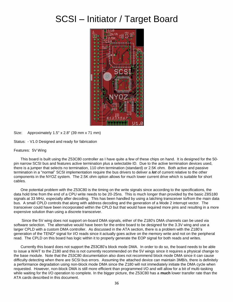
36
SCSI – Initiator / Target Board
Size: Approximately 1.5" x 2.8" (39 mm x 71 mm) Status: - V1.0 Designed and ready for fabrication Features: 5V Wing
This board is built using the Z53C80 controller as I have quite a few of these chips on hand. It is designed for the 50-pin narrow SCSI bus and features active termination plus a selectable ID. Due to the active termination devices used, there is a jumper that selects no termination, 110 ohm termination (standard) or 2.5K ohm. Both active and passive termination in a “normal” SCSI implementation require the bus drivers to deliver a lot of current relative to the other components in the NYOZ system. The 2.5K ohm option allows for much lower current drive which is suitable for short cables.
One potential problem with the Z53C80 is the timing on the write signals since according to the specifications, the data hold time from the end of a CPU write needs to be 20-25ns. This is much longer than provided by the basic Z8S180 signals at 33 MHz, especially after decoding. This has been handled by using a latching transceiver to/from the main data bus. A small CPLD controls that along with address decoding and the generation of a Mode 2 interrupt vector. The transceiver could have been incorporated within the CPLD but that would have required more pins and resulting in a more expensive solution than using a discrete transceiver.
Since the 5V wing does not support on-board DMA signals, either of the Z180's DMA channels can be used via software selection. The alternative would have been for the entire board to be designed for the 3.3V wing and use a larger CPLD with a custom DMA controller. As discussed in the ATA section, there is a problem with the Z180’s generation of the TEND* signal for I/O reads since it actually goes active on the memory write and not on the peripheral read. The CPLD on this board has logic within it to properly generate the EOP signal for both reads and writes.
Currently this board does not support the Z53C80’s block mode DMA. In order to do so, the board needs to be able to issue a WAIT to the Z180 and this is not currently recommended on the 5V wings since it requires a physical change to the base module. Note that the Z53C80 documentation also does not recommend block mode DMA since it can cause difficulty detecting when there are SCSI bus errors. Assuming the attached device can maintain 3MB/s, there is definitely a performance degradation using non-block mode DMA since the Z180 will not immediately initiate the DMA cycle when requested. However, non-block DMA is still more efficient than programmed I/O and will allow for a bit of multi-tasking while waiting for the I/O operation to complete. In the bigger picture, the Z53C80 has a much lower transfer rate than the
ATA cards described in this document.
37
This board started out as a not too serious project just to understand what would actually be required for a basic SCSI
implementation. Over time, this led to a schematic and finally a PCB design. Although this board is fully functional for testing hardware and developing software, there are two shortcomings with it:
1) There is no support to daisy chain the interrupt signal and therefore the board cannot be stacked with other 5V wings that use interrupts.
2) Since this PCB was started mainly as an experiment, the chips and 50-pin SCSI connector were located for relatively short and convenient traces based on a vertical connector. Later when I started thinking about whether the board could be stacked with the Super I/O board, I realized that the connector orientation was rotated 180 degrees from that of a right-angle connector. With the current implementation, there is no electrical or cabling problem when used as a single 5V wing but another board cannot be easily stacked on top of it and the change for a right-angle connector would take a lot of rework.
At this time I do not have any SCSI hard disks with which to test this board, although I do have some SCSI CD drives. If I get serious about testing this board with a hard drive, I will probably just get something like the SCSI2SD module. I know that introduces another layer of software due to emulation, but these kinds of modules are compact, noise free, have no moving parts, only use +5V and don’t require a lot of power. Functional differences in revision levels: V1.0 - First PCB for validation purposes
38
Possible Future Boards
Base Module with an eZ80 - Just thinking about it My original concept for the full system was to have interchangeable Z180 and eZ80 processor modules which would allow for a common physical case and I/O peripherals. Due to the differences in the processors, in addition to significant hardware changes there is a fair amount of unique software development that would be required for this. One option for a development platform would be to create a new eZ80 base module which is compatible with the previously described "wings". The other option, which I'm leaning towards, would be to just create an eZ80 full system using the knowledge gained with the Z180 systems. A lot of the reason for a development system is to experiment with and develop the software for I/O peripherals and to identify their idiosyncrasies. Although there are significant timing differences and internal I/O differences between these two processors, the software development for external peripherals really shouldn't need to be duplicated .

39
Unique Software
There are five main areas of unique code for this system, excluding the MPZ4 board: - Power-on / RESET (i.e. Power On Self Test [POST] code)
This code does the very basic CPU setup and the optional memory testing. The clock divider is configured, refresh is disabled and the initial memory banking is configured. On any RESET, all the general registers are saved so they can be displayed by the monitor; at power-on they are set to 0 and also note that a hard RESET will likewise set the PC, SP, F, I and R registers to zero. At power-on only, the entire main RAM is zero'd; on other RESETs it is left intact for debugging purposes. After this basic configuration is finished, control is transferred to either the resident monitor program or to an operating system (i.e. CP/M), based on a DIP switch input.
- Monitor
This is a basic monitor that allows the user to display/alter registers and memory plus a few other things like breakpoints and basic memory tests, moves and comparisons. This certainly isn't the most compact or "prettiest" code I've ever written as I quickly wrote it many years ago for an entirely different system. However, everything except the LOAD command works as expected and I'd rather concentrate new development efforts towards an efficient BIOS. Entering a "?" gives a list of the supported commands and a CTL-C boots the Operating System. It always uses ASCI 0 at either 9600 or 115,200 baud depending upon a DIP switch input. There are a few unique twists to the monitor in that it detects Output commands to the Z8S180 clock and updates the ASCI 0 serial port configuration accordingly. Likewise, it also detects the enabling of various banks or memory devices and sets any required wait states as appropriate for V1.0 base modules. The monitor must run in Common 1 in order to support both banking and memory shadowing to examine
all attached memory devices (i.e. main RAM, Flash, MRAM and EXT memory). One of the best uses of this monitor is to debug the BIOS, especially the banked version of it. However, the one quirk is that the BIOS cannot overlay the monitor. This means that a BIOS being tested must leave ~5K free at the top of the addressable memory space. For CP/M 2.2, I normally test with CP/M configured for 50KB and Common 1 at C000h which places a roughly 10K BIOS area within Common 1 at C200h. After a hard RESET (power-on or reset switch) the PC and SP registers are always zero'd by the Z180. I know how to resolve this using extra logic but any such development will be deferred to the full system. On this development system the monitor will actually set the saved copy of the PC to 0100h and the SP to a 64-byte stack within the monitor area that is useable by any programs under test. The monitor uses RST 24 (18h or RST 3 in 8080 terms) in order to add breakpoints and the usage of RST 24 should be avoided by any programs to be tested under the monitor. It also provides a rudimentary BDOS function for testing programs using console I/O; Function 1=Console input, 2=Console output, 6=Console I/O and 9=Print string. Programs that use only these BDOS functions can be tested directly under the monitor without the need for, or interaction of a BIOS and/or CP/M. This routine runs with interrupts disabled and uses polled I/O for the console on ASCI 0 which will not affect any interrupt driven queued output to ASCI 0 such as from a BIOS under test. It can be used to debug other interrupt-driven routines but the user should be aware that interrupts will not be serviced while the monitor is in control of the CPU and this may affect things like the BIOS clock. There is currently limited SW/HW support for processing breakpoints when a phantom memory is active and other than the TPA Bank is selected. This could be resolved by defining a Common 0 address space but there would be a lot of implications to the BIOS software and systems such as CP/M-3 or MP/M. Unfortunately
a work-around for some types of external memory (i.e. WIZnet) would be quite difficult on the development system but will be dealt with on the full system.
40
- BIOS Initialization
There are several BIOS functions such as hardware discovery and initialization that are only required one time during a cold boot. Since these are one-time routines with minimal space restrictions (i.e. the full TPA is available), one of their main objectives is to do any processing that can minimize overhead in the runtime routines. The power-on / RESET routine first loads all of the BIOS at 0100h (i.e. TPA) and then transfers to it. One of the first things it does is to re-locate the runtime portions of the BIOS to their actual locations in high and banked memory so they're available as subroutines. This split BIOS concept allows for very simple testing of a new BIOS as a command invokable .COM module and also avoids wasting high memory on routines that are never used after initialization. Sure it adds a bit of overhead, but it appears to the user to be virtually instantaneous. The flexibility makes it well worth the extra CPU cycles during initialization. Because this initialization code has the full TPA available, it can do a lot of pre-testing and configuration in order to optimize the code and data areas for the runtime BIOS depending upon the attached devices. This takes a lot of code and is currently over 9KB of code! A good example of extra initialization code is the discovery of whether serial flash chips exist on an I/O board wing and their subsequent initialization. In a fixed configuration complete system this would only be a validation step. However on a development system, wings may be added or removed and therefore these chips are always optional. If discovered, their type and size must be determined along with whether they have already been formatted into useable "disks". I prefer to handle this in generalized initialization code where a minor code change and re-assembly is only required when support for a new device type is to be added. I have tried as much as possible to make these initialization routines do as much device discovery as practical and then default the identified devices into a useable environment without the need to make source changes and re-assemble the BIOS. Whenever devices are added, the user should carefully note the drive letter assignments at the next power on since they may have changed. Although the CONFIG program can be used to do things like re-order drive letters and alter buffer allocations, the default configuration is quite useable and provides access to most devices. This philosophy and access to devices is important if there is ever a need to restore the system using the base configuration DIP switch when using the MEM-X board or on the full system. Putting these detection and formatting routines into the BIOS initialization code does add a bit of overhead when they're not required. Every reset copies these routines from ROM into RAM before they're actually executed and there is a lot of code that is very seldom used. However, the actual overhead when the routines are not required is only one millisecond for each ~4.65KB of code. On the very positive side, the user does not have to research what utility to use and remember to use it when doing things like adding a MEM-X board or generally when interchanging various wings. These routines can obviously be simplified when used in the full system since there will be much more limited options for expansion and changes. This module also detects the first entry since power-on and automatically formats the RAMdisk(s). This works either on a direct power-on-->BIOS or via a CTL-C from the monitor. There should be no need to reformat the RAMdisk(s) unless there are major bugs in a new program. Even then, a simple ERA *.* usually works or a power off/on will reformat the RAMdisk(s). Due to the ability to create a BIOS as a .COM file, a direct boot from a disk's reserved tracks has not been developed at this time. It really isn't required but it would allow for flexibility and allow a new BIOS to be hidden in the reserved tracks. One difficulty will be the suppression of the built-in BIOS's messages which should only be displayed if a disk-based BIOS is not found. If this is implemented in the future, due to the quick load of the built-in BIOS it will probably be done as a two stage loader: 1) Boot the built-in BIOS for full I/O access to all "disks" - There would be no need for a cold start loader on track zero sector one 2) Check for a disk-based BIOS based on a DIP switch option The actual format of the hidden disk-based BIOS would be the same as other BIOS's (i.e. load at 100h). However, it would probably require a slight change to identify it. For example:
41
JR $+7 ; Beginning loaded at 100h DB 'BS' ; Signature DB ? ; Starting track DB ? ; Starting sector DB ? ; Count of 512 byte sectors
- BIOS Runtime Routines
These are the routines required by the operating system (i.e. CP/M) during execution for console access, "disk" access etc. At this time, it mostly runs within Common 1 and future enhancements will move much of the code into a bank area. That will allow the size of the BIOS in the basic memory map to be reduced which then increases the size of the TPA. It would also create the option to reduce the size of Common 1 and also allow the size of any banked TPA to be increased (currently 48KB). The actual I/O within these routines is mostly interrupt driven and relies on the fact that interrupts are not nested. Routines which require more than simple processing just set an interrupt-occurred flag and defer more exhaustive analysis to the task waiting for the interrupt, thus minimizing interrupt disabled time. There is a unique stack area for the BIOS routines in the common data area so only one stack entry (return address) is used on the caller's stack. Likewise, there is also a unique stack for the interrupt routines. Note that the current interrupt routine implementation uses the alternate register set (i.e. AF', BC', DE' and HL') for quick entry / exit while preserving register contents. If ZCPR is implemented or any user programs uses the alternate register set then a change will need to be made to the interrupt entry / exit macros. It should be noted that the interrupt vector must be on a 64-byte boundary (IL register bit 5 equal zero) and it is highly recommended that the vector actually be on a 128-byte boundary to allow for future expansion. The CP/M 2.x IOBYTE function has been implemented in the base system which allows for testing various devices by first using a known good interface as set by the DIP switches or CONFIG utility and then re-assigning it using the STAT command (i.e. STAT CON:=CRT:). If a device is not defined then input will always return a CTL-Z and output will simply be discarded. The following devices are currently implemented or planned for:
TTY: - ASCI0 CRT: - P8X32A keyboard / video UC1: - ASCI1 RDR: - ASCI1 PUN: - ASCI1 LPT: - Printer on Super I/O card (future enhancement) UR1: - FT232H High speed USB UP1: - FT232H High speed USB UR2: - VNC II Port 1 USB (future enhancement) UP2: - VNC II Port 1 USB (future enhancement) UL1: - Printer attached to VNC II port 1 (future enhancement)
- Unique Utilities
Most of the supplied utilities were primarily written for testing purposes. As such, they don't always do full error checking and there may even be a few bugs or quirks in them. The user interface is functional but certainly not anything special ... just basic TTY style displays and input. Some of them have snippets of very old code from other systems so the coding style may also appear to be somewhat inconsistent. In general, they always ask for confirmation before altering anything significant.
CLOCK - Display BIOS clock CLS - Clear the screen like the DOS command CONFIG - Modify configuration data in EEPROM (still being enhanced) DATE - Display [set] Real Time Clock (RTC) date (also updates BIOS clock)
42
PCGET - Receive a file via XMODEM or XMODEM-1K on ASCI 1 PCPUT - Send a file via XMODEM or XMODEM-1K on ASCI 1 (future) TESTEE - Test then restore or zero EEPROM data. - Zeroing will effectively reset all configuration options to defaults TESTI2C - Test (i.e. read or write) I2C devices TESTMEMX - Test all the RAM and MRAM on a MEM-X board TESTRST - Test the trapping of an uninitialized RST at 0100h TESTTRAP - Test the trapping of an invalid instruction at 0100h TIME - Display [set] RTC time (also updates BIOS clock) TOD - Display [set] RTC date [and time] (also updates BIOS clock)
There are a few utilities and files that are unique to the MPZ4 multi-processor board. The ones that are loaded by SLVLOAD into an MPZ4 board have a special prefix in the code and a default extension of '.SLV'. If an appropriate CP/M system is loaded into the MPZ4 this way, it can then use normal .COM programs.
SLVCPM58.SLV - A 58KB CP/M 2.2 system with BIOS, monitor and a 440KB RAMdisk SLVCPM63.SLV - A 63KB CP/M 2.2 system with BIOS and a 440KB RAMdisk - No access to base module disks at this time SLVLOAD - Inject POST routine, basic loader and .SLV files into one or more MPZ4
slaves - Used to load application programs and/or data SLVMON.SLV - Just the debug monitor
SLVRAMD - Create a slave loadable RAMdisk image of the base module's RAMdisk SLVTEST.SLV - Tests the loader, slave memory, LEDs and timing (1Hz digits)
The default operating system that is loaded into the base module at RESET is a clean CP/M 2.2 system with only the required Digital Research patches applied. However, the configuration utility allows the user to specify an "AUTOEXEC" type of command which can be used to automatically invoke a different BIOS and/or operating system such as CP/M 3 or MP/M. By setting the "QUIET" option in the CONFIG utility, unless there are hardware errors detected, the first message on the console is from the alternate BIOS or operating system. Future updates may allow these different operating systems to be embedded in flash memory and invoked directly. In the meantime, the CP/M 2.2 system can simply be used as a loader for a different operating system. The startup of a memory-disk only version of the base module and loader is so quick that the user won't perceive the overhead. Note that there is a DIP switch option to over-ride and inhibit any "AUTOEXEC" and forces the basic (i.e. loader) CP/M system to remain as the active operating system. BANKing Warning:
Normal application programs in the TPA should not have any need to directly implement banking (i.e. altering the BBR register). However, certain utilities may need to do so. Because the interrupt hardware will stack the return address before the interrupt routine can switch to it's unique stack, any routine operating in the TPA that uses banking must either disable interrupts or have a stack pointer within Common 1 in order to prevent a one word overlay if an interrupt occurs. These routines can use the highest part of the Common 1 TPA (256 bytes pointed to by $C1_TPA) for a stack with interrupts enabled so long as they make allowance in overlay routines for their own stack requirements plus an extra word for an interrupt return address.
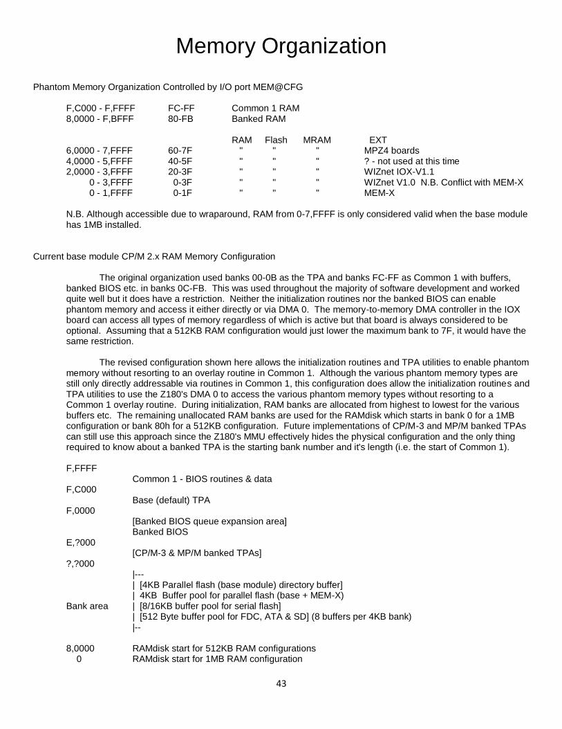
43
Memory Organization
Phantom Memory Organization Controlled by I/O port MEM@CFG F,C000 - F,FFFF FC-FF Common 1 RAM 8,0000 - F,BFFF 80-FB Banked RAM RAM Flash MRAM EXT 6,0000 - 7,FFFF 60-7F " " " MPZ4 boards 4,0000 - 5,FFFF 40-5F " " " ? - not used at this time 2,0000 - 3,FFFF 20-3F " " " WIZnet IOX-V1.1 0 - 3,FFFF 0-3F " " " WIZnet V1.0 N.B. Conflict with MEM-X 0 - 1,FFFF 0-1F " " " MEM-X
N.B. Although accessible due to wraparound, RAM from 0-7,FFFF is only considered valid when the base module has 1MB installed.
Current base module CP/M 2.x RAM Memory Configuration
The original organization used banks 00-0B as the TPA and banks FC-FF as Common 1 with buffers, banked BIOS etc. in banks 0C-FB. This was used throughout the majority of software development and worked quite well but it does have a restriction. Neither the initialization routines nor the banked BIOS can enable phantom memory and access it either directly or via DMA 0. The memory-to-memory DMA controller in the IOX board can access all types of memory regardless of which is active but that board is always considered to be optional. Assuming that a 512KB RAM configuration would just lower the maximum bank to 7F, it would have the same restriction. The revised configuration shown here allows the initialization routines and TPA utilities to enable phantom memory without resorting to an overlay routine in Common 1. Although the various phantom memory types are still only directly addressable via routines in Common 1, this configuration does allow the initialization routines and TPA utilities to use the Z180's DMA 0 to access the various phantom memory types without resorting to a Common 1 overlay routine. During initialization, RAM banks are allocated from highest to lowest for the various buffers etc. The remaining unallocated RAM banks are used for the RAMdisk which starts in bank 0 for a 1MB configuration or bank 80h for a 512KB configuration. Future implementations of CP/M-3 and MP/M banked TPAs can still use this approach since the Z180's MMU effectively hides the physical configuration and the only thing required to know about a banked TPA is the starting bank number and it's length (i.e. the start of Common 1).
F,FFFF Common 1 - BIOS routines & data F,C000 Base (default) TPA F,0000 [Banked BIOS queue expansion area] Banked BIOS E,?000 [CP/M-3 & MP/M banked TPAs] ?,?000 |--- | [4KB Parallel flash (base module) directory buffer] | 4KB Buffer pool for parallel flash (base + MEM-X) Bank area | [8/16KB buffer pool for serial flash] | [512 Byte buffer pool for FDC, ATA & SD] (8 buffers per 4KB bank) |-- 8,0000 RAMdisk start for 512KB RAM configurations 0 RAMdisk start for 1MB RAM configuration

44
Current boot flash configuration 1,0000 - ? ROM "disk" - N.B. 64KB offset EA00 - FFFF CP/M 2.2 50K image 2000 - ? BIOS (N.B. loader prefix) 0-1FFF Z180 + WSMMON + some expansion space Current base module MRAM configuration 1,0000- ?? - MRAM "disk" 4000-FFFF - Serial flash tables - 128 MB total serial flash 4000-BFFF - " ” " - 64 MB 4000-7FFF - " " " - 4 MB to 32 MB 1000-3FFF - Parallel flash tables (future enhancement); max 8MB w/ 4K sectors) 800-0FFF - Parallel flash control area (future enhancement) 80-07FF - Serial flash control area 0-007F - RST code duplication area for breakpoints N.B. 64 KB of MRAM space always reserved on development system to allow for different wings. Current Serial Flash low data areas 1000-CFFF - 128 MB checkpoint; data starts at 1,0000 1000-6FFF - 64 MB " 8000 1000-3FFF - 32 MB " 4000 1000-27FF - 16 MB " " 1000-1BFF - 8 MB " " 1000-15FF - 4 MB " " ???-0FFF - unused 0-0??? - Serial flash control area checkpoint

45
I/O Map
N.B. These are the generic address ranges for the V1.1+ base modules and the wings that have been developed at this time. The individual addresses and their bit definitions should be checked in the source copy member "IO_MEM.cpy" since it contains the actual definitions that are used for the BIOS assemblies. The code will always reflect the up to date definitions for the various board and CPLD revision levels. All of the I/O addresses are decoded as 8-bits only so that "IN A,(port)" and "OUT (port),A" can be used. Note that Z180 internal I/O registers are always accessed using the IN0 and OUT0 instructions since they're treated as 16-bit I/O addresses and need the high byte of the address to be zero. These Z180 registers can also be accessed by the TSTIO instruction, IN/OUT (C) if register B=0 or the new Z180 block output instructions (OT [I|D] M [R] ) since they output zero on the upper address byte. Many of the older CP/M programs that allow I/O instructions are based on the 8-bit only 8080 and there are potential conflicts when accessing the Z180 internal I/O registers which are 16-bit. This is definitely an issue with the MBASIC5 INP and OUT functions and I have seen some debug monitors that also have this issue. 00-3F : Z8S180 Internal registers 40-4F : MAIN CPLD on IOX board 50-5F : SD card CPLD on IOX board 60-63 : Parallel port ECP registers on Super I/O board 64 : FDACK* on Super I/O board 65 : PDACK* on Super I/O board 66-67 : PC87334 Index / Data on Super I/O board 68-6F : Parallel port on Super I/O board 70-77 : UART2 on Super I/O board 78-7F : UART1 on Super I/O board 80-8F : ATA board " - also used by the mutually exclusive ATA-F board 90-9F : I/O CS* on 5V wing – not used at this time 90-98 : Flash Programmer board 98-9F : IDE (Primary) on Super I/O board (disabled) 99 : SCSI ID port 9A : SCSI DMA Selection 9B : SCSI DMA I/O 9E : FDC interrupt mask 9F : FDC & LPT DMA configuration (in CPLD) A0-AF : I/O CS* on 3.3V wing - used by MEM-X board (V1.0 = A0-AF, modified or V1.1+ = A0-A7) - used by MPZ4 boards - A8-AF B0-B7 : SCSI card Z53C80 B8-BF : FDC (Primary) on Super I/O board C0-CF : Serial flash CPLD on IOX board D0-EF: ATA board " - also used by the mutually exclusive ATA-F board F0-FF : System CPLD on the base module N.B. E0-EF are also used by the Z80181
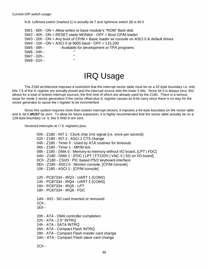
46
Current DIP switch usage: N.B. Leftmost switch (marked 1) is actually bit 7 and rightmost switch (8) is bit 0
SW1 - 80h - ON = Allow writes to base module's "ROM" flash disk SW2 - 40h - ON = RESET starts MONitor - OFF = Boot CP/M loader SW3 - 20h - ON = Any boot of CP/M = Basic loader w/ console on ASCI 0 & default drives SW4 - 10h - ON = ASCI 0 at 9600 baud - OFF = 115,200 SW5 - 08h - Available for development or TPA programs SW6 - 04h - " SW7 - 02h - " SW8 - 01h - "
IRQ Usage
The Z180 architecture imposes a restriction that the interrupt vector table must be on a 32-byte boundary i.e. only bits 7-5 of the IL register are actually preset and the interrupt source sets the lower 5 bits. Since bit 0 is always zero, this allows for a total of sixteen interrupt sources, the first nine of which are already used by the Z180. There is a serious issue for mode 2 vector generation if the vector offset plus IL register causes an 8-bit carry since there is no way for the vector generator to cause the I register to be incremented. Since this system requires more than sixteen interrupt vectors, it imposes a 64-byte boundary on the vector table and IL bit 5 MUST be zero. To allow for future expansion, it is highly recommended that the vector table actually be on a 128-byte boundary i.e. IL bits 5 AND 6 are zero. Vectored interrupts at I / IL registers plus:
00h - Z180 - INT 1 : Clock chip 1Hz signal (i.e. once per second) 02h - Z180 - INT 2 : ASCI 1 CTS change 04h - Z180 - Timer 0 : Used by ATA routines for timeouts 06h - Z180 - Timer 1 : MP/M tick 08h - Z180 - DMA 0 : Memory-to-memory without I/O board, [LPT | FDC] 0Ah - Z180 - DMA 1 : [FDC | LPT | FT232H | VNC II | SD on I/O board] 0Ch - Z180 - CSI/O : PIC based PS/2 keyboard interface 0Eh - Z180 - ASCI 0 : Monitor console, [CP/M console] 10h - Z180 - ASCI 1 : [CP/M console] 12h - PC87334 - IRQ3 - UART 1 (COM2) 14h - PC87334 - IRQ4 - UART 2 (COM3) 16h - PC87334 - IRQ5 - LPT 18h - PC87334 - IRQ6 - FDC 1Ah - XIO - SD card inserted or removed 1Ch - 1Eh - 20h - ATA - DMA controller completion 22h - ATA - 2.5" INTRQ 24h - ATA - SATA INTRQ 26h - ATA - Compact Flash INTRQ 28h - ATA - Compact Flash master card change 2Ah - ATA - Compact Flash slave card change 2Ch -

47
2Eh – SCSI – Z53C80 30h - XIO - WIZnet 32h - XIO - FT232H - data available to read 34h - XIO - VNC II - data available to read 36h - XIO - P8X32A - okay to write video data 38h - XIO - P8X32A - keyboard data available 3Ah - XIO - P8X32A - mouse data available 3Ch - XIO - VNC II - okay to write data 3Eh - XIO - FT232H - okay to write data 40h - MPZ4 - Board 0 requesting service 42h - MPZ4 - " 1 " " 44h - MPZ4 - " 2 " " 46h - MPZ4 - " 3 " "
Hex Display and Error Beep Codes
During power-on or reset initialization / testing, the MONitor routine execution and BIOS initialization, there are various LED display codes and possibly error beeps. Just before passing control to the Operating System after a RESET, the LED display is blanked. The display is then available for use by application programs as may be required. Note that all the following codes are hexadecimal as displayed on the LEDs. Reset routines FF + 5 beeps followed by HALT - Invalid instruction (i.e. TRAP) within the RESET code F0 + 4 beeps followed by HALT - Memory error in Common 1 memory testing ?? + 3 beeps followed by HALT - Memory error in bank memory testing: ?? = BBR 08, 10, 18, 20, 28, 30 or 38 plus 5 beeps followed by HALT - Unexpected RST instruction executed within the RESET code 66 + 5 beeps followed by HALT - Unsupported NMI during RESET initialization FE - Start of normal RESET routine FD - RESET routine entered as a result of a MON memory test FC - Crystal option has been set FB - Wait states set, refresh disabled and bank registers initialized FA - Registers saved for MON F9 - Before Common 1 memory test F8 - Return from Common 1 memory test F7 - Before Common 0 and bank area memory tests / zeroing F6 - Return from Common 0 and bank area memory tests / zeroing F5 - Start of search for a boot routine to load F4 - Boot routine found and before copying it to RAM F3 - Boot routine has been copied to RAM F2 - Just before transferring to boot routine
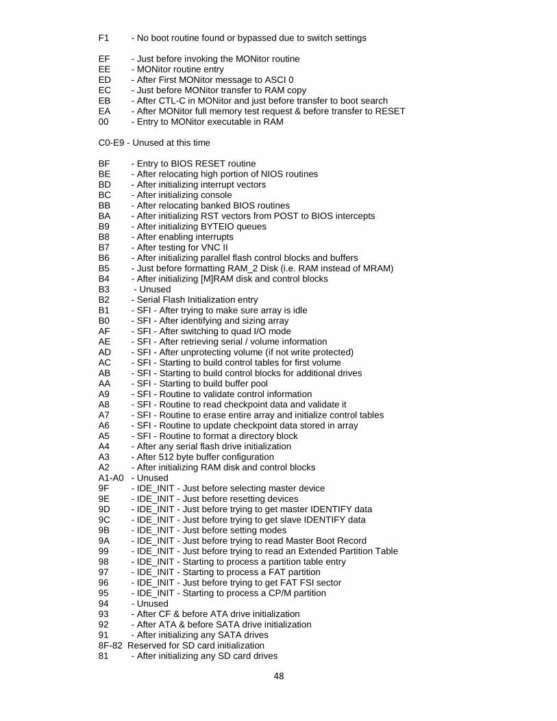
48
F1 - No boot routine found or bypassed due to switch settings EF - Just before invoking the MONitor routine EE - MONitor routine entry ED - After First MONitor message to ASCI 0 EC - Just before MONitor transfer to RAM copy EB - After CTL-C in MONitor and just before transfer to boot search EA - After MONitor full memory test request & before transfer to RESET 00 - Entry to MONitor executable in RAM C0-E9 - Unused at this time BF - Entry to BIOS RESET routine BE - After relocating high portion of NIOS routines BD - After initializing interrupt vectors BC - After initializing console BB - After relocating banked BIOS routines BA - After initializing RST vectors from POST to BIOS intercepts B9 - After initializing BYTEIO queues B8 - After enabling interrupts B7 - After testing for VNC II B6 - After initializing parallel flash control blocks and buffers B5 - Just before formatting RAM_2 Disk (i.e. RAM instead of MRAM) B4 - After initializing [M]RAM disk and control blocks B3 - Unused B2 - Serial Flash Initialization entry B1 - SFI - After trying to make sure array is idle B0 - SFI - After identifying and sizing array AF - SFI - After switching to quad I/O mode AE - SFI - After retrieving serial / volume information AD - SFI - After unprotecting volume (if not write protected) AC - SFI - Starting to build control tables for first volume AB - SFI - Starting to build control blocks for additional drives AA - SFI - Starting to build buffer pool A9 - SFI - Routine to validate control information A8 - SFI - Routine to read checkpoint data and validate it A7 - SFI - Routine to erase entire array and initialize control tables A6 - SFI - Routine to update checkpoint data stored in array A5 - SFI - Routine to format a directory block A4 - After any serial flash drive initialization A3 - After 512 byte buffer configuration A2 - After initializing RAM disk and control blocks A1-A0 - Unused 9F - IDE_INIT - Just before selecting master device 9E - IDE_INIT - Just before resetting devices 9D - IDE_INIT - Just before trying to get master IDENTIFY data 9C - IDE_INIT - Just before trying to get slave IDENTIFY data 9B - IDE_INIT - Just before setting modes 9A - IDE_INIT - Just before trying to read Master Boot Record 99 - IDE_INIT - Just before trying to read an Extended Partition Table 98 - IDE_INIT - Starting to process a partition table entry 97 - IDE_INIT - Starting to process a FAT partition 96 - IDE_INIT - Just before trying to get FAT FSI sector 95 - IDE_INIT - Starting to process a CP/M partition 94 - Unused 93 - After CF & before ATA drive initialization 92 - After ATA & before SATA drive initialization 91 - After initializing any SATA drives 8F-82 Reserved for SD card initialization 81 - After initializing any SD card drives

49
80 - Unused 7F - After initializing FT232H 7E-7B Unused 7A - VNC II Initialization - Pass 1 79 - VNC II Initialization - Pass 2 entry 78 - VNC II Init - Pass 2 after prompt found 77 - VNC II Init - Pass 2 after switch to short commands 76 - VNC II Init - Pass 2 after switch to monitor in binary 75 - VNC II Init - Pass 2 after query for BOMS "disk" present 74 - VNC II Init - Pass 2 after mount of BOMS "disk" 73 - VNC II Init - Pass 2 after enabling unsolicited event interrupts 72 - VNC BOMS capacity calculation during CONFIG 71 - After initializing VNC II and any VDAP BOMS drive 70 - 6F - After possibly changing drive letters and messages in CONFIG 6E-62 Reserved for LOAD_CPM 61 - After loading CCP & BDOS 5F - After optional CP/M information message(s) 5E-52 Reserved for clock routines 51 - After successfully retrieving date and time, just before OPS blank - Just before transferring to CBOOT routine A very few of the various service routines may also display an error code during runtime. Serial Flash AA - Physical block allocation error AB - " " " " Decimal point LED's from left to right: DEC3 - Toggled at entry to one second clock routine (i.e. flash at 0.5 Hz) DEC2 - Toggled at entry and exit of MRAM disk I/O routine DEC1 - Toggled at entry and exit of RAM disk I/O routine DEC0 - Toggled at entry and exit of ROM (flash) disk I/O routine The Serial flash disk on the IOX board has a dedicated LED indicating access and likewise for each of the ATA, CF and SATA interfaces on the ATA boards.

50
Zilog Z80 Family and Derivatives Everyone has their own opinions about what constitutes a good microprocessor and it is often biased by the series they are most familiar with. Here are a few of my thoughts about the various Zilog processors.
Z80 Obviously this is the chip that started Zilog's microprocessor activities and I chose it over the 8080 in the mid 1970's after carefully comparing the two. Originally it was developed in NMOS (i.e. power hungry) and later became available in CMOS (which I much prefer). I have no real issue with the actual processor chip and it's 1970's roots certainly advanced the whole microprocessor scene. However, there is an issue if one is trying to build an enhanced system utilizing support chips from this family (i.e. serial I/O, DMA, parallel I/O etc.). Each of these chips is available in different speed ratings but the maximums are all different. The CPU tops out at 20Mhz, DMA at 8MHz, and the CTC, PIO and SIO max out at 10MHz. There are also a few integrated peripherals such as the KIO at 12.5 MHz whereas some of the useful homebrewing chips like the DART are not available in CMOS. Given the range of speeds, the designer really needs to consider whether a design will ever be expanded and what the maximum speed and configuration will be before selecting components, including support devices. In comparison to the Z180 there can possibly be a lot of "glue" logic and the final system is limited to 64KB unless there is extra logic in the "glue". The issue I have with external logic implementing functions like banking is that every design is very likely different and the software is not portable without changes. Now that I've talked about the negatives, I'll also say that I do find a place for the basic Z80 in embedded applications where the designer is basically looking for a CPU core plus maybe just one peripheral like the SIO. The memory size and overall speed is usually not an issue in these applications. Very early example of this concept appeared in S100 support cards such as floppy disk interfaces (i.e. Jade DD) and video cards (i.e. SD's VDB8024) where a Z80 was used as an embedded I/O processor to offload the main processor from repetitive things like timing loops, screen scrolling etc. However, in the 21st century there are much more integrated and cost-effective solutions for embedded designs that include all the required support circuitry within a single chip. Zilog actually produced a few variants of the Z80 to fill the embedded niche. For me, I find the Z80C13 which they called an Intelligent Peripheral Controller to probably be the most useful as it includes the Clock Generator Controller, a four channel CTC and a two channel SIO. The Z80C15 has similar features plus two 8-bit PIO ports. For the neophyte designer that is not worried about speed or expandability, the NMOS versions of the Z80 can be a good starting point. In my experience, they are quite robust and tolerant of design errors, especially when used with 74LSxxx support chips, whereas CMOS is more sensitive and the higher speeds can get trickier. These chips are available relatively cheaply and the designer can learn about various issues that are common to all microprocessors: i.e. data and address buses, address decoders, interrupt chaining etc.
Z180 (HD64180) This is my current favourite and first choice within the Z80 family and the reasons are pretty simple. It has integrated I/O (MMU, DMA, serial, timer) a relatively large address space (1MB) and is easily interfaced to other devices. A very flexible and expandable CP/M system can be built with just four chips (Z180, flash, SRAM and decoder) plus a few discrete components ... a possible fifth chip might be an RS-232 transceiver. Pretty simple and quite powerful. With it's integrated MMU, this chip creates a good foundation for a banked system such as CP/M-3 or MP/M and has also been used in the past for the development of alternative operating systems such as UZI180. The Z180 should be object code compatible with most Z80 programs. Obviously there may be differences in programs that directly access I/O ports and any banking activities should be transparently handled by the BIOS and/or operating system. There are three subtle instruction differences between the Z80 and Z180 and these relate to the RLD, RRD and DAA (after a DEC) instructions. These are not likely to impact most programs. The original Z80180 is available in speeds up to 10MHz while the Z8S180 version goes up to 33MHz. Unfortunately the "S" version has some published errata that the designer needs to be aware of ... not a big deal if one is aware of them but definitely a potential "gotcha". I have implemented several designs with the "S" version without any
51
significant difficulty. Early in the development of the "S" version there were two versions with a very significant difference and there was also an original version that was not full featured. Chips dated 99 and later that aren't marked as 'SL1960" should be okay and are available from many sources.
eZ80 This chip is the logical upwards migration path from the Z180 and contains more support devices (I/O and memory), a faster core plus support for 24-bit addressing (i.e. 16MB). While Z80 application code may be upwards compatible with this device, there will be considerable effort required to create a compatible operating system (or BIOS) that fully utilizes all the new features. When one looks at the various other Zilog processors, this one appears to be like a merging of the Z280 and Z380 plus extra support peripherals. It is the most advanced Zilog chip of the Z80 derivatives that is in production today and it's internal memory and I/O plus the overall speed (potentially equivalent to about a Z80 at 200MHz) make it very worthy of consideration for the foundation of a complete system.
Z280 This chip showed great promise when it was originally released but it's development and production was discontinued. The key identifying features were a 24-bit address space (i.e. 16MB), program/supervisor modes and enhanced integrated peripherals (i.e. four DMA channels). It could certainly be used as the foundation of a very useful system. Unfortunately, it is my understanding that this device also contains several hardware "bugs" that were never resolved in hardware.
Z380 Although this chip made it into production, I don't believe it ever really caught on. In reviewing the documentation, the only real noteworthy features that I see are a 32-bit address space (i.e. 4GB), 32-bit registers and the extra sets of registers. From a designer standpoint, there needs to be a full complement of external peripherals in order to make a complete system. If it had a very significant speed advantage then this might have been worth the extra development effort but in reality it was only 18MHz, albeit instructions cycles had been reduced. Without going through the exact cycle counts, at it's two cycle minimum it is probably about the same effective speed as a 33MHz Z8S180.
Z800
This was basically an NMOS version of the chip that was later delivered as the Z280 in CMOS. It was only available for a very short time and to the best of my knowledge never achieved any level of commercial success.
Z8000 (Z16C00 ?) This was Zilog's solution for a 16-bit microprocessor but it never gained a lot of popularity once IBM selected the 8088 for the PC. It was also introduced at about the same time as the MC68000 was gaining popularity. From a programmer's standpoint, I think this device could be an extremely useful foundation for a system since it could address up to 48MB, had lots of extra registers, user/system modes, etc. However, that same advantage was also a negative since it was not object-code compatible with the Z80. Besides the requirement for a unique operating system (CP/M was never commercially ported so far as I remember), every application program would also have required both a Z80 and a Z8000 version.
Z80000 This was Zilog's solution for a 32-bit processor and upwards compatible with the Z8000. Although the preliminary Product Specification manual is available, not a lot of other details are generally available.
52
CPLD vs. FPGA Complex Programmable Logic Devices vs. Field Programmable Gate Arrays I like to use CPLDs for the logic functions in boards like these since they're compact, fast, very flexible and simplify the hardware design from using multiple chips with larger board layout to just programmable logic that can easily be changed. They can also be much cheaper than discrete logic when one adds chip costs, board area, PCB layout effort, redesign costs etc. I no longer use PALs/GALs/PLDs since I find them too restrictive, relatively slow and very power hungry. I did use a few discrete logic chips on the base module but this was done to meet tight timing requirements without going to a faster and much more expensive CPLD. On some of the other boards I used a few discrete logic chips in order to reduce the CPLD pin count and avoid going to a larger and more expensive device. Opinion:
FPGAs could have been used instead of CPLDs in this design. However, a lot of the required logic is asynchronous discrete functions with many inputs and there is no need for the advanced features found in FPGAs. I find that CPLD logic is easy to understand, has simple deterministic timing for this purpose and can actually be faster than FPGAs for wide logic functions such as fully decoded I/O selects. Having said that, I also believe that FPGAs are a much better choice for block I/O interfaces like SD and ATA where one needs to interface the system to devices with very different timing requirements. The use of an FPGA with DMA and FIFO buffers makes much more efficient use of the system's bus bandwidth in those cases.
Sidenote:
I am aware of the many cautionary statements made about the use of HDL's (Hardware Description Languages) by software programmers who are used to working with linear programming languages. Perhaps it’s because of my background with discrete logic design or the fact that most of my software background is with true multi-tasking at the assembly level, but so far I haven't had any issues with this. I find that I choose to develop related logic functions at the same time and keep in mind what else could be happening asynchronously. I'll also admit that I tend not to create a lot of test vectors and exhaustive simulation scenarios during my development. Instead, I try to fully understand the related logic through careful analysis before writing the HDL code. Although I've found a few issues that required further analysis and correction, so far I've been very successful in only requiring the oscilloscope and/or a logic probe to validate these functions rather than needing a logic analyzer for serious debugging.
My CPLD family of choice is Xilinx's CoolRunner series as they have most of the features I require and I had originally started working with them when they were developed by Philips before being acquired by Xilinx. This series uses negligible static power and much less dynamic power than most other families. The 3.3V XPLA3 series (i.e. XCR3...) work very well to interface between 5V and 3.3V logic since the inputs are 5V tolerant and the outputs are TTL compatible. The CoolRunner II series (i.e. XC2C...) cost less and have some nice extra features but require a 1.8V supply and only interface to 3.3V or lower. The major disadvantage for hobbyists is that these devices are now only available in solderable packages such as QFP, CSP and BGA. It is worthwhile to note that the next larger devices (more macrocells) within the same family and package are usually pin compatible and I sometimes use this feature due to availability or when I find cheaper deals on the larger devices (yes it happens). I always do my development based on the smaller device to verify that it can still contain the design before changing the device type to a larger one. Sometimes due to the board routing using unused pads on the smaller devices as pass-throughs, this may require a change to the constraints file to ensure that I/O pins in the larger devices are floating rather than having a weak pullup. Through the years I've worked with various programmable logic software packages such as PALASM, CUPL, MachXL, etc. and some more recent packages such as Xilinx ISE, Lattice ispLEVER etc. Just like I prefer to use assembly language for low-level software, I have found that I prefer to use ABEL (or something similar) as my HDL language of choice when working with PLDs or CPLDs. It clearly defines the required logic function without a lot of verbose ambiguity. I also understand that Verilog and VHDL are better languages for FPGAs that contain considerably more logic, multiple instances of functions etc. Unfortunately, Xilinx chose to drop ABEL as a supported language many years ago (2009?) and the last version of ISE to support it was V10.1. I run a copy of ISE 10.1 under Windows XP but I am definitely not impressed with this
package. In my opinion, this package epitomizes bloated GUI software where the developers want an all-inclusive end-all be-all package. My copy of V10.1 is roughly 4.5GB in size with over 79,000 files and that is before including about three hundred files it creates for each unique project!!! More importantly, I have experienced aborts back to Windows and
53
inconsistent detection of changes that should require design steps to be re-executed. My copy of V13.1 is 12.6GB with over 170,000 files. Another prime example of bloatware is the .IPF file it creates to describe the device to be programmed ... 21KB plus registry entries to basically just record the device type, filename and a few options such as cable type ... ouch! Moreover, that was for the smallest and only XCR device on a JTAG chain. The good news is that ISE V10.1 supports the various devices that I use and I can usually generate acceptable results.
On my main Windows 7 system I also have a more recent copy of the ISE tools (i.e. IMPACT) which I use when programming these devices. I know it's downlevel but the current version I'm using is 13.3_1 and it seems to be quite efficient. Since I already had the cable and port available, I still use the parallel cable and it has worked flawlessly for me. What I have not tried at this time is to use V10.1 to convert the ABEL source to VHDL or Verilog and then import the result into a more recent version of ISP for the fitting step. From a functional standpoint, the biggest problem I have with ISE relates to it's various optimizers, especially when a larger device with significant logic exceeds perhaps 80% utilization and I'm trying to upgrade it. The optimizers sometimes do a great job of simplifying complex logic but in doing so they also sometimes hinder the ability of the user to actually control the result. Sure there are various options (way too many in my opinion) but each requires a tedious iteration and a very careful check of the results. I have spent many hours (days?) with one particular issue on several designs while trying to get the optimizers to not reduce a particular type of equation since I'm trying to use them as a timing delay. All the obvious options such as KEEP, RETAIN, NOREDUCE, .PIN, LOGIC_OPT OFF, etc. appear to work and then the fitter's optimizer eventually ignores them without warning. After many hours on this simple task, it appears the only way to consistently handle it might be to either re-code the entire source with various optimized logic (much harder to read/understand) and then prevent all ISE optimization (i.e. WYSIWYG) or to route these equations out one physical pin and back in through another pin (not practical in pin-limited designs). I've spent countless hours on another design where the fitter chose to split a critical equation until I finally figured out how to forcefully split a different non-critical equation and circumvent the issue. I have also had instances with ISE's fitter where I can see there is an obvious technique to get unplaced logic into a Function Block / Macrocell but the fitter cannot seem to find it ... very frustrating and a total waste of my time as I iterate on the options to force the required assignments. Interestingly, I have never seen the optimizers use the fold-back NAND option even though I believe there were instances where it might have been useful. Perhaps that is because the CoolRunners were originally designed by Philips and are the only Xilinx device to incorporate this feature. If it wasn't for the fact that I like the underlying devices (i.e. CoolRunners), I would NOT use this software package. My objective is to design and test circuits, not to spend endless hours trying to understand the idiosyncrasies of a software package. Tip:
Whenever ISP gives a warning message, especially in the fitter, it should be carefully investigated. Sometimes the root cause is not obvious but the effects (i.e. buffering signals which creates additional delays) can be VERY significant.
In contrast to ISE, I have spent a bit of time with Lattice's ispLEVER to investigate migrating a design to the ispMACH 4000 family. The version of ispLEVER that I used (V1.7) fully supports ABEL but there are a few differences in how it handles ranged variables compared to ISE. I also had it abort a few times and it even forced me to restart Windows several times due to hidden tasks it spawned that went into endless loops. What really amazed me was it's speed. When first using the package, I had to very carefully check that it actually produced the required output files since it ran virtually instantaneously when compared to Xilinx's extremely slow ISE. From a device perspective, the ispMACH 4000 family only has 36 inputs to a Generic Logic Block (16 Macrocells) versus the 40 inputs to a CoolRunner Function Block (16 Macrocells) and 54 inputs to a XC9500 Function Block (18 Macrocells). I've found that my designs usually have a few logic functions that require a lot of inputs and this can become an issue if the logic starts to expand after the board has been routed and pin locked since this can lead to fitter problems. I tend to limit the Function Block fan-in during initial development and leave at least one unused Function Block input but that doesn't always resolve future issues. I have one design where I used this technique and everything worked well until I expanded one equation and it required one more input. Regardless of ISE's options, when I allowed it to use the extra Function Block inputs it could not fit the design without splitting / layering other equations. Without pin locking, the design fits fine so that only left the option of either accepting delays in other parts of the logic or altering the board layout. Caution:
Although CPLDs allow a lot of layout freedom and choice in the use of pins, there are some caveats. I've found that one should pay extra attention to the pins versus function blocks when selecting pins for things like the data bus, especially in larger designs. The potential problem is the fan-in to the function block can become excessive
54
which results in having to create intermediate nodes as buffers or multiplexers. While this can be done if there are spare macrocells, my experience has been that the fitters don't do a good selection job unless one adds timing constraints and it can become a very time consuming iterative manual process. An alternative option, which I'd recommend, is to first run the fitter without pin constraints and check to see how it tries to balance the I/O pins and function block inputs. This will show which equations and pins require a large fan-in that is not shareable with other macrocells in a function block and can then be used for a more optimal balanced CPLD layout. The data bus to function block mapping also has a possible undesirable effect due to simultaneous switching of outputs. Likewise for things like address busses in DMA controllers. That is another issue but I'm not going to delve into it here.
Although I've used CPLDs in several different projects, I really haven't spent a lot of time with FPGA's other than my research. I do understand most of the concepts including things like the Wishbone interface and have studied a lot of data sheets. In particular, I really like the idea of dual-ported FIFO RAM blocks for interfaces between various devices with different data transfer speeds. Although it hasn’t been fabricated and tested, I have redesigned and completed the layout of the ATA board to use a Microsemi ProASIC3 FPGA. I liked their instant-on capability due to flash configuration and I managed to acquire several of the 250K gate devices at a very reasonable cost. As this project evolves I'll be in a better position to review whether this was a wise choice both for the device and for the size. In the meantime, the developed HDL logic (probably Verilog) should be relatively transportable to other FPGA families if that is warranted.
55
Coding Style I spent many years working on and supporting a large mainframe application that was written entirely in assembler and the code consisted of many hundreds of modules each of which typically had well over a thousand lines of code, many of which invoked complex macro expansions from a library, plus a lot of COPY statements for common data areas. Thus it was very important to adhere to coding guidelines and conventions. While I still write some "quick and dirty" code, notably for test utilities, I normally tend to create and follow conventions. I also tend to comment my code fairly heavily and even add a lot of blank comment lines for readability. This is based on my experience where typically it was another programmer who had to try decipher and understand a module many years after it was originally written. I've also learned that I tend to forget some of the exact details of a module I wrote a long time ago, even though I remember the basics of how it works. A bit of time spent up front commenting the code can save a lot of time later on trying to understand the details. This is especially true in assembler where registers may be used as actual variables or as a temporary copy of a variable, possibly over a large span of code. I tend to use registers as much as possible since that saves a lot of memory accesses and speeds up the code. I try to avoid writing "tricky" code that may be slightly more efficient in time and/or space but can become very difficult to figure out later on, but that's not to say there isn't some complicated code required to deal with banking, DMA, buffering, etc. In general, I've found that it's not worth the savings and possible aggravation to debug code that has hidden operations and/or effects. Likewise, although there are plenty of Internet references to unpublished Z80 instructions, I refuse to use them. The only way I feel that I can be truly compatible across the entire Z80 family plus emulators, debuggers etc. is to only use Zilog's published instructions. In the event my software doesn't work as planned then I can pretty well guarantee it's a bug in my code and I don't have to investigate various tools and/or emulators. The majority of my coding style is structured with readability and execution speed a priority over size ... the classic time vs. space trade-off. I have a pre-processor that changes my source code from this structured higher level pseudo-assembler into M80 assembler source. Primarily it allows the use of IF/THEN/ELSE, WHILE, UNTIL, etc. and there are very few JumPs in my original source code other than CP/M's jump table and the redirection for IOBYTE. As a result, labels do not have to be manually created on code statements and I also don't have to remember the exact sequences for comparisons like GT, GE, LT etc. ... the pre-processor handles these. This structuring also makes it much easier to possibly migrate code to a higher level language at a later date. Unfortunately this pre-processor has some system restrictions and since I'm not prepared to re-write it, I'm also not willing to release the code. Any supplied source code has the pre-processor statements as comments and includes their expansions which are directly supported by M80. Time vs. space trivia:
When doing memory-to-memory data moves on a Z180 there is a programmer's choice to use 16-bit load/stores, LDIR or memory-to-memory DMA. LDIR (including preloads) is faster than basic 16-bit load/stores for more than 6 bytes or 14 bytes if the LDIR requires an extra two PUSH/POPs. However, DMA 0 can be much faster than LDIR. Assuming no PUSH/POP's but including full DMA setup, the break-even time is about 20 bytes. For 128 bytes, DMA 0 takes 49% as long as LDIR. For larger areas where the setup difference becomes negligible, DMA 0 only takes 43% as long as LDIR. The memory-to-memory DMA controller on the IOX board is also considerably faster than using the Z180's DMA 0. In summary, DMA may take some extra code for setup but it is considerably faster for large data blocks.
Most of my runtime BIOS routines save the caller's registers and the only destroyed registers are those that return parameters. Likewise, most of these routines return a code in register A (0=okay) and also set the Z / NZ code before returning. Since these routines are structured, they pretty well all have only one exit at the end of the module i.e. they don't contain embedded conditional RETs similar to the EXIT function in C. All of this adds a bit of extra code and cycles, but I consider that to be well worth it in order to make the code more consistent and readable. On the flip side, some of my routines may appear to be relatively large for a structured environment since I usually choose not to make a lot of small routines simply for readability. Repeated CALL / RET sequences can start to add a lot of overhead, especially when one also adds in register saves. One of the worst examples I've seen of this in public code from a vendor was a sequence of eight subroutines each of which just tested a single bit in a common flag byte ... ouch! I know the sequence of saving / restoring the caller's registers in a subroutine is different than a lot of CP/M code that I've seen and/or used which doesn't preserve registers. The real purpose of a subroutine is the ability to invoke it from multiple different places with consistent results while minimizing code duplication. Ironically, the need to save / restore registers before and after calling a subroutine defeats the duplication aspect and creates the very real possibility for the programmer to forget a required save / restore. This can become even more problematic if the called routine is

56
updated and changes the way registers are used. Having the subroutine save / restore the caller's registers forces a consistent approach with minimal code and only the registers actually used need to be saved. The downside is that there may be some unnecessary saving / restoring and it requires the caller to have sufficient stack space. Since the BIOS routines have their own stack, this is not an issue. Since I'm used to writing reentrant and reuseable code in a multi-tasking environment, I also tend to write my code in such a way that it is ROMable. A basic CP/M system does not require reentrancy or reusability but I've grouped all the various runtime data areas into two areas ... one located in the highest addressable memory area in Common 1 and one in the banked BIOS area. Because of the single-user nature of CP/M and the serialization of MP/M, many of the common data areas are directly addressed rather than indirectly via registers. The one down side of this is that the data areas either have to be accessed via EXTRN's or assembled at the same time. A few of the routines use a caller-supplied workarea or a bit of extra space on the stack. The initialization modules tend to have some embedded temporary localized data areas so as not to reduce the size of Common 1 used by the runtime routines and several of these initialization modules use the directory buffer in Common 1 as a 128-byte workarea. The initialization modules also use some of the runtime I/O service routines which may or may not be banked. These routines are accessed via the XXCALL macro which definitely adds some overhead. However, I've chosen to allow this small overhead during initialization in order to avoid duplicating source code. While some of the service routines may be relatively small, they can also be a bit tricky and I prefer to only have one copy of the source. The other alternative would be to create several COPY modules with these routines and duplicate the COPY statements in the initialization and the runtime source. Besides the additional source members, the other trade-off is that the two copies of the same routine have to be moved from ROM to RAM during RESETs. Where practical, I've used interrupt driven routines which reduce overall power consumption and also allows the use of the HALT* signal for a LED activity indicator. This also makes it much easier to upgrade the code to a multi-tasking environment where a task waiting for an interrupt can just invoke a dispatcher. Two exceptions that come to mind are the error BEEP routine and the programming of flash memory. In the case of BEEP, it is only invoked because of a significant error and uses looping to time the "beeps" and gaps. On the full system, this alarm is via the console BEL with an independent timer. The programming of parallel flash devices has to delay after every byte and the serial flash devices after every 256 byte "page" in order to let the internal programming operation finish. Software testing and looping minimizes the overall elapsed time since the timing specification for programming these devices is simply a maximum and it may complete much sooner. Erases of deleted flash sectors may be initiated after a new sector has been written but the delay for completion is only checked the next time the device is accessed. There are two big obstacles I've found when writing Z80 assembler code. The first one relates to the common assembler language which does not have what I consider a clean way of describing a map for data areas. I use labels with progressive offsets which works but is kind of messy. The other obstacle is the actual hardware which does not have a clean way to directly create relocatable routines. Both CP/M-3 and MP/M have a kludge around this (i.e. .PRL / .SPR) but the root problem is the hardware and its lack of a code base register. A fully relocatable routine can be made without resorting to "tricks" but the programmer has to be very careful with the sizing of relative jumps and references to data areas while not using instructions such as JP PE/O which don't have a relative form. A code base register, including a unique bank register, would have allowed for flexible relocation and simplify some coding for banked memory addressing. This could still be done with logic external to the Z180 but dependant code would then only run on systems with the additional hardware extensions. The programmer has to be careful when using the Z180 MMU and DMA with banking and common areas. When a system has more than 64KB total memory, I tend to think of accessing it in terms of banks with the common areas being set up as required and access controlled via the Bank Base Register (BBR). Most of my development has been without using a Common 0 and using the Common 1 area in the highest logical / physical addresses which then requires banking access to all lower memory. However, the Z180's DMA addresses are based on 20-bit hardware addresses rather than the MMU or banks and can access 1MB directly. I have not identified a configuration for 1MB of memory that satisfies my logical organization and allows for a direct load of the bank number to be used as DMA A19..A16. Instead, it always requires a nibble re-alignment and usually an addition for anything other than a bank with an address of x0h. A few of the initialization routines have small portions of code that must be run in Common 1 to access banked and/or shadowed memory but they are actually located in a different RAM bank. When required, these small routines (i.e. overlays) are first moved into Common 1 for actual execution. Note that they must adhere to the above restrictions about embedded addresses. The implementation of a Common 0 area could get around the banking issue but it would not solve the issue with accessing shadowed memory. That could possibly be solved by making a very large (i.e. 60KB) Common 1 area during initialization. For now, the overlay technique is working.

57
Another obstacle for me is the size of M80's symbol table since I tend to define most of the hardware, data areas and bit fields using labels. When using this approach and making a change such as an I/O address, it is very simple and safe to just change the single definition and then perform re-assemblies. Originally, there were only three assemblies that were linked together; BIOS initialization, BIOS runtime code in Common 1 and BIOS runtime code in banks. The advantage of this technique is there are only three listings to consult when debugging and I don't have to constantly cross-reference to a link map and add an offset to locate an instruction when adding a breakpoint or displaying a data area. If the symbol table limit is reached it will be necessary to create more modules and a more complex linking order. The BIOSBANK expansion is very straightforward and BIOSLOW is also simple so long as IDE_INIT is the last module in it. BIOSHIGH is more difficult to split into multiple assemblies since it contains routines that are .PHASEd ... more investigation is required at this time. I'm also not a big fan of the MACRO and conditional assembly facilities in common Z80 assemblers. The first problem is that they're not consistent across the various assemblers. The bigger problem is that I find them very limited in their capabilities compared to what I've been used to on other systems. As a result, I tend to only use very basic macro forms and not very many of them. Another negative of M80 macros is their use of the limited memory during assembly that could otherwise be used for the symbol table. On a positive note, not using a lot of macros means that someone reading the code for the first time doesn't have to learn a whole new set of mnemonics or wade through a lot of seemingly ambiguous conditionals while trying to decipher their meaning. With all that being said, I'll also say that some of this code isn't the prettiest or fanciest that I've written or seen. This is not a large-scale commercial development where I'm paid to write clean and efficient code and can afford to carefully review and optimize every line of code and/or to exhaustively test it. This code was primarily written to prove the functionality and provide a foundation for further development. To that end, the code works and since I routinely use this system, whenever errors are detected they are investigated and resolved. Because of increased hardware and software functionality, the code is constantly being expanded upon and that sometimes leaves code fragments and/or areas that should be reviewed and cleaned up or optimized. I do try to be conscious of this but sometimes things are overlooked. It has been my experience that in an ideal world, complex assembler programs typically take three significant iterations before they are production ready. The first one is for the initial stab at it and creating / testing the basic code and algorithms. Possible enhancements or inter-related issues are identified at this stage. After a possible working design has been created, the next iteration is to review the code with an eye towards optimization, data area redundancy and usage of common or potential subroutines. Most of the serious testing occurs during this iteration. When no known problems exist then it is best to enter the third iteration which is to go back and carefully inspect every line of code to ensure it really is doing what was intended while consciously identifying "what-if" scenarios and any further tests that may be required. Another key aspect of this pass is to carefully check that no registers have been doubly used or not properly initialized. These iterations take a lot of time and effort and since this is a non-commercial effort, some of the supplied NYOZ code has not gone through nearly as thorough a development cycle.
58
Development Environment I use a PC for most of my development and the reason is pretty simple ... it's fast, has lots of SSD disk space, cut and paste windows, flexible editors, multiple monitors and a regular backup cycle. One also has to realize when developing new hardware, CPLD / FPGA code and various software that it is a highly volatile environment and requires a second reliable system in order to initially develop the code. There are lots of extra steps and debugging before the first stable and reliable complete system of new hardware and software is established and verified. As development progresses, it is also quite possible that new changes will destabilize the system. Since I became comfortable with the PC development environment, I find it just as easy to continue using it as my primary development environment. One negative of this is that I expand all "spaces" in my source code since various text editors handle TABs slightly differently and I also indent my source to match the structuring. Perhaps one day I'll write a utility to "TABify" my source but in the meantime these source modules can be quite large. My preprocessor does have an option to strip out all extraneous spaces and comments but while the result is much more compact and assembles much quicker, it is extremely difficult to read and understand the code listings. Another possible negative in my technique is that due to the relative speed of the PC and lack of constraints, I tend to let my BIOS modules get quite large without resorting to a bunch of small assemblies and links. At this time, a BIOS module (low, high or bank) takes less than 10 seconds to assemble (with listing) and link in my environment. Another negative of the PC development environment is that I haven't spent any effort to try reducing the size of assembly listings. At this time, I use my pre-processor to perform the "COPY" of source and several of these members are copied into both the high and banked modules and a single conditional determines where the source is actually assembled. This makes for simple changing of a module's location but M80 does not have a simple way like SLRZ80 to inhibit the listing of false conditionals. My pre-processor does not evaluate any expressions so it cannot be used for this purpose. Although my primary system is currently Windows 7 (64-bit), some of my old utilities are DOS based and have various restrictions. The simplest and most consistent environment I found was to run a copy of Windows XP (32-bit) under VMware Player. I can have multiple DOS windows open which can directly access files on my main system. For the Z80 assemblies and links I'm using the Simtel CPM3 system and M80/L80 ... SPEED shows 333 MHz on my current PC. My assembler pre-processor deals with the Z180 extended mnemonics by directly turning them into the appropriate DB's so I don't have to worry about using a quirky and/or unique macro library. Sidenote:
I did try to use the Windows 7 version of Windows XP Mode as a Virtual PC. The result was that Task Manager showed 25%+ CPU usage even with no applications running!!! I did a little bit of testing / tuning but never resolved this issue so I finally chose to just remove it altogether and go with VMware which shows minimal overhead.
Since the base module uses socketed flash memory as the boot device, I have a homebuilt programmer to load the basic code into it. As a result, a few of the source modules have conditional assembly statements to add a prefix that automatically tells the programmer where to place the code within the device. This allows the code to be in binary form rather than something like Intel hex format and makes for much simpler programmer software. I normally load the flash device with the POST module (Z180 which includes the monitor), the BIOS, CP/M-2.2 and also format new devices with a "ROM drive" that as a minimum has PCGET. This basic configuration is enough to then load and save additional files from the PC. As an alternative to using PCGET, if an MRAM chip is installed on the base module then it can be used to save all the basic utilities which can then be copied via PIP *.* to a new flash device. Update:
Now that the PGMR board has been built and tested, it is much easier to use it when developing new “ROMs”. The developed software has several options for doing things like just replacing the boot area, loading data from files, copying an existing flash device, etc.
My base module is usually connected to the PC via two serial cables; one for the console and another for XMODEM transfers. On the PC side I just run two copies of HyperTerm. Both of these ASCI channels use RTS/CTS handshaking and have been rock solid at 115,200 baud. My version of PCGET at 115,200 gives me about 5685 Bytes/second to a RAMdisk which is about 50% faster than at 57,600 baud (about 3700 B/s).

59
Power-on or hard reset of the base module results in a fully running CP/M 2.2 system at the "A>" prompt in well under one second! It actually takes much longer for my switcher-type wall wart power supply to turn on and stabilize than it does to initialize and boot the base module. The power-on startup includes both a 100-200 ms reset supervisor pulse (i.e. one or two tenths of a second) and just under 200 milliseconds to zero 1MB of base module RAM. The zeroing of RAM is really not necessary but it definitely makes debugging much easier in many cases. Likewise, hard resets via the reset switch result in the "A>" prompt virtually instantaneously and a significant portion of that delay is probably in the reset supervisor device. I also did some testing of XMODEM and 1K-XMODEM by sending a 700K file from the PC to a RAMdisk over both the ASCI1 serial port and the FT232H USB port. There were no special tricks or optimizations used on the CP/M side and because of the repeated tests, this file would have been memory buffered on the PC host. The characters per second (cps) are roughly as reported by HyperTerm (they bounce around a bit) and the elapsed times are also as reported by HyperTerm. XMODEM is easy to program but notoriously inefficient due to the ACKnowledge of each 128-byte record. The results were still quite revealing. USB is significantly faster than RS-232 but 1K-XMODEM via USB is also *much* more efficient (about 7 times) than plain XMODEM. ASCI@9600 ASCI@115,200 USB (latency=16) USB (lat=1) USB Z-DMA (lat=1) USB Z-DMA (lat=1, SIWU) XMODEM
cps 825 ~5685 ~80K ~110K ~114K ~117K time 14:28 2:06 1:29 1:05 1:02 1:01 1K-XMODEM cps 933 ~10K ~630K ~680K ~800K ~810K time 12:47 1:11 0:11 0:10 0:09 0:08
Note that there appears to be a limitation and/or error in HyperTerm’s cps reading with USB and it’s correspondingly higher data rates. They appear to be about 10 times too high but the time field appears to be accurate.
The above version of XMODEM used basic UART polled I/O and RTS/CTS handshaking with the interface essentially disabled during disk writes. A relatively simple test on my to-do list is to use my BIOS interrupt driven queued serial I/O routines to see their impact on the XMODEM throughput. So long as the queue is at least as large as one full XMODEM record plus control information, this would allow an overlap of the disk write of the current record and the receipt of the next record. I would anticipate there would be a very significant impact on XMODEM at 115,200 baud (nearly double the throughput) and a noticeable difference with 1K-XMODEM. There is still one issue that I need to address when using HyperTerm and XMODEM over USB. When using XMODEM over RS-232 there is no real issue with hitting the RESET button on the base module or even powering if OFF then ON, so long as a transfer is not in progress. As a result, I tend to just leave a couple of HyperTerm windows open at all times and these links are always useable without any intervention. However, a RESET or power OFF/ON will cause the USB port on the PC side to lose its connection and it is not automatically re-established. I've found that I have to do a "disconnect" and "call" within HyperTerm to re-establish the link under such conditions. The solution may be to add a unique power-on only RESET to the FT232H USB chip in order to maintain the connection with the downside that a decision will have to be made whether to purge any pending data during software initialization.

60
Developer’s Background I openly admit that I'm a dinosaur around computers. I got my Computer Science degree and started work as a Systems Programmer more than forty-five years ago ... long before most people even knew what a computer looked like or could do. Later I started working with real-time process control systems in large industrial plants where reliability was of the utmost performance ... a total of ten minutes outage per month (keyboard to actuator) for any reason including maintenance was a significant event. In the mid-1970's I built a few micro systems and could foresee their practicality, although they were horrendously expensive at the time ... my S100 system probably ended up costing in the range of $10K! Subsequently, I designed and built several systems based on the Z80 family, 808x, 68HC11, etc. In more recent times I've also developed a few PIC-based embedded systems for very specific functions. One of the reasons I enjoy building systems like this one is that a single person can understand the entire project from concept through to the finish including the basic design, circuit layout & fabrication, software development and even an Operating System like CP/M. Only fairly basic fabrication tools and testing equipment are required. One of the key turning points for me was when the price of printed circuit board (PCB) fabrication lowered to the level of the hobbyist and at $1 or less per board in low volume it is now insignificant. Although I've done more than my fair share of wire wrapping and point-to-point soldering, it’s now quite practical to design PCBs that can be easily and reliably reproduced whether for duplication or due to a redesign. The trade-off is primarily in the time spent with a CAD program doing the initial layout. I also know that I can usually do point-to-point wiring and changes faster than fabricating a PCB for a new design but the resulting board is not nearly as compact when using DIP chips and SMD adapters. When using PCBs, revisions also incur the difficulty and/or expense of removing or replacing soldered devices so I tend to defer board replacement upgrades if only a few trace cuts and/or jumper wires can achieve the same result. There are plenty of very powerful new boards and systems available such as those based on ARM like the Raspberry or Beaglebones. I tend not to use them and I highly doubt that very many people fully understand all aspects of them from pico-second hardware design through to all the internal details of Linux plus the applications. I come from a background where one utilizes the resources available and aims for efficiency rather than giga-cycles and giga-bytes of memory. I was involved in running entire data centers and industrial plants on computers with a lot less CPU and memory resources than what is available in basic PCs or smartphones today. The irony is that most of the basic functions still remain the same. The difference is that users now expect fancy graphics (the golly-gee-whiz syndrome) and instantaneous access to all data. Likewise, data storage has become increasingly bloated due to the programming languages, storage of the fancy graphics, seldom used archival data, full movies in high resolution, countless pictures, etc. etc. Ironically, I believe a lot of this rush to the latest and greatest is simply marketing hype. I find it silly that marketers keep pushing things like four cores vs. two cores, clock speeds etc. without any reference to actual throughput or any other performance criteria ... they're simply relying on the consumer believing that "bigger is better". Why is a 64-bit processor better for a device with less than 4 GB of main memory? A 32-bit processor should be cheaper, use less power and still directly address all memory. While things like LTE have theoretical data rates of ~600 mbits/sec, they're still no faster than the carrier throttling the data and how fast the originating data server can feed up the data. Even when using a connection at 0.5% of that data rate I've seen lots of significant network delays waiting for various remote sites. In the meantime, the user has paid a lot of extra money for the very fastest data rates for only a very small change in actual elapsed callup times. The use of very high transfer rates makes a significant change in how people use the Internet and I believe it actually causes a much higher usage of it. If I want to watch a movie from the Internet, I really don't care how long it takes to download so long as its buffer is always ahead of the current scene and there aren't interruptions. However, if it only takes less than a minute to download the entire movie then I'd prefer to download the entire movie as soon as I locate it and then watch it at a later time. When combined with large storage media, I would probably download a lot of things that I spot but just keep around for "maybe someday" viewing. I'd probably also download and start watching some "possibly interesting" movies and then delete them after ten minutes of viewing when I found out they really weren't of interest to me. All of this consumes a lot of unnecessary Internet bandwidth at the highest data rates. As to the current rush towards the Internet Of Things (IOT): Again, I believe an awful lot of this is simply being pushed by marketing people rather than any real need for the product. I turn my coffee pot off when it has finished brewing and I really don't need to go to the Internet to discover my usage history or whether it is still turned on. Likewise my stove etc. and I know what is in my refrigerator before I go to the grocery store. If someone talks to an appliance
61
repair person they quickly learn how ridiculously expensive replacement parts have become and the numerous major appliances that are thrown out due to a gimmicky circuit failing and being uneconomical to repair. I'm not even going to discuss hacker exploits in regards to the IOT. In order to understand these points, Millenials and Gen-Xers might want to try research the late 1970's product release announcement of a CRT with a built-in toaster that used less power due to the heat from the CRT. Although this is a bit of a senior citizen's rant, I do perceive certain ways that the IOT can be beneficial. I read a review about the Samsung Gear S3 smartwatch: 64-bit ARM processor, graphics processor, LTE, Wi-Fi, Bluetooth, NFC, GPS etc. Nowhere do they mention if it can actually keep and display accurate time but they do say it only has a three day battery life. I give Samsung full credit for miniaturization but I really have to question how one can create an effective user interface (i.e. inputs) in such a small device. Yep ... I'm old fashioned and believe a watch is for telling time, a phone is for making calls and a computer is for other generalized tasks. I don't have any issues with using Arduinos etc. for rapid prototyping and testing of ideas. These kinds of systems can be extremely powerful and make for great efficiency of the developer's time. However, I've also seen things like BeagleBoards and full-blown Linux systems being used for very basic applications where a simple PIC processor (less than $1) could have been used. While these bloated systems allow for rapid testing and experimentation, they can become extremely expensive and overly complex for things like the volume production of embedded systems. The boards described herein have definitely proved that one can do a lot of computing tasks on an 8-bit uni-processor with 1% of the clock rate of the typical 32/64-bit modern multi-core processors and 0.01% of their RAM simply by paying attention to hardware and software efficiency. Of course, this system does not do a lot of fancy graphics and most of the software I write does not require floating point arithmetic. At this time I also haven't optimized the software with multi-tasking. Although it may seem illogical at first, multi-tasking can be used very effectively to optimize a single user application by overlapping I/O operations with compute / data manipulation operations. Eventually I'll be doing some testing of this using MP/M or some other multi-tasking operating system. I still remember a concept from a large conference I attended in the mid 1970's where the presenter stated that data should always be stored in raw form and in only one place, albeit with backups. Today we have countless copies of the same data and its derivatives spread all around the Internet and it is becoming increasingly difficult to determine who is the actual owner with ultimate change control. This leads to a lot of overhead in synchronization, the use of outdated data, redundant backups etc. ... but once again, the graphics might be real pretty. Concepts like "the cloud" are bringing us back full circle to the concept of a central datacentre but their implementation is full of bloat, inefficiencies and potential horror. If data is a corporation's most valuable resource and asset, I have to seriously question why they would entrust the access, storage, backup etc. to a third party whose fundamental driving forces are marketing and revenue. In about 1970 one of my University Computing Science courses administered an IBM programmer aptitude test strictly for the student's own reference. It clearly showed that I was not cut out to be a programmer! I'll let a peer review of my project activities and code make a more valid assessment. In hindsight, I believe the issue was that the developers of the test did not understand the difference between an applications programmer and a systems programmer ... a problem that still exists in many circles today. In reality, that test was aimed at finding the aptitude of potential COBOL programmers working on things like accounting projects rather than the nitty-gritty of understanding the overall machine, multi-tasking, performance, system-wide optimization, etc. Trivia:
One of my bucket list items was to learn how to fly helicopters and to get my pilot's licence ... which I did. There was one student who had spent several years working and saving towards the goal of getting their commercial licence and starting a career in aviation. Early in the training it was obvious this person could not simultaneously fly a helicopter, maintain situational awareness and talk on the radio. Even with some intense and focused training this lack of multi-tasking skills remained and the flight school refused to let them waste any more money on helicopter training. This student then went to another school and tried to learn how to fly fixed-wing aircraft which is less demanding on the pilot ... same result. To me, it’s a simple fact that not everyone can understand, process and react quickly and/or appropriately to simultaneous events i.e. multi-tasking.
62
Printed Circuit Boards (PCBs) First a disclaimer about my circuit boards: I've never claimed to be an expert at PCB layout ... I'm still, and always will be, in the learning phase and don't claim that these boards are good teaching tools for others. Just like software programmers, board designers each have their own uniquely recognizable style and these boards reflect my style and component preferences. With that being said, I'll also say that the boards match my circuit diagrams and they simply work which is the ultimate objective. The boards could have been done in four layers to reduce size and noise while also simplifying the power layout but that would have increased the cost considerably for low-volume prototyping. Buried signal traces in four (or more) layer boards would also make it much harder to test and modify a prototype design. There have been many articles written about how to approach the initial layout of a PCB and I'm not going to try duplicating them here. My general approach is to start by placing any fixed connectors such as the wing headers and then roughly placing other edge-based connectors such as D-subs. I then start to visualize the bus routings between the various chips and how to make them as short as possible. The hard part comes after the major components have been roughly placed and it's time to make the actual connections. This can be an iterative process as the various traces are placed and sometimes the need to move components becomes obvious. I always find it amazing how the finished board's traces can look so clean and obvious whereas the initial ratsnest makes it look like it might be impossible to route. Tip1:
Since I use a relatively small size-limited CAD program (roughly 3"x4"), I always start with the maximum board size but start working outwards from one corner. The open areas allow for easy routing of small sections which are then moved as a group to their final position.
Tip2:
For components such as CPLDs, USB controllers, Ethernet controllers etc. that have a lot of support capacitors and/or resistors, when trying to create a compact layout I find it easiest to first start placing these support components while treating the entire group as a self-contained section. The entire group can later be moved to the appropriate location and further connections made.
As two layer boards become increasingly dense, it becomes harder to maintain a consistent ground path. I do try to use copper pours for ground planes as much as practical and it would be quite simple to upgrade these boards to four layers (two outer signal layers plus ground and power layers) if noise becomes an issue. The boards were originally layed out primarily as 8 mil traces on a 10 mil grid (effectively 8/12) so I could use a local PCB prototype quick-turn facility (min. .007" trace and .020" drill for best value). Due to the large number of traces in the 3.3V / 5V duplication on the base module, a lot of the areas had to be reduced to 8/10 or even 8/8 which should still be compatible with most board houses. Several of my other boards for the wings also have a lot of 8/10 and/or 8/8 routing. I chose to use mostly surface mount devices (SMDs) for several reasons. The first one is that some of the chips I intended to use are only available in SMD packages and most of the SMT to PGA adapters take up a lot of board space. The other reason is that SMDs take up a lot less board space than through-hole components and can make routing easier since you're not always trying to get around pin pads on all layers of the board. I limited the discrete package size to 0603 which can still be hand soldered quite easily if one pays attention. Originally I used some SC-70 packages for 5 and 6 pin IC's but I've now tried to use only SOT-23 packages since I find them much easier to get quick and consistent hand-soldering results. As boards are being reworked, I am attempting to change all the SC-70 packages to SOT-23's. I tried to avoid the use of DFN or QFN packages (much harder but still possible to hand solder) with the exception being some of the crystals and oscillators. I did not even consider using any BGA packages (impossible to inspect without using X-rays). Unfortunately, the WIZnet 5100 chip on the I/O board uses 0.40 mm spacing which I find significantly harder to hand solder than 0.50 mm as used on the next densest package. The LED display and flash sockets on the base module are through-hole for ease of hand soldering and inspection. The first prototype boards for each of the various designs have been entirely hand soldered using only a soldering iron with a fine tip and .015" solder. These boards had a HASL finish and the trick I've found that works for me is to use a minimum of additional solder and lots of flux. I use no-clean flux pens which work well for me and I tend to flood the area to be soldered. Kester 952D6 flux pens work very well for me (better than 951) and they don't leave a sticky residue on the board and tools like others that I've tried ... unfortunately Mouser will no longer ship D952D6 pens to Canada. I also intermittently clean the board with flux remover ... isopropyl alcohol also works but not as well. Canned air works well to quickly dry off the boards and/or to remove any fine debris on them.

63
Although I find the WIZnet chip requires a lot of care when hand soldering, I've actually had more difficulty with the Zilog QFP-80 package until I radically altered my soldering technique. Since Zilog doesn't appear to provide a recommended PCB footprint and some of their older documentation is inconsistent, I based my land patterns (i.e. footprints) on the IPC-SM-782A standard for QFP-14x20-80 with .80 pitch (RLP No. 710A). Unfortunately the Zilog chip is slightly bigger than this standard which means the pins pretty well cover the entire pad with very little of the pad exposed beyond the pins. Although there is no overhang and 0.75mm (0.030") difference doesn't seem like a lot when divided by two, this 0.015" makes it extremely hard to get any kind of a fillet on the outside of the pins using a soldering iron, even with a very fine tip. This problem was compounded even further with a batch of Z8S180 chips I had whose pins had some oxidization which couldn't be removed with flux. Hot air or reflow soldering would probably be okay with these land patterns due to the solder paste forming a fillet on the inside of the pins. Updating of the NYOZ boards to use the larger revised QFP-80 footprints will take considerable effort now that the entire boards have been routed. IPC QFP-14x20-80: 16.95-17.45 x 22.95-23.45 Pads: 0.5x1.8 centered at 16.2 x 22.2 Zilog QFP-80: 17.70-18.15 x 23.70-24.15 From PS007201-1200 18.0-18.4 x 24.0-24.4 From Zilog 1991 documentation Tip:
I have had no issues with hand soldering 0603 resistors. Given lots of flux and a bit of solder, if the joint appears to be soldered then it has always proved to be good. However, I did initially have some issues with 0603 capacitors using the same technique. Besides being much harder to hold in position before soldering, the main issue I had was where some joints appeared to be soldered but in reality there was only solder on the component without a complete joint to the board. Careful inspection from the side revealed a rounded ball of solder on the component and a nearly invisible void to the board. I now make it a habit that after the initial soldering I add more flux before soldering the other end and if there is any debate, I add more flux again and reheat each end a second time. Careful inspection has not revealed any voids using this technique.
Tip 2:
Trying to remove an 0603 component using a soldering iron with a fine tip can be a bit of a challenge but there is no need for expensive soldering tweezers. The simple solution I've found is to use a larger than normal ball of solder on the end of the iron's tip. It sounds somewhat counter-intuitive but this allows both pads to be heated at the same time and the component will adhere to the iron's tip / solder making it easily removed. A bit of solder wick is then used to clean up the PCB pads. For the few cents that it costs, I always throw out a component that has been removed this way since it has usually been exposed to a lot of over-heating.
Tip 3:
There are two main techniques for hand soldering packages like TSOP and QFP: a) Creating solder "bumps" on the pads before placing the component and b) Having minimal solder on the pad and adding it during the soldering process. Each has their advantage and slight differences based on the PCB finish (HASL vs. ENIG). I tend to prefer the second technique since it is easier to accurately position the device and it creates a more consistent device / pin height that is closer to the board while minimizing the chance of a hidden solder bridge. However, the first technique works much better for me on the crystal & oscillator DFN packages and for the Z180's reduced footprint on some of my boards. In either case, careful pre-solder positioning and lots of flux makes for the best joint.
Layout and routing of large CPLDs and FPGAs in two layers can be difficult due to the numerous Vcc/Vio/GND pins, lots of capacitors and possibly different voltage rails for the core and I/O. This is even more difficult when the design doesn’t use micro vias and restricts the routing to relatively wide traces and spacing. On the positive side, there is a lot of freedom in pin selection with CPLDs and FPGAs and the internal fabric can often be used to compensate for board routing. It also seems that the amount of time spent in hand routing is exponentially proportional to how small one tries to make the board and how densely populated it is. It always seems that there are one or two traces that become extremely difficult to place on dense boards and rework can also be very difficult, especially if there's a need to add a device. My boards aren't always the "prettiest" and there are certainly some areas that could use some rework, especially after revisions. However, unless someone has actually layed out boards like these, I highly doubt they realize just how much time and effort that some of these rework operations would take while having minimal, if any, impact upon functionality. I tend to do most of my board layout by hand rather than using an autorouter and of course this takes a lot more time. Perhaps I just don't have enough experience with autorouters but I find that I can visualize bus routing and create a denser layout with fewer vias than the autorouters I've used. Octal devices and CPLDs also allow a lot of freedom to swap pin assignments to simplify routing. This exercise is also good for my aging grey matter since it is essentially a 3-D jigsaw puzzle. I have found that the autorouter can often be coaxed into acceptable results by first laying out a few traces

64
in difficult areas. Likewise, it can be used to quickly create the densest alignment for a single trace, especially if a trace is first started by hand and partially routed. Occasionally I find that various hand routing has created extremely short airwires into pads due to mm vs. mil differences and they are very difficult to spot. The autorouter can be used to easily complete the routing so there are no incomplete traces that generate errors. Because I've been using Eagle for a long time, I've built up my own library of devices that I use in my various projects. This makes it a lot easier for me to select common parts without having to constantly search a bunch of different libraries in the hope of finding it. Likewise, I now have schematic symbols and footprints that match my usage of the parts. As experience was gained, I realized that many of my footprints missed one key aspect, namely orientations that match tape reels. I believe most of the centroid data is accurate for location but the orientations need to be completely reviewed. Since the silkscreen markings are correct, there are no issues for hand assembly whether by soldering iron or hot air. However, these boards have not been checked and validated for automated production. Likewise, I have not optimized component orientation (i.e. non-polarized capacitors and resistors), placement and spacing for manufacturing efficiency. Another manufacturing aspect that I unconsciously ignored is the thermal alignment aspects. Many of my SMD discrete components have traces that enter / exit either from the side or at a 45 degree angle in order to conserve board space. I have now done more research and realize that while this works fine for hand soldering, it can create hot air or reflow manufacturing issues. It is quite possible that some of these devices would be slightly twisted or pulled sideways off-center of their full pads during automated assembly. Depending on the devices used, there could be a slight reduction in component counts by eliminating some pullup resistors. For example, the Z8S180 has keeper circuits on its inputs and thus do not require pullups for unused functions. However, I choose to include them since it allows the flexibility to use a Z80180 which does not have keeper circuits. Likewise, some of the dual-purpose pins may be re-assigned from inputs to outputs via software but since this is a development system it is quite possible there may be software errors. Unless the datasheet indicates these dual-purpose pins have an internal pullup / pulldown, I tend to include the external pullups for them. The CPLDs on these boards have optional internal weak pullups which I utilize on some of their inputs. However, I use an external pullup when there is both internal and external logic that is dependent on it. The NMI* input on the base module is not used and could be tied to +5V but I chose to use a pullup on it which creates the option of later adding a jumper wire to new external logic. One of the daunting tasks after creating a design is to get it properly fabricated with a minimum of hassles and cost. Each of the board houses has slight differences in how they want to receive the CAD files and also in their processing restrictions. I have tried to use fairly non-restrictive requirements with my Eagle design rules by using limits such as .008" traces/spacing, a minimum drill of .020" and .006" or larger on silkscreens. If a board house can't process these limits then I probably wouldn't want to use them. Each of the fabricators seem to have slightly different CAD file naming conventions and possibly unique issues like a board outline on the top layer versus a dimension file. The easiest way to handle this in Eagle is to create a unique CAM job for each board house that one uses. There has been an apparent explosion of online board houses but many of them are simply brokers. I have checked the websites of a lot of them but have actually only used a very few of them. One of my cynical traits is that I tend to ignore any site that requires the creation of an account before they'll provide a generic price quote. I'm aware that some details on my designs may incur extra cost but I still want a general idea of what it will cost before proceeding. Likewise, when a website appears to be North American but somewhere in the shipping time or fine print it refers to Asia then it already has one strike against it for being misleading. I have also seen a more recent trend where the actual board houses are offering prices and services that are comparable (or better) than some of the brokers (i.e. aggregators). Note that the cost of shipping can be very significant and must always be considered when evaluating the total costs. www.apcircuits.com
This has been my "goto" place for quick turnaround prototypes. Their boards are definitely not the cheapest in price but they are local and if I submit a design by 11 AM, I can usually pick it up by noon the next day without having to resort to "rush" service or shipping charges. They've always met their timeline and even though the "plus" service is quoted as two days, it has usually been next day. They are very easy / pleasant to deal with and I've been very satisfied with the many different designs that I've had them fabricate. The only negative issue I've ever had was one board that had an invisible "whisker". No amount of light or inspection could find it even when I had it narrowed down to about 1/4" of parallel traces .008" apart. Other boards from the same batch were fine and I'm aware that this is an industry-wide potential problem.

65
www.itead.cc
I found various references to them and what attracted me was their price. I've had them fabricate a couple of batches of boards for me. Although totally legible, their silkscreen layers were not nearly as crisp or consistently positioned as I've received on other boards. Many of the boards had very slight "twists" by the time I received them ... perhaps only about 1/3 were truly flat. I was very disappointed with one board I received in the last batch that had been over-etched in one area. A .008" trace disappeared for over one inch and it appears that other nearby traces had also been narrowed. I did successfully use a "good" board from that batch of prototypes and can't comment on their customer support since it wasn't worth my time / effort to follow up. I now carefully check every new board before starting assembly and possibly wasting components.
www.pcbway.com ( or www.3pcb.com)
I've used them to fabricate my last couple batches of boards and have been very pleased with them. Great prices when keeping under 100mm x 100mm and no extra cost for options like solder mask colour or several board thicknesses other than 1.6mm. If I had to get very picky, I would say that some areas of their solder mask appear to be a bit thin but I've never had any issues. My last order (4 different designs, 3 different colours, 50 boards total) took less than five days from submission until delivery via DHL. One of the interesting things on their website is the ability to monitor the different steps as an order proceeds through production. I find it hard to resist the temptation to constantly review the current status. The only thing that could make them better would be if the couriers like DHL would lower their transportation costs which are a very significant portion of the total cost.
I am well aware that some people have very opinionated views on domestic versus offshore purchases. For commercial products I always try to keep as much as possible of my purchases (goods and services) at the domestic level. For things like PCBs, I utilize domestic suppliers for all of the PCB prototype development iterations and I always utilize domestic suppliers for all the other parts. When ordering PCBs in bulk, that is the one part where I look at all the options and take into consideration the overall cost. For personal projects such as NYOZ, I have to consider cost as a primary factor since just the various prototype PCBs for each design within this project could have cost many hundreds of dollars more depending upon suppliers and that is before populating them. I'll also admit to using offshore suppliers for some of the more expensive and/or hard to obtain integrated circuits ... but only when used for personal projects and these parts are always kept separate from the parts I use in commercial products.