Training system for nuclear operators and maintenance personnel

c

3
CONTENTS
Page
. . . . . . . . . . . . . . . . . . . . . . . . . . 1 . DESCRIPTION )+ 1.1 General . . . . . . . . . . . . . . . . . . . . . . . . . 4- 1.2 Construction . . . . . . . . . . . . . . . . . . . . . . . 4 1 . 3 Applicat ion . . . . . . . . . . . . . . . . . . . . . . . )-I 1.4 Spec i f i ca t ions . . . . . . . . . . . . . . . . . . . . . . 4 1.5 App1icabl.e Drawings . . . . . . . . . . . . . . . . . . . 5
2 . THEORY OF OPE13ATION . . . . . . . . . . . . . . . . . . . . . . 5 2 . 1 General . . . . . . . . . . . . . . . . . . . . . . . . . . 5 2-2 Circu i t Eescr ip t ion . . . . . . . . . . . . . . . . . . . 6
3 . OPERA-TING DIS'IIKTJCTIONS . . . . . . . . . . . . . . . . . . . . 9 3.1. I n s t a l l a t i o n . . . . . . . . . . . . . . . . . . . . . . . 3.2 Operating Controls . . . . . . . . . . . . . . . . . . . . 9 3.3 Connections . . . . . . . . . . . . . . . . . . . . . . . 9
9
4 . MAINTENANCE INSTRUCTIONS . . . . . . . . . . . . . . . . . . . 9 4.1 General . . . . . . . . . . . . . . . . . . . . . . . . . 9 Ic.2 Per iodic Ik in tesance . . . . . . . . . . . . . . . . . . . 9 4.3 Ca l ib ra t ion . . . . . . . . . . . . . . . . . . . . . . . 10 4.4 Trouble Shooting . . . . . . . . . . . . . . . . . . . . . 10 4.5 Trans i s to r Voltage &ar t . . . . . . . . . . . . . . . . . 1.0
5 . KELr'LACEABT.8 PARTS LIST . . . . . . . . . . . . . . . . . . . . 11
6 . ACCEPTANCE TEST P R O C E D W . . . . . . . . . . . . . . . . . . . 13 6.1 T e s t €kpAipment . . . . . . . . . . . . . . . . . . . . . . 3.3 6.2 Acceptance Test . . . . . . . . . . . . . . . . . . . . . 13
3 445b 0549652 I
4
1.. DESCRIPTION
3- e 1. General
The -15 Volt and -25 Vo1.t Voltage Regul.ator module is intended f o r use i n providing rcgula-ted voltages f o r nuc lea r r e a c t o r instrrinneritation. The input t o t n e regubator c i r c u i t s i s z dc vol'iage in ttie range of -28 t o -36 v. The r e g u l a t o r outputs have a common e k c t r i c a l . ground a
1.2 Construction
i k e -15 Volt and -25 Volt Vol.tage Regii?.ators are construc-ted i n a sI.ng1.e rflc1dii1.e 5.63 ia. wide, lc.72 ?.ne high, and 11.90 i n . deep. s tandard "4-uni t" plug-in modi,~l.e of t h e ORNL Mod.ulas Beactor Instmrnenta- t i o n s e r i e s depicted on ORNL drawings &-2600-1 through Q-2600-5.
1-1; i s a
Fach r e g u l a t o r c i r c u i t i s constructed on a p r i n t e d c i r c u i t board mounted wi th in -the module and i s unshielded
I . 3 Appl-ication
The -1.5 Volt and -25 Volt Vol-tiage Regul.ators %re used t o provide soii.rces of w e l l -reguJ.ated vol.tage t o any instivinent r equ i r ing e i t h e r -15 v dc o r -25 v d.c w?.t,I-iin t h e cur ren t r a t i n g o f t n e r egu la to r s . ' f i e input t o t h e regu1.ators i s normally a bark of 32 -v hai ; ter ies . Tne bat tery-bank temi?lal. vol tage can vary from 28 ,Lo 36 v g however, dependi-ng upon t h e charge conditloii of tile b a t t e r y bank.
1.14 Spec i f i ca t ions
1. S- . 1 -15 V01-t ixegula-ixi. .... ̂ _.I-
3_. hpu-t; v-oltage: 2. Output vo l t age : 3. Maximum output cur ren t : 4. Ambient temperature range: 5 . b a d rregul.ation: 6. Line regulat , ion : 7. I k x i m u m temperahre coeff i-cient: 8. Long-term s - t z b i l i t y :
-28 t o -36 v de.
1..5 amp. -15 v de.
10 Lo y p c . 0.01 $.
0 .01$/2h hours .
0.01%. 0.005 $/' c.
5
1.J4.2 -25 Volt Regulator
1. Input vo l tage : 2 . Output vol tage: 3. &ximum output cu r ren t : 4. Ambient temperature range : 5. Line r egu la t ion : 6. b a d regula t ion : 7. Maximum temperature c o e f f i c i e n t : 8. Long-l;emi stability :
-28 t o -36 v dc.
750 m a . -25 v de.
10 t o 55°C. 0 .Ol$. 0.0lq'. 0.002 $ p C . 0.01$/24 hours.
1.5 Applicable Drawings
The fol lowing l i s t gives t h e drawing numbers (ORNL hs t rumen ta t ion and Controls Division drawing numbers ) and s u b t i t l e s and the fabr icz t ion s p e c i f i c a t i o n number f o r t h e -15 Volt arid the -25 Volt VoLLage Iiegultttors:
1. Q-2620-1 2. Q-2620-2
5. Q-2620-5 6. Q-2620-6
3. Q-2620-3 4. Q-2620-4
7. SF-250
Circu i t . Details. Metalphoto Panel. Pr in ted C i rcu i t Board. As sembly . rttrts List ; . Fabr ica t ion Spec i f i c a t ion
m e fol lowing l i s t gives t h e drawing numbers (ORrSr, hs tvumenta t ion a,nd Controls Divinion drawing numbers) and subt i t les f o r the Plug-In Chassis System:
1. Q-2600-1
3. Q-2600-3 4.. Q-2600-1-1 5. Q-2600-5
2 . Q-2600-2 Assembly . Details. Details. &ta i l s . Details.
2. TIlEOIiY OF OPERATION
2.1 General
2"ne -25 Volt and t h e -15 Volt Voltage Rekulators are t r a n s i s t o r i z e d series -voltage reg i !a tors . feedback ampl i f i e r s . e i t h e r the input vo l tage o r t'ne output cu r ren t i s var ied over tjne rang? f o r vhich each w a s destgned.
These r egu la to r s are e s s e n t i a l l y high-gain %ch r egu la to r provides a s t a b l e output vo l tage when

6
T h i s c i r c u i t d e s c r i p t i o n a p p l i e s t o t he -2s Volt Vol.tage Regulator and t h e -1.5 V 0 l . t V o l i x ~ c : Regulator.
F ig i re I, a block diag-ram of tne r e g u l a t o r circuits, i s included as an i l l u - s t r a t i o n t o supplement t n i s c i r c u i t d e s c r i p t i o n The complete c3.rciuit diagram i s shoTm i n Fig. 2*
Fxb- regul-ator has a sing!.<? -ended d i f f e r e n t i a l - a m p l i f i e r which samples t h e outpi1.t voltage and compares it with the voltage d.rop across a temperature- compensated reference diode. TY.7-s amplif ie-r produces an ou-Lput vol-tage pro- portional. t o t h e d i f f e r e n c e between the change i n the reference vol tage and the change i n t he sampled output vel-tage when a change occurs i n t h e output vol tage. The two d i f f e r e n t i a l - a ~ f l ~ l i f i e r transistors i n each r e g u l a t o r a r e packaged j-n a s i n g l e TO-5 case. Tt?ese transist0i-s are QI.2A and QJ2B i n t‘ne -25 v regxlh tor , and Q6A and Q6B i n t h e - l j regul.ator. The two t r a n s i s t o r s i.fl each package a r e closely matched 5:n t h e i r V and h c h a r a c i e r i s t i c s I BE i”E
ORKT> DWG. 68--1294
O U T P U T V O L T A G E
t
Fig. 1. Diagram of -1s Volt and -25 Vol’i Regulator Circuj.t,s.

9 9
1
'u 3 I
I I
-.
oo
i
3

9
The output vo l tage of th.e d i f € e r e n t i a l a m p l i f i e r i s fed i n t o a k r l i n g - t o n p a i r a m p l i f i e r which produces a l a r g e vol tage gain from t h e d i f f e ren t i a l . a m p l i f i e r t o the series r egu la t ing element. Die c o l l e c t o r s of t h e Ih r l tng ton p a i r a r e connected t o a node that j o i n s a cu r ren t source and th .e series r egu la t ing element.
The series r egu la t ing element i n each r egu la to r i s a Darlingtori p a i r ampl i f i e r which provides a l a r g e cu r ren t gain from t h e node to t h e regu.l-ator ou tput . The series r e g u l a t i n g element i s collnected i n series wit'n t he reguy lator input and t h e r egu la to r ou tput . The output of -$he s e r i e s element i s var ied when e i t h e r t'ne input vol tage o r t h e output cu r ren t i s changed. so t h a t constant ou tput vo l tage i s maintained.
3. OPEFUITING INSTHUCT IONS
3.1 I n s t a l l a t i o n
The -25 v and -15 v Voltage Iiegulator i s a module of t h e ORNL Modula,r Reactor Instrumentat ion s e r i e s . Like the o t h e r modul-es l.n t h i s s e r i e s , i - L has s tandard connectors and dimensions and has a p in - arid hole-code on t'ne r e a r p l a t e SO t h a t t'ne module will not be i n s e r t e d i n a wrong loca t ion in a drawer. The module i s i n s t a l l e d by p lac ing it i n i t s proper loca t ion , i n - s e r t i n g t h e modiile f i rmly, and t i gh ten ing - h e thumb screw. %-e module .!nay be plugged i n wi th pover on without damage.
3.2 Operating Controls
There a r e no ope ra t ing con t ro l s on the module.
3.3 Connect-ions
A l l connections a r e made through t h e rear connec-bor P16 when t h e module i s i n s e r t e d .
4. MAINTENANCE INSTRUCTIONS
4.1 General
l k l s module i s designed t o opera te cont inuously wi th a minimurn of maintenance and no adjustments . Should a fa i lure occur, any pari; l i s t e d i n t h e Replaceable Pa r t s L i s t , Sect. 5, may be replaced.
4,2 Periodic bkintenance
There i s no s p e c i f i c pe r iod ic maintenance procedure.

10
4.3 Cal.ibration
Potentiometer on the -25 v vol tage [email protected];or card can be adjusted. t o bri.rtg t i i e output vol tage t o -25 v, and potent iometer N O OLI the -15 v voltage r egu la to r card can be adjus ted t o b r i n g t h e output vo l tage ’GO -15 v. For botil potentiometers, clockwise r o t a t i o n of t h e adjvstrnent screw increases the output vol tage, and counterclockwise r o t a t i o n decreases the outpu’~ vol tage.
4 .4 Trouble Shooting
The most likely source o f t roub le i s an open fuse i n the input c i r c u i t . The input fuse i n the -1.5 v r egu la to r i s Fl, and the input fuse i n the -25 v regula-Lor i s 3 2 - Tn addi t ion , any of the trrarisistor or di.ode jwnctions cou1.d become f a u l t y under c e r t a i n load condi t ions.
4.5 Tkansis tor Voltage Chart
The vol tage of al.1 t r a n s i s t o r s a r e l i s - t c d i n Table 1.
I Tab1.e 1 Trans i s to r Voltage Chart
Trans isi;or
Ql
Q2
Q3 Qb Q:, Q6R
Q6B
Q7 Q8
Q9 QlO
Q11
Q.I 2,n
Ql2B
E m i t Lei-
-25.82
-1.5.08 -15 .OO
- 4.79 -. 5.42
- 9.81
-25.03
-25 I00
- 5.64 - 6.28 -12.04
-12 . 0)I
- 9.81
-31. Ob
B E -25.24
-15 *7 -15.08
- 5.42 - 5.39 - 9.20
- 9-19 -30.45 -25 .‘f=;
-25.08 - 6.28
- 6-88
-11.43 -11. )+3
Col lec tor
-15 * 7 -31. 512- -31.54 -15 e 7 -15 a 7
0.00
- 5-99
-25 ” 75 -32 01 -32.01
-25 .‘75 -25.75 0.00
- 6.88
1. A l l - vol tages were !nea,sused wtth. respec t t o ground with a Cubic V-85
dig i ta l . vol tmeter . ‘fie i.npu.t vel-tage t o t h e r egu la to r s was -32 v dc, and t ~ i e ou-Lput of each regu-la-tor was unloaded.
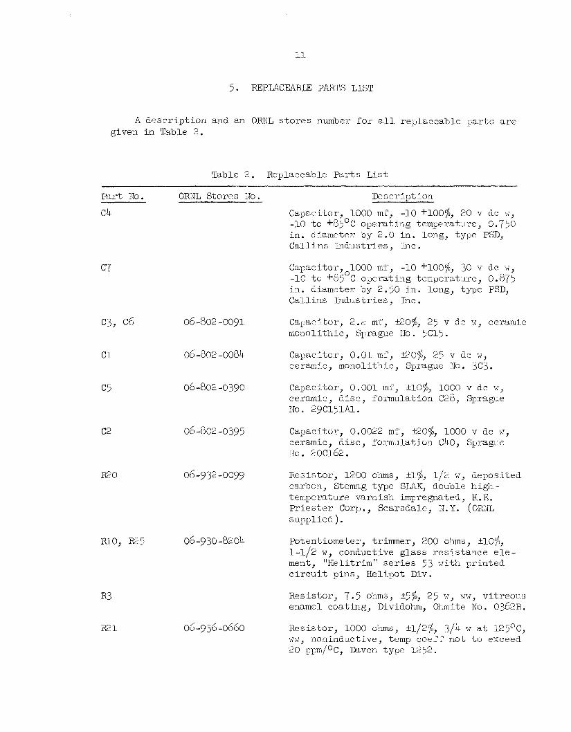
A d e s c r i p t i o n and an ORRL s t o r e s number f o r all replaceable par-ts are given i n T a b l e 2.
Table 2. Replaceable P a r t s L i s t
Part Yo. ORZL Stores 120, Des c r i p t ion
c4 Capacitor, 1000 mf, -10 +loo$, 20 v a ? v , -10 t u +8>OC ope ra t ing temperature , 0.750 i n . diameter by 2.0 i n . long, type PSD, C a l l i n s Indus t r i e s , Tnc.
c7
c2
3.320
06 -802 -0091
06 -802 -0084
06 -802 -0390
06-802 -0395
06 -932 -0099
Rlo, F j 5 06-930-8204
R 3
El 06 -936 -0660
Capacitor 1000 mi', -10 +loo$, 30 v dc -d, -10 to '85 C opera t ing temperature, 0.875 i n . diameter by 2. j0 1.n. long, type PSD, C a l l i n s Tndustries , Inc.
'0
Caijacitor., 2.d mr, e o $ , 25 v de v, ceramic monolithic, Sprague :lo. 5Cl>.
Capacitor, 0.01 m f , e o $ , 25 v de w, ce ran ic , monolithic, Sprague 110. 3C3,
Capacitor., 0.001 my, klO%, 1000 v de w, ceramic, d i s c , formulation C28, Sprague PJO . 29~151~1. Capacl-tor, 0.0022 m i , eo$ , 1000 v dc w, ceramic, d i s c , foii inilation (240, Spragie KO. 2 0 ~ 1 6 2 .
Res i s to r , 1200 ohms, ?I.$, 112 w, deposi ted carbon, Stemag type SUK, double h i@- temperature varnish impregnated, H.E. P r i e s t e r Corp., Scarsdale, TT.Y. (OXlTL suqpl ied ) . Potentiotrieter, trimmer, 200 ohms, +lo$, 1-112 w, conductive glass r e s i s t a n c e ele- ment, "He lit r i m " se s i e s 5 3 w it11 pr irzted c i r c u i t pins, Helipot Div.
Res i s to r , 7.5 ohms , +5$, 25 v, sw, vitre0u.s enamel coat ing, Dividohm, Ohrnite No. 0362B.
Res i s to r , 1000 ohms, f1/2$, 314 w a t l 2 5 O C , m~, noninductive, temp coeff n o t t o exceed 20 ppm/OC, I>izven type 1252.

I2
Tab1.e 2 (continued )
ORNL S t o r e s ?\TO. ___l_l_._
W r t :io.
Rl 1. 06-936 -0661,
H7, R9 06-936-0675
RI 2 , Rr3 ie 4
06 -9 36 -0680
R1, 1318, 06-936-068j a 2 , I130
R15 06 -936 -0692
R 1 3 06 -9 36 -069 5
R14, %8,, 06-936-0700 FQ9
k s c r i p t i o n
Res i s to r , 200 ohms, ?1/2%, 3/4 1.J ai; 1250c, iqvfir, noninductive, temp coeff not t o exceed 20 ppm/'C, a v e n type 1252.
Resistor, 400 ohms, fl/%$, 3/1h w a-t, 12j C, ww, noninductive, temp coel"f not t o exceed 20 ppm/ C, B v e n type 1252.
k s i s t o r , r(OO ohms, k1./2$, 3/14. w a t 125 C, m i , noninductive , Lernp coef f not t o exceed 20 p'prn/"~, k v e n type 12jp.
Resisto-, 1000 ohms73../2'$, 3/4 w a t lL"rj°C, w k q , noninductive, terrp c o e i f not t o exceed 20 ppm/'C, B v e n i y p 1~252.
Resis-Lor, 2000 olirtis, ?lip$, 3/4 -": a t 125 C, W W , -- I nonind-iictive, tezp coeff not, t o exceed
20 ppmj C, Daven tyye 1252*
Resiskor, 5000 ohms, ?1/2$, 3/4 i.7 a t 12j°C, - - 7 b q h , 2onindi;.ctive, temp coei? n o t t o exceed
20 ppm/ C, B v e n t y 7 e 1252-
x{esi.stor, 7000 otms, +1/2$, 3/J+ 1 1 ~ a-t 125 C , w,;;, noniridvctive, temp coef l no-t t o exceed '20 ppm/OC, Daven type 1252.
Res i s to r , 10 k l l o h m s , Ll/2$, 3/4 W at 1.5 C, :w, noninduc-Live, temp coe l f n o t t o exceed 20 ppm/ C , L v e n type 12 jSa
0
,O
0
0
.O
,O
0
0
,O
QJ, Q7 06 -996 -1585
w
Q3, Q9 06 -996 - r O 5 O
G, QV 06 -996 -199'1
D1, U6 06-555 -6244
Trans i s to r , PIT, s i l i c o n , type ~ T l l 3 l , Texas Tns 1;r . Trans i s to r , ::p?T, s i l i c o n , t y L \ e 2.l479, RCA.
Trans isioi- , PIP, type 2711084, 'i'rans i t r o n E lec t ron ic C o q .
T rans i s to r , PLY, typc DA3F3, Honey " J e l l .
Diode, s i l i c o n , type 11T1157A, g l e c t r i c a l m d - As s 0 c .

~3;bl.e ;ri (continued )
pd.X% [to. ORNL S tores DTo . Des c r i p t i.0 II
D2 06 -995 -6216 Diode, zener, 1+,'7 v, +-5$, 400 mv, type 1 P ~ 5 0 A y Motorola.
D5 Diode, zener, 9.0 v, temperatu.:ce compensated , type 1Ny39, Motorola.
In 06-995-6230 Diode, zener, 5.6 v, k5%, 400 tnv, type 1N752A, Motorola.
D10 Diode, zener, 11.7 v, temperature compen- sa ted , type 1 ~ 9 4 5 , Motorola.
F1 06 -871+ -3076 Fuse, micro, 1.5 amp, L i t t l e f u s e No. %'-(301.5.
-E 06-874-3080 Fuse, micro, 3 amp, L i t t l e f u s e Xo. 273003.
6. ACCEPTANCE TEST PROCEDURE
6.1 Test Equipment
The fol lowing t e s t equipment i s required: 1.
2. 3.
4. A temperature t e s t chamber. 5. A 33-ohm, 25-w and a lO-ohcn, 25-v r e s i s t o r f o s dumy loads.
A de regula ted po\Ter supply, adjustab1.e from 28 t o 36 v dc and
AII o sc i l l o scope , dc t o 10 MC, 1 rv/cm s e n s i t i v i t y . A d i f f e r e n t i a l - vol tmeter capable o€ r e so lv ing 10-4 v wi th inputs
capable O P supplying 2.5 amp.
from 10 t o 25 v dc.
6.2 Acceptance Test
1. Adjust t'ne power supply for 32 v dc output . Connec'i t he posit-ive terminal. of the power supply t o p i n 1-5 of t h e r egu la to r connectors, and t h e nega t ive te rmina l t o p in 10 of t'ne r e g u l a t o r connector (136).
Connect p i n 2 of' the r egu la to r t o t h e p o s i t i v e input te rmina l of t h e d i f f e r e n t i a l vol tmeter , and p in 8 of tlne r egu la to r to the nega,tive input t e rmina l of t h e vol tmeter .
2.
3. 4.
Adjust potent iometer E? u n t i l t h e voltm-eter reads 25.000 v . Connect t'ne osc i l l o scope probe t o p in 8 of t h e r egu la to r , and
connect t'ne probe ground lead t o p i n 2 of t h e r egu la to r connector. serve the osc i l l o scope t r a c e f o r any evidence o f o s c i l l a t i o n s w i t h the osc i l l o scope s e n . s i t i v i t y a t 1 r v / c m .
Ob-
14
5. Cnange i;he power supply oui;put vol'iagc: from i t s 32-v s r t t i t l g t o 28 v dc and. observe t h e osc i l l o scope tx-ace f o r evidence oi" osc i l l a t i -ons . Next, while observiiig botii t h e d t f f e r e n t i a l vol.tmeter f o r changes i n r e g u - lator output vel-tage and "ihc osc i l l o scope trac:: f o r o s c i l l a t i o n s , a d - j u s t the power su.pply vol tage slowly u n t i l . 36 v de output i s reached. 7 % ~ cha1ige j-n r e g u l a b r output volbage shoii1.d not be g r e a t e r then 2 . 5 m v from i t s value of 25.000 v. A t y p i c a l change i s less than 0.25 mv. Reset the power s i i ~ ~ - p l y output vol tage t o 32 v de.
Connec-i a 33-ohm, 2 5 4 r e s t s t o r ac ross i i in 8 and p in 2 of t h e r e g u l a t o r connector and observe the vol-tag(? change on ti1.e d i f f e r e n t i a l v o l t n e t e r . T;re vo?.tage change should no t be g r ~ x L e r -than 2.5 mv. The t y p i c a l change i s 0.25 inv. A l s o , observe t h e osci1.loscope t r a c c f o r e v i - d-ence o f o s c i l l a t i o n s while the regula-Lor i s loaded.
Connect p i n 3 of connector ~7-6 to t h e p o s i t i v e inpu t t e m i i n a l of t h e d i f f e r e n t i a l vol.tmetcr, and p i n 1% oi" conneetor PL6 t o t h e negat ive input termin21 of tile volt-meter .
6.
7.
8. 9.
Adjust potent iometer N O u n t i l t h e voltmeter reads 1.5.000 v. Connect tile osc i l l o scope probe t o p in 1.2 of connector ~16, and
connect t h e p-robe groumd k a d t o p i n 3 of connector 136. t r a c e f o r any evidence o f oscillE'Gions
10. Repeat s t e p 5 of t h e accepbance tesl;. The chmge i n t h e r e g u l a t o r output vol tage shou?.d no t b e g r e a t e r khan 1. j m v from. i t s value o f 1-5.000 v. The typical. change i s less than 0.5 mv. Reset t h e power supply vol iage t o 32 v dc. 11.
t o r ~16, and observe t h e vol tzge change on t h e differ:3ntial . voltmeter. vol tage change shou.ld not exceed 1...5 mv. Tne typica3- change i s 0.5 rnv. Ob- serve 'die o sc i l l o scope t r a c e f o r evidence of o s c i l l a t i o n s whi1.e t h e r e g u l a t o r i.s I.oruded.
12 . A temperature s t a b i l i t y t e s t c m be made by pl-ecing {;he module i n a teinperatu.re contro!.led oven. Approximately 1.5 ininu.tes should be allowzd. f o r the module t o reach equi l ibr ium a f t e r t h e oiii'ii .tiiirlperatiire i s changed.
Observe the scope on l m v / c m s e n s i t i v i t y .
Connect a lO-okm, 25-~,r r e s i s t o r ac ross ~ j h 1.2 and p i n 3 of connec- The
The -25 v vol tage regulator ciziz be t e s t e d by making t h e connections i nd ica t ed i n s'ccps 1, 2'? and 4 of t h e acceptance be;-t. 'Grace should be observed f o r evidence of o s c i l l a t i o n s during bhe -Lest,. The ou-tput voLtage of t h e -25 v dc vol.'cage regulator should not change more than 22.5 mv from i t s -25,OO v de va1iJ.e over th-e ",mpera-Lui+e range 3-0 t o 35OC. The typrical. change i s '7 mv.
%ne osc i l l o scope
The -25 v dc vol tage r e g u l a t o r can be t e s t e d by naking the connections indicated i.n s t e p s I., 7, and 9 o f the acceptsnce t e s t . Observe the o s c i l l o - scope t race f o r evri.ilixtce 0:: o s c i l l a t i o n s during t h e t e s t . The output voltage: of the -15 v dc v o l t r g e r egu la to r should not change more than 33.75 mv from i t s -1j.000 v dc vaiue over the temperature range oi" 10 t o 55'c. The t y p i c a i change i s 12 mv.

I
1.5
om-m-1638 Part 20
1-20. 21. 22. 23.
24 -33. 34-35 36-38.
39 9
40. 41 e 42. 43. 44 . 45. 46. 4'7 . J48 . 49. 50. 51.
J. L. D. s. A. E. C. J. W. D. C. T. 0. c. c . c. R. A. J. T. E. P. c. s. C. F. G. A. W. H. W . E. C. E. T. L. R. V. L. c.
Anderson Asquith G. Bztes &, rkows ki Brown Carney Cole Courtney D m d 1 Debrenzo E p l e r H a r r F 1 1 Holloway Holt Jordan Lingar M a t hews Mckan PIC Cord Cakes
INTERNAL D ISTRIBU" I O N
52. 53
54-56. 57. 58. 59 60.
61-62. 63. 64. 65.
66 -67. 68.
69-73 74 0
75; 76-90.
91..
G. R. h e n s X. W. Peelle W. Ragan J. L. Redford P. %bel J. B. Ruble G. S. Sadowski. R. W. Tucker D. D. Walker K. W. West
Central Research Library Document Eeference Sect ion Laboratory Records Department Iabora tory Zecords, 0RNL R. C. ORNL Patent Ofi'ice Division o f Technical Information
Laboratory and Univers i ty
11. N. w i m n
&tension
Division, OR0