· NUC951ADN 32-BIT ARM926EJ-S BASED MCU Publication Release Date: Sep. 10, 2012 1 Revision: A5...
590
NUC951ADN 32-BIT ARM926EJ-S BASED MCU Publication Release Date: Sep. 10, 2012 Revision: A5 1 NUC951ADN 32-bit ARM926EJ-S Based Microcontroller Product Data Sheet The information described in this document is the exclusive intellectual property of Nuvoton Technology Corporation and shall not be reproduced without permission from Nuvoton. Nuvoton is providing this document only for reference purposes of ARM926-based system design. Nuvoton assumes no responsibility for errors or omissions. All data and specifications are subject to change without notice.. For additional information or questions, please contact: Nuvoton Technology Corporation.
Transcript of · NUC951ADN 32-BIT ARM926EJ-S BASED MCU Publication Release Date: Sep. 10, 2012 1 Revision: A5...
NUC951ADN
32-BIT ARM926EJ-S BASED MCU
Publication Release Date: Sep. 10, 2012 Revision: A5 1
NUC951ADN 32-bit ARM926EJ-S Based Microcontroller
Product Data Sheet
The information described in this document is the exclusive intellectual property of Nuvoton Technology Corporation and shall not be reproduced without permission from Nuvoton.
Nuvoton is providing this document only for reference purposes of ARM926-based system design. Nuvoton assumes no responsibility for errors or omissions.
All data and specifications are subject to change without notice.. For additional information or questions, please contact: Nuvoton Technology Corporation.
NUC951ADN
32-BIT ARM926EJ-S BASED MCU
Publication Release Date: Sep. 10, 2012 Revision: A5 2
Table of Contents
1 GENERAL DESCRIPTION ......................................................................................................... 5 2 FEATURES .............................................................................................................................. 6 3 PIN DIAGRAM ...................................................................................................................... 10 4 PIN ASSIGNMENT ................................................................................................................ 11 5 PIN DESCRIPTION ............................................................................................................... 16
5.1 PIN DESCRIPTION FOR INTERFACE ............................................................................................ 16 5.2 GPIO SHARE PIN DESCRIPTION ............................................................................................... 21
6 FUNCTIONAL BLOCK ............................................................................................................ 24 7 FUNCTIONAL DESCRIPTION ................................................................................................. 25
7.1 ARM926EJ-S CPU CORE .................................................................................................... 25 7.2 SYSTEM MANAGER .............................................................................................................. 25
7.2.1 Overview ............................................................................................................... 25 7.2.2 System Memory Map ............................................................................................... 25 7.2.3 Address Bus Generation ........................................................................................... 29 7.2.4 AHB Bus Arbitration ................................................................................................ 30
7.2.4.1 Fixed Priority Mode ................................................................................................................ 30 7.2.4.2 Rotate Priority Mode .............................................................................................................. 31
7.2.5 Power-On Setting .................................................................................................... 32 7.2.6 System Booting ...................................................................................................... 33 7.2.7 System Global Control Registers Map ......................................................................... 34
7.3 CLOCK CONTROLLER ............................................................................................................ 46 7.3.1 Power management ................................................................................................ 46 7.3.2 Clock Control Registers Map ..................................................................................... 48
7.4 EXTERNAL BUS INTERFACE ..................................................................................................... 65 7.4.1 Overview ............................................................................................................... 65 7.4.2 Functional Description ............................................................................................. 65
7.4.2.1 SDRAM Controller .................................................................................................................. 65 7.4.2.2 SDRAM Components Supported ............................................................................................... 66 7.4.2.3 AHB Bus Address Mapping to SDRAM Bus .................................................................................. 67 7.4.2.4 SDRAM Power-Up Sequence .................................................................................................... 70
7.4.3 EBI Register Mapping .............................................................................................. 70 7.4.4 EBI Register Details ................................................................................................ 71
7.5 ETHERNET MAC CONTROLLER ................................................................................................. 86 EMC Descriptors ................................................................................................................... 87
7.5.1.1 Rx Buffer Descriptor ............................................................................................................... 87 7.5.1.2 Tx Buffer Descriptor ............................................................................................................... 91
7.5.2 EMC Register Mapping ............................................................................................. 96 7.5.3 EMC Register Details ............................................................................................... 98 7.5.4 Operation Notes .................................................................................................... 143
7.6 GDMA CONTROLLER ........................................................................................................... 144 7.6.1 Overview & Features .............................................................................................. 144 7.6.2 GDMA Non-Descriptor Functional Description ............................................................. 144 7.6.3 GDMA Descriptor Functional Description .................................................................... 145
7.6.3.1 Descriptor Fetch Function ..................................................................................................... 146

NUC951ADN
32-BIT ARM926EJ-S BASED MCU
Publication Release Date: Sep. 10, 2012 Revision: A5 3
7.6.3.2 Ordering function in Descriptor fetch mode .............................................................................. 148 7.6.3.3 Channel Reset ..................................................................................................................... 148 7.6.3.4 Non-Descriptor Fetch Function ............................................................................................... 149
7.6.4 GDMA Register Map ................................................................................................ 150 7.7 USB HOST CONTROLLER (USBH) ........................................................................................... 168
7.7.1 Register Mapping ................................................................................................... 169 7.7.2 Register Details ..................................................................................................... 171
7.8 USB 2.0 DEVICE CONTROLLER .............................................................................................. 217 7.8.1 USB Device Register Group Summary ....................................................................... 217 7.8.2 USB Device Control Registers Map ............................................................................ 217 7.8.3 USB Device Control Registers .................................................................................. 221
7.9 DMA CONTROLLER (DMAC) ................................................................................................. 263 7.9.1 DMA Controller Registers Map .................................................................................. 263 7.9.2 DMAC Registers ..................................................................................................... 264
7.10 FLASH MEMORY INTERFACE CONTROLLER (FMI) ........................................................................... 271 7.10.1 FMI Controller Registers Map ................................................................................... 271 7.10.2 Register Details ..................................................................................................... 273
7.11 LCD DISPLAY INTERFACE CONTROLLER (LCM) ............................................................................ 326 7.11.1 LCD Controller Function Description .......................................................................... 327
7.11.1.1 VPOST Processor .............................................................................................................. 327 7.11.1.2 Display & Overlay Control .................................................................................................. 327 7.11.1.3 Digital Display Output Control ............................................................................................ 327 7.11.1.4 Display Pin Assignment ..................................................................................................... 327
7.11.2 LCD Controller Register Map .................................................................................... 328 7.11.3 LCD Controller Register ........................................................................................... 330
7.12 AUDIO CONTROLLER ........................................................................................................... 379 7.12.1 IIS Interface ......................................................................................................... 379 7.12.2 AC97 Interface ...................................................................................................... 381 7.12.3 Audio Controller Register Map .................................................................................. 382
7.13 2-D GRAPHIC ENGINE ......................................................................................................... 411 7.13.1 2-D Graphic Engine Control Registers Map ................................................................. 411 7.13.2 2-D Graphic Engine Control Registers ....................................................................... 413
7.14 UART CONTROLLER ............................................................................................................ 441 7.14.1 UART Feature Description ........................................................................................ 441
7.14.1.1 UART0 ............................................................................................................................ 441 7.14.1.2 UART1 ............................................................................................................................ 441 7.14.1.3 UART2 ............................................................................................................................ 441
7.14.2 UART Control Registers Map .................................................................................... 442 7.15 TIMER CONTROLLER .......................................................................................................... 457
7.15.1 General Timer Controller ......................................................................................... 457 7.15.2 Watchdog Timer .................................................................................................... 457 7.15.3 Timer Control Registers Map .................................................................................... 458
7.16 ADVANCED INTERRUPT CONTROLLER ......................................................................................... 467 7.16.1 Interrupt Sources .................................................................................................. 468 7.16.2 AIC Registers Map .................................................................................................. 469
7.17 GENERAL-PURPOSE INPUT/OUTPUT (GPIO) ................................................................................ 487 7.17.1 Overview .............................................................................................................. 487 7.17.2 GPIO Multiplexed Functions Table ............................................................................. 488 7.17.3 GPIO Control Registers Map ..................................................................................... 492
7.18 REAL TIME CLOCK (RTC) ..................................................................................................... 505 7.18.1 RTC Register Mapping ............................................................................................. 505
NUC951ADN
32-BIT ARM926EJ-S BASED MCU
Publication Release Date: Sep. 10, 2012 Revision: A5 4
7.19 I2C SYNCHRONOUS SERIAL INTERFACE CONTROLLER ...................................................................... 519 7.19.1 I2C Protocol ........................................................................................................... 520 7.19.2 I2C Serial Interface Control Registers Map ................................................................. 523
7.20 UNIVERSAL SERIAL INTERFACE CONTROLLER (USI) ....................................................................... 531 7.20.1 USI Timing Diagram ............................................................................................... 532 7.20.2 USI Control Registers Map ....................................................................................... 533
7.21 PULSE WIDTH MODULATION (PWM) ........................................................................................ 543 7.21.1 Basic Timer Operation ............................................................................................ 544 7.21.2 PWM Double Buffering and Reload Automatically ........................................................ 544 7.21.3 Modulate Duty Ratio ............................................................................................... 546 7.21.4 Dead Zone Generator ............................................................................................. 546 7.21.5 PWM Timer Start Procedure ..................................................................................... 547 7.21.6 PWM Timer Stop Procedure ..................................................................................... 547 7.21.7 PWM Register Map ................................................................................................. 547
7.22 KEYPAD INTERFACE (KPI) .................................................................................................... 557 7.22.1 Keypad Interface Register Map ................................................................................ 558 7.22.2 Timing Diagram ..................................................................................................... 563
7.23 PS2 HOST INTERFACE CONTROLLER ......................................................................................... 564 7.23.1 PS2 Host Controller Interface Register Map ................................................................ 564
8 ELECTRICAL SPECIFICATIONS ........................................................................................... 571 8.1 ABSOLUTE MAXIMUM RATINGS ............................................................................................... 571 8.2 DC SPECIFICATIONS ........................................................................................................... 572
8.2.1 Digital DC Characteristics ........................................................................................ 572 8.2.2 USB Low-/Full-Speed DC Electrical Specifications ........................................................ 573 8.2.3 USB High-Speed DC Electrical Specifications .............................................................. 573
8.3 AC SPECIFICATIONS ........................................................................................................... 574 8.3.1 RESET AC Characteristics ........................................................................................ 574 8.3.2 Clock Input Characteristics ...................................................................................... 574 8.3.3 EBI/SDRAM Interface AC Characteristics ................................................................... 575 8.3.4 EBI(ROM/SRAM/External I/O) AC Characteristics ........................................................ 576 8.3.5 External DMA nXDREQ/nXDACK AC Characteristics ..................................................... 577 8.3.6 LCD Interface: MPU Type AC Characteristics .............................................................. 578 8.3.7 SD Host Interface AC Characteristics ........................................................................ 579 8.3.8 NAND Flash Memory Interface AC Characteristics ....................................................... 580 8.3.9 Memory Stick Interface AC Characteristics ................................................................. 581 8.3.10 Audio AC-Link Interface AC Characteristics ................................................................ 582 8.3.11 Audio I2S Interface AC Characteristics ...................................................................... 583 8.3.12 USI(SPI/MW) Interface AC Characteristics ................................................................. 584 8.3.13 USB Transceiver AC Characteristics .......................................................................... 585 8.3.14 EMC RMII AC Characteristics ................................................................................... 586
9 PACKAGE SPECIFICATIONS ................................................................................................ 588 10 REVISION HISTORY ........................................................................................................ 589
NUC951ADN
32-BIT ARM926EJ-S BASED MCU
Publication Release Date: Sep. 10, 2012 Revision: A5 5
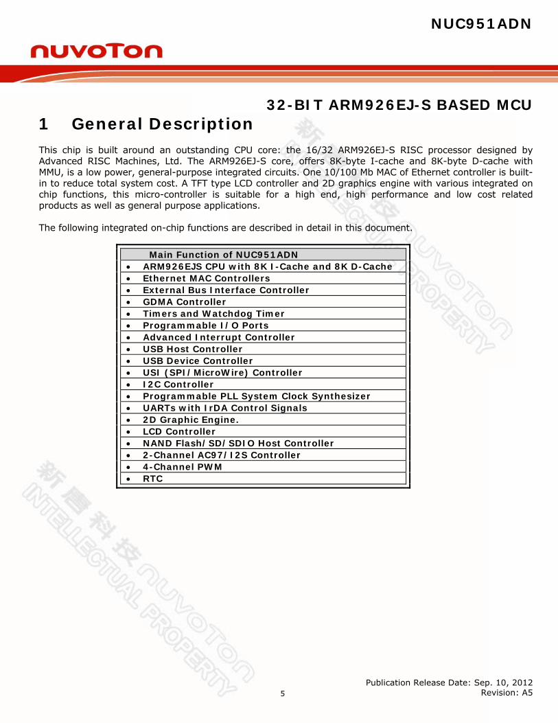
1 General Description This chip is built around an outstanding CPU core: the 16/32 ARM926EJ-S RISC processor designed by Advanced RISC Machines, Ltd. The ARM926EJ-S core, offers 8K-byte I-cache and 8K-byte D-cache with MMU, is a low power, general-purpose integrated circuits. One 10/100 Mb MAC of Ethernet controller is built-in to reduce total system cost. A TFT type LCD controller and 2D graphics engine with various integrated on chip functions, this micro-controller is suitable for a high end, high performance and low cost related products as well as general purpose applications. The following integrated on-chip functions are described in detail in this document.
Main Function of NUC951ADN ARM926EJS CPU with 8K I-Cache and 8K D-Cache Ethernet MAC Controllers External Bus Interface Controller GDMA Controller Timers and Watchdog Timer Programmable I/O Ports Advanced Interrupt Controller USB Host Controller USB Device Controller USI (SPI/MicroWire) Controller I2C Controller Programmable PLL System Clock Synthesizer UARTs with IrDA Control Signals 2D Graphic Engine. LCD Controller NAND Flash/SD/SDIO Host Controller 2-Channel AC97/I2S Controller 4-Channel PWM RTC
NUC951ADN
32-BIT ARM926EJ-S BASED MCU
Publication Release Date: Sep. 10, 2012 Revision: A5 6
2 Features Architecture Efficient and powerful ARM926EJS core with fully 16/32-bit RISC architecture Little Endian mode supported 8K-byte I-cache and 8K-byte D-cache with MMU Cost-effective JTAG-based debug solution External Bus Interface 8/16/32-bit external bus support for ROM/SRAM, flash memory, SDRAM and external I/Os Supports up to 3 chip select (nECS[0], nECS[1] and nECS[3]) pins. Supports external DMA request/acknowledge for external device connecting on external I/O bank 3
(nECS[3]). Programmable access cycle (0-7 wait cycle) Four-word depth write buffer Ethernet MAC Controller 100/10-Mbps operation DMA engine with burst mode MAC Tx/Rx buffers (256 bytes Tx, 256 bytes Rx) Full compliance with IEEE standard 802.3 RMII interface only Station Management Signaling On-Chip CAM (up to 16 destination addresses) Full-duplex mode with PAUSE feature Long/short packet modes LCD Controller Support the 8/12/16/18-bit data interface to connect with 80/68 series MPU type LCM module Convert RGB-565, YUV-422 display data to RGB-444, RGB-565, RGB-666, YUV-422 color format for
display output Support CCIR-656( with vsync / hsync / data enable sync signal ) 8/16-bit YUV data output format to
connect with external TV encoder Support 8/16 bpp OSD data with video overlay function to facilitate the diverse graphic UI. Support linear 1X – 8X image scaling up function. Support Picture-In-Picture display function Support hardware cursor.
General DMA Controller 2-channel General DMA for memory-to-memory data transfers without CPU intervention Support 1 external DMA request for external device connecting to EBI external I/O bank 3 (nECS[3]). Increments or decrements a source or destination address in 8-bit, 16-bit or 32-bit data transfers 4-data burst mode

NUC951ADN
32-BIT ARM926EJ-S BASED MCU
Publication Release Date: Sep. 10, 2012 Revision: A5 7
UART Three UART (serial I/O) blocks with interrupt-based operation Support for 5-bit, 6-bit, 7-bit or 8-bit serial data transmit and receive Programmable baud rates 1,1½ or 2 stop bits Odd or even parity Break generation and detection Parity, overrun and framing error detection X16 clock mode Support for IrDA and two debug ports Timers Five programmable 24-bit timers with 8-bit pre-scalar One programmable 20-bit Watchdog timer One-short mode, period mode or toggle mode operation Programmable I/Os Pins individually configurable to input, output or I/O mode for dedicated signals I/O ports are Programmable and Configurable for Multiple functions Advanced Interrupt Controller 31 interrupt sources, including 3 external interrupt sources Programmable normal or fast interrupt mode (IRQ, FIQ) Programmable as either edge-triggered or level-sensitive for 3 external interrupt sources Programmable as either low-active or high-active for 3 external interrupt sources Priority methodology is encoded to allow for interrupt daisy-chaining Automatically mask out the lower priority interrupt during interrupt nesting Automatically clear the interrupt flag when the interrupt source is programmed to be edge-triggered USB Host Controller with tranceiver Fully compliant with USB Revision 2.0 specification. Enhanced Host Controller Interface (EHCI) Revision 1.0 compatible. Open Host Controller Interface (OHCI) Revision 1.0 compatible. Supports high-speed (480Mbps), full-speed (12Mbps) and low-speed (1.5Mbps) USB devices. Supports Control, Bulk, Interrupt, Isochronous and Split transfers. Built-in DMA for real-time data transfer. Support two ports (one port transceiver is shared with USB Device Controller)
USB Device Controller with tranceiver Compliant with USB version 2.0 specification. Software control for device remote-wakeup. Supports 6 configurable IN/OUT endpoints in addition to Control Endpoint. Each of these endpoints can
be configures as In or Out with Isochronous, Bulk or Interrupt transfer. Three different modes of operation of an in-endpoint (Auto validation mode, manual validation mode,
Fly mode. Supports Endpoint Maximum Packet Size up to 1024 bytes.
NUC951ADN
32-BIT ARM926EJ-S BASED MCU
Publication Release Date: Sep. 10, 2012 Revision: A5 8
PLL Supports two on-chip PLLs The external clock can be multiplied by on-chip PLL to provide high frequency system clock The input frequency range is 4-30MHz; 15MHz is preferred. Programmable clock frequency 4-Channel PWM Four 16-bit timers Two 8-bit pre-scalars & Two 4-bit divider Programmable duty control of output waveform (PWM) Auto reload mode or one-shot pulse mode Dead-zone generator I2C Master support master mode only Multi Master Operation Clock stretching and wait state generation Provide multi-byte transmit operation, up to 4 bytes can be transmitted in a single transfer Software programmable acknowledge bit Arbitration lost interrupt, with automatic transfer cancellation Start/Stop/Repeated Start/Acknowledge generation Start/Stop/Repeated Start detection Bus busy detection Supports 7 bit addressing mode Software mode I2C Universal Serial Interface (USI) Support MICROWIRE/SPI master mode Support full/half duplex synchronous serial data transfer Variable length of transfer word up to 32 bits Provide burst mode operation, transmit/receive can be executed up to four times in one transfer MSB or LSB first data transfer Receive and Transmit on both rising or falling edge of serial clock independently
2-Channel AC97/I2S Controller Always 8-beat incrementing burst Always bus lock when 8-beat incrementing burst Flash Memory Interface (FMI) Directly connect to Secure Digital (SD, MMC and SDIO) flash memory card, Memory Stick (Memory
stick PRO) and NAND type flash memory. Supports DMA function to accelerate the data transfer between the internal buffer, external SDRAM,
and flash memory card. Two 512 bytes internal buffers are embedded inside PS2 Host Interface IBM PS2 or AT-compatible keyboard or mouse interface Half-Duplex Bi-directional synchronous serial interface using op-drain outputs for clock and data
NUC951ADN
32-BIT ARM926EJ-S BASED MCU
Publication Release Date: Sep. 10, 2012 Revision: A5 9
Odd parity generation and checking Real Time Clock (RTC) Time counter (second, minute, hour) and calendar counter (day, month, year) Alarm register (second, minute, hour, day, month, year) 12 or 24-hour mode selectable Recognize leap year automatically Day of the week counter Frequency compensate register (FCR) Beside FCR, all clock and alarm data expressed in BCD code Support tick time interrupt 2-D Graphics Engine Color depth 8-bit/16-bit/32-bit in RGB domain or RGB332/RGB565/RGB888 are supported Contains 2D Bit Block Transfer (BitBLT) functions as defined in Microsoft GDI. It includes HostBLT,
Pattern BLT, Color/Font Expanding BLT, Transparent BLT, Tile BLT, BlockMove BLT, CopyFile BLT, Color/Font Expansion, and Rectangle Fill, etc.
Supports fore/background colors and all Microsoft 256 ternary raster-operation codes (ROP) Clipping window can be defined as inside or outside clipping Implements the alpha-blending function for source/destination picture overlaying Fast Bresenham line drawing algorithm is used to draw solid/textured lines Supports rectangular border or frame drawing Supports picture re-sizing by 1/255 ~ 254/255 down-scaling and 1 ~ 1.996 up-scaling (1+254/255). Supports object rotations in different degrees, that is L45/L90/R45/R90/M180/F180/X180, where
L45/L90 means rotate left 45/90 degrees, R45/R90 means rotate right 45/90 degrees, M180 means mirror (flop), F180 means up-side-down(flip), and X180 for rotations by 180 degrees
Power management Programmable clock enable for individual peripherals IDLE mode to halt ARM Core and keep peripheral working Power-Down mode to stop all clocks included external crystal oscillator. Exit IDLE/Power-Down by interrupts Operation Voltage Range 3.3 V for IO Buffer 1.8 V for Core Logic Operation Temperature Range -40~+85 Operating Frequency Up to 200 MHz for ARM926EJS CPU Package Type 216-Pin LQFP
NUC951ADN
32-BIT ARM926EJ-S BASED MCU
Publication Release Date: Sep. 10, 2012 Revision: A5 10
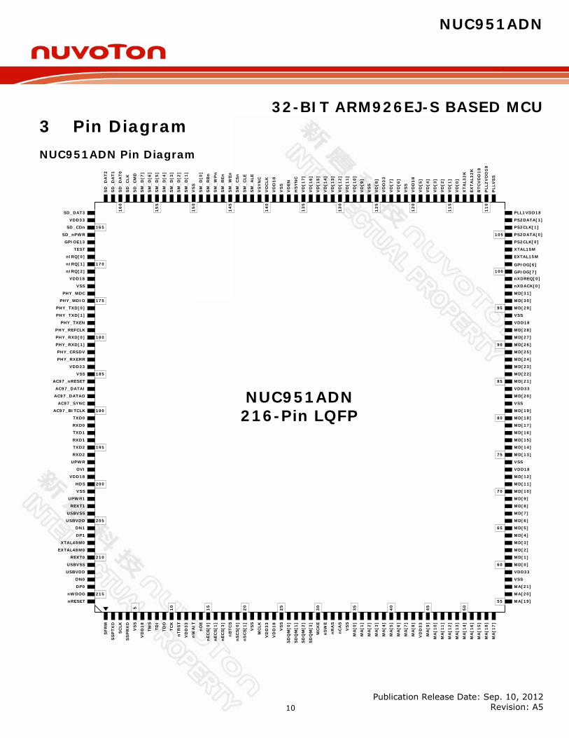
3 Pin Diagram NUC951ADN Pin Diagram
5
NUC951ADN216-Pin LQFP
10
15
20
25
30
80
85
90
95
100
11
0
11
5
12
0
165
170
180
190
195
nRESET
SS
PTX
D
SC
LK
SS
PR
XD
VS
S
VD
D1
8
nO
E
nB
TC
S
nS
CS
[0]
VS
S
MC
LK
SD
QM
[0]
SD
QM
[1]
nS
WE
nR
AS
nC
AS
MA
[0]
MA
[1]
MA
[2]
MA
[3]
MA
[4]
MA
[5]
MA
[6]
MA
[7]
MA
[8]
MA
[9]
MA
[10
]
MA
[12
]
MD[11]
MD[12]
MD[13]
MD[14]
MD[15]
PS2CLK[0]
PS2DATA[0]
EXTAL15M
XTAL15M
VD
[14
]
VD
[15
]
VD
[16
]
VD
[17
]
VS
S
HS
YN
C
VD
EN
VD
D1
8
VO
CLK
VS
YN
C
SM
_A
LE
SM
_C
LE
SM
_C
Sn
SM
_W
En
SM
_R
En
SM
_W
Pn
SM
_R
Bn
SM
_D
[0]
VS
S
SM
_D
[1]
SM
_D
[2]
SM
_D
[3]
SM
_D
[4]
SM
_D
[5]
SM
_D
[6]
SM
_D
[7]
SD
_C
MD
SD
_C
LK
SD
_D
AT
0
SD
_D
AT
1
SD_DAT3
SD_nPWR
GPIOE13
TEST
nIRQ[0]
nIRQ[1]
nIRQ[2]
VDD18
VSS
PHY_MDC
PHY_MDIO
PHY_CRSDV
PHY_RXD[0]
PHY_TXEN
PHY_REFCLK
PHY_TXD[0]
PHY_TXD[1]
PHY_RXD[1]
VSS
TXD0
AC97_DATAO
AC97_SYNC
RXD0
AC97_BITCLK
TXD1
AC97_nRESET
AC97_DATAI
VDD33
PHY_RXERR
MC
KE
nE
CS
[0]
SD
_D
AT
2
VDD33
SD_CDn
MA[20]
MA[21]
VSS
VDD33
VSS
MD[0]
MD[1]
MD[2]
MD[3]
MD[4]
MD[5]
MD[6]
MD[7]
MD[8]
MD[9]
MA[19]
PLL
VS
S
PLL
2V
DD
18
RTC
VD
D1
8
EX
TAL3
2K
VD
[1]
XT
AL3
2K
VD
[0]
VD
[2]
VD
[3]
VD
[4]
VD
[5]
VD
D1
8
VS
S
VD
[6]
VD
[7]
VD
D3
3
VD
[8]
VS
S
VD
[9]
VD
[10
]
VD
[11
]
VD
[12
]
VD
[13
]
RXD1
TXD2
RXD2
UPWR
USBVSS
UPWR1
HDS
VSS
OVI
VDD18
REXT1
DP1
USBVSS
XTAL48M0
EXTAL48M0
USBVDD
REXT0
DN0
DN1
USBVDD
DP0
SFR
M
TMS
TDI
TD
O
TCK
nTR
ST
VD
D3
3
nW
AIT
nE
CS
[1]
nE
CS
[3]
nS
CS
[1]
VD
D3
3
VD
D1
8
VS
S
SD
QM
[2]
SD
QM
[3]
VS
S
35
40
VD
D3
3
MA
[11
]
45
MA
[14
]
MA
[13
]
50
MA
[16
]
MA
[15
]
MA
[18
]
MA
[17
]
55
60
65
MD[10]70
VDD18
75
MD[16]
MD[17]
MD[18]
MD[19]
VSS
MD[20]
VDD33
MD[21]
MD[22]
MD[23]
MD[24]
MD[25]
MD[26]
MD[27]
MD[28]
VDD18
VSS
MD[29]
MD[30]
MD[31]
nXDACK[0]
nXDREQ[0]GPIOG[7]
GPIOG[6]
PS2CLK[1]
PS2DATA[1]
PLL1VDD18
105
12
5
13
0
13
5
14
0
14
5
15
0
15
5
16
0
175
185
200
205
210
215nWDOG
NUC951ADN
32-BIT ARM926EJ-S BASED MCU
Publication Release Date: Sep. 10, 2012 Revision: A5 11
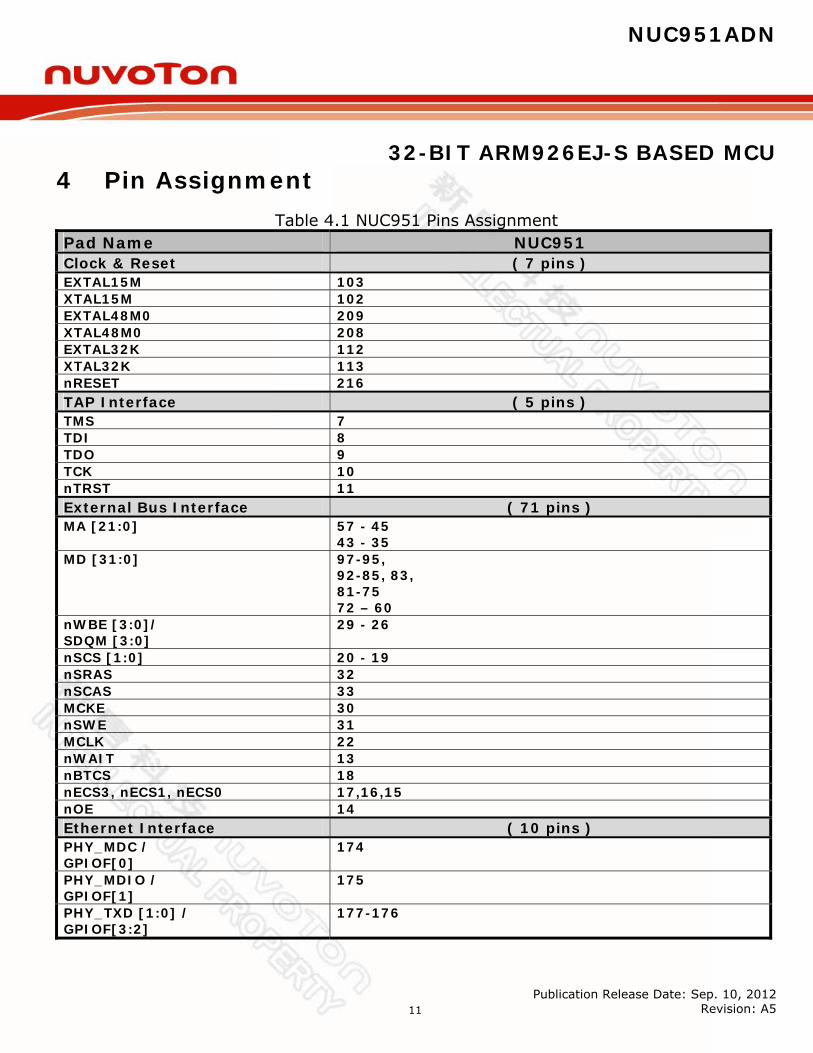
4 Pin Assignment
Table 4.1 NUC951 Pins Assignment
Pad Name NUC951 Clock & Reset ( 7 pins ) EXTAL15M 103 XTAL15M 102 EXTAL48M0 209 XTAL48M0 208 EXTAL32K 112 XTAL32K 113 nRESET 216 TAP Interface ( 5 pins ) TMS 7 TDI 8 TDO 9 TCK 10 nTRST 11 External Bus Interface ( 71 pins ) MA [21:0] 57 - 45
43 - 35 MD [31:0] 97-95,
92-85, 83, 81-75 72 – 60
nWBE [3:0]/ SDQM [3:0]
29 - 26
nSCS [1:0] 20 - 19 nSRAS 32 nSCAS 33 MCKE 30 nSWE 31 MCLK 22 nWAIT 13 nBTCS 18 nECS3, nECS1, nECS0 17,16,15 nOE 14 Ethernet Interface ( 10 pins ) PHY_MDC / GPIOF[0]
174
PHY_MDIO / GPIOF[1]
175
PHY_TXD [1:0] / GPIOF[3:2]
177-176

NUC951ADN
32-BIT ARM926EJ-S BASED MCU
Publication Release Date: Sep. 10, 2012 Revision: A5 12
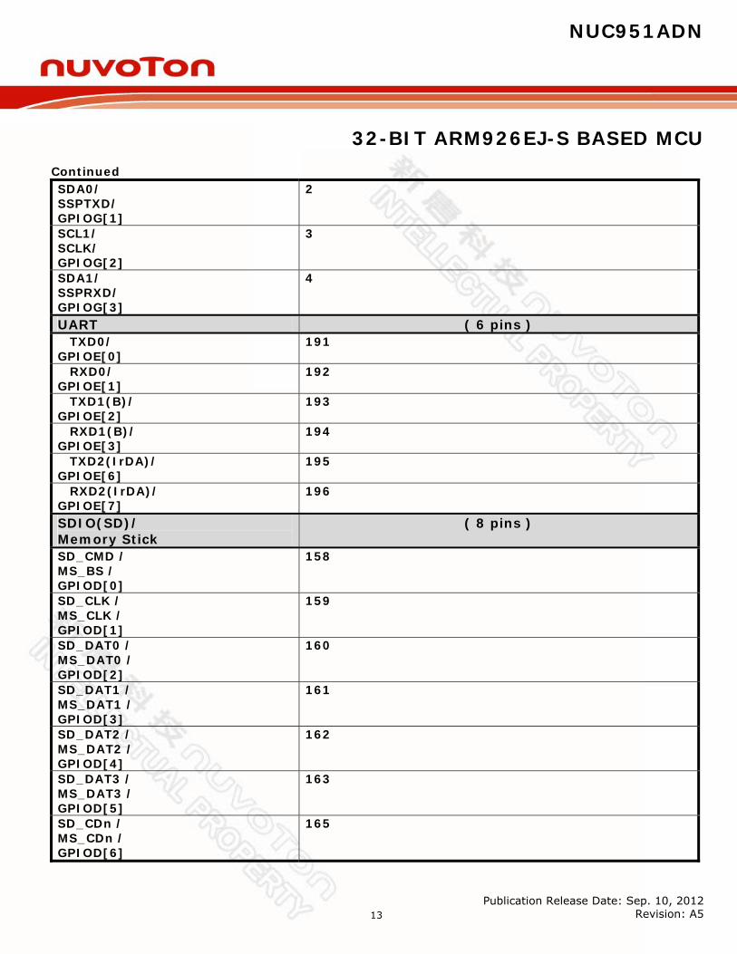
Continued PHY_TXEN/ GPIOF[4]
178
PHY_REFCLK/ GPIOF[5]
179
PHY_RXD [1:0]/ GPIOF[7:6]
181-180
PHY_CRSDV/ GPIOF[8]
182
PHY_RXERR/ GPIOF[9]
183
AC97/I2S/PWM ( 5 pins ) AC97_nRESET/ I2S_SYSCLK/ GPIOG[12]
186
AC97_DATAI/ I2S_DATAI/ PWM [0] / GPIOG[13]
187
AC97_DATAO/ I2S_DATAO/ PWM[1]/ GPIOG[14]
188
AC97_SYNC/ I2S_WS/ PWM[2]/ GPIOG[15]
189
AC97_BITCLK/ I2S_BITCLK/ PWM[3]/ GPIOG[16]
190
USB Interface ( 10 pins ) DP0 214 DN0 213 REXT0 210 UPWR0 197 OVI 198 HDS 200 DP1 207 DN1 206 REXT1 203 UPWR1 202 I2C/USI(SPI/MW) ( 4 pins ) SCL0/ SFRM/ GPIOG[0]
1
NUC951ADN
32-BIT ARM926EJ-S BASED MCU
Publication Release Date: Sep. 10, 2012 Revision: A5 13
Continued SDA0/ SSPTXD/ GPIOG[1]
2
SCL1/ SCLK/ GPIOG[2]
3
SDA1/ SSPRXD/ GPIOG[3]
4
UART ( 6 pins ) TXD0/
GPIOE[0] 191
RXD0/ GPIOE[1]
192
TXD1(B)/ GPIOE[2]
193
RXD1(B)/ GPIOE[3]
194
TXD2(IrDA)/ GPIOE[6]
195
RXD2(IrDA)/ GPIOE[7]
196
SDIO(SD)/ Memory Stick
( 8 pins )
SD_CMD / MS_BS / GPIOD[0]
158
SD_CLK / MS_CLK / GPIOD[1]
159
SD_DAT0 / MS_DAT0 / GPIOD[2]
160
SD_DAT1 / MS_DAT1 / GPIOD[3]
161
SD_DAT2 / MS_DAT2 / GPIOD[4]
162
SD_DAT3 / MS_DAT3 / GPIOD[5]
163
SD_CDn / MS_CDn / GPIOD[6]
165
NUC951ADN
32-BIT ARM926EJ-S BASED MCU
Publication Release Date: Sep. 10, 2012 Revision: A5 14
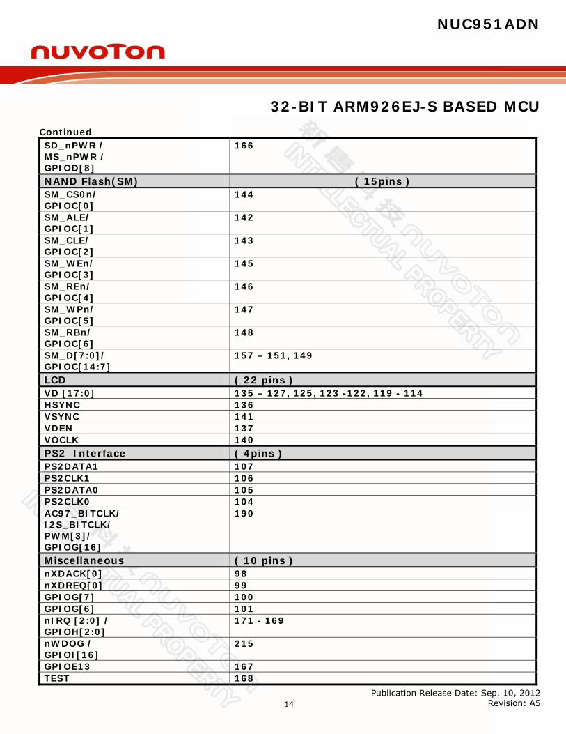
Continued SD_nPWR / MS_nPWR / GPIOD[8]
166
NAND Flash(SM) ( 15pins ) SM_CS0n/ GPIOC[0]
144
SM_ALE/ GPIOC[1]
142
SM_CLE/ GPIOC[2]
143
SM_WEn/ GPIOC[3]
145
SM_REn/ GPIOC[4]
146
SM_WPn/ GPIOC[5]
147
SM_RBn/ GPIOC[6]
148
SM_D[7:0]/ GPIOC[14:7]
157 – 151, 149
LCD ( 22 pins ) VD [17:0] 135 – 127, 125, 123 -122, 119 - 114 HSYNC 136 VSYNC 141 VDEN 137 VOCLK 140 PS2 Interface ( 4pins ) PS2DATA1 107 PS2CLK1 106 PS2DATA0 105 PS2CLK0 104 AC97_BITCLK/ I2S_BITCLK/ PWM[3]/ GPIOG[16]
190
Miscellaneous ( 10 pins ) nXDACK[0] 98 nXDREQ[0] 99 GPIOG[7] 100 GPIOG[6] 101 nIRQ [2:0] / GPIOH[2:0]
171 - 169
nWDOG / GPIOI[16]
215
GPIOE13 167 TEST 168

NUC951ADN
32-BIT ARM926EJ-S BASED MCU
Publication Release Date: Sep. 10, 2012 Revision: A5 15
Continued
Power/Ground (39 pins) VDD18 6, 24, 73, 93, 120, 139, 172, 199 VDD33 12, 23, 44, 59, 84, 124, 164, 184 VSS 5, 21, 25, 34, 58, 74, 82, 94,121, 126, 138, 150,173,
185, 201 USBVSS 204, 211 USBVDD (3.3V) 205, 212 PLLVDD (1.8V) 108, 110 PLLVSS 109 RTCVDD (1.8V) 111
NUC951ADN
32-BIT ARM926EJ-S BASED MCU
Publication Release Date: Sep. 10, 2012 Revision: A5 16
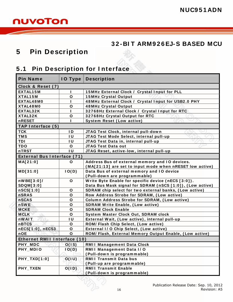
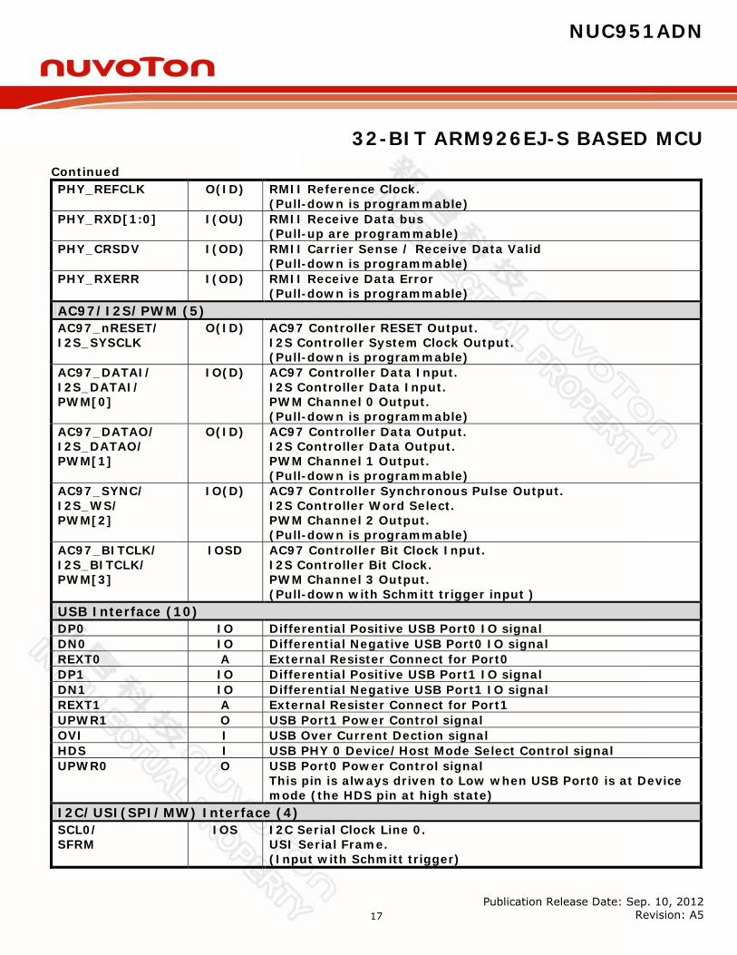
5 Pin Description
5.1 Pin Description for Interface Pin Name IO Type Description Clock & Reset (7) EXTAL15M I 15MHz External Clock / Crystal Input for PLL XTAL15M O 15MHz Crystal Output EXTAL48M0 I 48MHz External Clock / Crystal Input for USB2.0 PHY XTAL48M0 O 48MHz Crystal Output EXTAL32K I 32768Hz External Clock / Crystal Input for RTC XTAL32K O 32768Hz Crystal Output for RTC nRESET I System Reset (Low active) TAP Interface (5) TCK ID JTAG Test Clock, internal pull-down TMS IU JTAG Test Mode Select, internal pull-up TDI IU JTAG Test Data in, internal pull-up TDO O JTAG Test Data out nTRST IU JTAG Reset, active-low, internal pull-up External Bus Interface (71) MA[21:0] O Address Bus of external memory and IO devices.
(MA[21:13] are set to input mode when nRESET low active) MD[31:0] IO(D) Data Bus of external memory and IO device
(Pull-down are programmable) nWBE[3:0]/ SDQM[3:0]
O Write Byte Enable for specific device (nECS [3:0]). Data Bus Mask signal for SDRAM (nSCS [1:0]), (Low active)
nSCS[1:0] O SDRAM chip select for two external banks, (Low active) nSRAS O Row Address Strobe for SDRAM, (Low active) nSCAS O Column Address Strobe for SDRAM, (Low active) nSWE O SDRAM Write Enable, (Low active) MCKE O SDRAM Clock Enable MCLK O System Master Clock Out, SDRAM clock nWAIT IU External Wait, (Low active), internal pull-up nBTCS O ROM/Flash Chip Select, (Low active) nECS[1:0], nECS3 O External I/O Chip Select, (Low active) nOE O ROM/Flash, External Memory Output Enable, (Low active) Ethernet RMII Interface (10) PHY_MDC O(IS) RMII Management Data Clock PHY_MDIO IO(D) RMII Management Data I/O
(Pull-down is programmable) PHY_TXD[1:0] O(IU) RMII Transmit Data bus
(Pull-up are programmable) PHY_TXEN O(ID) RMII Transmit Enable
(Pull-down is programmable)
NUC951ADN
32-BIT ARM926EJ-S BASED MCU
Publication Release Date: Sep. 10, 2012 Revision: A5 17
Continued PHY_REFCLK O(ID) RMII Reference Clock.
(Pull-down is programmable) PHY_RXD[1:0] I(OU) RMII Receive Data bus
(Pull-up are programmable) PHY_CRSDV I(OD) RMII Carrier Sense / Receive Data Valid
(Pull-down is programmable) PHY_RXERR I(OD) RMII Receive Data Error
(Pull-down is programmable) AC97/I2S/PWM (5) AC97_nRESET/ I2S_SYSCLK
O(ID) AC97 Controller RESET Output. I2S Controller System Clock Output. (Pull-down is programmable)
AC97_DATAI/ I2S_DATAI/ PWM[0]
IO(D) AC97 Controller Data Input. I2S Controller Data Input. PWM Channel 0 Output. (Pull-down is programmable)
AC97_DATAO/ I2S_DATAO/ PWM[1]
O(ID) AC97 Controller Data Output. I2S Controller Data Output. PWM Channel 1 Output. (Pull-down is programmable)
AC97_SYNC/ I2S_WS/ PWM[2]
IO(D) AC97 Controller Synchronous Pulse Output. I2S Controller Word Select. PWM Channel 2 Output. (Pull-down is programmable)
AC97_BITCLK/ I2S_BITCLK/ PWM[3]
IOSD AC97 Controller Bit Clock Input. I2S Controller Bit Clock. PWM Channel 3 Output. (Pull-down with Schmitt trigger input )
USB Interface (10) DP0 IO Differential Positive USB Port0 IO signal DN0 IO Differential Negative USB Port0 IO signal REXT0 A External Resister Connect for Port0 DP1 IO Differential Positive USB Port1 IO signal DN1 IO Differential Negative USB Port1 IO signal REXT1 A External Resister Connect for Port1 UPWR1 O USB Port1 Power Control signal OVI I USB Over Current Dection signal HDS I USB PHY 0 Device/Host Mode Select Control signal UPWR0 O USB Port0 Power Control signal
This pin is always driven to Low when USB Port0 is at Device mode (the HDS pin at high state)
I2C/USI(SPI/MW) Interface (4) SCL0/ SFRM
IOS I2C Serial Clock Line 0. USI Serial Frame. (Input with Schmitt trigger)
NUC951ADN
32-BIT ARM926EJ-S BASED MCU
Publication Release Date: Sep. 10, 2012 Revision: A5 18
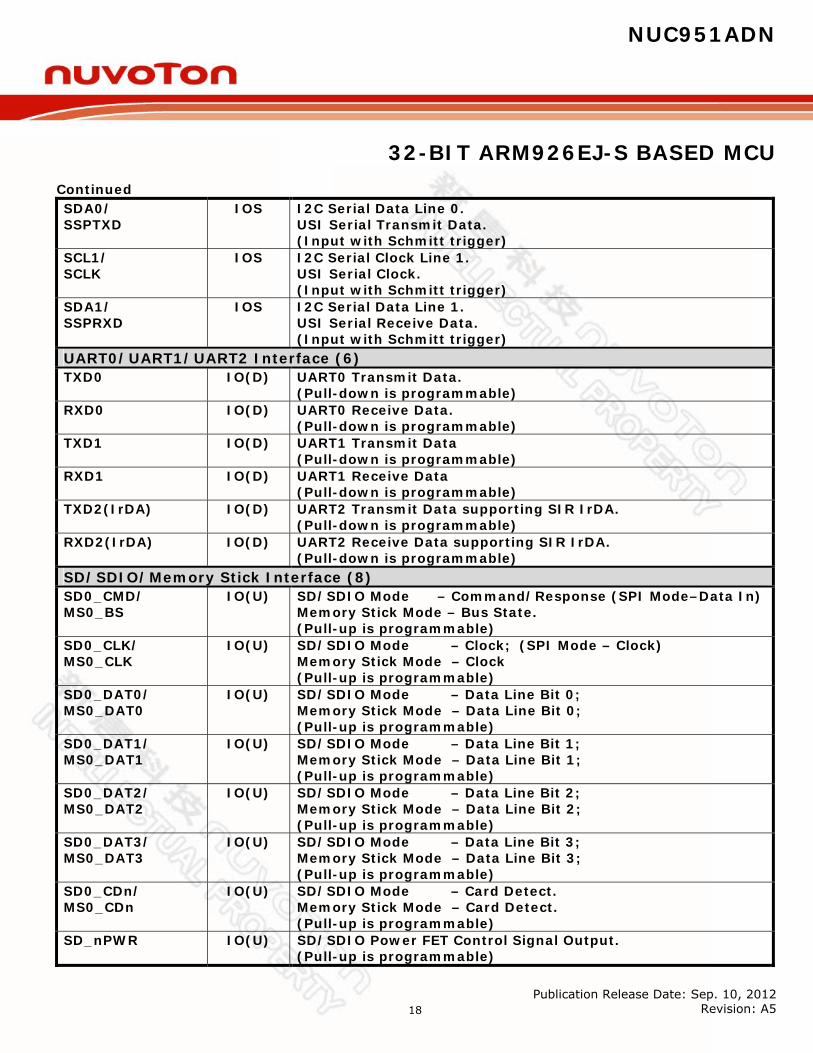
Continued SDA0/ SSPTXD
IOS I2C Serial Data Line 0. USI Serial Transmit Data. (Input with Schmitt trigger)
SCL1/ SCLK
IOS I2C Serial Clock Line 1. USI Serial Clock. (Input with Schmitt trigger)
SDA1/ SSPRXD
IOS I2C Serial Data Line 1. USI Serial Receive Data. (Input with Schmitt trigger)
UART0/UART1/UART2 Interface (6) TXD0 IO(D) UART0 Transmit Data.
(Pull-down is programmable) RXD0 IO(D) UART0 Receive Data.
(Pull-down is programmable) TXD1 IO(D) UART1 Transmit Data
(Pull-down is programmable) RXD1 IO(D) UART1 Receive Data
(Pull-down is programmable) TXD2(IrDA) IO(D) UART2 Transmit Data supporting SIR IrDA.
(Pull-down is programmable) RXD2(IrDA) IO(D) UART2 Receive Data supporting SIR IrDA.
(Pull-down is programmable) SD/SDIO/Memory Stick Interface (8) SD0_CMD/ MS0_BS
IO(U) SD/SDIO Mode – Command/Response (SPI Mode–Data In) Memory Stick Mode – Bus State. (Pull-up is programmable)
SD0_CLK/ MS0_CLK
IO(U) SD/SDIO Mode – Clock; (SPI Mode – Clock) Memory Stick Mode – Clock (Pull-up is programmable)
SD0_DAT0/ MS0_DAT0
IO(U) SD/SDIO Mode – Data Line Bit 0; Memory Stick Mode – Data Line Bit 0; (Pull-up is programmable)
SD0_DAT1/ MS0_DAT1
IO(U) SD/SDIO Mode – Data Line Bit 1; Memory Stick Mode – Data Line Bit 1; (Pull-up is programmable)
SD0_DAT2/ MS0_DAT2
IO(U) SD/SDIO Mode – Data Line Bit 2; Memory Stick Mode – Data Line Bit 2; (Pull-up is programmable)
SD0_DAT3/ MS0_DAT3
IO(U) SD/SDIO Mode – Data Line Bit 3; Memory Stick Mode – Data Line Bit 3; (Pull-up is programmable)
SD0_CDn/ MS0_CDn
IO(U) SD/SDIO Mode – Card Detect. Memory Stick Mode – Card Detect. (Pull-up is programmable)
SD_nPWR IO(U) SD/SDIO Power FET Control Signal Output. (Pull-up is programmable)
NUC951ADN
32-BIT ARM926EJ-S BASED MCU
Publication Release Date: Sep. 10, 2012 Revision: A5 19
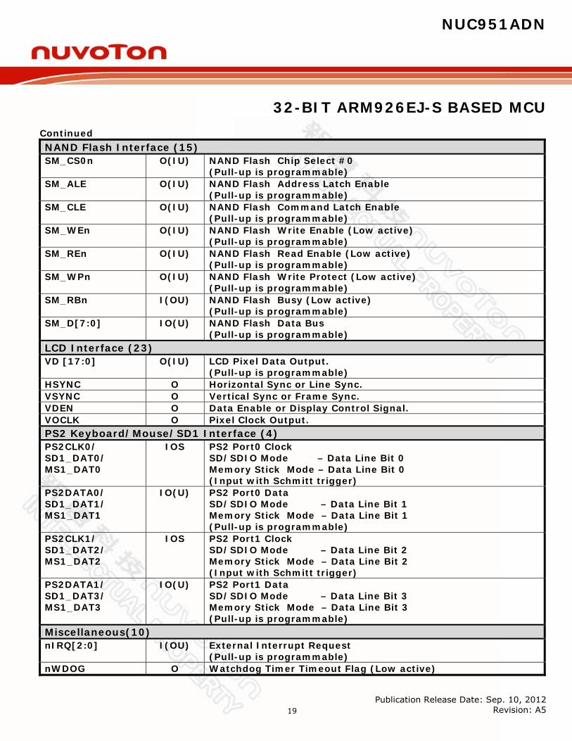
Continued NAND Flash Interface (15) SM_CS0n O(IU) NAND Flash Chip Select #0
(Pull-up is programmable) SM_ALE O(IU) NAND Flash Address Latch Enable
(Pull-up is programmable) SM_CLE O(IU) NAND Flash Command Latch Enable
(Pull-up is programmable) SM_WEn O(IU) NAND Flash Write Enable (Low active)
(Pull-up is programmable) SM_REn O(IU) NAND Flash Read Enable (Low active)
(Pull-up is programmable) SM_WPn O(IU) NAND Flash Write Protect (Low active)
(Pull-up is programmable) SM_RBn I(OU) NAND Flash Busy (Low active)
(Pull-up is programmable) SM_D[7:0] IO(U) NAND Flash Data Bus
(Pull-up is programmable) LCD Interface (23) VD [17:0] O(IU) LCD Pixel Data Output.
(Pull-up is programmable) HSYNC O Horizontal Sync or Line Sync. VSYNC O Vertical Sync or Frame Sync. VDEN O Data Enable or Display Control Signal. VOCLK O Pixel Clock Output. PS2 Keyboard/Mouse/SD1 Interface (4) PS2CLK0/ SD1_DAT0/ MS1_DAT0
IOS PS2 Port0 Clock SD/SDIO Mode – Data Line Bit 0 Memory Stick Mode – Data Line Bit 0 (Input with Schmitt trigger)
PS2DATA0/ SD1_DAT1/ MS1_DAT1
IO(U) PS2 Port0 Data SD/SDIO Mode – Data Line Bit 1 Memory Stick Mode – Data Line Bit 1 (Pull-up is programmable)
PS2CLK1/ SD1_DAT2/ MS1_DAT2
IOS PS2 Port1 Clock SD/SDIO Mode – Data Line Bit 2 Memory Stick Mode – Data Line Bit 2 (Input with Schmitt trigger)
PS2DATA1/ SD1_DAT3/ MS1_DAT3
IO(U) PS2 Port1 Data SD/SDIO Mode – Data Line Bit 3 Memory Stick Mode – Data Line Bit 3 (Pull-up is programmable)
Miscellaneous(10) nIRQ[2:0] I(OU) External Interrupt Request
(Pull-up is programmable) nWDOG O Watchdog Timer Timeout Flag (Low active)

NUC951ADN
32-BIT ARM926EJ-S BASED MCU
Publication Release Date: Sep. 10, 2012 Revision: A5 20
Continued GPIOE13 IO(U) Bit 13 of the GPIOE port TEST I Test Mode
This pin has to pull low in normal operation. nXDREQ[0] / SD1_CDn / MS1_CDn
I(OU) External DMA #0 Request SD/SDIO Mode – Card Detect Memory Stick Mode – Card Detect (Pull-up is programmable)
SD1_CMD / MS1_BS
I(OU) SD/SDIO Mode – Command/Response (SPI Mode–Data In) Memory Stick Mode – Bus State (Pull-up is programmable)
nXDACK[0] / SD1_nPWR / MS1_nPWR
O(IU) External DMA #0 Acknowledge SD/SDIO Mode – Power Control Memory Stick Mode – Power Control (Pull-up is programmable)
SD1_CLK / MS1_CLK
O(IU) SD/SDIO Mode – Clock (SPI Mode – Clock) Memory Stick Mode – Clock (Pull-up is programmable)
Power/Ground VDD18 P Core Logic power (1.8V) VDD33 P IO Buffer power (3.3V) VSS G IO Buffer and Core ground (0V) USBVDD33 P USB Port1 PHY Transciver power (3.3V) USBVSS G USB Port1 PHY Transciver ground (0V) PLLVDD18 P PLL power (1.8V) PLLVSS18 G PLL ground (0V)

NUC951ADN
32-BIT ARM926EJ-S BASED MCU
Publication Release Date: Sep. 10, 2012 Revision: A5 21
5.2 GPIO Share Pin Description In this chip, there are GPIOC~GPIOH groups for general IO control. All of GPIO pins are shared with the other interface and define as the following GPIO Group Shared pin function GPIOC (15 pins) NAND Flash Interface GPIOC[0] SM_CS0n GPIOC[1] SM_ALE GPIOC[2] SM_CLE GPIOC[3] SM_WEn GPIOC[4] SM_REn GPIOC[5] SM_WPn GPIOC[6] SM_RBn GPIOC[7] SM_D[0] GPIOC[8] SM_D[1] GPIOC[9] SM_D[2] GPIOC[10] SM_D[3] GPIOC[11] SM_D[4] GPIOC[12] SM_D[5] GPIOC[13] SM_D[6] GPIOC[14] SM_D[7]
GPIOD (8 pins) SD0/ MS0 Interface
GPIOD[0] SD0_CMD/ MS_BS
GPIOD[1] SD0_CLK/ MS_CLK
GPIOD[2] SD0_DAT0/ MS_DAT0
GPIOD[3] SD0_DAT1/ MS_DAT1
GPIOD[4] SD0_DAT2/ MS_DAT2
GPIOD[5] SD0_DAT3/ MS_DAT3
GPIOD[6] SD0_CDn/ MS_CDn
GPIOD[8] SD0_nPWR / MS_nPWR
GPIOE (7 pins) UART Interface GPIOE[0] TXD0 GPIOE[1] RXD0 GPIOE[2] TXD1 GPIOE[3] RXD1 GPIOE[6] TXD2(IrDA) GPIOE[7] RXD2(IrDA) GPIOE[13] GPIOE13

NUC951ADN
32-BIT ARM926EJ-S BASED MCU
Publication Release Date: Sep. 10, 2012 Revision: A5 22
Continued GPIOF (10 pins) RMII Interface GPIOF[0] PHY_MDC GPIOF [1] PHY_MDIO GPIOF [3:2] PHY_TXD [1:0] GPIOF [4] PHY_TXEN GPIOF [5] PHY_REFCLK GPIOF [7:6] PHY_RXD [1:0] GPIOF [8] PHY_CRSDV GPIOF [9] PHY_RXERR
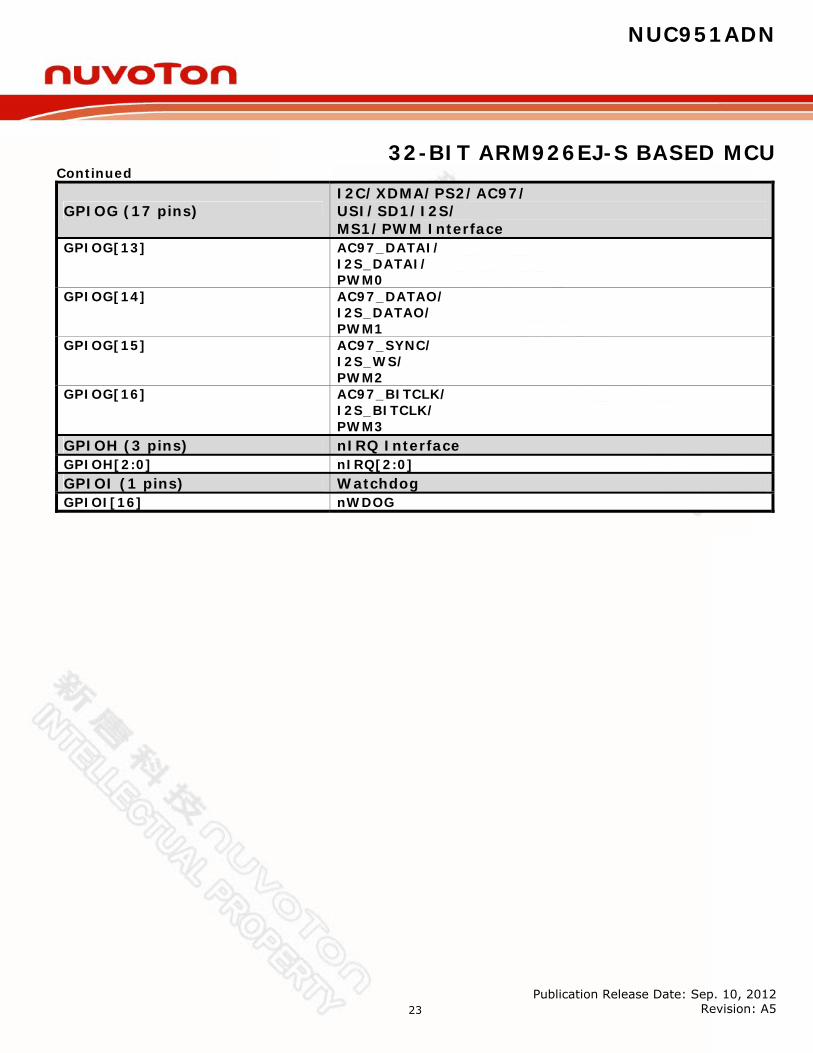
GPIOG (17 pins) I2C/XDMA/PS2/AC97/ USI/SD1/I2S/ MS1/PWM Interface
GPIOG[0] SCL0/ SFRM
GPIOG[1] SDA0/ SSPTXD
GPIOG[2] SCL1/ SCLK
GPIOG[3] SDA1/ SSPRXD
GPIOG[4] nXDREQ0/ SD1_CDn/ MS1_CDn
GPIOG[5] nXDACK0/ SD1_nPWR / MS1_nPWR
GPIOG[6] SD1_CMD/ MS1_BS
GPIOG[7] SD1_CLK/ MS1_CLK
GPIOG[8] PS2CLK0/ SD1_DAT0/ MS1_DAT0
GPIOG[9] PS2DATA0/ SD1_DAT1/ MS1_DAT1
GPIOG[10] PS2CLK1/ SD1_DAT2/ MS1_DAT2
GPIOG[11] PS2DATA1 / SD1_DAT3 / MS1_DAT3
GPIOG[12] AC97_nRESET I2S_SYSCLK
NUC951ADN
32-BIT ARM926EJ-S BASED MCU
Publication Release Date: Sep. 10, 2012 Revision: A5 23
Continued
GPIOG (17 pins) I2C/XDMA/PS2/AC97/ USI/SD1/I2S/ MS1/PWM Interface
GPIOG[13] AC97_DATAI/ I2S_DATAI/ PWM0
GPIOG[14] AC97_DATAO/ I2S_DATAO/ PWM1
GPIOG[15] AC97_SYNC/ I2S_WS/ PWM2
GPIOG[16] AC97_BITCLK/ I2S_BITCLK/ PWM3
GPIOH (3 pins) nIRQ Interface GPIOH[2:0] nIRQ[2:0] GPIOI (1 pins) Watchdog GPIOI[16] nWDOG

NUC951ADN
32-BIT ARM926EJ-S BASED MCU
Publication Release Date: Sep. 10, 2012 Revision: A5 24
6 Functional Block
ARM9EJ-S
MMUICACHE(8KB)
DCACHE(8KB)
ARM926EJ-S
EBI
GDMA2D Graphic Engine
Ethernet MAC
USB 2.0 Host
USB 2.0 Device
LCD Controller
Audio I/FAC97/I2S
DMAC
PLL X 2
CLKGEN
GCR
WDT/TIMER
AIC
PWM(x4)
UART (x3)
PS2(x2)
I2C/SPI
GPIO
RTC
KPI
USB 2.0 Tranceiver
USB 2.0 Tranceiver
AMBA Peripheral
FMI(SD/MS/NAND)
NUC951ADN
NUC951ADN
32-BIT ARM926EJ-S BASED MCU
Publication Release Date: Sep. 10, 2012 Revision: A5 25
7 Functional Description
7.1 ARM926EJ-S CPU CORE The ARM926EJ-S CPU core is a member of the ARM9 family of general-purpose microprocessors. The ARM926EJ-S CPU core supports the 32-bit ARM and 16-bit Thumb instruction sets, enabling the user to trade off between high performance and high code density. The ARM926EJ-S processor has a Harvard cached architecture with MMU.
7.2 System Manager
7.2.1 Overview The System Manager has the following functions. System memory map The width of external memory address Data bus connection with external memory Product identifier register Bus arbitration PLL module Clock select register Power-On setting
7.2.2 System Memory Map This chip provides 2G bytes memory space (0x0000_0000~0x7FFF_FFFF) for the SDRAM, RAM, ROM and IO Devices, 192M bytes space (0xB000_0000~0xBBFF_FFFF) for On-Chip Peripherals and the other memory spaces are reserved. The size and location of each SDRAM memory bank is determined by the register settings for “current bank base address pointer” and “current bank size” (SDCONF0 and SDCONF1). Please note that when setting the bank control registers, the address boundaries of consecutive banks must not be overlapped. Except On-Chip Peripherals, the start address of each memory bank is not fixed. You can use bank control registers to assign a specific bank start address by setting the bank’s base pointer (13 bits). The address resolution is 256K bytes. The bank’s start address is defined as “base pointer << 18” and the bank’s size is “current bank size”. (EXT0CON ~ EXT4CON) The CPU booting start address (from external ROM) is fixed at address 0x0000_0000 after reset or power-on. In the event of an access request to an address outside any programmed bank size, an abort signal is

NUC951ADN
32-BIT ARM926EJ-S BASED MCU
Publication Release Date: Sep. 10, 2012 Revision: A5 26
generated. The maximum accessible memory size of each external IO bank is 32M bytes, and 128M bytes on SDRAM banks.

NUC951ADN
32-BIT ARM926EJ-S BASED MCU
Publication Release Date: Sep. 10, 2012 Revision: A5 27
Address Space Token Modules
0x0000_0000 – 0x7FFF_FFFF ------ EBI(SDRAM, ROM, RAM, IO) Memory Space
0x8000_0000 – 0xAFFF_FFFF ------ Reserved
Shadow of EBI Memory Space(0x0000_0000~0x2FFF_FFFF)
0xB000_0000 – 0xB000_01FF GCR_BA System Global Control Registers
0xB000_0200 – 0xB000_02FF CLK_BA Clock Control Registers
0xB000_1000 – 0xB000_1FFF EBI_BA EBI Control Registers
0xB000_3000 – 0xB000_3FFF EMC_BA Ethernet MAC Control Registers
0xB000_4000 – 0xB000_4FFF GDMA_BA GDMA Control Registers
0xB000_5000 – 0xB000_5FFF USBH_BA EHCI USB Host Control Registers
0xB000_6000 – 0xB000_6FFF USBD_BA USB Device Control Registers
0xB000_7000 – 0xB000_7FFF USBO_BA OHCI USB Host Control Registers
0xB000_8000 – 0xB000_8FFF LCM_BA Display, LCM Interface Control Registers
0xB000_9000 – 0xB000_9FFF ACTL_BA Audio Interface Control Registers
0xB000_A000 – 0xB000_AFFF ------------ Reserved
0xB000_B000 – 0xB000_BFFF GE_BA 2D Graphic Engine Control Register
0xB000_C000 – 0xB000_CFFF DMAC_BA DMA Controller Registers
0xB000_D000 – 0xB000_DFFF FMI_BA Flash Memory Interface Control Registers

NUC951ADN
32-BIT ARM926EJ-S BASED MCU
Publication Release Date: Sep. 10, 2012 Revision: A5 28
Address Space Token Modules
0xB800_0000 – 0xB800_00FF UART0_BA UART 0 Control Registers (Tx,Rx for console)
0xB800_0100 – 0xB800_01FF UART1_BA UART 1 Control Registers (Tx,Rx,CTS,RTS for Blue-tooth)
0xB800_0200 – 0xB800_02FF UART2_BA UART 2 Control Registers (Tx,Rx for IrDA)
0xB800_0300 – 0xB800_03FF ------------ Reserved
0xB800_0400 – 0xB800_04FF ------------ Reserved
0xB800_1000 – 0xB800_1FFF TMR_BA Timer Control Registers
0xB800_2000 – 0xB800_2FFF AIC_BA Interrupt Controller Registers
0xB800_3000 – 0xB800_3FFF GPIO_BA GPIO Control Registers
0xB800_4000 – 0xB800_4FFF RTC_BA Real Time Clock (RTC) Control Registers
0xB800_5000 – 0xB800_5FFF ------------ Reserved
0xB800_6000 – 0xB800_60FF I2C0_BA I2C 0 Control Register
0xB800_6100 – 0xB800_61FF I2C1_BA I2C 1 Control Register
0xB800_6200 – 0xB800_62FF USI_BA Universal Serial Interface Register (USI)
0xB800_7000 – 0xB800_7FFF PWM_BA Pulse Width Modulation(PWM) Control Registers
0xB800_8000 – 0xB800_8FFF KPI_BA Keypad Interface Control Registers
0xB800_9000 – 0xB800_9FFF PS2_BA PS2 Interface Control Registers
NUC951ADN
32-BIT ARM926EJ-S BASED MCU
Publication Release Date: Sep. 10, 2012 Revision: A5 29
7.2.3 Address Bus Generation The address bus generation is depended on the required data bus width (DBWD) and address bus alignment control bit (ADRS) of each IO bank. The maximum accessible memory size of each external IO bank is 32M bytes. (EXT0CON ~ EXT4CON)
Table 7.2.1 Address Bus Generation Guidelines (When ADRS bit = 0)
Data Bus External Address Pins Maximum Accessible
Width MA [21:0] Memory Size
8-bit MA21 – MA0 (Internal) 4M bytes
16-bit MA22 – MA1 (Internal)
8M bytes (4M half-words)
32-bit MA23 – MA2 (Internal)
16M bytes (4M words)
Table 7.2.2 Address Bus Generation Guidelines (When ADRS bit = 1)
Data Bus External Address Pins Maximum Accessible
Width MA [21:0] Memory Size
8-bit MA21 – MA0 (Internal) 4M bytes
16-bit MA21 – MA0 (Internal)
4M bytes, MA[0] ignored (2M half-words)
32-bit MA21 – MA0 (Internal)
4M bytes, MA[1:0] ignored (1M words)

NUC951ADN
32-BIT ARM926EJ-S BASED MCU
Publication Release Date: Sep. 10, 2012 Revision: A5 30
7.2.4 AHB Bus Arbitration The system bus is AHB-compliant and supports modules with standard AHB master or slave interfaces. The AHB arbiter has two priority-decision modes, i.e., the fixed priority mode and the rotate priority mode. In the rotate priority mode, there are three types for AHB-Master bus. The selection of modes and types is determined on the PRTMOD0 and PRTMOD1bits in the Arbitration Control Register. PRTMOD0 is used to control the fixed priority of AHB1 (CPU AHB-Lite) Bus and PRTMOD1 is used to control the fixed priority of AHB2 Master Bus.
7.2.4.1 Fixed Priority Mode Fixed priority mode is selected if PRTMODx = 0. The order of priorities on the AHB mastership among the on-chip master modules, listed in Table 7.2.3, is fixed. If two or more master modules request to AHB at the same time, the mastership is always granted to the module with the highest priority.
Table 7.2.3 AHB Bus Priority Order in Fixed Priority Mode
Priority Sequence
PRTMOD0 = 0 AHB1 Bus
PRTMOD1 = 0 AHB2 Bus
1 (Lowest) ARM CPU Instruction AHB Bridge
2 ARM CPU Data 2-D Graphic
3 GDMA0 ---
4 GDMA1 SDIO(FMI)
5 --- USB Device
6 --- USB Host
7 --- EMC Controller
8 --- LCD Controller
9 (Highest) --- Audio Controller (AC97 & I2S)
The ARM core normally has the lowest priority under the fixed priority mode; however, this chip provides a mechanism to raise the priority to the highest. If the IPEN bit (bit-1 of Arbitration Control Register) is set to 1, the IPACT bit (bit-2 of Arbitration Control Register) will be automatically set to 1 while an unmasked external interrupt occurs. Under this circumstance, the ARM core gains the highest AHB priority. The programmer can recover the original priority order by directly writing “0” to clear the IPACT bit. For example, this can be done that at the end of an interrupt service routine. Note that IPACT only can be automatically set to 1 by an external interrupt when IPEN = 1. It will not take effect if a programmer to directly write 1 to IPACT to raise ARM core’s AHB priority.
NUC951ADN
32-BIT ARM926EJ-S BASED MCU
Publication Release Date: Sep. 10, 2012 Revision: A5 31
7.2.4.2 Rotate Priority Mode Rotate priority mode is selected if PRTMODx = 1. The AHB arbiter uses a round robin arbitration scheme by which every master module can gain the bus ownership in turn. For AHB2 DMA Master Bus, the Audio and LCD Display, have the higher priority in the rotate type.
NUC951ADN
32-BIT ARM926EJ-S BASED MCU
Publication Release Date: Sep. 10, 2012 Revision: A5 32
7.2.5 Power-On Setting After power on reset, Power-On setting registers are latched from EBI Address pins (MA [21:13]) to configure this chip. Power-On Setting Pin Booting Device Select MA [21:20] USB PLL Clock Source Select MA19 Internal System Clock Select MA17 GPIO Pin Configuration Select MA [16:14] USB PHY0 Mode Select HDS MA [21:20] : Booting Device Select
MA[21:20] Booting Device Pull-down Pull-down SPI Flash ROM Pull-down Pull-up NAND-type Flash ROM
Pull-up Pull-down USB ISP Pull-up Pull-up NOR-type Flash ROM
MA19 : USB PLL Clock Source Select
MA19 Clock Source Pull-down Oscillator
Pull-up Crystal MA18 :Can either Pull-up or Pull-down MA17 :Internal System Clock Select If pin MA17 is pull-down, the external clock from EXTAL15M pin is served as internal system clock. If pin MA17 is pull-up, the PLL output clock is used as internal system clock. MA [16:14] : GPIO Pin Configuration Select
MA[16:14] State GPIO Pin Function
MA14 Pull-down GPIOC/D/E Group Select Pull-up NAND/UART Group Select
MA15 Pull-down GPIOF Group Select Pull-up RMII Group Select
MA16 Pull-down GPIOI/KPI Group Select Pull-up Reserved
MA13 :Pull-up is necessary HDS: USB PHY0 Mode Select

NUC951ADN
32-BIT ARM926EJ-S BASED MCU
Publication Release Date: Sep. 10, 2012 Revision: A5 33
HDS USB PHY0 Mode Pull-down USB20 Host
Pull-up USB20 Device
7.2.6 System Booting
NUC910ABN supports four kinds of system booting devices, which including (1) SPI Flash ROM (2) NAND-type Flash ROM (3) USB ISP (4) NOR-type Flash ROM Booting Device Select
MA[21:20] Booting Device Pull-down Pull-down SPI Flash ROM Pull-down Pull-up NAND-type Flash ROM
Pull-up Pull-down USB ISP Pull-up Pull-up NOR-type Flash ROM

NUC951ADN
32-BIT ARM926EJ-S BASED MCU
Publication Release Date: Sep. 10, 2012 Revision: A5 34
7.2.7 System Global Control Registers Map
Register Address R/W Description Reset Value
GCR_BA = 0xB000_0000
PDID 0xB000_0000 R Product Identifier Register 0xxx90_0910
PWRON 0xB000_0004 R/W Power-On Setting Register N/A
ARBCON 0xB000_0008 R/W Arbitration Control Register 0x0000_0000
MFSEL 0xB000_000C R/W Multiple Function Pin Select Register 0x0800_0000
EBIDPE 0xB000_0010 R/W EBI Data Pin Pull-up/down Enable Register 0xFFFF_FFFF
LCDDPE 0xB000_0014 R/W LCD Data Pin Pull-up/down Enable Register 0x0003_FFFF
GPIOCPE 0xB000_0018 R/W GPIOC Pin Pull-up/down Enable Register 0x0000_7FFF
GPIODPE 0xB000_001C R/W GPIOD Pin Pull-up/down Enable Register 0x0000_07FF
GPIOEPE 0xB000_0020 R/W GPIOE Pin Pull-up/down Enable Register 0x0000_3FFF
GPIOFPE 0xB000_0024 R/W GPIOF Pin Pull-up/down Enable Register 0x0000_03FF
GPIOGPE 0xB000_0028 R/W GPIOG Pin Pull-up/down Enable Register 0x0001_FFFF
GPIOHPE 0xB000_002C R/W GPIOH Pin Pull-up/down Enable Register 0x0000_00FF
GPIOIPE 0xB000_0030 R/W GPIOI Pin Pull-up/down Enable Register 0x0FFF_FFFF
GTMP1 0xB000_0034 R/W General Temporary Register 1 N/A
GTMP2 0xB000_0038 R/W General Temporary Register 2 N/A
GTMP3 0xB000_003C R/W General Temporary Register 3 N/A

NUC951ADN
32-BIT ARM926EJ-S BASED MCU
Publication Release Date: Sep. 10, 2012 Revision: A5 35
Product Identifier Register (PDID)
This register is for only read and enables software to recognize certain characteristics of the chip ID and the version number.
Register Address R/W Description Reset Value
PDID 0xB000_0000 R Product Identifier Register 0xxx90_0910
31 30 29 28 27 26 25 24 VERSION
23 22 21 20 19 18 17 16 CHPID
15 14 13 12 11 10 9 8 CHPID
7 6 5 4 3 2 1 0 CHPID
Bits Descriptions
[31:24] VERSION Version of chip 02: Version C
[23:0] CHIPID Chip identifier The NUC910ABN Chip identifier is 0x90_0910.
NUC951ADN
32-BIT ARM926EJ-S BASED MCU
Publication Release Date: Sep. 10, 2012 Revision: A5 36
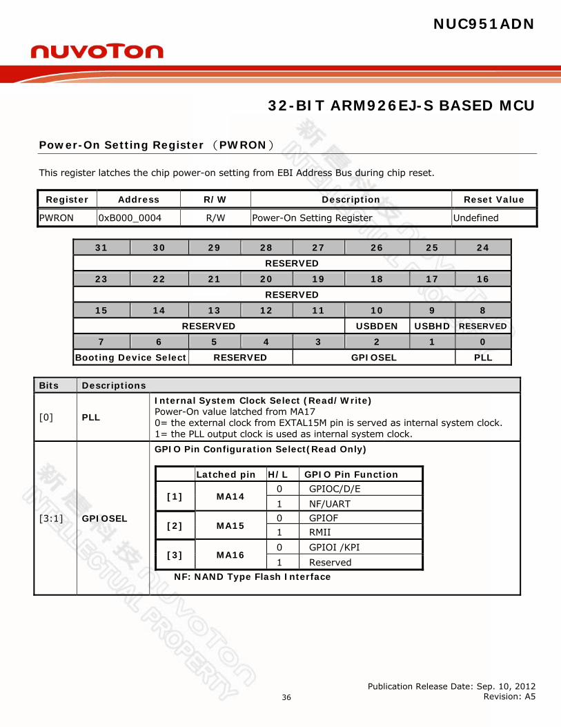
Power-On Setting Register (PWRON)
This register latches the chip power-on setting from EBI Address Bus during chip reset.
Register Address R/W Description Reset Value
PWRON 0xB000_0004 R/W Power-On Setting Register Undefined
31 30 29 28 27 26 25 24 RESERVED
23 22 21 20 19 18 17 16 RESERVED
15 14 13 12 11 10 9 8 RESERVED USBDEN USBHD RESERVED
7 6 5 4 3 2 1 0 Booting Device Select RESERVED GPIOSEL PLL
Bits Descriptions
[0] PLL
Internal System Clock Select (Read/Write) Power-On value latched from MA17 0= the external clock from EXTAL15M pin is served as internal system clock. 1= the PLL output clock is used as internal system clock.
[3:1] GPIOSEL
GPIO Pin Configuration Select(Read Only) Latched pin H/L GPIO Pin Function
[1] MA14 0 GPIOC/D/E 1 NF/UART
[2] MA15 0 GPIOF 1 RMII
[3] MA16 0 GPIOI /KPI 1 Reserved
NF: NAND Type Flash Interface
NUC951ADN
32-BIT ARM926EJ-S BASED MCU
Publication Release Date: Sep. 10, 2012 Revision: A5 37
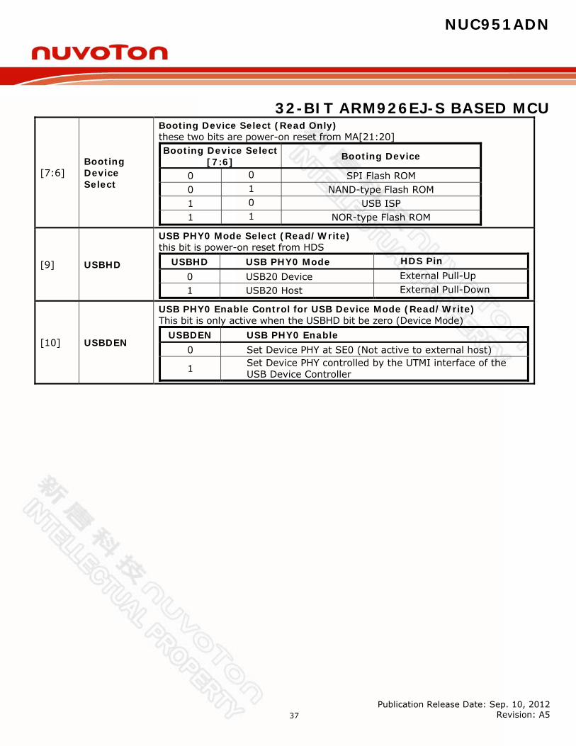
[7:6] Booting Device Select
Booting Device Select (Read Only) these two bits are power-on reset from MA[21:20] Booting Device Select
[7:6] Booting Device
0 0 SPI Flash ROM 0 1 NAND-type Flash ROM 1 0 USB ISP 1 1 NOR-type Flash ROM
[9] USBHD
USB PHY0 Mode Select (Read/Write) this bit is power-on reset from HDS
USBHD USB PHY0 Mode HDS Pin 0 USB20 Device External Pull-Up 1 USB20 Host External Pull-Down
[10] USBDEN
USB PHY0 Enable Control for USB Device Mode (Read/Write) This bit is only active when the USBHD bit be zero (Device Mode)
USBDEN USB PHY0 Enable 0 Set Device PHY at SE0 (Not active to external host)
1 Set Device PHY controlled by the UTMI interface of the USB Device Controller
NUC951ADN
32-BIT ARM926EJ-S BASED MCU
Publication Release Date: Sep. 10, 2012 Revision: A5 38
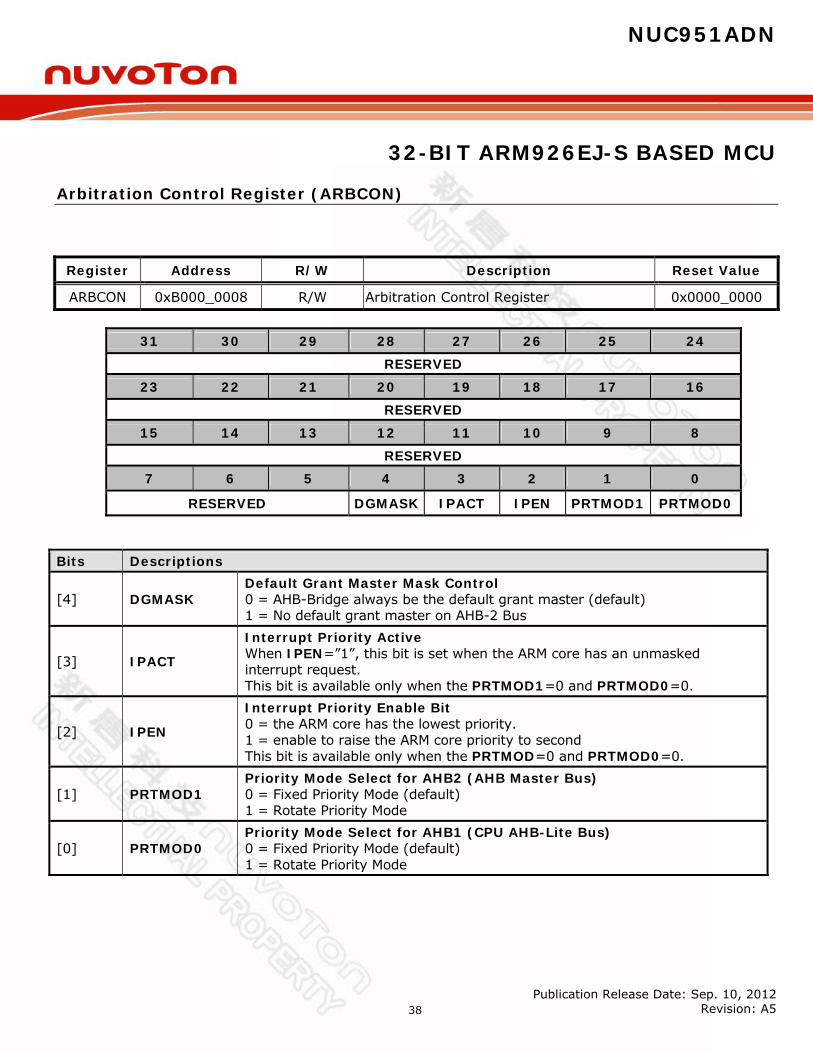
Arbitration Control Register (ARBCON)
Register Address R/W Description Reset Value
ARBCON 0xB000_0008 R/W Arbitration Control Register 0x0000_0000
31 30 29 28 27 26 25 24 RESERVED
23 22 21 20 19 18 17 16 RESERVED
15 14 13 12 11 10 9 8 RESERVED
7 6 5 4 3 2 1 0
RESERVED DGMASK IPACT IPEN PRTMOD1 PRTMOD0 Bits Descriptions
[4] DGMASK Default Grant Master Mask Control 0 = AHB-Bridge always be the default grant master (default) 1 = No default grant master on AHB-2 Bus
[3] IPACT
Interrupt Priority Active When IPEN=”1”, this bit is set when the ARM core has an unmasked interrupt request. This bit is available only when the PRTMOD1=0 and PRTMOD0=0.
[2] IPEN
Interrupt Priority Enable Bit 0 = the ARM core has the lowest priority. 1 = enable to raise the ARM core priority to second This bit is available only when the PRTMOD=0 and PRTMOD0=0.
[1] PRTMOD1 Priority Mode Select for AHB2 (AHB Master Bus) 0 = Fixed Priority Mode (default) 1 = Rotate Priority Mode
[0] PRTMOD0 Priority Mode Select for AHB1 (CPU AHB-Lite Bus) 0 = Fixed Priority Mode (default) 1 = Rotate Priority Mode
NUC951ADN
32-BIT ARM926EJ-S BASED MCU
Publication Release Date: Sep. 10, 2012 Revision: A5 39
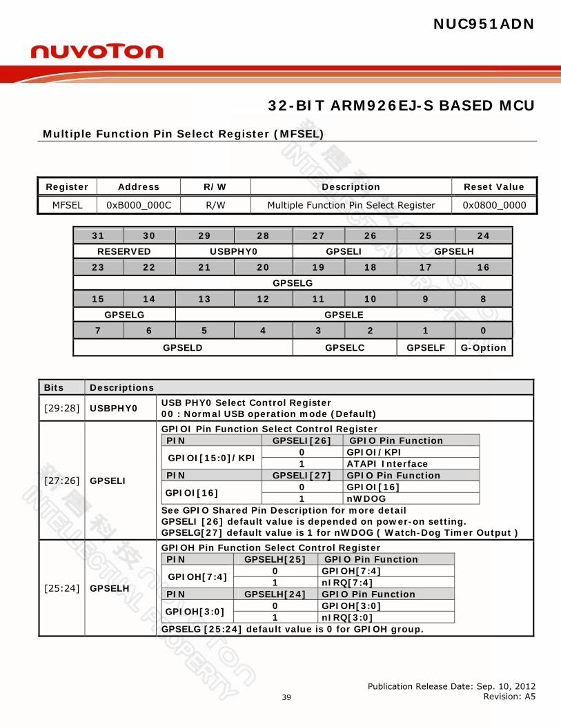
Multiple Function Pin Select Register (MFSEL)
Register Address R/W Description Reset Value
MFSEL 0xB000_000C R/W Multiple Function Pin Select Register 0x0800_0000
31 30 29 28 27 26 25 24 RESERVED USBPHY0 GPSELI GPSELH
23 22 21 20 19 18 17 16 GPSELG
15 14 13 12 11 10 9 8 GPSELG GPSELE
7 6 5 4 3 2 1 0
GPSELD GPSELC GPSELF G-Option Bits Descriptions
[29:28] USBPHY0 USB PHY0 Select Control Register 00 : Normal USB operation mode (Default)
[27:26] GPSELI
GPIOI Pin Function Select Control Register PIN GPSELI[26] GPIO Pin Function
GPIOI[15:0]/KPI 0 GPIOI/KPI 1 ATAPI Interface
PIN GPSELI[27] GPIO Pin Function
GPIOI[16] 0 GPIOI[16] 1 nWDOG
See GPIO Shared Pin Description for more detail GPSELI [26] default value is depended on power-on setting. GPSELG[27] default value is 1 for nWDOG ( Watch-Dog Timer Output )
[25:24] GPSELH
GPIOH Pin Function Select Control Register PIN GPSELH[25] GPIO Pin Function
GPIOH[7:4] 0 GPIOH[7:4] 1 nIRQ[7:4]
PIN GPSELH[24] GPIO Pin Function
GPIOH[3:0] 0 GPIOH[3:0] 1 nIRQ[3:0]
GPSELG [25:24] default value is 0 for GPIOH group.
NUC951ADN
32-BIT ARM926EJ-S BASED MCU
Publication Release Date: Sep. 10, 2012 Revision: A5 40
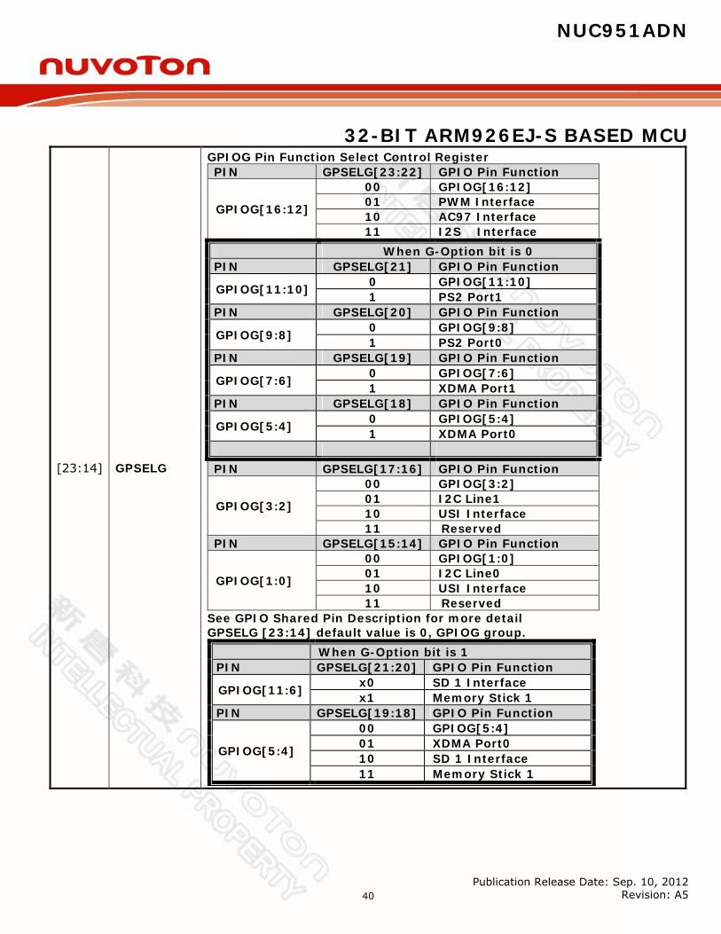
[23:14] GPSELG
GPIOG Pin Function Select Control Register PIN GPSELG[23:22] GPIO Pin Function
GPIOG[16:12]
00 GPIOG[16:12] 01 PWM Interface 10 AC97 Interface 11 I2S Interface
When G-Option bit is 0 PIN GPSELG[21] GPIO Pin Function
GPIOG[11:10] 0 GPIOG[11:10] 1 PS2 Port1
PIN GPSELG[20] GPIO Pin Function
GPIOG[9:8] 0 GPIOG[9:8] 1 PS2 Port0
PIN GPSELG[19] GPIO Pin Function
GPIOG[7:6] 0 GPIOG[7:6] 1 XDMA Port1
PIN GPSELG[18] GPIO Pin Function
GPIOG[5:4] 0 GPIOG[5:4] 1 XDMA Port0
PIN GPSELG[17:16] GPIO Pin Function
GPIOG[3:2]
00 GPIOG[3:2] 01 I2C Line1 10 USI Interface 11 Reserved
PIN GPSELG[15:14] GPIO Pin Function
GPIOG[1:0]
00 GPIOG[1:0] 01 I2C Line0 10 USI Interface 11 Reserved
See GPIO Shared Pin Description for more detail GPSELG [23:14] default value is 0, GPIOG group.
When G-Option bit is 1 PIN GPSELG[21:20] GPIO Pin Function
GPIOG[11:6] x0 SD 1 Interface x1 Memory Stick 1
PIN GPSELG[19:18] GPIO Pin Function
GPIOG[5:4]
00 GPIOG[5:4] 01 XDMA Port0 10 SD 1 Interface 11 Memory Stick 1
NUC951ADN
32-BIT ARM926EJ-S BASED MCU
Publication Release Date: Sep. 10, 2012 Revision: A5 41
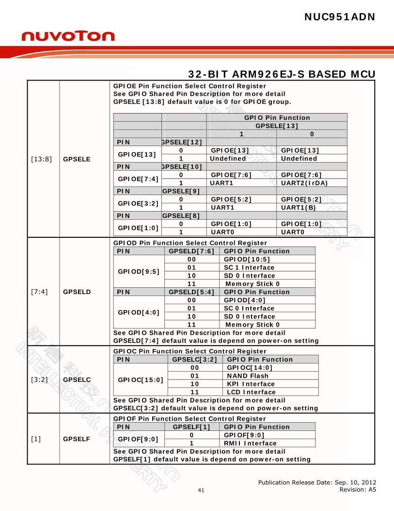
[13:8] GPSELE
GPIOE Pin Function Select Control Register See GPIO Shared Pin Description for more detail GPSELE [13:8] default value is 0 for GPIOE group. GPIO Pin Function GPSELE[13] 1 0 PIN GPSELE[12]
GPIOE[13] 0 GPIOE[13] GPIOE[13] 1 Undefined Undefined
PIN GPSELE[10]
GPIOE[7:4] 0 GPIOE[7:6] GPIOE[7:6] 1 UART1 UART2(IrDA)
PIN GPSELE[9]
GPIOE[3:2] 0 GPIOE[5:2] GPIOE[5:2] 1 UART1 UART1(B)
PIN GPSELE[8]
GPIOE[1:0] 0 GPIOE[1:0] GPIOE[1:0] 1 UART0 UART0
[7:4] GPSELD
GPIOD Pin Function Select Control Register PIN GPSELD[7:6] GPIO Pin Function
GPIOD[9:5]
00 GPIOD[10:5] 01 SC 1 Interface 10 SD 0 Interface 11 Memory Stick 0
PIN GPSELD[5:4] GPIO Pin Function
GPIOD[4:0]
00 GPIOD[4:0] 01 SC 0 Interface 10 SD 0 Interface 11 Memory Stick 0
See GPIO Shared Pin Description for more detail GPSELD[7:4] default value is depend on power-on setting
[3:2] GPSELC
GPIOC Pin Function Select Control Register PIN GPSELC[3:2] GPIO Pin Function
GPIOC[15:0]
00 GPIOC[14:0] 01 NAND Flash 10 KPI Interface 11 LCD Interface
See GPIO Shared Pin Description for more detail GPSELC[3:2] default value is depend on power-on setting
[1] GPSELF
GPIOF Pin Function Select Control Register PIN GPSELF[1] GPIO Pin Function
GPIOF[9:0] 0 GPIOF[9:0] 1 RMII Interface
See GPIO Shared Pin Description for more detail GPSELF[1] default value is depend on power-on setting
NUC951ADN
32-BIT ARM926EJ-S BASED MCU
Publication Release Date: Sep. 10, 2012 Revision: A5 42
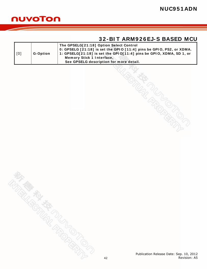
[0] G-Option
The GPSELG[21:18] Option Select Control 0: GPSELG [21:18] is set the GPIO [11:4] pins be GPIO, PS2, or XDMA. 1: GPSELG[21:18] is set the GPIO[11:4] pins be GPIO, XDMA, SD 1, or
Memory Stick 1 Interface, See GPSELG description for more detail.

NUC951ADN
32-BIT ARM926EJ-S BASED MCU
Publication Release Date: Sep. 10, 2012 Revision: A5 43
EBI Data Pin Pull-up/down Enable Register (EBIDPE)
LCD Data Pin Pull-up/down Enable Register (LCDDPE)
GPIOC~GPIOI Pin Pull-up/down Enable Register (GPIOCPE~GPIOIPE)
These registers are used to control the IO pins to be internal pull-up or down, which can avoid the input pins floating if there is no external resistors.
Register Address R/W Description Reset Value
EBIDPE 0xB000_0010 R/W EBI Data Pin Pull-down Enable Register 0xFFFF_FFFF
LCDDPE 0xB000_0014 R/W LCD Data Pin Pull-up Enable Register 0x0003_FFFF
GPIOCPE 0xB000_0018 R/W GPIOC Pin Pull-up Enable Register 0x0000_FFFF
GPIODPE 0xB000_001C R/W GPIOD Pin Pull-up Enable Register 0x0000_07FF
GPIOEPE 0xB000_0020 R/W GPIOE Pin Pull-up/down Enable Register 0x0000_3FFF
GPIOFPE 0xB000_0024 R/W GPIOF Pin Pull-up/down Enable Register 0x0000_03FF
GPIOGPE 0xB000_0028 R/W GPIOG Pin Pull-up/down Enable Register 0x0001_FFFF
GPIOHPE 0xB000_002C R/W GPIOH Pin Pull-up Enable Register 0x0000_00FF
GPIOIPE 0xB000_0030 R/W GPIOI Pin Pull-up/down Enable Register 0x0FFF_FFFF
31 30 29 28 27 26 25 24 PPE
23 22 21 20 19 18 17 16 PPE
15 14 13 12 11 10 9 8 PPE
7 6 5 4 3 2 1 0 PPE
Bits Descriptions
[31:0] PPE Pin Pull-down Enable Register 1 = Disable the Pull-high/down for each relative pin (default) 0 = Enable the Pull-high/down for each relative pin
NUC951ADN
32-BIT ARM926EJ-S BASED MCU
Publication Release Date: Sep. 10, 2012 Revision: A5 44
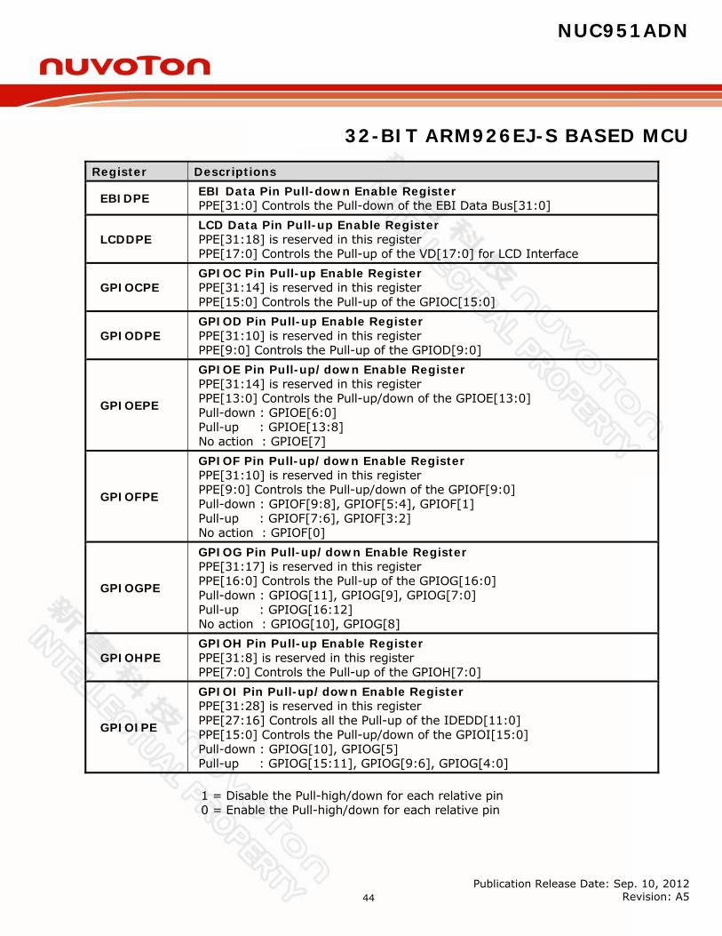
Register Descriptions
EBIDPE EBI Data Pin Pull-down Enable Register PPE[31:0] Controls the Pull-down of the EBI Data Bus[31:0]
LCDDPE LCD Data Pin Pull-up Enable Register PPE[31:18] is reserved in this register PPE[17:0] Controls the Pull-up of the VD[17:0] for LCD Interface
GPIOCPE GPIOC Pin Pull-up Enable Register PPE[31:14] is reserved in this register PPE[15:0] Controls the Pull-up of the GPIOC[15:0]
GPIODPE GPIOD Pin Pull-up Enable Register PPE[31:10] is reserved in this register PPE[9:0] Controls the Pull-up of the GPIOD[9:0]
GPIOEPE
GPIOE Pin Pull-up/down Enable Register PPE[31:14] is reserved in this register PPE[13:0] Controls the Pull-up/down of the GPIOE[13:0] Pull-down : GPIOE[6:0] Pull-up : GPIOE[13:8] No action : GPIOE[7]
GPIOFPE
GPIOF Pin Pull-up/down Enable Register PPE[31:10] is reserved in this register PPE[9:0] Controls the Pull-up/down of the GPIOF[9:0] Pull-down : GPIOF[9:8], GPIOF[5:4], GPIOF[1] Pull-up : GPIOF[7:6], GPIOF[3:2] No action : GPIOF[0]
GPIOGPE
GPIOG Pin Pull-up/down Enable Register PPE[31:17] is reserved in this register PPE[16:0] Controls the Pull-up of the GPIOG[16:0] Pull-down : GPIOG[11], GPIOG[9], GPIOG[7:0] Pull-up : GPIOG[16:12] No action : GPIOG[10], GPIOG[8]
GPIOHPE GPIOH Pin Pull-up Enable Register PPE[31:8] is reserved in this register PPE[7:0] Controls the Pull-up of the GPIOH[7:0]
GPIOIPE
GPIOI Pin Pull-up/down Enable Register PPE[31:28] is reserved in this register PPE[27:16] Controls all the Pull-up of the IDEDD[11:0] PPE[15:0] Controls the Pull-up/down of the GPIOI[15:0] Pull-down : GPIOG[10], GPIOG[5] Pull-up : GPIOG[15:11], GPIOG[9:6], GPIOG[4:0]
1 = Disable the Pull-high/down for each relative pin 0 = Enable the Pull-high/down for each relative pin
NUC951ADN
32-BIT ARM926EJ-S BASED MCU
Publication Release Date: Sep. 10, 2012 Revision: A5 45
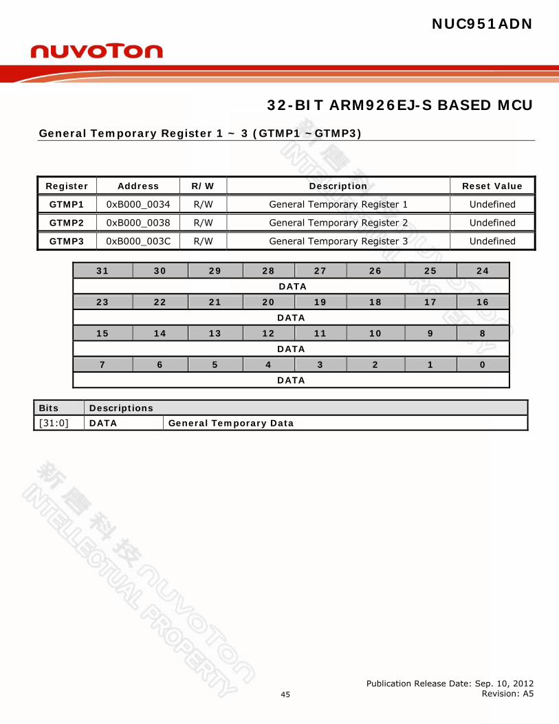
General Temporary Register 1 ~ 3 (GTMP1 ~GTMP3)
Register Address R/W Description Reset Value
GTMP1 0xB000_0034 R/W General Temporary Register 1 Undefined
GTMP2 0xB000_0038 R/W General Temporary Register 2 Undefined
GTMP3 0xB000_003C R/W General Temporary Register 3 Undefined
31 30 29 28 27 26 25 24 DATA
23 22 21 20 19 18 17 16 DATA
15 14 13 12 11 10 9 8 DATA
7 6 5 4 3 2 1 0 DATA
Bits Descriptions [31:0] DATA General Temporary Data
NUC951ADN
32-BIT ARM926EJ-S BASED MCU
Publication Release Date: Sep. 10, 2012 Revision: A5 46
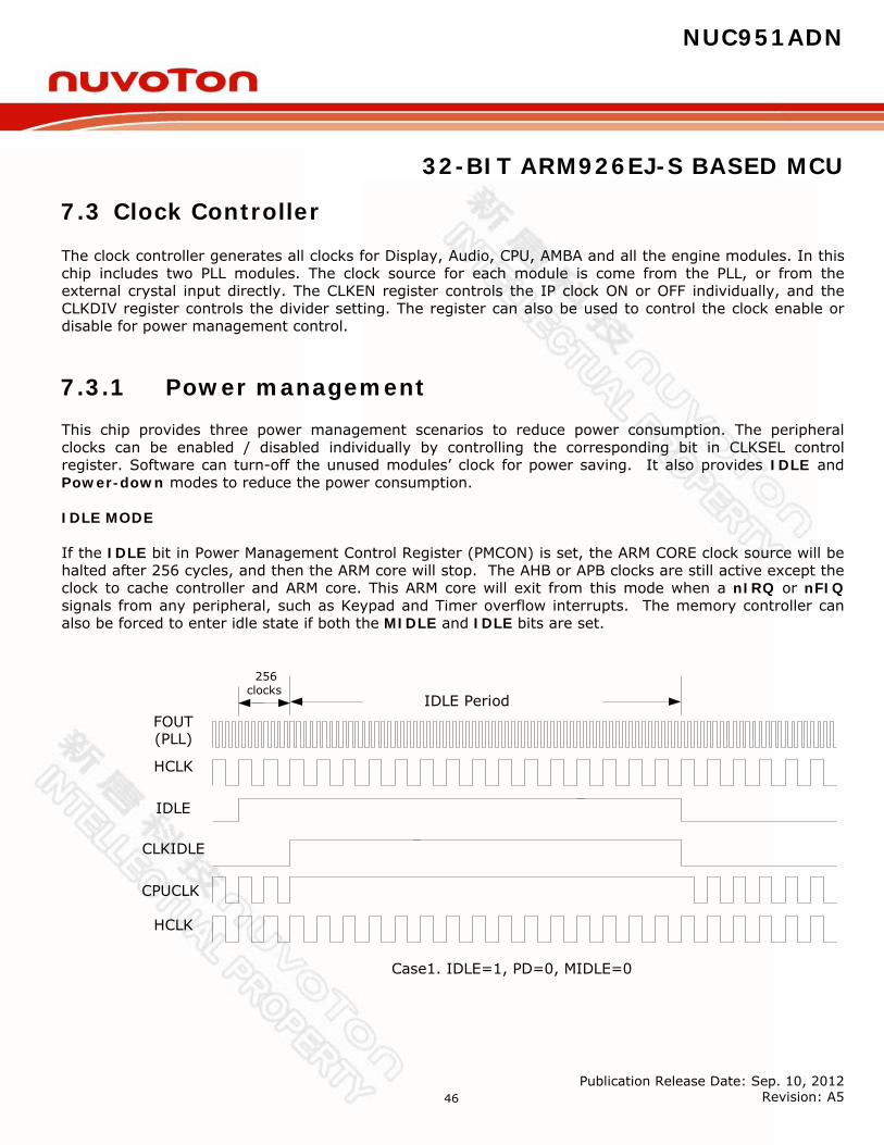
7.3 Clock Controller The clock controller generates all clocks for Display, Audio, CPU, AMBA and all the engine modules. In this chip includes two PLL modules. The clock source for each module is come from the PLL, or from the external crystal input directly. The CLKEN register controls the IP clock ON or OFF individually, and the CLKDIV register controls the divider setting. The register can also be used to control the clock enable or disable for power management control.
7.3.1 Power management This chip provides three power management scenarios to reduce power consumption. The peripheral clocks can be enabled / disabled individually by controlling the corresponding bit in CLKSEL control register. Software can turn-off the unused modules’ clock for power saving. It also provides IDLE and Power-down modes to reduce the power consumption. IDLE MODE If the IDLE bit in Power Management Control Register (PMCON) is set, the ARM CORE clock source will be halted after 256 cycles, and then the ARM core will stop. The AHB or APB clocks are still active except the clock to cache controller and ARM core. This ARM core will exit from this mode when a nIRQ or nFIQ signals from any peripheral, such as Keypad and Timer overflow interrupts. The memory controller can also be forced to enter idle state if both the MIDLE and IDLE bits are set.
FOUT(PLL)
HCLK
IDLE
CPUCLK
IDLE Period
HCLK
Case1. IDLE=1, PD=0, MIDLE=0
CLKIDLE
256clocks
NUC951ADN
32-BIT ARM926EJ-S BASED MCU
Publication Release Date: Sep. 10, 2012 Revision: A5 47
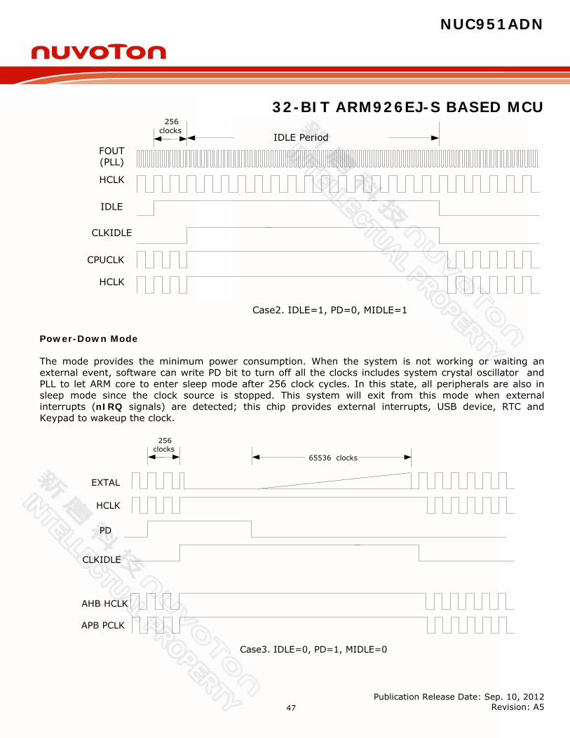
FOUT(PLL)
HCLK
IDLE
CPUCLK
IDLE Period
HCLK
Case2. IDLE=1, PD=0, MIDLE=1
CLKIDLE
256clocks
Power-Down Mode The mode provides the minimum power consumption. When the system is not working or waiting an external event, software can write PD bit to turn off all the clocks includes system crystal oscillator and PLL to let ARM core to enter sleep mode after 256 clock cycles. In this state, all peripherals are also in sleep mode since the clock source is stopped. This system will exit from this mode when external interrupts (nIRQ signals) are detected; this chip provides external interrupts, USB device, RTC and Keypad to wakeup the clock.
AHB HCLK
Case3. IDLE=0, PD=1, MIDLE=0
EXTAL
PD
CLKIDLE
65536 clocks
HCLK
256clocks
APB PCLK
NUC951ADN
32-BIT ARM926EJ-S BASED MCU
Publication Release Date: Sep. 10, 2012 Revision: A5 48
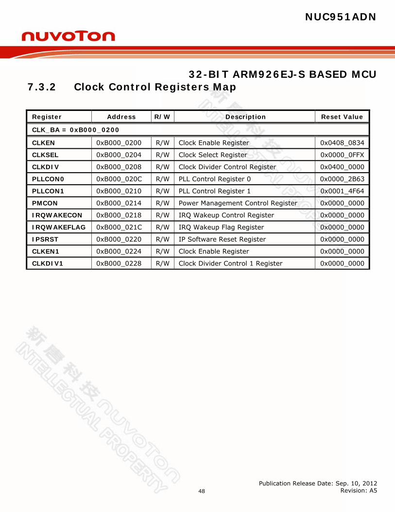
7.3.2 Clock Control Registers Map
Register Address R/W Description Reset Value
CLK_BA = 0xB000_0200
CLKEN 0xB000_0200 R/W Clock Enable Register 0x0408_0834
CLKSEL 0xB000_0204 R/W Clock Select Register 0x0000_0FFX
CLKDIV 0xB000_0208 R/W Clock Divider Control Register 0x0400_0000
PLLCON0 0xB000_020C R/W PLL Control Register 0 0x0000_2B63
PLLCON1 0xB000_0210 R/W PLL Control Register 1 0x0001_4F64
PMCON 0xB000_0214 R/W Power Management Control Register 0x0000_0000
IRQWAKECON 0xB000_0218 R/W IRQ Wakeup Control Register 0x0000_0000
IRQWAKEFLAG 0xB000_021C R/W IRQ Wakeup Flag Register 0x0000_0000
IPSRST 0xB000_0220 R/W IP Software Reset Register 0x0000_0000
CLKEN1 0xB000_0224 R/W Clock Enable Register 0x0000_0000
CLKDIV1 0xB000_0228 R/W Clock Divider Control 1 Register 0x0000_0000
NUC951ADN
32-BIT ARM926EJ-S BASED MCU
Publication Release Date: Sep. 10, 2012 Revision: A5 49
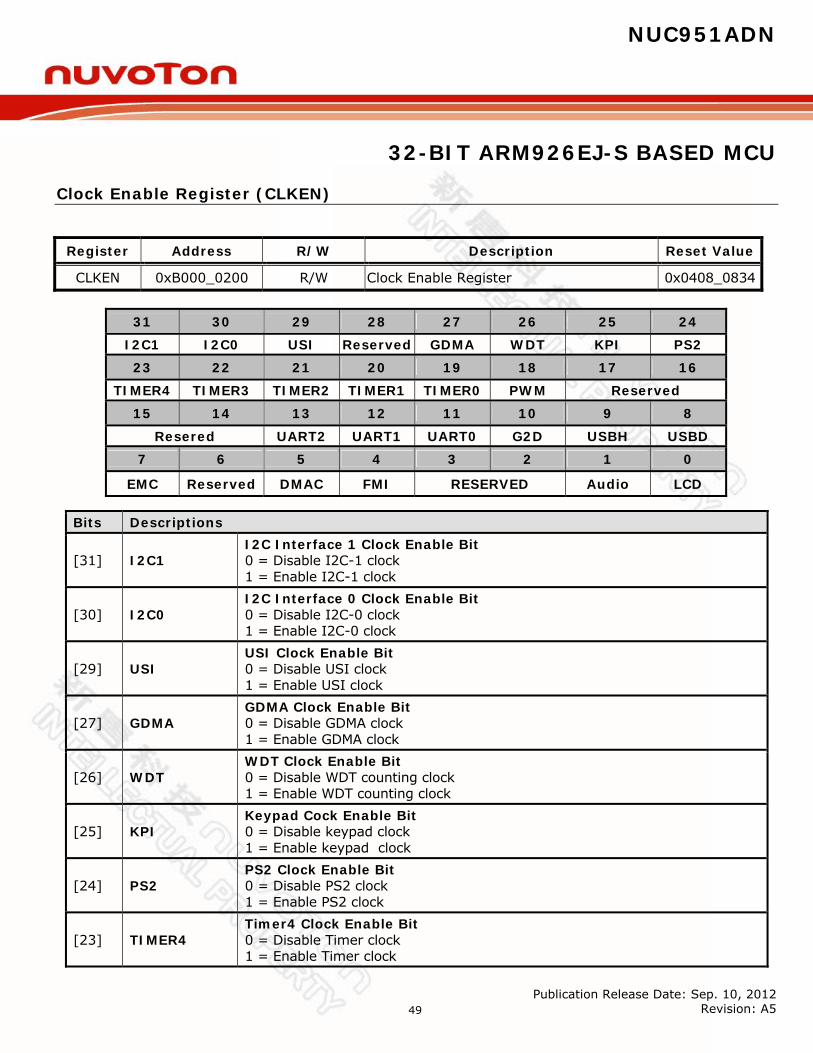
Clock Enable Register (CLKEN)
Register Address R/W Description Reset Value
CLKEN 0xB000_0200 R/W Clock Enable Register 0x0408_0834
31 30 29 28 27 26 25 24 I2C1 I2C0 USI Reserved GDMA WDT KPI PS2 23 22 21 20 19 18 17 16
TIMER4 TIMER3 TIMER2 TIMER1 TIMER0 PWM Reserved 15 14 13 12 11 10 9 8
Resered UART2 UART1 UART0 G2D USBH USBD 7 6 5 4 3 2 1 0
EMC Reserved DMAC FMI RESERVED Audio LCD
Bits Descriptions
[31] I2C1 I2C Interface 1 Clock Enable Bit 0 = Disable I2C-1 clock 1 = Enable I2C-1 clock
[30] I2C0 I2C Interface 0 Clock Enable Bit 0 = Disable I2C-0 clock 1 = Enable I2C-0 clock
[29] USI USI Clock Enable Bit 0 = Disable USI clock 1 = Enable USI clock
[27] GDMA GDMA Clock Enable Bit 0 = Disable GDMA clock 1 = Enable GDMA clock
[26] WDT WDT Clock Enable Bit 0 = Disable WDT counting clock 1 = Enable WDT counting clock
[25] KPI Keypad Cock Enable Bit 0 = Disable keypad clock 1 = Enable keypad clock
[24] PS2 PS2 Clock Enable Bit 0 = Disable PS2 clock 1 = Enable PS2 clock
[23] TIMER4 Timer4 Clock Enable Bit 0 = Disable Timer clock 1 = Enable Timer clock
NUC951ADN
32-BIT ARM926EJ-S BASED MCU
Publication Release Date: Sep. 10, 2012 Revision: A5 50
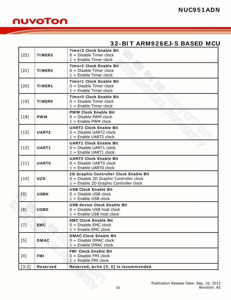
[22] TIMER3 Timer3 Clock Enable Bit 0 = Disable Timer clock 1 = Enable Timer clock
[21] TIMER2 Timer2 Clock Enable Bit 0 = Disable Timer clock 1 = Enable Timer clock
[20] TIMER1 Timer1 Clock Enable Bit 0 = Disable Timer clock 1 = Enable Timer clock
[19] TIMER0 Timer0 Clock Enable Bit 0 = Disable Timer clock 1 = Enable Timer clock
[18] PWM PWM Clock Enable Bit 0 = Disable PWM clock 1 = Enable PWM clock
[13] UART2 UART2 Clock Enable Bit 0 = Disable UART2 clock 1 = Enable UART2 clock
[12] UART1 UART1 Clock Enable Bit 0 = Disable UART1 clock 1 = Enable UART1 clock
[11] UART0 UART0 Clock Enable Bit 0 = Disable UART0 clock 1 = Enable UART0 clock
[10] G2D 2D Graphic Controller Clock Enable Bit 0 = Disable 2D Graphic Controller clock 1 = Enable 2D Graphic Controller clock
[9] USBH USB Clock Enable Bit 0 = Disable USB clock 1 = Enable USB clock
[8] USBD USB device Clock Enable Bit 0 = Disable USB host clock 1 = Enable USB host clock
[7] EMC EMC Clock Enable Bit 0 = Disable EMC clock 1 = Enable EMC clock
[5] DMAC DMAC Clock Enable Bit 0 = Disable DMAC clock 1 = Enable DMAC clock
[4] FMI FMI Clock Enable Bit 0 = Disable FMI clock 1 = Enable FMI clock
[3:2] Reserved Reserved, write [0, 0] is recommended.
NUC951ADN
32-BIT ARM926EJ-S BASED MCU
Publication Release Date: Sep. 10, 2012 Revision: A5 51
[1] Audio Audio Controller Clock Enable Bit 0 = Disable Audio Controller clock 1 = Enable Audio Controller clock
[0] LCD LCD Clock Enable Bit 0 = Disable LCD clock 1 = Enable LCD clock
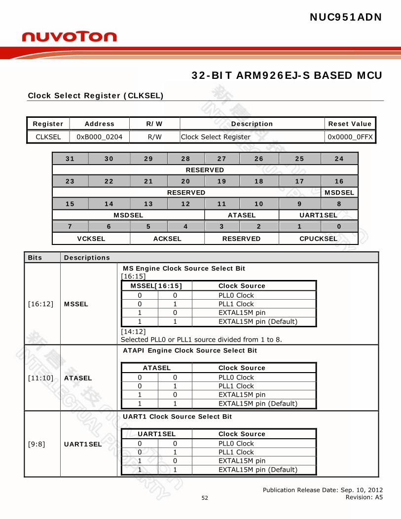
NUC951ADN
32-BIT ARM926EJ-S BASED MCU
Publication Release Date: Sep. 10, 2012 Revision: A5 52
Clock Select Register (CLKSEL)
Register Address R/W Description Reset Value
CLKSEL 0xB000_0204 R/W Clock Select Register 0x0000_0FFX
31 30 29 28 27 26 25 24 RESERVED
23 22 21 20 19 18 17 16 RESERVED MSDSEL
15 14 13 12 11 10 9 8 MSDSEL ATASEL UART1SEL
7 6 5 4 3 2 1 0 VCKSEL ACKSEL RESERVED CPUCKSEL
Bits Descriptions
[16:12] MSSEL
MS Engine Clock Source Select Bit [16:15]
MSSEL[16:15] Clock Source 0 0 PLL0 Clock 0 1 PLL1 Clock 1 0 EXTAL15M pin 1 1 EXTAL15M pin (Default)
[14:12] Selected PLL0 or PLL1 source divided from 1 to 8.
[11:10] ATASEL
ATAPI Engine Clock Source Select Bit
ATASEL Clock Source 0 0 PLL0 Clock 0 1 PLL1 Clock 1 0 EXTAL15M pin 1 1 EXTAL15M pin (Default)
[9:8] UART1SEL
UART1 Clock Source Select Bit
UART1SEL Clock Source 0 0 PLL0 Clock 0 1 PLL1 Clock 1 0 EXTAL15M pin 1 1 EXTAL15M pin (Default)
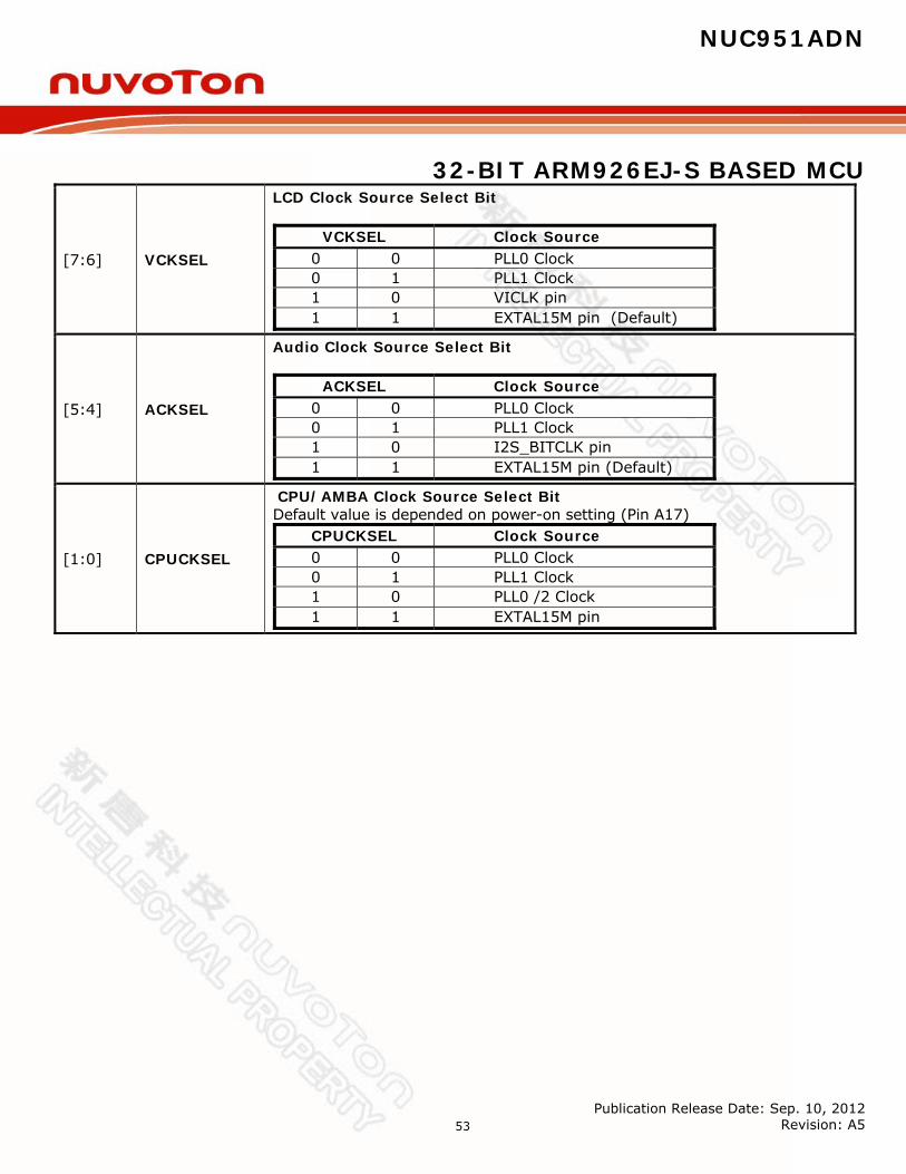
NUC951ADN
32-BIT ARM926EJ-S BASED MCU
Publication Release Date: Sep. 10, 2012 Revision: A5 53
[7:6] VCKSEL
LCD Clock Source Select Bit
VCKSEL Clock Source 0 0 PLL0 Clock 0 1 PLL1 Clock 1 0 VICLK pin 1 1 EXTAL15M pin (Default)
[5:4] ACKSEL
Audio Clock Source Select Bit
ACKSEL Clock Source 0 0 PLL0 Clock 0 1 PLL1 Clock 1 0 I2S_BITCLK pin 1 1 EXTAL15M pin (Default)
[1:0] CPUCKSEL
CPU/AMBA Clock Source Select Bit Default value is depended on power-on setting (Pin A17)
CPUCKSEL Clock Source 0 0 PLL0 Clock 0 1 PLL1 Clock 1 0 PLL0 /2 Clock 1 1 EXTAL15M pin
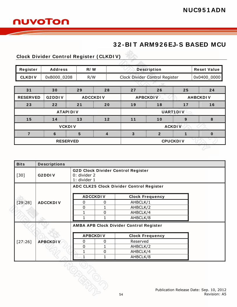
NUC951ADN
32-BIT ARM926EJ-S BASED MCU
Publication Release Date: Sep. 10, 2012 Revision: A5 54
Clock Divider Control Register (CLKDIV)
Register Address R/W Description Reset Value
CLKDIV 0xB000_0208 R/W Clock Divider Control Register 0x0400_0000
31 30 29 28 27 26 25 24
RESERVED G2DDIV ADCCKDIV APBCKDIV AHBCKDIV 23 22 21 20 19 18 17 16
ATAPIDIV UART1DIV 15 14 13 12 11 10 9 8
VCKDIV ACKDIV 7 6 5 4 3 2 1 0
RESERVED CPUCKDIV
Bits Descriptions
[30] G2DDIV G2D Clock Divider Control Register 0: divider 2 1: divider 1
[29:28] ADCCKDIV
ADC CLK25 Clock Divider Control Register
ADCCKDIV Clock Frequency 0 0 AHBCLK/1 0 1 AHBCLK/2 1 0 AHBCLK/4 1 1 AHBCLK/8
[27:26] APBCKDIV
AMBA APB Clock Divider Control Register
APBCKDIV Clock Frequency 0 0 Reserved 0 1 AHBCLK/2 1 0 AHBCLK/4 1 1 AHBCLK/8

NUC951ADN
32-BIT ARM926EJ-S BASED MCU
Publication Release Date: Sep. 10, 2012 Revision: A5 55
[25:24] AHBCKDIV
AMBA AHB Clock (AHBCLK) Divider Control Register
AHBCKDIV Clock Frequency 0 0 CPUCLK/1 0 1 CPUCLK/2 1 0 CPUCLK/4 1 1 CPUCLK/8
[23:20] ATAPIDIV
ATAPI Engine Clock Source Divider Control Register ATAPICK = ATAPI clock/(ATAPIDIV +1) Where (1) ATAPIDIV is 0~15 (2) ATAPI clock is the clock source output by ATAPISEL control reg.
[19:16] UART1DIV
UART1 Clock Source Divider Control Register UART1CK = UART1 clock/(UART1DIV +1) Where (1) UART1DIV is 0~15 (2) UART1 clock is the clock source output by UART1SEL control reg.
[15:12] VCKDIV
LCD Clock Source Divider Control Register LCD_CLK = VCK clock/(VCKDIV +1) Where (1) VCKDIV is 0~15 (2) VCK clock is the clock source output by VCKSEL control register
[11:8] ACKDIV
Audio Clock Source Divider Control Register Audio_CLK = ACK clock/(ACKDIV +1) Where (1) ACKDIV is 0~15 (2) ACK clock is the clock source output by ACKSEL control register
[3:0] CPUCKDIV
CPU Clock Source Divider Control Register CPUCLK = CCK clock/(CPUCKDIV +1) Where (1) CPUCKDIV is 0~15 (2) CCK clock is the clock source output by CPUCKSEL control register
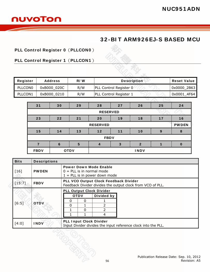
NUC951ADN
32-BIT ARM926EJ-S BASED MCU
Publication Release Date: Sep. 10, 2012 Revision: A5 56
PLL Control Register 0(PLLCON0)
PLL Control Register 1(PLLCON1)
Register Address R/W Description Reset Value
PLLCON0 0xB000_020C R/W PLL Control Register 0 0x0000_2B63
PLLCON1 0xB000_0210 R/W PLL Control Register 1 0x0001_4F64
31 30 29 28 27 26 25 24
RESERVED
23 22 21 20 19 18 17 16
RESERVED PWDEN
15 14 13 12 11 10 9 8
FBDV
7 6 5 4 3 2 1 0
FBDV OTDV INDV Bits Descriptions
[16] PWDEN Power Down Mode Enable 0 = PLL is in normal mode 1 = PLL is in power down mode
[15:7] FBDV PLL VCO Output Clock Feedback Divider Feedback Divider divides the output clock from VCO of PLL.
[6:5] OTDV
PLL Output Clock Divider OTDV Divided by
0 0 1 0 1 2 1 0 2 1 1 4
[4:0] INDV PLL Input Clock Divider Input Divider divides the input reference clock into the PLL.
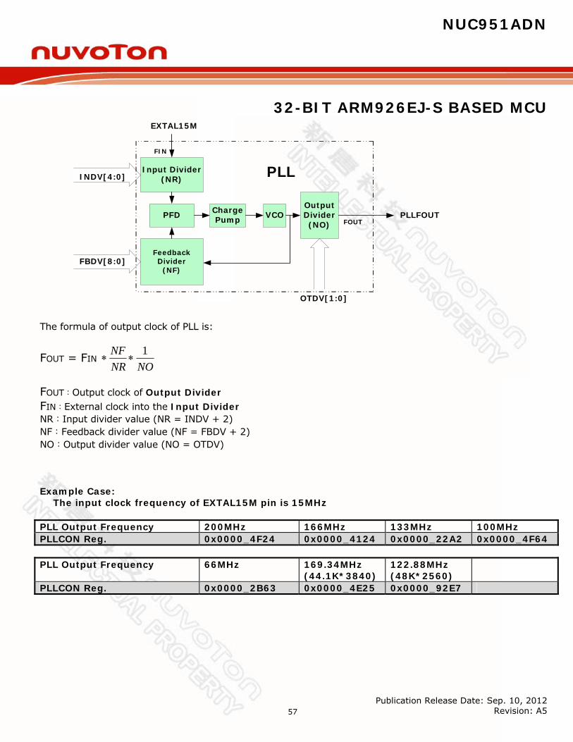
NUC951ADN
32-BIT ARM926EJ-S BASED MCU
Publication Release Date: Sep. 10, 2012 Revision: A5 57
Input Divider(NR)
PFD
Feedback Divider
(NF)
ChargePump VCO
Output Divider(NO)
EXTAL15M
OTDV[1:0]
PLL
PLLFOUT
INDV[4:0]
FBDV[8:0]
FIN
FOUT
The formula of output clock of PLL is:
FOUT = FIN NONR
NF 1
FOUT:Output clock of Output Divider FIN:External clock into the Input Divider NR:Input divider value (NR = INDV + 2) NF:Feedback divider value (NF = FBDV + 2) NO:Output divider value (NO = OTDV) Example Case:
The input clock frequency of EXTAL15M pin is 15MHz
PLL Output Frequency 200MHz 166MHz 133MHz 100MHz PLLCON Reg. 0x0000_4F24 0x0000_4124 0x0000_22A2 0x0000_4F64 PLL Output Frequency 66MHz 169.34MHz
(44.1K*3840) 122.88MHz (48K*2560)
PLLCON Reg. 0x0000_2B63 0x0000_4E25 0x0000_92E7
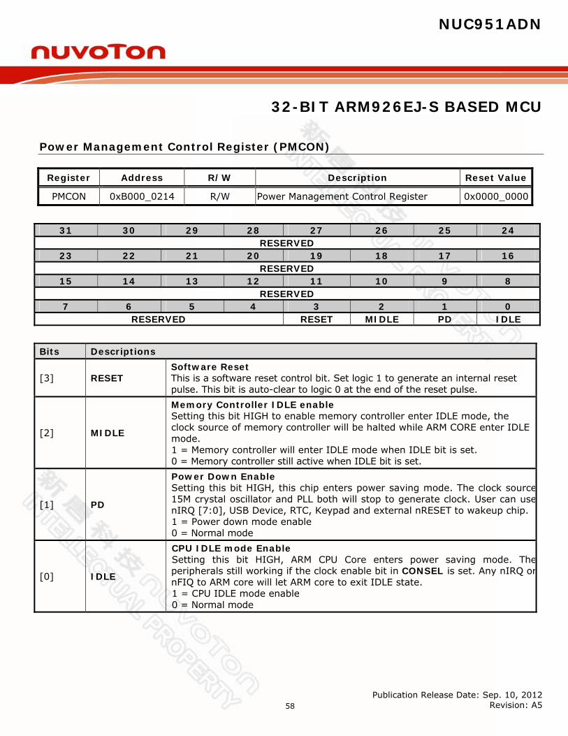
NUC951ADN
32-BIT ARM926EJ-S BASED MCU
Publication Release Date: Sep. 10, 2012 Revision: A5 58
Power Management Control Register (PMCON)
Register Address R/W Description Reset Value
PMCON 0xB000_0214 R/W Power Management Control Register 0x0000_0000
31 30 29 28 27 26 25 24
RESERVED 23 22 21 20 19 18 17 16
RESERVED 15 14 13 12 11 10 9 8
RESERVED 7 6 5 4 3 2 1 0
RESERVED RESET MIDLE PD IDLE
Bits Descriptions
[3] RESET Software Reset This is a software reset control bit. Set logic 1 to generate an internal reset pulse. This bit is auto-clear to logic 0 at the end of the reset pulse.
[2] MIDLE
Memory Controller IDLE enable Setting this bit HIGH to enable memory controller enter IDLE mode, the clock source of memory controller will be halted while ARM CORE enter IDLE mode. 1 = Memory controller will enter IDLE mode when IDLE bit is set. 0 = Memory controller still active when IDLE bit is set.
[1] PD
Power Down Enable Setting this bit HIGH, this chip enters power saving mode. The clock source15M crystal oscillator and PLL both will stop to generate clock. User can usenIRQ [7:0], USB Device, RTC, Keypad and external nRESET to wakeup chip. 1 = Power down mode enable 0 = Normal mode
[0] IDLE
CPU IDLE mode Enable Setting this bit HIGH, ARM CPU Core enters power saving mode. Theperipherals still working if the clock enable bit in CONSEL is set. Any nIRQ ornFIQ to ARM core will let ARM core to exit IDLE state. 1 = CPU IDLE mode enable 0 = Normal mode
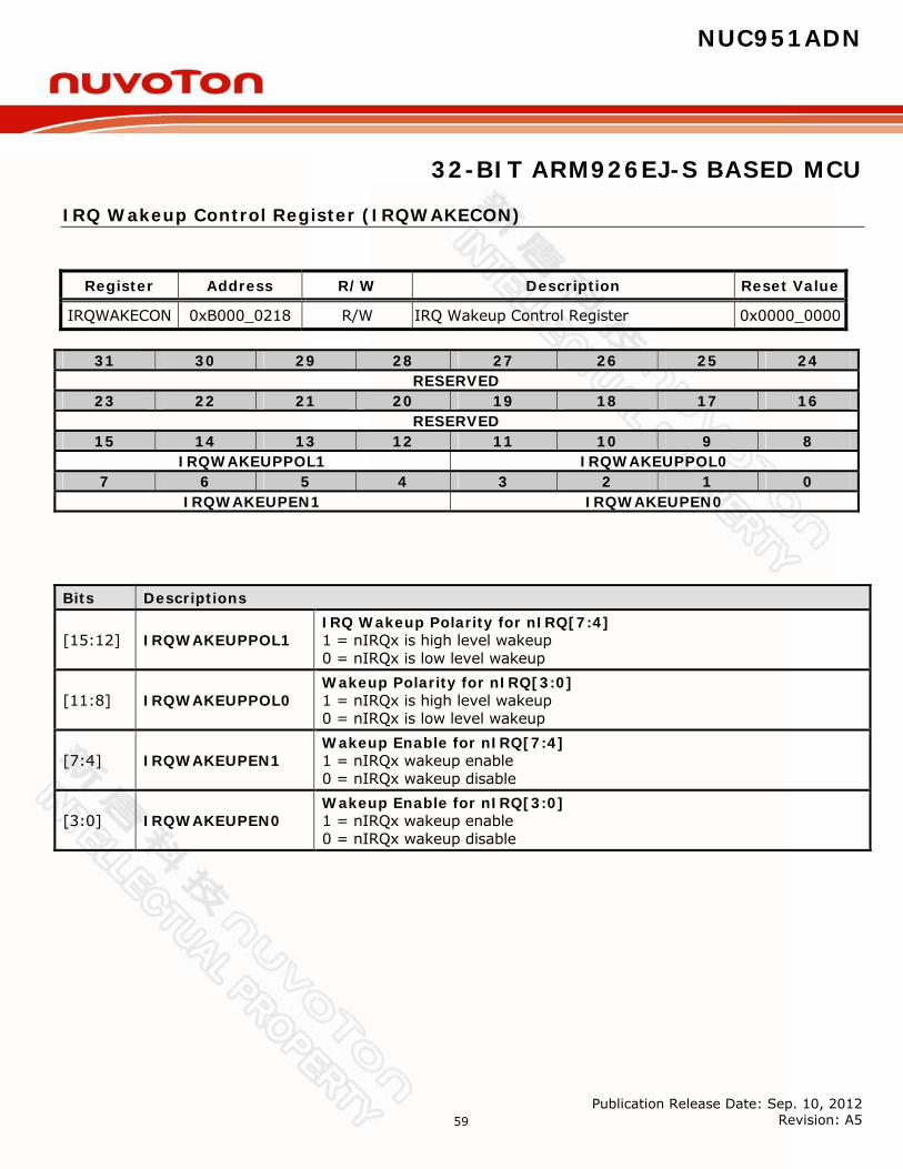
NUC951ADN
32-BIT ARM926EJ-S BASED MCU
Publication Release Date: Sep. 10, 2012 Revision: A5 59
IRQ Wakeup Control Register (IRQWAKECON)
Register Address R/W Description Reset Value
IRQWAKECON 0xB000_0218 R/W IRQ Wakeup Control Register 0x0000_0000
31 30 29 28 27 26 25 24 RESERVED
23 22 21 20 19 18 17 16 RESERVED
15 14 13 12 11 10 9 8 IRQWAKEUPPOL1 IRQWAKEUPPOL0
7 6 5 4 3 2 1 0 IRQWAKEUPEN1 IRQWAKEUPEN0
Bits Descriptions
[15:12] IRQWAKEUPPOL1 IRQ Wakeup Polarity for nIRQ[7:4] 1 = nIRQx is high level wakeup 0 = nIRQx is low level wakeup
[11:8] IRQWAKEUPPOL0 Wakeup Polarity for nIRQ[3:0] 1 = nIRQx is high level wakeup 0 = nIRQx is low level wakeup
[7:4] IRQWAKEUPEN1 Wakeup Enable for nIRQ[7:4] 1 = nIRQx wakeup enable 0 = nIRQx wakeup disable
[3:0] IRQWAKEUPEN0 Wakeup Enable for nIRQ[3:0] 1 = nIRQx wakeup enable 0 = nIRQx wakeup disable
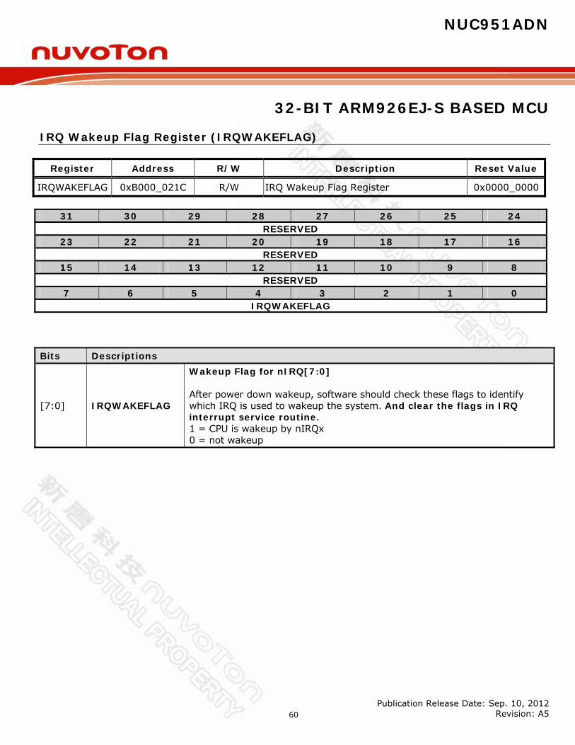
NUC951ADN
32-BIT ARM926EJ-S BASED MCU
Publication Release Date: Sep. 10, 2012 Revision: A5 60
IRQ Wakeup Flag Register (IRQWAKEFLAG)
Register Address R/W Description Reset Value
IRQWAKEFLAG 0xB000_021C R/W IRQ Wakeup Flag Register 0x0000_0000
31 30 29 28 27 26 25 24 RESERVED
23 22 21 20 19 18 17 16 RESERVED
15 14 13 12 11 10 9 8 RESERVED
7 6 5 4 3 2 1 0 IRQWAKEFLAG
Bits Descriptions
[7:0] IRQWAKEFLAG
Wakeup Flag for nIRQ[7:0] After power down wakeup, software should check these flags to identify which IRQ is used to wakeup the system. And clear the flags in IRQ interrupt service routine. 1 = CPU is wakeup by nIRQx 0 = not wakeup
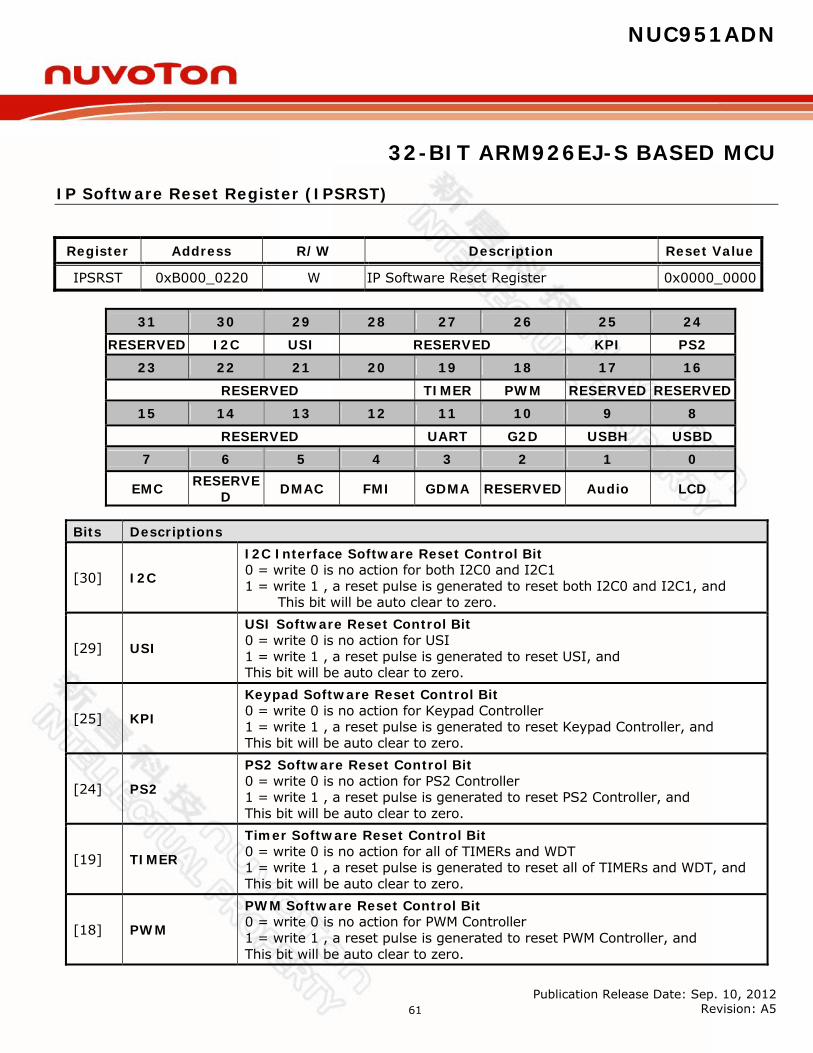
NUC951ADN
32-BIT ARM926EJ-S BASED MCU
Publication Release Date: Sep. 10, 2012 Revision: A5 61
IP Software Reset Register (IPSRST)
Register Address R/W Description Reset Value
IPSRST 0xB000_0220 W IP Software Reset Register 0x0000_0000
31 30 29 28 27 26 25 24
RESERVED I2C USI RESERVED KPI PS2
23 22 21 20 19 18 17 16
RESERVED TIMER PWM RESERVED RESERVED
15 14 13 12 11 10 9 8
RESERVED UART G2D USBH USBD
7 6 5 4 3 2 1 0
EMC RESERVED DMAC FMI GDMA RESERVED Audio LCD
Bits Descriptions
[30] I2C
I2C Interface Software Reset Control Bit 0 = write 0 is no action for both I2C0 and I2C1 1 = write 1 , a reset pulse is generated to reset both I2C0 and I2C1, and
This bit will be auto clear to zero.
[29] USI
USI Software Reset Control Bit 0 = write 0 is no action for USI 1 = write 1 , a reset pulse is generated to reset USI, and This bit will be auto clear to zero.
[25] KPI
Keypad Software Reset Control Bit 0 = write 0 is no action for Keypad Controller 1 = write 1 , a reset pulse is generated to reset Keypad Controller, and This bit will be auto clear to zero.
[24] PS2
PS2 Software Reset Control Bit 0 = write 0 is no action for PS2 Controller 1 = write 1 , a reset pulse is generated to reset PS2 Controller, and This bit will be auto clear to zero.
[19] TIMER
Timer Software Reset Control Bit 0 = write 0 is no action for all of TIMERs and WDT 1 = write 1 , a reset pulse is generated to reset all of TIMERs and WDT, and This bit will be auto clear to zero.
[18] PWM
PWM Software Reset Control Bit 0 = write 0 is no action for PWM Controller 1 = write 1 , a reset pulse is generated to reset PWM Controller, and This bit will be auto clear to zero.

NUC951ADN
32-BIT ARM926EJ-S BASED MCU
Publication Release Date: Sep. 10, 2012 Revision: A5 62
[11] UART
UART Software Reset Control Bit 0 = write 0 is no action for all of UARTs 1 = write 1 , a reset pulse is generated to reset all of UARTs, and This bit will be auto clear to zero.
[10] G2D
2D Graphic Controller Software Reset Control Bit 0 = write 0 is no action for 2D graphic Controller 1 = write 1 , a reset pulse is generated to reset 2D Graphic Controller, and This bit will be auto clear to zero.
[9] USBH
USB Software Reset Control Bit 0 = write 0 is no action for USB Host Controller 1 = write 1 , a reset pulse is generated to reset USB Host Controller, and This bit will be auto clear to zero.
[8] USBD
USB Device Software Reset Control Bit 0 = write 0 is no action for USB Device Controller 1 = write 1 , a reset pulse is generated to reset USB Device Controller, and This bit will be auto clear to zero.
[7] EMC
EMC Software Reset Control Bit 0 = write 0 is no action for EMC Controller 1 = write 1 , a reset pulse is generated to reset EMC Controller, and This bit will be auto clear to zero.
[5] DMAC
DMAC Software Reset Control Bit 0 = write 0 is no action for DMA Controller 1 = write 1 , a reset pulse is generated to reset DMA Controller, and This bit will be auto clear to zero.
[4] FMI
FMI Software Reset Control Bit 0 = write 0 is no action for FMI Controller 1 = write 1 , a reset pulse is generated to reset FMI Controller, and This bit will be auto clear to zero.
[3] GDMA
GDMA Software Reset Control Bit 0 = write 0 is no action for GDMA Controller 1 = write 1 , a reset pulse is generated to reset GDMA Controller, and This bit will be auto clear to zero.
[1] Audio
Audio Controller Software Reset Control Bit 0 = write 0 is no action for Audio Controller 1 = write 1 , a reset pulse is generated to reset Audio Controller, and This bit will be auto clear to zero.
[0] LCD
LCD Controller Software Reset Control Bit 0 = write 0 is no action for LCD Controller 1 = write 1 , a reset pulse is generated to reset LCD Controller, and This bit will be auto clear to zero.
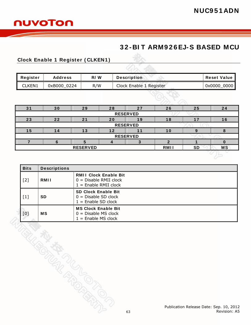
NUC951ADN
32-BIT ARM926EJ-S BASED MCU
Publication Release Date: Sep. 10, 2012 Revision: A5 63
Clock Enable 1 Register (CLKEN1)
Register Address R/W Description Reset Value
CLKEN1 0xB000_0224 R/W Clock Enable 1 Register 0x0000_0000
31 30 29 28 27 26 25 24 RESERVED
23 22 21 20 19 18 17 16 RESERVED
15 14 13 12 11 10 9 8 RESERVED
7 6 5 4 3 2 1 0 RESERVED RMII SD MS
Bits Descriptions
[2] RMII RMII Clock Enable Bit 0 = Disable RMII clock 1 = Enable RMII clock
[1] SD SD Clock Enable Bit 0 = Disable SD clock 1 = Enable SD clock
[0] MS MS Clock Enable Bit 0 = Disable MS clock 1 = Enable MS clock

NUC951ADN
32-BIT ARM926EJ-S BASED MCU
Publication Release Date: Sep. 10, 2012 Revision: A5 64
Clock Divider Control 1 Register (CLKDIV1)
Register Address R/W Description Reset Value
CLKDIV1 0xB000_0228 R/W Clock Divider Control 1 Register 0x0000_0000
31 30 29 28 27 26 25 24 RESERVED
23 22 21 20 19 18 17 16 RESERVED
15 14 13 12 11 10 9 8 SD_DIV
7 6 5 4 3 2 1 0 MS_DIV
Bits Descriptions
[15:8] SD_DIV SD divider SD_CLK = Source Clock/(SD_DIV +1) Where Source Clock selection is controlled by MSDSEL of register CLKSEL.
[7:0] MS_DIV MS divider MS_CLK = Source Clock/(MS_DIV +1) Where Source Clock selection is controlled by MSDSEL of register CLKSEL.

NUC951ADN
32-BIT ARM926EJ-S BASED MCU
Publication Release Date: Sep. 10, 2012 Revision: A5 65
7.4 External Bus Interface
7.4.1 Overview This chip supports External Bus Interface (EBI), which controls the access to the external memory (ROM/FLASH, SDRAM) and External I/O devices. The EBI has chip select signals to select one ROM/FLASH bank, two SDRAM banks, and five External I/O banks with 25-bit address bus. It supports 8-bit, 16-bit or 32-bit external data bus width for each bank. The EBI has the following functions: SDRAM controller EBI control register ROM/FLASH interface External I/O interface
7.4.2 Functional Description 7.4.2.1 SDRAM Controller The SDRAM controller module contains configuration registers, timing control registers, common control register and other logic to provide 8,16 or 32 bits SDRAM interface with a single 8,16 or 32 bits SDRAM device or two 8-bit devices wired to give a 16-bit data path or two 16-bit devices wired to give a 32-bit data path. The SDRAM controller has the following features: Supports up to 2 external SDRAM devices Maximum size of each device is 128M bytes 8,16 or 32-bit data interface Programmable CAS Latency: 1,2 and 3 Fixed Burst Length: 1 Sequential burst type Write Burst Length mode is Burst Auto Refresh Mode and Self Refresh Mode Adjustable Refresh Rate Power up sequence
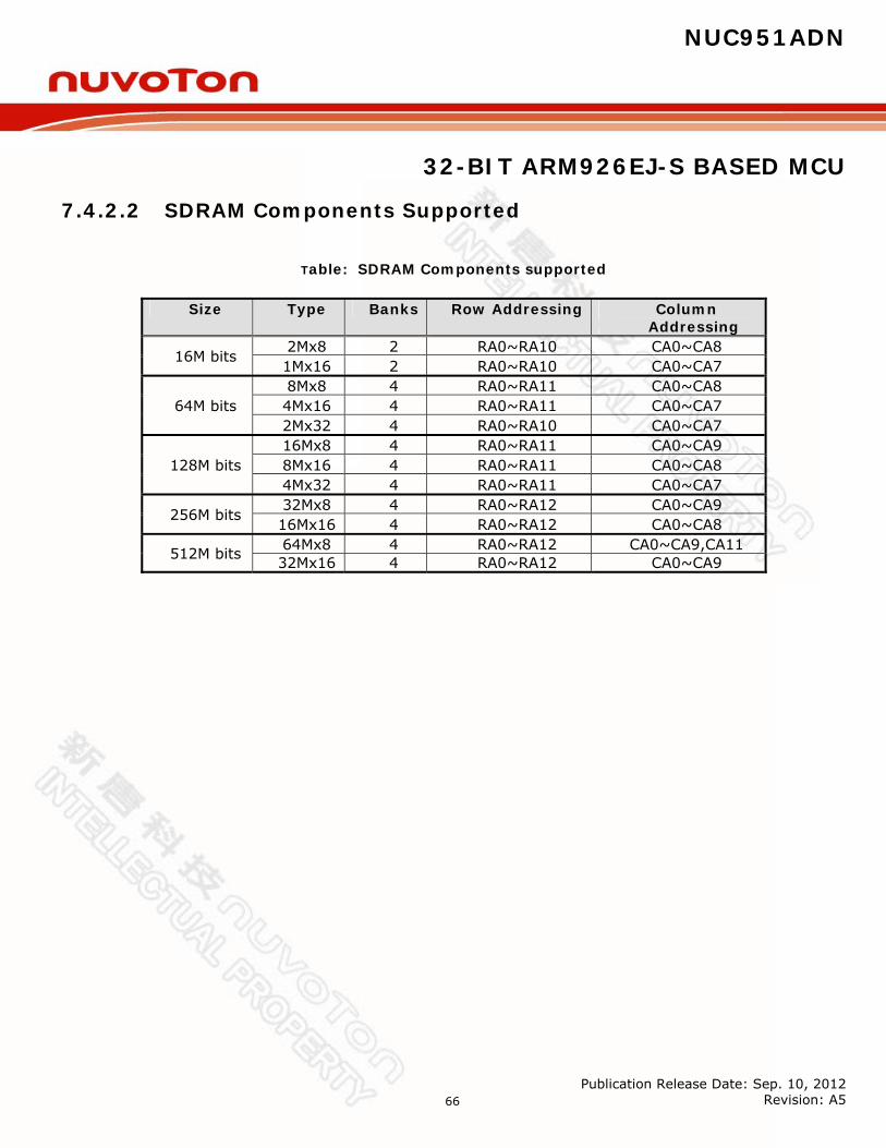
NUC951ADN
32-BIT ARM926EJ-S BASED MCU
Publication Release Date: Sep. 10, 2012 Revision: A5 66
7.4.2.2 SDRAM Components Supported
Table: SDRAM Components supported
Size Type Banks Row Addressing Column Addressing
16M bits 2Mx8 2 RA0~RA10 CA0~CA8 1Mx16 2 RA0~RA10 CA0~CA7
64M bits 8Mx8 4 RA0~RA11 CA0~CA8 4Mx16 4 RA0~RA11 CA0~CA7 2Mx32 4 RA0~RA10 CA0~CA7
128M bits 16Mx8 4 RA0~RA11 CA0~CA9 8Mx16 4 RA0~RA11 CA0~CA8 4Mx32 4 RA0~RA11 CA0~CA7
256M bits 32Mx8 4 RA0~RA12 CA0~CA9 16Mx16 4 RA0~RA12 CA0~CA8
512M bits 64Mx8 4 RA0~RA12 CA0~CA9,CA11 32Mx16 4 RA0~RA12 CA0~CA9
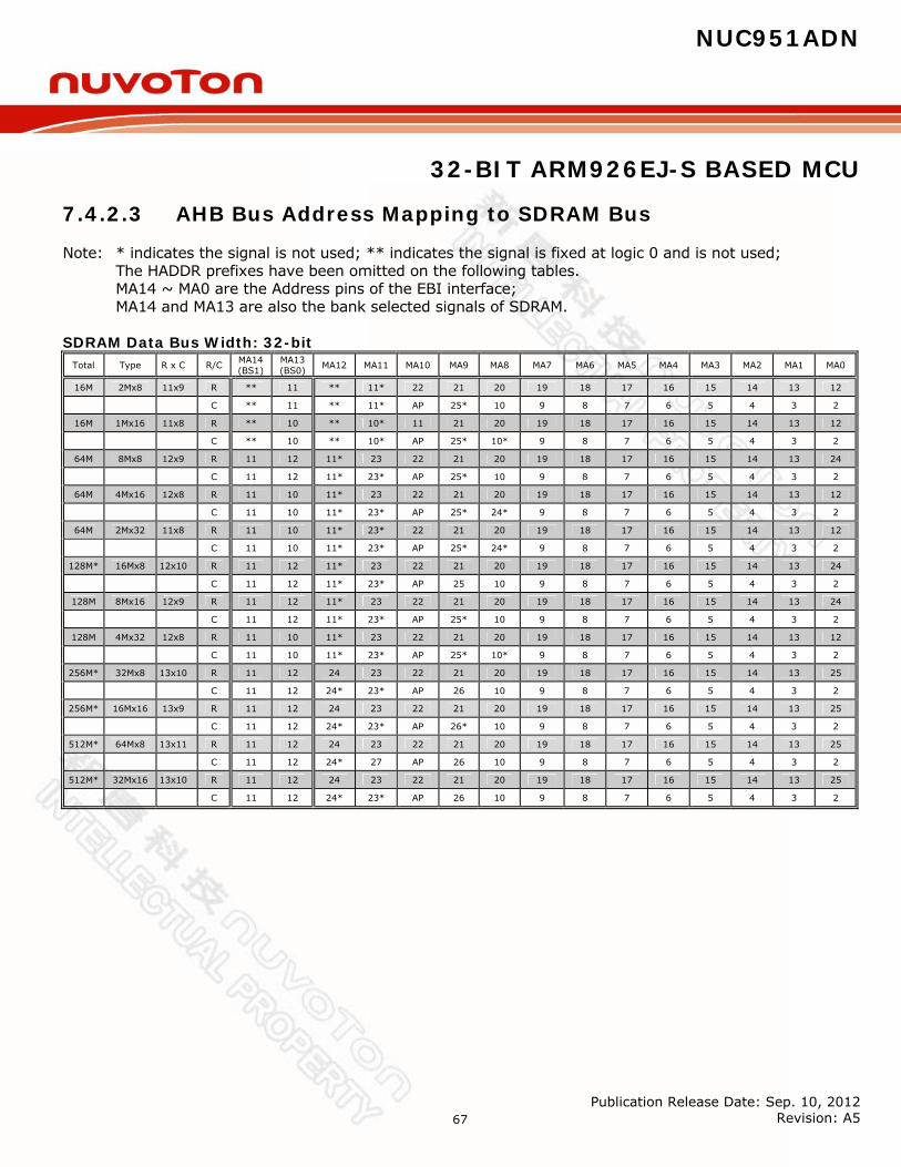
NUC951ADN
32-BIT ARM926EJ-S BASED MCU
Publication Release Date: Sep. 10, 2012 Revision: A5 67
7.4.2.3 AHB Bus Address Mapping to SDRAM Bus Note: * indicates the signal is not used; ** indicates the signal is fixed at logic 0 and is not used;
The HADDR prefixes have been omitted on the following tables. MA14 ~ MA0 are the Address pins of the EBI interface; MA14 and MA13 are also the bank selected signals of SDRAM.
SDRAM Data Bus Width: 32-bit Total Type R x C R/C MA14
(BS1) MA13 (BS0) MA12 MA11 MA10 MA9 MA8 MA7 MA6 MA5 MA4 MA3 MA2 MA1 MA0
16M 2Mx8 11x9 R ** 11 ** 11* 22 21 20 19 18 17 16 15 14 13 12
C ** 11 ** 11* AP 25* 10 9 8 7 6 5 4 3 2
16M 1Mx16 11x8 R ** 10 ** 10* 11 21 20 19 18 17 16 15 14 13 12
C ** 10 ** 10* AP 25* 10* 9 8 7 6 5 4 3 2
64M 8Mx8 12x9 R 11 12 11* 23 22 21 20 19 18 17 16 15 14 13 24
C 11 12 11* 23* AP 25* 10 9 8 7 6 5 4 3 2
64M 4Mx16 12x8 R 11 10 11* 23 22 21 20 19 18 17 16 15 14 13 12
C 11 10 11* 23* AP 25* 24* 9 8 7 6 5 4 3 2
64M 2Mx32 11x8 R 11 10 11* 23* 22 21 20 19 18 17 16 15 14 13 12
C 11 10 11* 23* AP 25* 24* 9 8 7 6 5 4 3 2
128M* 16Mx8 12x10 R 11 12 11* 23 22 21 20 19 18 17 16 15 14 13 24
C 11 12 11* 23* AP 25 10 9 8 7 6 5 4 3 2
128M 8Mx16 12x9 R 11 12 11* 23 22 21 20 19 18 17 16 15 14 13 24
C 11 12 11* 23* AP 25* 10 9 8 7 6 5 4 3 2
128M 4Mx32 12x8 R 11 10 11* 23 22 21 20 19 18 17 16 15 14 13 12
C 11 10 11* 23* AP 25* 10* 9 8 7 6 5 4 3 2
256M* 32Mx8 13x10 R 11 12 24 23 22 21 20 19 18 17 16 15 14 13 25
C 11 12 24* 23* AP 26 10 9 8 7 6 5 4 3 2
256M* 16Mx16 13x9 R 11 12 24 23 22 21 20 19 18 17 16 15 14 13 25
C 11 12 24* 23* AP 26* 10 9 8 7 6 5 4 3 2
512M* 64Mx8 13x11 R 11 12 24 23 22 21 20 19 18 17 16 15 14 13 25
C 11 12 24* 27 AP 26 10 9 8 7 6 5 4 3 2
512M* 32Mx16 13x10 R 11 12 24 23 22 21 20 19 18 17 16 15 14 13 25
C 11 12 24* 23* AP 26 10 9 8 7 6 5 4 3 2

NUC951ADN
32-BIT ARM926EJ-S BASED MCU
Publication Release Date: Sep. 10, 2012 Revision: A5 68
SDRAM Data Bus Width: 16-bit Total Type R x C R/
C MA14 (BS1)
MA13 (BS0) MA12 MA11 MA10 MA9 MA8 MA7 MA6 MA5 MA4 MA3 MA2 MA1 MA0
16M 2Mx8 11x9 R ** 10 ** 10* 21 20 19 18 17 16 15 14 13 12 11
C ** 10 ** 10* AP 24* 9 8 7 6 5 4 3 2 1
16M 1Mx16 11x8 R ** 9 ** 9* 10 20 19 18 17 16 15 14 13 12 11
C ** 9 ** 9* AP 24* 9* 8 7 6 5 4 3 2 1
64M 8Mx8 12x9 R 10 11 10* 22 21 20 19 18 17 16 15 14 13 12 23
C 10 11 10* 22* AP 24* 9 8 7 6 5 4 3 2 1
64M 4Mx16 12x8 R 10 9 10* 22 21 20 19 18 17 16 15 14 13 12 11
C 10 9 10* 22* AP 24* 23* 8 7 6 5 4 3 2 1
64M 2Mx32 11x8 R 10 9 10* 22* 21 20 19 18 17 16 15 14 13 12 11
C 10 9 10* 22* AP 24* 23* 8 7 6 5 4 3 2 1
128M 16Mx8 12x10 R 10 11 10* 22 21 20 19 18 17 16 15 14 13 12 23
C 10 11 10* 22* AP 24 9 8 7 6 5 4 3 2 1
128M 8Mx16 12x9 R 10 11 10* 22 21 20 19 18 17 16 15 14 13 12 23
C 10 11 10* 22* AP 24* 9 8 7 6 5 4 3 2 1
128M 4Mx32 12x8 R 10 9 10* 22 21 20 19 18 17 16 15 14 13 12 11
C 10 9 10* 22* AP 24* 9* 8 7 6 5 4 3 2 1
256M* 32Mx8 13x10 R 10 11 23 22 21 20 19 18 17 16 15 14 13 12 24
C 10 11 23* 22* AP 25 9 8 7 6 5 4 3 2 1
256M 16Mx16 13x9 R 10 11 23 22 21 20 19 18 17 16 15 14 13 12 24
C 10 11 23* 22* AP 25* 9 8 7 6 5 4 3 2 1
512M 64Mx8 13x11 R 10 11 23 22 21 20 19 18 17 16 15 14 13 12 24
C 10 11 23* 26 AP 25 9 8 7 6 5 4 3 2 1
512M 32Mx16 13x10 R 10 11 23 22 21 20 19 18 17 16 15 14 13 12 24
C 10 11 23* 22* AP 25 9 8 7 6 5 4 3 2 1

NUC951ADN
32-BIT ARM926EJ-S BASED MCU
Publication Release Date: Sep. 10, 2012 Revision: A5 69
SDRAM Data Bus Width: 8-bit
Total Type R x C R/C MA14 (BS1)
MA13 (BS0) MA12 MA11 MA10 MA9 MA8 MA7 MA6 MA5 MA4 MA3 MA2 MA1 MA0
16M 2Mx8 11x9 R ** 9 ** 9* 20 19 18 17 16 15 14 13 12 11 10
C ** 9 ** 9* AP 23* 8 7 6 5 4 3 2 1 0
16M 1Mx16 11x8 R ** 8 ** 8* 9 19 18 17 16 15 14 13 12 11 10
C ** 8 ** 8* AP 23* 8* 7 6 5 4 3 2 1 0
64M 8Mx8 12x9 R 9 10 9* 21 20 19 18 17 16 15 14 13 12 11 22
C 9 10 9* 21* AP 23* 8 7 6 5 4 3 2 1 1
64M 4Mx16 12x8 R 9 8 9* 21 20 19 18 17 16 15 14 13 12 11 10
C 9 8 9* 21* AP 23* 22* 7 6 5 4 3 2 1 0
64M 2Mx32 11x8 R 9 8 9* 21* 20 19 18 17 16 15 14 13 12 11 10
C 9 8 9* 21* AP 23* 22* 7 6 5 4 3 2 1 0
128M 16Mx8 12x10 R 9 10 9* 21 20 19 18 17 16 15 14 13 12 11 22
C 9 10 9* 21* AP 23 8 7 6 5 4 3 2 1 0
128M 8Mx16 12x9 R 9 10 9* 21 20 19 18 17 16 15 14 13 12 11 22
C 9 10 9* 21* AP 23* 8 7 6 5 4 3 2 1 0
128M 4Mx32 12x8 R 9 8 9* 21 20 19 18 17 16 15 14 13 12 11 10
C 9 8 9* 21* AP 23* 8* 7 6 5 4 3 2 1 0
256M 32Mx8 13x10 R 9 10 22 21 20 19 18 17 16 15 14 13 12 11 23
C 9 10 22* 21* AP 24 8 7 6 5 4 3 2 1 0
256M 16Mx16 13x9 R 9 10 22 21 20 19 18 17 16 15 14 13 12 11 23
C 9 10 22* 21* AP 24* 8 7 6 5 4 3 2 1 0
512M 64Mx8 13x11 R 9 10 22 21 20 19 18 17 16 15 14 13 12 11 23
C 9 10 22* 25 AP 24 8 7 6 5 4 3 2 1 0
512M 32Mx16 13x10 R 9 10 22 21 20 19 18 17 16 15 14 13 12 11 23
C 9 10 22* 21* AP 24 8 7 6 5 4 3 2 1 0
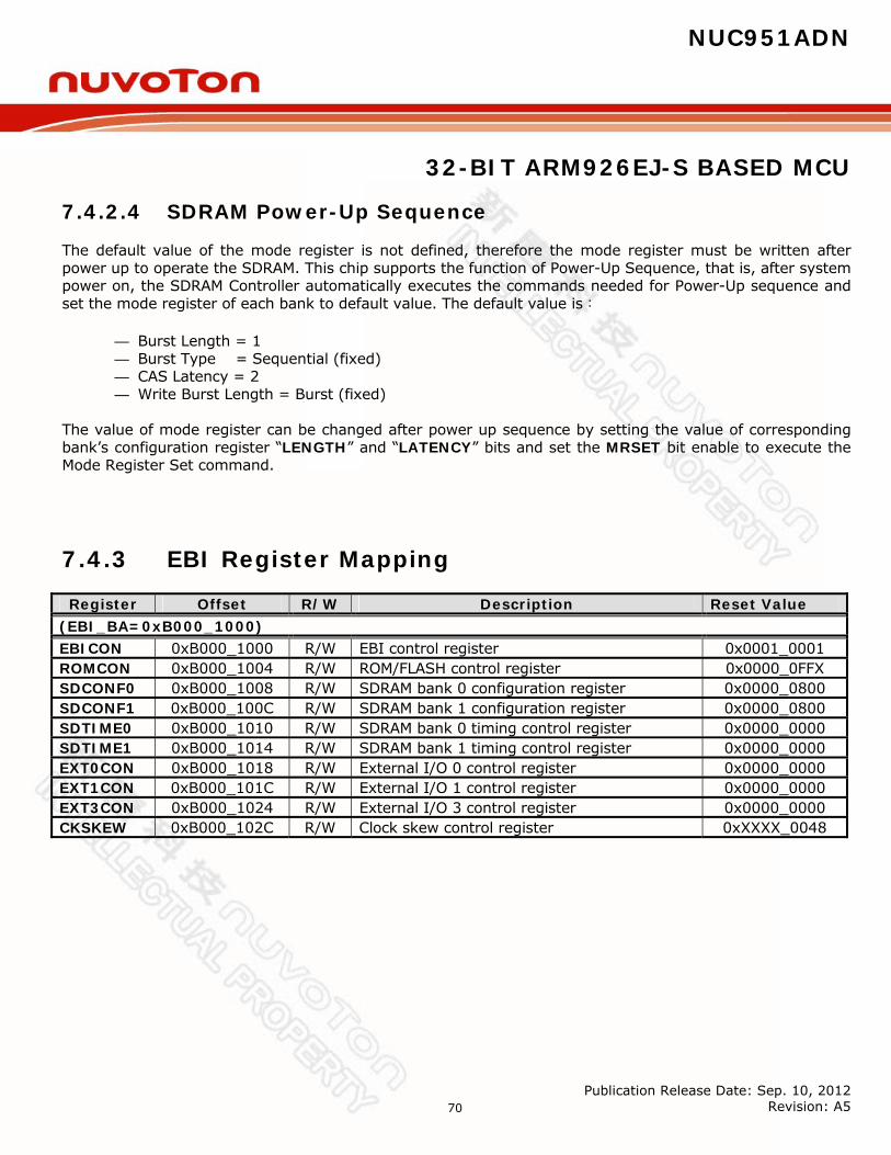
NUC951ADN
32-BIT ARM926EJ-S BASED MCU
Publication Release Date: Sep. 10, 2012 Revision: A5 70
7.4.2.4 SDRAM Power-Up Sequence The default value of the mode register is not defined, therefore the mode register must be written after power up to operate the SDRAM. This chip supports the function of Power-Up Sequence, that is, after system power on, the SDRAM Controller automatically executes the commands needed for Power-Up sequence and set the mode register of each bank to default value. The default value is:
— Burst Length = 1 — Burst Type = Sequential (fixed) — CAS Latency = 2 — Write Burst Length = Burst (fixed)
The value of mode register can be changed after power up sequence by setting the value of corresponding bank’s configuration register “LENGTH” and “LATENCY” bits and set the MRSET bit enable to execute the Mode Register Set command.
7.4.3 EBI Register Mapping
Register Offset R/W Description Reset Value (EBI_BA=0xB000_1000) EBICON 0xB000_1000 R/W EBI control register 0x0001_0001 ROMCON 0xB000_1004 R/W ROM/FLASH control register 0x0000_0FFX SDCONF0 0xB000_1008 R/W SDRAM bank 0 configuration register 0x0000_0800 SDCONF1 0xB000_100C R/W SDRAM bank 1 configuration register 0x0000_0800 SDTIME0 0xB000_1010 R/W SDRAM bank 0 timing control register 0x0000_0000 SDTIME1 0xB000_1014 R/W SDRAM bank 1 timing control register 0x0000_0000 EXT0CON 0xB000_1018 R/W External I/O 0 control register 0x0000_0000 EXT1CON 0xB000_101C R/W External I/O 1 control register 0x0000_0000 EXT3CON 0xB000_1024 R/W External I/O 3 control register 0x0000_0000 CKSKEW 0xB000_102C R/W Clock skew control register 0xXXXX_0048
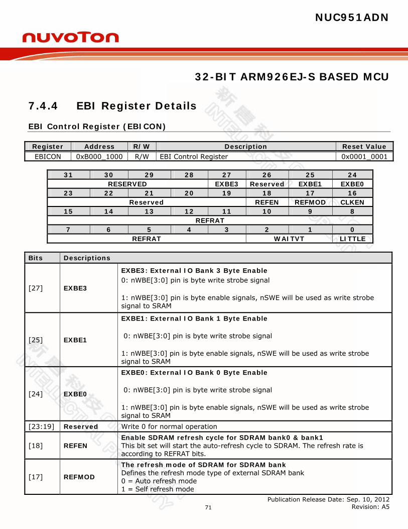
NUC951ADN
32-BIT ARM926EJ-S BASED MCU
Publication Release Date: Sep. 10, 2012 Revision: A5 71
7.4.4 EBI Register Details
EBI Control Register (EBICON)
Register Address R/W Description Reset Value EBICON 0xB000_1000 R/W EBI Control Register 0x0001_0001
31 30 29 28 27 26 25 24
RESERVED EXBE3 Reserved EXBE1 EXBE0 23 22 21 20 19 18 17 16
Reserved REFEN REFMOD CLKEN 15 14 13 12 11 10 9 8
REFRAT 7 6 5 4 3 2 1 0
REFRAT WAITVT LITTLE Bits Descriptions
[27] EXBE3
EXBE3: External IO Bank 3 Byte Enable 0: nWBE[3:0] pin is byte write strobe signal
1: nWBE[3:0] pin is byte enable signals, nSWE will be used as write strobe signal to SRAM
[25] EXBE1
EXBE1: External IO Bank 1 Byte Enable
0: nWBE[3:0] pin is byte write strobe signal
1: nWBE[3:0] pin is byte enable signals, nSWE will be used as write strobe signal to SRAM
[24] EXBE0
EXBE0: External IO Bank 0 Byte Enable
0: nWBE[3:0] pin is byte write strobe signal
1: nWBE[3:0] pin is byte enable signals, nSWE will be used as write strobe signal to SRAM
[23:19] Reserved Write 0 for normal operation
[18] REFEN Enable SDRAM refresh cycle for SDRAM bank0 & bank1 This bit set will start the auto-refresh cycle to SDRAM. The refresh rate is according to REFRAT bits.
[17] REFMOD
The refresh mode of SDRAM for SDRAM bank Defines the refresh mode type of external SDRAM bank 0 = Auto refresh mode 1 = Self refresh mode
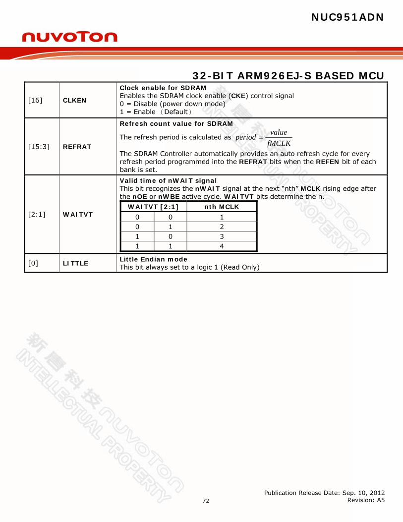
NUC951ADN
32-BIT ARM926EJ-S BASED MCU
Publication Release Date: Sep. 10, 2012 Revision: A5 72
[16] CLKEN
Clock enable for SDRAM Enables the SDRAM clock enable (CKE) control signal 0 = Disable (power down mode) 1 = Enable (Default)
[15:3] REFRAT
Refresh count value for SDRAM
The refresh period is calculated as fMCLK
valueperiod
The SDRAM Controller automatically provides an auto refresh cycle for every refresh period programmed into the REFRAT bits when the REFEN bit of each bank is set.
[2:1] WAITVT
Valid time of nWAIT signal This bit recognizes the nWAIT signal at the next “nth” MCLK rising edge after the nOE or nWBE active cycle. WAITVT bits determine the n.
WAITVT [2:1] nth MCLK 0 0 1 0 1 2 1 0 3 1 1 4
[0] LITTLE Little Endian mode This bit always set to a logic 1 (Read Only)

NUC951ADN
32-BIT ARM926EJ-S BASED MCU
Publication Release Date: Sep. 10, 2012 Revision: A5 73
ROM/Flash Control Register (ROMCON)
Register Address R/W Description Reset Value ROMCON 0xB000_1004 R/W ROM/FLASH Control Register 0x0000_0FFX
31 30 29 28 27 26 25 24
BASADDR 23 22 21 20 19 18 17 16
BASADDR SIZE 15 14 13 12 11 10 9 8
SIZE Reserved tPA 7 6 5 4 3 2 1 0
tACC BTSIZE PGMODE Bits Descriptions
[31:19] BASADDR
Base Address Pointer of ROM/Flash Bank The start address is calculated as ROM/Flash bank base pointer << 18. The base address pointer together with the “SIZE” bits constitutes the whole address range of each bank.
[18:15] SIZE
Size of ROM/FLASH Memory
SIZE [18:15] Byte 0 0 0 0 256K 0 0 1 0 512K 0 1 0 0 1M 0 1 1 0 2M 1 0 0 0 4M 1 0 1 0 8M 1 1 0 0 16M
Others Reserved Note: 16M byte is only for 32-bit data bus width
[11:8] tPA
Page Mode Access Cycle Time tPA[11:8] MCLK tPA[11:8] MCLK
0 0 0 0 1 1 0 0 0 10 0 0 0 1 2 1 0 0 1 12 0 0 1 0 3 1 0 1 0 14 0 0 1 1 4 1 0 1 1 16 0 1 0 0 5 1 1 0 0 18 0 1 0 1 6 1 1 0 1 20 0 1 1 0 7 1 1 1 0 22 0 1 1 1 8 1 1 1 1 24
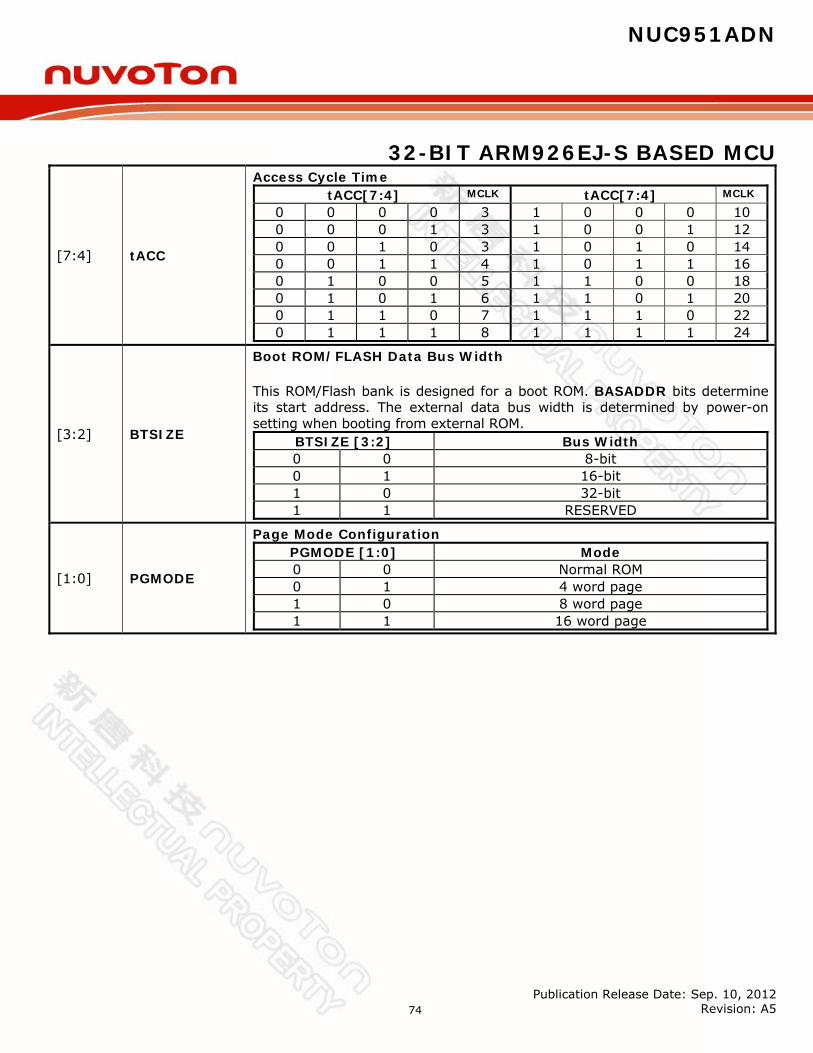
NUC951ADN
32-BIT ARM926EJ-S BASED MCU
Publication Release Date: Sep. 10, 2012 Revision: A5 74
[7:4] tACC
Access Cycle Time tACC[7:4] MCLK tACC[7:4] MCLK
0 0 0 0 3 1 0 0 0 10 0 0 0 1 3 1 0 0 1 12 0 0 1 0 3 1 0 1 0 14 0 0 1 1 4 1 0 1 1 16 0 1 0 0 5 1 1 0 0 18 0 1 0 1 6 1 1 0 1 20 0 1 1 0 7 1 1 1 0 22 0 1 1 1 8 1 1 1 1 24
[3:2] BTSIZE
Boot ROM/FLASH Data Bus Width
This ROM/Flash bank is designed for a boot ROM. BASADDR bits determine its start address. The external data bus width is determined by power-on setting when booting from external ROM.
BTSIZE [3:2] Bus Width 0 0 8-bit 0 1 16-bit 1 0 32-bit 1 1 RESERVED
[1:0] PGMODE
Page Mode Configuration PGMODE [1:0] Mode 0 0 Normal ROM 0 1 4 word page 1 0 8 word page 1 1 16 word page
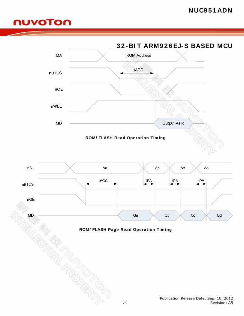
NUC951ADN
32-BIT ARM926EJ-S BASED MCU
Publication Release Date: Sep. 10, 2012 Revision: A5 75
ROM/FLASH Read Operation Timing
ROM/FLASH Page Read Operation Timing

NUC951ADN
32-BIT ARM926EJ-S BASED MCU
Publication Release Date: Sep. 10, 2012 Revision: A5 76
SDRAM Configuration Register (SDCONF0/1)
The configuration registers enable software to set a number of operating parameters for the SDRAM controller. There are two configuration registers SDCONF0 or SDCONF1 for SDRAM bank 0 or bank 1 respectively. Each bank can have a different configuration. Register Address R/W Description Reset Value SDCONF0 0xB000_1008 R/W SDRAM Bank 0 Configuration Register 0x0000_0800 SDCONF1 0xB000_100C R/W SDRAM Bank 1 Configuration Register 0x0000_0800
31 30 29 28 27 26 25 24
BASADDR 23 22 21 20 19 18 17 16
BASADDR RESERVED 15 14 13 12 11 10 9 8
MRSET RESERVED AUTOPR LATENCY RESERVED
7 6 5 4 3 2 1 0 COMPBK DBWD COLUMN SIZE
Bits Descriptions
[31:19] BASADDR
Base Address Pointer of SDRAM Bank 0/1 The start address is calculated as SDRAM bank 0/1 base pointer << 18. The SDRAM base address pointer together with the “SIZE” bits constitutes the whole address range of each SDRAM bank.
[15] MRSET SDRAM Mode Register Set Command for SDRAM Bank 0/1 This bit set will issue a mode register set command to SDRAM.
[13] AUTOPR
Auto Pre-charge Mode of SDRAM for SDRAM Bank 0/1 Enable the auto pre-charge function of external SDRAM bank 0/1 0 = Auto pre-charge 1 = No auto pre-charge
[12:11] LATENCY
The CAS Latency of SDRAM Bank 0/1 Defines the CAS latency of external SDRAM bank 0/1
LATENCY [12:11] MCLK 0 0 1 0 1 2 1 0 3 1 1 REVERSED
[7] COMPBK
Number of Component Bank in SDRAM Bank 0/1 Indicates the number of component bank (2 or 4 banks) in external SDRAM bank 0/1. 0 = 2 banks 1 = 4 banks

NUC951ADN
32-BIT ARM926EJ-S BASED MCU
Publication Release Date: Sep. 10, 2012 Revision: A5 77
[6:5] DBWD
Data Bus Width for SDRAM Bank 0/1 Indicates the external data bus width connect with SDRAM bank 0/1 If DBWD = 00, the assigned SDRAM access signal is not generated i.e. disable.
DBWD [6:5] Bits 0 0 Bank disable 0 1 8-bit (byte) 1 0 16-bit (half-word) 1 1 32-bit (word)
[4:3] COLUMN
Number of Column Address bits in SDRAM Bank 0/1 Indicates the number of column address bits in external SDRAM bank 0/1.
COLUMN [4:3] Bits 0 0 8 0 1 9 1 0 10 1 1 11
[2:0] SIZE
Size of SDRAM Bank 0/1 Indicates the memory size of external SDRAM bank 0/1
SIZE [2:0] Size of SDRAM (Byte) 0 0 0 Bank disable 0 0 1 2M 0 1 0 4M 0 1 1 8M 1 0 0 16M 1 0 1 32M 1 1 0 64M 1 1 1 128M

NUC951ADN
32-BIT ARM926EJ-S BASED MCU
Publication Release Date: Sep. 10, 2012 Revision: A5 78
SDRAM Timing Control Register (SDTIME0/1)
Register Address R/W Description Reset Value SDTIME0 0xB000_1010 R/W SDRAM bank 0 timing control register 0x0000_0000 SDTIME1 0xB000_1014 R/W SDRAM bank 1 timing control register 0x0000_0000
31 30 29 28 27 26 25 24
Reserved 23 22 21 20 19 18 17 16
Reserved 15 14 13 12 11 10 9 8
Reserved tRCD 7 6 5 4 3 2 1 0
tRDL tRP tRAS Bits Descriptions
[10:8] tRCD
SDRAM Bank 0/1, /RAS to /CAS Delay tRCD [10:8] MCLK
0 0 0 1 0 0 1 2 0 1 0 3 0 1 1 4 1 0 0 5 1 0 1 6 1 1 0 7 1 1 1 8
[7:6] tRDL
SDRAM Bank 0/1, Last Data in to Pre-charge Command tRDL [7:6] MCLK 0 0 1 0 1 2 1 0 3 1 1 4
[5:3] tRP
SDRAM Bank 0/1, Row Pre-charge Time tRP [5:3] MCLK
0 0 0 1 0 0 1 2 0 1 0 3 0 1 1 4 1 0 0 5 1 0 1 6 1 1 0 7 1 1 1 8
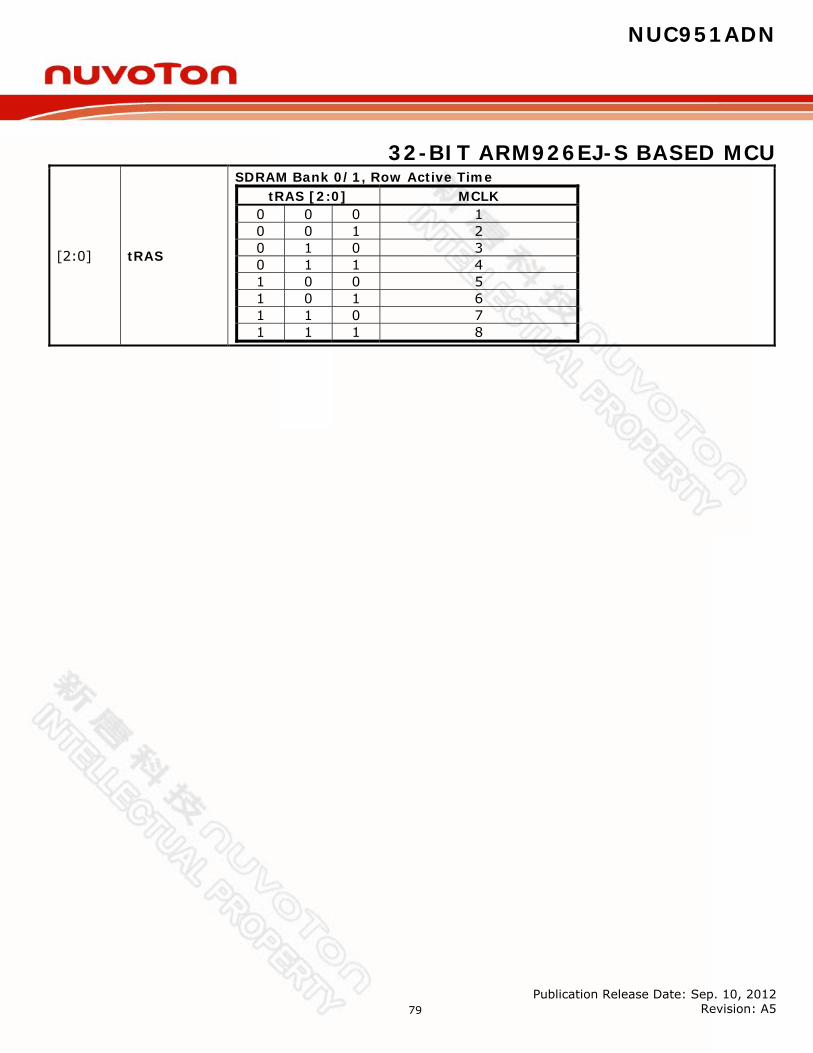
NUC951ADN
32-BIT ARM926EJ-S BASED MCU
Publication Release Date: Sep. 10, 2012 Revision: A5 79
[2:0] tRAS
SDRAM Bank 0/1, Row Active Time tRAS [2:0] MCLK
0 0 0 1 0 0 1 2 0 1 0 3 0 1 1 4 1 0 0 5 1 0 1 6 1 1 0 7 1 1 1 8
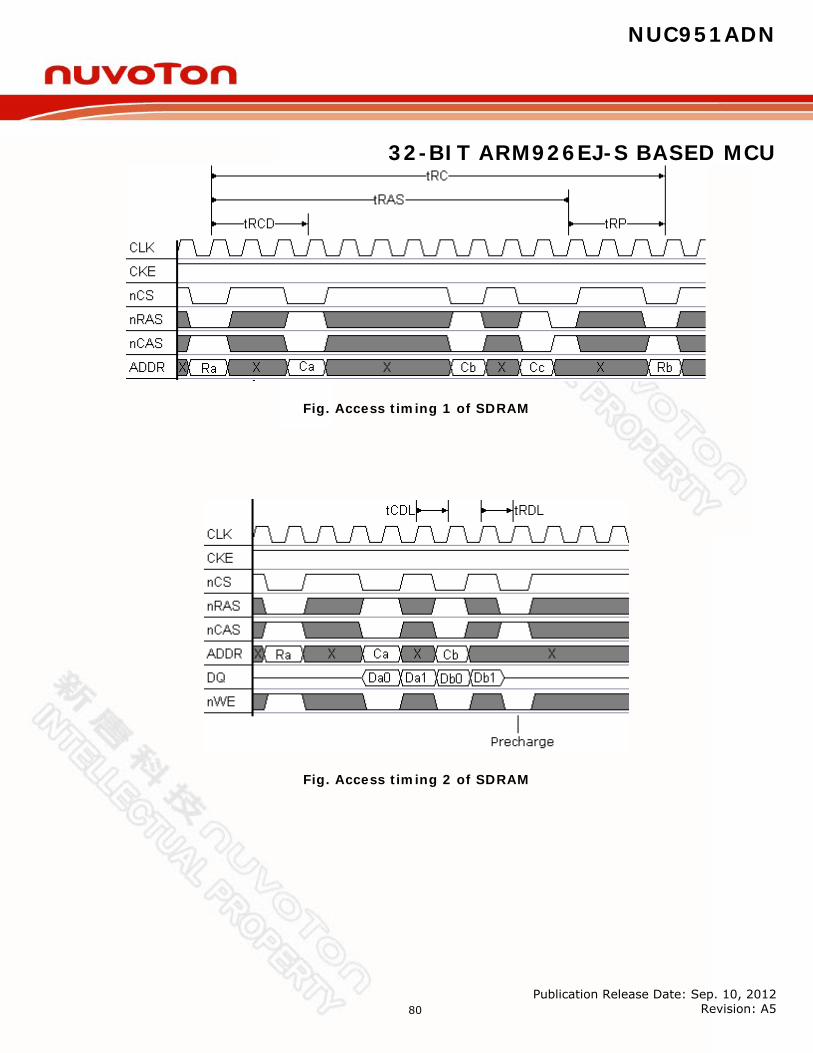
NUC951ADN
32-BIT ARM926EJ-S BASED MCU
Publication Release Date: Sep. 10, 2012 Revision: A5 80
Fig. Access timing 1 of SDRAM
Fig. Access timing 2 of SDRAM
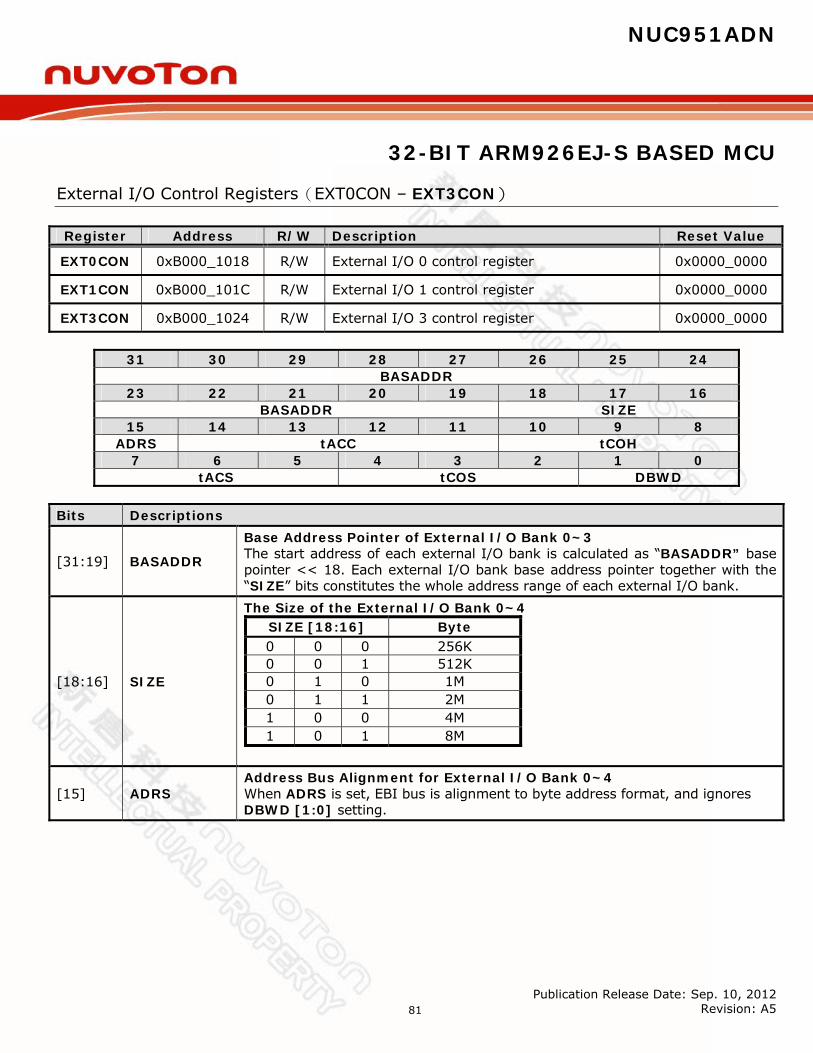
NUC951ADN
32-BIT ARM926EJ-S BASED MCU
Publication Release Date: Sep. 10, 2012 Revision: A5 81
External I/O Control Registers(EXT0CON – EXT3CON)
Register Address R/W Description Reset Value
EXT0CON 0xB000_1018 R/W External I/O 0 control register 0x0000_0000
EXT1CON 0xB000_101C R/W External I/O 1 control register 0x0000_0000
EXT3CON 0xB000_1024 R/W External I/O 3 control register 0x0000_0000
31 30 29 28 27 26 25 24
BASADDR 23 22 21 20 19 18 17 16
BASADDR SIZE 15 14 13 12 11 10 9 8
ADRS tACC tCOH 7 6 5 4 3 2 1 0
tACS tCOS DBWD Bits Descriptions
[31:19] BASADDR
Base Address Pointer of External I/O Bank 0~3 The start address of each external I/O bank is calculated as “BASADDR” base pointer << 18. Each external I/O bank base address pointer together with the “SIZE” bits constitutes the whole address range of each external I/O bank.
[18:16] SIZE
The Size of the External I/O Bank 0~4 SIZE [18:16] Byte 0 0 0 256K 0 0 1 512K 0 1 0 1M 0 1 1 2M 1 0 0 4M 1 0 1 8M
[15] ADRS Address Bus Alignment for External I/O Bank 0~4 When ADRS is set, EBI bus is alignment to byte address format, and ignores DBWD [1:0] setting.

NUC951ADN
32-BIT ARM926EJ-S BASED MCU
Publication Release Date: Sep. 10, 2012 Revision: A5 82
[14:11] tACC
Access Cycles (nOE or nSWE active time)for External I/O Bank 0~4 tACC[14:11] MCLK tACC[14:11] MCLK
0 0 0 0 Reversed 1 0 0 0 9 0 0 0 1 1 1 0 0 1 11 0 0 1 0 2 1 0 1 0 13 0 0 1 1 3 1 0 1 1 15 0 1 0 0 4 1 1 0 0 17 0 1 0 1 5 1 1 0 1 19 0 1 1 0 6 1 1 1 0 21 0 1 1 1 7 1 1 1 1 23
[10:8] tCOH
Chip Selection Hold-On Time on nOE or nWBE for External I/O Bank 0~4 tCOH [10:8] MCLK
0 0 0 0 0 0 1 1 0 1 0 2 0 1 1 3 1 0 0 4 1 0 1 5 1 1 0 6 1 1 1 7
[7:5] tACS
Address Set-up Before nECS for External I/O bank 0~4 tACS [7:5] MCLK
0 0 0 0 0 0 1 1 0 1 0 2 0 1 1 3 1 0 0 4 1 0 1 5 1 1 0 6 1 1 1 7
[4:2] tCOS
Chip Selection Set-up Time on nOE or nWBE for External I/O Bank 0~4 When the bank is configured, the access to its bank stretches chip selection time before the nOE or new signal is activated.
tCOS [4:2] MCLK 0 0 0 0 0 0 1 1 0 1 0 2 0 1 1 3 1 0 0 4 1 0 1 5 1 1 0 6 1 1 1 7

NUC951ADN
32-BIT ARM926EJ-S BASED MCU
Publication Release Date: Sep. 10, 2012 Revision: A5 83
[1:0] DBWD
Programmable Data Bus Width for External I/O Bank 0~4 DBWD [1:0] Width of Data Bus
0 0 Disable bus 0 1 8-bit 1 0 16-bit 1 1 32-bit
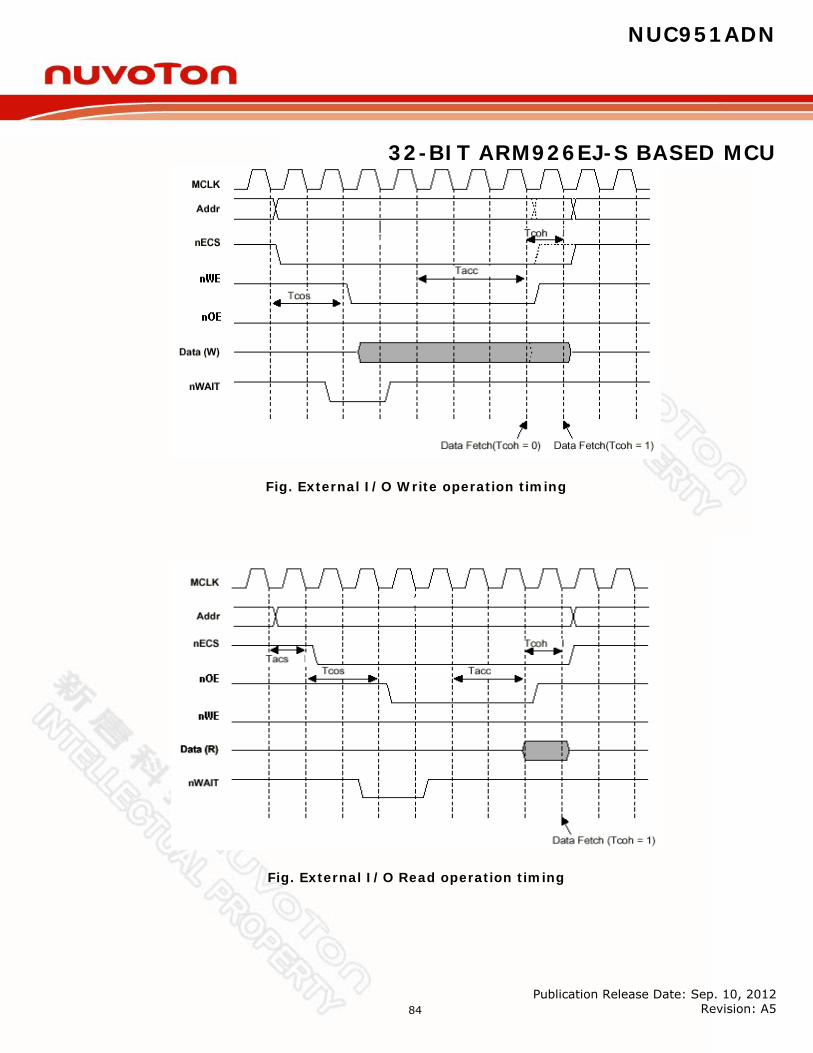
NUC951ADN
32-BIT ARM926EJ-S BASED MCU
Publication Release Date: Sep. 10, 2012 Revision: A5 84
Fig. External I/O Write operation timing
Fig. External I/O Read operation timing

NUC951ADN
32-BIT ARM926EJ-S BASED MCU
Publication Release Date: Sep. 10, 2012 Revision: A5 85
Clock Skew Control Register (CKSKEW)
Register Address R/W Description Reset Value CKSKEW 0xB000_102C R/W Clock Skew Control Register 0xXXXX_0048
31 30 29 28 27 26 25 24
Reserved 23 22 21 20 19 18 17 16
Reserved 15 14 13 12 11 10 9 8
Reserved 7 6 5 4 3 2 1 0
DLH_CLK_SKEW MCLK_O_D Bits Descriptions
[7:4] DLH_CLK_SKEW
Data Latch Clock Skew Adjustment DLH_CLK_SKEW[7:4] Gate
Delay DLH_CLK_SKEW[7:4] Gate
Delay 0 0 0 0 P-0 1 0 0 0 N-0 0 0 0 1 P-1 1 0 0 1 N-1 0 0 1 0 P-2 1 0 1 0 N-2 0 0 1 1 P-3 1 0 1 1 N-3 0 1 0 0 P-4 1 1 0 0 N-4 0 1 0 1 P-5 1 1 0 1 N-5 0 1 1 0 P-6 1 1 1 0 N-6 0 1 1 1 P-7 1 1 1 1 N-7
Note: P-x means Data latched Clock shift “X” gates delays by refer MCLKO positive edge;
N-x means Data latched Clock shift “X” gates delays by refer MCLKO negative edge.
[3:0] MCLK_O_D
MCLK Output Delay Adjustment MCLK_O_D [3:0] Gate
Delay MCLK_O_D [3:0] Gate
Delay 0 0 0 0 P-0 1 0 0 0 N-0 0 0 0 1 P-1 1 0 0 1 N-1 0 0 1 0 P-2 1 0 1 0 N-2 0 0 1 1 P-3 1 0 1 1 N-3 0 1 0 0 P-4 1 1 0 0 N-4 0 1 0 1 P-5 1 1 0 1 N-5 0 1 1 0 P-6 1 1 1 0 N-6 0 1 1 1 P-7 1 1 1 1 N-7
Note: P-x means MCLKO shift “X” gates delay by refer HCLK positive edge; N-x means MCLKO shift “X” gates delay by refer HCLK negative edge. MCLK is the output pin of MCLKO, which is an internal signal on chip.
NUC951ADN
32-BIT ARM926EJ-S BASED MCU
Publication Release Date: Sep. 10, 2012 Revision: A5 86
7.5 Ethernet MAC Controller
Overview This chip provides an Ethernet MAC Controller (EMC) for WAN/LAN application. This EMC has its DMA controller, transmit FIFO, and receive FIFO.
The Ethernet MAC controller consists of IEEE 802.3/Ethernet protocol engine with internal CAM function for Ethernet MAC address recognition, Transmit-FIFO, Receive-FIFO, TX/RX state machine controller and status controller. The EMC only supports RMII (Reduced MII) interface to connect with PHY operating on 50MHz REF_CLK.
Features Supports IEEE Std. 802.3 CSMA/CD protocol. Supports both half and full duplex for 10M/100M bps operation. Supports RMII interface. Supports MII Management function. Supports pause and remote pause function for flow control. Supports long frame (more than 1518 bytes) and short frame (less than 64 bytes) reception. Supports 16 entries CAM function for Ethernet MAC address recognition. Supports internal loop back mode for diagnostic. Supports 256 bytes embedded transmit and receive FIFO. Supports DMA function.
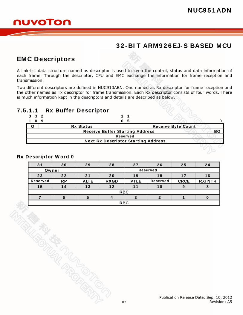
NUC951ADN
32-BIT ARM926EJ-S BASED MCU
Publication Release Date: Sep. 10, 2012 Revision: A5 87
EMC Descriptors A link-list data structure named as descriptor is used to keep the control, status and data information of each frame. Through the descriptor, CPU and EMC exchange the information for frame reception and transmission.
Two different descriptors are defined in NUC910ABN. One named as Rx descriptor for frame reception and the other names as Tx descriptor for frame transmission. Each Rx descriptor consists of four words. There is much information kept in the descriptors and details are described as below.
7.5.1.1 Rx Buffer Descriptor
31
30
29
16
15
0
O Rx Status Receive Byte Count Receive Buffer Starting Address BO
Reserved Next Rx Descriptor Starting Address
Rx Descriptor Word 0
31 30 29 28 27 26 25 24 Owner Reserved
23 22 21 20 19 18 17 16 Reserved RP ALIE RXGD PTLE Reserved CRCE RXINTR
15 14 13 12 11 10 9 8 RBC
7 6 5 4 3 2 1 0 RBC

NUC951ADN
32-BIT ARM926EJ-S BASED MCU
Publication Release Date: Sep. 10, 2012 Revision: A5 88
Bits Descriptions
[31:30] Owner
Ownership The ownership field defines which one, the CPU or EMC, is the owner of each Rx descriptor. Only the owner has right to modify the Rx descriptor and the others can read the Rx descriptor only.
00: The owner is CPU 01: Undefined 10: The owner is EMC 11: Undefined
If the O=2’b10 indicates the EMC RxDMA is the owner of Rx descriptor and the Rx descriptor is available for frame reception. After the frame reception completed, if the frame needed NAT translation, EMC RxDMA modify ownership field to 2’b11. Otherwise, the ownership field will be modified to 2’b00. If the O=2’b00 indicates the CPU is the owner of Rx descriptor. After the CPU completes processing the frame, it modifies the ownership field to 2’b10 and releases the Rx descriptor to EMC RxDMA.
[29:23] Rx Status
Receive Status This field keeps the status for frame reception. All status bits are updated by EMC. In the receive status, bits 29 to 23 are undefined and reserved for the future.
[22] RP
Runt Packet The RP indicates the frame stored in the data buffer pointed by Rx descriptor is a short frame (frame length is less than 64 bytes).
1’b0: The frame is not a short frame. 1’b1: The frame is a short frame.
[21] ALIE
Alignment Error The ALIE indicates the frame stored in the data buffer pointed by Rx descriptor is not a multiple of byte.
1’b0: The frame is a multiple of byte. 1’b1: The frame is not a multiple of byte.
[20] RXGD
Frame Reception Complete The RXGD indicates the frame reception has completed and stored in the data buffer pointed by Rx descriptor.
1’b0: The frame reception not complete yet. 1’b1: The frame reception completed.
[19] PTLE
Packet Too Long The PTLE indicates the frame stored in the data buffer pointed by Rx descriptor is a long frame (frame length is greater than 1518 bytes).
1’b0: The frame is not a long frame. 1’b1: The frame is a long frame.
[17] CRCE
CRC Error The CRCE indicates the frame stored in the data buffer pointed by Rx descriptor incurred CRC error.
1’b0: The frame doesn’t incur CRC error. 1’b1: The frame incurred CRC error.
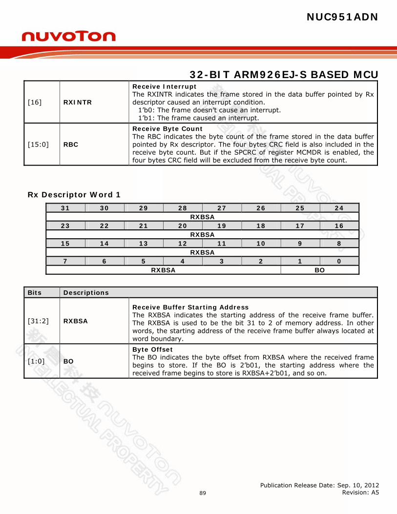
NUC951ADN
32-BIT ARM926EJ-S BASED MCU
Publication Release Date: Sep. 10, 2012 Revision: A5 89
[16] RXINTR
Receive Interrupt The RXINTR indicates the frame stored in the data buffer pointed by Rx descriptor caused an interrupt condition.
1’b0: The frame doesn’t cause an interrupt. 1’b1: The frame caused an interrupt.
[15:0] RBC
Receive Byte Count The RBC indicates the byte count of the frame stored in the data buffer pointed by Rx descriptor. The four bytes CRC field is also included in the receive byte count. But if the SPCRC of register MCMDR is enabled, the four bytes CRC field will be excluded from the receive byte count.
Rx Descriptor Word 1
31 30 29 28 27 26 25 24 RXBSA
23 22 21 20 19 18 17 16 RXBSA
15 14 13 12 11 10 9 8 RXBSA
7 6 5 4 3 2 1 0 RXBSA BO
Bits Descriptions
[31:2] RXBSA
Receive Buffer Starting Address The RXBSA indicates the starting address of the receive frame buffer. The RXBSA is used to be the bit 31 to 2 of memory address. In other words, the starting address of the receive frame buffer always located at word boundary.
[1:0] BO
Byte Offset The BO indicates the byte offset from RXBSA where the received frame begins to store. If the BO is 2’b01, the starting address where the received frame begins to store is RXBSA+2’b01, and so on.
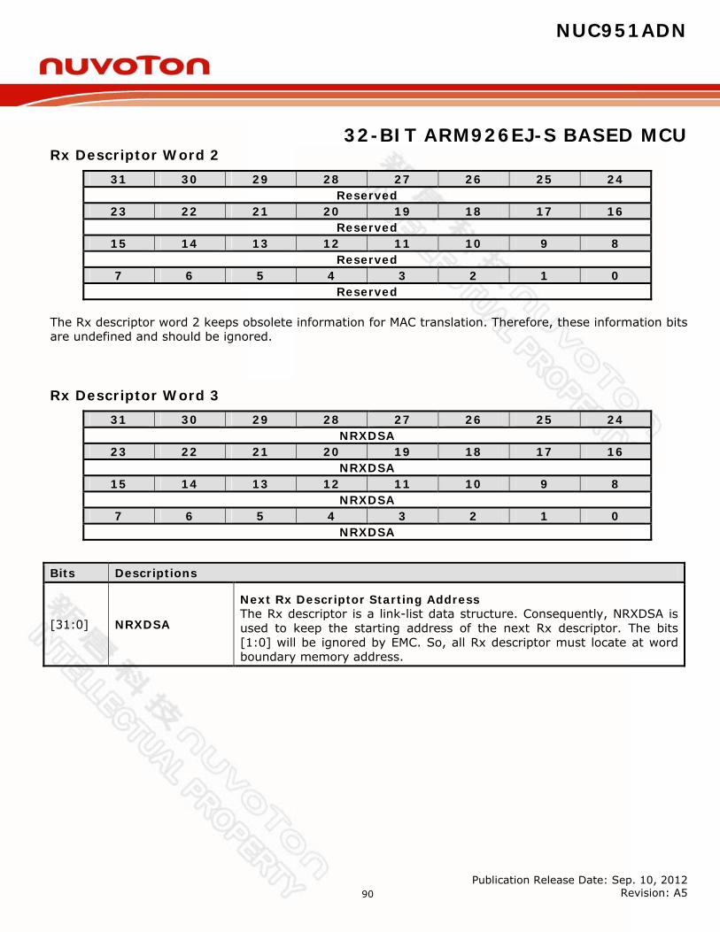
NUC951ADN
32-BIT ARM926EJ-S BASED MCU
Publication Release Date: Sep. 10, 2012 Revision: A5 90
Rx Descriptor Word 2 31 30 29 28 27 26 25 24
Reserved 23 22 21 20 19 18 17 16
Reserved 15 14 13 12 11 10 9 8
Reserved 7 6 5 4 3 2 1 0
Reserved The Rx descriptor word 2 keeps obsolete information for MAC translation. Therefore, these information bits are undefined and should be ignored. Rx Descriptor Word 3
31 30 29 28 27 26 25 24 NRXDSA
23 22 21 20 19 18 17 16 NRXDSA
15 14 13 12 11 10 9 8 NRXDSA
7 6 5 4 3 2 1 0 NRXDSA
Bits Descriptions
[31:0] NRXDSA
Next Rx Descriptor Starting Address The Rx descriptor is a link-list data structure. Consequently, NRXDSA is used to keep the starting address of the next Rx descriptor. The bits [1:0] will be ignored by EMC. So, all Rx descriptor must locate at word boundary memory address.

NUC951ADN
32-BIT ARM926EJ-S BASED MCU
Publication Release Date: Sep. 10, 2012 Revision: A5 91
7.5.1.2 Tx Buffer Descriptor
31
30
16
15
3
2
1
0
O Reserved I C P Transmit Buffer Starting Address BO
Tx Status Transmit Byte Count Next Tx Descriptor Starting Address
Tx Descriptor Word 0
31 30 29 28 27 26 25 24 Owner Reserved
23 22 21 20 19 18 17 16 Reserved
15 14 13 12 11 10 9 8 Reserved
7 6 5 4 3 2 1 0 Reserved IntEn CRCApp PadEn
Bits Descriptions
[31] Owner
Ownership The ownership field defines which one, the CPU or EMC, is the owner of each Tx descriptor. Only the owner has right to modify the Tx descriptor and the other can read the Tx descriptor only.
0: The owner is CPU 1: The owner is EMC
If the O=1’b1 indicates the EMC TxDMA is the owner of Tx descriptor and the Tx descriptor is available for frame transmission. After the frame transmission completed, EMC TxDMA modify ownership field to 1’b0 and return the ownership of Tx descriptor to CPU. If the O=1’b0 indicates the CPU is the owner of Tx descriptor. After the CPU prepares new frame to wait transmission, it modifies the ownership field to 1’b1 and releases the Tx descriptor to EMC TxDMA.
[2] IntEn
Transmit Interrupt Enable The IntEn controls the interrupt trigger circuit after the frame transmission completed. If the IntEn is enabled, the EMC will trigger interrupt after frame transmission completed. Otherwise, the interrupt doesn’t be triggered.
1’b0: Frame transmission interrupt is masked. 1’b1: Frame transmission interrupt is enabled.
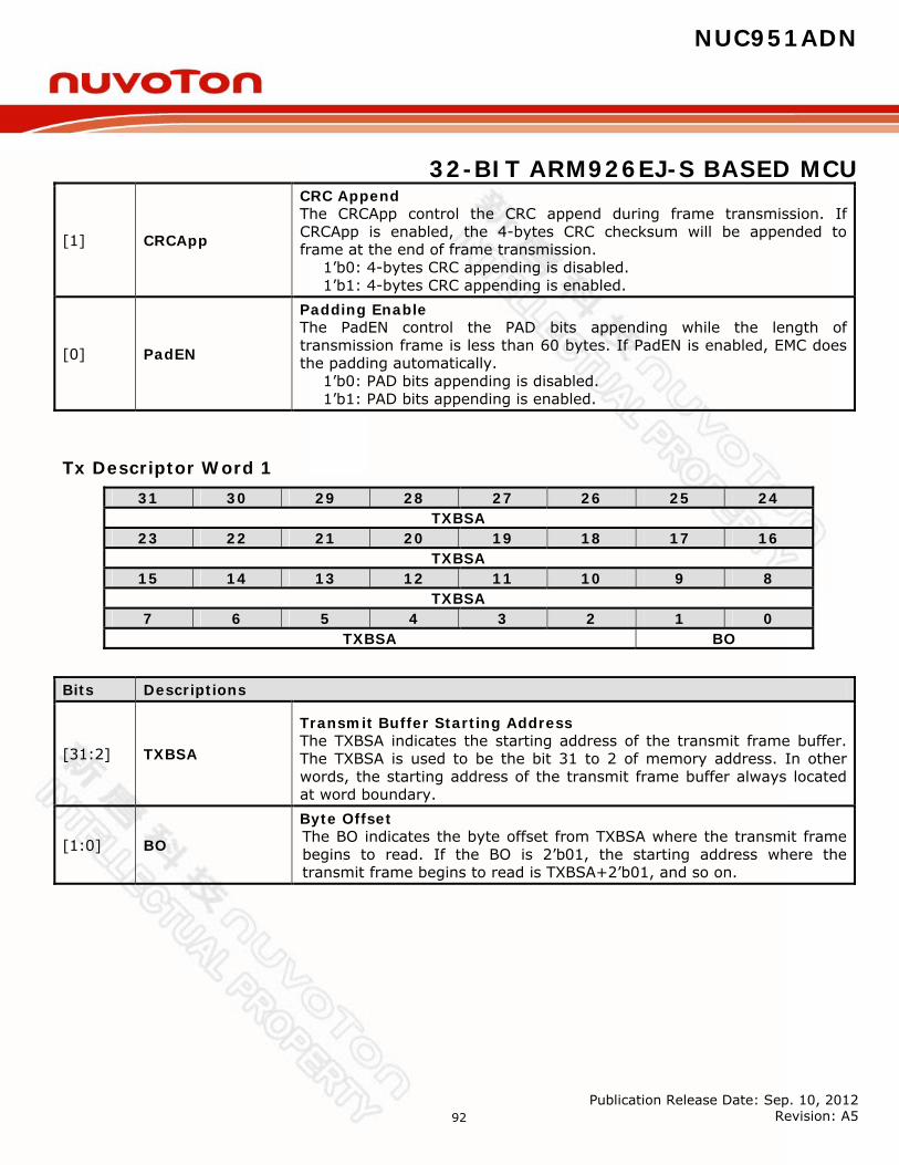
NUC951ADN
32-BIT ARM926EJ-S BASED MCU
Publication Release Date: Sep. 10, 2012 Revision: A5 92
[1] CRCApp
CRC Append The CRCApp control the CRC append during frame transmission. If CRCApp is enabled, the 4-bytes CRC checksum will be appended to frame at the end of frame transmission.
1’b0: 4-bytes CRC appending is disabled. 1’b1: 4-bytes CRC appending is enabled.
[0] PadEN
Padding Enable The PadEN control the PAD bits appending while the length of transmission frame is less than 60 bytes. If PadEN is enabled, EMC does the padding automatically.
1’b0: PAD bits appending is disabled. 1’b1: PAD bits appending is enabled.
Tx Descriptor Word 1
31 30 29 28 27 26 25 24 TXBSA
23 22 21 20 19 18 17 16 TXBSA
15 14 13 12 11 10 9 8 TXBSA
7 6 5 4 3 2 1 0 TXBSA BO
Bits Descriptions
[31:2] TXBSA
Transmit Buffer Starting Address The TXBSA indicates the starting address of the transmit frame buffer. The TXBSA is used to be the bit 31 to 2 of memory address. In other words, the starting address of the transmit frame buffer always located at word boundary.
[1:0] BO
Byte Offset The BO indicates the byte offset from TXBSA where the transmit frame begins to read. If the BO is 2’b01, the starting address where the transmit frame begins to read is TXBSA+2’b01, and so on.

NUC951ADN
32-BIT ARM926EJ-S BASED MCU
Publication Release Date: Sep. 10, 2012 Revision: A5 93
Tx Descriptor Word 2 31 30 29 28 27 26 25 24
CCNT Reserved SQE PAU TXHA 23 22 21 20 19 18 17 16 LC TXABT NCS EXDEF TXCP Reserved DEF TXINTR 15 14 13 12 11 10 9 8
TBC 7 6 5 4 3 2 1 0
TBC
Bits Descriptions
[31:28] CCNT
Collision Count The CCNT indicates the how many collisions occurred consecutively during a packet transmission. If the packet incurred 16 consecutive collisions during transmission, the CCNT will be 4’h0 and bit TXABT will be set to 1.
[26] SQE
SQE Error The SQE indicates the SQE error found at end of packet transmission on 10Mbps half-duplex mode. The SQE error check will only be done while both bit EnSQE of MCMDR is enabled and EMC is operating on 10Mbps half-duplex mode.
1’b0: No SQE error found at end of packet transmission. 1’b0: SQE error found at end of packet transmission.
[25] PAU
Transmission Paused The PAU indicates the next normal packet transmission process will be paused temporally because EMC received a PAUSE control frame, or S/W set bit SDPZ of MCMDR and make EMC to transmit a PAUSE control frame out.
1’b0: Next normal packet transmission process will go on. 1’b1: Next normal packet transmission process will be paused.
[24] TXHA
P Transmission Halted The TXHA indicates the next normal packet transmission process will be halted because the bit TXON of MCMDR is disabled be S/W.
1’b0: Next normal packet transmission process will go on. 1’b1: Next normal packet transmission process will be halted.
[23] LC
Late Collision The LC indicates the collision occurred in the outside of 64 bytes collision window. This means after the 64 bytes of a frame has transmitted out to the network, the collision still occurred. The late collision check will only be done while EMC is operating on half-duplex mode.
1’b0: No collision occurred in the outside of 64 bytes collision window. 1’b1: Collision occurred in the outside of 64 bytes collision window.
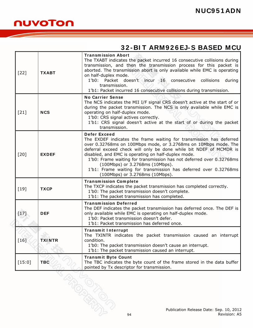
NUC951ADN
32-BIT ARM926EJ-S BASED MCU
Publication Release Date: Sep. 10, 2012 Revision: A5 94
[22] TXABT
Transmission Abort The TXABT indicates the packet incurred 16 consecutive collisions during transmission, and then the transmission process for this packet is aborted. The transmission abort is only available while EMC is operating on half-duplex mode.
1’b0: Packet doesn’t incur 16 consecutive collisions during transmission.
1’b1: Packet incurred 16 consecutive collisions during transmission.
[21] NCS
No Carrier Sense The NCS indicates the MII I/F signal CRS doesn’t active at the start of or during the packet transmission. The NCS is only available while EMC is operating on half-duplex mode.
1’b0: CRS signal actives correctly. 1’b1: CRS signal doesn’t active at the start of or during the packet
transmission.
[20] EXDEF
Defer Exceed The EXDEF indicates the frame waiting for transmission has deferred over 0.32768ms on 100Mbps mode, or 3.2768ms on 10Mbps mode. The deferral exceed check will only be done while bit NDEF of MCMDR is disabled, and EMC is operating on half-duplex mode.
1’b0: Frame waiting for transmission has not deferred over 0.32768ms (100Mbps) or 3.2768ms (10Mbps).
1’b1: Frame waiting for transmission has deferred over 0.32768ms (100Mbps) or 3.2768ms (10Mbps).
[19] TXCP
Transmission Complete The TXCP indicates the packet transmission has completed correctly.
1’b0: The packet transmission doesn’t complete. 1’b1: The packet transmission has completed.
[17] DEF
Transmission Deferred The DEF indicates the packet transmission has deferred once. The DEF is only available while EMC is operating on half-duplex mode.
1’b0: Packet transmission doesn’t defer. 1’b1: Packet transmission has deferred once.
[16] TXINTR
Transmit Interrupt The TXINTR indicates the packet transmission caused an interrupt condition.
1’b0: The packet transmission doesn’t cause an interrupt. 1’b1: The packet transmission caused an interrupt.
[15:0] TBC Transmit Byte Count The TBC indicates the byte count of the frame stored in the data buffer pointed by Tx descriptor for transmission.
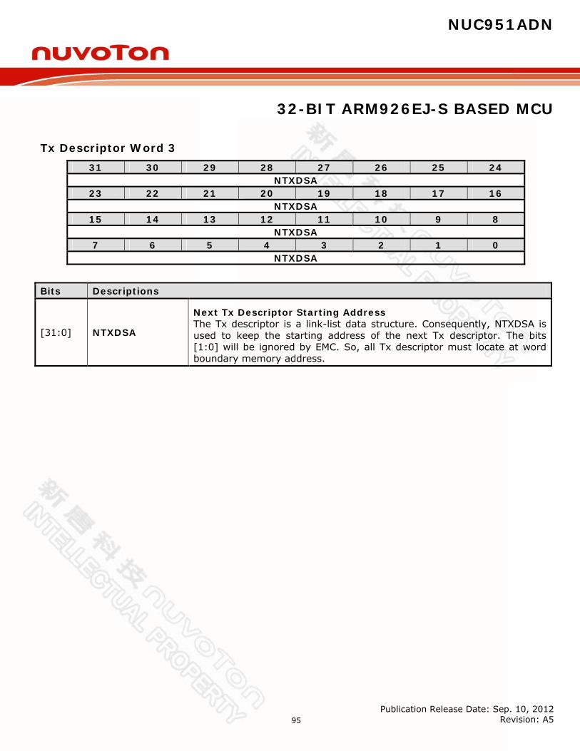
NUC951ADN
32-BIT ARM926EJ-S BASED MCU
Publication Release Date: Sep. 10, 2012 Revision: A5 95
Tx Descriptor Word 3
31 30 29 28 27 26 25 24 NTXDSA
23 22 21 20 19 18 17 16 NTXDSA
15 14 13 12 11 10 9 8 NTXDSA
7 6 5 4 3 2 1 0 NTXDSA
Bits Descriptions
[31:0] NTXDSA
Next Tx Descriptor Starting Address The Tx descriptor is a link-list data structure. Consequently, NTXDSA is used to keep the starting address of the next Tx descriptor. The bits [1:0] will be ignored by EMC. So, all Tx descriptor must locate at word boundary memory address.

NUC951ADN
32-BIT ARM926EJ-S BASED MCU
Publication Release Date: Sep. 10, 2012 Revision: A5 96
7.5.2 EMC Register Mapping The EMC implements many registers and the registers are separated into two types, the control registers and the status registers. The control registers are used by S/W to pass control information to EMC. The status registers are used to keep EMC operation status for S/W. EMC Registers Register Address R/W Description Reset Value
EMC_BA = 0xB000_3000
Control Registers (44) CAMCMR 0xB000_3000 R/W CAM Command Register 0x0000_0000 CAMEN 0xB000_3004 R/W CAM Enable Register 0x0000_0000 CAM0M 0xB000_3008 R/W CAM0 Most Significant Word Register 0x0000_0000 CAM0L 0xB000_300C R/W CAM0 Least Significant Word Register 0x0000_0000 CAM1M 0xB000_3010 R/W CAM1 Most Significant Word Register 0x0000_0000 CAM1L 0xB000_3014 R/W CAM1 Least Significant Word Register 0x0000_0000 CAM2M 0xB000_3018 R/W CAM2 Most Significant Word Register 0x0000_0000 CAM2L 0xB000_301C R/W CAM2 Least Significant Word Register 0x0000_0000 CAM3M 0xB000_3020 R/W CAM3 Most Significant Word Register 0x0000_0000 CAM3L 0xB000_3024 R/W CAM3 Least Significant Word Register 0x0000_0000 CAM4M 0xB000_3028 R/W CAM4 Most Significant Word Register 0x0000_0000 CAM4L 0xB000_302C R/W CAM4 Least Significant Word Register 0x0000_0000 CAM5M 0xB000_3030 R/W CAM5 Most Significant Word Register 0x0000_0000 CAM5L 0xB000_3034 R/W CAM5 Least Significant Word Register 0x0000_0000 CAM6M 0xB000_3038 R/W CAM6 Most Significant Word Register 0x0000_0000 CAM6L 0xB000_303C R/W CAM6 Least Significant Word Register 0x0000_0000 CAM7M 0xB000_3040 R/W CAM7 Most Significant Word Register 0x0000_0000 CAM7L 0xB000_3044 R/W CAM7 Least Significant Word Register 0x0000_0000 CAM8M 0xB000_3048 R/W CAM8 Most Significant Word Register 0x0000_0000 CAM8L 0xB000_304C R/W CAM8 Least Significant Word Register 0x0000_0000 CAM9M 0xB000_3050 R/W CAM9 Most Significant Word Register 0x0000_0000 CAM9L 0xB000_3054 R/W CAM9 Least Significant Word Register 0x0000_0000 CAM10M 0xB000_3058 R/W CAM10 Most Significant Word Register 0x0000_0000 CAM10L 0xB000_305C R/W CAM10 Least Significant Word Register 0x0000_0000 CAM11M 0xB000_3060 R/W CAM11 Most Significant Word Register 0x0000_0000 CAM11L 0xB000_3064 R/W CAM11 Least Significant Word Register 0x0000_0000 CAM12M 0xB000_3068 R/W CAM12 Most Significant Word Register 0x0000_0000 CAM12L 0xB000_306C R/W CAM12 Least Significant Word Register 0x0000_0000 CAM13M 0xB000_3070 R/W CAM13 Most Significant Word Register 0x0000_0000 CAM13L 0xB000_3074 R/W CAM13 Least Significant Word Register 0x0000_0000 CAM14M 0xB000_3078 R/W CAM14 Most Significant Word Register 0x0000_0000 CAM14L 0xB000_307C R/W CAM14 Least Significant Word Register 0x0000_0000 CAM15M 0xB000_3080 R/W CAM15 Most Significant Word Register 0x0000_0000 CAM15L 0xB000_3084 R/W CAM15 Least Significant Word Register 0x0000_0000 TXDLSA 0xB000_3088 R/W Transmit Descriptor Link List Start Address Register 0xFFFF_FFFC
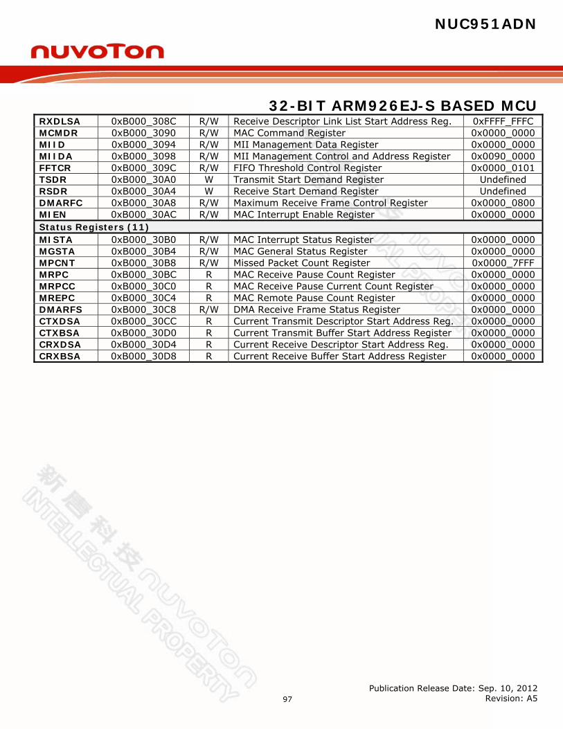
NUC951ADN
32-BIT ARM926EJ-S BASED MCU
Publication Release Date: Sep. 10, 2012 Revision: A5 97
RXDLSA 0xB000_308C R/W Receive Descriptor Link List Start Address Reg. 0xFFFF_FFFC MCMDR 0xB000_3090 R/W MAC Command Register 0x0000_0000 MIID 0xB000_3094 R/W MII Management Data Register 0x0000_0000 MIIDA 0xB000_3098 R/W MII Management Control and Address Register 0x0090_0000 FFTCR 0xB000_309C R/W FIFO Threshold Control Register 0x0000_0101 TSDR 0xB000_30A0 W Transmit Start Demand Register Undefined RSDR 0xB000_30A4 W Receive Start Demand Register Undefined DMARFC 0xB000_30A8 R/W Maximum Receive Frame Control Register 0x0000_0800 MIEN 0xB000_30AC R/W MAC Interrupt Enable Register 0x0000_0000 Status Registers (11) MISTA 0xB000_30B0 R/W MAC Interrupt Status Register 0x0000_0000 MGSTA 0xB000_30B4 R/W MAC General Status Register 0x0000_0000 MPCNT 0xB000_30B8 R/W Missed Packet Count Register 0x0000_7FFF MRPC 0xB000_30BC R MAC Receive Pause Count Register 0x0000_0000 MRPCC 0xB000_30C0 R MAC Receive Pause Current Count Register 0x0000_0000 MREPC 0xB000_30C4 R MAC Remote Pause Count Register 0x0000_0000 DMARFS 0xB000_30C8 R/W DMA Receive Frame Status Register 0x0000_0000 CTXDSA 0xB000_30CC R Current Transmit Descriptor Start Address Reg. 0x0000_0000 CTXBSA 0xB000_30D0 R Current Transmit Buffer Start Address Register 0x0000_0000 CRXDSA 0xB000_30D4 R Current Receive Descriptor Start Address Reg. 0x0000_0000 CRXBSA 0xB000_30D8 R Current Receive Buffer Start Address Register 0x0000_0000

NUC951ADN
32-BIT ARM926EJ-S BASED MCU
Publication Release Date: Sep. 10, 2012 Revision: A5
98
7.5.3 EMC Register Details
CAM Command Register (CAMCMR)
The EMC of NUC910ABN supports CAM function for destination MAC address recognition. The CAMCMR control the CAM comparison function, and unicast, multicast, and broadcast packet reception. Register Address R/W Description Reset Value CAMCMR 0xB000_3000 R/W CAM Command Register 0x0000_0000
31 30 29 28 27 26 25 24
Reserved 23 22 21 20 19 18 17 16
Reserved 15 14 13 12 11 10 9 8
Reserved 7 6 5 4 3 2 1 0
Reserved RMII ECMP CCAM ABP AMP AUP Bits Descriptions
[5] RMII Enable RMII Input Data Sampled by Negative Edge of REFCLK 1’b0: PHY_CRSDV and PHY_RXD[1:0] are sampled by the positive edge of REFCLK 1’b1: PHY_CRSDV and PHY_RxD[1:0] are sampled by the negative edge of REFCLK
[4] ECMP
Enable CAM Compare The ECMP controls the enable of CAM comparison function for destination MAC address recognition. If S/W wants to receive a packet with specific destination MAC address, configures the MAC address into anyone of 16 CAM entries, then enables that CAM entry and set ECMP to 1. 1’b0: Disable CAM comparison function for destination MAC address recognition. 1’b1: Enable CAM comparison function for destination MAC address recognition.
[3] CCAM
Complement CAM Compare The CCAM controls the complement of the CAM comparison result. If the ECMP and CCAM are both enabled, the incoming packet with specific destination MAC address configured in CAM entry will be dropped. And the incoming packet with destination MAC address doesn’t configured in any CAM entry will be received. 1’b0: The CAM comparison result doesn’t be complemented. 1’b1: The CAM comparison result will be complemented.
[2] ABP
Accept Broadcast Packet The ABP controls the broadcast packet reception. If ABP is enabled, EMC receives all incoming packet its destination MAC address is a broadcast address. 1’b0: EMC receives packet depends on the CAM comparison result. 1’b1: EMC receives all broadcast packets.

NUC951ADN
32-BIT ARM926EJ-S BASED MCU
Publication Release Date: Sep. 10, 2012 Revision: A5
99
[1] AMP
Accept Multicast Packet The AMP controls the multicast packet reception. If AMP is enabled, EMC receives all incoming packet its destination MAC address is a multicast address. 1’b0: EMC receives packet depends on the CAM comparison result. 1’b1: EMC receives all multicast packets.
[0] AUP
Accept Unicast Packet The AUP controls the unicast packet reception. If AUP is enabled, EMC receives all incoming packet its destination MAC address is a unicast address. 1’b0: EMC receives packet depends on the CAM comparison result. 1’b1: EMC receives all unicast packets.
CAMCMR Setting and Comparison Result The following table is the address recognition result in different CAMCMR configuration. The column Result shows the incoming packet type that can pass the address recognition in specific CAM configuration. The C, U, M and B represents the: C: It indicates the destination MAC address of incoming packet has been configured in CAM entry. U: It indicates the incoming packet is a unicast packet. M: It indicates the incoming packet is a multicast packet. B: It indicates the incoming packet is a broadcast packet.
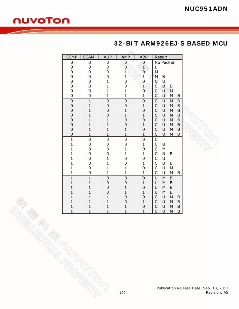
NUC951ADN
32-BIT ARM926EJ-S BASED MCU
Publication Release Date: Sep. 10, 2012 Revision: A5
100
ECMP CCAM AUP AMP ABP Result 0 0 0 0 0 No Packet 0 0 0 0 1 B 0 0 0 1 0 M 0 0 0 1 1 M B 0 0 1 0 0 C U 0 0 1 0 1 C U B 0 0 1 1 0 C U M 0 0 1 1 1 C U M B 0 1 0 0 0 C U M B 0 1 0 0 1 C U M B 0 1 0 1 0 C U M B 0 1 0 1 1 C U M B 0 1 1 0 0 C U M B 0 1 1 0 1 C U M B 0 1 1 1 0 C U M B 0 1 1 1 1 C U M B 1 0 0 0 0 C 1 0 0 0 1 C B 1 0 0 1 0 C M 1 0 0 1 1 C N B 1 0 1 0 0 C U 1 0 1 0 1 C U B 1 0 1 1 0 C U M 1 0 1 1 1 C U M B 1 1 0 0 0 U M B 1 1 0 0 1 U M B 1 1 0 1 0 U M B 1 1 0 1 1 U M B 1 1 1 0 0 C U M B 1 1 1 0 1 C U M B 1 1 1 1 0 C U M B 1 1 1 1 1 C U M B
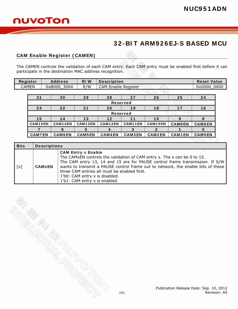
NUC951ADN
32-BIT ARM926EJ-S BASED MCU
Publication Release Date: Sep. 10, 2012 Revision: A5
101
CAM Enable Register (CAMEN)
The CAMEN controls the validation of each CAM entry. Each CAM entry must be enabled first before it can participate in the destination MAC address recognition. Register Address R/W Description Reset Value CAMEN 0xB000_3004 R/W CAM Enable Register 0x0000_0000
31 30 29 28 27 26 25 24
Reserved 23 22 21 20 19 18 17 16
Reserved 15 14 13 12 11 10 9 8
CAM15EN CAM14EN CAM13EN CAM12EN CAM11EN CAM10EN CAM9EN CAM8EN 7 6 5 4 3 2 1 0
CAM7EN CAM6EN CAM5EN CAM4EN CAM3EN CAM2EN CAM1EN CAM0EN Bits Descriptions
[x] CAMxEN
CAM Entry x Enable The CAMxEN controls the validation of CAM entry x. The x can be 0 to 15. The CAM entry 13, 14 and 15 are for PAUSE control frame transmission. If S/W wants to transmit a PAUSE control frame out to network, the enable bits of these three CAM entries all must be enabled first. 1’b0: CAM entry x is disabled. 1’b1: CAM entry x is enabled.
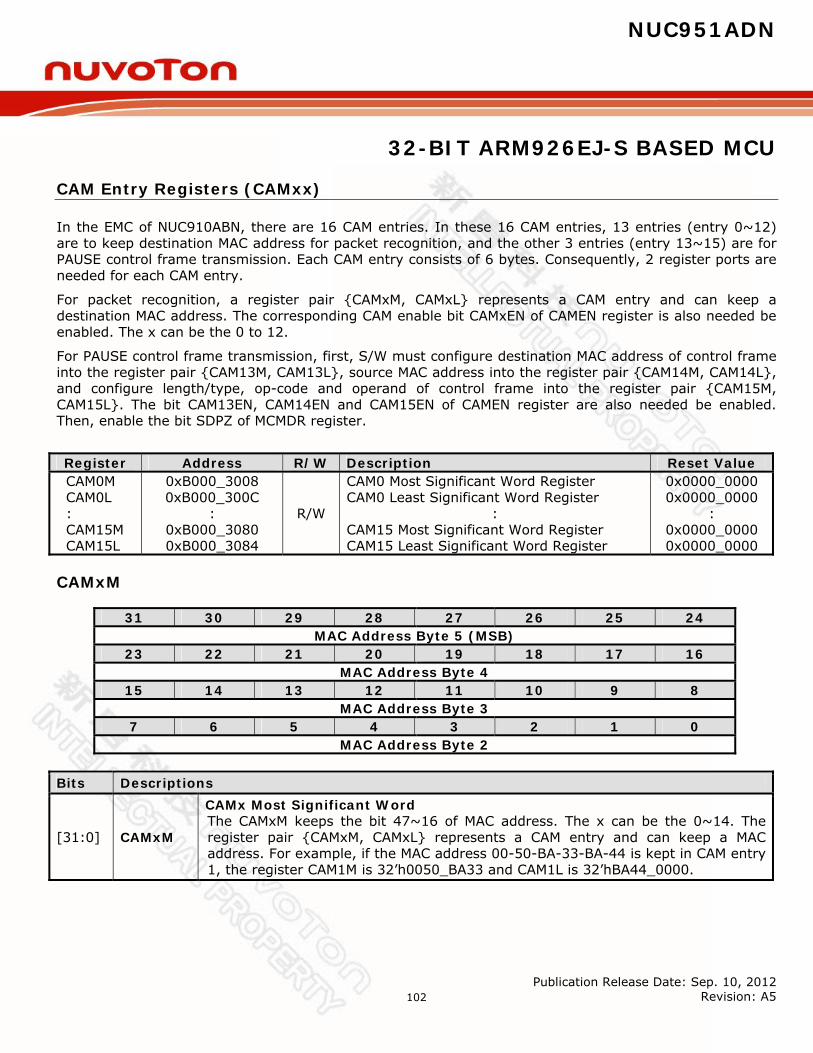
NUC951ADN
32-BIT ARM926EJ-S BASED MCU
Publication Release Date: Sep. 10, 2012 Revision: A5
102
CAM Entry Registers (CAMxx)
In the EMC of NUC910ABN, there are 16 CAM entries. In these 16 CAM entries, 13 entries (entry 0~12) are to keep destination MAC address for packet recognition, and the other 3 entries (entry 13~15) are for PAUSE control frame transmission. Each CAM entry consists of 6 bytes. Consequently, 2 register ports are needed for each CAM entry.
For packet recognition, a register pair CAMxM, CAMxL represents a CAM entry and can keep a destination MAC address. The corresponding CAM enable bit CAMxEN of CAMEN register is also needed be enabled. The x can be the 0 to 12.
For PAUSE control frame transmission, first, S/W must configure destination MAC address of control frame into the register pair CAM13M, CAM13L, source MAC address into the register pair CAM14M, CAM14L, and configure length/type, op-code and operand of control frame into the register pair CAM15M, CAM15L. The bit CAM13EN, CAM14EN and CAM15EN of CAMEN register are also needed be enabled. Then, enable the bit SDPZ of MCMDR register.
Register Address R/W Description Reset Value CAM0M CAM0L : CAM15M CAM15L
0xB000_3008 0xB000_300C
: 0xB000_3080 0xB000_3084
R/W
CAM0 Most Significant Word Register CAM0 Least Significant Word Register
: CAM15 Most Significant Word Register CAM15 Least Significant Word Register
0x0000_0000 0x0000_0000
: 0x0000_0000 0x0000_0000
CAMxM
31 30 29 28 27 26 25 24 MAC Address Byte 5 (MSB)
23 22 21 20 19 18 17 16 MAC Address Byte 4
15 14 13 12 11 10 9 8 MAC Address Byte 3
7 6 5 4 3 2 1 0 MAC Address Byte 2
Bits Descriptions
[31:0] CAMxM
CAMx Most Significant Word The CAMxM keeps the bit 47~16 of MAC address. The x can be the 0~14. The register pair CAMxM, CAMxL represents a CAM entry and can keep a MAC address. For example, if the MAC address 00-50-BA-33-BA-44 is kept in CAM entry 1, the register CAM1M is 32’h0050_BA33 and CAM1L is 32’hBA44_0000.
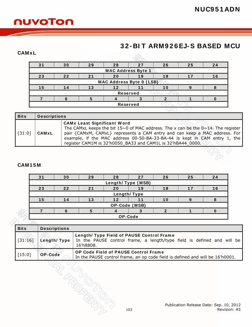
NUC951ADN
32-BIT ARM926EJ-S BASED MCU
Publication Release Date: Sep. 10, 2012 Revision: A5
103
CAMxL
31 30 29 28 27 26 25 24 MAC Address Byte 1
23 22 21 20 19 18 17 16 MAC Address Byte 0 (LSB)
15 14 13 12 11 10 9 8 Reserved
7 6 5 4 3 2 1 0 Reserved
Bits Descriptions
[31:0] CAMxL
CAMx Least Significant Word The CAMxL keeps the bit 15~0 of MAC address. The x can be the 0~14. The register pair CAMxM, CAMxL represents a CAM entry and can keep a MAC address. For example, if the MAC address 00-50-BA-33-BA-44 is kept in CAM entry 1, the register CAM1M is 32’h0050_BA33 and CAM1L is 32’hBA44_0000.
CAM15M
31 30 29 28 27 26 25 24 Length/Type (MSB)
23 22 21 20 19 18 17 16 Length/Type
15 14 13 12 11 10 9 8 OP-Code (MSB)
7 6 5 4 3 2 1 0 OP-Code
Bits Descriptions
[31:16] Length/Type Length/Type Field of PAUSE Control Frame In the PAUSE control frame, a length/type field is defined and will be 16’h8808.
[15:0] OP-Code OP Code Field of PAUSE Control Frame In the PAUSE control frame, an op code field is defined and will be 16’h0001.
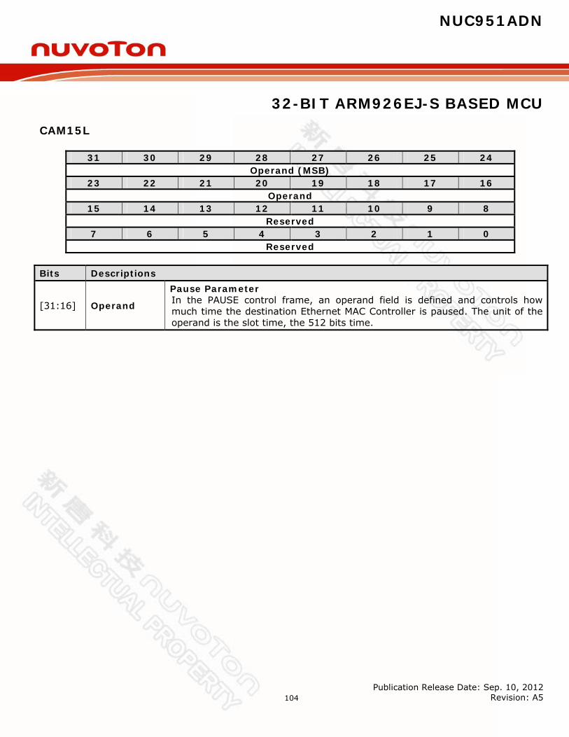
NUC951ADN
32-BIT ARM926EJ-S BASED MCU
Publication Release Date: Sep. 10, 2012 Revision: A5
104
CAM15L
31 30 29 28 27 26 25 24 Operand (MSB)
23 22 21 20 19 18 17 16 Operand
15 14 13 12 11 10 9 8 Reserved
7 6 5 4 3 2 1 0 Reserved
Bits Descriptions
[31:16] Operand
Pause Parameter In the PAUSE control frame, an operand field is defined and controls how much time the destination Ethernet MAC Controller is paused. The unit of the operand is the slot time, the 512 bits time.
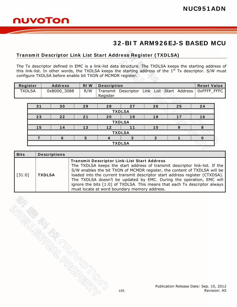
NUC951ADN
32-BIT ARM926EJ-S BASED MCU
Publication Release Date: Sep. 10, 2012 Revision: A5
105
Transmit Descriptor Link List Start Address Register (TXDLSA)
The Tx descriptor defined in EMC is a link-list data structure. The TXDLSA keeps the starting address of this link-list. In other words, the TXDLSA keeps the starting address of the 1st Tx descriptor. S/W must configure TXDLSA before enable bit TXON of MCMDR register. Register Address R/W Description Reset Value TXDLSA 0xB000_3088 R/W Transmit Descriptor Link List Start Address
Register 0xFFFF_FFFC
31 30 29 28 27 26 25 24
TXDLSA 23 22 21 20 19 18 17 16
TXDLSA 15 14 13 12 11 10 9 8
TXDLSA 7 6 5 4 3 2 1 0
TXDLSA Bits Descriptions
[31:0] TXDLSA
Transmit Descriptor Link-List Start Address The TXDLSA keeps the start address of transmit descriptor link-list. If the S/W enables the bit TXON of MCMDR register, the content of TXDLSA will be loaded into the current transmit descriptor start address register (CTXDSA). The TXDLSA doesn’t be updated by EMC. During the operation, EMC will ignore the bits [1:0] of TXDLSA. This means that each Tx descriptor always must locate at word boundary memory address.

NUC951ADN
32-BIT ARM926EJ-S BASED MCU
Publication Release Date: Sep. 10, 2012 Revision: A5
106
Receive Descriptor Link List Start Address Register (RXDLSA)
The Rx descriptor defined in EMC is a link-list data structure. The RXDLSA keeps the starting address of this link-list. In other words, the RXDLSA keeps the starting address of the 1st Rx descriptor. S/W must configure RXDLSA before enable bit RXON of MCMDR register. Register Address R/W Description Reset Value RXDLSA 0xB000_308C R/W Receive Descriptor Link List Start Address
Register 0xFFFF_FFFC
31 30 29 28 27 26 25 24
RXDLSA 23 22 21 20 19 18 17 16
RXDLSA 15 14 13 12 11 10 9 8
RXDLSA 7 6 5 4 3 2 1 0
RXDLSA Bits Descriptions
[31:0] RTXDLSA
Receive Descriptor Link-List Start Address The RXDLSA keeps the start address of receive descriptor link-list. If the S/W enables the bit RXON of MCMDR register, the content of RXDLSA will be loaded into the current receive descriptor start address register (CRXDSA). The RXDLSA doesn’t be updated by EMC. During the operation, EMC will ignore the bits [1:0] of RXDLSA. This means that each Rx descriptor always must locate at word boundary memory address.

NUC951ADN
32-BIT ARM926EJ-S BASED MCU
Publication Release Date: Sep. 10, 2012 Revision: A5
107
MAC Command Register (MCMDR)
The MCMDR provides the control information for EMC. Some command settings affect both frame transmission and reception, such as bit FDUP, the full/half duplex mode selection, or bit OPMOD, the 100/10M bps mode selection. Some command settings control frame transmission and reception separately, likes bit TXON and RXON. Register Address R/W Description Reset Value MCMDR 0xB000_3090 R/W MAC Command Register 0x0000_0000
31 30 29 28 27 26 25 24
Reserved SWR 23 22 21 20 19 18 17 16
Reserved LBK OPMOD EnMDC FDUP EnSQE SDPZ 15 14 13 12 11 10 9 8
Reserved NDEF TXON 7 6 5 4 3 2 1 0
Reserved SPCRC AEP ACP ARP ALP RXON Bits Descriptions
[24] SWR
Software Reset The SWR implements a reset function to make the EMC return default state. The SWR is a self-clear bit. This means after the software reset finished, the SWR will be cleared automatically. Enable SWR can also reset all control and status registers, exclusive of these two bits EnRMII and OPMOD of MCMDR register. The EMC re-initial is needed after the software reset completed. 1’b0: Software reset completed. 1’b1: Enable software reset.
[21] LBK
Internal Loop Back Select The LBK enables the EMC operating on internal loop-back mode. If the LBK is enabled, the packet transmitted out will be loop-backed to Rx. If the EMC is operating on internal loop-back mode, it also means the EMC is operating on full-duplex mode and the value of FDUP of MCMDR register is ignored. Beside, the LBK doesn’t be affected by SWR bit. 1’b0: The EMC operates in normal mode. 1’b1: The EMC operates in internal loop-back mode.
[20] OPMOD
Operation Mode Select The OPMOD defines the EMC is operating on 10M or 100M bps mode. The OPMOD doesn’t be affected by SWR bit. 1’b0: The EMC operates on 10Mbps mode. 1’b1: The EMC operates on 100Mbps mode.

NUC951ADN
32-BIT ARM926EJ-S BASED MCU
Publication Release Date: Sep. 10, 2012 Revision: A5
108
[19] EnMDC
Enable MDC Clock Generation The EnMDC controls the MDC clock generation for MII Management Interface. If the EnMDC is set to 1, the MDC clock generation is enabled. Otherwise, the MDC clock generation is disabled. Consequently, if S/W wants to access the registers of external PHY through MII Management Interface, the EnMDC must be set to high. 1’b0: Disable MDC clock generation. 1’b1: Enable MDC clock generation.
[18] FDUP
Full Duplex Mode Select The FDUP controls that EMC is operating on full or half duplex mode. 1’b0: The EMC operates on half duplex mode. 1’b1: The EMC operates on full duplex mode.
[17] EnSQE
Enable SQE Checking The EnSQE controls the enable of SQE checking. The SQE checking is only available while EMC is operating on 10M bps and half duplex mode. In other words, the EnSQE cannot affect EMC operation, if the EMC is operating on 100M bps or full duplex mode. 1’b0: Disable SQE checking while EMC is operating on 10Mbps and half
duplex mode. 1’b1: Enable SQE checking while EMC is operating on 10Mbps and half
duplex mode.
[16] SDPZ
Send PAUSE Frame The SDPZ controls the PAUSE control frame transmission. If S/W wants to send a PAUSE control frame out, the CAM entry 13, 14 and 15 must be configured first and the corresponding CAM enable bit of CAMEN register also must be set. Then, set SDPZ to 1 enables the PAUSE control frame transmission. The SDPZ is a self-clear bit. This means after the PAUSE control frame transmission has completed, the SDPZ will be cleared automatically. It is recommended that only enables SPDZ while EMC is operating on full duplex mode. 1’b0: The PAUSE control frame transmission has completed. 1’b1: Enable EMC to transmit a PAUSE control frame out.
[9] NDEF
No Defer The NDEF controls the enable of deferral exceed counter. If NDEF is set to high, the deferral exceed counter is disabled. The NDEF is only useful while EMC is operating on half duplex mode. 1’b0: The deferral exceed counter is enabled. 1’b1: The deferral exceed counter is disabled.
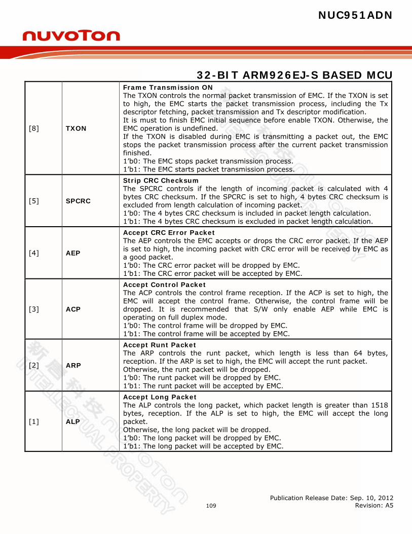
NUC951ADN
32-BIT ARM926EJ-S BASED MCU
Publication Release Date: Sep. 10, 2012 Revision: A5
109
[8] TXON
Frame Transmission ON The TXON controls the normal packet transmission of EMC. If the TXON is set to high, the EMC starts the packet transmission process, including the Tx descriptor fetching, packet transmission and Tx descriptor modification. It is must to finish EMC initial sequence before enable TXON. Otherwise, the EMC operation is undefined. If the TXON is disabled during EMC is transmitting a packet out, the EMC stops the packet transmission process after the current packet transmission finished. 1’b0: The EMC stops packet transmission process. 1’b1: The EMC starts packet transmission process.
[5] SPCRC
Strip CRC Checksum The SPCRC controls if the length of incoming packet is calculated with 4 bytes CRC checksum. If the SPCRC is set to high, 4 bytes CRC checksum is excluded from length calculation of incoming packet. 1’b0: The 4 bytes CRC checksum is included in packet length calculation. 1’b1: The 4 bytes CRC checksum is excluded in packet length calculation.
[4] AEP
Accept CRC Error Packet The AEP controls the EMC accepts or drops the CRC error packet. If the AEP is set to high, the incoming packet with CRC error will be received by EMC as a good packet. 1’b0: The CRC error packet will be dropped by EMC. 1’b1: The CRC error packet will be accepted by EMC.
[3] ACP
Accept Control Packet The ACP controls the control frame reception. If the ACP is set to high, the EMC will accept the control frame. Otherwise, the control frame will be dropped. It is recommended that S/W only enable AEP while EMC is operating on full duplex mode. 1’b0: The control frame will be dropped by EMC. 1’b1: The control frame will be accepted by EMC.
[2] ARP
Accept Runt Packet The ARP controls the runt packet, which length is less than 64 bytes, reception. If the ARP is set to high, the EMC will accept the runt packet. Otherwise, the runt packet will be dropped. 1’b0: The runt packet will be dropped by EMC. 1’b1: The runt packet will be accepted by EMC.
[1] ALP
Accept Long Packet The ALP controls the long packet, which packet length is greater than 1518 bytes, reception. If the ALP is set to high, the EMC will accept the long packet. Otherwise, the long packet will be dropped. 1’b0: The long packet will be dropped by EMC. 1’b1: The long packet will be accepted by EMC.
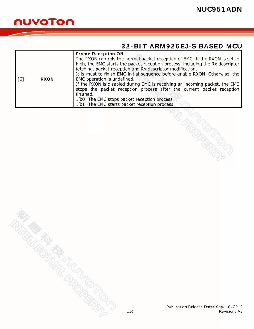
NUC951ADN
32-BIT ARM926EJ-S BASED MCU
Publication Release Date: Sep. 10, 2012 Revision: A5
110
[0] RXON
Frame Reception ON The RXON controls the normal packet reception of EMC. If the RXON is set to high, the EMC starts the packet reception process, including the Rx descriptor fetching, packet reception and Rx descriptor modification. It is must to finish EMC initial sequence before enable RXON. Otherwise, the EMC operation is undefined. If the RXON is disabled during EMC is receiving an incoming packet, the EMC stops the packet reception process after the current packet reception finished. 1’b0: The EMC stops packet reception process. 1’b1: The EMC starts packet reception process.
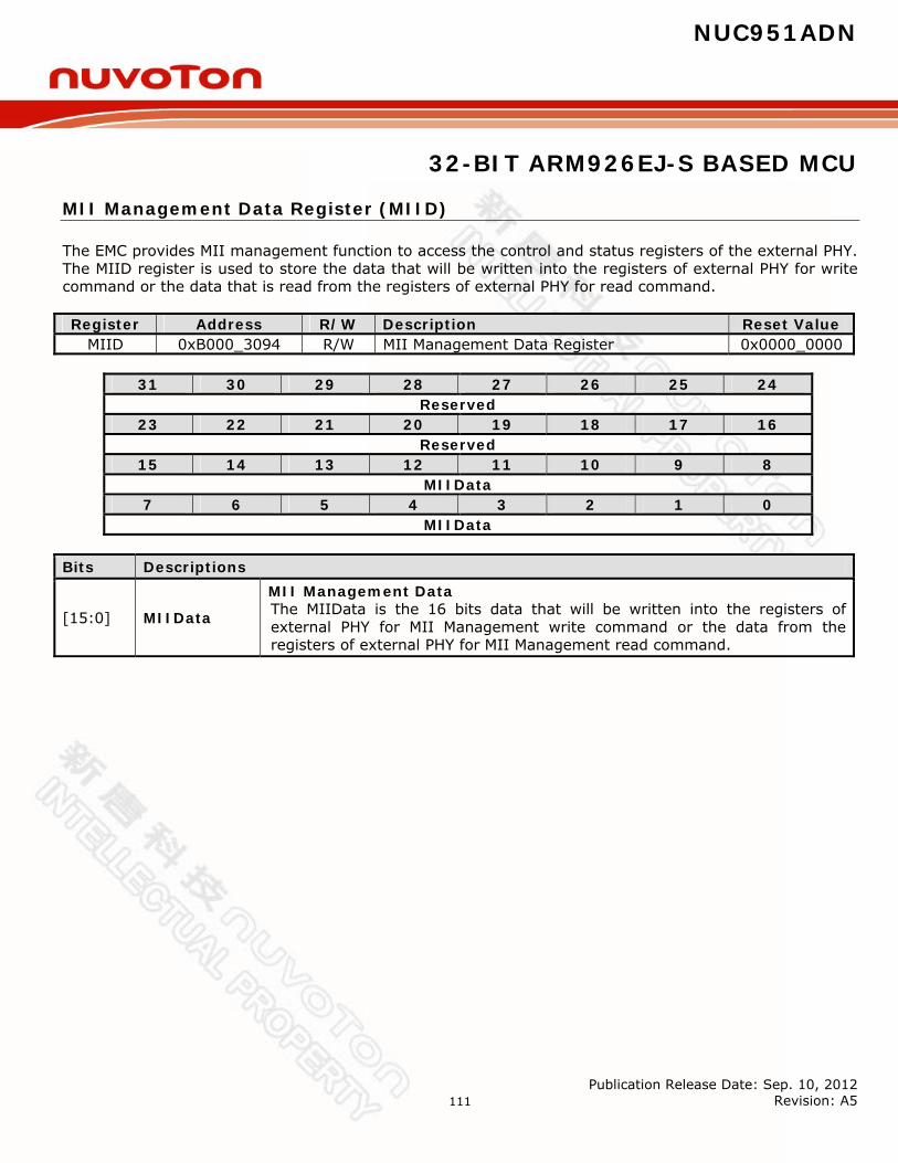
NUC951ADN
32-BIT ARM926EJ-S BASED MCU
Publication Release Date: Sep. 10, 2012 Revision: A5
111
MII Management Data Register (MIID)
The EMC provides MII management function to access the control and status registers of the external PHY. The MIID register is used to store the data that will be written into the registers of external PHY for write command or the data that is read from the registers of external PHY for read command. Register Address R/W Description Reset Value
MIID 0xB000_3094 R/W MII Management Data Register 0x0000_0000
31 30 29 28 27 26 25 24 Reserved
23 22 21 20 19 18 17 16 Reserved
15 14 13 12 11 10 9 8 MIIData
7 6 5 4 3 2 1 0 MIIData
Bits Descriptions
[15:0] MIIData
MII Management Data The MIIData is the 16 bits data that will be written into the registers of external PHY for MII Management write command or the data from the registers of external PHY for MII Management read command.
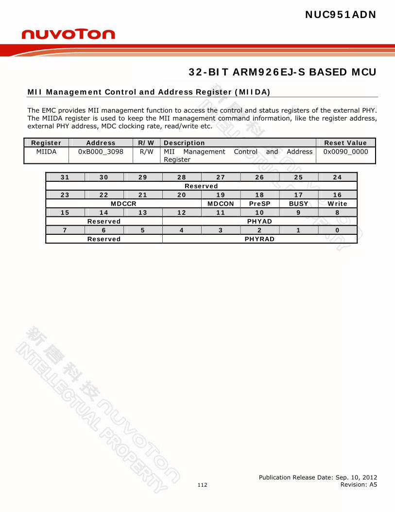
NUC951ADN
32-BIT ARM926EJ-S BASED MCU
Publication Release Date: Sep. 10, 2012 Revision: A5
112
MII Management Control and Address Register (MIIDA)
The EMC provides MII management function to access the control and status registers of the external PHY. The MIIDA register is used to keep the MII management command information, like the register address, external PHY address, MDC clocking rate, read/write etc. Register Address R/W Description Reset Value
MIIDA 0xB000_3098 R/W MII Management Control and Address Register
0x0090_0000
31 30 29 28 27 26 25 24
Reserved 23 22 21 20 19 18 17 16
MDCCR MDCON PreSP BUSY Write 15 14 13 12 11 10 9 8
Reserved PHYAD 7 6 5 4 3 2 1 0
Reserved PHYRAD

NUC951ADN
32-BIT ARM926EJ-S BASED MCU
Publication Release Date: Sep. 10, 2012 Revision: A5
113
Bits Descriptions
[23:20] MDCCR
MDC Clock Rating (Default Value: 4’h9) The MDCCR controls the MDC clock rating for MII Management I/F. Depend on the IEEE Std. 802.3 clause 22.2.2.11, the minimum period for MDC shall be 400ns. In other words, the maximum frequency for MDC is 2.5MHz. The MDC is divided from the AHB bus clock, the HCLK. Consequently, for different HCLKs the different ratios are required to generate appropriate MDC clock. The following table shows relationship between HCLK and MDC clock in different MDCCR configurations. The THCLK indicates the period of HCLK.
MDCCR [23:20]
MDC Clock Period MDC Clock Frequency
4’b0000 4 x THCLK HCLK/4 4’b0001 6 x THCLK HCLK/6 4’b0010 8 x THCLK HCLK/8 4’b0011 12 x THCLK HCLK/12 4’b0100 16 x THCLK HCLK/16 4’b0101 20 x THCLK HCLK/20 4’b0110 24 x THCLK HCLK/24 4’b0111 28 x THCLK HCLK/28 4’b1000 30 x THCLK HCLK/30 4’b1001 32 x THCLK HCLK/32 4’b1010 36 x THCLK HCLK/36 4’b1011 40 x THCLK HCLK/40 4’b1100 44 x THCLK HCLK/44 4’b1101 48 x THCLK HCLK/48 4’b1110 54 x THCLK HCLK/54 4’b1111 60 x THCLK HCLK/60
[19] MDCON
MDC Clock ON Always The MDC controls the MDC clock generation. If the MDCON is set to high, the MDC clock actives always. Otherwise, the MDC will only active while S/W issues a MII management command. 1’b0: The MDC clock will only active while S/W issues a MII management
command. 1’b1: The MDC clock actives always.
[18] PreSP
Preamble Suppress The PreSP controls the preamble field generation of MII management frame. If the PreSP is set to high, the preamble field generation of MII management frame is skipped. 1’b0: Preamble field generation of MII management frame is not skipped. 1’b1: Preamble field generation of MII management frame is skipped.
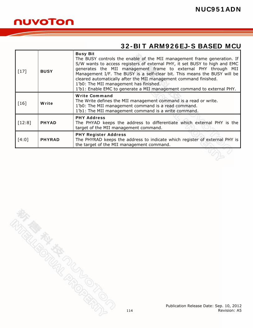
NUC951ADN
32-BIT ARM926EJ-S BASED MCU
Publication Release Date: Sep. 10, 2012 Revision: A5
114
[17] BUSY
Busy Bit The BUSY controls the enable of the MII management frame generation. If S/W wants to access registers of external PHY, it set BUSY to high and EMC generates the MII management frame to external PHY through MII Management I/F. The BUSY is a self-clear bit. This means the BUSY will be cleared automatically after the MII management command finished. 1’b0: The MII management has finished. 1’b1: Enable EMC to generate a MII management command to external PHY.
[16] Write
Write Command The Write defines the MII management command is a read or write. 1’b0: The MII management command is a read command. 1’b1: The MII management command is a write command.
[12:8] PHYAD PHY Address The PHYAD keeps the address to differentiate which external PHY is the target of the MII management command.
[4:0] PHYRAD PHY Register Address The PHYRAD keeps the address to indicate which register of external PHY is the target of the MII management command.

NUC951ADN
32-BIT ARM926EJ-S BASED MCU
Publication Release Date: Sep. 10, 2012 Revision: A5
115
MII Management Function Frame Format In IEEE Std. 802.3 clause 22.2.4, the MII management function is defined. The MII management function is used for the purpose of controlling the PHY and gathering status from the PHY. The MII management frame format is shown as follow.
Management frame fields PRE ST OP PHYAD REGAD TA DATA IDLE READ 1…1 01 10 AAAAA RRRRR Z0 DDDDDDDDDDDDDDDD Z WRITE 1…1 01 01 AAAAA RRRRR 10 DDDDDDDDDDDDDDDD Z MII Management Function Configure Sequence
Read Write 1. Set appropriate MDCCR. 2. Set PHYAD and PHYRAD. 3. Set Write to 1’b0 4. Set bit BUSY to 1’b1 to send a MII
management frame out. 5. Wait BUSY to become 1’b0. 6. Read data from MIID register. 7. Finish the read command.
1. Write data to MIID register 2. Set appropriate MDCCR. 3. Set PHYAD and PHYRAD. 4. Set Write to 1’b1 5. Set bit BUSY to 1’b1 to send a
MII management frame out. 6. Wait BUSY to become 1’b0. 7. Finish the write command.
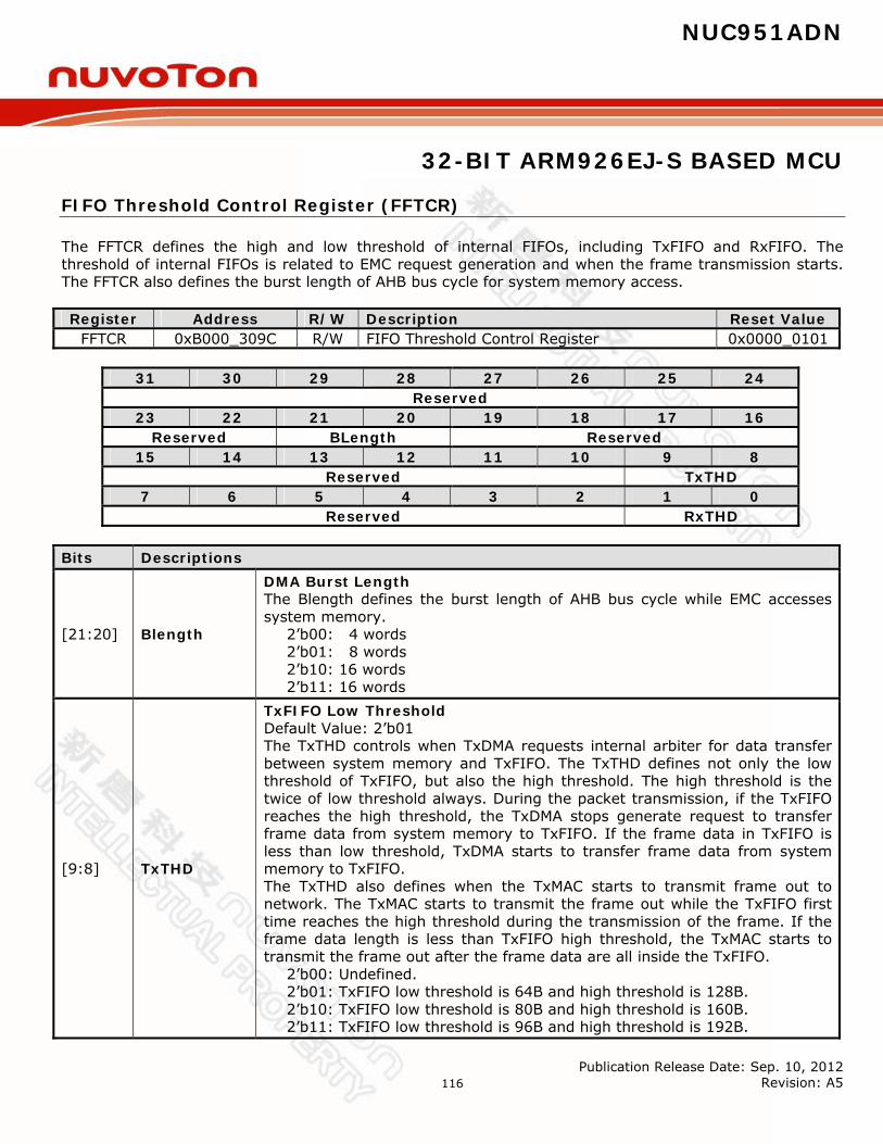
NUC951ADN
32-BIT ARM926EJ-S BASED MCU
Publication Release Date: Sep. 10, 2012 Revision: A5
116
FIFO Threshold Control Register (FFTCR)
The FFTCR defines the high and low threshold of internal FIFOs, including TxFIFO and RxFIFO. The threshold of internal FIFOs is related to EMC request generation and when the frame transmission starts. The FFTCR also defines the burst length of AHB bus cycle for system memory access. Register Address R/W Description Reset Value
FFTCR 0xB000_309C R/W FIFO Threshold Control Register 0x0000_0101
31 30 29 28 27 26 25 24 Reserved
23 22 21 20 19 18 17 16 Reserved BLength Reserved
15 14 13 12 11 10 9 8 Reserved TxTHD
7 6 5 4 3 2 1 0 Reserved RxTHD
Bits Descriptions
[21:20] Blength
DMA Burst Length The Blength defines the burst length of AHB bus cycle while EMC accesses system memory.
2’b00: 4 words 2’b01: 8 words 2’b10: 16 words 2’b11: 16 words
[9:8] TxTHD
TxFIFO Low Threshold Default Value: 2’b01 The TxTHD controls when TxDMA requests internal arbiter for data transfer between system memory and TxFIFO. The TxTHD defines not only the low threshold of TxFIFO, but also the high threshold. The high threshold is the twice of low threshold always. During the packet transmission, if the TxFIFO reaches the high threshold, the TxDMA stops generate request to transfer frame data from system memory to TxFIFO. If the frame data in TxFIFO is less than low threshold, TxDMA starts to transfer frame data from system memory to TxFIFO. The TxTHD also defines when the TxMAC starts to transmit frame out to network. The TxMAC starts to transmit the frame out while the TxFIFO first time reaches the high threshold during the transmission of the frame. If the frame data length is less than TxFIFO high threshold, the TxMAC starts to transmit the frame out after the frame data are all inside the TxFIFO.
2’b00: Undefined. 2’b01: TxFIFO low threshold is 64B and high threshold is 128B. 2’b10: TxFIFO low threshold is 80B and high threshold is 160B. 2’b11: TxFIFO low threshold is 96B and high threshold is 192B.
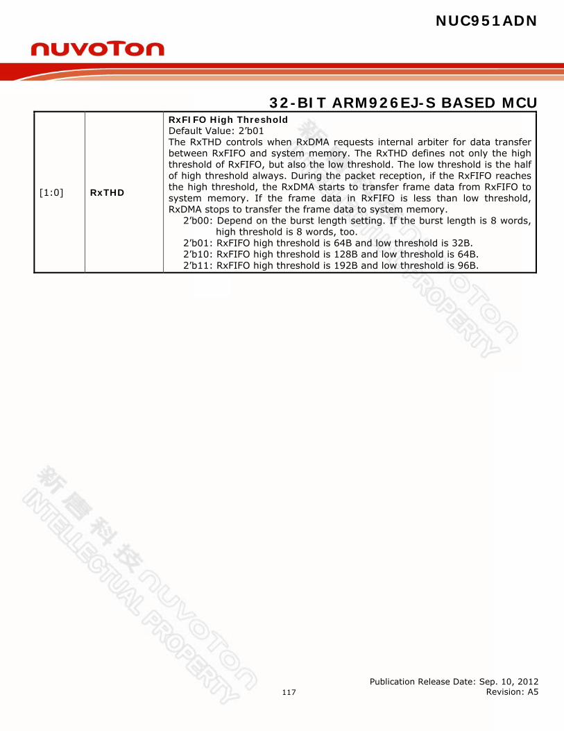
NUC951ADN
32-BIT ARM926EJ-S BASED MCU
Publication Release Date: Sep. 10, 2012 Revision: A5
117
[1:0] RxTHD
RxFIFO High Threshold Default Value: 2’b01 The RxTHD controls when RxDMA requests internal arbiter for data transfer between RxFIFO and system memory. The RxTHD defines not only the high threshold of RxFIFO, but also the low threshold. The low threshold is the half of high threshold always. During the packet reception, if the RxFIFO reaches the high threshold, the RxDMA starts to transfer frame data from RxFIFO to system memory. If the frame data in RxFIFO is less than low threshold, RxDMA stops to transfer the frame data to system memory.
2’b00: Depend on the burst length setting. If the burst length is 8 words, high threshold is 8 words, too.
2’b01: RxFIFO high threshold is 64B and low threshold is 32B. 2’b10: RxFIFO high threshold is 128B and low threshold is 64B. 2’b11: RxFIFO high threshold is 192B and low threshold is 96B.

NUC951ADN
32-BIT ARM926EJ-S BASED MCU
Publication Release Date: Sep. 10, 2012 Revision: A5
118
Transmit Start Demand Register (TSDR)
If the Tx descriptor is not available for use of TxDMA after the TXON of MCMDR register is enabled, the FSM (Finite State Machine) of TxDMA enters the Halt state and the frame transmission is halted. After the S/W has prepared the new Tx descriptor for frame transmission, it must issue a write command to TSDR register to make TxDMA leave Halt state and contiguous frame transmission. The TSDR is a write only register and read from this register is undefined. The write to TSDR register has took effect only while TxDMA stayed at Halt state. Register Address R/W Description Reset Value
TSDR 0xB000_30A0 W Transmit Start Demand Register Undefined
31 30 29 28 27 26 25 24 TSD
23 22 21 20 19 18 17 16 TSD
15 14 13 12 11 10 9 8 TSD
7 6 5 4 3 2 1 0 TSD
Bits Descriptions [31:0] TSD Transmit Start Demand
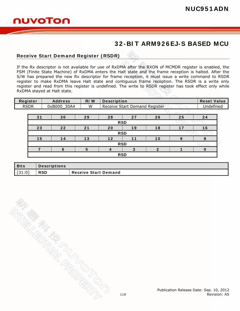
NUC951ADN
32-BIT ARM926EJ-S BASED MCU
Publication Release Date: Sep. 10, 2012 Revision: A5
119
Receive Start Demand Register (RSDR)
If the Rx descriptor is not available for use of RxDMA after the RXON of MCMDR register is enabled, the FSM (Finite State Machine) of RxDMA enters the Halt state and the frame reception is halted. After the S/W has prepared the new Rx descriptor for frame reception, it must issue a write command to RSDR register to make RxDMA leave Halt state and contiguous frame reception. The RSDR is a write only register and read from this register is undefined. The write to RSDR register has took effect only while RxDMA stayed at Halt state. Register Address R/W Description Reset Value
RSDR 0xB000_30A4 W Receive Start Demand Register Undefined
31 30 29 28 27 26 25 24 RSD
23 22 21 20 19 18 17 16 RSD
15 14 13 12 11 10 9 8 RSD
7 6 5 4 3 2 1 0 RSD
Bits Descriptions [31:0] RSD Receive Start Demand

NUC951ADN
32-BIT ARM926EJ-S BASED MCU
Publication Release Date: Sep. 10, 2012 Revision: A5
120
Maximum Receive Frame Control Register (DMARFC)
The DMARFC defines the maximum frame length for a received frame that can be stored in the system memory. It is recommend that only use this register while S/W wants to receive a frame which length is greater than 1518 bytes. Register Address R/W Description Reset Value DMARFC 0xB000_30A8 R/W Maximum Receive Frame Control Register 0x0000_0800
31 30 29 28 27 26 25 24
Reserved 23 22 21 20 19 18 17 16
Reserved 15 14 13 12 11 10 9 8
RXMS 7 6 5 4 3 2 1 0
RXMS Bits Descriptions
[15:0] RXMS
Maximum Receive Frame Length Default Value: 16’h0800 The RXMS defines the maximum frame length for received frame. If the frame length of received frame is greater than RXMS, and bit EnDFO of MIEN register is also enabled, the bit DFOI of MISTA register is set and the Rx interrupt is triggered. It is recommended that only use RXMS to qualify the length of received frame while S/W wants to receive a frame which length is greater than 1518 bytes.
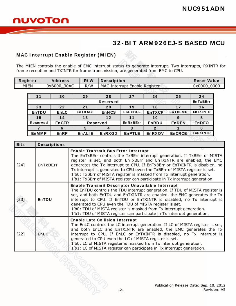
NUC951ADN
32-BIT ARM926EJ-S BASED MCU
Publication Release Date: Sep. 10, 2012 Revision: A5
121
MAC Interrupt Enable Register (MIEN)
The MIEN controls the enable of EMC interrupt status to generate interrupt. Two interrupts, RXINTR for frame reception and TXINTR for frame transmission, are generated from EMC to CPU. Register Address R/W Description Reset Value
MIEN 0xB000_30AC R/W MAC Interrupt Enable Register 0x0000_0000
31 30 29 28 27 26 25 24 Reserved EnTxBErr
23 22 21 20 19 18 17 16 EnTDU EnLC EnTXABT EnNCS EnEXDEF EnTXCP EnTXEMP EnTXINTR
15 14 13 12 11 10 9 8 Reserved EnCFR Reserved EnRxBErr EnRDU EnDEN EnDFO
7 6 5 4 3 2 1 0 EnMMP EnRP EnALIE EnRXGD EnPTLE EnRXOV EnCRCE EnRXINTR
Bits Descriptions
[24] EnTxBErr
Enable Transmit Bus Error Interrupt The EnTxBErr controls the TxBErr interrupt generation. If TxBErr of MISTA register is set, and both EnTxBErr and EnTXINTR are enabled, the EMC generates the Tx interrupt to CPU. If EnTxBErr or EnTXINTR is disabled, no Tx interrupt is generated to CPU even the TxBErr of MISTA register is set. 1’b0: TxBErr of MISTA register is masked from Tx interrupt generation. 1’b1: TxBErr of MISTA register can participate in Tx interrupt generation.
[23] EnTDU
Enable Transmit Descriptor Unavailable Interrupt The EnTDU controls the TDU interrupt generation. If TDU of MISTA register is set, and both EnTDU and EnTXINTR are enabled, the EMC generates the Tx interrupt to CPU. If EnTDU or EnTXINTR is disabled, no Tx interrupt is generated to CPU even the TDU of MISTA register is set. 1’b0: TDU of MISTA register is masked from Tx interrupt generation. 1’b1: TDU of MISTA register can participate in Tx interrupt generation.
[22] EnLC
Enable Late Collision Interrupt The EnLC controls the LC interrupt generation. If LC of MISTA register is set, and both EnLC and EnTXINTR are enabled, the EMC generates the Tx interrupt to CPU. If EnLC or EnTXINTR is disabled, no Tx interrupt is generated to CPU even the LC of MISTA register is set. 1’b0: LC of MISTA register is masked from Tx interrupt generation. 1’b1: LC of MISTA register can participate in Tx interrupt generation.
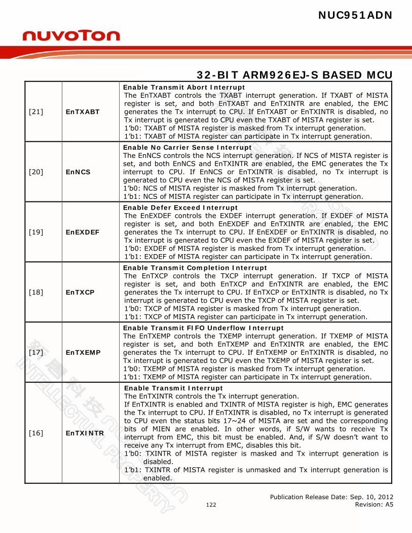
NUC951ADN
32-BIT ARM926EJ-S BASED MCU
Publication Release Date: Sep. 10, 2012 Revision: A5
122
[21] EnTXABT
Enable Transmit Abort Interrupt The EnTXABT controls the TXABT interrupt generation. If TXABT of MISTA register is set, and both EnTXABT and EnTXINTR are enabled, the EMC generates the Tx interrupt to CPU. If EnTXABT or EnTXINTR is disabled, no Tx interrupt is generated to CPU even the TXABT of MISTA register is set. 1’b0: TXABT of MISTA register is masked from Tx interrupt generation. 1’b1: TXABT of MISTA register can participate in Tx interrupt generation.
[20] EnNCS
Enable No Carrier Sense Interrupt The EnNCS controls the NCS interrupt generation. If NCS of MISTA register is set, and both EnNCS and EnTXINTR are enabled, the EMC generates the Tx interrupt to CPU. If EnNCS or EnTXINTR is disabled, no Tx interrupt is generated to CPU even the NCS of MISTA register is set. 1’b0: NCS of MISTA register is masked from Tx interrupt generation. 1’b1: NCS of MISTA register can participate in Tx interrupt generation.
[19] EnEXDEF
Enable Defer Exceed Interrupt The EnEXDEF controls the EXDEF interrupt generation. If EXDEF of MISTA register is set, and both EnEXDEF and EnTXINTR are enabled, the EMC generates the Tx interrupt to CPU. If EnEXDEF or EnTXINTR is disabled, no Tx interrupt is generated to CPU even the EXDEF of MISTA register is set. 1’b0: EXDEF of MISTA register is masked from Tx interrupt generation. 1’b1: EXDEF of MISTA register can participate in Tx interrupt generation.
[18] EnTXCP
Enable Transmit Completion Interrupt The EnTXCP controls the TXCP interrupt generation. If TXCP of MISTA register is set, and both EnTXCP and EnTXINTR are enabled, the EMC generates the Tx interrupt to CPU. If EnTXCP or EnTXINTR is disabled, no Tx interrupt is generated to CPU even the TXCP of MISTA register is set. 1’b0: TXCP of MISTA register is masked from Tx interrupt generation. 1’b1: TXCP of MISTA register can participate in Tx interrupt generation.
[17] EnTXEMP
Enable Transmit FIFO Underflow Interrupt The EnTXEMP controls the TXEMP interrupt generation. If TXEMP of MISTA register is set, and both EnTXEMP and EnTXINTR are enabled, the EMC generates the Tx interrupt to CPU. If EnTXEMP or EnTXINTR is disabled, no Tx interrupt is generated to CPU even the TXEMP of MISTA register is set. 1’b0: TXEMP of MISTA register is masked from Tx interrupt generation. 1’b1: TXEMP of MISTA register can participate in Tx interrupt generation.
[16] EnTXINTR
Enable Transmit Interrupt The EnTXINTR controls the Tx interrupt generation. If EnTXINTR is enabled and TXINTR of MISTA register is high, EMC generates the Tx interrupt to CPU. If EnTXINTR is disabled, no Tx interrupt is generated to CPU even the status bits 17~24 of MISTA are set and the corresponding bits of MIEN are enabled. In other words, if S/W wants to receive Tx interrupt from EMC, this bit must be enabled. And, if S/W doesn’t want to receive any Tx interrupt from EMC, disables this bit. 1’b0: TXINTR of MISTA register is masked and Tx interrupt generation is
disabled. 1’b1: TXINTR of MISTA register is unmasked and Tx interrupt generation is
enabled.
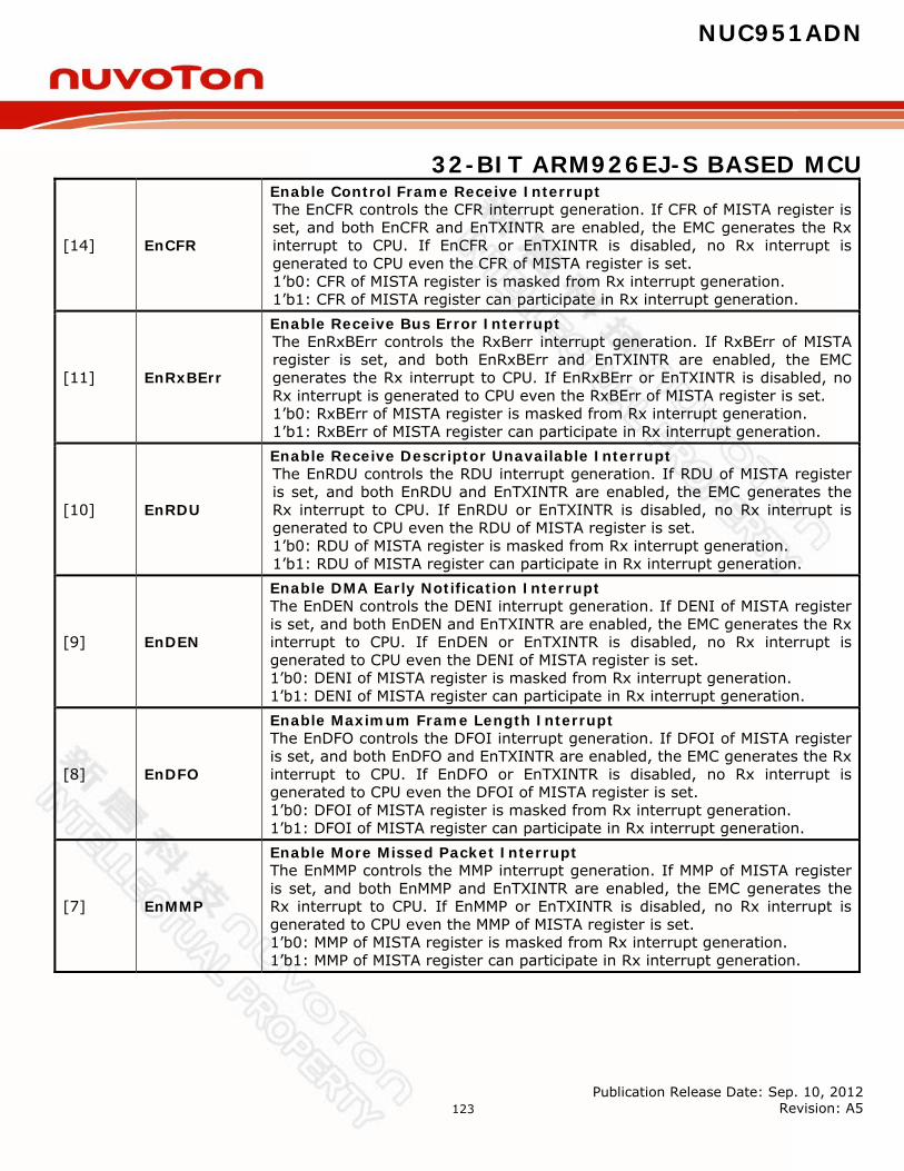
NUC951ADN
32-BIT ARM926EJ-S BASED MCU
Publication Release Date: Sep. 10, 2012 Revision: A5
123
[14] EnCFR
Enable Control Frame Receive Interrupt The EnCFR controls the CFR interrupt generation. If CFR of MISTA register is set, and both EnCFR and EnTXINTR are enabled, the EMC generates the Rx interrupt to CPU. If EnCFR or EnTXINTR is disabled, no Rx interrupt is generated to CPU even the CFR of MISTA register is set. 1’b0: CFR of MISTA register is masked from Rx interrupt generation. 1’b1: CFR of MISTA register can participate in Rx interrupt generation.
[11] EnRxBErr
Enable Receive Bus Error Interrupt The EnRxBErr controls the RxBerr interrupt generation. If RxBErr of MISTA register is set, and both EnRxBErr and EnTXINTR are enabled, the EMC generates the Rx interrupt to CPU. If EnRxBErr or EnTXINTR is disabled, no Rx interrupt is generated to CPU even the RxBErr of MISTA register is set. 1’b0: RxBErr of MISTA register is masked from Rx interrupt generation. 1’b1: RxBErr of MISTA register can participate in Rx interrupt generation.
[10] EnRDU
Enable Receive Descriptor Unavailable Interrupt The EnRDU controls the RDU interrupt generation. If RDU of MISTA register is set, and both EnRDU and EnTXINTR are enabled, the EMC generates the Rx interrupt to CPU. If EnRDU or EnTXINTR is disabled, no Rx interrupt is generated to CPU even the RDU of MISTA register is set. 1’b0: RDU of MISTA register is masked from Rx interrupt generation. 1’b1: RDU of MISTA register can participate in Rx interrupt generation.
[9] EnDEN
Enable DMA Early Notification Interrupt The EnDEN controls the DENI interrupt generation. If DENI of MISTA register is set, and both EnDEN and EnTXINTR are enabled, the EMC generates the Rx interrupt to CPU. If EnDEN or EnTXINTR is disabled, no Rx interrupt is generated to CPU even the DENI of MISTA register is set. 1’b0: DENI of MISTA register is masked from Rx interrupt generation. 1’b1: DENI of MISTA register can participate in Rx interrupt generation.
[8] EnDFO
Enable Maximum Frame Length Interrupt The EnDFO controls the DFOI interrupt generation. If DFOI of MISTA register is set, and both EnDFO and EnTXINTR are enabled, the EMC generates the Rx interrupt to CPU. If EnDFO or EnTXINTR is disabled, no Rx interrupt is generated to CPU even the DFOI of MISTA register is set. 1’b0: DFOI of MISTA register is masked from Rx interrupt generation. 1’b1: DFOI of MISTA register can participate in Rx interrupt generation.
[7] EnMMP
Enable More Missed Packet Interrupt The EnMMP controls the MMP interrupt generation. If MMP of MISTA register is set, and both EnMMP and EnTXINTR are enabled, the EMC generates the Rx interrupt to CPU. If EnMMP or EnTXINTR is disabled, no Rx interrupt is generated to CPU even the MMP of MISTA register is set. 1’b0: MMP of MISTA register is masked from Rx interrupt generation. 1’b1: MMP of MISTA register can participate in Rx interrupt generation.
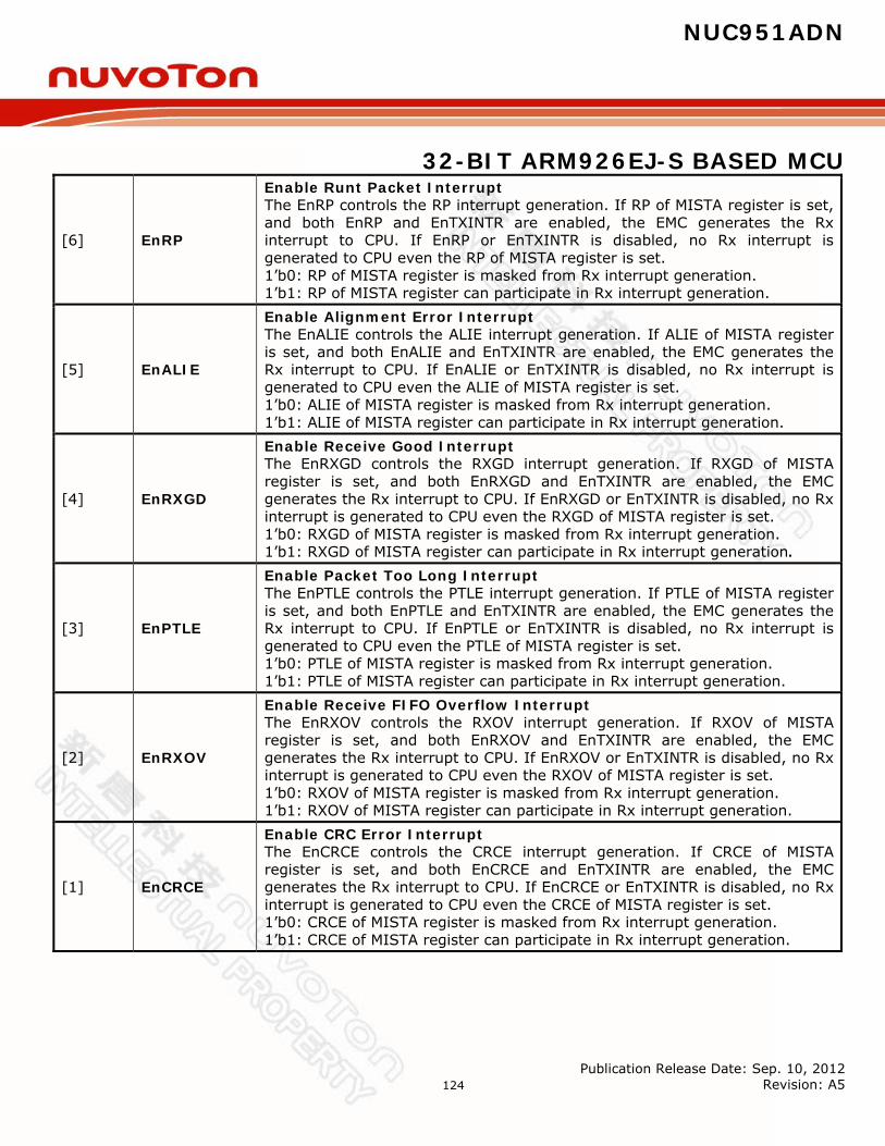
NUC951ADN
32-BIT ARM926EJ-S BASED MCU
Publication Release Date: Sep. 10, 2012 Revision: A5
124
[6] EnRP
Enable Runt Packet Interrupt The EnRP controls the RP interrupt generation. If RP of MISTA register is set, and both EnRP and EnTXINTR are enabled, the EMC generates the Rx interrupt to CPU. If EnRP or EnTXINTR is disabled, no Rx interrupt is generated to CPU even the RP of MISTA register is set. 1’b0: RP of MISTA register is masked from Rx interrupt generation. 1’b1: RP of MISTA register can participate in Rx interrupt generation.
[5] EnALIE
Enable Alignment Error Interrupt The EnALIE controls the ALIE interrupt generation. If ALIE of MISTA register is set, and both EnALIE and EnTXINTR are enabled, the EMC generates the Rx interrupt to CPU. If EnALIE or EnTXINTR is disabled, no Rx interrupt is generated to CPU even the ALIE of MISTA register is set. 1’b0: ALIE of MISTA register is masked from Rx interrupt generation. 1’b1: ALIE of MISTA register can participate in Rx interrupt generation.
[4] EnRXGD
Enable Receive Good Interrupt The EnRXGD controls the RXGD interrupt generation. If RXGD of MISTA register is set, and both EnRXGD and EnTXINTR are enabled, the EMC generates the Rx interrupt to CPU. If EnRXGD or EnTXINTR is disabled, no Rx interrupt is generated to CPU even the RXGD of MISTA register is set. 1’b0: RXGD of MISTA register is masked from Rx interrupt generation. 1’b1: RXGD of MISTA register can participate in Rx interrupt generation.
[3] EnPTLE
Enable Packet Too Long Interrupt The EnPTLE controls the PTLE interrupt generation. If PTLE of MISTA register is set, and both EnPTLE and EnTXINTR are enabled, the EMC generates the Rx interrupt to CPU. If EnPTLE or EnTXINTR is disabled, no Rx interrupt is generated to CPU even the PTLE of MISTA register is set. 1’b0: PTLE of MISTA register is masked from Rx interrupt generation. 1’b1: PTLE of MISTA register can participate in Rx interrupt generation.
[2] EnRXOV
Enable Receive FIFO Overflow Interrupt The EnRXOV controls the RXOV interrupt generation. If RXOV of MISTA register is set, and both EnRXOV and EnTXINTR are enabled, the EMC generates the Rx interrupt to CPU. If EnRXOV or EnTXINTR is disabled, no Rx interrupt is generated to CPU even the RXOV of MISTA register is set. 1’b0: RXOV of MISTA register is masked from Rx interrupt generation. 1’b1: RXOV of MISTA register can participate in Rx interrupt generation.
[1] EnCRCE
Enable CRC Error Interrupt The EnCRCE controls the CRCE interrupt generation. If CRCE of MISTA register is set, and both EnCRCE and EnTXINTR are enabled, the EMC generates the Rx interrupt to CPU. If EnCRCE or EnTXINTR is disabled, no Rx interrupt is generated to CPU even the CRCE of MISTA register is set. 1’b0: CRCE of MISTA register is masked from Rx interrupt generation. 1’b1: CRCE of MISTA register can participate in Rx interrupt generation.
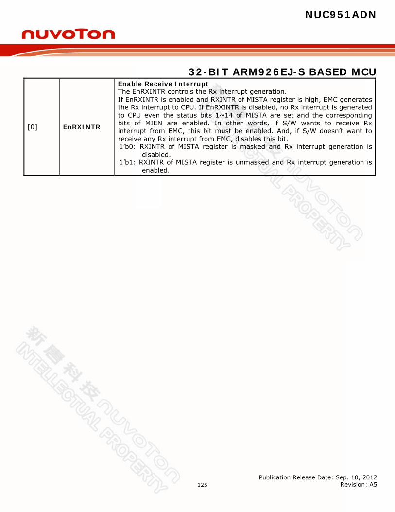
NUC951ADN
32-BIT ARM926EJ-S BASED MCU
Publication Release Date: Sep. 10, 2012 Revision: A5
125
[0] EnRXINTR
Enable Receive Interrupt The EnRXINTR controls the Rx interrupt generation. If EnRXINTR is enabled and RXINTR of MISTA register is high, EMC generates the Rx interrupt to CPU. If EnRXINTR is disabled, no Rx interrupt is generated to CPU even the status bits 1~14 of MISTA are set and the corresponding bits of MIEN are enabled. In other words, if S/W wants to receive Rx interrupt from EMC, this bit must be enabled. And, if S/W doesn’t want to receive any Rx interrupt from EMC, disables this bit. 1’b0: RXINTR of MISTA register is masked and Rx interrupt generation is
disabled. 1’b1: RXINTR of MISTA register is unmasked and Rx interrupt generation is
enabled.

NUC951ADN
32-BIT ARM926EJ-S BASED MCU
Publication Release Date: Sep. 10, 2012 Revision: A5
126
MAC Interrupt Status Register (MISTA)
The MISTA keeps much EMC statuses, like frame transmission and reception status, internal FIFO status and also NATA processing status. The statuses kept in MISTA will trigger the reception or transmission interrupt. The MISTA is a write clear register and write 1 to corresponding bit clears the status and also clears the interrupt. Register Address R/W Description Reset Value
MISTA 0xB000_30B0 R/W MAC Interrupt Status Register 0x0000_0000
31 30 29 28 27 26 25 24 Reserved TxBErr
23 22 21 20 19 18 17 16 TDU LC TXABT NCS EXDEF TXCP TXEMP TXINTR 15 14 13 12 11 10 9 8
Reserved CFR Reserved RxBErr RDU DENI DFOI 7 6 5 4 3 2 1 0
MMP RP ALIE RXGD PTLE RXOV CRCE RXINTR Bits Descriptions
[24] TxBErr
Transmit Bus Error Interrupt The TxBErr high indicates the memory controller replies ERROR response while EMC access system memory through TxDMA during packet transmission process. Reset EMC is recommended while TxBErr status is high. If the TxBErr is high and EnTxBErr of MIEN register is enabled, the TxINTR will be high. Write 1 to this bit clears the TxBErr status. 1’b0: No ERROR response is received. 1’b1: ERROR response is received.
[23] TDU
Transmit Descriptor Unavailable Interrupt The TDU high indicates that there is no available Tx descriptor for packet transmission and TxDMA will stay at Halt state. Once, the TxDMA enters the Halt state, S/W must issues a write command to TSDR register to make TxDMA leave Halt state while new Tx descriptor is available. If the TDU is high and EnTDU of MIEN register is enabled, the TxINTR will be high. Write 1 to this bit clears the TDU status. 1’b0: Tx descriptor is available. 1’b1: Tx descriptor is unavailable.

NUC951ADN
32-BIT ARM926EJ-S BASED MCU
Publication Release Date: Sep. 10, 2012 Revision: A5
127
[22] LC
Late Collision Interrupt The LC high indicates the collision occurred in the outside of 64 bytes collision window. This means after the 64 bytes of a frame has transmitted out to the network, the collision still occurred. The late collision check will only be done while EMC is operating on half-duplex mode. If the LC is high and EnLC of MIEN register is enabled, the TxINTR will be high. Write 1 to this bit clears the LC status. 1’b0: No collision occurred in the outside of 64 bytes collision window. 1’b1: Collision occurred in the outside of 64 bytes collision window.
[21] TXABT
Transmit Abort Interrupt The TXABT high indicates the packet incurred 16 consecutive collisions during transmission, and then the transmission process for this packet is aborted. The transmission abort is only available while EMC is operating on half-duplex mode. If the TXABT is high and EnTXABT of MIEN register is enabled, the TxINTR will be high. Write 1 to this bit clears the TXABT status. 1’b0: Packet doesn’t incur 16 consecutive collisions during transmission. 1’b1: Packet incurred 16 consecutive collisions during transmission.
[20] NCS
No Carrier Sense Interrupt The NCS high indicates the MII I/F signal CRS doesn’t active at the start of or during the packet transmission. The NCS is only available while EMC is operating on half-duplex mode. If the NCS is high and EnNCS of MIEN register is enabled, the TxINTR will be high. Write 1 to this bit clears the NCS status. 1’b0: CRS signal actives correctly. 1’b1: CRS signal doesn’t active at the start of or during the packet transmission.
[19] EXDEF
Defer Exceed Interrupt The EXDEF high indicates the frame waiting for transmission has deferred over 0.32768ms on 100Mbps mode, or 3.2768ms on 10Mbps mode. The deferral exceed check will only be done while bit NDEF of MCMDR is disabled, and EMC is operating on half-duplex mode. If the EXDEF is high and EnEXDEF of MIEN register is enabled, the TxINTR will be high. Write 1 to this bit clears the EXDEF status. 1’b0: Frame waiting for transmission has not deferred over 0.32768ms
(100Mbps) or 3.2768ms (10Mbps). 1’b1: Frame waiting for transmission has deferred over 0.32768ms
(100Mbps) or 3.2768ms (10Mbps).
[18] TXCP
Transmit Completion Interrupt The TXCP indicates the packet transmission has completed correctly. If the TXCP is high and EnTXCP of MIEN register is enabled, the TxINTR will be high. Write 1 to this bit clears the TXCP status. 1’b0: The packet transmission doesn’t complete. 1’b1: The packet transmission has completed.

NUC951ADN
32-BIT ARM926EJ-S BASED MCU
Publication Release Date: Sep. 10, 2012 Revision: A5
128
[17] TXEMP
Transmit FIFO Underflow Interrupt The TXEMP high indicates the TxFIFO underflow occurred during packet transmission. While the TxFIFO underflow occurred, the EMC will retransmit the packet automatically without S/W intervention. If the TxFIFO underflow occurred often, it is recommended that modify TxFIFO threshold control, the TxTHD of FFTCR register, to higher level. If the TXEMP is high and EnTXEMP of MIEN register is enabled, the TxINTR will be high. Write 1 to this bit clears the TXEMP status. 1’b0: No TxFIFO underflow occurred during packet transmission. 1’b0: TxFIFO underflow occurred during packet transmission.
[16] TXINTR
Transmit Interrupt The TXINTR indicates the Tx interrupt status. If TXINTR high and its corresponding enable bit, EnTXINTR of MISTA register, is also high indicates the EMC generates Tx interrupt to CPU. If TXINTR is high but EnTXINTR of MISTA is disabled, no Tx interrupt is generated. The TXINTR is a logic OR result of the bits 17~24 in MISTA register do logic AND with the corresponding bits in MIEN register. In other words, if one of the bits 17~24 in MISTA register is high and its corresponding enable bit in MIEN register is also enabled, the TXINTR will be high. Because the TXINTR is a logic OR result, clears bits 17~24 of MISTA register makes TXINTR be cleared, too. 1’b0: No status of bits 17~24 in MISTA is set or no enable of bits 17~24 in
MIEN is turned on. 1’b1: At least one status of bits 17~24 in MISTA is set and its corresponding
enable bit is turned on.
[14] CFR
Control Frame Receive Interrupt The CFR high indicates EMC receives a flow control frame. The CFR only available while EMC is operating on full duplex mode. If the CFR is high and EnCFR of MIEN register is enabled, the RxINTR will be high. Write 1 to this bit clears the CFR status. 1’b0: The EMC doesn’t receive the flow control frame. 1’b1: The EMC receives a flow control frame.
[11] RxBErr
Receive Bus Error Interrupt The RxBErr high indicates the memory controller replies ERROR response while EMC access system memory through RxDMA during packet reception process. Reset EMC is recommended while RxBErr status is high. If the RxBErr is high and EnRxBErr of MIEN register is enabled, the RxINTR will be high. Write 1 to this bit clears the RxBErr status. 1’b0: No ERROR response is received. 1’b1: ERROR response is received.
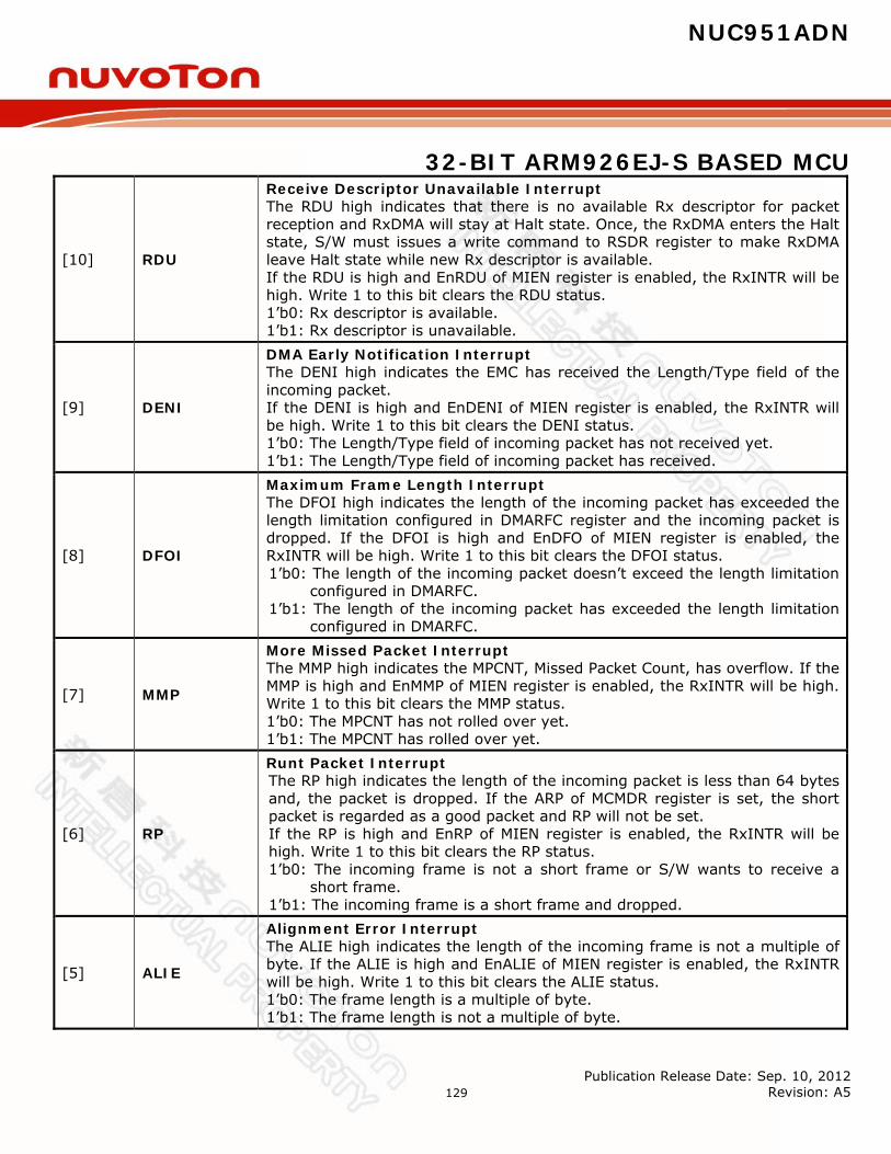
NUC951ADN
32-BIT ARM926EJ-S BASED MCU
Publication Release Date: Sep. 10, 2012 Revision: A5
129
[10] RDU
Receive Descriptor Unavailable Interrupt The RDU high indicates that there is no available Rx descriptor for packet reception and RxDMA will stay at Halt state. Once, the RxDMA enters the Halt state, S/W must issues a write command to RSDR register to make RxDMA leave Halt state while new Rx descriptor is available. If the RDU is high and EnRDU of MIEN register is enabled, the RxINTR will be high. Write 1 to this bit clears the RDU status. 1’b0: Rx descriptor is available. 1’b1: Rx descriptor is unavailable.
[9] DENI
DMA Early Notification Interrupt The DENI high indicates the EMC has received the Length/Type field of the incoming packet. If the DENI is high and EnDENI of MIEN register is enabled, the RxINTR will be high. Write 1 to this bit clears the DENI status. 1’b0: The Length/Type field of incoming packet has not received yet. 1’b1: The Length/Type field of incoming packet has received.
[8] DFOI
Maximum Frame Length Interrupt The DFOI high indicates the length of the incoming packet has exceeded the length limitation configured in DMARFC register and the incoming packet is dropped. If the DFOI is high and EnDFO of MIEN register is enabled, the RxINTR will be high. Write 1 to this bit clears the DFOI status. 1’b0: The length of the incoming packet doesn’t exceed the length limitation
configured in DMARFC. 1’b1: The length of the incoming packet has exceeded the length limitation
configured in DMARFC.
[7] MMP
More Missed Packet Interrupt The MMP high indicates the MPCNT, Missed Packet Count, has overflow. If the MMP is high and EnMMP of MIEN register is enabled, the RxINTR will be high. Write 1 to this bit clears the MMP status. 1’b0: The MPCNT has not rolled over yet. 1’b1: The MPCNT has rolled over yet.
[6] RP
Runt Packet Interrupt The RP high indicates the length of the incoming packet is less than 64 bytes and, the packet is dropped. If the ARP of MCMDR register is set, the short packet is regarded as a good packet and RP will not be set. If the RP is high and EnRP of MIEN register is enabled, the RxINTR will be high. Write 1 to this bit clears the RP status. 1’b0: The incoming frame is not a short frame or S/W wants to receive a
short frame. 1’b1: The incoming frame is a short frame and dropped.
[5] ALIE
Alignment Error Interrupt The ALIE high indicates the length of the incoming frame is not a multiple of byte. If the ALIE is high and EnALIE of MIEN register is enabled, the RxINTR will be high. Write 1 to this bit clears the ALIE status. 1’b0: The frame length is a multiple of byte. 1’b1: The frame length is not a multiple of byte.

NUC951ADN
32-BIT ARM926EJ-S BASED MCU
Publication Release Date: Sep. 10, 2012 Revision: A5
130
[4] RXGD
Receive Good Interrupt The RXGD high indicates the frame reception has completed. If the RXGD is high and EnRXGD of MIEN register is enabled, the RxINTR will be high. Write 1 to this bit clears the RXGD status. 1’b0: The frame reception has not complete yet. 1’b1: The frame reception has completed.
[3] PTLE
Packet Too Long Interrupt The PTLE high indicates the length of the incoming packet is greater than 1518 bytes and the incoming packet is dropped. If the ALP of MCMDR register is set, the long packet will be regarded as a good packet and PTLE will not be set. If the PTLE is high and EnPTLE of MIEN register is enabled, the RxINTR will be high. Write 1 to this bit clears the PTLE status. 1’b0: The incoming frame is not a long frame or S/W wants to receive a long frame. 1’b1: The incoming frame is a long frame and dropped.
[2] RXOV
Receive FIFO Overflow Interrupt The RXOV high indicates the RxFIFO overflow occurred during packet reception. While the RxFIFO overflow occurred, the EMC drops the current receiving packer. If the RxFIFO overflow occurred often, it is recommended that modify RxFIFO threshold control, the RxTHD of FFTCR register, to higher level. If the RXOV is high and EnRXOV of MIEN register is enabled, the RxINTR will be high. Write 1 to this bit clears the RXOV status. 1’b0: No RxFIFO overflow occurred during packet reception. 1’b0: RxFIFO overflow occurred during packet reception.
[1] CRCE
CRC Error Interrupt The CRCE high indicates the incoming packet incurred the CRC error and the packet is dropped. If the AEP of MCMDR register is set, the CRC error packet will be regarded as a good packet and CRCE will not be set. If the CRCE is high and EnCRCE of MIEN register is enabled, the RxINTR will be high. Write 1 to this bit clears the CRCE status. 1’b0: The frame doesn’t incur CRC error. 1’b1: The frame incurred CRC error.

NUC951ADN
32-BIT ARM926EJ-S BASED MCU
Publication Release Date: Sep. 10, 2012 Revision: A5
131
[0] RXINTR
Receive Interrupt The RXINTR indicates the Rx interrupt status. If RXINTR high and its corresponding enable bit, EnRXINTR of MISTA register, is also high indicates the EMC generates Rx interrupt to CPU. If RXINTR is high but EnRXINTR of MISTA is disabled, no Rx interrupt is generated. The RXINTR is a logic OR result of the bits 1~14 in MISTA register do logic AND with the corresponding bits in MIEN register. In other words, if one of the bits 1~14 in MISTA register is high and its corresponding enable bit in MIEN register is also enabled, the RXINTR will be high. Because the RXINTR is a logic OR result, clears bits 1~14 of MISTA register makes RXINTR be cleared, too. 1’b0: No status of bits 1~14 in MISTA is set or no enable of bits 1~14 in
MIEN is turned on. 1’b1: At least one status of bits 1~14 in MISTA is set and its corresponding
enable bit is turned on.
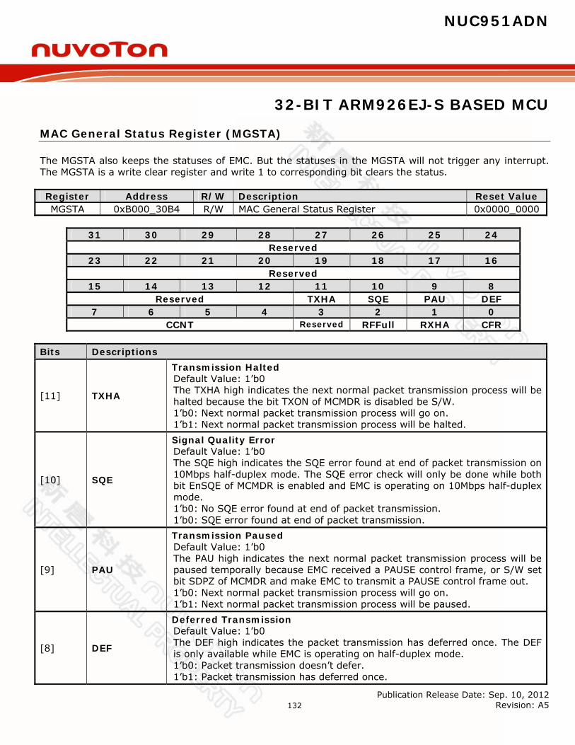
NUC951ADN
32-BIT ARM926EJ-S BASED MCU
Publication Release Date: Sep. 10, 2012 Revision: A5
132
MAC General Status Register (MGSTA)
The MGSTA also keeps the statuses of EMC. But the statuses in the MGSTA will not trigger any interrupt. The MGSTA is a write clear register and write 1 to corresponding bit clears the status. Register Address R/W Description Reset Value MGSTA 0xB000_30B4 R/W MAC General Status Register 0x0000_0000
31 30 29 28 27 26 25 24
Reserved 23 22 21 20 19 18 17 16
Reserved 15 14 13 12 11 10 9 8
Reserved TXHA SQE PAU DEF 7 6 5 4 3 2 1 0
CCNT Reserved RFFull RXHA CFR Bits Descriptions
[11] TXHA
Transmission Halted Default Value: 1’b0 The TXHA high indicates the next normal packet transmission process will be halted because the bit TXON of MCMDR is disabled be S/W. 1’b0: Next normal packet transmission process will go on. 1’b1: Next normal packet transmission process will be halted.
[10] SQE
Signal Quality Error Default Value: 1’b0 The SQE high indicates the SQE error found at end of packet transmission on 10Mbps half-duplex mode. The SQE error check will only be done while both bit EnSQE of MCMDR is enabled and EMC is operating on 10Mbps half-duplex mode. 1’b0: No SQE error found at end of packet transmission. 1’b0: SQE error found at end of packet transmission.
[9] PAU
Transmission Paused Default Value: 1’b0 The PAU high indicates the next normal packet transmission process will be paused temporally because EMC received a PAUSE control frame, or S/W set bit SDPZ of MCMDR and make EMC to transmit a PAUSE control frame out. 1’b0: Next normal packet transmission process will go on. 1’b1: Next normal packet transmission process will be paused.
[8] DEF
Deferred Transmission Default Value: 1’b0 The DEF high indicates the packet transmission has deferred once. The DEF is only available while EMC is operating on half-duplex mode. 1’b0: Packet transmission doesn’t defer. 1’b1: Packet transmission has deferred once.
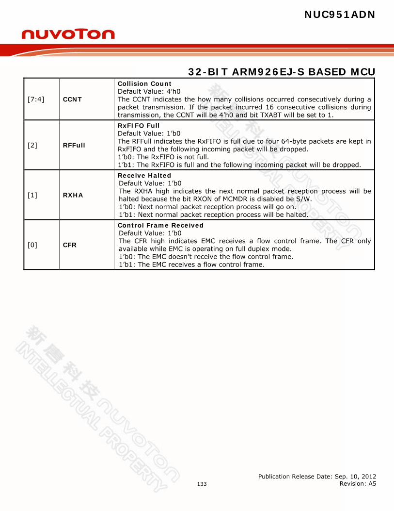
NUC951ADN
32-BIT ARM926EJ-S BASED MCU
Publication Release Date: Sep. 10, 2012 Revision: A5
133
[7:4] CCNT
Collision Count Default Value: 4’h0 The CCNT indicates the how many collisions occurred consecutively during a packet transmission. If the packet incurred 16 consecutive collisions during transmission, the CCNT will be 4’h0 and bit TXABT will be set to 1.
[2] RFFull
RxFIFO Full Default Value: 1’b0 The RFFull indicates the RxFIFO is full due to four 64-byte packets are kept in RxFIFO and the following incoming packet will be dropped. 1’b0: The RxFIFO is not full. 1’b1: The RxFIFO is full and the following incoming packet will be dropped.
[1] RXHA
Receive Halted Default Value: 1’b0 The RXHA high indicates the next normal packet reception process will be halted because the bit RXON of MCMDR is disabled be S/W. 1’b0: Next normal packet reception process will go on. 1’b1: Next normal packet reception process will be halted.
[0] CFR
Control Frame Received Default Value: 1’b0 The CFR high indicates EMC receives a flow control frame. The CFR only available while EMC is operating on full duplex mode. 1’b0: The EMC doesn’t receive the flow control frame. 1’b1: The EMC receives a flow control frame.
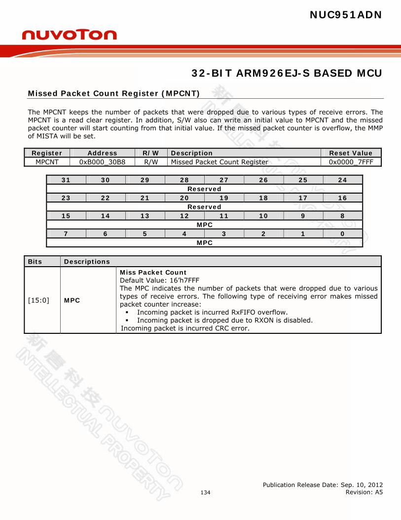
NUC951ADN
32-BIT ARM926EJ-S BASED MCU
Publication Release Date: Sep. 10, 2012 Revision: A5
134
Missed Packet Count Register (MPCNT)
The MPCNT keeps the number of packets that were dropped due to various types of receive errors. The MPCNT is a read clear register. In addition, S/W also can write an initial value to MPCNT and the missed packet counter will start counting from that initial value. If the missed packet counter is overflow, the MMP of MISTA will be set. Register Address R/W Description Reset Value MPCNT 0xB000_30B8 R/W Missed Packet Count Register 0x0000_7FFF
31 30 29 28 27 26 25 24
Reserved 23 22 21 20 19 18 17 16
Reserved 15 14 13 12 11 10 9 8
MPC 7 6 5 4 3 2 1 0
MPC Bits Descriptions
[15:0] MPC
Miss Packet Count Default Value: 16’h7FFF The MPC indicates the number of packets that were dropped due to various types of receive errors. The following type of receiving error makes missed packet counter increase: Incoming packet is incurred RxFIFO overflow. Incoming packet is dropped due to RXON is disabled.
Incoming packet is incurred CRC error.

NUC951ADN
32-BIT ARM926EJ-S BASED MCU
Publication Release Date: Sep. 10, 2012 Revision: A5
135
MAC Receive Pause Count Register (MRPC)
The EMC of NUC910ABN supports the PAUSE control frame reception and recognition. If EMC received a PAUSE control frame, the operand field of the PAUSE control frame will be extracted and stored in the MRPC register. The MRPC register will keep the same while Tx of EMC is pausing due to the PAUSE control frame is received. The MRPC is read only and write to this register has no effect. Register Address R/W Description Reset Value
MRPC 0xB000_30BC R MAC Receive Pause Count Register 0x0000_0000
31 30 29 28 27 26 25 24 Reserved
23 22 21 20 19 18 17 16 Reserved
15 14 13 12 11 10 9 8 MRPC
7 6 5 4 3 2 1 0 MRPC
Bits Descriptions
[15:0] MRPC
MAC Receive Pause Count Default Value: 16’h0 The MRPC keeps the operand field of the PAUSE control frame. It indicates how many slot time (512 bit time) the Tx of EMC will be paused.

NUC951ADN
32-BIT ARM926EJ-S BASED MCU
Publication Release Date: Sep. 10, 2012 Revision: A5
136
MAC Receive Pause Current Count Register (MRPCC)
The EMC of NUC910ABN supports the PAUSE control frame reception and recognition. If EMC received a PAUSE control frame, the operand field of the PAUSE control frame will be extracted and stored into a down count timer. The MRPCC shows the current value of that down count timer for S/W to know how long the Tx of EMC will be paused. The MRPCC is read only and write to this register has no effect. Register Address R/W Description Reset Value MRPCC 0xB000_30C0 R MAC Receive Pause Current Count Register 0x0000_0000
31 30 29 28 27 26 25 24
Reserved 23 22 21 20 19 18 17 16
Reserved 15 14 13 12 11 10 9 8
MRPCC 7 6 5 4 3 2 1 0
MRPCC Bits Descriptions
[15:0] MRPCC
MAC Receive Pause Current Count Default Value: 16’h0 The MRPCC shows the current value of that down count timer. If a new PAUSE control frame is received before the timer count down to zero, the new operand of the PAUSE control frame will be stored into the down count timer and the timer starts count down from the new value.
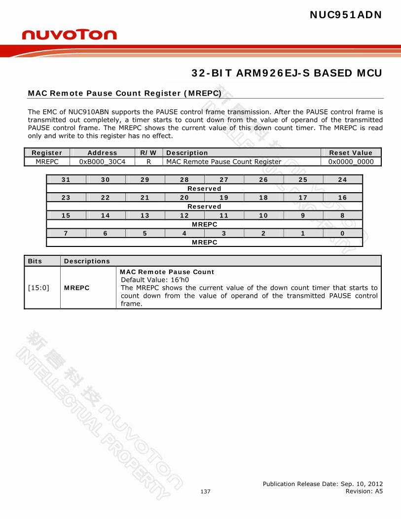
NUC951ADN
32-BIT ARM926EJ-S BASED MCU
Publication Release Date: Sep. 10, 2012 Revision: A5
137
MAC Remote Pause Count Register (MREPC)
The EMC of NUC910ABN supports the PAUSE control frame transmission. After the PAUSE control frame is transmitted out completely, a timer starts to count down from the value of operand of the transmitted PAUSE control frame. The MREPC shows the current value of this down count timer. The MREPC is read only and write to this register has no effect. Register Address R/W Description Reset Value MREPC 0xB000_30C4 R MAC Remote Pause Count Register 0x0000_0000
31 30 29 28 27 26 25 24
Reserved 23 22 21 20 19 18 17 16
Reserved 15 14 13 12 11 10 9 8
MREPC 7 6 5 4 3 2 1 0
MREPC Bits Descriptions
[15:0] MREPC
MAC Remote Pause Count Default Value: 16’h0 The MREPC shows the current value of the down count timer that starts to count down from the value of operand of the transmitted PAUSE control frame.
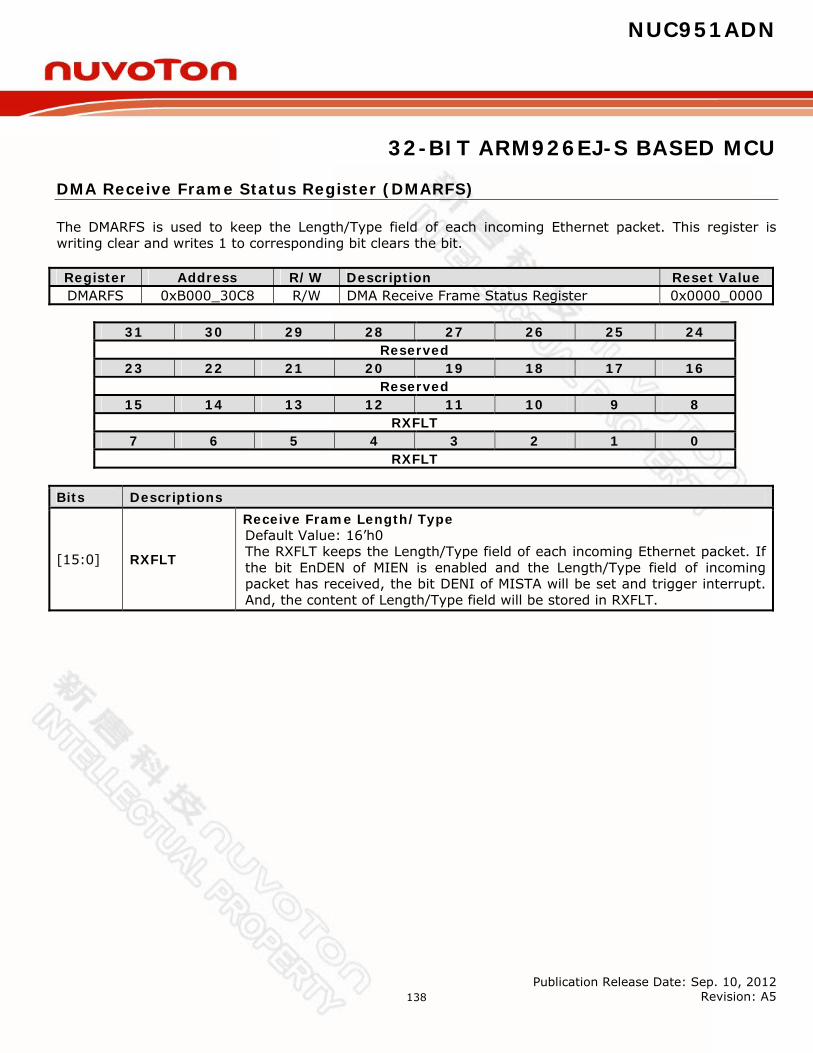
NUC951ADN
32-BIT ARM926EJ-S BASED MCU
Publication Release Date: Sep. 10, 2012 Revision: A5
138
DMA Receive Frame Status Register (DMARFS)
The DMARFS is used to keep the Length/Type field of each incoming Ethernet packet. This register is writing clear and writes 1 to corresponding bit clears the bit. Register Address R/W Description Reset Value DMARFS 0xB000_30C8 R/W DMA Receive Frame Status Register 0x0000_0000
31 30 29 28 27 26 25 24
Reserved 23 22 21 20 19 18 17 16
Reserved 15 14 13 12 11 10 9 8
RXFLT 7 6 5 4 3 2 1 0
RXFLT Bits Descriptions
[15:0] RXFLT
Receive Frame Length/Type Default Value: 16’h0 The RXFLT keeps the Length/Type field of each incoming Ethernet packet. If the bit EnDEN of MIEN is enabled and the Length/Type field of incoming packet has received, the bit DENI of MISTA will be set and trigger interrupt. And, the content of Length/Type field will be stored in RXFLT.
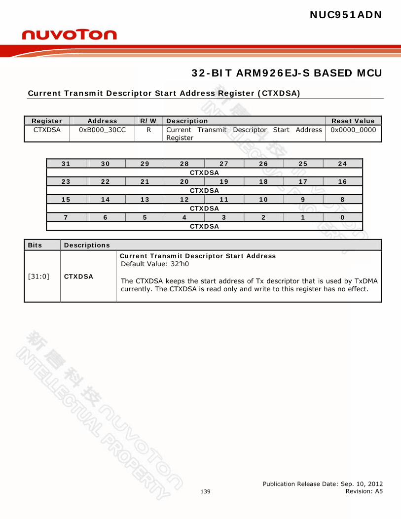
NUC951ADN
32-BIT ARM926EJ-S BASED MCU
Publication Release Date: Sep. 10, 2012 Revision: A5
139
Current Transmit Descriptor Start Address Register (CTXDSA)
Register Address R/W Description Reset Value CTXDSA 0xB000_30CC R Current Transmit Descriptor Start Address
Register 0x0000_0000
31 30 29 28 27 26 25 24 CTXDSA
23 22 21 20 19 18 17 16 CTXDSA
15 14 13 12 11 10 9 8 CTXDSA
7 6 5 4 3 2 1 0 CTXDSA
Bits Descriptions
[31:0] CTXDSA
Current Transmit Descriptor Start Address Default Value: 32’h0
The CTXDSA keeps the start address of Tx descriptor that is used by TxDMA currently. The CTXDSA is read only and write to this register has no effect.

NUC951ADN
32-BIT ARM926EJ-S BASED MCU
Publication Release Date: Sep. 10, 2012 Revision: A5
140
Current Transmit Buffer Start Address Register (CTXBSA)
Register Address R/W Description Reset Value CTXBSA 0xB000_30D0 R Current Transmit Buffer Start Address Register 0x0000_0000
31 30 29 28 27 26 25 24
CTXBSA 23 22 21 20 19 18 17 16
CTXBSA 15 14 13 12 11 10 9 8
CTXBSA 7 6 5 4 3 2 1 0
CTXBSA Bits Descriptions
[31:0] CTXBSA
Current Transmit Buffer Start Address Default Value: 32’h0
The CTXDSA keeps the start address of Tx frame buffer that is used by TxDMA currently. The CTXBSA is read only and write to this register has no effect.
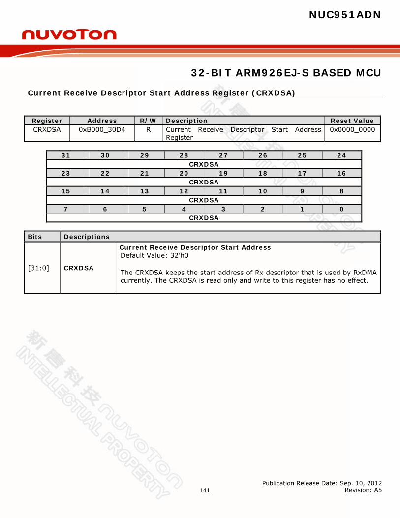
NUC951ADN
32-BIT ARM926EJ-S BASED MCU
Publication Release Date: Sep. 10, 2012 Revision: A5
141
Current Receive Descriptor Start Address Register (CRXDSA)
Register Address R/W Description Reset Value CRXDSA 0xB000_30D4 R Current Receive Descriptor Start Address
Register 0x0000_0000
31 30 29 28 27 26 25 24
CRXDSA 23 22 21 20 19 18 17 16
CRXDSA 15 14 13 12 11 10 9 8
CRXDSA 7 6 5 4 3 2 1 0
CRXDSA Bits Descriptions
[31:0] CRXDSA
Current Receive Descriptor Start Address Default Value: 32’h0
The CRXDSA keeps the start address of Rx descriptor that is used by RxDMA currently. The CRXDSA is read only and write to this register has no effect.
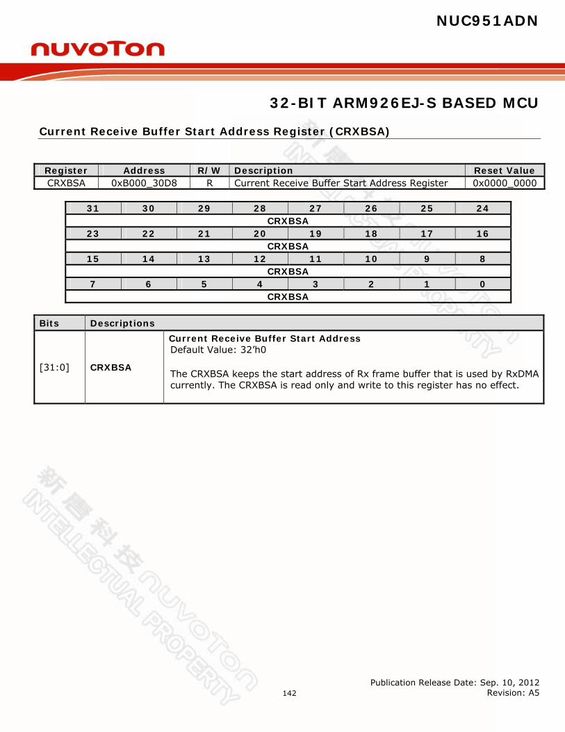
NUC951ADN
32-BIT ARM926EJ-S BASED MCU
Publication Release Date: Sep. 10, 2012 Revision: A5
142
Current Receive Buffer Start Address Register (CRXBSA)
Register Address R/W Description Reset Value CRXBSA 0xB000_30D8 R Current Receive Buffer Start Address Register 0x0000_0000
31 30 29 28 27 26 25 24
CRXBSA 23 22 21 20 19 18 17 16
CRXBSA 15 14 13 12 11 10 9 8
CRXBSA 7 6 5 4 3 2 1 0
CRXBSA Bits Descriptions
[31:0] CRXBSA
Current Receive Buffer Start Address Default Value: 32’h0
The CRXBSA keeps the start address of Rx frame buffer that is used by RxDMA currently. The CRXBSA is read only and write to this register has no effect.
NUC951ADN
32-BIT ARM926EJ-S BASED MCU
Publication Release Date: Sep. 10, 2012 Revision: A5
143
7.5.4 Operation Notes MII Management Interface The operation mode between EMC and external PHY must be identically. Consequently, S/W has to access control register of external PHY through MII management interface to get operation information of PHY. To issue MII management command to access external PHY, the MIID and MIIDA registers can be used. And, while using MII management interface, the EnMDC of MCMDR register must be set to high.
EMC Initial If S/W wants to enable EMC for packet transmission and reception, the TXON and RXON of MCMDR register must be enabled. But, before enabling TXON and RXON, the following issues must be noted. For packet transmission, the Tx descriptor link list and Tx frame buffer must be prepared and TXDLSA must be configured. For incoming packet destination MAC address recognition, the CAMCMR, CAMEN, CAMxM and CAMxL registers must be configured. For incoming packet’s buffering, the Rx descriptor link list and Rx frame buffer must be prepared and RXDLSA register must be configured. Besides, the interrupt status that S/W wants to know must be enabled through MIEN register. Finally, the EMC operation mode control bits of MCMDR must be configured and TXON and RXON must be enabled.
MAC Interrupt Status Register (MISTA) The MISTA register keeps the status of EMC operation. It is recommended that S/W must enable four interrupt statuses at least. They are TxBErr, RxBErr, TDU and RDU. While EMC accesses memory, it reports the memory error through TxBErr or TxBErr status. If any of them actives, the reset EMC is recommended. For packet transmission, a valid Tx descriptor is required, and for packet reception, a valid Rx one is. If EMC cannot find a valid Tx or Rx descriptor, it sets TDU or RDU to high respectively. After S/W releases a valid Tx or Rx descriptor to EMC, writing TSDR or RSDR register to enable packet transmission and reception again is needed.
Pause Control Frame Transmission The EMC support the PAUSE control frame transmission for flow control while EMC is operating on full-duplex mode. The register CAM13M, CAM13L, CAM14M, CAM14L, CAM15M and CAM15L are designed for this purpose. For PAUSE control frame transmission, first, S/W must configure destination MAC address of control frame into the register pair CAM13M, CAM13L, source MAC address into the register pair CAM14M, CAM14L, and configure length/type, op-code and operand of control frame into the register pair CAM15M, CAM15L. The bit CAM13EN, CAM14EN and CAM15EN of CAMEN register are also needed be enabled. Then, set bit SDPZ of MCMDR register to high to enable PAUSE control frame transmission. After the PAUSE control frame transmission completed, the SDPZ will be cleared automatically.
Internal Loop-back If the LBK of MCMDR register is set, the EMC operates on internal loop-back mode. While EMC operates on internal loop-back mode, it also means EMC operates on full-duplex mode, and the value of FDUP of MCMDR register is ignored.
NUC951ADN
32-BIT ARM926EJ-S BASED MCU
Publication Release Date: Sep. 10, 2012 Revision: A5
144
7.6 GDMA Controller
7.6.1 Overview & Features The chip has a two-channel general DMA controller with or without descriptor fetch operation, called the GDMA. The two-channel GDMA performs the following data transfers without the CPU intervention:
Memory-to-memory (memory to/from memory) Memory –to – IO IO- to -memory
The on-chip GDMA can be started by the software or external DMA request nXDREQ0. Software can also be used to restart the GDMA operation after it has been stopped. The CPU can recognize the completion of a GDMA operation by software polling or when it receives an internal GDMA interrupt. The GDMA controller can increment source or destination address, decrement them as well, and conduct 8-bit (byte), 16-bit (half-word), or 32-bit (word) data transfers.
7.6.2 GDMA Non-Descriptor Functional Description
The GDMA directly transfers data between source and destination. The GDMA starts to transfer data after it receives service requests from nXDREQ0 signal or software. When the entire data have been transferred completely, the GDMA becomes idle. Nevertheless, if another transfer is needed, then the GDMA must be programmed again. There are three transfer modes:
Single Mode Single mode requires a GDMA request for each data transfer. A GDMA request (nXDREQ0 or software) causes one byte, one half-word, or one word to transfer if the 4-data burst mode is disabled, or four times of transfer width is the 4-data burst mode is enabled.
Block Mode
The assertion of a single GDMA request causes all of the data to be transferred in a single operation. The GDMA transfer is completed when the current transfer count register reaches zero.
Demand Mode
The GDMA continues transferring data until the GDMA request input nXDREQ0 becomes inactive.
NUC951ADN
32-BIT ARM926EJ-S BASED MCU
Publication Release Date: Sep. 10, 2012 Revision: A5
145
7.6.3 GDMA Descriptor Functional Description The descriptor-fetch function works when run-bit (bit-3) is set and non-dsptrmode-bit (bit-2) is cleared in Descriptor Register (GDMA_DADRx) and the GDMA_CTLx bit setting as following table. The Non-descriptor-fetch function works when software triggers the [softreq] bit (bit-16) and the [gdmaen] bit (bit-0) in GDMA_CTLx Register. If the [softreq] set to zero and the [GDMAMS] (bit2-3) set as 01 or 10 will start the I/O to memory function. Software can also be used to restart the GDMA operation after it has been stopped. The CPU can recognize the completion of a GDMA operation by software polling or when it receives an internal GDMA interrupt. The GDMA controller can increase source or destination address, decrease them as well, and conduct 8-bit (byte), 16-bit (half-word), or 32-bit (word) data transfers. Operation Mode relevant to enable bit Mode Enable bit Non-Descriptor Mode with SW Enable GDMA_CTLx : gdmaen[0] softreq[16] gdmams[3:2] Non-Descriptor Mode with I/O Enable GDMA_CTLx : gdmaen[0] gdmams[3:2] Descriptor Mode with SW Enable GDMA_DADRx : run[3] non-dsptrmode[2];
GDMA_CTLx in Descriptor List : gdmaen[0] gdmams[3:2] Descriptor Mode with I/O Enable GDMA_DADRx : run[3] non-dsptrmode[2];
GDMA_CTLx in Descriptor List : gdmaen[0] gdmams[3:2]

NUC951ADN
32-BIT ARM926EJ-S BASED MCU
Publication Release Date: Sep. 10, 2012 Revision: A5
146
7.6.3.1 Descriptor Fetch Function The Illustration of Descriptor list fetches:
Memory
Next Descriptor Address 0
Source Address 0
Destination Address 0
Command Information 0
Next Descriptor Address 1
Source Address 1
Destination Address 1
Command Information 1
Next Descriptor Address 2
Source Address 2
.
.
.
Next Descriptor Address
Source Address x
Destination Address x
Command Information x
GDMA_DADRx[31:4] + 0x00
Ordering
Programming by software
GDMA_DADRx[31:4] + 0x10
GDMA_DADRx[31:4] + 0x10
GDMA_DADRx
GDMA Fetch Descriptor
Single Channel Descriptor
Internal Descriptor Register
GDMA_SRCBx
GDMA_DSTBx
GDMA_TCNTx
GDMA_CTLx
GDMA
A Descriptor list finished
Bit[31:18]
Bit[17:0]
Bit[31:0]
Bit[31:0]
Bit[31:0]
GDMA_DADRx[31:4] + 0x04
GDMA_DADRx[31:4] + 0x08
GDMA_DADRx[31:4] + 0x0C
GDMA_DADRx[31:4] + 0x00
GDMA_DADRx[31:4] + 0x04
GDMA_DADRx[31:4] + 0x08
GDMA_DADRx[31:4] + 0x0C
GDMA_DADRx[31:4] + 0x00
GDMA_DADRx[31:4] + 0x04
GDMA_DADRx[31:4] + 0x00
GDMA_DADRx[31:4] + 0x04
GDMA_DADRx[31:4] + 0x08
GDMA_DADRx[31:4] + 0x0C

NUC951ADN
32-BIT ARM926EJ-S BASED MCU
Publication Release Date: Sep. 10, 2012 Revision: A5
147
Descriptor-based function (GDMA_DADRx [NON_DSPTRMODE] = 0) operate in the following condition: Memory to Memory 1. Software can write a value 0x04 to current GDMA_DADRx register to reset the register and disable
Descriptor based function first. 2. Then software can program the bits of [Descriptor Address], [RUN], [NON_DSPTRMODE] and [ORDEN]
to the GDMA_DADRx register to enable Descriptor based function. (The Descriptor can only work when the [RUN] [3] is set and [NON_DSPTRMODE] [2] bit is cleared properly.)
3. After sets current GDMA_DADRx register, the GDMA will fetch four-word information from memory immediately which contains the next Descriptor address, Source Address, Destination Address and Command information. (Command information consists of control and counter registers)
NOTE: GDMA will read the descriptor list from memory such the diagram above and write back to GDMA
internal register (next GDMA_DADRx), GDMA_SRCBx, GDMA_DSTBx, GDMA_CTLx and GDMA_TCNTx registers. The most important one of write back is command information, which will separate some bits of command information into control and counter registers respectively. The first fourteen bits of the MSB of the Command information in Descriptor list will be written back to GDMA_TCNTx register, and the others bits of the Command information will be written back to GDMA_CTLx register. The control register part of the Command information will update the GDMA_CTLx register during every descriptor fetch. The allocation of command information is described at GDMA Register Descriptions.
The Allocation of Command Information in Descriptor List:
4. GDMA will depend on the information to request a bus ownership and start the data transfer when
GDMA has gotten a bus grant from the arbiter, otherwise, it will wait until get bus grant. The data transfer direction is dependent on the Control register.
5. The GDMA transfers data and releases bus at every burst transfer. The GDMA will stop transfer for current descriptor when the counter is decreased to zero. The current GDMA_DADRx will be updated by next GDMA_DADRx at end of each descriptor transfer.
6. The GDMA is running consecutively unless the next GDMA_DADRx[RUN] bit is zero or interrupt status bit of GDMA_INTCS register is cleared. The CPU can recognize the completion of a GDMA descriptor fetch operation by polling the current GDMA_DADRx[NON_DSPTRMODE] bit or set the GDMA_CTLx[D_INTS] to receive a interrupt from GDMA.(Note: The recommendation is the [NON_DSPTRMODE] bit in list is set at the same time)
7. When an error occurs in the descriptor operation, GDMA will clear [RUN] bit and stop channel operation immediately. Software can reset the channel, and sets the current GDMA_DADRx [RUN] register to start again.
31 30 29 28 27 26 25 24 GDMA_TCNTx[13:6] Command Info[31:24]
23 22 21 20 19 18 17 16 GDMA_TCNTx[5:0] Command Info[23:18] BLOCK SOFTREQ
15 14 13 12 11 10 9 8 TWS RESERVED D_INTS D_INTS RESERVED
7 6 5 4 3 2 1 0 SAFIX DAFIX SADIR DADIR GDMAMS BME GDMAEN

NUC951ADN
32-BIT ARM926EJ-S BASED MCU
Publication Release Date: Sep. 10, 2012 Revision: A5
148
Memory to I/O and I/O to Memory 1. Software must set the [REQ_ATV], [ACK_ATV] and [GDMAMS] bits in GDMA_CTLx register
corresponding to I/O pin with pull high or pull low properly first, and then set the current GDMA_DADRx to start the I/O to Memory with descriptor fetch transfer.
2. The descriptor lists stop transfer until the RUN bit was zero in descriptor list when external I/O request triggered once. The RUN bit can be set when external I/O request triggered again under the NON_DSPTRMODE bit was zero in descriptor list. The trigger period of the external I/O has a timing limitation whatever the GDMA was in single or burst mode, and the periodic trigger of the external I/O must be less than 38 MCLK.
3. Each GDMA lists can operate after clearing interrupt status. The descriptor lists stop transfer until the RUN bit was zero or interrupt status was set.
4. The next Descriptor address, Source Address, Destination Address and Command information must be set properly in every Descriptor list. Especially, every bit of the Command information will update the GDMA_CTLx and GDMA_TCNTx registers at every initiation of descriptor list.
NOTE: The [BLOCK] bit of GDMA_CTLx register is disabled when the descriptor mode of the I/O to memory is enabled. NOTE: GDMA can change mode with following description: Descriptor-fetch of each channel can be stopped until the current transfer list done. Software can change Descriptor mode to Non-Descritpor mode by writing 0x04 to GDMA_DADRx register during the current descriptor transfer operating. Non-Descriptor fetch can be stopped until current transfer count finished when software programs the GDMA_CTLx register with gdmaen bit cleared or softreq cleared. NOTE: Once software programs the current GDMA_DADRx register, GDMA will fetch the descriptor list from memory and fill the data to next GDMA_DADRx, current GDMA_SRCBx, current GDMA_DSTBx, current GDMA_CTLx and current GDMA_TCNTx registers automatically. The fourth word in descriptor list includes the information for GDMA_CTLx and GDMA_TCNTx registers. NOTE: The descriptor fetch function only occurs when current GDMA_DADRx [RUN] bit is set and GDMA_DADRx [NON_DSPTRMODE] is cleared. The current GDMA_DADRx will be updated by next GDMA_DADRx at every descriptor stops.
7.6.3.2 Ordering function in Descriptor fetch mode This function determines the source of next descriptor address. If [ORDEN] is set, the GDMA controller fetches the next descriptor from current GDMA_DADRx [Descriptor Address] + 16 bytes. If this bit is cleared, GDMA fetches the next descriptor from the current GDMA_DADRx [Descriptor Address]. GDMA_DADRx [ORDEN] is only relevant to descriptor-fetch function (GDMA_DADRx [NON_DSPTRMODE] = 0).
7.6.3.3 Channel Reset The Channel reset is turned on when the bit-0 of GDMA_DADRx is set. This function will clear all status
NUC951ADN
32-BIT ARM926EJ-S BASED MCU
Publication Release Date: Sep. 10, 2012 Revision: A5
149
and stop the descriptor based function relative to individual channel. The GDMA_DADRx register value is 0x05h when reset bit is set.
7.6.3.4 Non-Descriptor Fetch Function The non-descriptor-fetch function will take place when current GDMA_DADRx [NON_DSPTRMODE] is set and the GDMA_DADRx register will have no any intention for the GDMA controller. The default value of GDMA_DADRx is 0x04. Software can clear GDMA_DADRx with value 0x04 as well. In this mode, software should write a valid source address to the GDMA_SRCBx register, a destination address to the GDMA_DSTBx register, and a transfer count to the GDMA_TCNTx register. Next, the GDMA_CTLx of [gdmaen] and [softreq] bits must be set. A non-descriptor fetch is performed when bus granted. After transferring a number of bytes or words correspond with burst mode or not, the channel either waits for the next request or continues with the data transfer until the GDMA_CTCNTx reaches zero. When GDMA_CTCNTx reaches zero, the channel stops operation. When an error occurs during the GDMA operation, the channel stops unless software clears the error condition and sets the GDMA_CTLx of [gdmaen] and [softreq] bits field to start again.

NUC951ADN
32-BIT ARM926EJ-S BASED MCU
Publication Release Date: Sep. 10, 2012 Revision: A5
150
7.6.4 GDMA Register Map
R: read only, W: write only, R/W: both read and write, C: Only value 0 can be written Register Address R/W Description Reset Value
GDMA_BA = 0xB000_4000
Channel 0
GDMA_CTL0 0xB000_4000 R/W Channel 0 Control Register 0x0000_0000 GDMA_SRCB0 0xB000_4004 R/W Channel 0 Source Base Address Register 0x0000_0000 GDMA_DSTB0 0xB000_4008 R/W Channel 0 Destination Base Address Register 0x0000_0000 GDMA_TCNT0 0xB000_400C R/W Channel 0 Transfer Count Register 0x0000_0000 GDMA_CSRC0 0xB000_4010 R Channel 0 Current Source Address Register 0x0000_0000 GDMA_CDST0 0xB000_4014 R Channel 0 Current Destination Address Reg. 0x0000_0000 GDMA_CTCNT0 0xB000_4018 R Channel 0 Current Transfer Count Register 0x0000_0000 GDMA_DADR0 0xB000_401C R/W Channel 0 Descriptor Address Register 0x0000_0004
Channel 1
GDMA_CTL1 0xB000_4020 R/W Channel 1 Control Register 0x0000_0000 GDMA_SRCB1 0xB000_4024 R/W Channel 1 Source Base Address Register 0x0000_0000 GDMA_DSTB1 0xB000_4028 R/W Channel 1 Destination Base Address Register 0x0000_0000 GDMA_TCNT1 0xB000_402C R/W Channel 1 Transfer Count Register 0x0000_0000 GDMA_CSRC1 0xB000_4030 R Channel 1 Current Source Address Register 0x0000_0000 GDMA_CDST1 0xB000_4034 R Channel 1 Current Destination Address Reg. 0x0000_0000 GDMA_CTCNT1 0xB000_4038 R Channel 1 Current Transfer Count Register 0x0000_0000 GDMA_DADR1 0xB000_403C R/W Channel 1 Descriptor Address Register 0x0000_0004
GDMA_INTBUF0 0xB000_4080 R GDMA Internal Buffer Word 0 0x0000_0000
GDMA_INTBUF1 0xB000_4084 R GDMA Internal Buffer Word 1 0x0000_0000
GDMA_INTBUF2 0xB000_4088 R GDMA Internal Buffer Word 2 0x0000_0000
GDMA_INTBUF3 0xB000_408C R GDMA Internal Buffer Word 3 0x0000_0000
GDMA_INTBUF4 0xB000_4090 R GDMA Internal Buffer Word 4 0x0000_0000
GDMA_INTBUF5 0xB000_4094 R GDMA Internal Buffer Word 5 0x0000_0000
GDMA_INTBUF6 0xB000_4098 R GDMA Internal Buffer Word 6 0x0000_0000
GDMA_INTBUF7 0xB000_409C R GDMA Internal Buffer Word 7 0x0000_0000
GDMA_INTCS 0xB000_40A0 R/W Interrupt Control and Status Register (2 Channels) 0x0000_0000
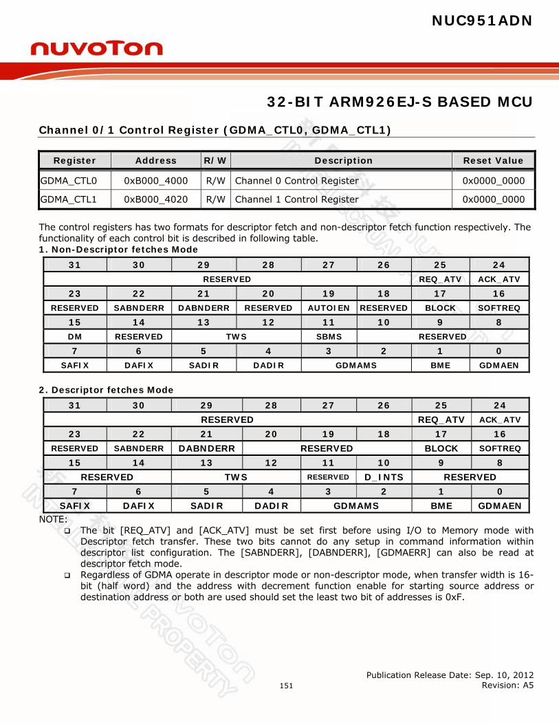
NUC951ADN
32-BIT ARM926EJ-S BASED MCU
Publication Release Date: Sep. 10, 2012 Revision: A5
151
Channel 0/1 Control Register (GDMA_CTL0, GDMA_CTL1)
Register Address R/W Description Reset Value
GDMA_CTL0 0xB000_4000 R/W Channel 0 Control Register 0x0000_0000
GDMA_CTL1 0xB000_4020 R/W Channel 1 Control Register 0x0000_0000
The control registers has two formats for descriptor fetch and non-descriptor fetch function respectively. The functionality of each control bit is described in following table. 1. Non-Descriptor fetches Mode
2. Descriptor fetches Mode
NOTE: The bit [REQ_ATV] and [ACK_ATV] must be set first before using I/O to Memory mode with
Descriptor fetch transfer. These two bits cannot do any setup in command information within descriptor list configuration. The [SABNDERR], [DABNDERR], [GDMAERR] can also be read at descriptor fetch mode.
Regardless of GDMA operate in descriptor mode or non-descriptor mode, when transfer width is 16-bit (half word) and the address with decrement function enable for starting source address or destination address or both are used should set the least two bit of addresses is 0xF.
31 30 29 28 27 26 25 24 RESERVED REQ_ATV ACK_ATV
23 22 21 20 19 18 17 16 RESERVED SABNDERR DABNDERR RESERVED AUTOIEN RESERVED BLOCK SOFTREQ
15 14 13 12 11 10 9 8 DM RESERVED TWS SBMS RESERVED
7 6 5 4 3 2 1 0 SAFIX DAFIX SADIR DADIR GDMAMS BME GDMAEN
31 30 29 28 27 26 25 24 RESERVED REQ_ATV ACK_ATV
23 22 21 20 19 18 17 16 RESERVED SABNDERR DABNDERR RESERVED BLOCK SOFTREQ
15 14 13 12 11 10 9 8 RESERVED TWS RESERVED D_INTS RESERVED
7 6 5 4 3 2 1 0 SAFIX DAFIX SADIR DADIR GDMAMS BME GDMAEN

NUC951ADN
32-BIT ARM926EJ-S BASED MCU
Publication Release Date: Sep. 10, 2012 Revision: A5
152
Control Register of Non-Descriptor fetches Mode: Bits Descriptions
[25] REQ_ATV
REQ_ATV [25]: nXDREQ High/Low active selection If REQ_ATV [25] =0, nXDREQ is LOW active. If REQ_ATV [25] =1, nXDREQ is HIGH active.
[24] ACK_ATV
ACK_ATV [24]: nXDACK High/Low active selection If ACK_ATV [24] =0, nXDACK is LOW active. If ACK_ATV [24] =1, nXDACK is HIGH active.
[22] SABNDERR
Source Address Boundary Alignment Error Flag If TWS [13:12]=10, GDMA_SRCB [1:0] should be 00 If TWS [13:12]=01, GDMA_SRCB [0] should be 0 Except the SADIR function enabled.
The address boundary alignment should be depended on TWS [13:12]. 0 = the GDMA_SRCB is on the boundary alignment. 1 = the GDMA_SRCB not on the boundary alignment The SABNDERR register bits just can be read only.
[21] DABNDERR
Destination Address Boundary Alignment Error Flag If TWS [13:12]=10, GDMA_DSTB [1:0] should be 00 If TWS [13:12]=01, GDMA_DSTB [0] should be 0 Except the SADIR function enabled.
The address boundary alignment should be depended on TWS [13:12]. 0 = the GDMA_DSTB is on the boundary alignment. 1 = the GDMA_DSTB not on the boundary alignment The DABNDERR register bits just can be read only.
[19] AUTOIEN
Auto initialization Enable 0 = Disables auto initialization 1 = Enables auto initialization, the GDMA_CSRC0/1, GDMA_CDST0/1, and
GDMA_CTCNT0/1 registers are updated by the GDMA_SRC0/1, GDMA_DST0/1, and GDMA_TCNT0/1 registers automatically when transfer is complete. GDMA will start another transfer when SOFTREQ set again.
[17] BLOCK Bus Lock 0 = Unlocks the bus during the period of transfer 1 = locks the bus during the period of transfer
[16] SOFTREQ
Software Triggered GDMA Request Software can request the GDMA transfer service by setting this bit to 1. This bit is automatically cleared by hardware when the transfer is completed. This bit is available only while GDMAMS [3:2] register bits are set on software mode (memory to memory and memory to I/O).

NUC951ADN
32-BIT ARM926EJ-S BASED MCU
Publication Release Date: Sep. 10, 2012 Revision: A5
153
[15] DM
Demand Mode 0 = Normal external GDMA mode 1 = When this bit is set to 1, the external GDMA operation is speeded up.
When external GDMA device is operating in the demand mode, the GDMA transfers data as long as the external GDMA request signal nXDREQ0 is active. The amount of data transferred depends on how long the nXDREQ0 is active. When the nXDREQ0 is active and GDMA gets the bus in Demand mode, DMA holds the system bus until the nXDREQ0 signal becomes non-active. Therefore, the period of the active nXDREQ0 signal should be carefully tuned such that the entire operation does not exceed an acceptable interval (for example, in a DRAM refresh operation).
[13:12] TWS
Transfer Width Select 00 = One byte (8 bits) is transferred for every GDMA operation 01 = One half-word (16 bits) is transferred for every GDMA operation 10 = One word (32 bits) is transferred for every GDMA operation 11 = Reserved The GDMA_SCRB and GDMA_DSTB should be alignment under the TWS selection
[11] SBMS
Single/Block Mode Select 0 = Selects single mode. It requires an external GDMA request for every
incurring GDMA operation. 1 = Selects block mode. It requires a single external GDMA request during
the atomic GDMA operation. An atomic GDMA operation is defined as the sequence of GDMA operations until the transfer count register reaches zero.
[7] SAFIX
Source Address Fixed 0 = Source address is changed during the GDMA operation 1 = Do not change the destination address during the GDMA operation.
This feature can be used when data were transferred from a single source to multiple destinations.
[6] DAFIX
Destination Address Fixed 0 = Destination address is changed during the GDMA operation 1 = Do not change the destination address during the GDMA operation.
This feature can be used when data were transferred from multiple sources to a single destination.
[5] DADIR Source Address Direction 0 = Source address is incremented successively 1 = Source address is decremented successively
[4] DADIR Destination Address Direction 0 = Destination address is incremented successively 1 = Destination address is decremented successively
[3:2] GDMAMS
GDMA Mode Select 00 = Software mode (memory-to-memory) 01 = External nXDREQ0 mode for external device (I/O to Memory) 10 = Reserved 11 = Reserved
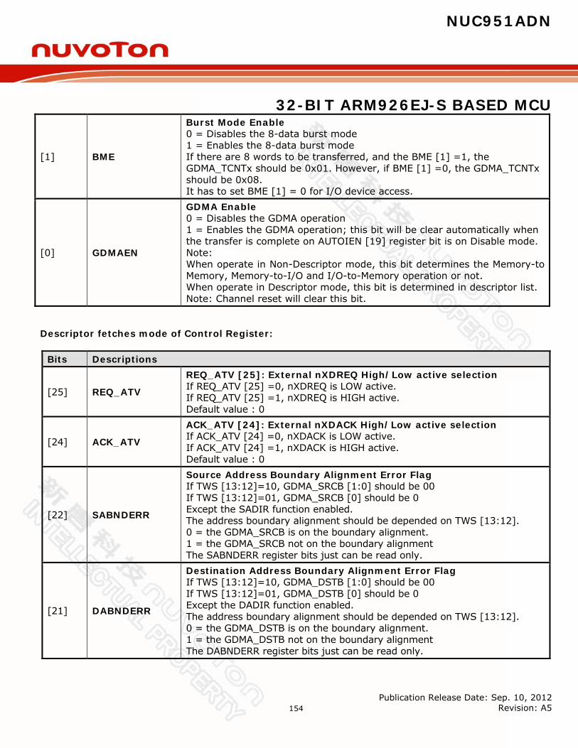
NUC951ADN
32-BIT ARM926EJ-S BASED MCU
Publication Release Date: Sep. 10, 2012 Revision: A5
154
[1] BME
Burst Mode Enable 0 = Disables the 8-data burst mode 1 = Enables the 8-data burst mode If there are 8 words to be transferred, and the BME [1] =1, the GDMA_TCNTx should be 0x01. However, if BME [1] =0, the GDMA_TCNTx should be 0x08. It has to set BME [1] = 0 for I/O device access.
[0] GDMAEN
GDMA Enable 0 = Disables the GDMA operation 1 = Enables the GDMA operation; this bit will be clear automatically when the transfer is complete on AUTOIEN [19] register bit is on Disable mode. Note: When operate in Non-Descriptor mode, this bit determines the Memory-to Memory, Memory-to-I/O and I/O-to-Memory operation or not. When operate in Descriptor mode, this bit is determined in descriptor list. Note: Channel reset will clear this bit.
Descriptor fetches mode of Control Register:
Bits Descriptions
[25] REQ_ATV
REQ_ATV [25]: External nXDREQ High/Low active selection If REQ_ATV [25] =0, nXDREQ is LOW active. If REQ_ATV [25] =1, nXDREQ is HIGH active. Default value : 0
[24] ACK_ATV
ACK_ATV [24]: External nXDACK High/Low active selection If ACK_ATV [24] =0, nXDACK is LOW active. If ACK_ATV [24] =1, nXDACK is HIGH active. Default value : 0
[22] SABNDERR
Source Address Boundary Alignment Error Flag If TWS [13:12]=10, GDMA_SRCB [1:0] should be 00 If TWS [13:12]=01, GDMA_SRCB [0] should be 0 Except the SADIR function enabled. The address boundary alignment should be depended on TWS [13:12]. 0 = the GDMA_SRCB is on the boundary alignment. 1 = the GDMA_SRCB not on the boundary alignment The SABNDERR register bits just can be read only.
[21] DABNDERR
Destination Address Boundary Alignment Error Flag If TWS [13:12]=10, GDMA_DSTB [1:0] should be 00 If TWS [13:12]=01, GDMA_DSTB [0] should be 0 Except the DADIR function enabled. The address boundary alignment should be depended on TWS [13:12]. 0 = the GDMA_DSTB is on the boundary alignment. 1 = the GDMA_DSTB not on the boundary alignment The DABNDERR register bits just can be read only.
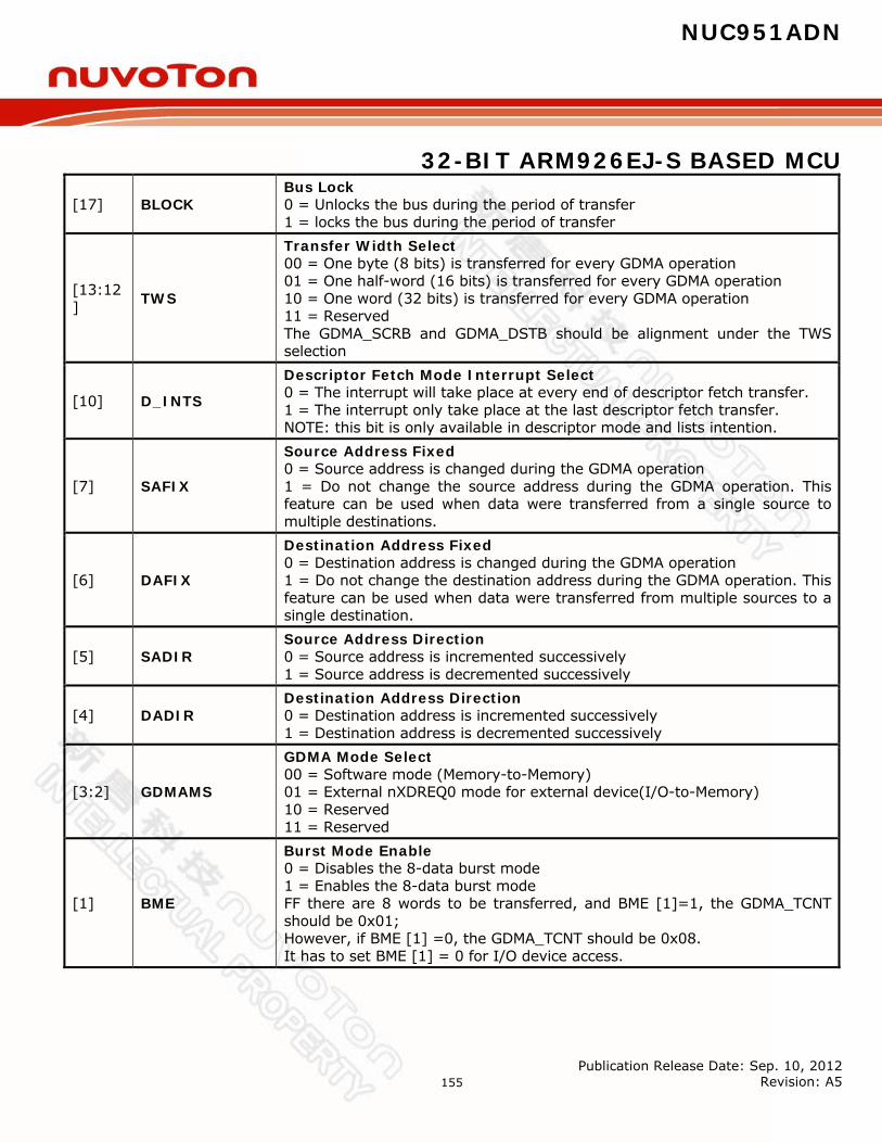
NUC951ADN
32-BIT ARM926EJ-S BASED MCU
Publication Release Date: Sep. 10, 2012 Revision: A5
155
[17] BLOCK Bus Lock 0 = Unlocks the bus during the period of transfer 1 = locks the bus during the period of transfer
[13:12] TWS
Transfer Width Select 00 = One byte (8 bits) is transferred for every GDMA operation 01 = One half-word (16 bits) is transferred for every GDMA operation 10 = One word (32 bits) is transferred for every GDMA operation 11 = Reserved The GDMA_SCRB and GDMA_DSTB should be alignment under the TWS selection
[10] D_INTS
Descriptor Fetch Mode Interrupt Select 0 = The interrupt will take place at every end of descriptor fetch transfer. 1 = The interrupt only take place at the last descriptor fetch transfer. NOTE: this bit is only available in descriptor mode and lists intention.
[7] SAFIX
Source Address Fixed 0 = Source address is changed during the GDMA operation 1 = Do not change the source address during the GDMA operation. This feature can be used when data were transferred from a single source to multiple destinations.
[6] DAFIX
Destination Address Fixed 0 = Destination address is changed during the GDMA operation 1 = Do not change the destination address during the GDMA operation. This feature can be used when data were transferred from multiple sources to a single destination.
[5] SADIR Source Address Direction 0 = Source address is incremented successively 1 = Source address is decremented successively
[4] DADIR Destination Address Direction 0 = Destination address is incremented successively 1 = Destination address is decremented successively
[3:2] GDMAMS
GDMA Mode Select 00 = Software mode (Memory-to-Memory) 01 = External nXDREQ0 mode for external device(I/O-to-Memory) 10 = Reserved 11 = Reserved
[1] BME
Burst Mode Enable 0 = Disables the 8-data burst mode 1 = Enables the 8-data burst mode FF there are 8 words to be transferred, and BME [1]=1, the GDMA_TCNT should be 0x01; However, if BME [1] =0, the GDMA_TCNT should be 0x08. It has to set BME [1] = 0 for I/O device access.

NUC951ADN
32-BIT ARM926EJ-S BASED MCU
Publication Release Date: Sep. 10, 2012 Revision: A5
156
[0] GDMAEN
GDMA Enable 0 = Disables the GDMA operation 1 = Enables the GDMA operation; this bit will be clear automatically when the transfer is complete on AUTOIEN [19] register bit is on Disable mode. When operate in Non-Descriptor mode, this bit determines the Memory-to-Memory, Memory-to-I/O and I/O-to-Memory operation or not. When operate in Descriptor mode, this bit determines the I/O-to-Memory operation or not. Channel reset will clear this bit.

NUC951ADN
32-BIT ARM926EJ-S BASED MCU
Publication Release Date: Sep. 10, 2012 Revision: A5
157
Channel 0/1 Source Base Address Register (GDMA_SRCB0, GDMA_SRCB1)
Register Address R/W Description Reset Value
GDMA_SRCB0 0xB000_4004 R/W Channel 0 Source Base Address Register 0x0000_0000 GDMA_SRCB1 0xB000_4024 R/W Channel 1 Source Base Address Register 0x0000_0000
31 30 29 28 27 26 25 24
SRC_BASE_ADDR [31:24] 23 22 21 20 19 18 17 16
SRC_BASE_ADDR [23:16]
15 14 13 12 11 10 9 8 SRC_BASE_ADDR [15:8]
7 6 5 4 3 2 1 0 SRC_BASE_ADDR [7:0]
Bits Descriptions
[31:0] SRC_BASE_ADDR 32-bit Source Base Address The GDMA channel starts reading its data from the source address as defined in this source base address register.
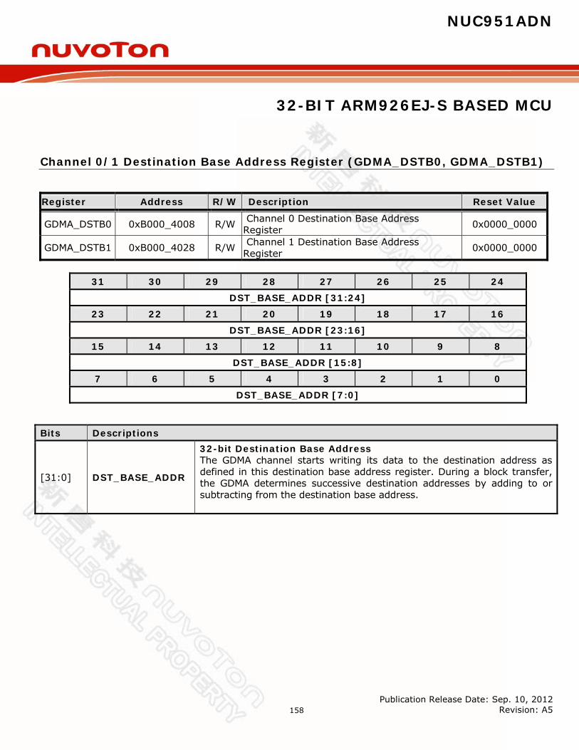
NUC951ADN
32-BIT ARM926EJ-S BASED MCU
Publication Release Date: Sep. 10, 2012 Revision: A5
158
Channel 0/1 Destination Base Address Register (GDMA_DSTB0, GDMA_DSTB1)
Register Address R/W Description Reset Value
GDMA_DSTB0 0xB000_4008 R/W Channel 0 Destination Base Address Register 0x0000_0000
GDMA_DSTB1 0xB000_4028 R/W Channel 1 Destination Base Address Register 0x0000_0000
31 30 29 28 27 26 25 24
DST_BASE_ADDR [31:24] 23 22 21 20 19 18 17 16
DST_BASE_ADDR [23:16]
15 14 13 12 11 10 9 8 DST_BASE_ADDR [15:8]
7 6 5 4 3 2 1 0 DST_BASE_ADDR [7:0]
Bits Descriptions
[31:0] DST_BASE_ADDR
32-bit Destination Base Address The GDMA channel starts writing its data to the destination address as defined in this destination base address register. During a block transfer, the GDMA determines successive destination addresses by adding to or subtracting from the destination base address.
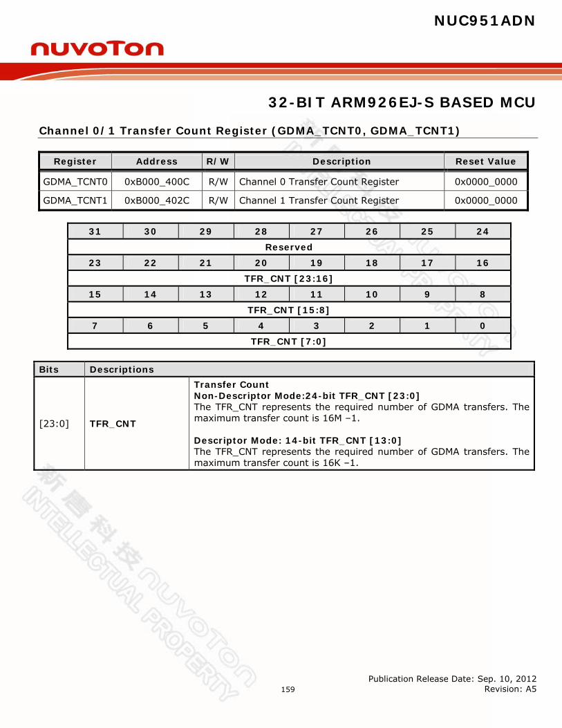
NUC951ADN
32-BIT ARM926EJ-S BASED MCU
Publication Release Date: Sep. 10, 2012 Revision: A5
159
Channel 0/1 Transfer Count Register (GDMA_TCNT0, GDMA_TCNT1)
Register Address R/W Description Reset Value
GDMA_TCNT0 0xB000_400C R/W Channel 0 Transfer Count Register 0x0000_0000
GDMA_TCNT1 0xB000_402C R/W Channel 1 Transfer Count Register 0x0000_0000
31 30 29 28 27 26 25 24
Reserved 23 22 21 20 19 18 17 16
TFR_CNT [23:16]
15 14 13 12 11 10 9 8 TFR_CNT [15:8]
7 6 5 4 3 2 1 0 TFR_CNT [7:0]
Bits Descriptions
[23:0] TFR_CNT
Transfer Count Non-Descriptor Mode:24-bit TFR_CNT [23:0] The TFR_CNT represents the required number of GDMA transfers. The maximum transfer count is 16M –1. Descriptor Mode: 14-bit TFR_CNT [13:0] The TFR_CNT represents the required number of GDMA transfers. The maximum transfer count is 16K –1.
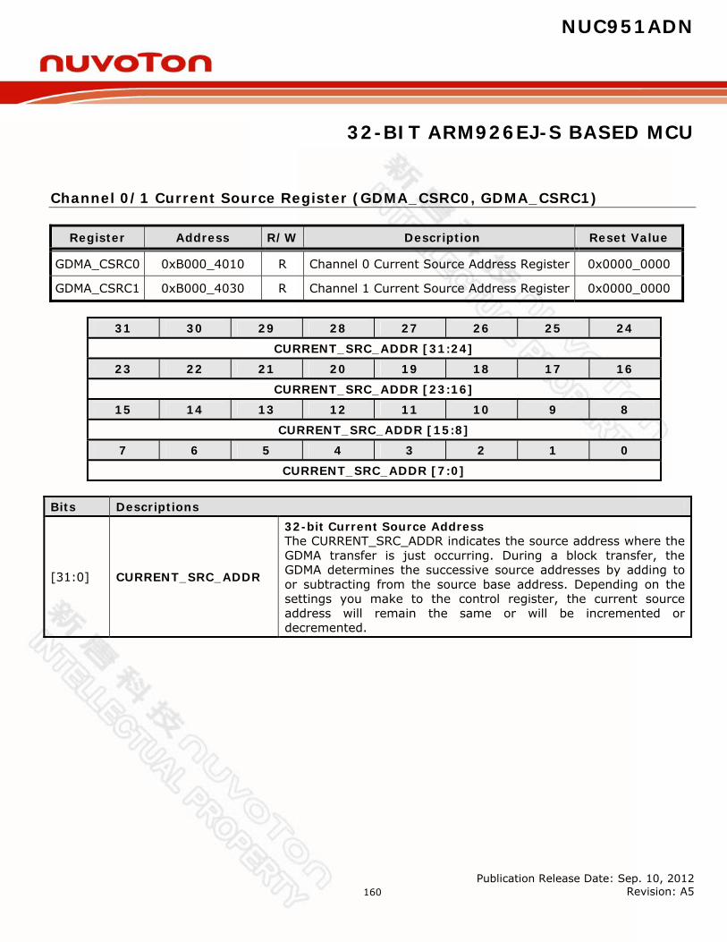
NUC951ADN
32-BIT ARM926EJ-S BASED MCU
Publication Release Date: Sep. 10, 2012 Revision: A5
160
Channel 0/1 Current Source Register (GDMA_CSRC0, GDMA_CSRC1)
Register Address R/W Description Reset Value
GDMA_CSRC0 0xB000_4010 R Channel 0 Current Source Address Register 0x0000_0000
GDMA_CSRC1 0xB000_4030 R Channel 1 Current Source Address Register 0x0000_0000
31 30 29 28 27 26 25 24
CURRENT_SRC_ADDR [31:24] 23 22 21 20 19 18 17 16
CURRENT_SRC_ADDR [23:16]
15 14 13 12 11 10 9 8 CURRENT_SRC_ADDR [15:8]
7 6 5 4 3 2 1 0 CURRENT_SRC_ADDR [7:0]
Bits Descriptions
[31:0] CURRENT_SRC_ADDR
32-bit Current Source Address The CURRENT_SRC_ADDR indicates the source address where the GDMA transfer is just occurring. During a block transfer, the GDMA determines the successive source addresses by adding to or subtracting from the source base address. Depending on the settings you make to the control register, the current source address will remain the same or will be incremented or decremented.
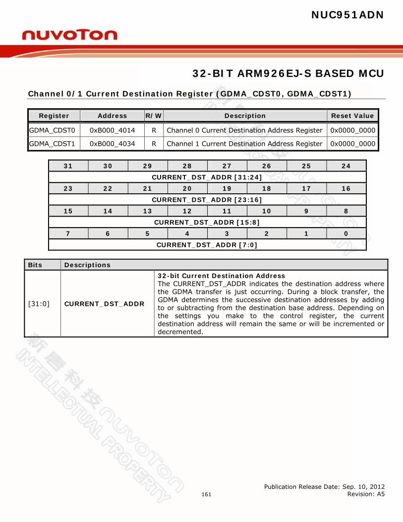
NUC951ADN
32-BIT ARM926EJ-S BASED MCU
Publication Release Date: Sep. 10, 2012 Revision: A5
161
Channel 0/1 Current Destination Register (GDMA_CDST0, GDMA_CDST1)
Register Address R/W Description Reset Value
GDMA_CDST0 0xB000_4014 R Channel 0 Current Destination Address Register 0x0000_0000
GDMA_CDST1 0xB000_4034 R Channel 1 Current Destination Address Register 0x0000_0000
31 30 29 28 27 26 25 24
CURRENT_DST_ADDR [31:24] 23 22 21 20 19 18 17 16
CURRENT_DST_ADDR [23:16]
15 14 13 12 11 10 9 8 CURRENT_DST_ADDR [15:8]
7 6 5 4 3 2 1 0 CURRENT_DST_ADDR [7:0]
Bits Descriptions
[31:0] CURRENT_DST_ADDR
32-bit Current Destination Address The CURRENT_DST_ADDR indicates the destination address where the GDMA transfer is just occurring. During a block transfer, the GDMA determines the successive destination addresses by adding to or subtracting from the destination base address. Depending on the settings you make to the control register, the current destination address will remain the same or will be incremented or decremented.
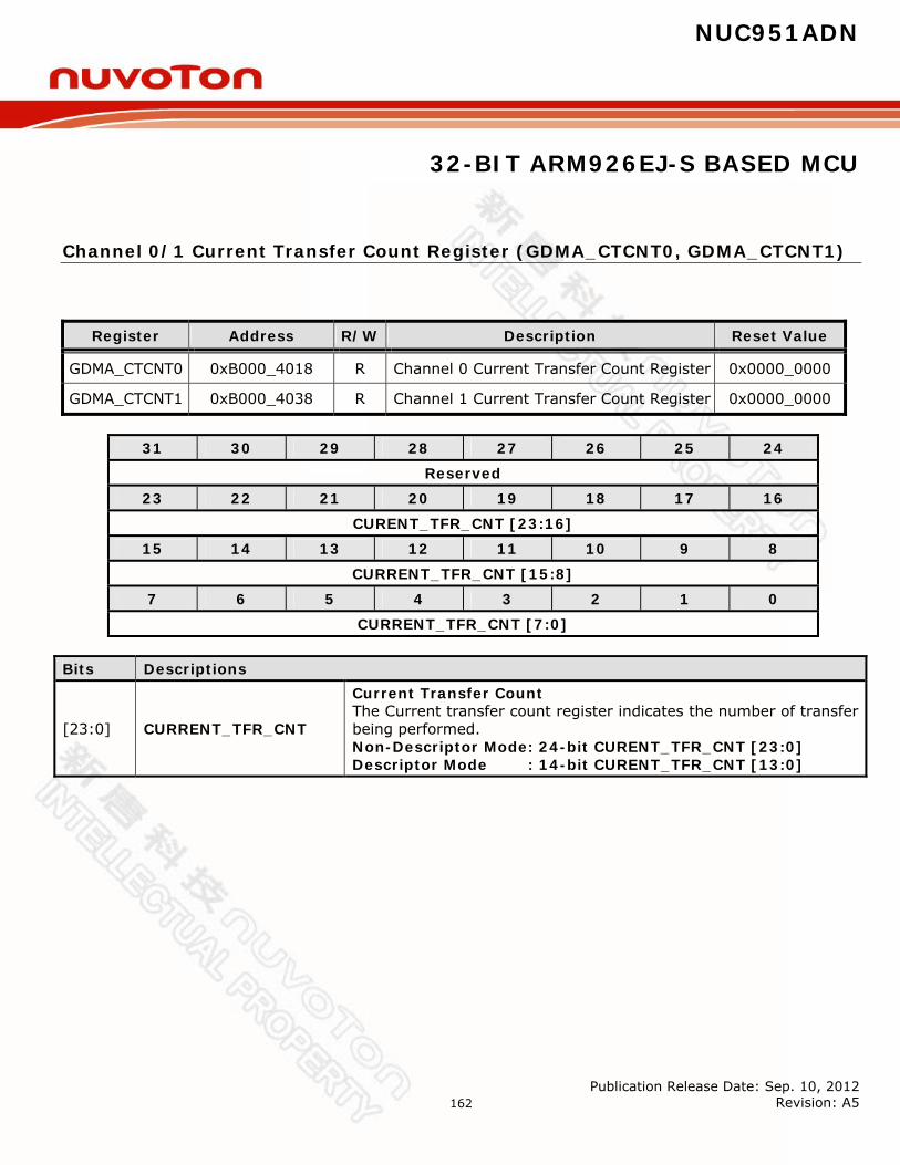
NUC951ADN
32-BIT ARM926EJ-S BASED MCU
Publication Release Date: Sep. 10, 2012 Revision: A5
162
Channel 0/1 Current Transfer Count Register (GDMA_CTCNT0, GDMA_CTCNT1)
Register Address R/W Description Reset Value
GDMA_CTCNT0 0xB000_4018 R Channel 0 Current Transfer Count Register 0x0000_0000
GDMA_CTCNT1 0xB000_4038 R Channel 1 Current Transfer Count Register 0x0000_0000
31 30 29 28 27 26 25 24 Reserved
23 22 21 20 19 18 17 16 CURENT_TFR_CNT [23:16]
15 14 13 12 11 10 9 8 CURRENT_TFR_CNT [15:8]
7 6 5 4 3 2 1 0 CURRENT_TFR_CNT [7:0]
Bits Descriptions
[23:0] CURRENT_TFR_CNT
Current Transfer Count The Current transfer count register indicates the number of transfer being performed. Non-Descriptor Mode: 24-bit CURENT_TFR_CNT [23:0] Descriptor Mode : 14-bit CURENT_TFR_CNT [13:0]
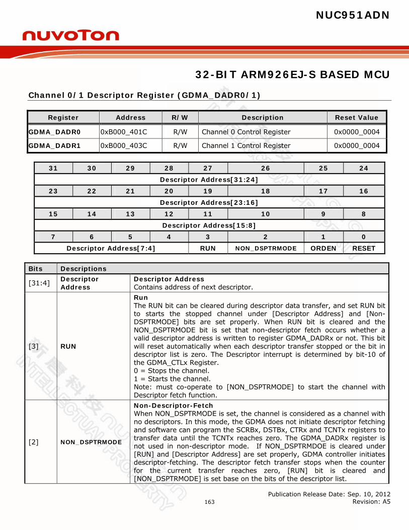
NUC951ADN
32-BIT ARM926EJ-S BASED MCU
Publication Release Date: Sep. 10, 2012 Revision: A5
163
Channel 0/1 Descriptor Register (GDMA_DADR0/1)
Register Address R/W Description Reset Value
GDMA_DADR0 0xB000_401C R/W Channel 0 Control Register 0x0000_0004
GDMA_DADR1 0xB000_403C R/W Channel 1 Control Register 0x0000_0004
31 30 29 28 27 26 25 24
Descriptor Address[31:24] 23 22 21 20 19 18 17 16
Descriptor Address[23:16]
15 14 13 12 11 10 9 8 Descriptor Address[15:8]
7 6 5 4 3 2 1 0 Descriptor Address[7:4] RUN NON_DSPTRMODE ORDEN RESET
Bits Descriptions
[31:4] Descriptor Address
Descriptor Address Contains address of next descriptor.
[3] RUN
Run The RUN bit can be cleared during descriptor data transfer, and set RUN bit to starts the stopped channel under [Descriptor Address] and [Non-DSPTRMODE] bits are set properly. When RUN bit is cleared and the NON_DSPTRMODE bit is set that non-descriptor fetch occurs whether a valid descriptor address is written to register GDMA_DADRx or not. This bit will reset automatically when each descriptor transfer stopped or the bit in descriptor list is zero. The Descriptor interrupt is determined by bit-10 of the GDMA_CTLx Register. 0 = Stops the channel. 1 = Starts the channel. Note: must co-operate to [NON_DSPTRMODE] to start the channel with Descriptor fetch function.
[2] NON_DSPTRMODE
Non-Descriptor-Fetch When NON_DSPTRMODE is set, the channel is considered as a channel with no descriptors. In this mode, the GDMA does not initiate descriptor fetching and software can program the SCRBx, DSTBx, CTRx and TCNTx registers to transfer data until the TCNTx reaches zero. The GDMA_DADRx register is not used in non-descriptor mode. If NON_DSPTRMDOE is cleared under [RUN] and [Descriptor Address] are set properly, GDMA controller initiates descriptor-fetching. The descriptor fetch transfer stops when the counter for the current transfer reaches zero, [RUN] bit is cleared and [NON_DSPTRMODE] is set base on the bits of the descriptor list.

NUC951ADN
32-BIT ARM926EJ-S BASED MCU
Publication Release Date: Sep. 10, 2012 Revision: A5
164
0 = Descriptor-fetch transfer 1 = NON-descriptor-fetch transfer Note: this bit = 1 will disable Descriptor function regardless of the RUN bit is 1 or not.
[1] ORDEN
Enable Ordering Execution for Descriptor List The GDMA_DADRx [ORDEN] determine which the next descriptor address will be fetched. If [ORDEN] is set, the GDMA controller fetches the next descriptor from Current GDMA_DADRx [Descriptor Address] + 16 bytes. If this bit is cleared, GDMA fetches the next descriptor address from the current GDMA_DADRx [Descriptor Address] register. GDMA_DADRx [ORDEN] is relevant only for descriptor-fetch function (GDMA_DADRx [NON_DSPTRMODE] = 0). 0 = Disable descriptor ordering. Fetch the next descriptor from register GDMA_DDADRx [Descriptor Address]. 1 = Enable descriptor ordering.
[0] RESET Reset Channel 0 = Disable channel reset. 1 = Enable channel status reset and disable descriptor based function.

NUC951ADN
32-BIT ARM926EJ-S BASED MCU
Publication Release Date: Sep. 10, 2012 Revision: A5
165
Channel 0/1 GDMA Internal Buffer Register (GDMA_INTBUF0/1)
Software can set the [17-16] bit of GDMA_INTCS to select channels and watch the value which has read from memory.
Register Address R/W Description Reset Value
GDMA_INTBUF0 0xB000_4080 R GDMA Internal Buffer Word 0 0x0000_0000
GDMA_INTBUF1 0xB000_4084 R GDMA Internal Buffer Word 1 0x0000_0000
GDMA_INTBUF2 0xB000_4088 R GDMA Internal Buffer Word 2 0x0000_0000
GDMA_INTBUF3 0xB000_408C R GDMA Internal Buffer Word 3 0x0000_0000
GDMA_INTBUF4 0xB000_4090 R GDMA Internal Buffer Word 4 0x0000_0000
GDMA_INTBUF5 0xB000_4094 R GDMA Internal Buffer Word 5 0x0000_0000
GDMA_INTBUF6 0xB000_4098 R GDMA Internal Buffer Word 6 0x0000_0000
GDMA_INTBUF7 0xB000_409C R GDMA Internal Buffer Word 7 0x0000_0000
31 30 29 28 27 26 25 24
DATA_BUFFER [31:24] 23 22 21 20 19 18 17 16
DATA_BUFFER [23:16]
15 14 13 12 11 10 9 8 DATA_BUFFER [15:8]
7 6 5 4 3 2 1 0 DATA_BUFFER [7:0]
Bits Descriptions
[31:0] DATA_BUFFER
Internal Buffer Register Each channel has its own internal buffer from Word 0 to Word 7. The [17-16] bit of GDMA_INTCS will determine the values of channels mapping to GDMA_INTBUF0~7. NOTE: The GDMA_INTBUF0~7 are available when burst mode used, otherwise, only the GDMA_INTBUF0 available.

NUC951ADN
32-BIT ARM926EJ-S BASED MCU
Publication Release Date: Sep. 10, 2012 Revision: A5
166
Channel 0/1 GDMA Interrupt Control and Status Register (GDMA_INTCS)
Register Address R/W Description Reset Value
GDMA_INTCS 0xB000_40A0 R/W Interrupt Control and Status Register (2 Channels) 0x0000_0000
31 30 29 28 27 26 25 24
RESERVED 23 22 21 20 19 18 17 16
RESERVED BUF_RD_SEL 15 14 13 12 11 10 9 8
RESERVED TERR1F TC1F TERR0F TC0F 7 6 5 4 3 2 1 0
RESERVED TERR1EN TC1EN TERR0EN TC0EN
Bits Descriptions
[17:16] BUF_RD_SEL
Internal Buffer Read Select 00 = Read Internal Buffer for Channel 0 01 = Read Internal Buffer for Channel 1 10 = RESERVED 11 = RESERVED
[11] TERR1F
Channel 1 Transfer Error O = No error occurs 1 = Hardware sets this bit on a GDMA transfer failure This bit will be cleared when write logic 1. Transfer error will generate GDMA interrupt
[10] TC1F
Channel 1 Terminal Count 0 = Channel does not expire 1 = Channel expires; this bit is set only by GDMA hardware, and clear by software to write logic 1. TC1 is the GDMA interrupt flag. TC1 or GDMATERR1 will generate interrupt
[9] TERR0F
Channel 0 Transfer Error O = No error occurs 1 = Hardware sets this bit on a GDMA transfer failure This bit will be cleared when write logic 1. Transfer error will generate GDMA interrupt

NUC951ADN
32-BIT ARM926EJ-S BASED MCU
Publication Release Date: Sep. 10, 2012 Revision: A5
167
[8] TC0F
Channel 0 Terminal Count 0 = Channel does not expire 1 = Channel expires; this bit is set only by GDMA hardware, and clear by software to write logic 1. TC0 is the GDMA interrupt flag. TC0 or GDMATERR0 will generate interrupt
[3] TEER1EN Channel 1 Interrupt Enable for Transfer Error 0 = Disable Interrupt 1 = Enable Interrupt
[2] TC1EN Channel 1 Interrupt Enable for Terminal Count 0 = Disable Interrupt 1 = Enable Interrupt
[1] TEER0EN Channel 0 Interrupt Enable for Transfer Error 0 = Disable Interrupt 1 = Enable Interrupt
[0] TC0EN Channel 0 Interrupt Enable for Terminal Count 0 = Disable Interrupt 1 = Enable Interrupt
NUC951ADN
32-BIT ARM926EJ-S BASED MCU
Publication Release Date: Sep. 10, 2012 Revision: A5
168
7.7 USB Host Controller (USBH)
The Universal Serial Bus (USB) is a fast, bi-directional, isochronous, low-cost, dynamically attachable serial interface standard intended for USB devices. The USB is a 4-wire serial cable bus that supports serial data exchange between a Host Controller and a network of peripheral devices. The attached peripherals share USB bandwidth through a host-scheduled, token-based protocol. Peripherals may be attached, configured, used, and detached, while the host and other peripherals continue operation (i.e. hot plug and unplug is supported). A major design goal of the USB standard was to allow flexible, plug-and-play networks of USB devices. In any USB network, there will be only one host, but there can be many devices and hubs. The USB Host Controller includes the following features Fully compliant with USB Revision 2.0 specification. Enhanced Host Controller Interface (EHCI) Revision 1.0 compatible. Open Host Controller Interface (OHCI) Revision 1.0 compatible. Supports high-speed (480Mbps), full-speed (12Mbps) and low-speed (1.5Mbps) USB devices. Supports Control, Bulk, Interrupt, Isochronous and Split transfers. Integrated a port routing logic to route full/low speed device to OHCI controller. Built-in DMA for real-time data transfer.
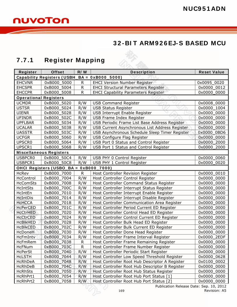
NUC951ADN
32-BIT ARM926EJ-S BASED MCU
Publication Release Date: Sep. 10, 2012 Revision: A5
169
7.7.1 Register Mapping
Register Offset R/W Description Reset Value Capability Registers (USBH_BA = 0xB000_5000) EHCVNR 0xB000_5000 R EHCI Version Number Register 0x0095_0020 EHCSPR 0xB000_5004 R EHCI Structural Parameters Register 0x0000_0012 EHCCPR 0xB000_5008 R EHCI Capability Parameters Register 0x0000_0000 Operational Registers UCMDR 0xB000_5020 R/W USB Command Register 0x0008_0000 USTSR 0xB000_5024 R/W USB Status Register 0x0000_1004 UIENR 0xB000_5028 R/W USB Interrupt Enable Register 0x0000_0000 UFINDR 0xB000_502C R/W USB Frame Index Register 0x0000_0000 UPFLBAR 0xB000_5034 R/W USB Periodic Frame List Base Address Register 0x0000_0000 UCALAR 0xB000_5038 R/W USB Current Asynchronous List Address Register 0x0000_0000 UASSTR 0xB000_503C R/W USB Asynchronous Schedule Sleep Timer Register 0x0000_0BD6 UCFGR 0xB000_5060 R/W USB Configure Flag Register 0x0000_0000 UPSCR0 0xB000_5064 R/W USB Port 0 Status and Control Register 0x0000_2000 UPSCR1 0xB000_5068 R/W USB Port 1 Status and Control Register 0x0000_2000 Miscellaneous Registers USBPCR0 0xB000_50C4 R/W USB PHY 0 Control Register 0x0000_0060 USBPCR1 0xB000_50C8 R/W USB PHY 1 Control Register 0x0000_0020 OHCI Registers (USBO_BA = 0xB000_7000) HcRev 0xB000_7000 R Host Controller Revision Register 0x0000_0010 HcControl 0xB000_7004 R/W Host Controller Control Register 0x0000_0000 HcComSts 0xB000_7008 R/W Host Controller Command Status Register 0x0000_0000 HcIntSts 0xB000_700C R/W Host Controller Interrupt Status Register 0x0000_0000 HcIntEn 0xB000_7010 R/W Host Controller Interrupt Enable Register 0x0000_0000 HcIntDis 0xB000_7014 R/W Host Controller Interrupt Disable Register 0x0000_0000 HcHCCA 0xB000_7018 R/W Host Controller Communication Area Register 0x0000_0000 HcPerCED 0xB000_701C R/W Host Controller Period Current ED Register 0x0000_0000 HcCtrHED 0xB000_7020 R/W Host Controller Control Head ED Register 0x0000_0000 HcCtrCED 0xB000_7024 R/W Host Controller Control Current ED Register 0x0000_0000 HcBlkHED 0xB000_7028 R/W Host Controller Bulk Head ED Register 0x0000_0000 HcBlkCED 0xB000_702C R/W Host Controller Bulk Current ED Register 0x0000_0000 HcDoneH 0xB000_7030 R/W Host Controller Done Head Register 0x0000_0000 HcFmIntv 0xB000_7034 R/W Host Controller Frame Interval Register 0x0000_2EDF HcFmRem 0xB000_7038 R Host Controller Frame Remaining Register 0x0000_0000 HcFNum 0xB000_703C R Host Controller Frame Number Register 0x0000_0000 HcPerSt 0xB000_7040 R/W Host Controller Periodic Start Register 0x0000_0000 HcLSTH 0xB000_7044 R/W Host Controller Low Speed Threshold Register 0x0000_0628 HcRhDeA 0xB000_7048 R/W Host Controller Root Hub Descriptor A Register 0x0100_0002 HcRhDeB 0xB000_704C R/W Host Controller Root Hub Descriptor B Register 0x0000_0000 HcRhSts 0xB000_7050 R/W Host Controller Root Hub Status Register 0x0000_0000 HcRhPrt1 0xB000_7054 R/W Host Controller Root Hub Port Status [1] 0x0000_0000 HcRhPrt2 0xB000_7058 R/W Host Controller Root Hub Port Status [2] 0x0000_0000
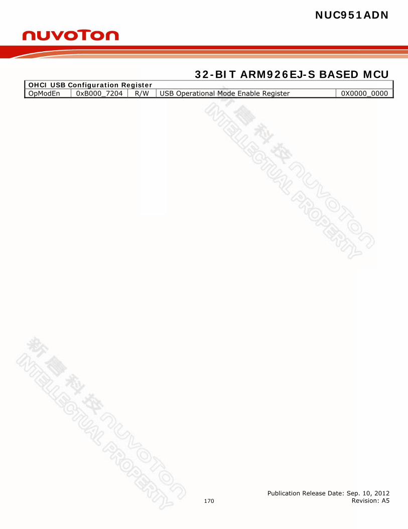
NUC951ADN
32-BIT ARM926EJ-S BASED MCU
Publication Release Date: Sep. 10, 2012 Revision: A5
170
OHCI USB Configuration Register OpModEn 0xB000_7204 R/W USB Operational Mode Enable Register 0X0000_0000

NUC951ADN
32-BIT ARM926EJ-S BASED MCU
Publication Release Date: Sep. 10, 2012 Revision: A5
171
7.7.2 Register Details
EHCI Version Number Register (EHCVNR)
Register Address R/W Description Reset Value EHCVNR 0xB000_5000 R EHCI Version Number Register 0x0095_0020
31 30 29 28 27 26 25 24 Version
23 22 21 20 19 18 17 16 Version
15 14 13 12 11 10 9 8 Reserved
7 6 5 4 3 2 1 0 CR_Length
Bits Descriptions
[31:16] Version
Host Controller Interface Version Number This is a two-byte register containing a BCD encoding of the EHCI revision number supported by this host controller. The most significant byte of this register represents a major revision and the least significant byte is the minor revision.
[7:0] CR_Length Capability Registers Length This register is used as an offset to add to register base to find the beginning of the Operational Register Space.

NUC951ADN
32-BIT ARM926EJ-S BASED MCU
Publication Release Date: Sep. 10, 2012 Revision: A5
172
EHCI Structural Parameters Register (EHCSPR)
Register Address R/W Description Reset Value EHCSPR 0xB000_5004 R EHCI Structural Parameters Register 0x0000_0012
31 30 29 28 27 26 25 24 Reserved
23 22 21 20 19 18 17 16 Reserved
15 14 13 12 11 10 9 8 N_CC N_PCC
7 6 5 4 3 2 1 0 Reserved PPC N_PORTS
Bits Descriptions
[15:12] N_CC
Number of Companion Controller This field indicates the number of companion controllers associated with this USB 2.0 host controller. A zero in this field indicates there are no companion host controllers. Port-ownership hand-off is not supported. Only high-speed devices are supported on the host controller root ports. A value larger than zero in this field indicates there are companion USB 1.1 host controller(s). Port-ownership hand-offs are supported. High, Full- and Low-speed devices are supported on the host controller root ports.
[11:8] N_PCC
Number of Ports per Companion Controller This field indicates the number of ports supported per companion host controller. It is used to indicate the port routing configuration to system software. For example, if N_PORTS has a value of 6 and N_CC has a value of 2 then N_PCC could have a value of 3. The convention is that the first N_PCC ports are assumed to be routed to companion controller 1, the next N_PCC ports to companion controller 2, etc. In the previous example, the N_PCC could have been 4, where the first 4 are routed to companion controller 1 and the last two are routed to companion controller 2. The number in this field must be consistent with N_PORTS and N_CC.
[4] PPC
Port Power Control This field indicates whether the host controller implementation includes port power control. A one in this bit indicates the ports have port power switches. A zero in this bit indicates the port do not have port power stitches. The value of this field affects the functionality of the Port Power field in each port status and control register.
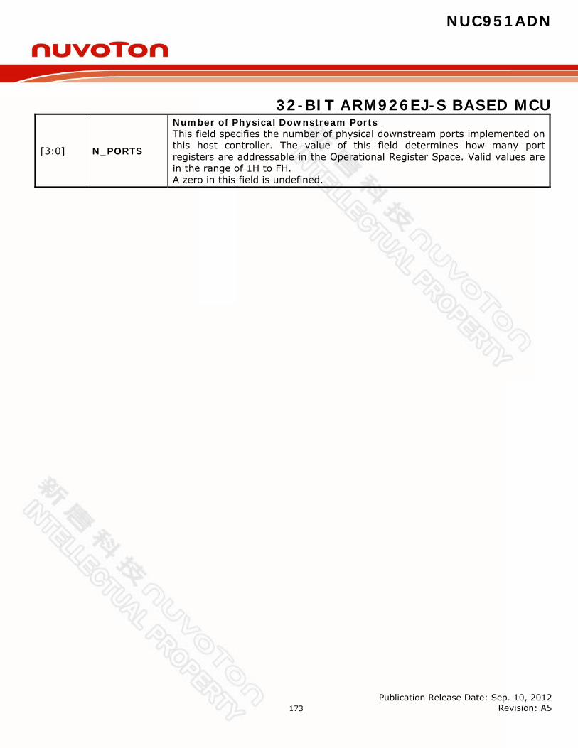
NUC951ADN
32-BIT ARM926EJ-S BASED MCU
Publication Release Date: Sep. 10, 2012 Revision: A5
173
[3:0] N_PORTS
Number of Physical Downstream Ports This field specifies the number of physical downstream ports implemented on this host controller. The value of this field determines how many port registers are addressable in the Operational Register Space. Valid values are in the range of 1H to FH. A zero in this field is undefined.
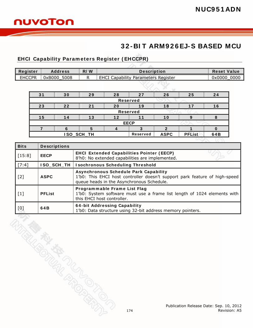
NUC951ADN
32-BIT ARM926EJ-S BASED MCU
Publication Release Date: Sep. 10, 2012 Revision: A5
174
EHCI Capability Parameters Register (EHCCPR)
Register Address R/W Description Reset Value EHCCPR 0xB000_5008 R EHCI Capability Parameters Register 0x0000_0000
31 30 29 28 27 26 25 24 Reserved
23 22 21 20 19 18 17 16 Reserved
15 14 13 12 11 10 9 8 EECP
7 6 5 4 3 2 1 0 ISO_SCH_TH Reserved ASPC PFList 64B
Bits Descriptions
[15:8] EECP EHCI Extended Capabilities Pointer (EECP) 8’h0: No extended capabilities are implemented.
[7:4] ISO_SCH_TH Isochronous Scheduling Threshold
[2] ASPC Asynchronous Schedule Park Capability 1’b0: This EHCI host controller doesn’t support park feature of high-speed queue heads in the Asynchronous Schedule.
[1] PFList Programmable Frame List Flag 1’b0: System software must use a frame list length of 1024 elements with this EHCI host controller.
[0] 64B 64-bit Addressing Capability 1’b0: Data structure using 32-bit address memory pointers.
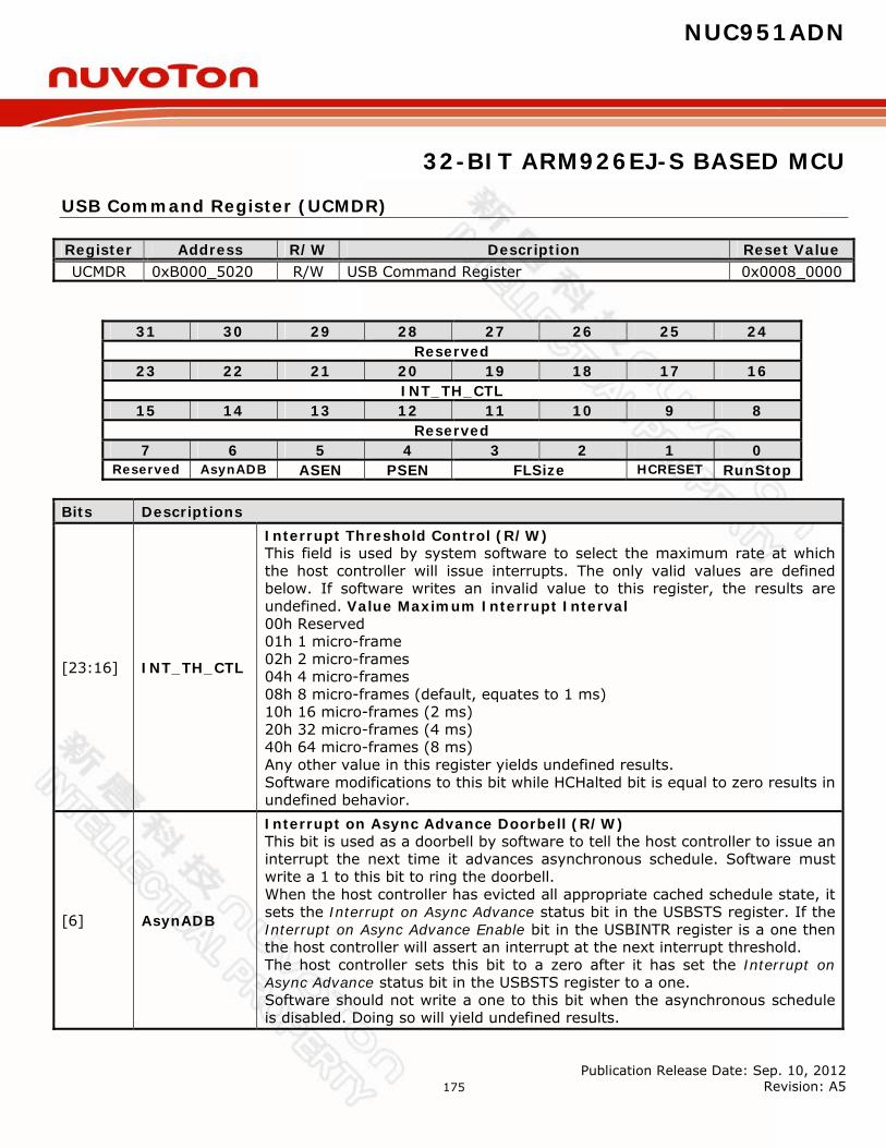
NUC951ADN
32-BIT ARM926EJ-S BASED MCU
Publication Release Date: Sep. 10, 2012 Revision: A5
175
USB Command Register (UCMDR)
Register Address R/W Description Reset Value UCMDR 0xB000_5020 R/W USB Command Register 0x0008_0000
31 30 29 28 27 26 25 24 Reserved
23 22 21 20 19 18 17 16 INT_TH_CTL
15 14 13 12 11 10 9 8 Reserved
7 6 5 4 3 2 1 0 Reserved AsynADB ASEN PSEN FLSize HCRESET RunStop
Bits Descriptions
[23:16] INT_TH_CTL
Interrupt Threshold Control (R/W) This field is used by system software to select the maximum rate at which the host controller will issue interrupts. The only valid values are defined below. If software writes an invalid value to this register, the results are undefined. Value Maximum Interrupt Interval 00h Reserved 01h 1 micro-frame 02h 2 micro-frames 04h 4 micro-frames 08h 8 micro-frames (default, equates to 1 ms) 10h 16 micro-frames (2 ms) 20h 32 micro-frames (4 ms) 40h 64 micro-frames (8 ms) Any other value in this register yields undefined results. Software modifications to this bit while HCHalted bit is equal to zero results in undefined behavior.
[6] AsynADB
Interrupt on Async Advance Doorbell (R/W) This bit is used as a doorbell by software to tell the host controller to issue an interrupt the next time it advances asynchronous schedule. Software must write a 1 to this bit to ring the doorbell. When the host controller has evicted all appropriate cached schedule state, it sets the Interrupt on Async Advance status bit in the USBSTS register. If the Interrupt on Async Advance Enable bit in the USBINTR register is a one then the host controller will assert an interrupt at the next interrupt threshold. The host controller sets this bit to a zero after it has set the Interrupt on Async Advance status bit in the USBSTS register to a one. Software should not write a one to this bit when the asynchronous schedule is disabled. Doing so will yield undefined results.
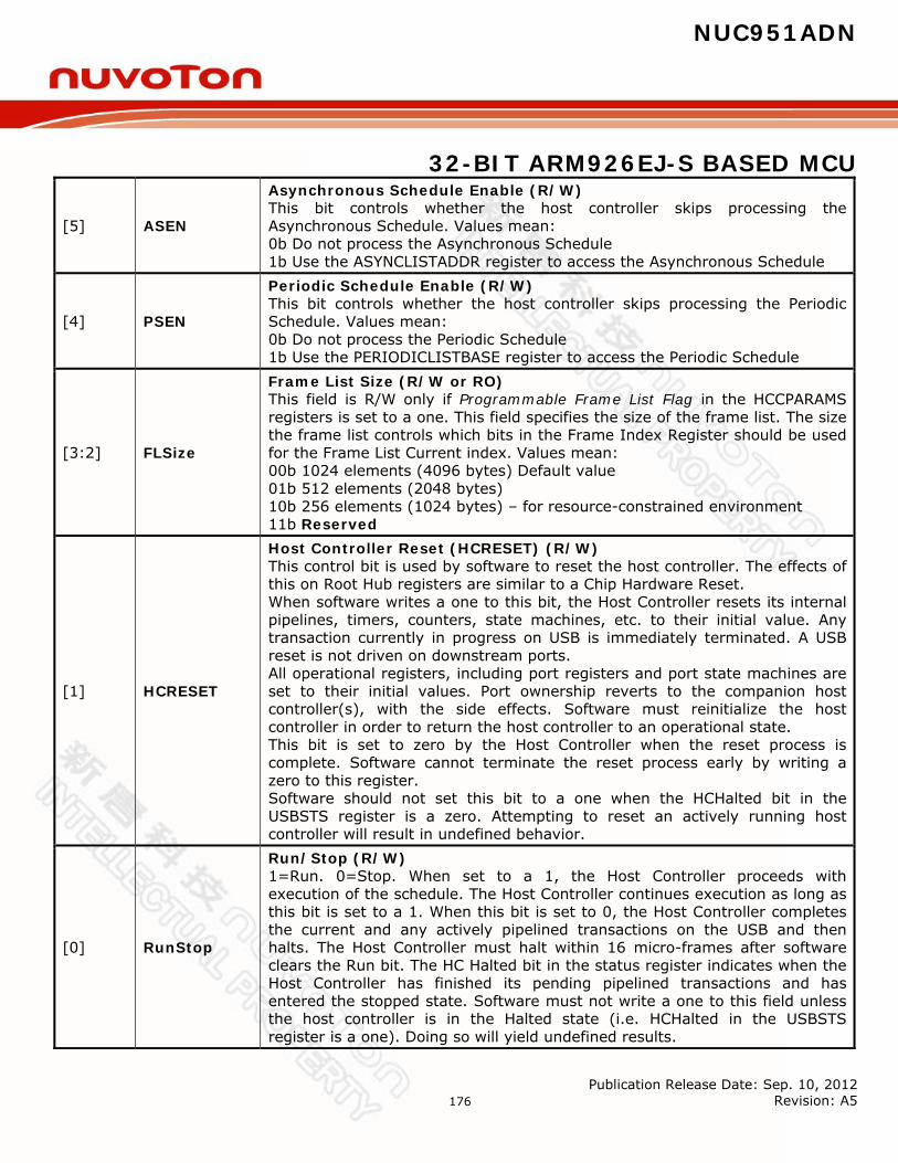
NUC951ADN
32-BIT ARM926EJ-S BASED MCU
Publication Release Date: Sep. 10, 2012 Revision: A5
176
[5] ASEN
Asynchronous Schedule Enable (R/W) This bit controls whether the host controller skips processing the Asynchronous Schedule. Values mean: 0b Do not process the Asynchronous Schedule 1b Use the ASYNCLISTADDR register to access the Asynchronous Schedule
[4] PSEN
Periodic Schedule Enable (R/W) This bit controls whether the host controller skips processing the Periodic Schedule. Values mean: 0b Do not process the Periodic Schedule 1b Use the PERIODICLISTBASE register to access the Periodic Schedule
[3:2] FLSize
Frame List Size (R/W or RO) This field is R/W only if Programmable Frame List Flag in the HCCPARAMS registers is set to a one. This field specifies the size of the frame list. The size the frame list controls which bits in the Frame Index Register should be used for the Frame List Current index. Values mean: 00b 1024 elements (4096 bytes) Default value 01b 512 elements (2048 bytes) 10b 256 elements (1024 bytes) – for resource-constrained environment 11b Reserved
[1] HCRESET
Host Controller Reset (HCRESET) (R/W) This control bit is used by software to reset the host controller. The effects of this on Root Hub registers are similar to a Chip Hardware Reset. When software writes a one to this bit, the Host Controller resets its internal pipelines, timers, counters, state machines, etc. to their initial value. Any transaction currently in progress on USB is immediately terminated. A USB reset is not driven on downstream ports. All operational registers, including port registers and port state machines are set to their initial values. Port ownership reverts to the companion host controller(s), with the side effects. Software must reinitialize the host controller in order to return the host controller to an operational state. This bit is set to zero by the Host Controller when the reset process is complete. Software cannot terminate the reset process early by writing a zero to this register. Software should not set this bit to a one when the HCHalted bit in the USBSTS register is a zero. Attempting to reset an actively running host controller will result in undefined behavior.
[0] RunStop
Run/Stop (R/W) 1=Run. 0=Stop. When set to a 1, the Host Controller proceeds with execution of the schedule. The Host Controller continues execution as long as this bit is set to a 1. When this bit is set to 0, the Host Controller completes the current and any actively pipelined transactions on the USB and then halts. The Host Controller must halt within 16 micro-frames after software clears the Run bit. The HC Halted bit in the status register indicates when the Host Controller has finished its pending pipelined transactions and has entered the stopped state. Software must not write a one to this field unless the host controller is in the Halted state (i.e. HCHalted in the USBSTS register is a one). Doing so will yield undefined results.
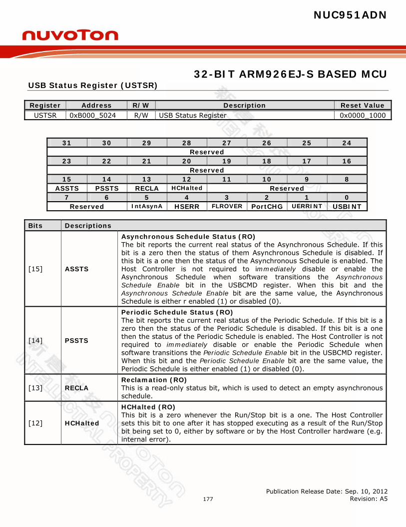
NUC951ADN
32-BIT ARM926EJ-S BASED MCU
Publication Release Date: Sep. 10, 2012 Revision: A5
177
USB Status Register (USTSR)
Register Address R/W Description Reset Value USTSR 0xB000_5024 R/W USB Status Register 0x0000_1000
31 30 29 28 27 26 25 24 Reserved
23 22 21 20 19 18 17 16 Reserved
15 14 13 12 11 10 9 8 ASSTS PSSTS RECLA HCHalted Reserved
7 6 5 4 3 2 1 0 Reserved IntAsynA HSERR FLROVER PortCHG UERRINT USBINT
Bits Descriptions
[15] ASSTS
Asynchronous Schedule Status (RO) The bit reports the current real status of the Asynchronous Schedule. If this bit is a zero then the status of them Asynchronous Schedule is disabled. If this bit is a one then the status of the Asynchronous Schedule is enabled. The Host Controller is not required to immediately disable or enable the Asynchronous Schedule when software transitions the Asynchronous Schedule Enable bit in the USBCMD register. When this bit and the Asynchronous Schedule Enable bit are the same value, the Asynchronous Schedule is either r enabled (1) or disabled (0).
[14] PSSTS
Periodic Schedule Status (RO) The bit reports the current real status of the Periodic Schedule. If this bit is a zero then the status of the Periodic Schedule is disabled. If this bit is a one then the status of the Periodic Schedule is enabled. The Host Controller is not required to immediately disable or enable the Periodic Schedule when software transitions the Periodic Schedule Enable bit in the USBCMD register. When this bit and the Periodic Schedule Enable bit are the same value, the Periodic Schedule is either enabled (1) or disabled (0).
[13] RECLA Reclamation (RO) This is a read-only status bit, which is used to detect an empty asynchronous schedule.
[12] HCHalted
HCHalted (RO) This bit is a zero whenever the Run/Stop bit is a one. The Host Controller sets this bit to one after it has stopped executing as a result of the Run/Stop bit being set to 0, either by software or by the Host Controller hardware (e.g. internal error).

NUC951ADN
32-BIT ARM926EJ-S BASED MCU
Publication Release Date: Sep. 10, 2012 Revision: A5
178
[5] IntAsynA
Interrupt on Async Advance (R/WC) System software can force the host controller to issue an interrupt the next time the host controller advances the asynchronous schedule by writing a one to the Interrupt on Async Advance Doorbell bit in the USBCMD register. This status bit indicates the assertion of that interrupt source.
[4] HSERR Host System Error (R/WC) The Host Controller sets this bit to 1 when a serious error occurs during a host system access involving the Host Controller module.
[3] FLROVER
Frame List Rollover (R/WC) The Host Controller sets this bit to a one when the Frame List Index rolls over from its maximum value to zero. The exact value at which the rollover occurs depends on the frame list size. For example, if the frame list size (as programmed in the Frame List Size field of the USBCMD register) is 1024, the Frame Index Register rolls over every time FRINDEX [13] toggles. Similarly, if the size is 512, the Host Controller sets this bit to a one every time FRINDEX [12] toggles.
[2] PortCHG
Port Change Detect (R/WC) The Host Controller sets this bit to a one when any port for which the Port Owner bit is set to zero has a change bit transition from a zero to a one or a Force Port Resume bit transition from a zero to a one as a result of a J-K transition detected on a suspended port. This bit will also be set as a result of the Connect Status Change being set to a one after system software has relinquished ownership of a connected port by writing a one to a port's Port Owner bit. This bit is allowed to be maintained in the Auxiliary power well. Alternatively, it is also acceptable that on a D3 to D0 transition of the EHCI HC device, this bit is loaded with the OR of all of the PORTSC change bits (including: Force port resume, over-current change, enable/disable change and connect status change).
[1] UERRINT
USB Error Interrupt (USBERRINT) (R/WC) The Host Controller sets this bit to 1 when completion of a USB transaction results in an error condition (e.g., error counter underflow). If the TD on which the error interrupt occurred also had its IOC bit set, both this bit and USBINT bit are set.
[0] USBINT
USB Interrupt (USBINT) (R/WC) The Host Controller sets this bit to 1 on the completion of a USB transaction, which results in the retirement of a Transfer Descriptor that had its IOC bit set. The Host Controller also sets this bit to 1 when a short packet is detected (actual number of bytes received was less than the expected number of bytes).
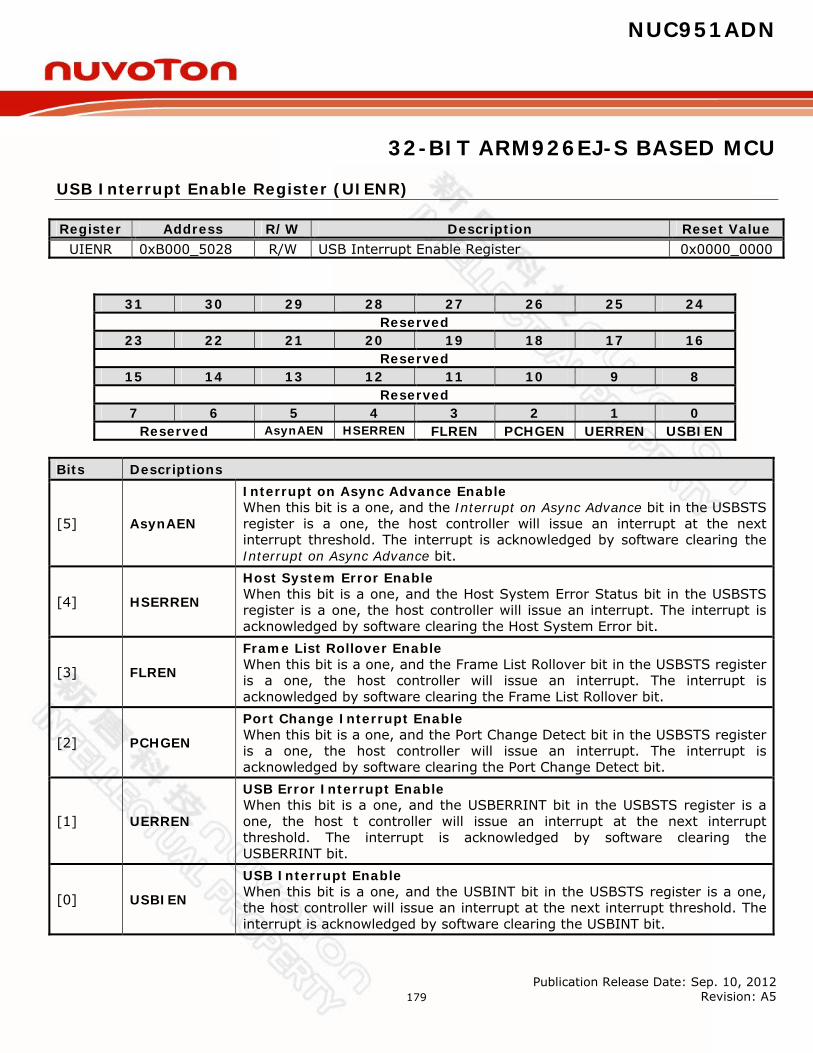
NUC951ADN
32-BIT ARM926EJ-S BASED MCU
Publication Release Date: Sep. 10, 2012 Revision: A5
179
USB Interrupt Enable Register (UIENR)
Register Address R/W Description Reset Value UIENR 0xB000_5028 R/W USB Interrupt Enable Register 0x0000_0000
31 30 29 28 27 26 25 24 Reserved
23 22 21 20 19 18 17 16 Reserved
15 14 13 12 11 10 9 8 Reserved
7 6 5 4 3 2 1 0 Reserved AsynAEN HSERREN FLREN PCHGEN UERREN USBIEN
Bits Descriptions
[5] AsynAEN
Interrupt on Async Advance Enable When this bit is a one, and the Interrupt on Async Advance bit in the USBSTS register is a one, the host controller will issue an interrupt at the next interrupt threshold. The interrupt is acknowledged by software clearing the Interrupt on Async Advance bit.
[4] HSERREN
Host System Error Enable When this bit is a one, and the Host System Error Status bit in the USBSTS register is a one, the host controller will issue an interrupt. The interrupt is acknowledged by software clearing the Host System Error bit.
[3] FLREN
Frame List Rollover Enable When this bit is a one, and the Frame List Rollover bit in the USBSTS register is a one, the host controller will issue an interrupt. The interrupt is acknowledged by software clearing the Frame List Rollover bit.
[2] PCHGEN
Port Change Interrupt Enable When this bit is a one, and the Port Change Detect bit in the USBSTS register is a one, the host controller will issue an interrupt. The interrupt is acknowledged by software clearing the Port Change Detect bit.
[1] UERREN
USB Error Interrupt Enable When this bit is a one, and the USBERRINT bit in the USBSTS register is a one, the host t controller will issue an interrupt at the next interrupt threshold. The interrupt is acknowledged by software clearing the USBERRINT bit.
[0] USBIEN
USB Interrupt Enable When this bit is a one, and the USBINT bit in the USBSTS register is a one, the host controller will issue an interrupt at the next interrupt threshold. The interrupt is acknowledged by software clearing the USBINT bit.
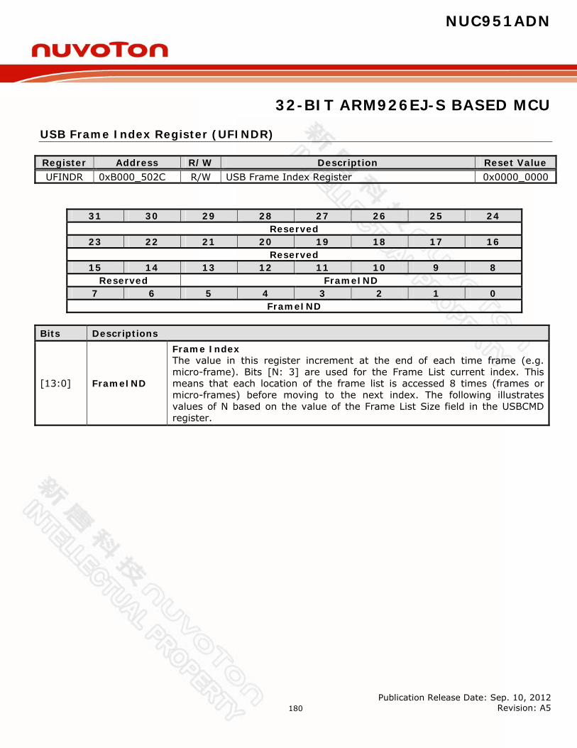
NUC951ADN
32-BIT ARM926EJ-S BASED MCU
Publication Release Date: Sep. 10, 2012 Revision: A5
180
USB Frame Index Register (UFINDR)
Register Address R/W Description Reset Value UFINDR 0xB000_502C R/W USB Frame Index Register 0x0000_0000
31 30 29 28 27 26 25 24 Reserved
23 22 21 20 19 18 17 16 Reserved
15 14 13 12 11 10 9 8 Reserved FrameIND
7 6 5 4 3 2 1 0 FrameIND
Bits Descriptions
[13:0] FrameIND
Frame Index The value in this register increment at the end of each time frame (e.g. micro-frame). Bits [N: 3] are used for the Frame List current index. This means that each location of the frame list is accessed 8 times (frames or micro-frames) before moving to the next index. The following illustrates values of N based on the value of the Frame List Size field in the USBCMD register.

NUC951ADN
32-BIT ARM926EJ-S BASED MCU
Publication Release Date: Sep. 10, 2012 Revision: A5
181
USB Periodic Frame List Base Address Register (UPFLBAR)
Register Address R/W Description Reset Value UPFLBAR 0xB000_5034 R/W USB Periodic Frame List Base Address Register 0x0000_0000
31 30 29 28 27 26 25 24 BADDR
23 22 21 20 19 18 17 16 BADDR
15 14 13 12 11 10 9 8 BADDR Reserved
7 6 5 4 3 2 1 0 Reserved
Bits Descriptions
[31:12] BADDR Base Address (Low) These bits correspond to memory address signals [31:12], respectively.
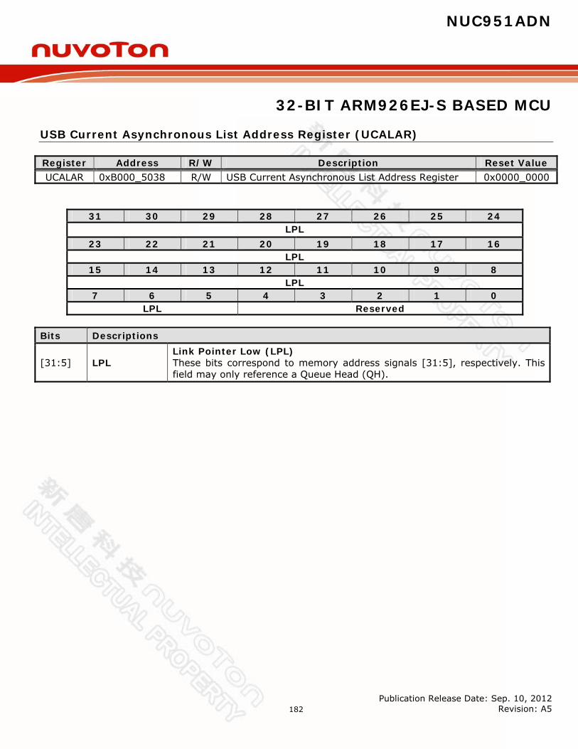
NUC951ADN
32-BIT ARM926EJ-S BASED MCU
Publication Release Date: Sep. 10, 2012 Revision: A5
182
USB Current Asynchronous List Address Register (UCALAR)
Register Address R/W Description Reset Value UCALAR 0xB000_5038 R/W USB Current Asynchronous List Address Register 0x0000_0000
31 30 29 28 27 26 25 24 LPL
23 22 21 20 19 18 17 16 LPL
15 14 13 12 11 10 9 8 LPL
7 6 5 4 3 2 1 0 LPL Reserved
Bits Descriptions
[31:5] LPL Link Pointer Low (LPL) These bits correspond to memory address signals [31:5], respectively. This field may only reference a Queue Head (QH).

NUC951ADN
32-BIT ARM926EJ-S BASED MCU
Publication Release Date: Sep. 10, 2012 Revision: A5
183
USB Asynchronous Schedule Sleep Timer Register
Register Address R/W Description Reset Value UASSTR 0xB000_503C R/W USB Asynchronous Schedule Sleep Timer Register 0x0000_0BD6
31 30 29 28 27 26 25 24 Reserved
23 22 21 20 19 18 17 16 Reserved
15 14 13 12 11 10 9 8 Reserved ASTMR
7 6 5 4 3 2 1 0 ASTMR
Bits Descriptions
[11:0] ASSTMR
Asynchronous Schedule Sleep Timer This field defines the AsyncSchedSleepTime of EHCI spec. The asynchronous schedule sleep timer is used to control how often the host controller fetches asynchronous schedule list from system memory while the asynchronous schedule is empty. The default value of this timer is 12’hBD6. Because this timer is implemented in UTMI clock (30MHz) domain, the default sleeping time will be about 100us.
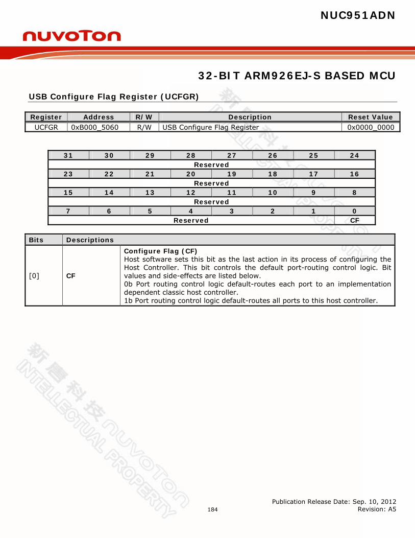
NUC951ADN
32-BIT ARM926EJ-S BASED MCU
Publication Release Date: Sep. 10, 2012 Revision: A5
184
USB Configure Flag Register (UCFGR)
Register Address R/W Description Reset Value UCFGR 0xB000_5060 R/W USB Configure Flag Register 0x0000_0000
31 30 29 28 27 26 25 24 Reserved
23 22 21 20 19 18 17 16 Reserved
15 14 13 12 11 10 9 8 Reserved
7 6 5 4 3 2 1 0 Reserved CF
Bits Descriptions
[0] CF
Configure Flag (CF) Host software sets this bit as the last action in its process of configuring the Host Controller. This bit controls the default port-routing control logic. Bit values and side-effects are listed below. 0b Port routing control logic default-routes each port to an implementation dependent classic host controller. 1b Port routing control logic default-routes all ports to this host controller.
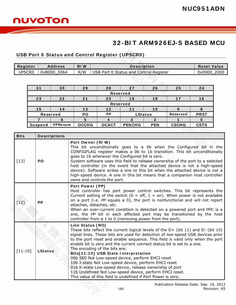
NUC951ADN
32-BIT ARM926EJ-S BASED MCU
Publication Release Date: Sep. 10, 2012 Revision: A5
185
USB Port 0 Status and Control Register (UPSCR0)
Register Address R/W Description Reset Value UPSCR0 0xB000_5064 R/W USB Port 0 Status and Control Register 0x0000_2000
31 30 29 28 27 26 25 24 Reserved
23 22 21 20 19 18 17 16 Reserved
15 14 13 12 11 10 9 8 Reserved PO PP LStatus Reserved PRST
7 6 5 4 3 2 1 0 Suspend FPResum OCCHG OCACT PENCHG PEN CSCHG CSTS
Bits Descriptions
[13] PO
Port Owner (R/W) This bit unconditionally goes to a 0b when the Configured bit in the CONFIGFLAG register makes a 0b to 1b transition. This bit unconditionally goes to 1b whenever the Configured bit is zero. System software uses this field to release ownership of the port to a selected host controller (in the event that the attached device is not a high-speed device). Software writes a one to this bit when the attached device is not a high-speed device. A one in this bit means that a companion host controller owns and controls the port.
[12] PP
Port Power (PP) Host controller has port power control switches. This bit represents the Current setting of the switch (0 = off, 1 = on). When power is not available on a port (i.e. PP equals a 0), the port is nonfunctional and will not report attaches, detaches, etc. When an over-current condition is detected on a powered port and PPC is a one, the PP bit in each affected port may be transitioned by the host controller from a 1 to 0 (removing power from the port).
[11:10] LStatus
Line Status (RO) These bits reflect the current logical levels of the D+ (bit 11) and D- (bit 10) signal lines. These bits are used for detection of low-speed USB devices prior to the port reset and enable sequence. This field is valid only when the port enable bit is zero and the current connect status bit is set to a one. The encoding of the bits are: Bits[11:10] USB State Interpretation 00b SE0 Not Low-speed device, perform EHCI reset 10b J-state Not Low-speed device, perform EHCI reset 01b K-state Low-speed device, release ownership of port 11b Undefined Not Low-speed device, perform EHCI reset. This value of this field is undefined if Port Power is zero.
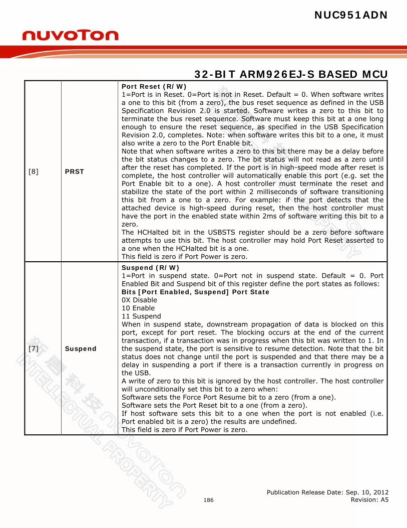
NUC951ADN
32-BIT ARM926EJ-S BASED MCU
Publication Release Date: Sep. 10, 2012 Revision: A5
186
[8] PRST
Port Reset (R/W) 1=Port is in Reset. 0=Port is not in Reset. Default = 0. When software writes a one to this bit (from a zero), the bus reset sequence as defined in the USB Specification Revision 2.0 is started. Software writes a zero to this bit to terminate the bus reset sequence. Software must keep this bit at a one long enough to ensure the reset sequence, as specified in the USB Specification Revision 2.0, completes. Note: when software writes this bit to a one, it must also write a zero to the Port Enable bit. Note that when software writes a zero to this bit there may be a delay before the bit status changes to a zero. The bit status will not read as a zero until after the reset has completed. If the port is in high-speed mode after reset is complete, the host controller will automatically enable this port (e.g. set the Port Enable bit to a one). A host controller must terminate the reset and stabilize the state of the port within 2 milliseconds of software transitioning this bit from a one to a zero. For example: if the port detects that the attached device is high-speed during reset, then the host controller must have the port in the enabled state within 2ms of software writing this bit to a zero. The HCHalted bit in the USBSTS register should be a zero before software attempts to use this bit. The host controller may hold Port Reset asserted to a one when the HCHalted bit is a one. This field is zero if Port Power is zero.
[7] Suspend
Suspend (R/W) 1=Port in suspend state. 0=Port not in suspend state. Default = 0. Port Enabled Bit and Suspend bit of this register define the port states as follows: Bits [Port Enabled, Suspend] Port State 0X Disable 10 Enable 11 Suspend When in suspend state, downstream propagation of data is blocked on this port, except for port reset. The blocking occurs at the end of the current transaction, if a transaction was in progress when this bit was written to 1. In the suspend state, the port is sensitive to resume detection. Note that the bit status does not change until the port is suspended and that there may be a delay in suspending a port if there is a transaction currently in progress on the USB. A write of zero to this bit is ignored by the host controller. The host controller will unconditionally set this bit to a zero when: Software sets the Force Port Resume bit to a zero (from a one). Software sets the Port Reset bit to a one (from a zero). If host software sets this bit to a one when the port is not enabled (i.e. Port enabled bit is a zero) the results are undefined. This field is zero if Port Power is zero.

NUC951ADN
32-BIT ARM926EJ-S BASED MCU
Publication Release Date: Sep. 10, 2012 Revision: A5
187
[6] FPResum
Force Port Resume (R/W) 1= Resume detected/driven on port. 0=No resume (Kstate) detected/driven on port. Default = 0. This functionality defined for manipulating this bit depends on the value of the Suspend bit. For example, if the port is not suspended (Suspend and Enabled bits are a one) and software transitions this bit to a one, then the effects on the bus are undefined. Software sets this bit to a 1 to drive resume signaling. The Host Controller sets this bit to a 1 if a J-to-K transition is detected while the port is in the Suspend state. When this bit transitions to a one because a J-to-K transition is detected, the Port Change Detect bit in the USBSTS register is also set to a one. If software sets this bit to a one, the host controller must not set the Port Change Detect bit. Note that when the EHCI controller owns the port, the resume sequence follows the defined sequence documented in the USB Specification Revision 2.0. The resume signaling (Full-speed 'K') is driven on the port as long as this bit remains a one. Software must appropriately time the Resume and set this bit to a zero when the appropriate amount of time has elapsed. Writing a zero (from one) causes the port to return to high-speed mode (forcing the bus below the port into a high-speed idle). This bit will remain a one until the port has switched to the high-speed idle. The host controller must complete this transition within 2 milliseconds of software setting this bit to a zero. This field is zero if Port Power is zero.
[5] OCCHG Over-current Change (R/WC) Default = 0. 1=This bit gets set to a one when there is a change to Over-current Active. Software clears this bit by writing a one to this bit position.
[4] OCACT
Over-current Active (RO) Default = 0. 1=This port currently has an over current condition. 0=This port does not have an over-current condition. This bit will automatically transition from a one to a zero when the over current condition is removed.
[3] PENCHG
Port Enable/Disable Change (R/WC) 1=Port enabled/disabled status has changed. 0=No change. Default = 0. For the root hub, this bit gets set to a one only when a port is disabled due to the appropriate conditions existing at the EOF2 point (See Chapter 11 of the USB Specification for the definition of a Port Error). Software clears this bit by writing a 1 to it. This field is zero if Port Power is zero.

NUC951ADN
32-BIT ARM926EJ-S BASED MCU
Publication Release Date: Sep. 10, 2012 Revision: A5
188
[2] PEN
Port Enabled/Disabled (R/W) 1=Enable. 0=Disable. Default = 0. Ports can only be enabled by the host controller as a part of the reset and enable. Software cannot enable a port by writing a one to this field. The host controller will only set this bit to a one when the reset sequence determines that the attached device is a high-speed device. Ports can be disabled by either a fault condition (disconnect event or other fault condition) or by host software. Note that the bit status does not change until the port state actually changes. There may be a delay in disabling or enabling a port due to other host controller and bus events. When the port is disabled (0b) downstream propagation of data is blocked on this port, except for reset. This field is zero if Port Power is zero.
[1] CSCHG
Connect Status Change (R/W) 1=Change in Current Connect Status. 0=No change. Default = 0. Indicates a change has occurred in the port’s Current Connect Status. The host controller sets this bit for all changes to the port device connect status, even if system software has not cleared an existing connect status change. For example, the insertion status changes twice before system software has cleared the changed condition, hub hardware will be “setting” an already-set bit (i.e., the bit will remain set).Software sets this bit to 0 by writing a 1 to it. This field is zero if Port Power is zero.
[0] CSTS
Current Connect Status (RO) 1=Device is present on port. 0=No device is present. Default = 0. This value reflects the current state of the port, and may not correspond directly to the event that caused the Connect Status Change bit (Bit 1) to be set. This field is zero if Port Power is zero.

NUC951ADN
32-BIT ARM926EJ-S BASED MCU
Publication Release Date: Sep. 10, 2012 Revision: A5
189
USB Port 1 Status and Control Register (UPSCR1)
Register Address R/W Description Reset Value UPSCR1 0xB000_5068 R/W USB Port 1 Status and Control Register 0x0000_2000
31 30 29 28 27 26 25 24 Reserved
23 22 21 20 19 18 17 16 Reserved Reserved
15 14 13 12 11 10 9 8 Reserved PO PP LStatus Reserved PRST
7 6 5 4 3 2 1 0 Suspend FPResum OCCHG OCACT PENCHG PEN CSCHG CSTS
Bits Descriptions
[13] PO
Port Owner (R/W) This bit unconditionally goes to a 0b when the Configured bit in the CONFIGFLAG register makes a 0b to 1b transition. This bit unconditionally goes to 1b whenever the Configured bit is zero. System software uses this field to release ownership of the port to a selected host controller (in the event that the attached device is not a high-speed device). Software writes a one to this bit when the attached device is not a high-speed device. A one in this bit means that a companion host controller owns and controls the port.
[12] PP
Port Power (PP) Host controller has port power control switches. This bit represents the Current setting of the switch (0 = off, 1 = on). When power is not available on a port (i.e. PP equals a 0), the port is nonfunctional and will not report attaches, detaches, etc. When an over-current condition is detected on a powered port and PPC is a one, the PP bit in each affected port may be transitioned by the host controller from a 1 to 0 (removing power from the port).
[11:10] LStatus
Line Status (RO) These bits reflect the current logical levels of the D+ (bit 11) and D- (bit 10) signal lines. These bits are used for detection of low-speed USB devices prior to the port reset and enable sequence. This field is valid only when the port enable bit is zero and the current connect status bit is set to a one. The encoding of the bits are: Bits[11:10] USB State Interpretation 00b SE0 Not Low-speed device, perform EHCI reset 10b J-state Not Low-speed device, perform EHCI reset 01b K-state Low-speed device, release ownership of port 11b Undefined Not Low-speed device, perform EHCI reset. This value of this field is undefined if Port Power is zero.

NUC951ADN
32-BIT ARM926EJ-S BASED MCU
Publication Release Date: Sep. 10, 2012 Revision: A5
190
[8] PRST
Port Reset (R/W) 1=Port is in Reset. 0=Port is not in Reset. Default = 0. When software writes a one to this bit (from a zero), the bus reset sequence as defined in the USB Specification Revision 2.0 is started. Software writes a zero to this bit to terminate the bus reset sequence. Software must keep this bit at a one long enough to ensure the reset sequence, as specified in the USB Specification Revision 2.0, completes. Note: when software writes this bit to a one, it must also write a zero to the Port Enable bit. Note that when software writes a zero to this bit there may be a delay before the bit status changes to a zero. The bit status will not read as a zero until after the reset has completed. If the port is in high-speed mode after reset is complete, the host controller will automatically enable this port (e.g. set the Port Enable bit to a one). A host controller must terminate the reset and stabilize the state of the port within 2 milliseconds of software transitioning this bit from a one to a zero. For example: if the port detects that the attached device is high-speed during reset, then the host controller must have the port in the enabled state within 2ms of software writing this bit to a zero. The HCHalted bit in the USBSTS register should be a zero before software attempts to use this bit. The host controller may hold Port Reset asserted to a one when the HCHalted bit is a one. This field is zero if Port Power is zero.
[7] Suspend
Suspend (R/W) 1=Port in suspend state. 0=Port not in suspend state. Default = 0. Port Enabled Bit and Suspend bit of this register define the port states as follows: Bits [Port Enabled, Suspend] Port State 0X Disable 10 Enable 11 Suspend When in suspend state, downstream propagation of data is blocked on this port, except for port reset. The blocking occurs at the end of the current transaction, if a transaction was in progress when this bit was written to 1. In the suspend state, the port is sensitive to resume detection. Note that the bit status does not change until the port is suspended and that there may be a delay in suspending a port if there is a transaction currently in progress on the USB. A write of zero to this bit is ignored by the host controller. The host controller will unconditionally set this bit to a zero when: Software sets the Force Port Resume bit to a zero (from a one). Software sets the Port Reset bit to a one (from a zero). If host software sets this bit to a one when the port is not enabled (i.e. Port enabled bit is a zero) the results are undefined. This field is zero if Port Power is zero.

NUC951ADN
32-BIT ARM926EJ-S BASED MCU
Publication Release Date: Sep. 10, 2012 Revision: A5
191
[6] FPResum
Force Port Resume (R/W) 1= Resume detected/driven on port. 0=No resume (Kstate) detected/driven on port. Default = 0. This functionality defined for manipulating this bit depends on the value of the Suspend bit. For example, if the port is not suspended (Suspend and Enabled bits are a one) and software transitions this bit to a one, then the effects on the bus are undefined. Software sets this bit to a 1 to drive resume signaling. The Host Controller sets this bit to a 1 if a J-to-K transition is detected while the port is in the Suspend state. When this bit transitions to a one because a J-to-K transition is detected, the Port Change Detect bit in the USBSTS register is also set to a one. If software sets this bit to a one, the host controller must not set the Port Change Detect bit. Note that when the EHCI controller owns the port, the resume sequence follows the defined sequence documented in the USB Specification Revision 2.0. The resume signaling (Full-speed 'K') is driven on the port as long as this bit remains a one. Software must appropriately time the Resume and set this bit to a zero when the appropriate amount of time has elapsed. Writing a zero (from one) causes the port to return to high-speed mode (forcing the bus below the port into a high-speed idle). This bit will remain a one until the port has switched to the high-speed idle. The host controller must complete this transition within 2 milliseconds of software setting this bit to a zero. This field is zero if Port Power is zero.
[5] OCCHG Over-current Change (R/WC) Default = 0. 1=This bit gets set to a one when there is a change to Over-current Active. Software clears this bit by writing a one to this bit position.
[4] OCACT
Over-current Active (RO) Default = 0. 1=This port currently has an over current condition. 0=This port does not have an over-current condition. This bit will automatically transition from a one to a zero when the over current condition is removed.
[3] PENCHG
Port Enable/Disable Change (R/WC) 1=Port enabled/disabled status has changed. 0=No change. Default = 0. For the root hub, this bit gets set to a one only when a port is disabled due to the appropriate conditions existing at the EOF2 point (See Chapter 11 of the USB Specification for the definition of a Port Error). Software clears this bit by writing a 1 to it. This field is zero if Port Power is zero.
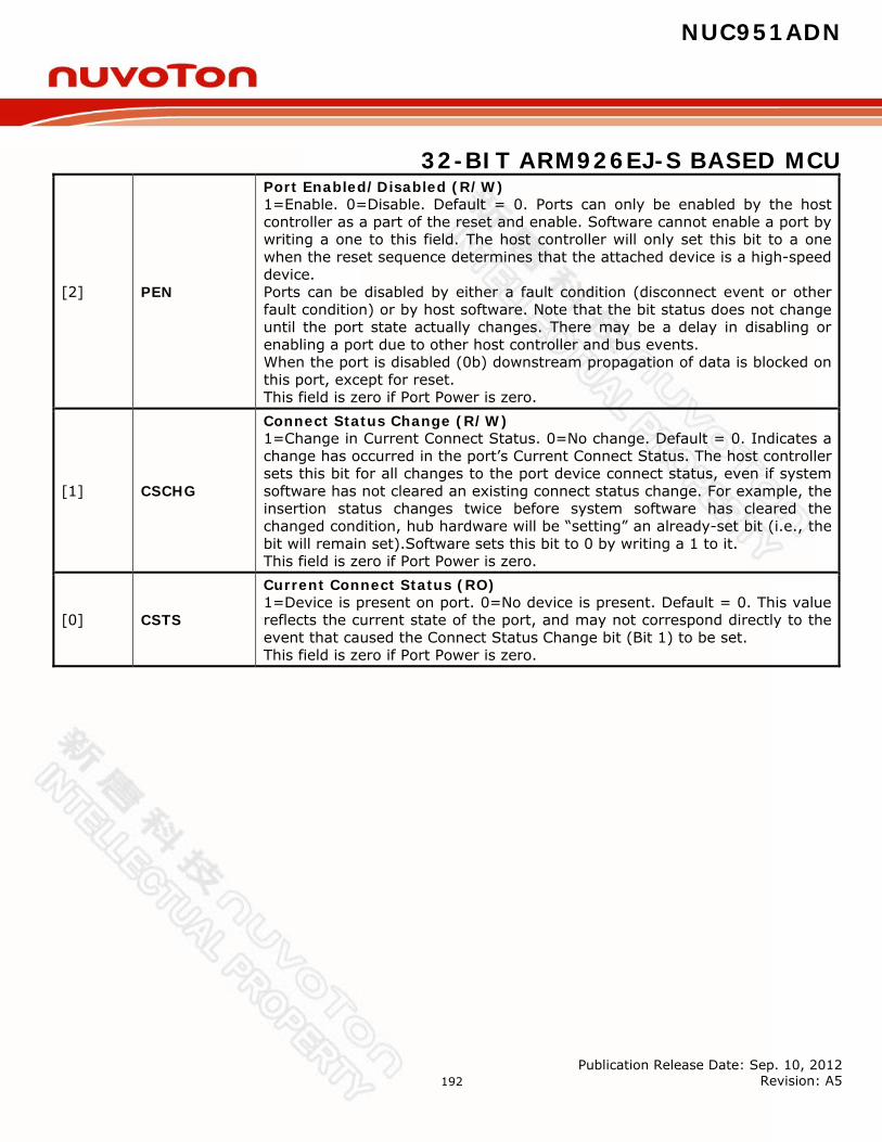
NUC951ADN
32-BIT ARM926EJ-S BASED MCU
Publication Release Date: Sep. 10, 2012 Revision: A5
192
[2] PEN
Port Enabled/Disabled (R/W) 1=Enable. 0=Disable. Default = 0. Ports can only be enabled by the host controller as a part of the reset and enable. Software cannot enable a port by writing a one to this field. The host controller will only set this bit to a one when the reset sequence determines that the attached device is a high-speed device. Ports can be disabled by either a fault condition (disconnect event or other fault condition) or by host software. Note that the bit status does not change until the port state actually changes. There may be a delay in disabling or enabling a port due to other host controller and bus events. When the port is disabled (0b) downstream propagation of data is blocked on this port, except for reset. This field is zero if Port Power is zero.
[1] CSCHG
Connect Status Change (R/W) 1=Change in Current Connect Status. 0=No change. Default = 0. Indicates a change has occurred in the port’s Current Connect Status. The host controller sets this bit for all changes to the port device connect status, even if system software has not cleared an existing connect status change. For example, the insertion status changes twice before system software has cleared the changed condition, hub hardware will be “setting” an already-set bit (i.e., the bit will remain set).Software sets this bit to 0 by writing a 1 to it. This field is zero if Port Power is zero.
[0] CSTS
Current Connect Status (RO) 1=Device is present on port. 0=No device is present. Default = 0. This value reflects the current state of the port, and may not correspond directly to the event that caused the Connect Status Change bit (Bit 1) to be set. This field is zero if Port Power is zero.
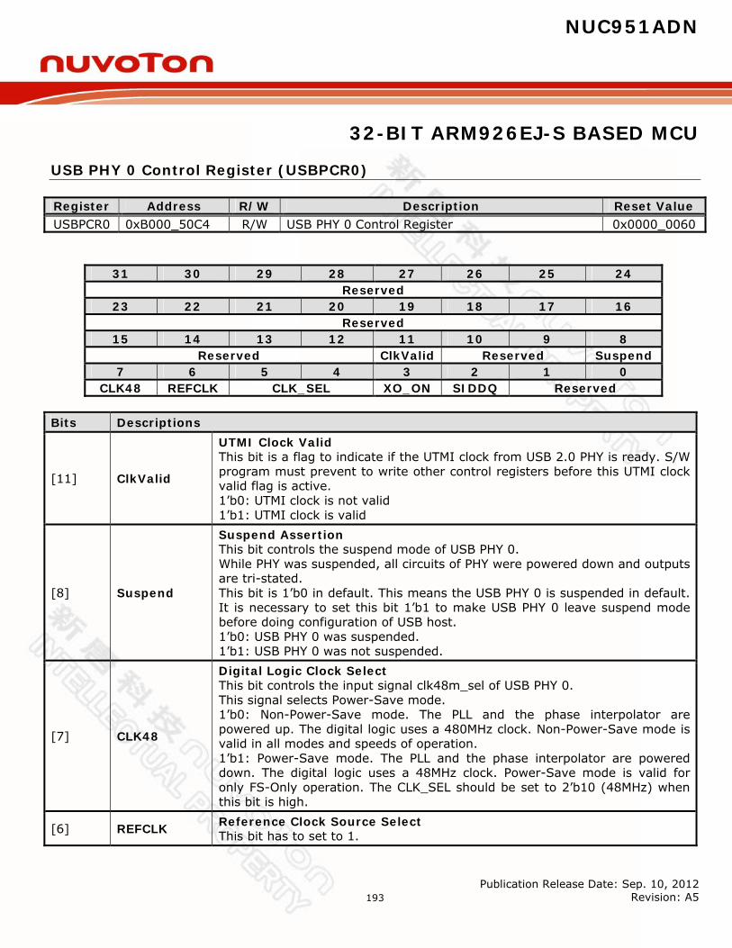
NUC951ADN
32-BIT ARM926EJ-S BASED MCU
Publication Release Date: Sep. 10, 2012 Revision: A5
193
USB PHY 0 Control Register (USBPCR0)
Register Address R/W Description Reset Value USBPCR0 0xB000_50C4 R/W USB PHY 0 Control Register 0x0000_0060
31 30 29 28 27 26 25 24 Reserved
23 22 21 20 19 18 17 16 Reserved
15 14 13 12 11 10 9 8 Reserved ClkValid Reserved Suspend
7 6 5 4 3 2 1 0 CLK48 REFCLK CLK_SEL XO_ON SIDDQ Reserved
Bits Descriptions
[11] ClkValid
UTMI Clock Valid This bit is a flag to indicate if the UTMI clock from USB 2.0 PHY is ready. S/W program must prevent to write other control registers before this UTMI clock valid flag is active. 1’b0: UTMI clock is not valid 1’b1: UTMI clock is valid
[8] Suspend
Suspend Assertion This bit controls the suspend mode of USB PHY 0. While PHY was suspended, all circuits of PHY were powered down and outputs are tri-stated. This bit is 1’b0 in default. This means the USB PHY 0 is suspended in default. It is necessary to set this bit 1’b1 to make USB PHY 0 leave suspend mode before doing configuration of USB host. 1’b0: USB PHY 0 was suspended. 1’b1: USB PHY 0 was not suspended.
[7] CLK48
Digital Logic Clock Select This bit controls the input signal clk48m_sel of USB PHY 0. This signal selects Power-Save mode. 1’b0: Non-Power-Save mode. The PLL and the phase interpolator are powered up. The digital logic uses a 480MHz clock. Non-Power-Save mode is valid in all modes and speeds of operation. 1’b1: Power-Save mode. The PLL and the phase interpolator are powered down. The digital logic uses a 48MHz clock. Power-Save mode is valid for only FS-Only operation. The CLK_SEL should be set to 2’b10 (48MHz) when this bit is high.
[6] REFCLK Reference Clock Source Select This bit has to set to 1.
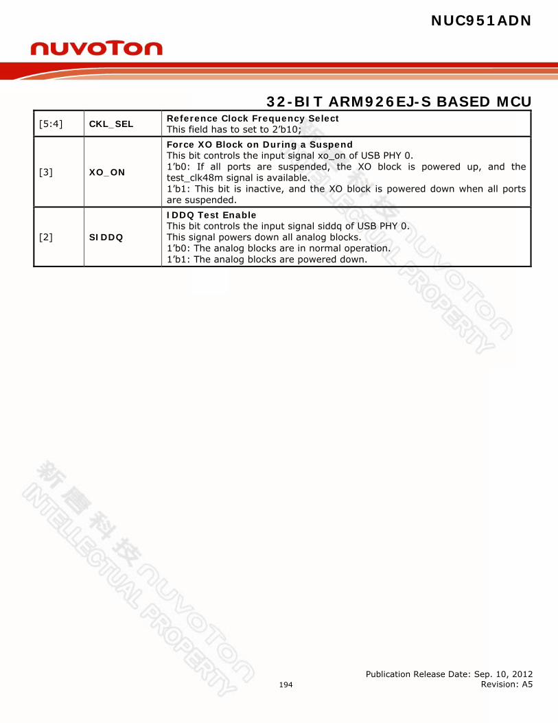
NUC951ADN
32-BIT ARM926EJ-S BASED MCU
Publication Release Date: Sep. 10, 2012 Revision: A5
194
[5:4] CKL_SEL Reference Clock Frequency Select This field has to set to 2’b10;
[3] XO_ON
Force XO Block on During a Suspend This bit controls the input signal xo_on of USB PHY 0. 1’b0: If all ports are suspended, the XO block is powered up, and the test_clk48m signal is available. 1’b1: This bit is inactive, and the XO block is powered down when all ports are suspended.
[2] SIDDQ
IDDQ Test Enable This bit controls the input signal siddq of USB PHY 0. This signal powers down all analog blocks. 1’b0: The analog blocks are in normal operation. 1’b1: The analog blocks are powered down.

NUC951ADN
32-BIT ARM926EJ-S BASED MCU
Publication Release Date: Sep. 10, 2012 Revision: A5
195
USB PHY 1 Control Register (USBPCR1)
Register Address R/W Description Reset Value USBPCR1 0xB000_50C8 R/W USB PHY 1 Control Register 0x0000_0020
31 30 29 28 27 26 25 24 Reserved
23 22 21 20 19 18 17 16 Reserved
15 14 13 12 11 10 9 8 Reserved XO_SEL Reserved Suspend
7 6 5 4 3 2 1 0 CLK48 REFCLK CLK_SEL XO_ON SIDDQ Reserved
Bits Descriptions
[11] XO_SEL
Clock Select for XO Block This bit defines the clock source of PHY1’s XO block is from external clock or a crystal. 1’b0: The XO block uses a 48MHz external clock supplied from PHY 0 1’b1: The XO block uses the clock from a crystal
[8] Suspend
Suspend Assertion This bit controls the suspend mode of USB PHY 1. While PHY was suspended, all circuits of PHY were powered down and outputs are tri-stated. This bit is 1’b0 in default. This means the USB PHY 1 is suspended in default. It is necessary to set this bit 1’b1 to make USB PHY 1 leave suspend mode before doing configuration of USB host. 1’b0: USB PHY 1 was suspended. 1’b1: USB PHY 1 was not suspended.
[7] CLK48
Digital Logic Clock Select This bit controls the input signal clk48m_sel of USB PHY 1. This signal selects Power-Save mode. 1’b0: Non-Power-Save mode. The PLL and the phase interpolator are powered up. The digital logic uses a 480MHz clock. Non-Power-Save mode is valid in all modes and speeds of operation. 1’b1: Power-Save mode. The PLL and the phase interpolator are powered down. The digital logic uses a 48MHz clock. Power-Save mode is valid for only FS-Only operation. The CLK_SEL should be set to 2’b10 (48MHz) when this bit is high.
[6] REFCLK Reference Clock Source Select This bit has to set to 0.
[5:4] CKL_SEL Reference Clock Frequency Select This field has to set to 2’b10.
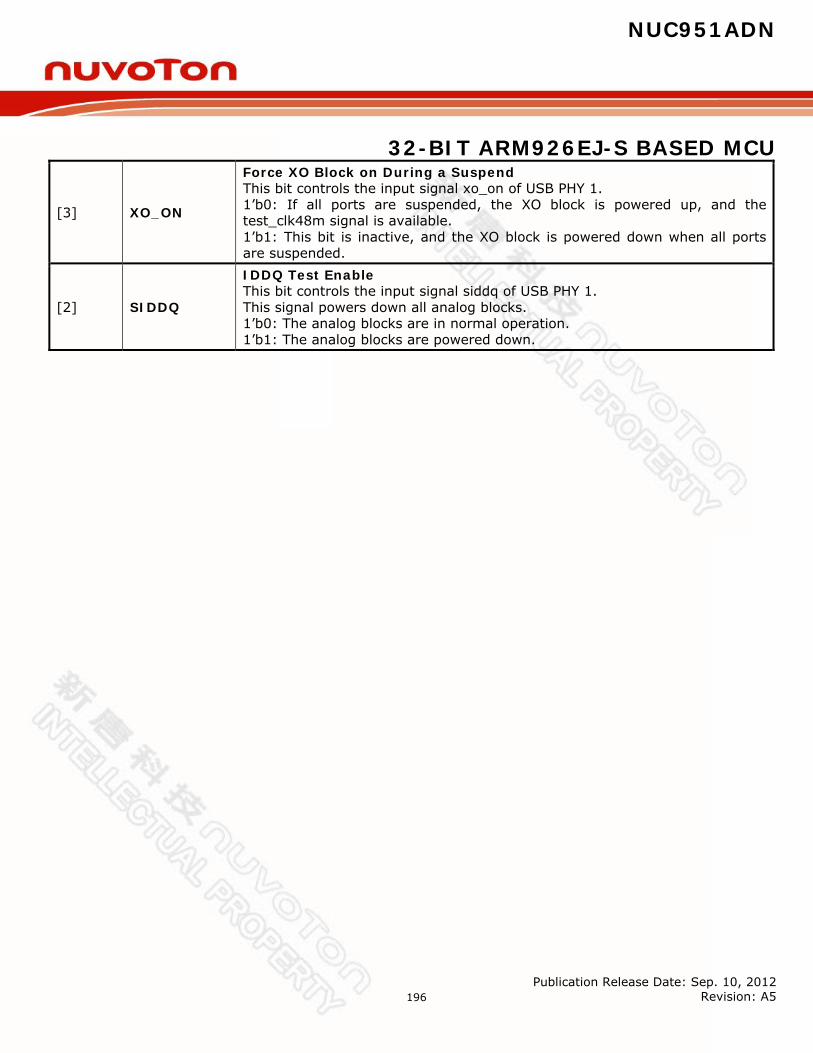
NUC951ADN
32-BIT ARM926EJ-S BASED MCU
Publication Release Date: Sep. 10, 2012 Revision: A5
196
[3] XO_ON
Force XO Block on During a Suspend This bit controls the input signal xo_on of USB PHY 1. 1’b0: If all ports are suspended, the XO block is powered up, and the test_clk48m signal is available. 1’b1: This bit is inactive, and the XO block is powered down when all ports are suspended.
[2] SIDDQ
IDDQ Test Enable This bit controls the input signal siddq of USB PHY 1. This signal powers down all analog blocks. 1’b0: The analog blocks are in normal operation. 1’b1: The analog blocks are powered down.
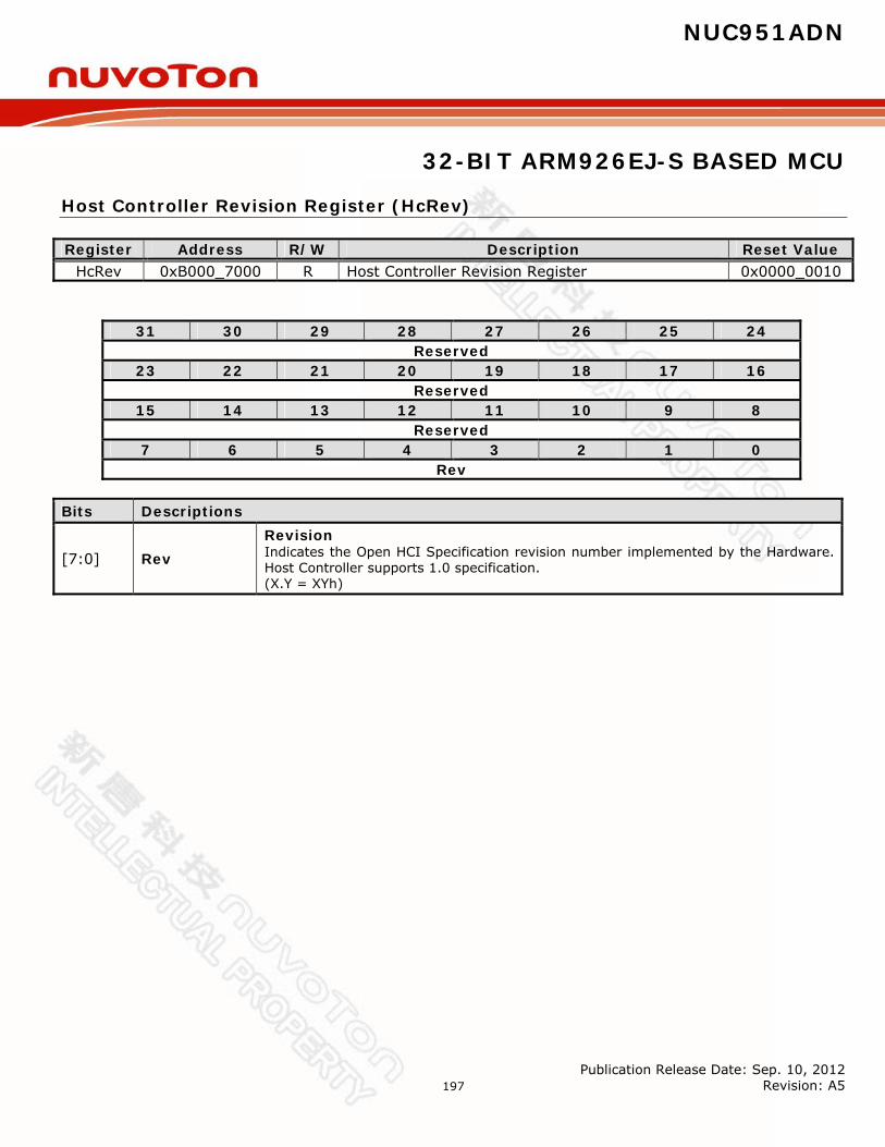
NUC951ADN
32-BIT ARM926EJ-S BASED MCU
Publication Release Date: Sep. 10, 2012 Revision: A5
197
Host Controller Revision Register (HcRev)
Register Address R/W Description Reset Value HcRev 0xB000_7000 R Host Controller Revision Register 0x0000_0010
31 30 29 28 27 26 25 24 Reserved
23 22 21 20 19 18 17 16 Reserved
15 14 13 12 11 10 9 8 Reserved
7 6 5 4 3 2 1 0 Rev
Bits Descriptions
[7:0] Rev Revision Indicates the Open HCI Specification revision number implemented by the Hardware. Host Controller supports 1.0 specification. (X.Y = XYh)
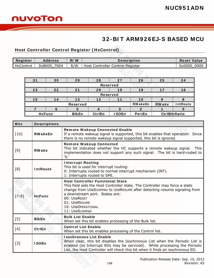
NUC951ADN
32-BIT ARM926EJ-S BASED MCU
Publication Release Date: Sep. 10, 2012 Revision: A5
198
Host Controller Control Register (HcControl)
Register Address R/W Description Reset Value HcControl 0xB000_7004 R/W Host Controller Control Register 0x0000_0000
31 30 29 28 27 26 25 24 Reserved
23 22 21 20 19 18 17 16 Reserved
15 14 13 12 11 10 9 8 Reserved RWakeEn RWake IntRoute
7 6 5 4 3 2 1 0 HcFunc BlkEn CtrlEn ISOEn PeriEn CtrlBlkRatio
Bits Descriptions
[10] RWakeEn Remote Wakeup Connected Enable If a remote wakeup signal is supported, this bit enables that operation. Since there is no remote wakeup signal supported, this bit is ignored.
[9] RWake
Remote Wakeup Connected This bit indicated whether the HC supports a remote wakeup signal. This implementation does not support any such signal. The bit is hard-coded to ‘0.’
[8] IntRoute
Interrupt Routing This bit is used for interrupt routing: 0: Interrupts routed to normal interrupt mechanism (INT). 1: Interrupts routed to SMI.
[7:6] HcFunc
Host Controller Functional State This field sets the Host Controller state. The Controller may force a state change from USBSUSPEND to USBRESUME after detecting resume signaling from a downstream port. States are: 00: USBRESET 01: USBRESUME 10: USBOPERATIONAL 11: USBSUSPEND
[5] BlkEn Bulk List Enable When set this bit enables processing of the Bulk list.
[4] CtrlEn Control List Enable When set this bit enables processing of the Control list.
[3] ISOEn
Isochronous List Enable When clear, this bit disables the Isochronous List when the Periodic List is enabled (so Interrupt EDs may be serviced). While processing the Periodic List, the Host Controller will check this bit when it finds an isochronous ED.
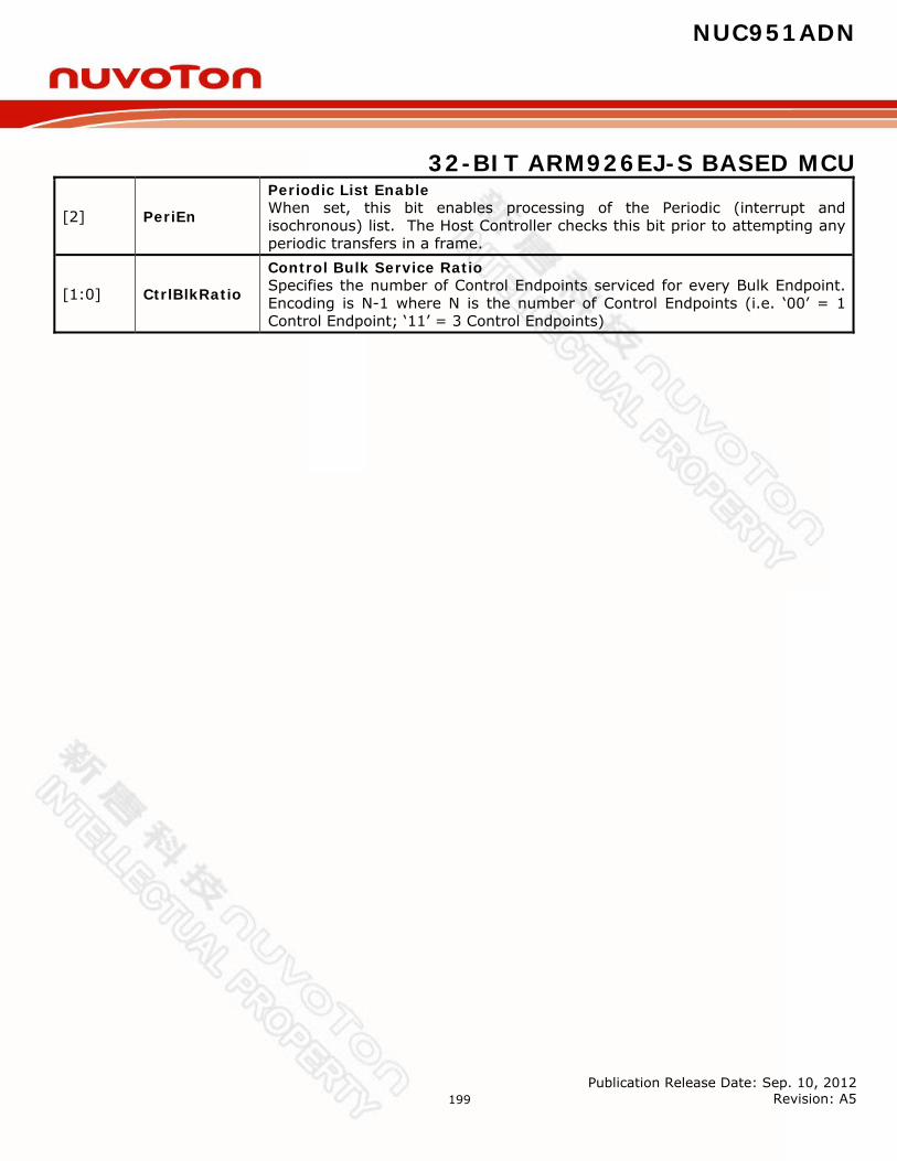
NUC951ADN
32-BIT ARM926EJ-S BASED MCU
Publication Release Date: Sep. 10, 2012 Revision: A5
199
[2] PeriEn
Periodic List Enable When set, this bit enables processing of the Periodic (interrupt and isochronous) list. The Host Controller checks this bit prior to attempting any periodic transfers in a frame.
[1:0] CtrlBlkRatio
Control Bulk Service Ratio Specifies the number of Control Endpoints serviced for every Bulk Endpoint. Encoding is N-1 where N is the number of Control Endpoints (i.e. ‘00’ = 1 Control Endpoint; ‘11’ = 3 Control Endpoints)

NUC951ADN
32-BIT ARM926EJ-S BASED MCU
Publication Release Date: Sep. 10, 2012 Revision: A5
200
Host Controller Command Status Register (HcComSts)
Register Address R/W Description Reset Value HcComSts 0xB000_7008 R/W Host Controller Command Status Register 0x0000_0000
31 30 29 28 27 26 25 24 Reserved
23 22 21 20 19 18 17 16 Reserved SchOverRun
15 14 13 12 11 10 9 8 Reserved
7 6 5 4 3 2 1 0 Reserved OCReq BlkFill CtrlFill HCReset
Bits Descriptions
[17:16] SchOverRun Schedule Overrun Count This field is increment every time the SchedulingOverrun bit in HcInterruptStatus is set. The count wraps from ‘11’ to ‘00.’
[3] OCReq Ownership Chang Request When set by software, this bit sets the OwnershipChange field in HcInterruptStatus. The bit is cleared by software.
[2] BlkFill
Bulk List Filled Set to indicate there is an active ED on the Bulk List. The bit may be set by either software or the Host Controller and cleared by the Host Controller each time it begins processing the head of the Bulk List.
[1] CtrlFill
Control List Filled Set to indicate there is an active ED on the Control List. It may be set by either software or the Host Controller and cleared by the Host Controller each time it begins processing the head of the Control List.
[0] HCReset Host Controller Reset This bit is set to initiate the software reset. This bit is cleared by the Host Controller, upon completed of the reset operation.
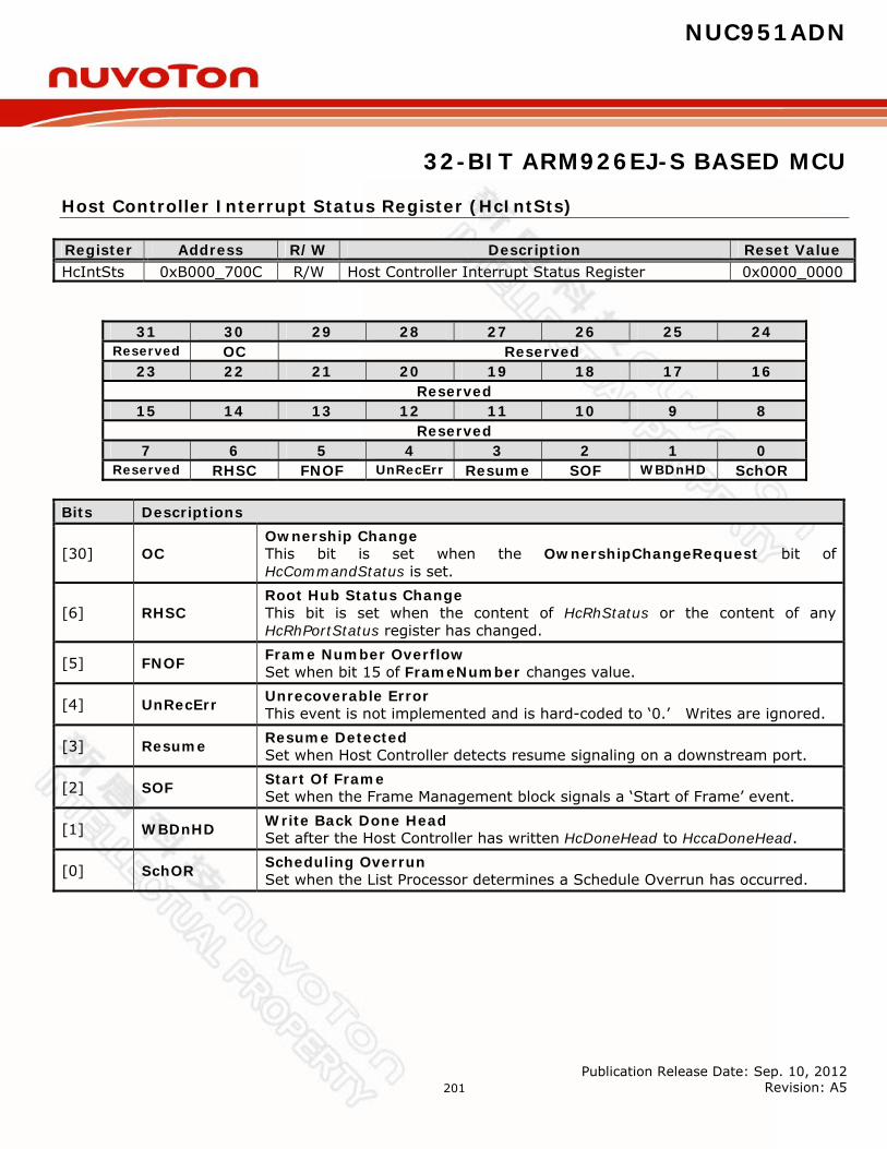
NUC951ADN
32-BIT ARM926EJ-S BASED MCU
Publication Release Date: Sep. 10, 2012 Revision: A5
201
Host Controller Interrupt Status Register (HcIntSts)
Register Address R/W Description Reset Value HcIntSts 0xB000_700C R/W Host Controller Interrupt Status Register 0x0000_0000
31 30 29 28 27 26 25 24 Reserved OC Reserved
23 22 21 20 19 18 17 16 Reserved
15 14 13 12 11 10 9 8 Reserved
7 6 5 4 3 2 1 0 Reserved RHSC FNOF UnRecErr Resume SOF WBDnHD SchOR
Bits Descriptions
[30] OC Ownership Change This bit is set when the OwnershipChangeRequest bit of HcCommandStatus is set.
[6] RHSC Root Hub Status Change This bit is set when the content of HcRhStatus or the content of any HcRhPortStatus register has changed.
[5] FNOF Frame Number Overflow Set when bit 15 of FrameNumber changes value.
[4] UnRecErr Unrecoverable Error This event is not implemented and is hard-coded to ‘0.’ Writes are ignored.
[3] Resume Resume Detected Set when Host Controller detects resume signaling on a downstream port.
[2] SOF Start Of Frame Set when the Frame Management block signals a ‘Start of Frame’ event.
[1] WBDnHD Write Back Done Head Set after the Host Controller has written HcDoneHead to HccaDoneHead.
[0] SchOR Scheduling Overrun Set when the List Processor determines a Schedule Overrun has occurred.
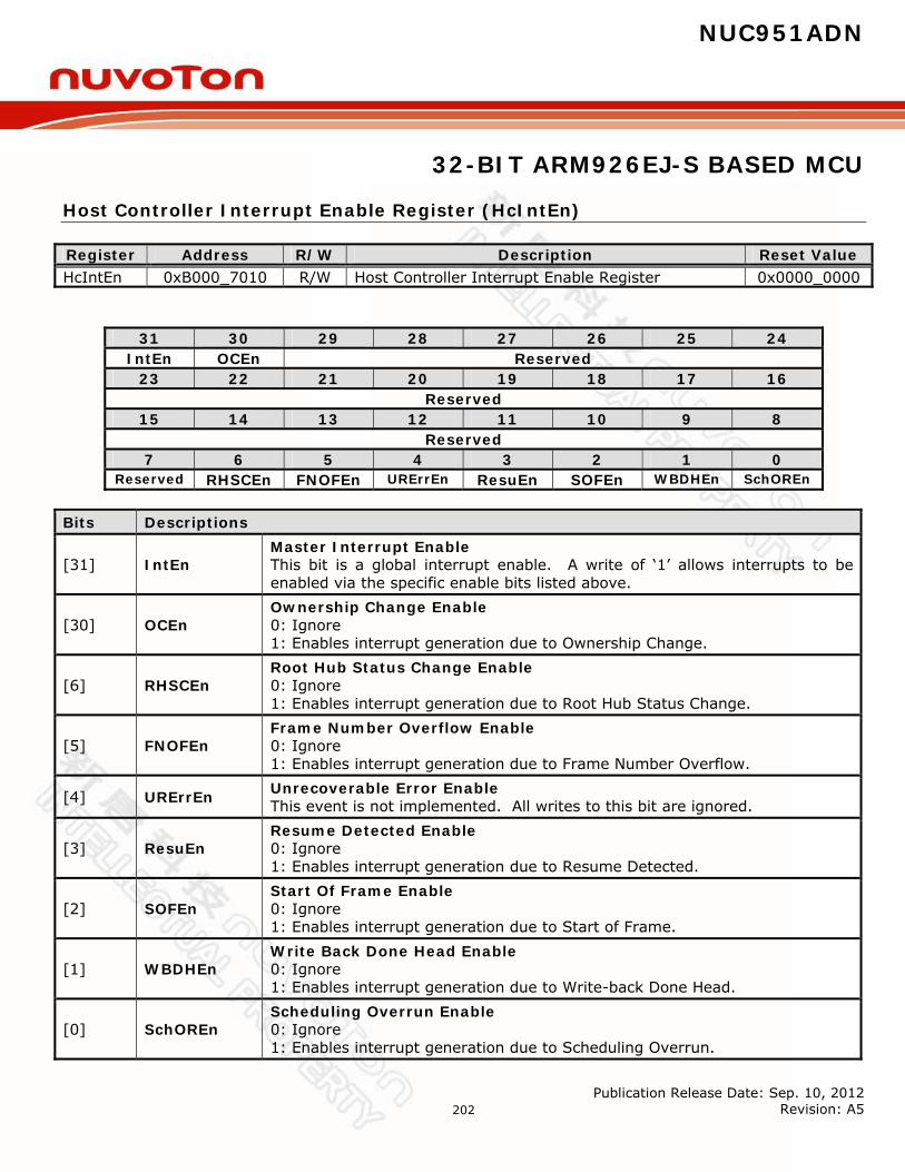
NUC951ADN
32-BIT ARM926EJ-S BASED MCU
Publication Release Date: Sep. 10, 2012 Revision: A5
202
Host Controller Interrupt Enable Register (HcIntEn)
Register Address R/W Description Reset Value HcIntEn 0xB000_7010 R/W Host Controller Interrupt Enable Register 0x0000_0000
31 30 29 28 27 26 25 24 IntEn OCEn Reserved
23 22 21 20 19 18 17 16 Reserved
15 14 13 12 11 10 9 8 Reserved
7 6 5 4 3 2 1 0 Reserved RHSCEn FNOFEn URErrEn ResuEn SOFEn WBDHEn SchOREn
Bits Descriptions
[31] IntEn Master Interrupt Enable This bit is a global interrupt enable. A write of ‘1’ allows interrupts to be enabled via the specific enable bits listed above.
[30] OCEn Ownership Change Enable 0: Ignore 1: Enables interrupt generation due to Ownership Change.
[6] RHSCEn Root Hub Status Change Enable 0: Ignore 1: Enables interrupt generation due to Root Hub Status Change.
[5] FNOFEn Frame Number Overflow Enable 0: Ignore 1: Enables interrupt generation due to Frame Number Overflow.
[4] URErrEn Unrecoverable Error Enable This event is not implemented. All writes to this bit are ignored.
[3] ResuEn Resume Detected Enable 0: Ignore 1: Enables interrupt generation due to Resume Detected.
[2] SOFEn Start Of Frame Enable 0: Ignore 1: Enables interrupt generation due to Start of Frame.
[1] WBDHEn Write Back Done Head Enable 0: Ignore 1: Enables interrupt generation due to Write-back Done Head.
[0] SchOREn Scheduling Overrun Enable 0: Ignore 1: Enables interrupt generation due to Scheduling Overrun.
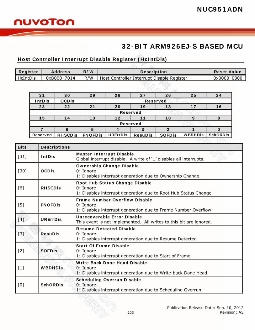
NUC951ADN
32-BIT ARM926EJ-S BASED MCU
Publication Release Date: Sep. 10, 2012 Revision: A5
203
Host Controller Interrupt Disable Register (HcIntDis)
Register Address R/W Description Reset Value HcIntDis 0xB000_7014 R/W Host Controller Interrupt Disable Register 0x0000_0000
31 30 29 28 27 26 25 24 IntDis OCDis Reserved
23 22 21 20 19 18 17 16 Reserved
15 14 13 12 11 10 9 8 Reserved
7 6 5 4 3 2 1 0 Reserved RHSCDis FNOFDis URErrDis ResuDis SOFDis WBDHDis SchORDis
Bits Descriptions
[31] IntDis Master Interrupt Disable Global interrupt disable. A write of ‘1’ disables all interrupts.
[30] OCDis Ownership Change Disable 0: Ignore 1: Disables interrupt generation due to Ownership Change.
[6] RHSCDis Root Hub Status Change Disable 0: Ignore 1: Disables interrupt generation due to Root Hub Status Change.
[5] FNOFDis Frame Number Overflow Disable 0: Ignore 1: Disables interrupt generation due to Frame Number Overflow.
[4] URErrDis Unrecoverable Error Disable This event is not implemented. All writes to this bit are ignored.
[3] ResuDis Resume Detected Disable 0: Ignore 1: Disables interrupt generation due to Resume Detected.
[2] SOFDis Start Of Frame Disable 0: Ignore 1: Disables interrupt generation due to Start of Frame.
[1] WBDHDis Write Back Done Head Disable 0: Ignore 1: Disables interrupt generation due to Write-back Done Head.
[0] SchORDis Scheduling Overrun Disable 0: Ignore 1: Disables interrupt generation due to Scheduling Overrun.

NUC951ADN
32-BIT ARM926EJ-S BASED MCU
Publication Release Date: Sep. 10, 2012 Revision: A5
204
Host Controller Communication Area Register (HcHCCA)
Register Address R/W Description Reset Value HcHCCA 0xB000_7018 R/W Host Controller Communication Area Register 0x0000_0000
31 30 29 28 27 26 25 24 HCCA
23 22 21 20 19 18 17 16 HCCA
15 14 13 12 11 10 9 8 HCCA
7 6 5 4 3 2 1 0 Reserved
Bits Descriptions
[31:7] HCCA Host Controller Communication Area Pointer to HCCA base address.
Host Controller Period Current ED Register (HcPerCED)
Register Address R/W Description Reset Value HcPerCED 0xB000_701C R/W Host Controller Period Current ED Register 0x0000_0000
31 30 29 28 27 26 25 24 PeriCED
23 22 21 20 19 18 17 16 PeriCED
15 14 13 12 11 10 9 8 PeriCED
7 6 5 4 3 2 1 0 PeriCED Reserved
Bits Descriptions
[31:4] PeriCED Periodic Current ED Pointer to the current Periodic List ED.
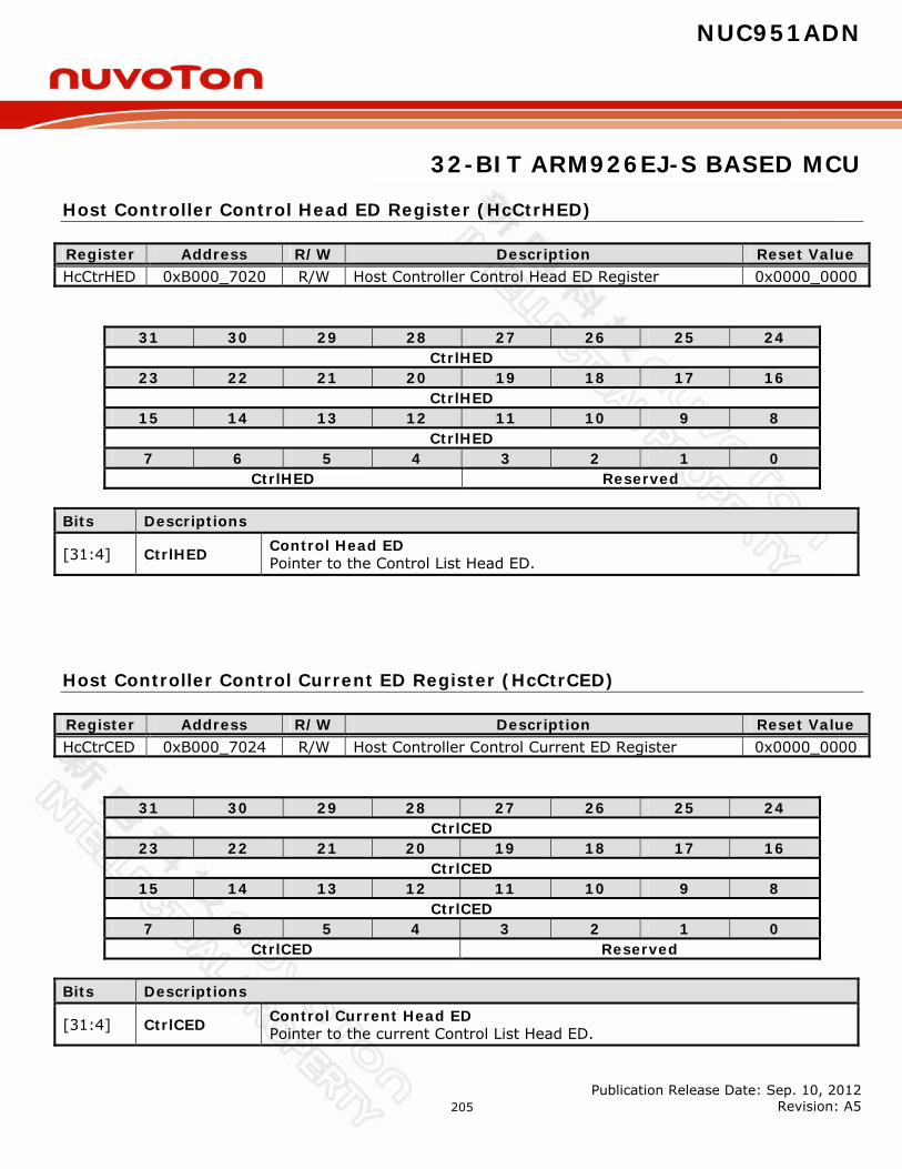
NUC951ADN
32-BIT ARM926EJ-S BASED MCU
Publication Release Date: Sep. 10, 2012 Revision: A5
205
Host Controller Control Head ED Register (HcCtrHED)
Register Address R/W Description Reset Value HcCtrHED 0xB000_7020 R/W Host Controller Control Head ED Register 0x0000_0000
31 30 29 28 27 26 25 24 CtrlHED
23 22 21 20 19 18 17 16 CtrlHED
15 14 13 12 11 10 9 8 CtrlHED
7 6 5 4 3 2 1 0 CtrlHED Reserved
Bits Descriptions
[31:4] CtrlHED Control Head ED Pointer to the Control List Head ED.
Host Controller Control Current ED Register (HcCtrCED)
Register Address R/W Description Reset Value HcCtrCED 0xB000_7024 R/W Host Controller Control Current ED Register 0x0000_0000
31 30 29 28 27 26 25 24 CtrlCED
23 22 21 20 19 18 17 16 CtrlCED
15 14 13 12 11 10 9 8 CtrlCED
7 6 5 4 3 2 1 0 CtrlCED Reserved
Bits Descriptions
[31:4] CtrlCED Control Current Head ED Pointer to the current Control List Head ED.
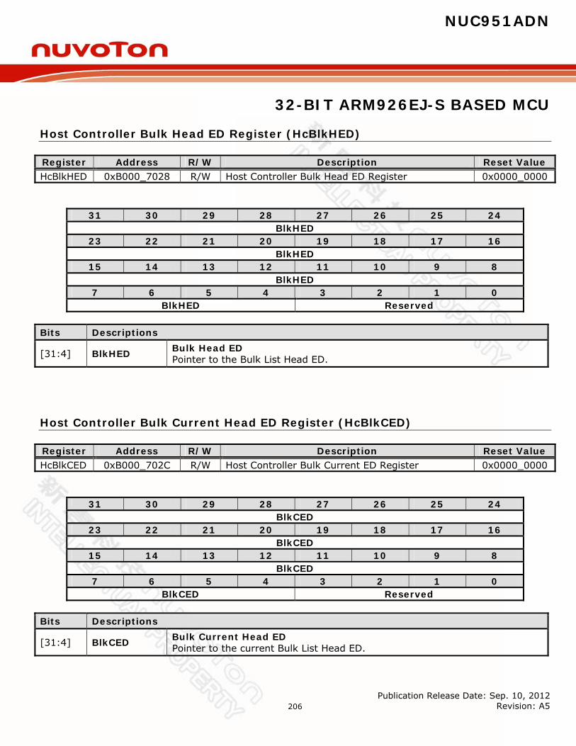
NUC951ADN
32-BIT ARM926EJ-S BASED MCU
Publication Release Date: Sep. 10, 2012 Revision: A5
206
Host Controller Bulk Head ED Register (HcBlkHED)
Register Address R/W Description Reset Value HcBlkHED 0xB000_7028 R/W Host Controller Bulk Head ED Register 0x0000_0000
31 30 29 28 27 26 25 24 BlkHED
23 22 21 20 19 18 17 16 BlkHED
15 14 13 12 11 10 9 8 BlkHED
7 6 5 4 3 2 1 0 BlkHED Reserved
Bits Descriptions
[31:4] BlkHED Bulk Head ED Pointer to the Bulk List Head ED.
Host Controller Bulk Current Head ED Register (HcBlkCED)
Register Address R/W Description Reset Value HcBlkCED 0xB000_702C R/W Host Controller Bulk Current ED Register 0x0000_0000
31 30 29 28 27 26 25 24 BlkCED
23 22 21 20 19 18 17 16 BlkCED
15 14 13 12 11 10 9 8 BlkCED
7 6 5 4 3 2 1 0 BlkCED Reserved
Bits Descriptions
[31:4] BlkCED Bulk Current Head ED Pointer to the current Bulk List Head ED.

NUC951ADN
32-BIT ARM926EJ-S BASED MCU
Publication Release Date: Sep. 10, 2012 Revision: A5
207
Host Controller Done Head Register (HcDoneH)
Register Address R/W Description Reset Value HcDoneH 0xB000_7030 R/W Host Controller Done Head Register 0x0000_0000
31 30 29 28 27 26 25 24 DoneH
23 22 21 20 19 18 17 16 DoneH
15 14 13 12 11 10 9 8 DoneH
7 6 5 4 3 2 1 0 DoneH Reserved
Bits Descriptions
[31:4] DoneH Done Head Pointer to the current Done List Head ED.

NUC951ADN
32-BIT ARM926EJ-S BASED MCU
Publication Release Date: Sep. 10, 2012 Revision: A5
208
Host Controller Frame Interval Register (HcFmIntv)
Register Address R/W Description Reset Value HcFmIntv 0xB000_7034 R/W Host Controller Frame Interval Register 0x0000_2EDF
31 30 29 28 27 26 25 24 FmIntvT FSDPktCnt
23 22 21 20 19 18 17 16 FSDPktCnt
15 14 13 12 11 10 9 8 Reserved FmInterval
7 6 5 4 3 2 1 0 FmInterval
Bits Descriptions
[31] FmIntvT Frame Interval Toggle This bit is toggled by HCD when it loads a new value into FrameInterval.
[30: 16] FSDPktCnt FS Largest Data Packet This field specifies a value that is loaded into the Largest Data Packet Counter at the beginning of each frame.
[13:0] FmInterval Frame Interval This field specifies the length of a frame as (bit times - 1). For 12,000 bit times in a frame, a value of 11,999 is stored here.
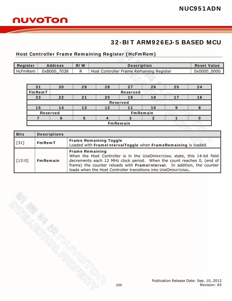
NUC951ADN
32-BIT ARM926EJ-S BASED MCU
Publication Release Date: Sep. 10, 2012 Revision: A5
209
Host Controller Frame Remaining Register (HcFmRem)
Register Address R/W Description Reset Value HcFmRem 0xB000_7038 R Host Controller Frame Remaining Register 0x0000_0000
31 30 29 28 27 26 25 24 FmRemT Reserved
23 22 21 20 19 18 17 16 Reserved
15 14 13 12 11 10 9 8 Reserved FmRemain
7 6 5 4 3 2 1 0 FmRemain
Bits Descriptions
[31] FmRemT Frame Remaining Toggle Loaded with FrameIntervalToggle when FrameRemaining is loaded.
[13:0] FmRemain
Frame Remaining When the Host Controller is in the USBOPERATIONAL state, this 14-bit field decrements each 12 MHz clock period. When the count reaches 0, (end of frame) the counter reloads with FrameInterval. In addition, the counter loads when the Host Controller transitions into USBOPERATIONAL.
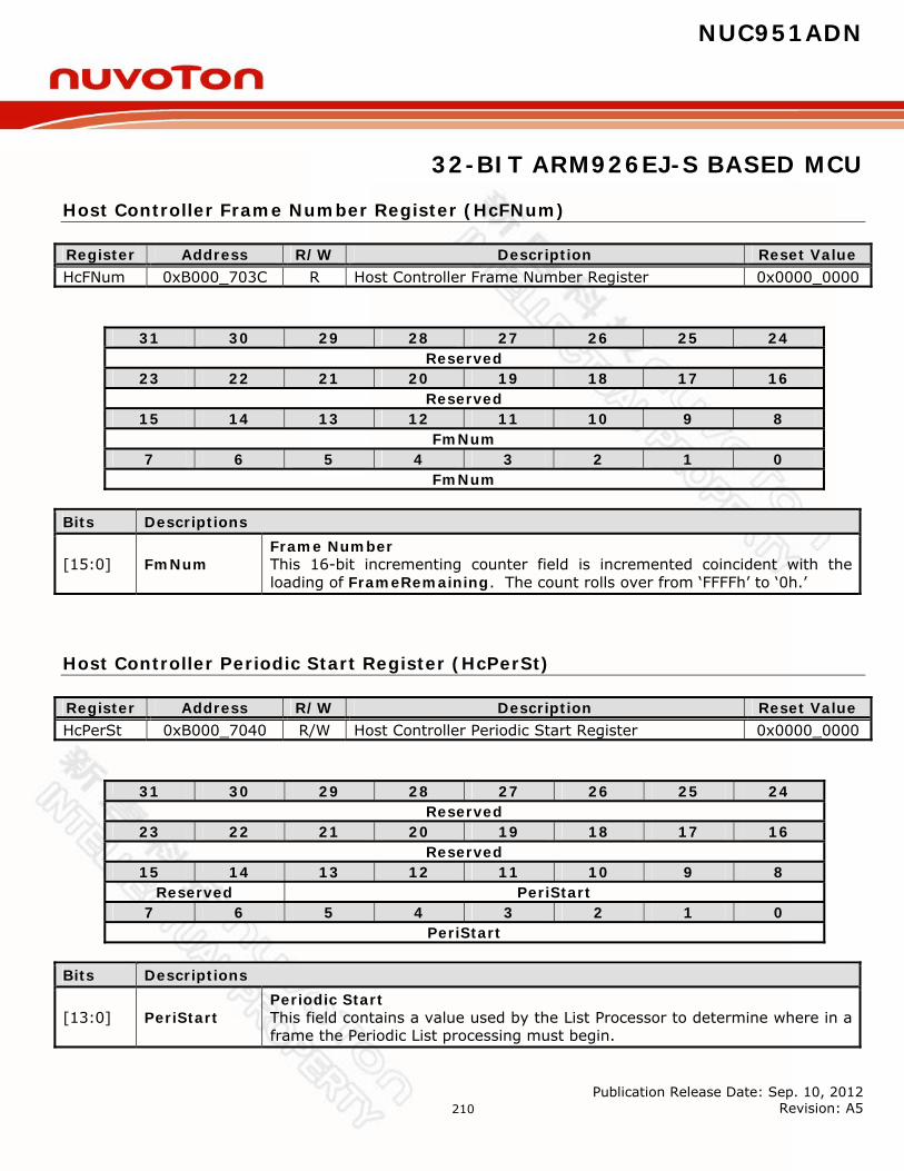
NUC951ADN
32-BIT ARM926EJ-S BASED MCU
Publication Release Date: Sep. 10, 2012 Revision: A5
210
Host Controller Frame Number Register (HcFNum)
Register Address R/W Description Reset Value HcFNum 0xB000_703C R Host Controller Frame Number Register 0x0000_0000
31 30 29 28 27 26 25 24 Reserved
23 22 21 20 19 18 17 16 Reserved
15 14 13 12 11 10 9 8 FmNum
7 6 5 4 3 2 1 0 FmNum
Bits Descriptions
[15:0] FmNum Frame Number This 16-bit incrementing counter field is incremented coincident with the loading of FrameRemaining. The count rolls over from ‘FFFFh’ to ‘0h.’
Host Controller Periodic Start Register (HcPerSt)
Register Address R/W Description Reset Value HcPerSt 0xB000_7040 R/W Host Controller Periodic Start Register 0x0000_0000
31 30 29 28 27 26 25 24 Reserved
23 22 21 20 19 18 17 16 Reserved
15 14 13 12 11 10 9 8 Reserved PeriStart
7 6 5 4 3 2 1 0 PeriStart
Bits Descriptions
[13:0] PeriStart Periodic Start This field contains a value used by the List Processor to determine where in a frame the Periodic List processing must begin.
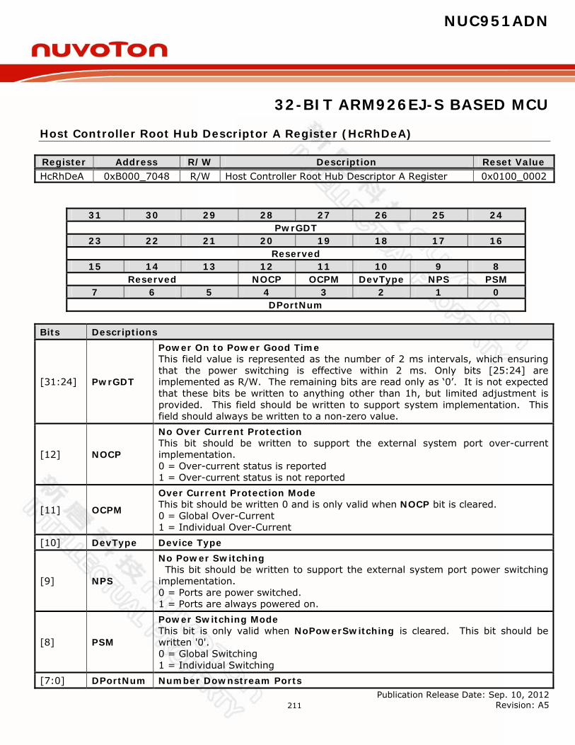
NUC951ADN
32-BIT ARM926EJ-S BASED MCU
Publication Release Date: Sep. 10, 2012 Revision: A5
211
Host Controller Root Hub Descriptor A Register (HcRhDeA)
Register Address R/W Description Reset Value HcRhDeA 0xB000_7048 R/W Host Controller Root Hub Descriptor A Register 0x0100_0002
31 30 29 28 27 26 25 24 PwrGDT
23 22 21 20 19 18 17 16 Reserved
15 14 13 12 11 10 9 8 Reserved NOCP OCPM DevType NPS PSM
7 6 5 4 3 2 1 0 DPortNum
Bits Descriptions
[31:24] PwrGDT
Power On to Power Good Time This field value is represented as the number of 2 ms intervals, which ensuring that the power switching is effective within 2 ms. Only bits [25:24] are implemented as R/W. The remaining bits are read only as ‘0’. It is not expected that these bits be written to anything other than 1h, but limited adjustment is provided. This field should be written to support system implementation. This field should always be written to a non-zero value.
[12] NOCP
No Over Current Protection This bit should be written to support the external system port over-current implementation. 0 = Over-current status is reported 1 = Over-current status is not reported
[11] OCPM
Over Current Protection Mode This bit should be written 0 and is only valid when NOCP bit is cleared. 0 = Global Over-Current 1 = Individual Over-Current
[10] DevType Device Type
[9] NPS
No Power Switching This bit should be written to support the external system port power switching implementation. 0 = Ports are power switched. 1 = Ports are always powered on.
[8] PSM
Power Switching Mode This bit is only valid when NoPowerSwitching is cleared. This bit should be written '0'. 0 = Global Switching 1 = Individual Switching
[7:0] DPortNum Number Downstream Ports
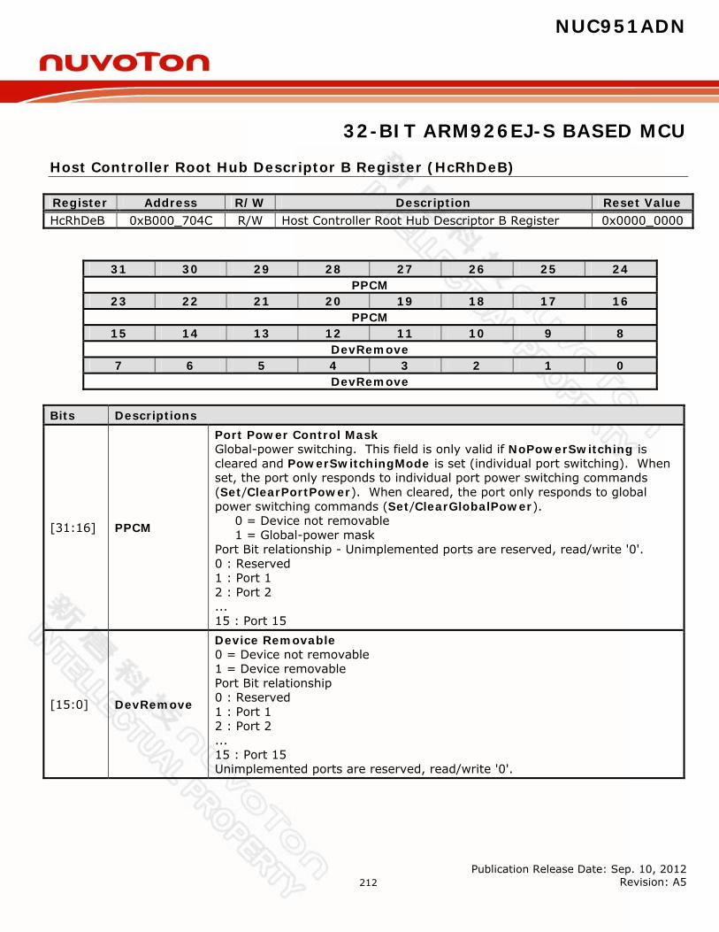
NUC951ADN
32-BIT ARM926EJ-S BASED MCU
Publication Release Date: Sep. 10, 2012 Revision: A5
212
Host Controller Root Hub Descriptor B Register (HcRhDeB)
Register Address R/W Description Reset Value HcRhDeB 0xB000_704C R/W Host Controller Root Hub Descriptor B Register 0x0000_0000
31 30 29 28 27 26 25 24 PPCM
23 22 21 20 19 18 17 16 PPCM
15 14 13 12 11 10 9 8 DevRemove
7 6 5 4 3 2 1 0 DevRemove
Bits Descriptions
[31:16] PPCM
Port Power Control Mask Global-power switching. This field is only valid if NoPowerSwitching is cleared and PowerSwitchingMode is set (individual port switching). When set, the port only responds to individual port power switching commands (Set/ClearPortPower). When cleared, the port only responds to global power switching commands (Set/ClearGlobalPower). 0 = Device not removable 1 = Global-power mask Port Bit relationship - Unimplemented ports are reserved, read/write '0'. 0 : Reserved 1 : Port 1 2 : Port 2 ... 15 : Port 15
[15:0] DevRemove
Device Removable 0 = Device not removable 1 = Device removable Port Bit relationship 0 : Reserved 1 : Port 1 2 : Port 2 ... 15 : Port 15 Unimplemented ports are reserved, read/write '0'.

NUC951ADN
32-BIT ARM926EJ-S BASED MCU
Publication Release Date: Sep. 10, 2012 Revision: A5
213
Host Controller Root Hub Status Register (HcRhSts)
Register Address R/W Description Reset Value HcRhSts 0xB000_7050 R/W Host Controller Root Hub Status Register 0x0000_0000
31 30 29 28 27 26 25 24 RWEClr Reserved
23 22 21 20 19 18 17 16 Reserved OCIC LPSC
15 14 13 12 11 10 9 8 DRWEn Reserved
7 6 5 4 3 2 1 0 Reserved OC LPS
Bits Descriptions
[31] RWEClr Clear Remote Wakeup Enable Writing a '1' to this bit clears DeviceRemoteWakeupEnable. Writing a '1' has no effect.
[17] OCIC Over Current Indicator Change This bit is set when OverCurrentIndicator changes. Writing a '1' clears this bit. Writing a '0' has no effect.
[16] LPSC
(Read) LocalPowerStatusChange Not supported. Always read '0'. (Write) SetGlobalPower Write a '1' issues a SetGlobalPower command to the ports. Writing a '0' has no effect.
[15] DRWEn
(Read) DeviceRemoteWakeupEnable This bit enables ports' ConnectStatusChange as a remote wakeup event. 0 = disabled 1 = enabled (Write) SetRemoteWakeupEnable Writing a '1' sets DeviceRemoteWakeupEnable. Writing a '0' has no effect.
[1] OC
Over Current Indicator This bit reflects the state of the OVRCUR pin. This field is only valid if NoOverCurrentProtection and OverCurrentProtectionMode are cleared. 0 = No over-current condition 1 = Over-current condition
[0] LPS
(Read) LocalPowerStatus Not Supported. Always read '0'. (Write) ClearGlobalPower Writing a '1' issues a ClearGlobalPower command to the ports. Writing a '0' has no effect.
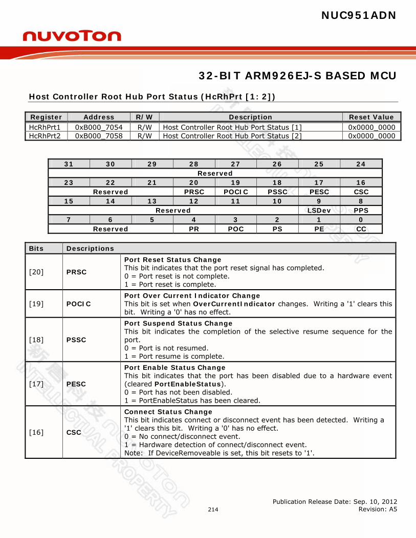
NUC951ADN
32-BIT ARM926EJ-S BASED MCU
Publication Release Date: Sep. 10, 2012 Revision: A5
214
Host Controller Root Hub Port Status (HcRhPrt [1: 2])
Register Address R/W Description Reset Value HcRhPrt1 0xB000_7054 R/W Host Controller Root Hub Port Status [1] 0x0000_0000 HcRhPrt2 0xB000_7058 R/W Host Controller Root Hub Port Status [2] 0x0000_0000
31 30 29 28 27 26 25 24 Reserved
23 22 21 20 19 18 17 16 Reserved PRSC POCIC PSSC PESC CSC
15 14 13 12 11 10 9 8 Reserved LSDev PPS
7 6 5 4 3 2 1 0 Reserved PR POC PS PE CC
Bits Descriptions
[20] PRSC
Port Reset Status Change This bit indicates that the port reset signal has completed. 0 = Port reset is not complete. 1 = Port reset is complete.
[19] POCIC Port Over Current Indicator Change This bit is set when OverCurrentIndicator changes. Writing a '1' clears this bit. Writing a '0' has no effect.
[18] PSSC
Port Suspend Status Change This bit indicates the completion of the selective resume sequence for the port. 0 = Port is not resumed. 1 = Port resume is complete.
[17] PESC
Port Enable Status Change This bit indicates that the port has been disabled due to a hardware event (cleared PortEnableStatus). 0 = Port has not been disabled. 1 = PortEnableStatus has been cleared.
[16] CSC
Connect Status Change This bit indicates connect or disconnect event has been detected. Writing a '1' clears this bit. Writing a '0' has no effect. 0 = No connect/disconnect event. 1 = Hardware detection of connect/disconnect event. Note: If DeviceRemoveable is set, this bit resets to '1'.
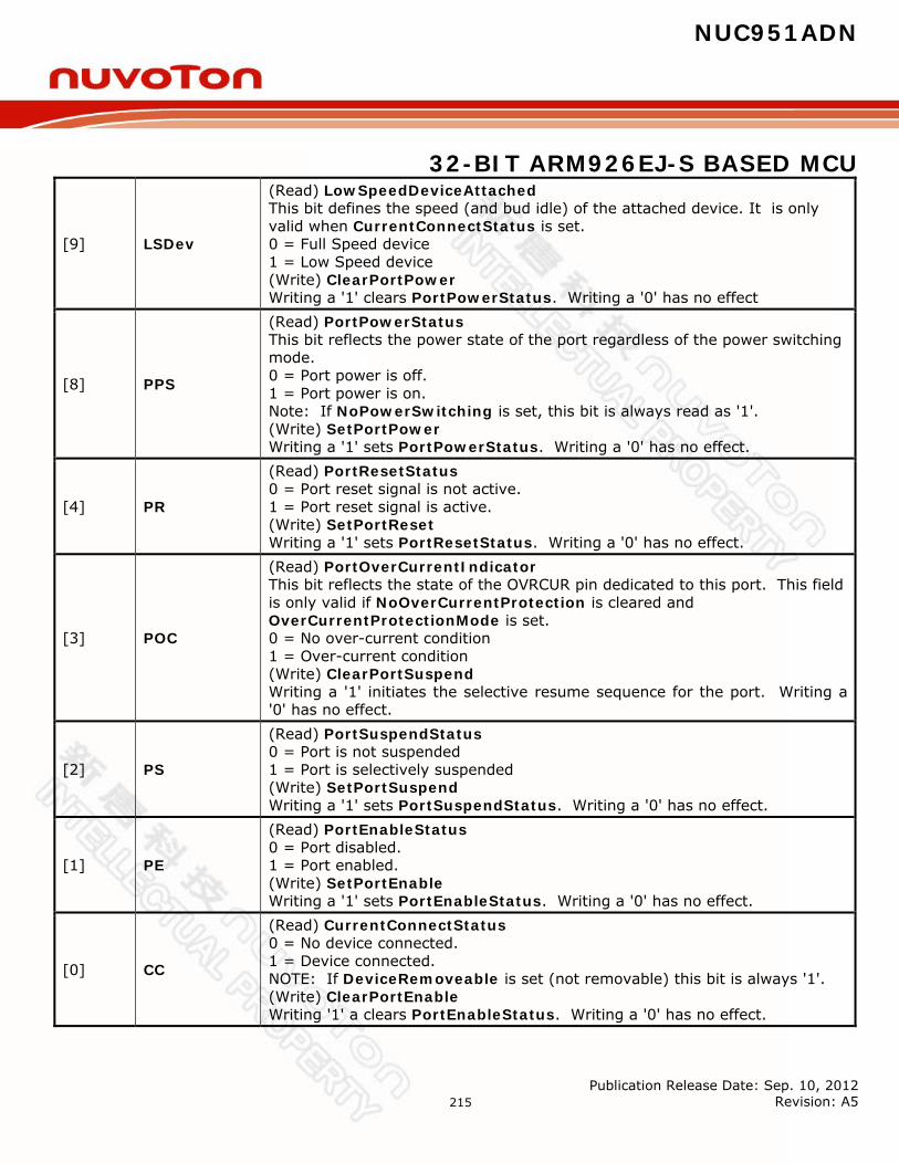
NUC951ADN
32-BIT ARM926EJ-S BASED MCU
Publication Release Date: Sep. 10, 2012 Revision: A5
215
[9] LSDev
(Read) LowSpeedDeviceAttached This bit defines the speed (and bud idle) of the attached device. It is only valid when CurrentConnectStatus is set. 0 = Full Speed device 1 = Low Speed device (Write) ClearPortPower Writing a '1' clears PortPowerStatus. Writing a '0' has no effect
[8] PPS
(Read) PortPowerStatus This bit reflects the power state of the port regardless of the power switching mode. 0 = Port power is off. 1 = Port power is on. Note: If NoPowerSwitching is set, this bit is always read as '1'. (Write) SetPortPower Writing a '1' sets PortPowerStatus. Writing a '0' has no effect.
[4] PR
(Read) PortResetStatus 0 = Port reset signal is not active. 1 = Port reset signal is active. (Write) SetPortReset Writing a '1' sets PortResetStatus. Writing a '0' has no effect.
[3] POC
(Read) PortOverCurrentIndicator This bit reflects the state of the OVRCUR pin dedicated to this port. This field is only valid if NoOverCurrentProtection is cleared and OverCurrentProtectionMode is set. 0 = No over-current condition 1 = Over-current condition (Write) ClearPortSuspend Writing a '1' initiates the selective resume sequence for the port. Writing a '0' has no effect.
[2] PS
(Read) PortSuspendStatus 0 = Port is not suspended 1 = Port is selectively suspended (Write) SetPortSuspend Writing a '1' sets PortSuspendStatus. Writing a '0' has no effect.
[1] PE
(Read) PortEnableStatus 0 = Port disabled. 1 = Port enabled. (Write) SetPortEnable Writing a '1' sets PortEnableStatus. Writing a '0' has no effect.
[0] CC
(Read) CurrentConnectStatus 0 = No device connected. 1 = Device connected. NOTE: If DeviceRemoveable is set (not removable) this bit is always '1'. (Write) ClearPortEnable Writing '1' a clears PortEnableStatus. Writing a '0' has no effect.
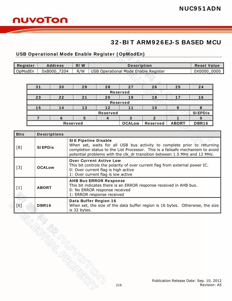
NUC951ADN
32-BIT ARM926EJ-S BASED MCU
Publication Release Date: Sep. 10, 2012 Revision: A5
216
USB Operational Mode Enable Register (OpModEn)
Register Address R/W Description Reset Value OpModEn 0xB000_7204 R/W USB Operational Mode Enable Register 0X0000_0000
31 30 29 28 27 26 25 24 Reserved
23 22 21 20 19 18 17 16 Reserved
15 14 13 12 11 10 9 8 Reserved SIEPDis
7 6 5 4 3 2 1 0 Reserved OCALow Reserved ABORT DBR16
Bits Descriptions
[8] SIEPDis
SIE Pipeline Disable When set, waits for all USB bus activity to complete prior to returning completion status to the List Processor. This is a failsafe mechanism to avoid potential problems with the clk_dr transition between 1.5 MHz and 12 MHz.
[3] OCALow
Over Current Active Low This bit controls the polarity of over current flag from external power IC. 0: Over current flag is high active 1: Over current flag is low active
[1] ABORT
AHB Bus ERROR Response This bit indicates there is an ERROR response received in AHB bus. 0: No ERROR response received 1: ERROR response received
[0] DBR16 Data Buffer Region 16 When set, the size of the data buffer region is 16 bytes. Otherwise, the size is 32 bytes.
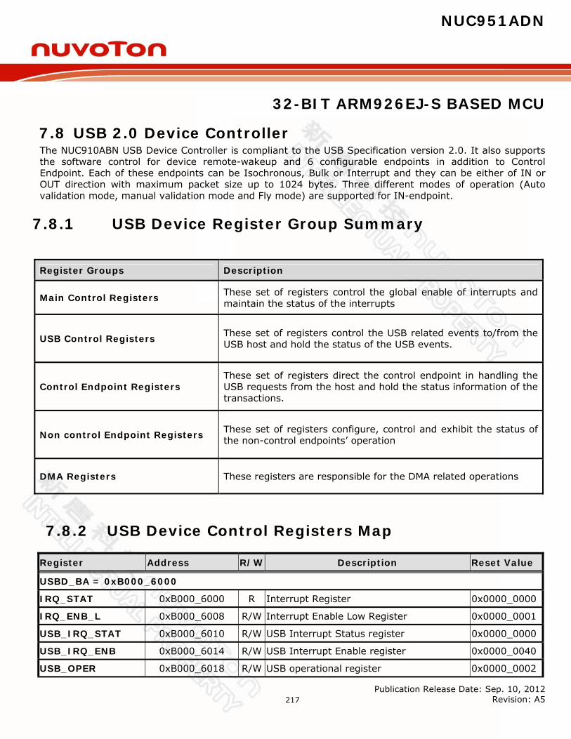
NUC951ADN
32-BIT ARM926EJ-S BASED MCU
Publication Release Date: Sep. 10, 2012 Revision: A5
217
7.8 USB 2.0 Device Controller The NUC910ABN USB Device Controller is compliant to the USB Specification version 2.0. It also supports the software control for device remote-wakeup and 6 configurable endpoints in addition to Control Endpoint. Each of these endpoints can be Isochronous, Bulk or Interrupt and they can be either of IN or OUT direction with maximum packet size up to 1024 bytes. Three different modes of operation (Auto validation mode, manual validation mode and Fly mode) are supported for IN-endpoint.
7.8.1 USB Device Register Group Summary
Register Groups Description
Main Control Registers These set of registers control the global enable of interrupts and maintain the status of the interrupts
USB Control Registers These set of registers control the USB related events to/from the USB host and hold the status of the USB events.
Control Endpoint Registers These set of registers direct the control endpoint in handling the USB requests from the host and hold the status information of the transactions.
Non control Endpoint Registers These set of registers configure, control and exhibit the status of the non-control endpoints’ operation
DMA Registers These registers are responsible for the DMA related operations
7.8.2 USB Device Control Registers Map
Register Address R/W Description Reset Value
USBD_BA = 0xB000_6000
IRQ_STAT 0xB000_6000 R Interrupt Register 0x0000_0000
IRQ_ENB_L 0xB000_6008 R/W Interrupt Enable Low Register 0x0000_0001
USB_IRQ_STAT 0xB000_6010 R/W USB Interrupt Status register 0x0000_0000
USB_IRQ_ENB 0xB000_6014 R/W USB Interrupt Enable register 0x0000_0040
USB_OPER 0xB000_6018 R/W USB operational register 0x0000_0002
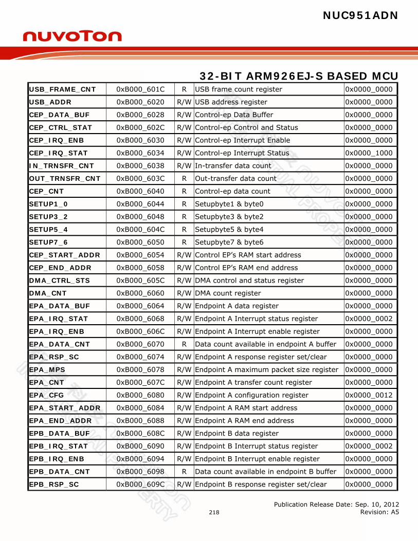
NUC951ADN
32-BIT ARM926EJ-S BASED MCU
Publication Release Date: Sep. 10, 2012 Revision: A5
218
USB_FRAME_CNT 0xB000_601C R USB frame count register 0x0000_0000
USB_ADDR 0xB000_6020 R/W USB address register 0x0000_0000
CEP_DATA_BUF 0xB000_6028 R/W Control-ep Data Buffer 0x0000_0000
CEP_CTRL_STAT 0xB000_602C R/W Control-ep Control and Status 0x0000_0000
CEP_IRQ_ENB 0xB000_6030 R/W Control-ep Interrupt Enable 0x0000_0000
CEP_IRQ_STAT 0xB000_6034 R/W Control-ep Interrupt Status 0x0000_1000
IN_TRNSFR_CNT 0xB000_6038 R/W In-transfer data count 0x0000_0000
OUT_TRNSFR_CNT 0xB000_603C R Out-transfer data count 0x0000_0000
CEP_CNT 0xB000_6040 R Control-ep data count 0x0000_0000
SETUP1_0 0xB000_6044 R Setupbyte1 & byte0 0x0000_0000
SETUP3_2 0xB000_6048 R Setupbyte3 & byte2 0x0000_0000
SETUP5_4 0xB000_604C R Setupbyte5 & byte4 0x0000_0000
SETUP7_6 0xB000_6050 R Setupbyte7 & byte6 0x0000_0000
CEP_START_ADDR 0xB000_6054 R/W Control EP’s RAM start address 0x0000_0000
CEP_END_ADDR 0xB000_6058 R/W Control EP’s RAM end address 0x0000_0000
DMA_CTRL_STS 0xB000_605C R/W DMA control and status register 0x0000_0000
DMA_CNT 0xB000_6060 R/W DMA count register 0x0000_0000
EPA_DATA_BUF 0xB000_6064 R/W Endpoint A data register 0x0000_0000
EPA_IRQ_STAT 0xB000_6068 R/W Endpoint A Interrupt status register 0x0000_0002
EPA_IRQ_ENB 0xB000_606C R/W Endpoint A Interrupt enable register 0x0000_0000
EPA_DATA_CNT 0xB000_6070 R Data count available in endpoint A buffer 0x0000_0000
EPA_RSP_SC 0xB000_6074 R/W Endpoint A response register set/clear 0x0000_0000
EPA_MPS 0xB000_6078 R/W Endpoint A maximum packet size register 0x0000_0000
EPA_CNT 0xB000_607C R/W Endpoint A transfer count register 0x0000_0000
EPA_CFG 0xB000_6080 R/W Endpoint A configuration register 0x0000_0012
EPA_START_ADDR 0xB000_6084 R/W Endpoint A RAM start address 0x0000_0000
EPA_END_ADDR 0xB000_6088 R/W Endpoint A RAM end address 0x0000_0000
EPB_DATA_BUF 0xB000_608C R/W Endpoint B data register 0x0000_0000
EPB_IRQ_STAT 0xB000_6090 R/W Endpoint B Interrupt status register 0x0000_0002
EPB_IRQ_ENB 0xB000_6094 R/W Endpoint B Interrupt enable register 0x0000_0000
EPB_DATA_CNT 0xB000_6098 R Data count available in endpoint B buffer 0x0000_0000
EPB_RSP_SC 0xB000_609C R/W Endpoint B response register set/clear 0x0000_0000
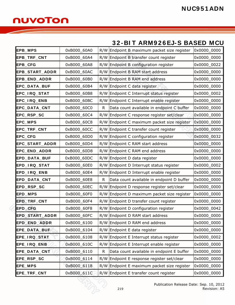
NUC951ADN
32-BIT ARM926EJ-S BASED MCU
Publication Release Date: Sep. 10, 2012 Revision: A5
219
EPB_MPS 0xB000_60A0 R/W Endpoint B maximum packet size register 0x0000_0000
EPB_TRF_CNT 0xB000_60A4 R/W Endpoint B transfer count register 0x0000_0000
EPB_CFG 0xB000_60A8 R/W Endpoint B configuration register 0x0000_0022
EPB_START_ADDR 0xB000_60AC R/W Endpoint B RAM start address 0x0000_0000
EPB_END_ADDR 0xB000_60B0 R/W Endpoint B RAM end address 0x0000_0000
EPC_DATA_BUF 0xB000_60B4 R/W Endpoint C data register 0x0000_0000
EPC_IRQ_STAT 0xB000_60B8 R/W Endpoint C Interrupt status register 0x0000_0002
EPC_IRQ_ENB 0xB000_60BC R/W Endpoint C Interrupt enable register 0x0000_0000
EPC_DATA_CNT 0xB000_60C0 R Data count available in endpoint C buffer 0x0000_0000
EPC_RSP_SC 0xB000_60C4 R/W Endpoint C response register set/clear 0x0000_0000
EPC_MPS 0xB000_60C8 R/W Endpoint C maximum packet size register 0x0000_0000
EPC_TRF_CNT 0xB000_60CC R/W Endpoint C transfer count register 0x0000_0000
EPC_CFG 0xB000_60D0 R/W Endpoint C configuration register 0x0000_0032
EPC_START_ADDR 0xB000_60D4 R/W Endpoint C RAM start address 0x0000_0000
EPC_END_ADDR 0xB000_60D8 R/W Endpoint C RAM end address 0x0000_0000
EPD_DATA_BUF 0xB000_60DC R/W Endpoint D data register 0x0000_0000
EPD_IRQ_STAT 0xB000_60E0 R/W Endpoint D Interrupt status register 0x0000_0002
EPD_IRQ_ENB 0xB000_60E4 R/W Endpoint D Interrupt enable register 0x0000_0000
EPD_DATA_CNT 0xB000_60E8 R Data count available in endpoint D buffer 0x0000_0000
EPD_RSP_SC 0xB000_60EC R/W Endpoint D response register set/clear 0x0000_0000
EPD_MPS 0xB000_60F0 R/W Endpoint D maximum packet size register 0x0000_0000
EPD_TRF_CNT 0xB000_60F4 R/W Endpoint D transfer count register 0x0000_0000
EPD_CFG 0xB000_60F8 R/W Endpoint D configuration register 0x0000_0042
EPD_START_ADDR 0xB000_60FC R/W Endpoint D RAM start address 0x0000_0000
EPD_END_ADDR 0xB000_6100 R/W Endpoint D RAM end address 0x0000_0000
EPE_DATA_BUF 0xB000_6104 R/W Endpoint E data register 0x0000_0000
EPE_IRQ_STAT 0xB000_6108 R/W Endpoint E Interrupt status register 0x0000_0002
EPE_IRQ_ENB 0xB000_610C R/W Endpoint E Interrupt enable register 0x0000_0000
EPE_DATA_CNT 0xB000_6110 R Data count available in endpoint E buffer 0x0000_0000
EPE_RSP_SC 0xB000_6114 R/W Endpoint E response register set/clear 0x0000_0000
EPE_MPS 0xB000_6118 R/W Endpoint E maximum packet size register 0x0000_0000
EPE_TRF_CNT 0xB000_611C R/W Endpoint E transfer count register 0x0000_0000

NUC951ADN
32-BIT ARM926EJ-S BASED MCU
Publication Release Date: Sep. 10, 2012 Revision: A5
220
EPE_CFG 0xB000_6120 R/W Endpoint E configuration register 0x0000_0052
EPE_START_ADDR 0xB000_6124 R/W Endpoint E RAM start address 0x0000_0000
EPE_END_ADDR 0xB000_6128 R/W Endpoint E RAM end address 0x0000_0000
EPF_DATA_BUF 0xB000_612C R/W Endpoint F data register 0x0000_0000
EPF_IRQ_STAT 0xB000_6130 R/W Endpoint F Interrupt status register 0x0000_0002
EPF_IRQ_ENB 0xB000_6134 R/W Endpoint F Interrupt enable register 0x0000_0000
EPF_DATA_CNT 0xB000_6138 R Data count available in endpoint F buffer 0x0000_0000
EPF_RSP_SC 0xB000_613C R/W Endpoint F response register set/clear 0x0000_0000
EPF_MPS 0xB000_6140 R/W Endpoint F maximum packet size register 0x0000_0000
EPF_TRF_CNT 0xB000_6144 R/W Endpoint F transfer count register 0x0000_0000
EPF_CFG 0xB000_6148 R/W Endpoint F configuration register 0x0000_0062
EPF_START_ADDR 0xB000_614C R/W Endpoint F RAM start address 0x0000_0000
EPF_END_ADDR 0xB000_6150 R/W Endpoint F RAM end address 0x0000_0000
USB_DMA_ADDR 0xB000_6700 R/W AHB_DMA address register 0x0000_0000
USB_PHY_CTL 0xB000_6704 R/W USB PHY control register 0x0000_0060
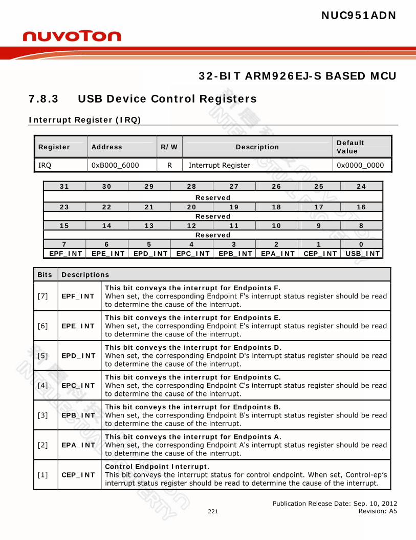
NUC951ADN
32-BIT ARM926EJ-S BASED MCU
Publication Release Date: Sep. 10, 2012 Revision: A5
221
7.8.3 USB Device Control Registers
Interrupt Register (IRQ)
Register Address R/W Description Default Value
IRQ 0xB000_6000 R Interrupt Register 0x0000_0000
31 30 29 28 27 26 25 24
Reserved 23 22 21 20 19 18 17 16
Reserved 15 14 13 12 11 10 9 8
Reserved 7 6 5 4 3 2 1 0
EPF_INT EPE_INT EPD_INT EPC_INT EPB_INT EPA_INT CEP_INT USB_INT
Bits Descriptions
[7] EPF_INT This bit conveys the interrupt for Endpoints F. When set, the corresponding Endpoint F's interrupt status register should be read to determine the cause of the interrupt.
[6] EPE_INT This bit conveys the interrupt for Endpoints E. When set, the corresponding Endpoint E's interrupt status register should be read to determine the cause of the interrupt.
[5] EPD_INT This bit conveys the interrupt for Endpoints D. When set, the corresponding Endpoint D's interrupt status register should be read to determine the cause of the interrupt.
[4] EPC_INT This bit conveys the interrupt for Endpoints C. When set, the corresponding Endpoint C's interrupt status register should be read to determine the cause of the interrupt.
[3] EPB_INT This bit conveys the interrupt for Endpoints B. When set, the corresponding Endpoint B's interrupt status register should be read to determine the cause of the interrupt.
[2] EPA_INT This bit conveys the interrupt for Endpoints A. When set, the corresponding Endpoint A's interrupt status register should be read to determine the cause of the interrupt.
[1] CEP_INT Control Endpoint Interrupt. This bit conveys the interrupt status for control endpoint. When set, Control-ep’s interrupt status register should be read to determine the cause of the interrupt.

NUC951ADN
32-BIT ARM926EJ-S BASED MCU
Publication Release Date: Sep. 10, 2012 Revision: A5
222
[0] USB_INT USB Interrupt. The interrupt status for USB specific events endpoint. When set, USB interrupt status register should be read to determine the cause of the interrupt.
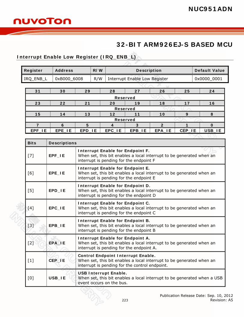
NUC951ADN
32-BIT ARM926EJ-S BASED MCU
Publication Release Date: Sep. 10, 2012 Revision: A5
223
Interrupt Enable Low Register (IRQ_ENB_L)
Register Address R/W Description Default Value
IRQ_ENB_L 0xB000_6008 R/W Interrupt Enable Low Register 0x0000_0001
31 30 29 28 27 26 25 24
Reserved 23 22 21 20 19 18 17 16
Reserved 15 14 13 12 11 10 9 8
Reserved 7 6 5 4 3 2 1 0
EPF_IE EPE_IE EPD_IE EPC_IE EPB_IE EPA_IE CEP_IE USB_IE
Bits Descriptions
[7] EPF_IE Interrupt Enable for Endpoint F. When set, this bit enables a local interrupt to be generated when an interrupt is pending for the endpoint F
[6] EPE_IE Interrupt Enable for Endpoint E. When set, this bit enables a local interrupt to be generated when an interrupt is pending for the endpoint E
[5] EPD_IE Interrupt Enable for Endpoint D. When set, this bit enables a local interrupt to be generated when an interrupt is pending for the endpoint D
[4] EPC_IE Interrupt Enable for Endpoint C. When set, this bit enables a local interrupt to be generated when an interrupt is pending for the endpoint C
[3] EPB_IE Interrupt Enable for Endpoint B. When set, this bit enables a local interrupt to be generated when an interrupt is pending for the endpoint B
[2] EPA_IE Interrupt Enable for Endpoint A. When set, this bit enables a local interrupt to be generated when an interrupt is pending for the endpoint A.
[1] CEP_IE Control Endpoint Interrupt Enable. When set, this bit enables a local interrupt to be generated when an interrupt is pending for the control endpoint.
[0] USB_IE USB Interrupt Enable. When set, this bit enables a local interrupt to be generated when a USB event occurs on the bus.
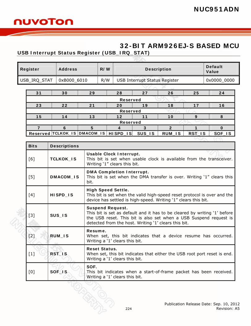
NUC951ADN
32-BIT ARM926EJ-S BASED MCU
Publication Release Date: Sep. 10, 2012 Revision: A5
224
USB Interrupt Status Register (USB_IRQ_STAT)
Register Address R/W Description Default Value
USB_IRQ_STAT 0xB000_6010 R/W USB Interrupt Status Register 0x0000_0000
31 30 29 28 27 26 25 24
Reserved 23 22 21 20 19 18 17 16
Reserved 15 14 13 12 11 10 9 8
Reserved 7 6 5 4 3 2 1 0
Reserved TCLKOK_IS DMACOM_IS HISPD_IS SUS_IS RUM_IS RST_IS SOF_IS
Bits Descriptions
[6] TCLKOK_IS Usable Clock Interrupt. This bit is set when usable clock is available from the transceiver. Writing ‘1” clears this bit.
[5] DMACOM_IS DMA Completion Interrupt. This bit is set when the DMA transfer is over. Writing ‘1” clears this bit.
[4] HISPD_IS High Speed Settle. This bit is set when the valid high-speed reset protocol is over and the device has settled is high-speed. Writing ‘1” clears this bit.
[3] SUS_IS
Suspend Request. This bit is set as default and it has to be cleared by writing ‘1’ before the USB reset. This bit is also set when a USB Suspend request is detected from the host. Writing ‘1’ clears this bit.
[2] RUM_IS Resume. When set, this bit indicates that a device resume has occurred. Writing a ‘1’ clears this bit.
[1] RST_IS Reset Status. When set, this bit indicates that either the USB root port reset is end. Writing a ‘1’ clears this bit.
[0] SOF_IS SOF. This bit indicates when a start-of-frame packet has been received. Writing a ‘1’ clears this bit.

NUC951ADN
32-BIT ARM926EJ-S BASED MCU
Publication Release Date: Sep. 10, 2012 Revision: A5
225
USB Interrupt Enable Register (USB_IRQ_ENB)
Register Address R/W Description Default Value
USB_IRQ_ENB 0xB000_6014 R/W USB Interrupt Enable Register 0x0000_0040
31 30 29 28 27 26 25 24
Reserved 23 22 21 20 19 18 17 16
Reserved 15 14 13 12 11 10 9 8
Reserved 7 6 5 4 3 2 1 0
Reserved TCLKOK_IE DMACOM_IE HISPD_IE SUS_IE RUM_IE RST_IE SOF_IE Bits Descriptions
[6] TCLKOK_IE Usable Clock Interrupt. This bit enables the usable clock interrupt.
[5] DMACOM_IE DMA Completion Interrupt. This bit enables the DMA completion interrupt
[4] HISPD_IE High Speed Settle. This bit enables the high-speed settle interrupt.
[3] SUS_IE Suspend Request. This bit enables the Suspend interrupt.
[2] RUM_IE Resume. This bit enables the Resume interrupt.
[1] RST_IE Reset Status. This bit enables the USB-Reset interrupt.
[0] SOF_IE SOF Interrupt. This bit enables the SOF interrupt.
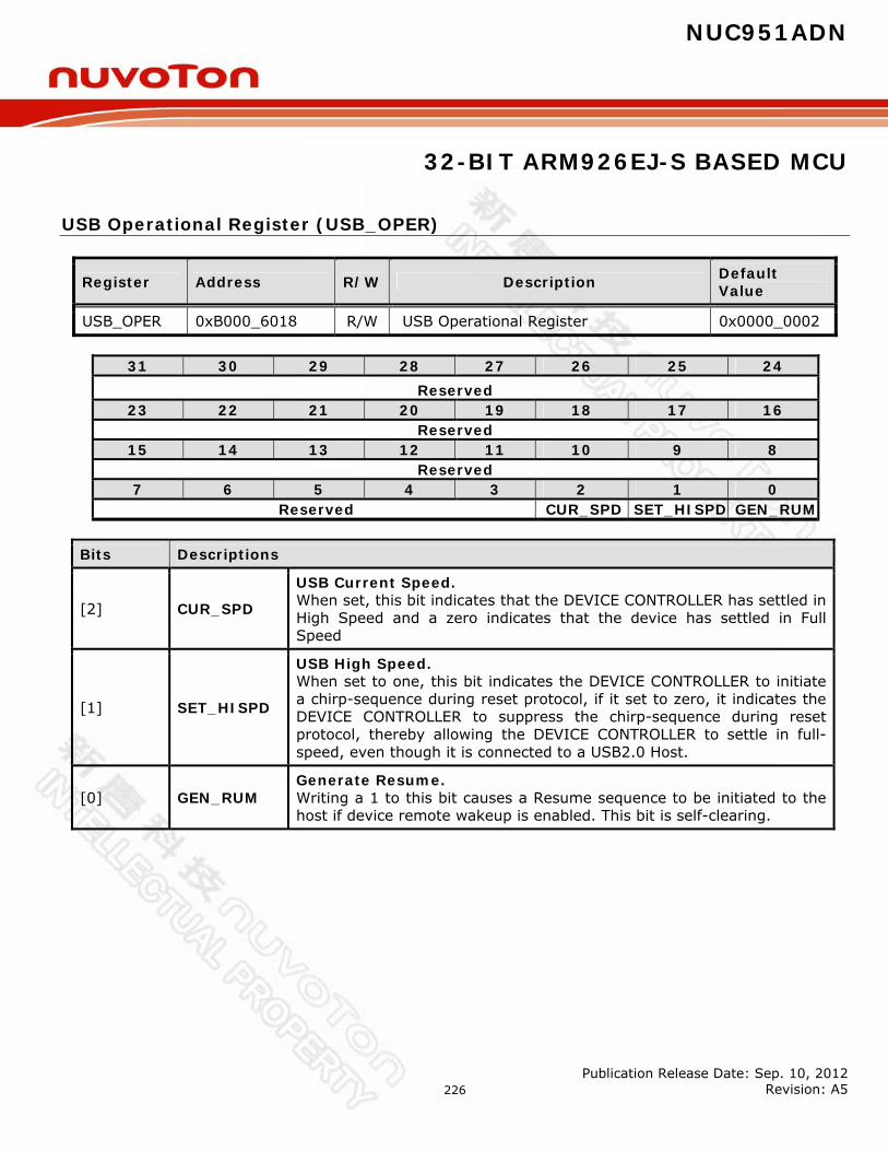
NUC951ADN
32-BIT ARM926EJ-S BASED MCU
Publication Release Date: Sep. 10, 2012 Revision: A5
226
USB Operational Register (USB_OPER)
Register Address R/W Description Default Value
USB_OPER 0xB000_6018 R/W USB Operational Register 0x0000_0002
31 30 29 28 27 26 25 24
Reserved 23 22 21 20 19 18 17 16
Reserved 15 14 13 12 11 10 9 8
Reserved 7 6 5 4 3 2 1 0
Reserved CUR_SPD SET_HISPD GEN_RUM
Bits Descriptions
[2] CUR_SPD
USB Current Speed. When set, this bit indicates that the DEVICE CONTROLLER has settled in High Speed and a zero indicates that the device has settled in Full Speed
[1] SET_HISPD
USB High Speed. When set to one, this bit indicates the DEVICE CONTROLLER to initiate a chirp-sequence during reset protocol, if it set to zero, it indicates the DEVICE CONTROLLER to suppress the chirp-sequence during reset protocol, thereby allowing the DEVICE CONTROLLER to settle in full-speed, even though it is connected to a USB2.0 Host.
[0] GEN_RUM Generate Resume. Writing a 1 to this bit causes a Resume sequence to be initiated to the host if device remote wakeup is enabled. This bit is self-clearing.

NUC951ADN
32-BIT ARM926EJ-S BASED MCU
Publication Release Date: Sep. 10, 2012 Revision: A5
227
USB Frame Count Register (USB_FRAME_CNT)
Register Address R/W Description Default Value
USB_FRAME_CNT 0xB000_601C R USB Frame Count Register 0x0000_0000
31 30 29 28 27 26 25 24
Reserved 23 22 21 20 19 18 17 16
Reserved 15 14 13 12 11 10 9 8
Reserved FRAME_CNT 7 6 5 4 3 2 1 0
FRAME_CNT MFRAME_CNT Bits Descriptions
[13:3] FRAME_CNT FRAME COUNTER. This field contains the frame count from the most recent start-of-frame packet.
[2:0] MFRAME_CNT MICRO FRAME COUNTER. This field contains the micro-frame number for the frame number in the frame counter field.
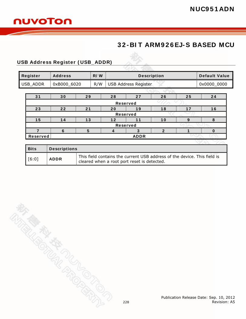
NUC951ADN
32-BIT ARM926EJ-S BASED MCU
Publication Release Date: Sep. 10, 2012 Revision: A5
228
USB Address Register (USB_ADDR)
Register Address R/W Description Default Value
USB_ADDR 0xB000_6020 R/W USB Address Register 0x0000_0000
31 30 29 28 27 26 25 24
Reserved 23 22 21 20 19 18 17 16
Reserved 15 14 13 12 11 10 9 8
Reserved 7 6 5 4 3 2 1 0
Reserved ADDR
Bits Descriptions
[6:0] ADDR This field contains the current USB address of the device. This field is cleared when a root port reset is detected.
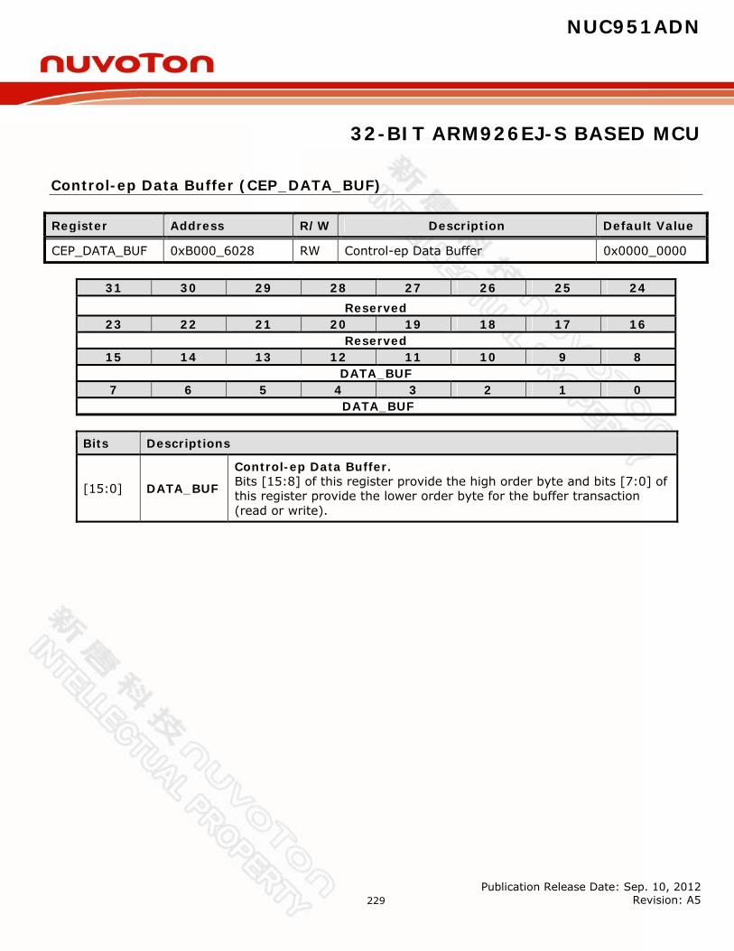
NUC951ADN
32-BIT ARM926EJ-S BASED MCU
Publication Release Date: Sep. 10, 2012 Revision: A5
229
Control-ep Data Buffer (CEP_DATA_BUF)
Register Address R/W Description Default Value
CEP_DATA_BUF 0xB000_6028 RW Control-ep Data Buffer 0x0000_0000
31 30 29 28 27 26 25 24
Reserved 23 22 21 20 19 18 17 16
Reserved 15 14 13 12 11 10 9 8
DATA_BUF 7 6 5 4 3 2 1 0
DATA_BUF
Bits Descriptions
[15:0] DATA_BUF
Control-ep Data Buffer. Bits [15:8] of this register provide the high order byte and bits [7:0] of this register provide the lower order byte for the buffer transaction (read or write).
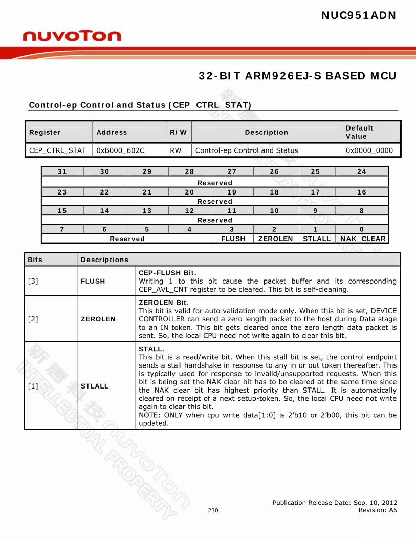
NUC951ADN
32-BIT ARM926EJ-S BASED MCU
Publication Release Date: Sep. 10, 2012 Revision: A5
230
Control-ep Control and Status (CEP_CTRL_STAT)
Register Address R/W Description Default Value
CEP_CTRL_STAT 0xB000_602C RW Control-ep Control and Status 0x0000_0000
31 30 29 28 27 26 25 24
Reserved 23 22 21 20 19 18 17 16
Reserved 15 14 13 12 11 10 9 8
Reserved 7 6 5 4 3 2 1 0
Reserved FLUSH ZEROLEN STLALL NAK_CLEAR Bits Descriptions
[3] FLUSH CEP-FLUSH Bit. Writing 1 to this bit cause the packet buffer and its corresponding CEP_AVL_CNT register to be cleared. This bit is self-cleaning.
[2] ZEROLEN
ZEROLEN Bit. This bit is valid for auto validation mode only. When this bit is set, DEVICE CONTROLLER can send a zero length packet to the host during Data stage to an IN token. This bit gets cleared once the zero length data packet is sent. So, the local CPU need not write again to clear this bit.
[1] STLALL
STALL. This bit is a read/write bit. When this stall bit is set, the control endpoint sends a stall handshake in response to any in or out token thereafter. This is typically used for response to invalid/unsupported requests. When this bit is being set the NAK clear bit has to be cleared at the same time since the NAK clear bit has highest priority than STALL. It is automatically cleared on receipt of a next setup-token. So, the local CPU need not write again to clear this bit. NOTE: ONLY when cpu write data[1:0] is 2’b10 or 2’b00, this bit can be updated.
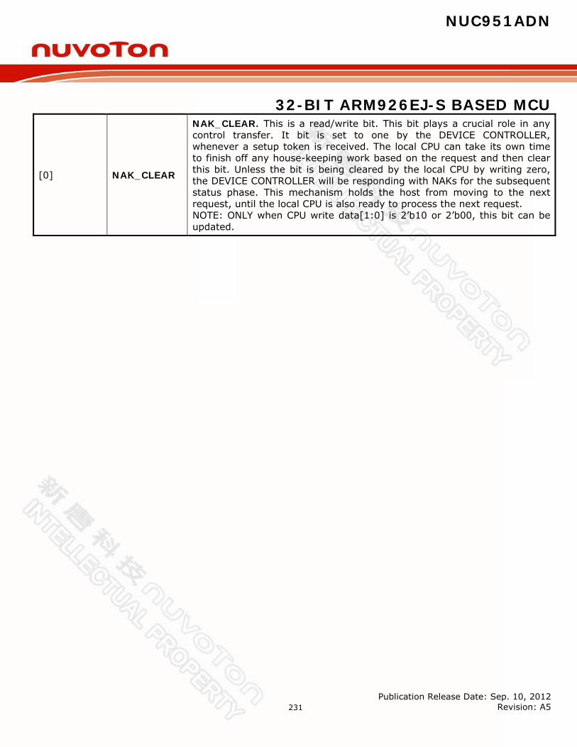
NUC951ADN
32-BIT ARM926EJ-S BASED MCU
Publication Release Date: Sep. 10, 2012 Revision: A5
231
[0] NAK_CLEAR
NAK_CLEAR. This is a read/write bit. This bit plays a crucial role in any control transfer. It bit is set to one by the DEVICE CONTROLLER, whenever a setup token is received. The local CPU can take its own time to finish off any house-keeping work based on the request and then clear this bit. Unless the bit is being cleared by the local CPU by writing zero, the DEVICE CONTROLLER will be responding with NAKs for the subsequent status phase. This mechanism holds the host from moving to the next request, until the local CPU is also ready to process the next request. NOTE: ONLY when CPU write data[1:0] is 2’b10 or 2’b00, this bit can be updated.
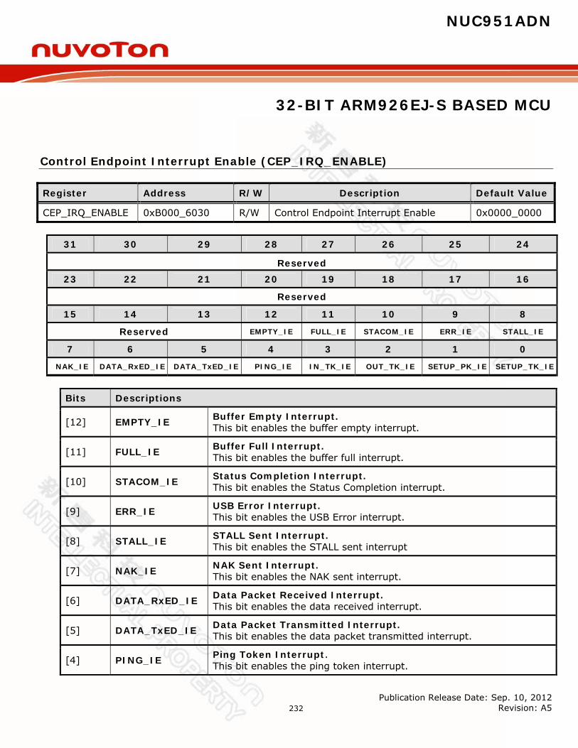
NUC951ADN
32-BIT ARM926EJ-S BASED MCU
Publication Release Date: Sep. 10, 2012 Revision: A5
232
Control Endpoint Interrupt Enable (CEP_IRQ_ENABLE)
Register Address R/W Description Default Value
CEP_IRQ_ENABLE 0xB000_6030 R/W Control Endpoint Interrupt Enable 0x0000_0000
31 30 29 28 27 26 25 24
Reserved 23 22 21 20 19 18 17 16
Reserved
15 14 13 12 11 10 9 8
Reserved EMPTY_IE FULL_IE STACOM_IE ERR_IE STALL_IE
7 6 5 4 3 2 1 0
NAK_IE DATA_RxED_IE DATA_TxED_IE PING_IE IN_TK_IE OUT_TK_IE SETUP_PK_IE SETUP_TK_IE
Bits Descriptions
[12] EMPTY_IE Buffer Empty Interrupt. This bit enables the buffer empty interrupt.
[11] FULL_IE Buffer Full Interrupt. This bit enables the buffer full interrupt.
[10] STACOM_IE Status Completion Interrupt. This bit enables the Status Completion interrupt.
[9] ERR_IE USB Error Interrupt. This bit enables the USB Error interrupt.
[8] STALL_IE STALL Sent Interrupt. This bit enables the STALL sent interrupt
[7] NAK_IE NAK Sent Interrupt. This bit enables the NAK sent interrupt.
[6] DATA_RxED_IE Data Packet Received Interrupt. This bit enables the data received interrupt.
[5] DATA_TxED_IE Data Packet Transmitted Interrupt. This bit enables the data packet transmitted interrupt.
[4] PING_IE Ping Token Interrupt. This bit enables the ping token interrupt.
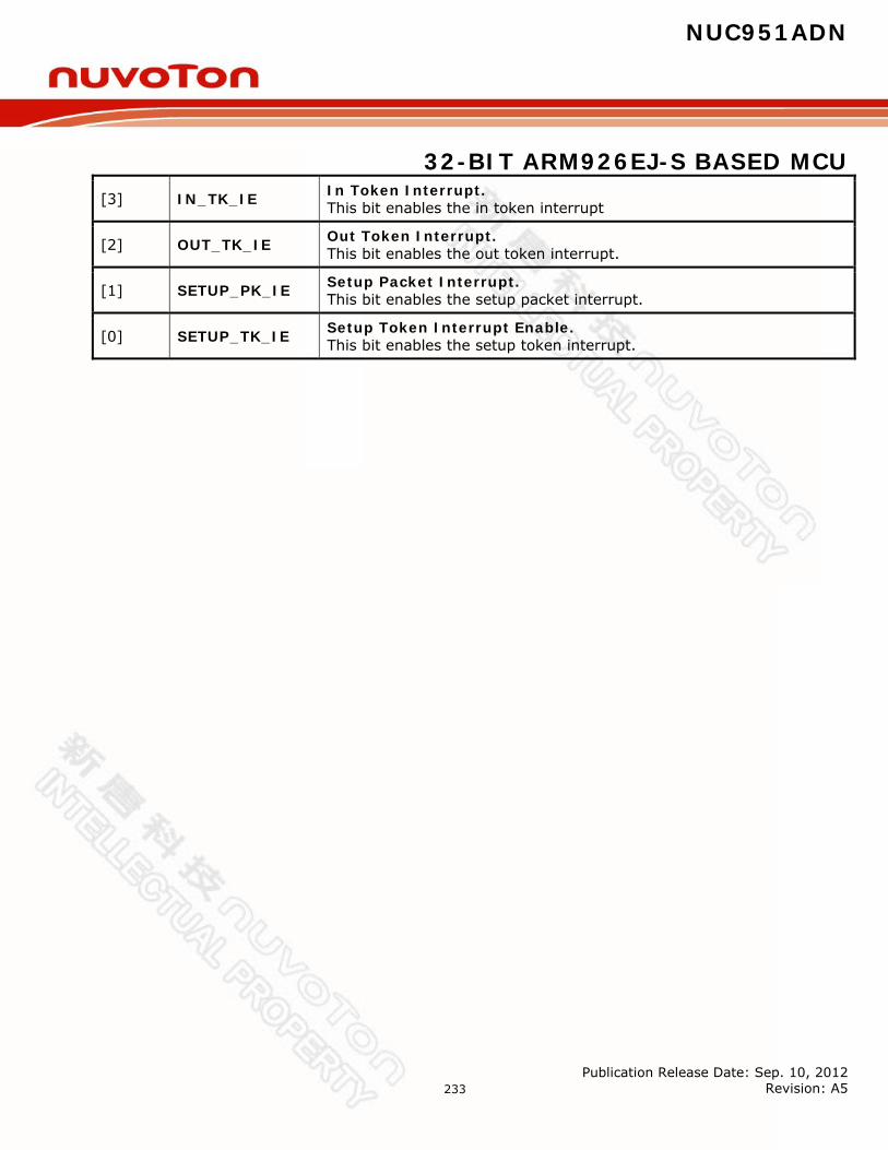
NUC951ADN
32-BIT ARM926EJ-S BASED MCU
Publication Release Date: Sep. 10, 2012 Revision: A5
233
[3] IN_TK_IE In Token Interrupt. This bit enables the in token interrupt
[2] OUT_TK_IE Out Token Interrupt. This bit enables the out token interrupt.
[1] SETUP_PK_IE Setup Packet Interrupt. This bit enables the setup packet interrupt.
[0] SETUP_TK_IE Setup Token Interrupt Enable. This bit enables the setup token interrupt.
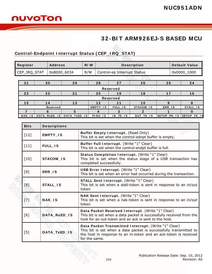
NUC951ADN
32-BIT ARM926EJ-S BASED MCU
Publication Release Date: Sep. 10, 2012 Revision: A5
234
Control-Endpoint Interrupt Status (CEP_IRQ_STAT)
Register Address R/W Description Default Value
CEP_IRQ_STAT 0xB000_6034 R/W Control-ep Interrupt Status 0x0000_1000
31 30 29 28 27 26 25 24
Reserved 23 22 21 20 19 18 17 16
Reserved 15 14 13 12 11 10 9 8
Reserved EMPTY_IS FULL_IS STACOM_IS ERR_IS STALL_IS 7 6 5 4 3 2 1 0
NAK_IS DATA_RxED_IS DATA_TxED_IS PING_IS IN_TK_IS OUT_TK_IS SETUP_PK_IS SETUP_TK_IS
Bits Descriptions
[12] EMPTY_IS Buffer Empty Interrupt. (Read Only) This bit is set when the control-ednpt buffer is empty.
[11] FULL_IS Buffer Full Interrupt. (Write “1” Clear) This bit is set when the control-endpt buffer is full.
[10] STACOM_IS Status Completion Interrupt. (Write “1” Clear) This bit is set when the status stage of a USB transaction has completed successfully.
[9] ERR_IS USB Error Interrupt. (Write “1” Clear) This bit is set when an error had occurred during the transaction.
[8] STALL_IS STALL Sent Interrupt. (Write “1” Clear) This bit is set when a stall-token is sent in response to an in/out token
[7] NAK_IS NAK Sent Interrupt. (Write “1” Clear) This bit is set when a nak-token is sent in response to an in/out token
[6] DATA_RxED_IS Data Packet Received Interrupt. (Write “1” Clear) This bit is set when a data packet is successfully received from the host for an out-token and an ack is sent to the host.
[5] DATA_TxED_IS
Data Packet Transmitted Interrupt. (Write “1” Clear) This bit is set when a data packet is successfully transmitted to the host in response to an in-token and an ack-token is received for the same.
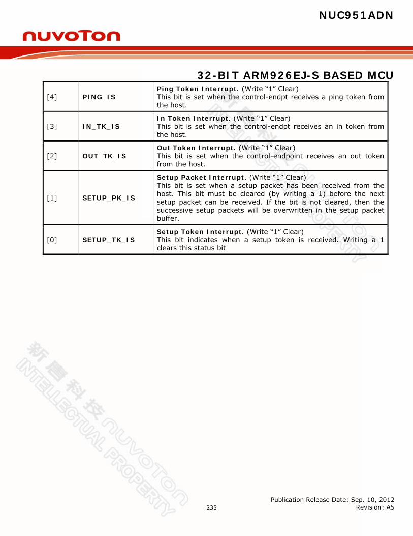
NUC951ADN
32-BIT ARM926EJ-S BASED MCU
Publication Release Date: Sep. 10, 2012 Revision: A5
235
[4] PING_IS Ping Token Interrupt. (Write “1” Clear) This bit is set when the control-endpt receives a ping token from the host.
[3] IN_TK_IS In Token Interrupt. (Write “1” Clear) This bit is set when the control-endpt receives an in token from the host.
[2] OUT_TK_IS Out Token Interrupt. (Write “1” Clear) This bit is set when the control-endpoint receives an out token from the host.
[1] SETUP_PK_IS
Setup Packet Interrupt. (Write “1” Clear) This bit is set when a setup packet has been received from the host. This bit must be cleared (by writing a 1) before the next setup packet can be received. If the bit is not cleared, then the successive setup packets will be overwritten in the setup packet buffer.
[0] SETUP_TK_IS Setup Token Interrupt. (Write “1” Clear) This bit indicates when a setup token is received. Writing a 1 clears this status bit
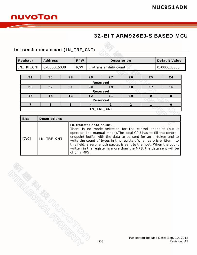
NUC951ADN
32-BIT ARM926EJ-S BASED MCU
Publication Release Date: Sep. 10, 2012 Revision: A5
236
In-transfer data count (IN_TRF_CNT)
Register Address R/W Description Default Value
IN_TRF_CNT 0xB000_6038 R/W In-transfer data count 0x0000_0000
31 30 29 28 27 26 25 24
Reserved 23 22 21 20 19 18 17 16
Reserved 15 14 13 12 11 10 9 8
Reserved 7 6 5 4 3 2 1 0
IN_TRF_CNT
Bits Descriptions
[7:0] IN_TRF_CNT
In-transfer data count. There is no mode selection for the control endpoint (but it operates like manual mode).The local-CPU has to fill the control-endpoint buffer with the data to be sent for an in-token and to write the count of bytes in this register. When zero is written into this field, a zero length packet is sent to the host. When the count written in the register is more than the MPS, the data sent will be of only MPS.
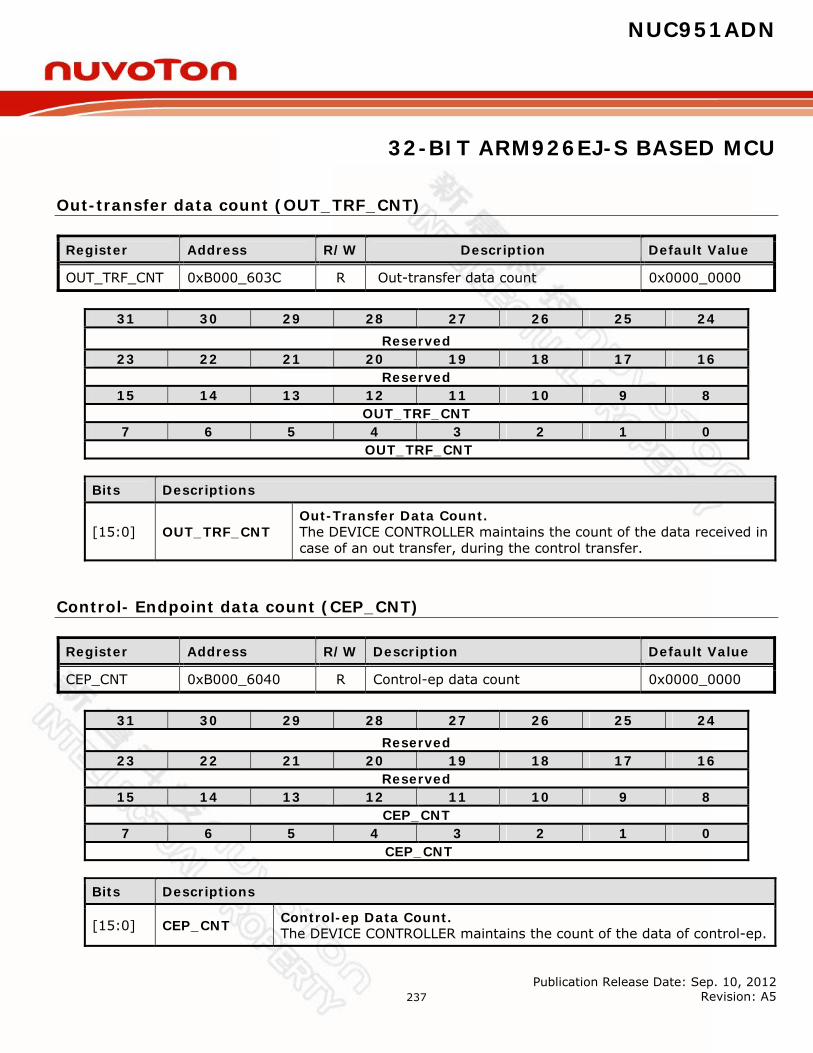
NUC951ADN
32-BIT ARM926EJ-S BASED MCU
Publication Release Date: Sep. 10, 2012 Revision: A5
237
Out-transfer data count (OUT_TRF_CNT)
Register Address R/W Description Default Value
OUT_TRF_CNT 0xB000_603C R Out-transfer data count 0x0000_0000
31 30 29 28 27 26 25 24
Reserved 23 22 21 20 19 18 17 16
Reserved 15 14 13 12 11 10 9 8
OUT_TRF_CNT 7 6 5 4 3 2 1 0
OUT_TRF_CNT
Bits Descriptions
[15:0] OUT_TRF_CNT Out-Transfer Data Count. The DEVICE CONTROLLER maintains the count of the data received in case of an out transfer, during the control transfer.
Control- Endpoint data count (CEP_CNT)
Register Address R/W Description Default Value
CEP_CNT 0xB000_6040 R Control-ep data count 0x0000_0000
31 30 29 28 27 26 25 24
Reserved 23 22 21 20 19 18 17 16
Reserved 15 14 13 12 11 10 9 8
CEP_CNT 7 6 5 4 3 2 1 0
CEP_CNT
Bits Descriptions
[15:0] CEP_CNT Control-ep Data Count. The DEVICE CONTROLLER maintains the count of the data of control-ep.
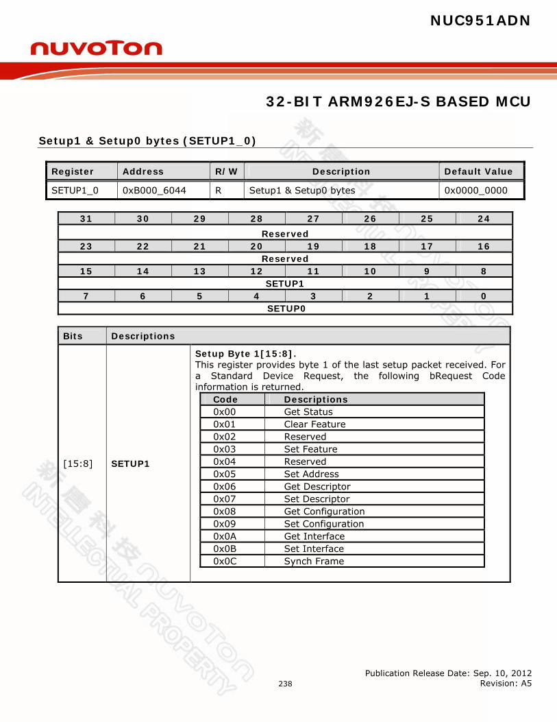
NUC951ADN
32-BIT ARM926EJ-S BASED MCU
Publication Release Date: Sep. 10, 2012 Revision: A5
238
Setup1 & Setup0 bytes (SETUP1_0)
Register Address R/W Description Default Value
SETUP1_0 0xB000_6044 R Setup1 & Setup0 bytes 0x0000_0000
31 30 29 28 27 26 25 24
Reserved 23 22 21 20 19 18 17 16
Reserved 15 14 13 12 11 10 9 8
SETUP1 7 6 5 4 3 2 1 0
SETUP0
Bits Descriptions
[15:8] SETUP1
Setup Byte 1[15:8]. This register provides byte 1 of the last setup packet received. For a Standard Device Request, the following bRequest Code information is returned.
Code Descriptions 0x00 Get Status 0x01 Clear Feature 0x02 Reserved 0x03 Set Feature 0x04 Reserved 0x05 Set Address 0x06 Get Descriptor 0x07 Set Descriptor 0x08 Get Configuration 0x09 Set Configuration 0x0A Get Interface 0x0B Set Interface 0x0C Synch Frame
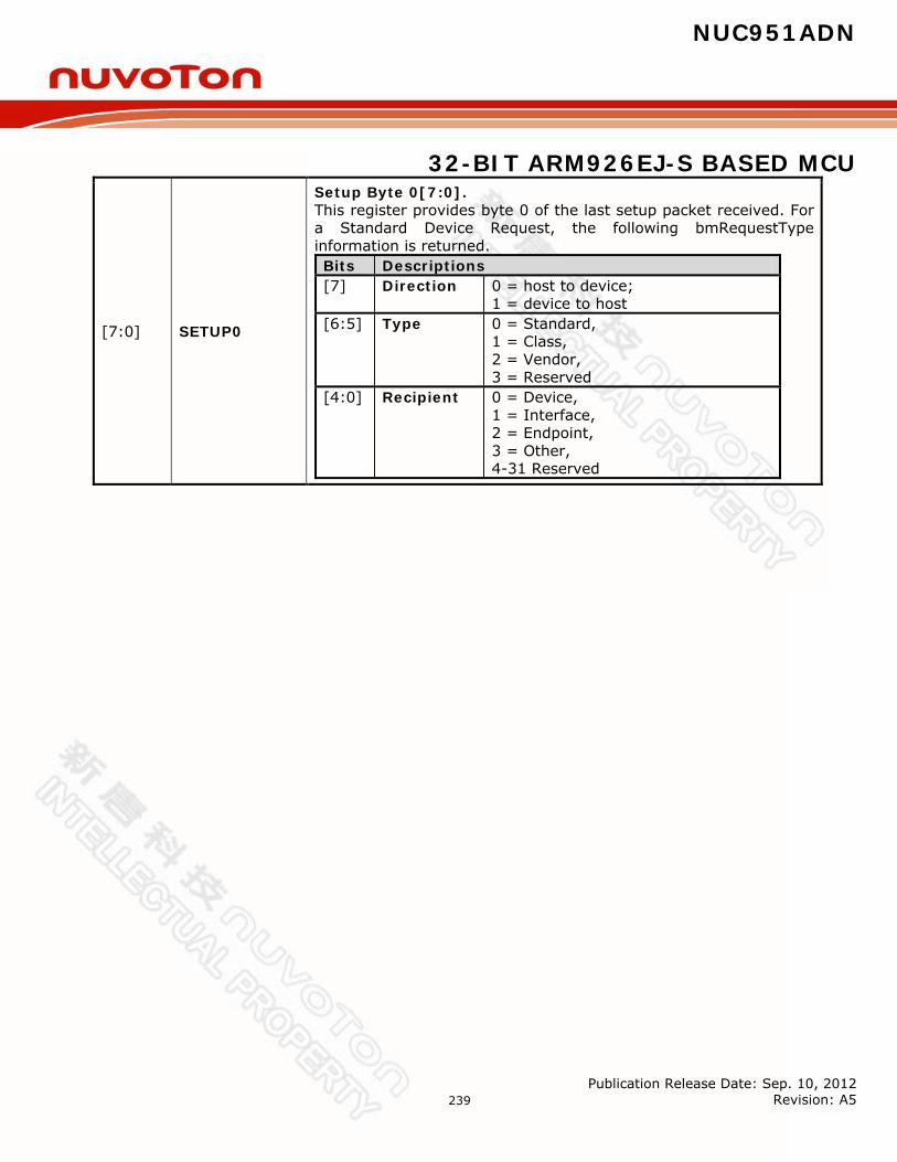
NUC951ADN
32-BIT ARM926EJ-S BASED MCU
Publication Release Date: Sep. 10, 2012 Revision: A5
239
[7:0] SETUP0
Setup Byte 0[7:0]. This register provides byte 0 of the last setup packet received. For a Standard Device Request, the following bmRequestType information is returned. Bits Descriptions [7] Direction 0 = host to device;
1 = device to host [6:5] Type 0 = Standard,
1 = Class, 2 = Vendor, 3 = Reserved
[4:0] Recipient 0 = Device, 1 = Interface, 2 = Endpoint, 3 = Other, 4-31 Reserved

NUC951ADN
32-BIT ARM926EJ-S BASED MCU
Publication Release Date: Sep. 10, 2012 Revision: A5
240
Setup3 & Setup2 bytes (SETUP3_2)
Register Address R/W Description Default Value
SETUP3_2 0xB000_6048 R Setup3 & Setup2 bytes 0x0000_0000
31 30 29 28 27 26 25 24
Reserved 23 22 21 20 19 18 17 16
Reserved 15 14 13 12 11 10 9 8
SETUP3 7 6 5 4 3 2 1 0
SETUP2
Bits Descriptions
[15:8] SETUP3
Setup Byte 3 [15:8]. This register provides byte 3 of the last setup packet received. For a Standard Device Request, the most significant byte of the wValue field is returned.
[7:0] SETUP2
Setup Byte 2 [7:0]. This register provides byte 2 of the last setup packet received. For a Standard Device Request, the least significant byte of the wValue field is returned.

NUC951ADN
32-BIT ARM926EJ-S BASED MCU
Publication Release Date: Sep. 10, 2012 Revision: A5
241
Setup5 & Setup4 bytes (SETUP5_4)
Register Address R/W Description Default Value
SETUP5_4 0xB000_604C R Setup5 & Setup4 bytes 0x0000_0000
31 30 29 28 27 26 25 24
Reserved 23 22 21 20 19 18 17 16
Reserved 15 14 13 12 11 10 9 8
SETUP5 7 6 5 4 3 2 1 0
SETUP4
Bits Descriptions
[15:8] SETUP5
Setup Byte 5[15:8]. This register provides byte 5 of the last setup packet received. For a Standard Device Request, the most significant byte of the wIndex field is returned.
[7:0] SETUP4
Setup Byte 4[7:0]. This register provides byte 4 of the last setup packet received. For a Standard Device Request, the least significant byte of the wIndex is returned.
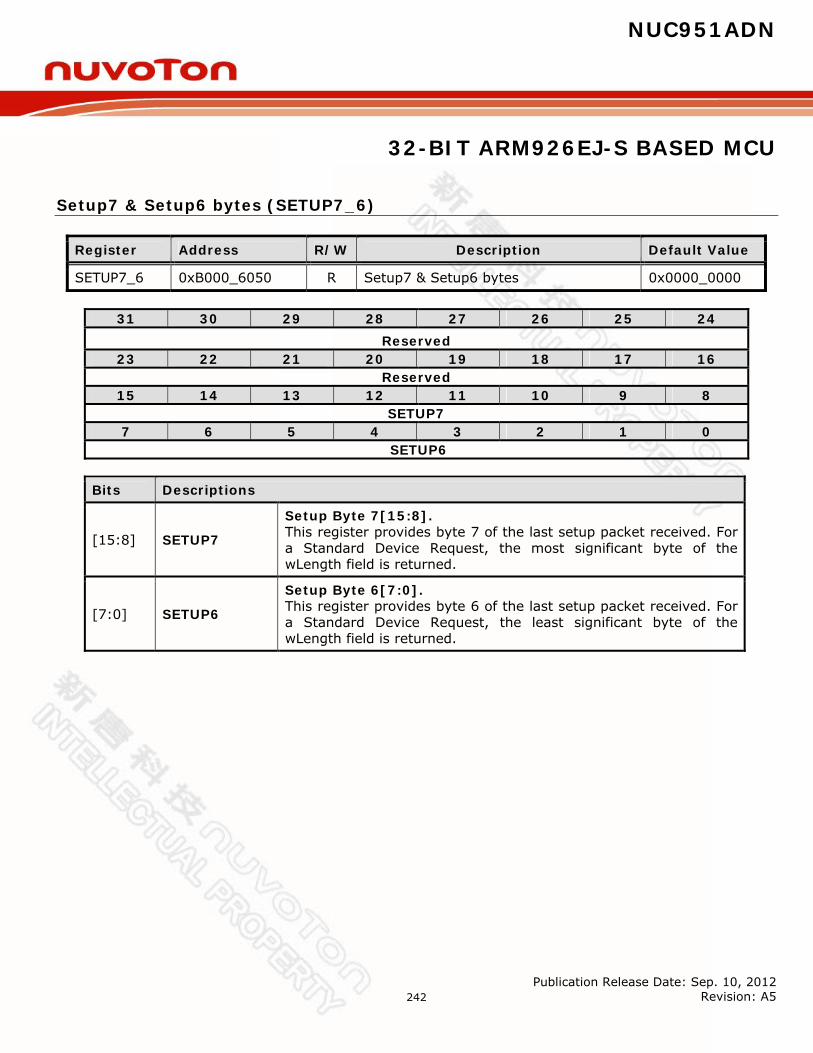
NUC951ADN
32-BIT ARM926EJ-S BASED MCU
Publication Release Date: Sep. 10, 2012 Revision: A5
242
Setup7 & Setup6 bytes (SETUP7_6)
Register Address R/W Description Default Value
SETUP7_6 0xB000_6050 R Setup7 & Setup6 bytes 0x0000_0000
31 30 29 28 27 26 25 24
Reserved 23 22 21 20 19 18 17 16
Reserved 15 14 13 12 11 10 9 8
SETUP7 7 6 5 4 3 2 1 0
SETUP6
Bits Descriptions
[15:8] SETUP7
Setup Byte 7[15:8]. This register provides byte 7 of the last setup packet received. For a Standard Device Request, the most significant byte of the wLength field is returned.
[7:0] SETUP6
Setup Byte 6[7:0]. This register provides byte 6 of the last setup packet received. For a Standard Device Request, the least significant byte of the wLength field is returned.

NUC951ADN
32-BIT ARM926EJ-S BASED MCU
Publication Release Date: Sep. 10, 2012 Revision: A5
243
Control Endpoint RAM Start Address Register (CEP_START_ADDR)
Register Address R/W Description Default Value
CEP_START_ADDR 0xB000_6054 R/W Control EP RAM Start Address Register 0x0000_0000
31 30 29 28 27 26 25 24
Reserved 23 22 21 20 19 18 17 16
Reserved 15 14 13 12 11 10 9 8
Reserved CEP_START_ADDR 7 6 5 4 3 2 1 0
CEP_START_ADDR
Bits Descriptions
[10:0] CEP_START_ADDR This is the start-address of the RAM space allocated for the control-endpoint

NUC951ADN
32-BIT ARM926EJ-S BASED MCU
Publication Release Date: Sep. 10, 2012 Revision: A5
244
Control Endpoint RAM End Address Register (CEP_END_ADDR)
Register Address R/W Description Default Value
CEP_END_ADDR 0xB000_6058 R/W Control EP RAM End Address Register 0x0000_0000
31 30 29 28 27 26 25 24
Reserved 23 22 21 20 19 18 17 16
Reserved 15 14 13 12 11 10 9 8
Reserved CEP_END_ADDR 7 6 5 4 3 2 1 0
CEP_END_ADDR
Bits Descriptions
[10:0] CEP_END_ADDR This is the end-address of the RAM space allocated for the control-endpoint

NUC951ADN
32-BIT ARM926EJ-S BASED MCU
Publication Release Date: Sep. 10, 2012 Revision: A5
245
DMA Control Status Register (DMA_CTRL_STS)
Register Address R/W Description Default Value
DMA_CTRL_STS 0xB000_605C R/W DMA Control Status Register 0x0000_0000
31 30 29 28 27 26 25 24
Reserved 23 22 21 20 19 18 17 16
Reserved 15 14 13 12 11 10 9 8
Reserved 7 6 5 4 3 2 1 0
RST_DMA SCAT_GA_EN DMA_EN DMA_RD DMA_ADDR
Bits Descriptions
[7] RST_DMA Reset DMA state machine.
[6] SCAT_GA_EN Scatter gather function enable
[5] DMA_EN DMA Enable Bit
[4] DMA_RD DMA Operation Bit. If ‘1’, the operation is a DMA read and if ‘0’ the operation is a DMA write.
[3:0] DMA_ADDR DMA ep_addr Bits When enable scatter gather DMA function, SCAT_GA_EN needs to be set high and DMA_CNT set to 8 bytes. Then DMA will enable to fetch the descriptor which describes the real memory address and length. The descriptor will be a 8-byte format, like the following:
[31] [30] [29:0] MEM_ADDR[31:0]
EOT RD reserved count[19:0] MEM_ADDR: It specifies the memory address (AHB address). EOT: end of transfer. When this bit sets to high, it means this is the last descriptor. RD: “1” means read from memory into buffer. “0” means read from buffer into memory.
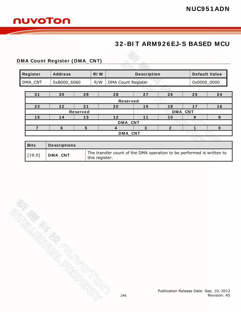
NUC951ADN
32-BIT ARM926EJ-S BASED MCU
Publication Release Date: Sep. 10, 2012 Revision: A5
246
DMA Count Register (DMA_CNT)
Register Address R/W Description Default Value
DMA_CNT 0xB000_6060 R/W DMA Count Register 0x0000_0000
31 30 29 28 27 26 25 24
Reserved 23 22 21 20 19 18 17 16
Reserved DMA_CNT 15 14 13 12 11 10 9 8
DMA_CNT 7 6 5 4 3 2 1 0
DMA_CNT
Bits Descriptions
[19:0] DMA_CNT The transfer count of the DMA operation to be performed is written to this register.

NUC951ADN
32-BIT ARM926EJ-S BASED MCU
Publication Release Date: Sep. 10, 2012 Revision: A5
247
Endpoint A~F Data Register (EPA_DATA_BUF~ EPF_DATA_BUF)
Register Address R/W Description Default Value
EPA_DATA_BUF 0xB000_6064 R/W Endpoint A Data Register 0x0000_0000
EPB_DATA_BUF 0xB000_608C R/W Endpoint B Data Register 0x0000_0000
EPC_DATA_BUF 0xB000_60B4 R/W Endpoint C Data Register 0x0000_0000
EPD_DATA_BUF 0xB000_60DC R/W Endpoint D Data Register 0x0000_0000
EPE_DATA_BUF 0xB000_6104 R/W Endpoint E Data Register 0x0000_0000
EPF_DATA_BUF 0xB000_612C R/W Endpoint F Data Register 0x0000_0000
31 30 29 28 27 26 25 24
Reserved 23 22 21 20 19 18 17 16
Reserved 15 14 13 12 11 10 9 8
EP_DATA_BUF 7 6 5 4 3 2 1 0
EP_DATA_BUF
Bits Descriptions
[15:0] EP_DATA_BUF
Endpoint A~F Data Register. Bits [15:8] of this register provide the high order byte and bits [7:0] of this register provide the lower order byte for the buffer transaction (read or write).
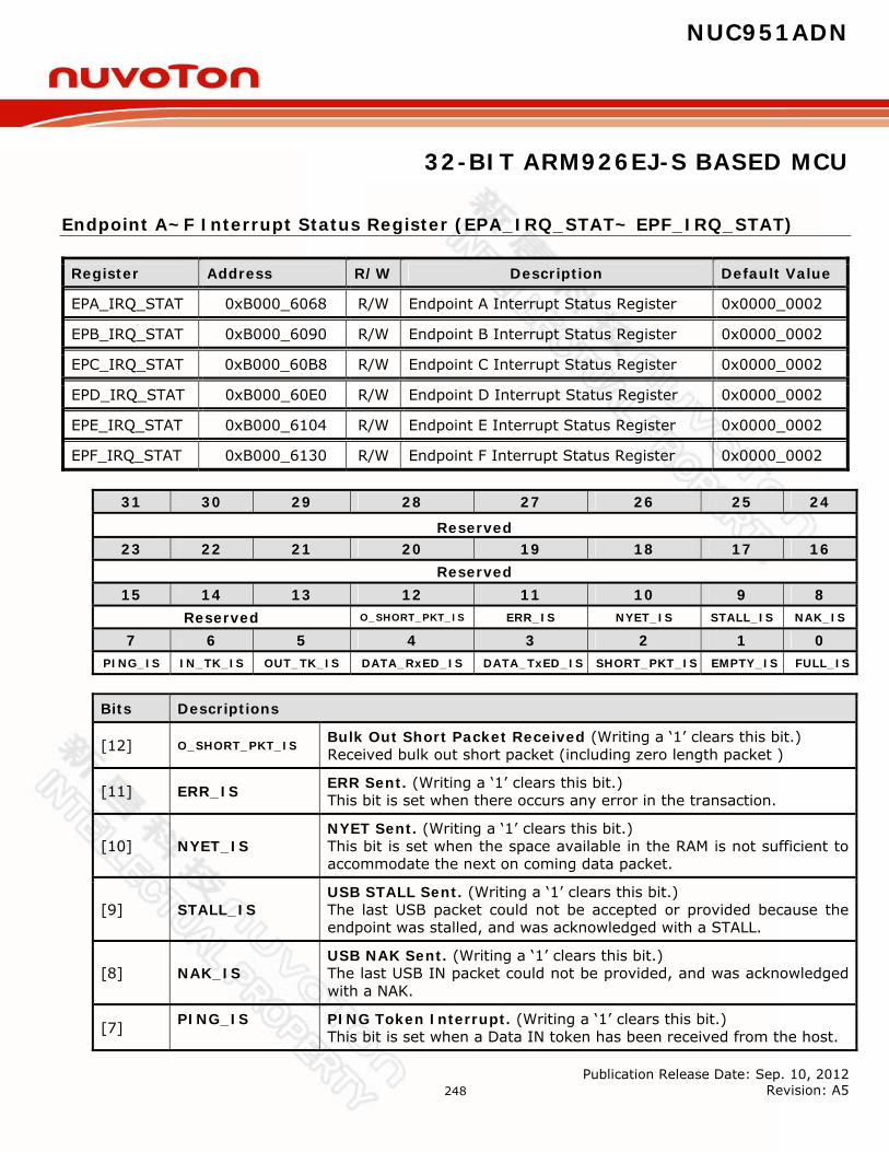
NUC951ADN
32-BIT ARM926EJ-S BASED MCU
Publication Release Date: Sep. 10, 2012 Revision: A5
248
Endpoint A~F Interrupt Status Register (EPA_IRQ_STAT~ EPF_IRQ_STAT)
Register Address R/W Description Default Value
EPA_IRQ_STAT 0xB000_6068 R/W Endpoint A Interrupt Status Register 0x0000_0002
EPB_IRQ_STAT 0xB000_6090 R/W Endpoint B Interrupt Status Register 0x0000_0002
EPC_IRQ_STAT 0xB000_60B8 R/W Endpoint C Interrupt Status Register 0x0000_0002
EPD_IRQ_STAT 0xB000_60E0 R/W Endpoint D Interrupt Status Register 0x0000_0002
EPE_IRQ_STAT 0xB000_6104 R/W Endpoint E Interrupt Status Register 0x0000_0002
EPF_IRQ_STAT 0xB000_6130 R/W Endpoint F Interrupt Status Register 0x0000_0002
31 30 29 28 27 26 25 24
Reserved 23 22 21 20 19 18 17 16
Reserved 15 14 13 12 11 10 9 8
Reserved O_SHORT_PKT_IS ERR_IS NYET_IS STALL_IS NAK_IS
7 6 5 4 3 2 1 0 PING_IS IN_TK_IS OUT_TK_IS DATA_RxED_IS DATA_TxED_IS SHORT_PKT_IS EMPTY_IS FULL_IS
Bits Descriptions
[12] O_SHORT_PKT_IS Bulk Out Short Packet Received (Writing a ‘1’ clears this bit.) Received bulk out short packet (including zero length packet )
[11] ERR_IS ERR Sent. (Writing a ‘1’ clears this bit.) This bit is set when there occurs any error in the transaction.
[10] NYET_IS NYET Sent. (Writing a ‘1’ clears this bit.) This bit is set when the space available in the RAM is not sufficient to accommodate the next on coming data packet.
[9] STALL_IS USB STALL Sent. (Writing a ‘1’ clears this bit.) The last USB packet could not be accepted or provided because the endpoint was stalled, and was acknowledged with a STALL.
[8] NAK_IS USB NAK Sent. (Writing a ‘1’ clears this bit.) The last USB IN packet could not be provided, and was acknowledged with a NAK.
[7] PING_IS PING Token Interrupt. (Writing a ‘1’ clears this bit.) This bit is set when a Data IN token has been received from the host.
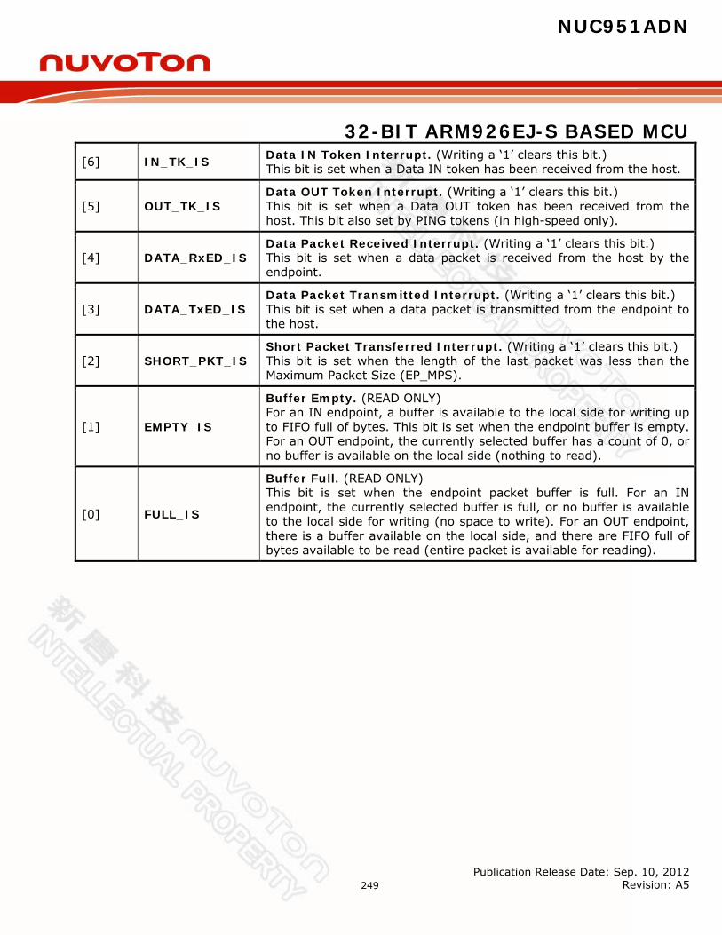
NUC951ADN
32-BIT ARM926EJ-S BASED MCU
Publication Release Date: Sep. 10, 2012 Revision: A5
249
[6] IN_TK_IS Data IN Token Interrupt. (Writing a ‘1’ clears this bit.) This bit is set when a Data IN token has been received from the host.
[5] OUT_TK_IS Data OUT Token Interrupt. (Writing a ‘1’ clears this bit.) This bit is set when a Data OUT token has been received from the host. This bit also set by PING tokens (in high-speed only).
[4] DATA_RxED_IS Data Packet Received Interrupt. (Writing a ‘1’ clears this bit.) This bit is set when a data packet is received from the host by the endpoint.
[3] DATA_TxED_IS Data Packet Transmitted Interrupt. (Writing a ‘1’ clears this bit.) This bit is set when a data packet is transmitted from the endpoint to the host.
[2] SHORT_PKT_IS Short Packet Transferred Interrupt. (Writing a ‘1’ clears this bit.) This bit is set when the length of the last packet was less than the Maximum Packet Size (EP_MPS).
[1] EMPTY_IS
Buffer Empty. (READ ONLY) For an IN endpoint, a buffer is available to the local side for writing up to FIFO full of bytes. This bit is set when the endpoint buffer is empty. For an OUT endpoint, the currently selected buffer has a count of 0, or no buffer is available on the local side (nothing to read).
[0] FULL_IS
Buffer Full. (READ ONLY) This bit is set when the endpoint packet buffer is full. For an IN endpoint, the currently selected buffer is full, or no buffer is available to the local side for writing (no space to write). For an OUT endpoint, there is a buffer available on the local side, and there are FIFO full of bytes available to be read (entire packet is available for reading).
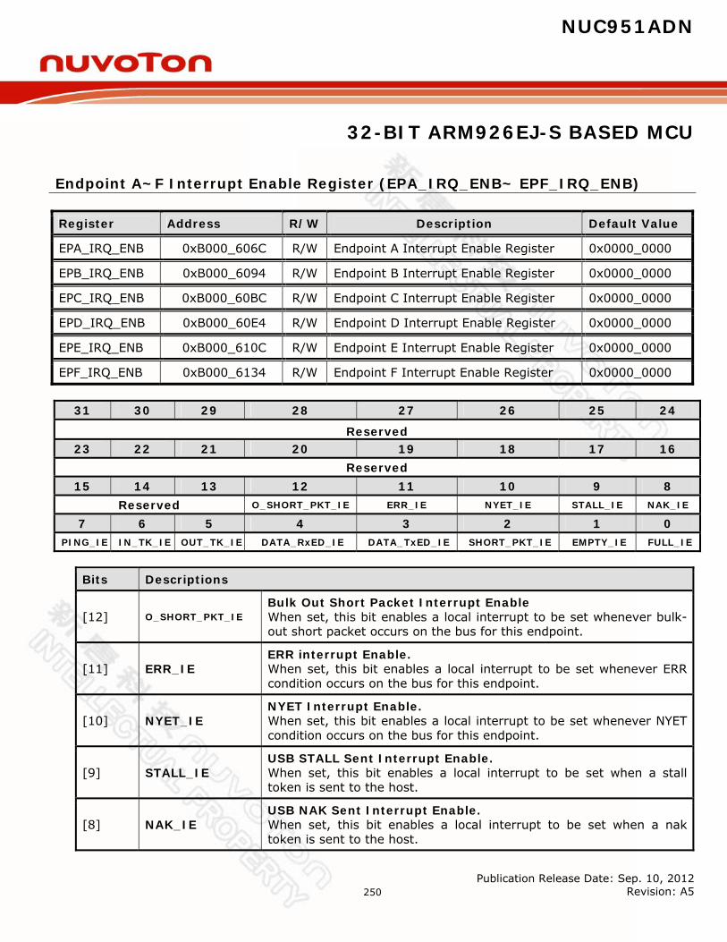
NUC951ADN
32-BIT ARM926EJ-S BASED MCU
Publication Release Date: Sep. 10, 2012 Revision: A5
250
Endpoint A~F Interrupt Enable Register (EPA_IRQ_ENB~ EPF_IRQ_ENB)
Register Address R/W Description Default Value
EPA_IRQ_ENB 0xB000_606C R/W Endpoint A Interrupt Enable Register 0x0000_0000
EPB_IRQ_ENB 0xB000_6094 R/W Endpoint B Interrupt Enable Register 0x0000_0000
EPC_IRQ_ENB 0xB000_60BC R/W Endpoint C Interrupt Enable Register 0x0000_0000
EPD_IRQ_ENB 0xB000_60E4 R/W Endpoint D Interrupt Enable Register 0x0000_0000
EPE_IRQ_ENB 0xB000_610C R/W Endpoint E Interrupt Enable Register 0x0000_0000
EPF_IRQ_ENB 0xB000_6134 R/W Endpoint F Interrupt Enable Register 0x0000_0000
31 30 29 28 27 26 25 24
Reserved 23 22 21 20 19 18 17 16
Reserved 15 14 13 12 11 10 9 8
Reserved O_SHORT_PKT_IE ERR_IE NYET_IE STALL_IE NAK_IE
7 6 5 4 3 2 1 0 PING_IE IN_TK_IE OUT_TK_IE DATA_RxED_IE DATA_TxED_IE SHORT_PKT_IE EMPTY_IE FULL_IE
Bits Descriptions
[12] O_SHORT_PKT_IE Bulk Out Short Packet Interrupt Enable When set, this bit enables a local interrupt to be set whenever bulk-out short packet occurs on the bus for this endpoint.
[11] ERR_IE ERR interrupt Enable. When set, this bit enables a local interrupt to be set whenever ERR condition occurs on the bus for this endpoint.
[10] NYET_IE NYET Interrupt Enable. When set, this bit enables a local interrupt to be set whenever NYET condition occurs on the bus for this endpoint.
[9] STALL_IE USB STALL Sent Interrupt Enable. When set, this bit enables a local interrupt to be set when a stall token is sent to the host.
[8] NAK_IE USB NAK Sent Interrupt Enable. When set, this bit enables a local interrupt to be set when a nak token is sent to the host.
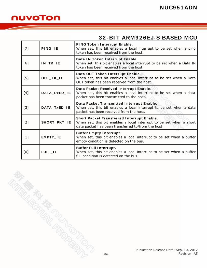
NUC951ADN
32-BIT ARM926EJ-S BASED MCU
Publication Release Date: Sep. 10, 2012 Revision: A5
251
[7] PING_IE PING Token Interrupt Enable. When set, this bit enables a local interrupt to be set when a ping token has been received from the host.
[6] IN_TK_IE Data IN Token Interrupt Enable. When set, this bit enables a local interrupt to be set when a Data IN token has been received from the host.
[5] OUT_TK_IE Data OUT Token Interrupt Enable. When set, this bit enables a local interrupt to be set when a Data OUT token has been received from the host.
[4] DATA_RxED_IE Data Packet Received Interrupt Enable. When set, this bit enables a local interrupt to be set when a data packet has been transmitted to the host.
[3] DATA_TxED_IE Data Packet Transmitted Interrupt Enable. When set, this bit enables a local interrupt to be set when a data packet has been received from the host.
[2] SHORT_PKT_IE Short Packet Transferred Interrupt Enable. When set, this bit enables a local interrupt to be set when a short data packet has been transferred to/from the host.
[1] EMPTY_IE Buffer Empty Interrupt. When set, this bit enables a local interrupt to be set when a buffer empty condition is detected on the bus.
[0] FULL_IE Buffer Full Interrupt. When set, this bit enables a local interrupt to be set when a buffer full condition is detected on the bus.
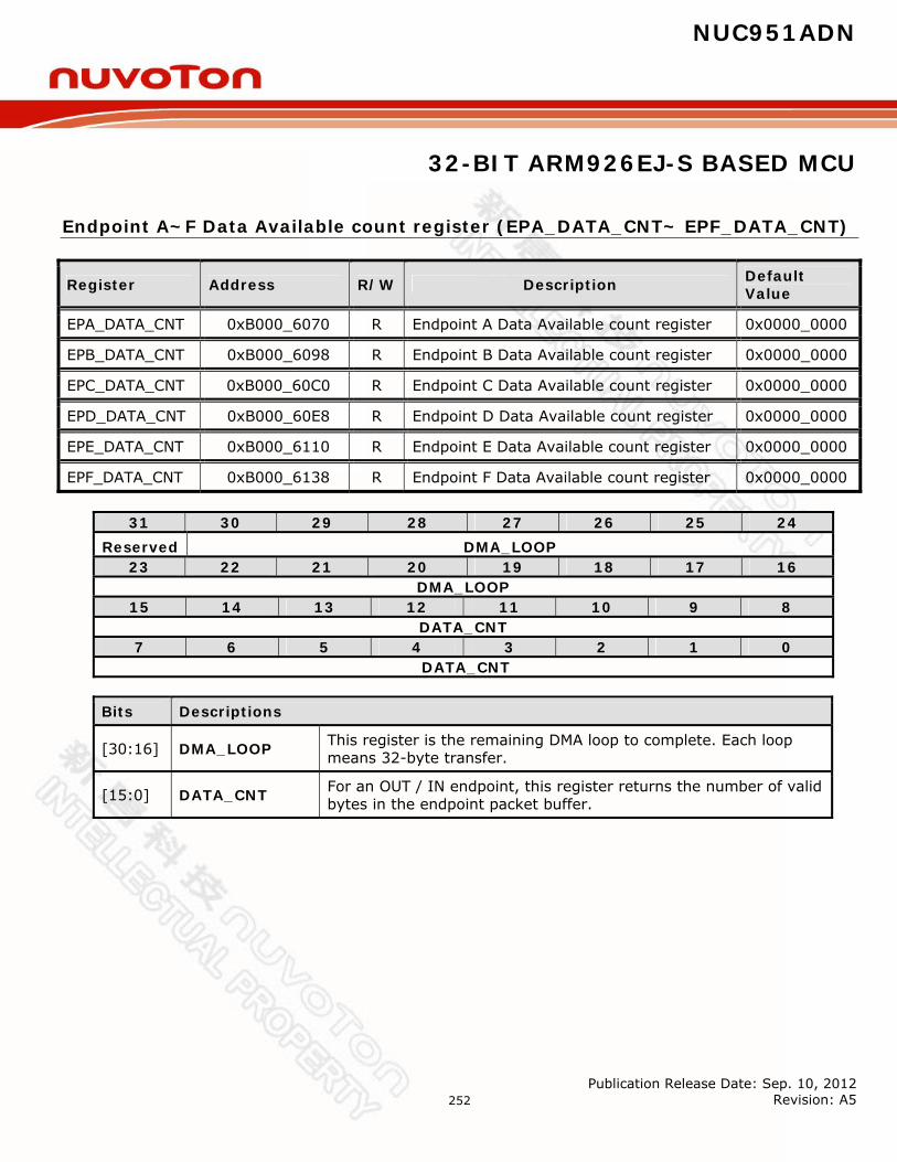
NUC951ADN
32-BIT ARM926EJ-S BASED MCU
Publication Release Date: Sep. 10, 2012 Revision: A5
252
Endpoint A~F Data Available count register (EPA_DATA_CNT~ EPF_DATA_CNT)
Register Address R/W Description Default Value
EPA_DATA_CNT 0xB000_6070 R Endpoint A Data Available count register 0x0000_0000
EPB_DATA_CNT 0xB000_6098 R Endpoint B Data Available count register 0x0000_0000
EPC_DATA_CNT 0xB000_60C0 R Endpoint C Data Available count register 0x0000_0000
EPD_DATA_CNT 0xB000_60E8 R Endpoint D Data Available count register 0x0000_0000
EPE_DATA_CNT 0xB000_6110 R Endpoint E Data Available count register 0x0000_0000
EPF_DATA_CNT 0xB000_6138 R Endpoint F Data Available count register 0x0000_0000
31 30 29 28 27 26 25 24
Reserved DMA_LOOP 23 22 21 20 19 18 17 16
DMA_LOOP 15 14 13 12 11 10 9 8
DATA_CNT 7 6 5 4 3 2 1 0
DATA_CNT
Bits Descriptions
[30:16] DMA_LOOP This register is the remaining DMA loop to complete. Each loop means 32-byte transfer.
[15:0] DATA_CNT For an OUT / IN endpoint, this register returns the number of valid bytes in the endpoint packet buffer.
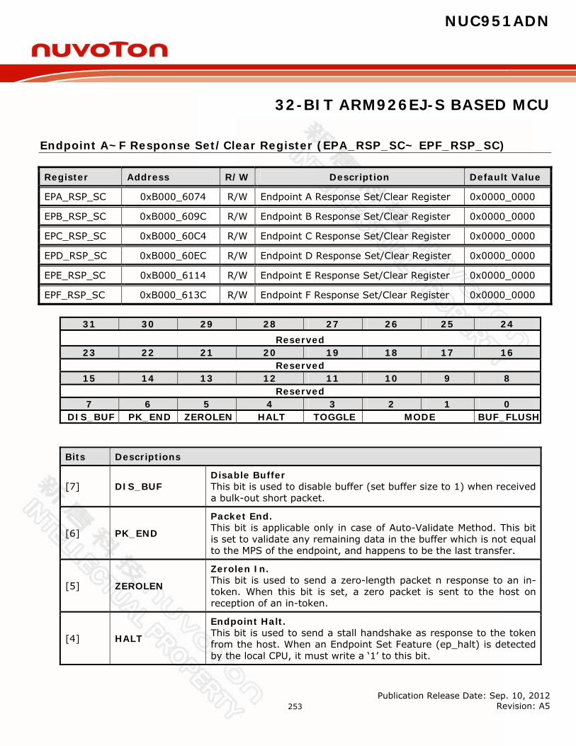
NUC951ADN
32-BIT ARM926EJ-S BASED MCU
Publication Release Date: Sep. 10, 2012 Revision: A5
253
Endpoint A~F Response Set/Clear Register (EPA_RSP_SC~ EPF_RSP_SC)
Register Address R/W Description Default Value
EPA_RSP_SC 0xB000_6074 R/W Endpoint A Response Set/Clear Register 0x0000_0000
EPB_RSP_SC 0xB000_609C R/W Endpoint B Response Set/Clear Register 0x0000_0000
EPC_RSP_SC 0xB000_60C4 R/W Endpoint C Response Set/Clear Register 0x0000_0000
EPD_RSP_SC 0xB000_60EC R/W Endpoint D Response Set/Clear Register 0x0000_0000
EPE_RSP_SC 0xB000_6114 R/W Endpoint E Response Set/Clear Register 0x0000_0000
EPF_RSP_SC 0xB000_613C R/W Endpoint F Response Set/Clear Register 0x0000_0000
31 30 29 28 27 26 25 24
Reserved 23 22 21 20 19 18 17 16
Reserved 15 14 13 12 11 10 9 8
Reserved 7 6 5 4 3 2 1 0
DIS_BUF PK_END ZEROLEN HALT TOGGLE MODE BUF_FLUSH
Bits Descriptions
[7] DIS_BUF Disable Buffer This bit is used to disable buffer (set buffer size to 1) when received a bulk-out short packet.
[6] PK_END
Packet End. This bit is applicable only in case of Auto-Validate Method. This bit is set to validate any remaining data in the buffer which is not equal to the MPS of the endpoint, and happens to be the last transfer.
[5] ZEROLEN
Zerolen In. This bit is used to send a zero-length packet n response to an in-token. When this bit is set, a zero packet is sent to the host on reception of an in-token.
[4] HALT
Endpoint Halt. This bit is used to send a stall handshake as response to the token from the host. When an Endpoint Set Feature (ep_halt) is detected by the local CPU, it must write a ‘1’ to this bit.
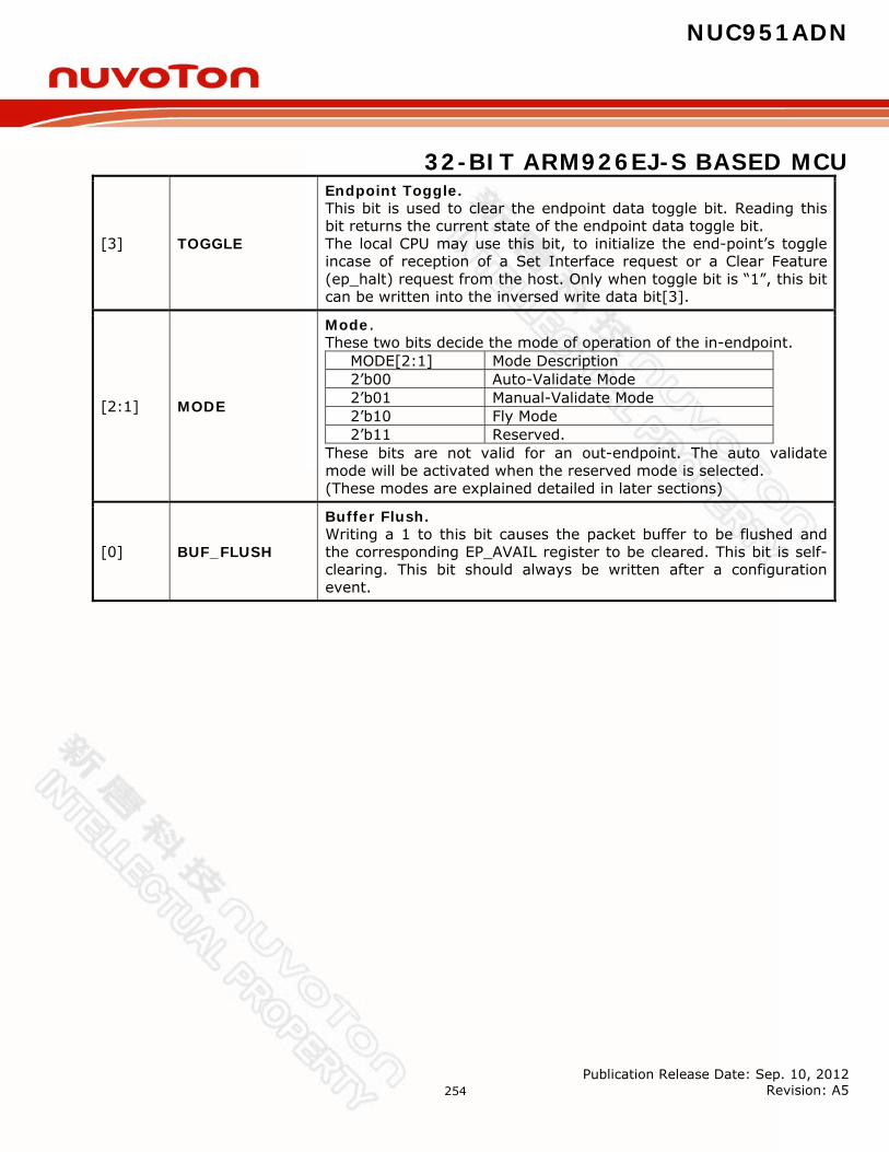
NUC951ADN
32-BIT ARM926EJ-S BASED MCU
Publication Release Date: Sep. 10, 2012 Revision: A5
254
[3] TOGGLE
Endpoint Toggle. This bit is used to clear the endpoint data toggle bit. Reading this bit returns the current state of the endpoint data toggle bit. The local CPU may use this bit, to initialize the end-point’s toggle incase of reception of a Set Interface request or a Clear Feature (ep_halt) request from the host. Only when toggle bit is “1”, this bit can be written into the inversed write data bit[3].
[2:1] MODE
Mode. These two bits decide the mode of operation of the in-endpoint.
MODE[2:1] Mode Description 2’b00 Auto-Validate Mode 2’b01 Manual-Validate Mode 2’b10 Fly Mode 2’b11 Reserved.
These bits are not valid for an out-endpoint. The auto validate mode will be activated when the reserved mode is selected. (These modes are explained detailed in later sections)
[0] BUF_FLUSH
Buffer Flush. Writing a 1 to this bit causes the packet buffer to be flushed and the corresponding EP_AVAIL register to be cleared. This bit is self-clearing. This bit should always be written after a configuration event.
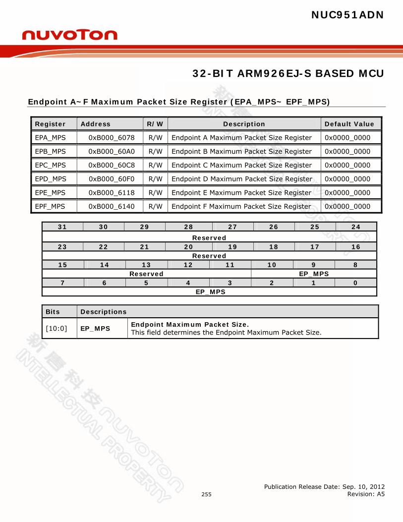
NUC951ADN
32-BIT ARM926EJ-S BASED MCU
Publication Release Date: Sep. 10, 2012 Revision: A5
255
Endpoint A~F Maximum Packet Size Register (EPA_MPS~ EPF_MPS)
Register Address R/W Description Default Value
EPA_MPS 0xB000_6078 R/W Endpoint A Maximum Packet Size Register 0x0000_0000
EPB_MPS 0xB000_60A0 R/W Endpoint B Maximum Packet Size Register 0x0000_0000
EPC_MPS 0xB000_60C8 R/W Endpoint C Maximum Packet Size Register 0x0000_0000
EPD_MPS 0xB000_60F0 R/W Endpoint D Maximum Packet Size Register 0x0000_0000
EPE_MPS 0xB000_6118 R/W Endpoint E Maximum Packet Size Register 0x0000_0000
EPF_MPS 0xB000_6140 R/W Endpoint F Maximum Packet Size Register 0x0000_0000
31 30 29 28 27 26 25 24
Reserved 23 22 21 20 19 18 17 16
Reserved 15 14 13 12 11 10 9 8
Reserved EP_MPS 7 6 5 4 3 2 1 0
EP_MPS
Bits Descriptions
[10:0] EP_MPS Endpoint Maximum Packet Size. This field determines the Endpoint Maximum Packet Size.

NUC951ADN
32-BIT ARM926EJ-S BASED MCU
Publication Release Date: Sep. 10, 2012 Revision: A5
256
Endpoint A~F Transfer Count Register (EPA_TRF_CNT~ EPF_TRF_CNT)
Register Address R/W Description Default Value
EPA_TRF_CNT 0xB000_607C R/W Endpoint A Transfer Count Register 0x0000_0000
EPB_TRF_CNT 0xB000_60A4 R/W Endpoint B Transfer Count Register 0x0000_0000
EPC_TRF_CNT 0xB000_60CC R/W Endpoint C Transfer Count Register 0x0000_0000
EPD_TRF_CNT 0xB000_60F4 R/W Endpoint D Transfer Count Register 0x0000_0000
EPE_TRF_CNT 0xB000_611C R/W Endpoint E Transfer Count Register 0x0000_0000
EPF_TRF_CNT 0xB000_6144 R/W Endpoint F Transfer Count Register 0x0000_0000
31 30 29 28 27 26 25 24
Reserved 23 22 21 20 19 18 17 16
Reserved 15 14 13 12 11 10 9 8
EP_TRF_CNT 7 6 5 4 3 2 1 0
EP_TRF_CNT
Bits Descriptions
[10:0] EP_TRF_CNT For IN endpoints, this field determines the total number of bytes to be sent to the host in case of manual validation method. For OUT endpoints, this field has no effect

NUC951ADN
32-BIT ARM926EJ-S BASED MCU
Publication Release Date: Sep. 10, 2012 Revision: A5
257
Endpoint A~F Configuration Register (EPA_CFG~ EPF_CFG)
Register Address R/W Description Default Value
EPA_CFG 0xB000_6080 R/W Endpoint A Configuration Register 0x0000_0012
EPB_CFG 0xB000_60A8 R/W Endpoint B Configuration Register 0x0000_0022
EPC_CFG 0xB000_60D0 R/W Endpoint C Configuration Register 0x0000_0032
EPD_CFG 0xB000_60F8 R/W Endpoint D Configuration Register 0x0000_0042
EPE_CFG 0xB000_6120 R/W Endpoint E Configuration Register 0x0000_0052
EPF_CFG 0xB000_6148 R/W Endpoint F Configuration Register 0x0000_0062
31 30 29 28 27 26 25 24
Reserved 23 22 21 20 19 18 17 16
Reserved 15 14 13 12 11 10 9 8
Reserved EP_MULT 7 6 5 4 3 2 1 0
EP_NUM EP_DIR EP_TYPE EP_VALID
Bits Descriptions
[9:8] EP_MULT
MULT Field. This field indicates number of transactions to be carried out in one single micro frame.
[9:8] Description 0x00 One transaction 0x01 Reserved 0x10 Reserved 0x11 Invalid
[7:4] EP_NUM Endpoint Number. This field selects the number of the endpoint. Valid numbers 1 to 15.
[3] EP_DIR
Endpoint Direction. EP_DIR = 0 - OUT EP (Host OUT to Device) EP_DIR = 1- IN EP (Host IN to Device) Note that a maximum of one OUT and IN endpoint is allowed for each endpoint number.
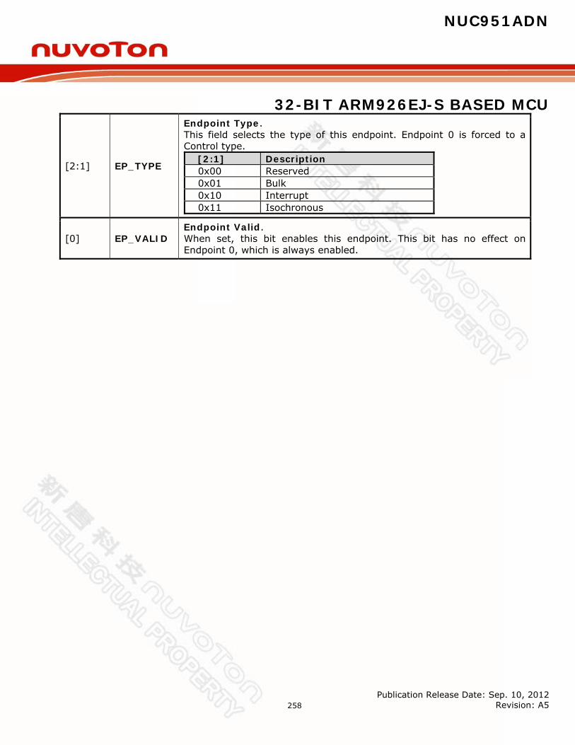
NUC951ADN
32-BIT ARM926EJ-S BASED MCU
Publication Release Date: Sep. 10, 2012 Revision: A5
258
[2:1] EP_TYPE
Endpoint Type. This field selects the type of this endpoint. Endpoint 0 is forced to a Control type.
[2:1] Description 0x00 Reserved 0x01 Bulk 0x10 Interrupt 0x11 Isochronous
[0] EP_VALID Endpoint Valid. When set, this bit enables this endpoint. This bit has no effect on Endpoint 0, which is always enabled.
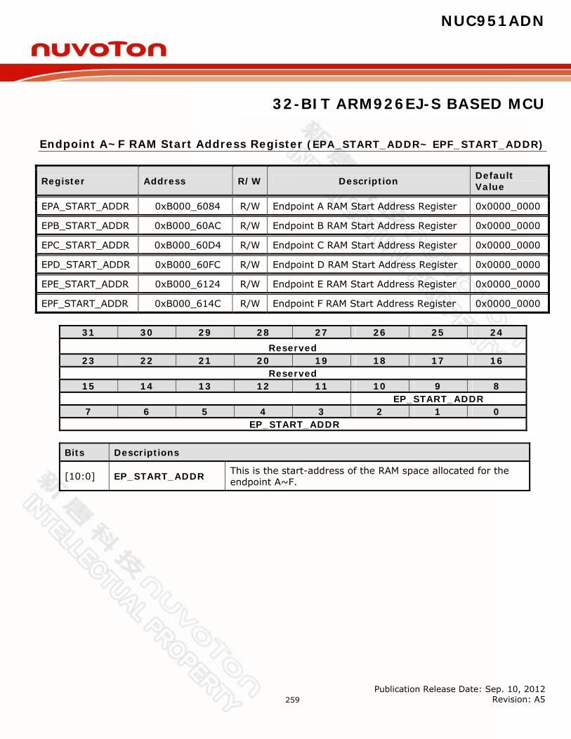
NUC951ADN
32-BIT ARM926EJ-S BASED MCU
Publication Release Date: Sep. 10, 2012 Revision: A5
259
Endpoint A~F RAM Start Address Register (EPA_START_ADDR~ EPF_START_ADDR)
Register Address R/W Description Default Value
EPA_START_ADDR 0xB000_6084 R/W Endpoint A RAM Start Address Register 0x0000_0000
EPB_START_ADDR 0xB000_60AC R/W Endpoint B RAM Start Address Register 0x0000_0000
EPC_START_ADDR 0xB000_60D4 R/W Endpoint C RAM Start Address Register 0x0000_0000
EPD_START_ADDR 0xB000_60FC R/W Endpoint D RAM Start Address Register 0x0000_0000
EPE_START_ADDR 0xB000_6124 R/W Endpoint E RAM Start Address Register 0x0000_0000
EPF_START_ADDR 0xB000_614C R/W Endpoint F RAM Start Address Register 0x0000_0000
31 30 29 28 27 26 25 24
Reserved 23 22 21 20 19 18 17 16
Reserved 15 14 13 12 11 10 9 8
EP_START_ADDR 7 6 5 4 3 2 1 0
EP_START_ADDR
Bits Descriptions
[10:0] EP_START_ADDR This is the start-address of the RAM space allocated for the endpoint A~F.
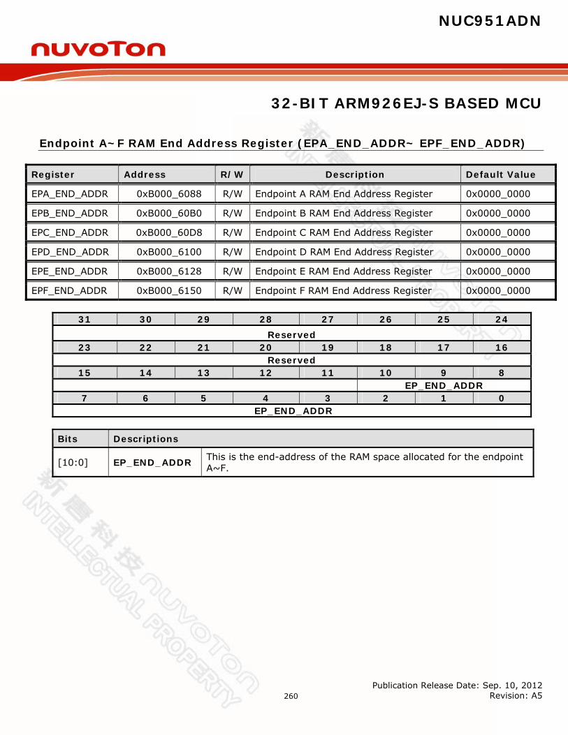
NUC951ADN
32-BIT ARM926EJ-S BASED MCU
Publication Release Date: Sep. 10, 2012 Revision: A5
260
Endpoint A~F RAM End Address Register (EPA_END_ADDR~ EPF_END_ADDR)
Register Address R/W Description Default Value
EPA_END_ADDR 0xB000_6088 R/W Endpoint A RAM End Address Register 0x0000_0000
EPB_END_ADDR 0xB000_60B0 R/W Endpoint B RAM End Address Register 0x0000_0000
EPC_END_ADDR 0xB000_60D8 R/W Endpoint C RAM End Address Register 0x0000_0000
EPD_END_ADDR 0xB000_6100 R/W Endpoint D RAM End Address Register 0x0000_0000
EPE_END_ADDR 0xB000_6128 R/W Endpoint E RAM End Address Register 0x0000_0000
EPF_END_ADDR 0xB000_6150 R/W Endpoint F RAM End Address Register 0x0000_0000
31 30 29 28 27 26 25 24
Reserved 23 22 21 20 19 18 17 16
Reserved 15 14 13 12 11 10 9 8
EP_END_ADDR 7 6 5 4 3 2 1 0
EP_END_ADDR
Bits Descriptions
[10:0] EP_END_ADDR This is the end-address of the RAM space allocated for the endpoint A~F.
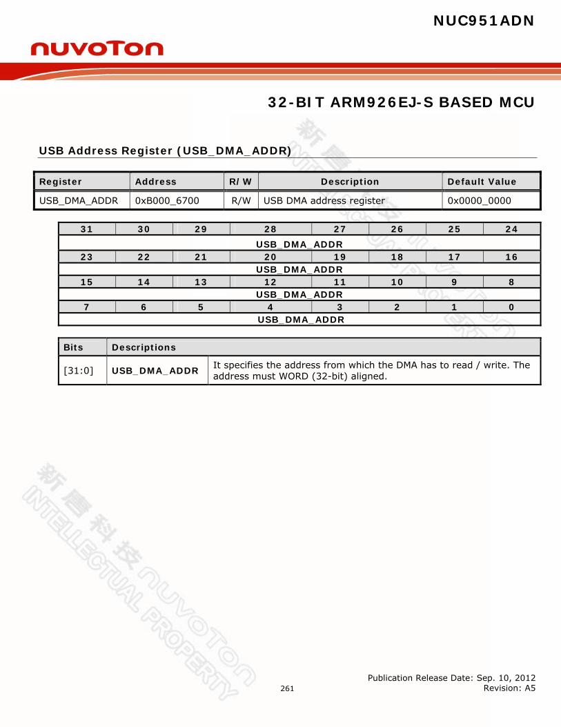
NUC951ADN
32-BIT ARM926EJ-S BASED MCU
Publication Release Date: Sep. 10, 2012 Revision: A5
261
USB Address Register (USB_DMA_ADDR)
Register Address R/W Description Default Value
USB_DMA_ADDR 0xB000_6700 R/W USB DMA address register 0x0000_0000
31 30 29 28 27 26 25 24
USB_DMA_ADDR 23 22 21 20 19 18 17 16
USB_DMA_ADDR 15 14 13 12 11 10 9 8
USB_DMA_ADDR 7 6 5 4 3 2 1 0
USB_DMA_ADDR
Bits Descriptions
[31:0] USB_DMA_ADDR It specifies the address from which the DMA has to read / write. The address must WORD (32-bit) aligned.
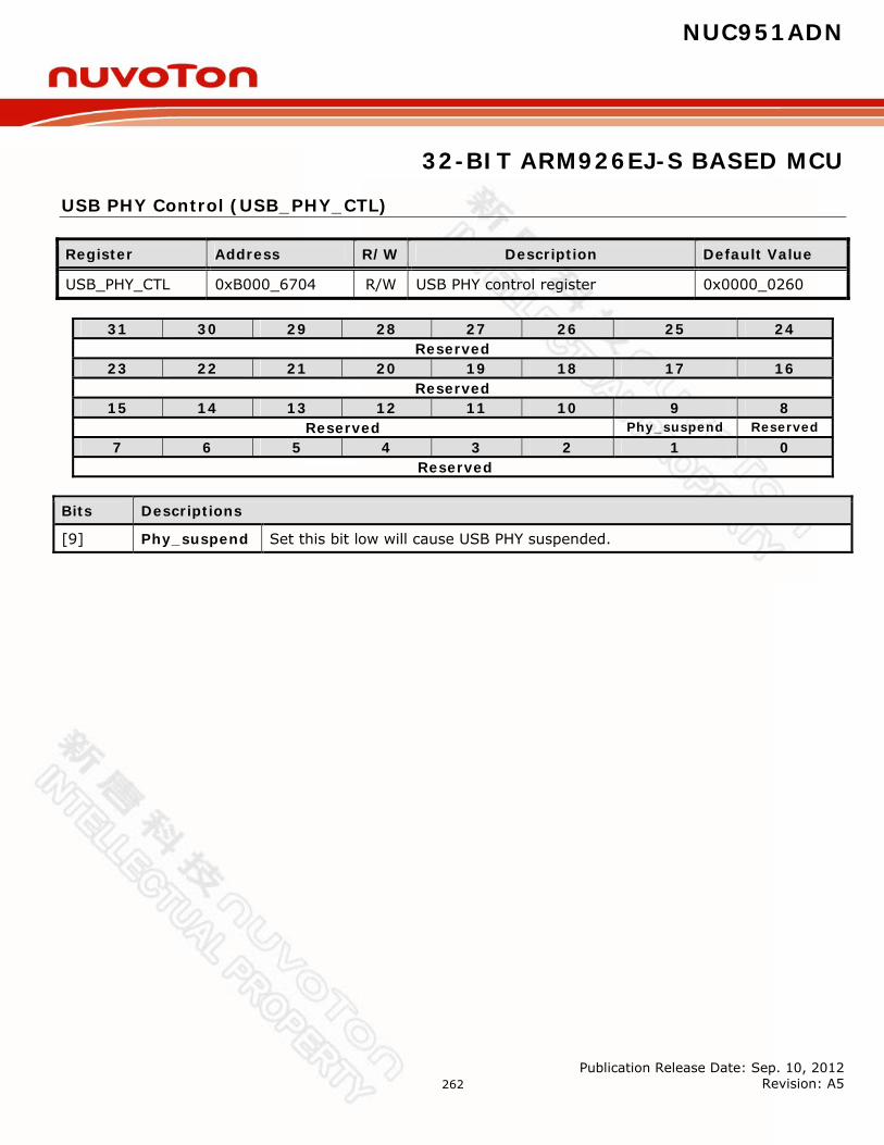
NUC951ADN
32-BIT ARM926EJ-S BASED MCU
Publication Release Date: Sep. 10, 2012 Revision: A5
262
USB PHY Control (USB_PHY_CTL)
Register Address R/W Description Default Value
USB_PHY_CTL 0xB000_6704 R/W USB PHY control register 0x0000_0260
31 30 29 28 27 26 25 24
Reserved 23 22 21 20 19 18 17 16
Reserved 15 14 13 12 11 10 9 8
Reserved Phy_suspend Reserved 7 6 5 4 3 2 1 0
Reserved Bits Descriptions
[9] Phy_suspend Set this bit low will cause USB PHY suspended.

NUC951ADN
32-BIT ARM926EJ-S BASED MCU
Publication Release Date: Sep. 10, 2012 Revision: A5
263
7.9 DMA Controller (DMAC) The DMA Controller provides a DMA (Direct Memory Access) function for ATAPI and FMI to exchange data between system memory (ex. SDRAM) and shared buffer (one 2048 bytes). Arbitration of DMA request between ATAPI and FMI is done by DMAC’s bus master (Priority: ATAPI > FMI). Software just simply fills in the starting address and enables DMAC, and then you can let DMAC to handle the data transfer automatically. There is one 2048 bytes shared buffer inside DMAC, separate into four 512 bytes ping-pong FIFO. It can provide multi-block transfers using ping-pong mechanism for ATAPI and FMI. Software can access these shared buffers directly when ATAPI and FMI are not in busy. Features:
Support single DMA channel Support hardware Scatter-Getter function One 2048 bytes shared buffer is embedded Automatic arbitration of DMA request for ATAPI and FMI
7.9.1 DMA Controller Registers Map R: read only, W: write only, R/W: both read and write Register Offset R/W Description Reset Value
Shared Buffer FB_0 …… FB_511
0XB000_C000 ……
0xB000_C7FC R/W Shared Buffer (FIFO) N/A
DMAC Registers
DMACCSR 0xB000_C800 R/W DMAC Control and Status Register 0x0000_0000
DMACSAR1 0xB000_C804 R/W DMAC Transfer Starting Address Register 1 0x0000_0000
DMACSAR2 0xB000_C808 R/W DMAC Transfer Starting Address Register 2 0x0000_0000
DMACBCR 0xB000_C80C R DMAC Transfer Byte Count Register 0x0000_0000
DMACIER 0xB000_C810 R/W DMAC Interrupt Enable Register 0x0000_0001
DMACISR 0xB000_C814 R/W DMAC Interrupt Status Register 0x0000_0000
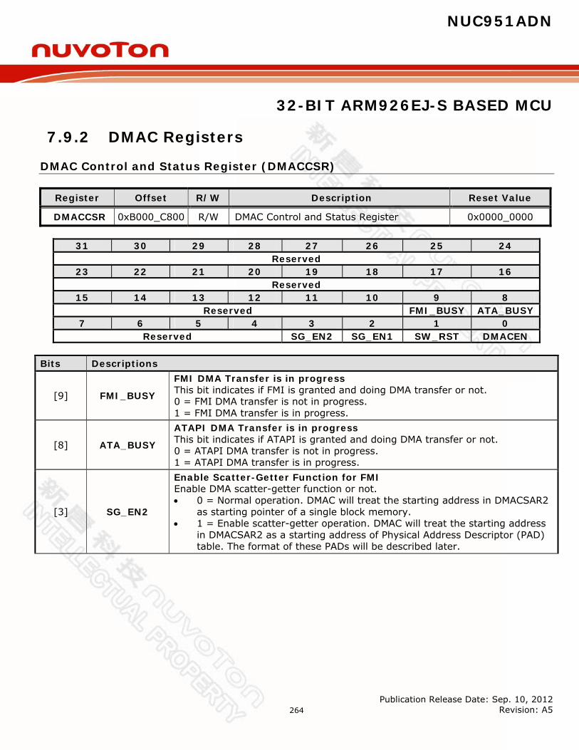
NUC951ADN
32-BIT ARM926EJ-S BASED MCU
Publication Release Date: Sep. 10, 2012 Revision: A5
264
7.9.2 DMAC Registers
DMAC Control and Status Register (DMACCSR)
Register Offset R/W Description Reset Value
DMACCSR 0xB000_C800 R/W DMAC Control and Status Register 0x0000_0000
31 30 29 28 27 26 25 24 Reserved
23 22 21 20 19 18 17 16 Reserved
15 14 13 12 11 10 9 8 Reserved FMI_BUSY ATA_BUSY
7 6 5 4 3 2 1 0 Reserved SG_EN2 SG_EN1 SW_RST DMACEN
Bits Descriptions
[9] FMI_BUSY
FMI DMA Transfer is in progress This bit indicates if FMI is granted and doing DMA transfer or not. 0 = FMI DMA transfer is not in progress. 1 = FMI DMA transfer is in progress.
[8] ATA_BUSY
ATAPI DMA Transfer is in progress This bit indicates if ATAPI is granted and doing DMA transfer or not. 0 = ATAPI DMA transfer is not in progress. 1 = ATAPI DMA transfer is in progress.
[3] SG_EN2
Enable Scatter-Getter Function for FMI Enable DMA scatter-getter function or not. 0 = Normal operation. DMAC will treat the starting address in DMACSAR2
as starting pointer of a single block memory. 1 = Enable scatter-getter operation. DMAC will treat the starting address
in DMACSAR2 as a starting address of Physical Address Descriptor (PAD) table. The format of these PADs will be described later.
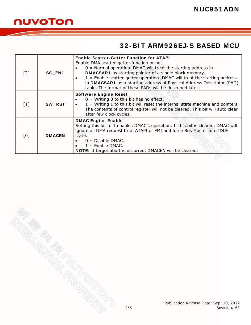
NUC951ADN
32-BIT ARM926EJ-S BASED MCU
Publication Release Date: Sep. 10, 2012 Revision: A5
265
[2] SG_EN1
Enable Scatter-Getter Function for ATAPI Enable DMA scatter-getter function or not. 0 = Normal operation. DMAC will treat the starting address in
DMACSAR1 as starting pointer of a single block memory. 1 = Enable scatter-getter operation. DMAC will treat the starting address
in DMACSAR1 as a starting address of Physical Address Descriptor (PAD) table. The format of these PADs will be described later.
[1] SW_RST
Software Engine Reset 0 = Writing 0 to this bit has no effect. 1 = Writing 1 to this bit will reset the internal state machine and pointers.
The contents of control register will not be cleared. This bit will auto clear after few clock cycles.
[0] DMACEN
DMAC Engine Enable Setting this bit to 1 enables DMAC’s operation. If this bit is cleared, DMAC will ignore all DMA request from ATAPI or FMI and force Bus Master into IDLE state. 0 = Disable DMAC. 1 = Enable DMAC. NOTE: If target abort is occurred, DMACEN will be cleared.
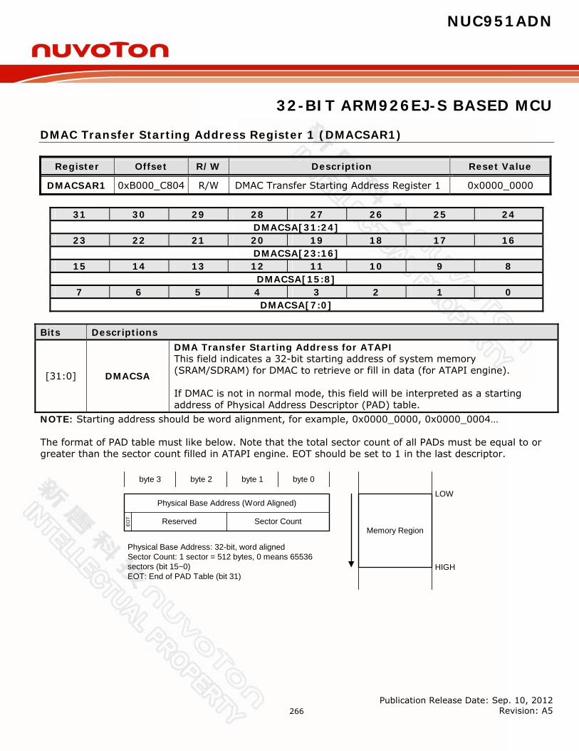
NUC951ADN
32-BIT ARM926EJ-S BASED MCU
Publication Release Date: Sep. 10, 2012 Revision: A5
266
DMAC Transfer Starting Address Register 1 (DMACSAR1)
Register Offset R/W Description Reset Value
DMACSAR1 0xB000_C804 R/W DMAC Transfer Starting Address Register 1 0x0000_0000
31 30 29 28 27 26 25 24 DMACSA[31:24]
23 22 21 20 19 18 17 16 DMACSA[23:16]
15 14 13 12 11 10 9 8 DMACSA[15:8]
7 6 5 4 3 2 1 0 DMACSA[7:0]
Bits Descriptions
[31:0] DMACSA
DMA Transfer Starting Address for ATAPI This field indicates a 32-bit starting address of system memory (SRAM/SDRAM) for DMAC to retrieve or fill in data (for ATAPI engine). If DMAC is not in normal mode, this field will be interpreted as a starting address of Physical Address Descriptor (PAD) table.
NOTE: Starting address should be word alignment, for example, 0x0000_0000, 0x0000_0004… The format of PAD table must like below. Note that the total sector count of all PADs must be equal to or greater than the sector count filled in ATAPI engine. EOT should be set to 1 in the last descriptor.
Memory Region
LOW
HIGH
Physical Base Address: 32-bit, word alignedSector Count: 1 sector = 512 bytes, 0 means 65536sectors (bit 15~0)EOT: End of PAD Table (bit 31)
byte 0byte 1byte 2byte 3
Physical Base Address (Word Aligned)
Sector CountReservedEO
T
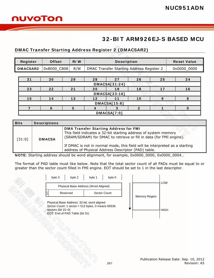
NUC951ADN
32-BIT ARM926EJ-S BASED MCU
Publication Release Date: Sep. 10, 2012 Revision: A5
267
DMAC Transfer Starting Address Register 2 (DMACSAR2)
Register Offset R/W Description Reset Value
DMACSAR2 0xB000_C808 R/W DMAC Transfer Starting Address Register 2 0x0000_0000
31 30 29 28 27 26 25 24 DMACSA[31:24]
23 22 21 20 19 18 17 16 DMACSA[23:16]
15 14 13 12 11 10 9 8 DMACSA[15:8]
7 6 5 4 3 2 1 0 DMACSA[7:0]
Bits Descriptions
[31:0] DMACSA
DMA Transfer Starting Address for FMI This field indicates a 32-bit starting address of system memory (SRAM/SDRAM) for DMAC to retrieve or fill in data (for FMI engine). If DMAC is not in normal mode, this field will be interpreted as a starting address of Physical Address Descriptor (PAD) table.
NOTE: Starting address should be word alignment, for example, 0x0000_0000, 0x0000_0004… The format of PAD table must like below. Note that the total sector count of all PADs must be equal to or greater than the sector count filled in FMI engine. EOT should be set to 1 in the last descriptor.
Memory Region
LOW
HIGH
Physical Base Address: 32-bit, word alignedSector Count: 1 sector = 512 bytes, 0 means 65536sectors (bit 15~0)EOT: End of PAD Table (bit 31)
byte 0byte 1byte 2byte 3
Physical Base Address (Word Aligned)
Sector CountReservedEO
T
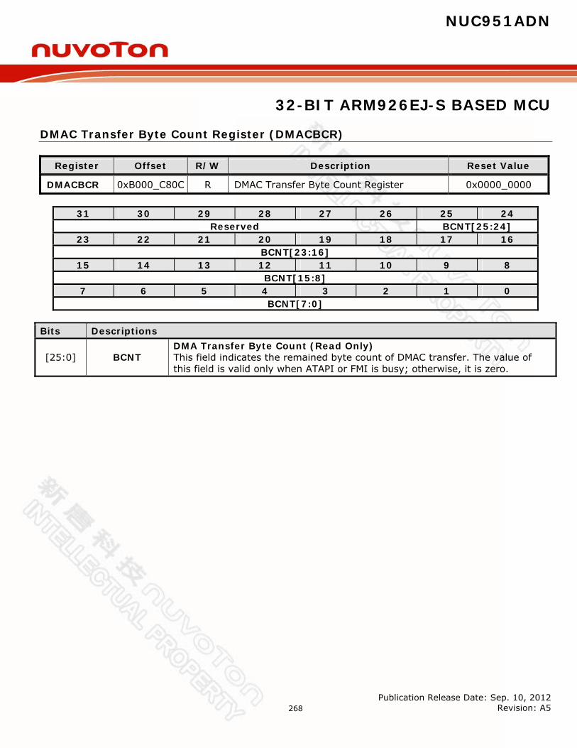
NUC951ADN
32-BIT ARM926EJ-S BASED MCU
Publication Release Date: Sep. 10, 2012 Revision: A5
268
DMAC Transfer Byte Count Register (DMACBCR)
Register Offset R/W Description Reset Value
DMACBCR 0xB000_C80C R DMAC Transfer Byte Count Register 0x0000_0000
31 30 29 28 27 26 25 24 Reserved BCNT[25:24]
23 22 21 20 19 18 17 16 BCNT[23:16]
15 14 13 12 11 10 9 8 BCNT[15:8]
7 6 5 4 3 2 1 0 BCNT[7:0]
Bits Descriptions
[25:0] BCNT DMA Transfer Byte Count (Read Only) This field indicates the remained byte count of DMAC transfer. The value of this field is valid only when ATAPI or FMI is busy; otherwise, it is zero.
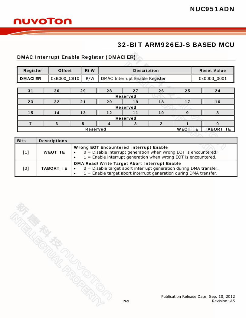
NUC951ADN
32-BIT ARM926EJ-S BASED MCU
Publication Release Date: Sep. 10, 2012 Revision: A5
269
DMAC Interrupt Enable Register (DMACIER)
Register Offset R/W Description Reset Value
DMACIER 0xB000_C810 R/W DMAC Interrupt Enable Register 0x0000_0001
31 30 29 28 27 26 25 24 Reserved
23 22 21 20 19 18 17 16 Reserved
15 14 13 12 11 10 9 8 Reserved
7 6 5 4 3 2 1 0 Reserved WEOT_IE TABORT_IE
Bits Descriptions
[1] WEOT_IE Wrong EOT Encountered Interrupt Enable 0 = Disable interrupt generation when wrong EOT is encountered. 1 = Enable interrupt generation when wrong EOT is encountered.
[0] TABORT_IE DMA Read/Write Target Abort Interrupt Enable 0 = Disable target abort interrupt generation during DMA transfer. 1 = Enable target abort interrupt generation during DMA transfer.

NUC951ADN
32-BIT ARM926EJ-S BASED MCU
Publication Release Date: Sep. 10, 2012 Revision: A5
270
DMAC Interrupt Status Register (DMACISR)
Register Offset R/W Description Reset Value
DMACISR 0xB000_C814 R/W DMAC Interrupt Status Register 0x0000_0000
31 30 29 28 27 26 25 24 Reserved
23 22 21 20 19 18 17 16 Reserved
15 14 13 12 11 10 9 8 Reserved
7 6 5 4 3 2 1 0 Reserved WEOT_IF TABORT_IF
Bits Descriptions
[1] WEOT_IF
Wrong EOT Encountered Interrupt Flag When DMA Scatter-Getter function is enabled, and EOT of the descriptor is encountered before DMA transfer finished (that means the total sector count of all PAD is less than the sector count of ATAPI or FMI), this bit will be set. 0 = No EOT encountered before DMA transfer finished. 1 = EOT encountered before DMA transfer finished. NOTE: This bit is read only, but can be cleared by writing ‘1’ to it.
[0] TABORT_IF
DMA Read/Write Target Abort Interrupt Flag 0 = No bus ERROR response received. 1 = Bus ERROR response received. NOTE: This bit is read only, but can be cleared by writing ‘1’ to it.
NOTE: When DMAC’s bus master received ERROR response, it means that target abort is happened. DMAC will stop transfer and respond this event to software, ATAPI and FMI; then go to IDLE state. When target abort occurred or WEOT_IF is set, suggest software reset DMAC and IP, and then transfer those data again.

NUC951ADN
32-BIT ARM926EJ-S BASED MCU
Publication Release Date: Sep. 10, 2012 Revision: A5
271
7.10 Flash Memory Interface Controller (FMI) The Flash Memory Interface (FMI) supports Secure Digital (SD, SDIO & MMC), Memory Stick (Memory stick PRO) and NAND-type flash. FMI is cooperated with DMAC to provide a fast data transfer between system memory and cards. There is one single 2048-byte buffer embedded in DMAC for temporary data storage. Due to DMAC only has single channel, that means only one interface can be active at the same time. Feature: Interface with DMAC for register read/write and data transfer 4 interfaces are provided: Secure Digital(2.0)/MMC(4.2), Memory Stick/Memory Stick PRO and
NAND-type flash Using single 2048-byte shared buffer for data exchange between system memory and cards
7.10.1 FMI Controller Registers Map R: read only, W: write only, R/W: both read and write Register Address R/W Description Reset Value
FMI Global Registers (FMI_BA = 0xB000_D000)
FMICSR 0xB000_D000 R/W Global Control and Status Register 0x0000_0000
FMIIER 0xB000_D004 R/W Global Interrupt Control Register 0x0000_0001
FMIISR 0xB000_D008 R/W Global Interrupt Status Register 0x0000_0000
Secure Digital Registers
SDCSR 0xB000_D020 R/W SD Control and Status Register 0x0101_0000
SDARG 0xB000_D024 R/W SD Command Argument Register 0x0000_0000
SDIER 0xB000_D028 R/W SD Interrupt Control Register 0x0000_0000
SDISR 0xB000_D02C R/W SD Interrupt Status Register 0x000X_008C
SDRSP0 0xB000_D030 R SD Receiving Response Token Register 0 0x0000_0000
SDRSP1 0xB000_D034 R SD Receiving Response Token Register 1 0x0000_0000
SDBLEN 0xB000_D038 R/W SD Block Length Register 0x0000_01FF
Memory Stick Registers
MSCSR 0xB000_D060 R/W Memory Stick Control and Status Register 0x0000_0008
MSIER 0xB000_D064 R/W Memory Stick Interrupt Control Register 0x0000_0000
MSISR 0xB000_D068 R/W Memory Stick Interrupt Status Register 0x0000_0000
MSBUF1 0xB000_D06C R/W Memory Stick Register Buffer 1 0x0000_0000
MSBUF2 0xB000_D070 R/W Memory Stick Register Buffer 2 0x0000_0000
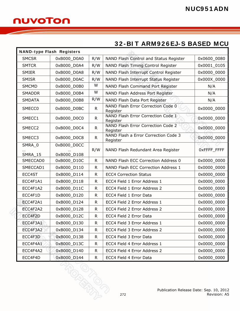
NUC951ADN
32-BIT ARM926EJ-S BASED MCU
Publication Release Date: Sep. 10, 2012 Revision: A5
272
NAND-type Flash Registers
SMCSR 0xB000_D0A0 R/W NAND Flash Control and Status Register 0x0600_0080
SMTCR 0xB000_D0A4 R/W NAND Flash Timing Control Register 0x0001_0105
SMIER 0xB000_D0A8 R/W NAND Flash Interrupt Control Register 0x0000_0000
SMISR 0xB000_D0AC R/W NAND Flash Interrupt Status Register 0x000X_0000
SMCMD 0xB000_D0B0 W NAND Flash Command Port Register N/A
SMADDR 0xB000_D0B4 W NAND Flash Address Port Register N/A
SMDATA 0xB000_D0B8 R/W NAND Flash Data Port Register N/A
SMECC0 0xB000_D0BC R NAND Flash Error Correction Code 0 Register 0x0000_0000
SMECC1 0xB000_D0C0 R NAND Flash Error Correction Code 1 Register 0x0000_0000
SMECC2 0xB000_D0C4 R NAND Flash Error Correction Code 2 Register 0x0000_0000
SMECC3 0xB000_D0C8 R NAND Flash a Error Correction Code 3 Register 0x0000_0000
SMRA_0 … SMRA_15
0xB000_D0CC …
0xB000_D108 R/W NAND Flash Redundant Area Register 0xFFFF_FFFF
SMECCAD0 0xB000_D10C R NAND Flash ECC Correction Address 0 0x0000_0000
SMECCAD1 0xB000_D110 R NAND Flash ECC Correction Address 1 0x0000_0000
ECC4ST 0xB000_D114 R ECC4 Correction Status 0x0000_0000
ECC4F1A1 0xB000_D118 R ECC4 Field 1 Error Address 1 0x0000_0000
ECC4F1A2 0xB000_D11C R ECC4 Field 1 Error Address 2 0x0000_0000
ECC4F1D 0xB000_D120 R ECC4 Field 1 Error Data 0x0000_0000
ECC4F2A1 0xB000_D124 R ECC4 Field 2 Error Address 1 0x0000_0000
ECC4F2A2 0xB000_D128 R ECC4 Field 2 Error Address 2 0x0000_0000
ECC4F2D 0xB000_D12C R ECC4 Field 2 Error Data 0x0000_0000
ECC4F3A1 0xB000_D130 R ECC4 Field 3 Error Address 1 0x0000_0000
ECC4F3A2 0xB000_D134 R ECC4 Field 3 Error Address 2 0x0000_0000
ECC4F3D 0xB000_D138 R ECC4 Field 3 Error Data 0x0000_0000
ECC4F4A1 0xB000_D13C R ECC4 Field 4 Error Address 1 0x0000_0000
ECC4F4A2 0xB000_D140 R ECC4 Field 4 Error Address 2 0x0000_0000
ECC4F4D 0xB000_D144 R ECC4 Field 4 Error Data 0x0000_0000

NUC951ADN
32-BIT ARM926EJ-S BASED MCU
Publication Release Date: Sep. 10, 2012 Revision: A5
273
7.10.2 Register Details
Global Control and Status Register (FMICSR)
Register Address R/W Description Reset Value
FMICSR 0xB000_D000 R/W Global Control and Status Register 0x0000_0000
31 30 29 28 27 26 25 24 Reserved
23 22 21 20 19 18 17 16 Reserved
15 14 13 12 11 10 9 8 Reserved
7 6 5 4 3 2 1 0 Reserved SM_EN MS_EN SD_EN SW_RST
Bits Descriptions
[3] SM_EN NAND-type Flash Functionality Enable 0 = Disable SM functionality of FMI. 1 = Enable SM functionality of FMI.
[2] MS_EN Memory Stick Functionality Enable 0 = Disable MS functionality of FMI. 1 = Enable MS functionality of FMI.
[1] SD_EN Secure Digital Functionality Enable 0 = Disable SD functionality of FMI. 1 = Enable SD functionality of FMI.
[0] SW_RST
Software Engine Reset 0 = Writing 0 to this bit has no effect. 1 = Writing 1 to this bit will reset all FMI engines. The contents of control register will not be cleared. This bit will auto clear after few clock cycles.
NOTE: Software can enable only one engine at one time, or FMI will work abnormal.
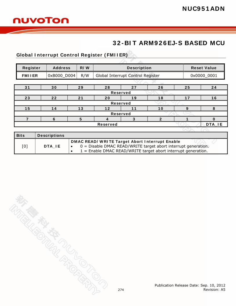
NUC951ADN
32-BIT ARM926EJ-S BASED MCU
Publication Release Date: Sep. 10, 2012 Revision: A5
274
Global Interrupt Control Register (FMIIER)
Register Address R/W Description Reset Value
FMIIER 0xB000_D004 R/W Global Interrupt Control Register 0x0000_0001
31 30 29 28 27 26 25 24 Reserved
23 22 21 20 19 18 17 16 Reserved
15 14 13 12 11 10 9 8 Reserved
7 6 5 4 3 2 1 0 Reserved DTA_IE
Bits Descriptions
[0] DTA_IE DMAC READ/WRITE Target Abort Interrupt Enable 0 = Disable DMAC READ/WRITE target abort interrupt generation. 1 = Enable DMAC READ/WRITE target abort interrupt generation.

NUC951ADN
32-BIT ARM926EJ-S BASED MCU
Publication Release Date: Sep. 10, 2012 Revision: A5
275
Global Interrupt Status Register (FMIISR)
Register Address R/W Description Reset Value
FMIISR 0xB000_D008 R/W Global Interrupt Status Register 0x0000_0000
31 30 29 28 27 26 25 24 Reserved
23 22 21 20 19 18 17 16 Reserved
15 14 13 12 11 10 9 8 Reserved
7 6 5 4 3 2 1 0 Reserved DTA_IF
Bits Descriptions
[0] DTA_IF
DMAC READ/WRITE Target Abort Interrupt Flag (Read Only) This bit indicates DMAC received an ERROR response from internal AHB bus during DMA read/write operation. When Target Abort is occurred, please reset all engine. 0 = No bus ERROR response received. 1 = Bus ERROR response received. NOTE: This bit is read only, but can be cleared by writing ‘1’ to it.
NOTE: No matter interrupt enable is turn on or not, the interrupt flag will be set when target condition is occurred.
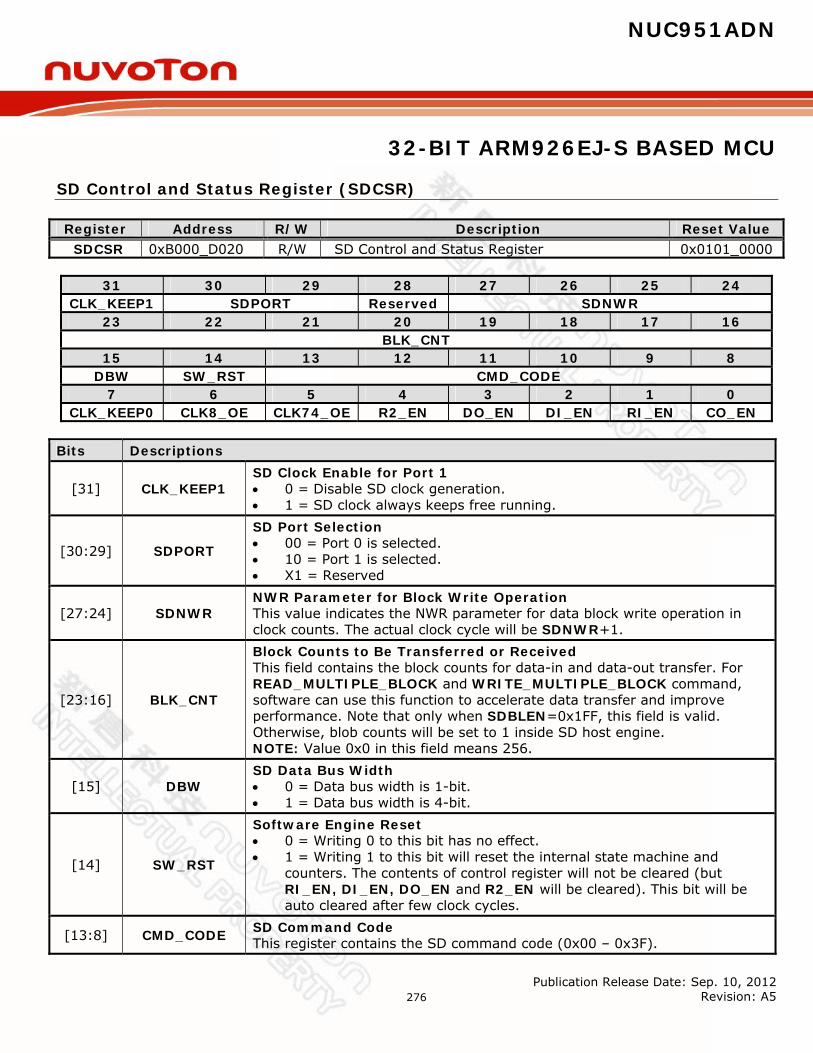
NUC951ADN
32-BIT ARM926EJ-S BASED MCU
Publication Release Date: Sep. 10, 2012 Revision: A5
276
SD Control and Status Register (SDCSR)
Register Address R/W Description Reset Value SDCSR 0xB000_D020 R/W SD Control and Status Register 0x0101_0000
31 30 29 28 27 26 25 24
CLK_KEEP1 SDPORT Reserved SDNWR 23 22 21 20 19 18 17 16
BLK_CNT 15 14 13 12 11 10 9 8
DBW SW_RST CMD_CODE 7 6 5 4 3 2 1 0
CLK_KEEP0 CLK8_OE CLK74_OE R2_EN DO_EN DI_EN RI_EN CO_EN Bits Descriptions
[31] CLK_KEEP1 SD Clock Enable for Port 1 0 = Disable SD clock generation. 1 = SD clock always keeps free running.
[30:29] SDPORT
SD Port Selection 00 = Port 0 is selected. 10 = Port 1 is selected. X1 = Reserved
[27:24] SDNWR NWR Parameter for Block Write Operation This value indicates the NWR parameter for data block write operation in clock counts. The actual clock cycle will be SDNWR+1.
[23:16] BLK_CNT
Block Counts to Be Transferred or Received This field contains the block counts for data-in and data-out transfer. For READ_MULTIPLE_BLOCK and WRITE_MULTIPLE_BLOCK command, software can use this function to accelerate data transfer and improve performance. Note that only when SDBLEN=0x1FF, this field is valid. Otherwise, blob counts will be set to 1 inside SD host engine. NOTE: Value 0x0 in this field means 256.
[15] DBW SD Data Bus Width 0 = Data bus width is 1-bit. 1 = Data bus width is 4-bit.
[14] SW_RST
Software Engine Reset 0 = Writing 0 to this bit has no effect. 1 = Writing 1 to this bit will reset the internal state machine and
counters. The contents of control register will not be cleared (but RI_EN, DI_EN, DO_EN and R2_EN will be cleared). This bit will be auto cleared after few clock cycles.
[13:8] CMD_CODE SD Command Code This register contains the SD command code (0x00 – 0x3F).
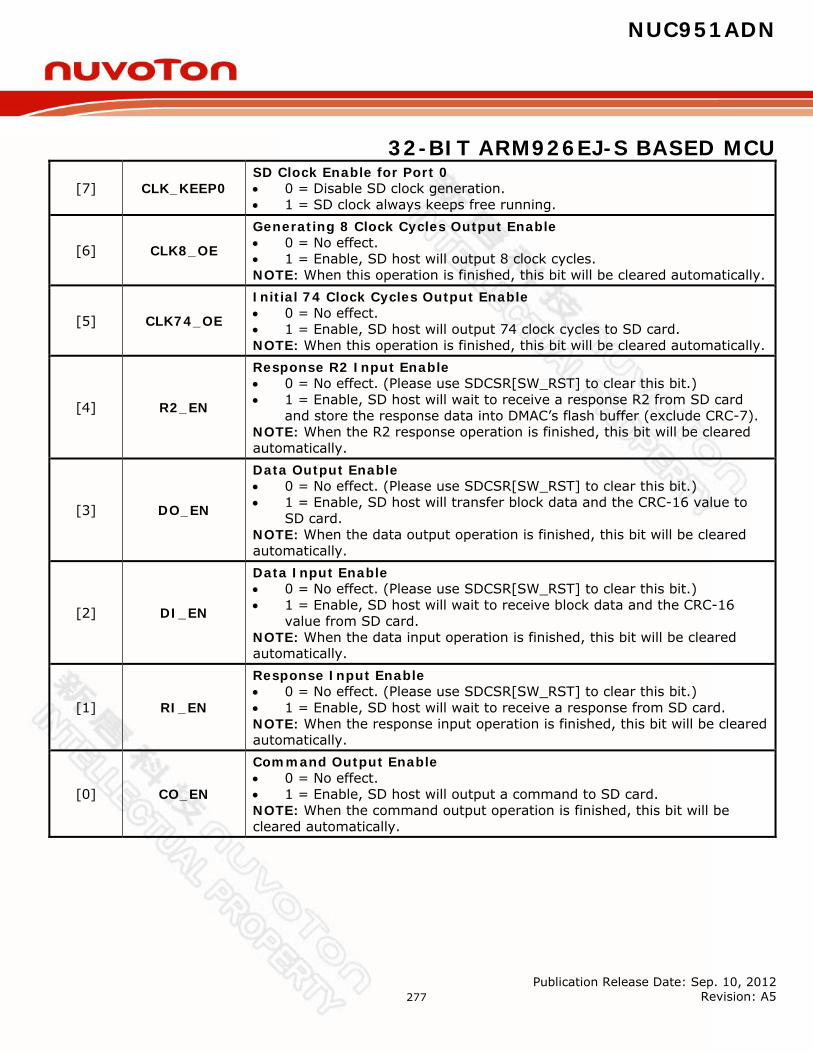
NUC951ADN
32-BIT ARM926EJ-S BASED MCU
Publication Release Date: Sep. 10, 2012 Revision: A5
277
[7] CLK_KEEP0 SD Clock Enable for Port 0 0 = Disable SD clock generation. 1 = SD clock always keeps free running.
[6] CLK8_OE
Generating 8 Clock Cycles Output Enable 0 = No effect. 1 = Enable, SD host will output 8 clock cycles. NOTE: When this operation is finished, this bit will be cleared automatically.
[5] CLK74_OE
Initial 74 Clock Cycles Output Enable 0 = No effect. 1 = Enable, SD host will output 74 clock cycles to SD card. NOTE: When this operation is finished, this bit will be cleared automatically.
[4] R2_EN
Response R2 Input Enable 0 = No effect. (Please use SDCSR[SW_RST] to clear this bit.) 1 = Enable, SD host will wait to receive a response R2 from SD card
and store the response data into DMAC’s flash buffer (exclude CRC-7). NOTE: When the R2 response operation is finished, this bit will be cleared automatically.
[3] DO_EN
Data Output Enable 0 = No effect. (Please use SDCSR[SW_RST] to clear this bit.) 1 = Enable, SD host will transfer block data and the CRC-16 value to
SD card. NOTE: When the data output operation is finished, this bit will be cleared automatically.
[2] DI_EN
Data Input Enable 0 = No effect. (Please use SDCSR[SW_RST] to clear this bit.) 1 = Enable, SD host will wait to receive block data and the CRC-16
value from SD card. NOTE: When the data input operation is finished, this bit will be cleared automatically.
[1] RI_EN
Response Input Enable 0 = No effect. (Please use SDCSR[SW_RST] to clear this bit.) 1 = Enable, SD host will wait to receive a response from SD card. NOTE: When the response input operation is finished, this bit will be cleared automatically.
[0] CO_EN
Command Output Enable 0 = No effect. 1 = Enable, SD host will output a command to SD card. NOTE: When the command output operation is finished, this bit will be cleared automatically.
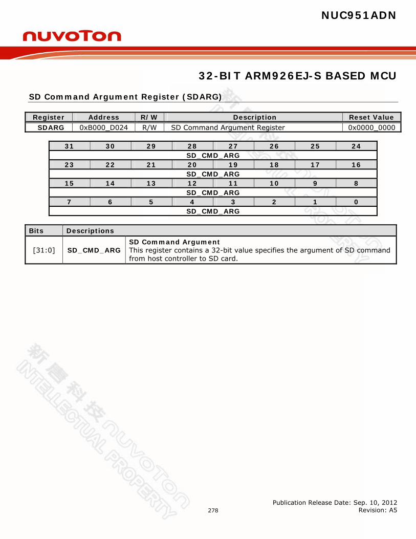
NUC951ADN
32-BIT ARM926EJ-S BASED MCU
Publication Release Date: Sep. 10, 2012 Revision: A5
278
SD Command Argument Register (SDARG)
Register Address R/W Description Reset Value SDARG 0xB000_D024 R/W SD Command Argument Register 0x0000_0000
31 30 29 28 27 26 25 24
SD_CMD_ARG 23 22 21 20 19 18 17 16
SD_CMD_ARG 15 14 13 12 11 10 9 8
SD_CMD_ARG 7 6 5 4 3 2 1 0
SD_CMD_ARG Bits Descriptions
[31:0] SD_CMD_ARG SD Command Argument This register contains a 32-bit value specifies the argument of SD command from host controller to SD card.
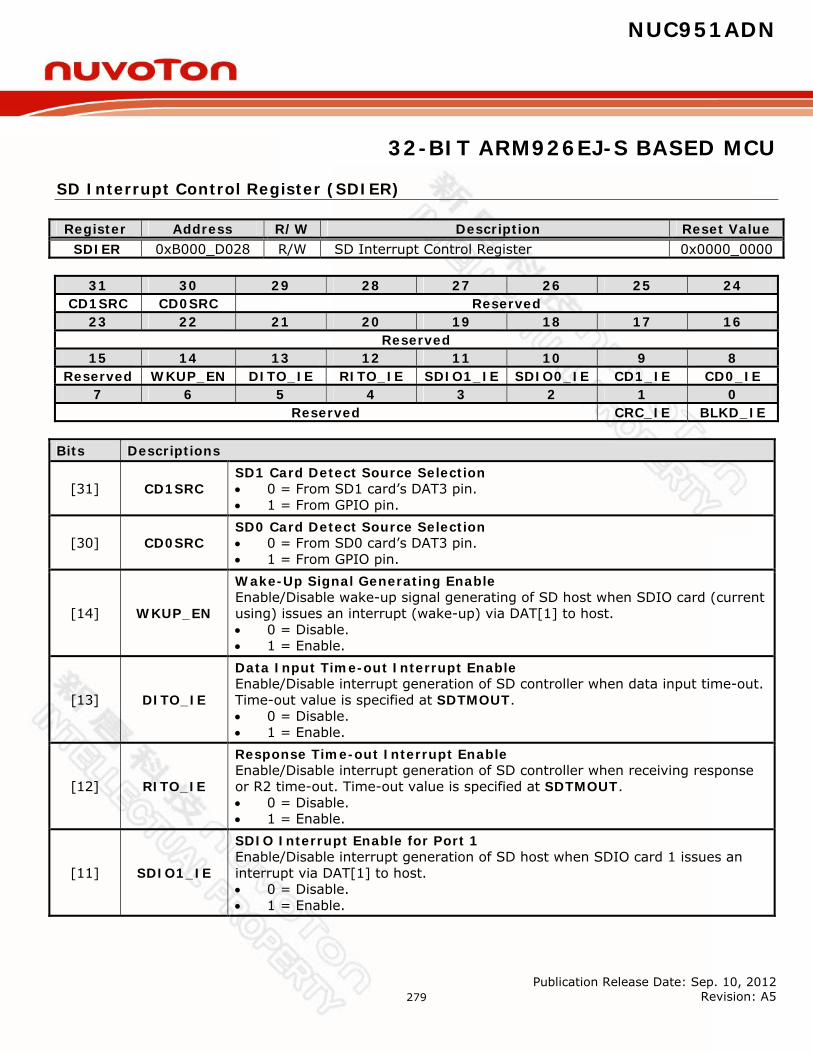
NUC951ADN
32-BIT ARM926EJ-S BASED MCU
Publication Release Date: Sep. 10, 2012 Revision: A5
279
SD Interrupt Control Register (SDIER)
Register Address R/W Description Reset Value SDIER 0xB000_D028 R/W SD Interrupt Control Register 0x0000_0000
31 30 29 28 27 26 25 24
CD1SRC CD0SRC Reserved 23 22 21 20 19 18 17 16
Reserved 15 14 13 12 11 10 9 8
Reserved WKUP_EN DITO_IE RITO_IE SDIO1_IE SDIO0_IE CD1_IE CD0_IE 7 6 5 4 3 2 1 0
Reserved CRC_IE BLKD_IE Bits Descriptions
[31] CD1SRC SD1 Card Detect Source Selection 0 = From SD1 card’s DAT3 pin. 1 = From GPIO pin.
[30] CD0SRC SD0 Card Detect Source Selection 0 = From SD0 card’s DAT3 pin. 1 = From GPIO pin.
[14] WKUP_EN
Wake-Up Signal Generating Enable Enable/Disable wake-up signal generating of SD host when SDIO card (current using) issues an interrupt (wake-up) via DAT[1] to host. 0 = Disable. 1 = Enable.
[13] DITO_IE
Data Input Time-out Interrupt Enable Enable/Disable interrupt generation of SD controller when data input time-out. Time-out value is specified at SDTMOUT. 0 = Disable. 1 = Enable.
[12] RITO_IE
Response Time-out Interrupt Enable Enable/Disable interrupt generation of SD controller when receiving response or R2 time-out. Time-out value is specified at SDTMOUT. 0 = Disable. 1 = Enable.
[11] SDIO1_IE
SDIO Interrupt Enable for Port 1 Enable/Disable interrupt generation of SD host when SDIO card 1 issues an interrupt via DAT[1] to host. 0 = Disable. 1 = Enable.
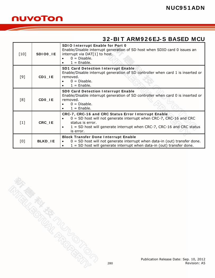
NUC951ADN
32-BIT ARM926EJ-S BASED MCU
Publication Release Date: Sep. 10, 2012 Revision: A5
280
[10] SDIO0_IE
SDIO Interrupt Enable for Port 0 Enable/Disable interrupt generation of SD host when SDIO card 0 issues an interrupt via DAT[1] to host. 0 = Disable. 1 = Enable.
[9] CD1_IE
SD1 Card Detection Interrupt Enable Enable/Disable interrupt generation of SD controller when card 1 is inserted or removed. 0 = Disable. 1 = Enable.
[8] CD0_IE
SD0 Card Detection Interrupt Enable Enable/Disable interrupt generation of SD controller when card 0 is inserted or removed. 0 = Disable. 1 = Enable.
[1] CRC_IE
CRC-7, CRC-16 and CRC Status Error Interrupt Enable 0 = SD host will not generate interrupt when CRC-7, CRC-16 and CRC
status is error. 1 = SD host will generate interrupt when CRC-7, CRC-16 and CRC status
is error.
[0] BLKD_IE Block Transfer Done Interrupt Enable 0 = SD host will not generate interrupt when data-in (out) transfer done. 1 = SD host will generate interrupt when data-in (out) transfer done.
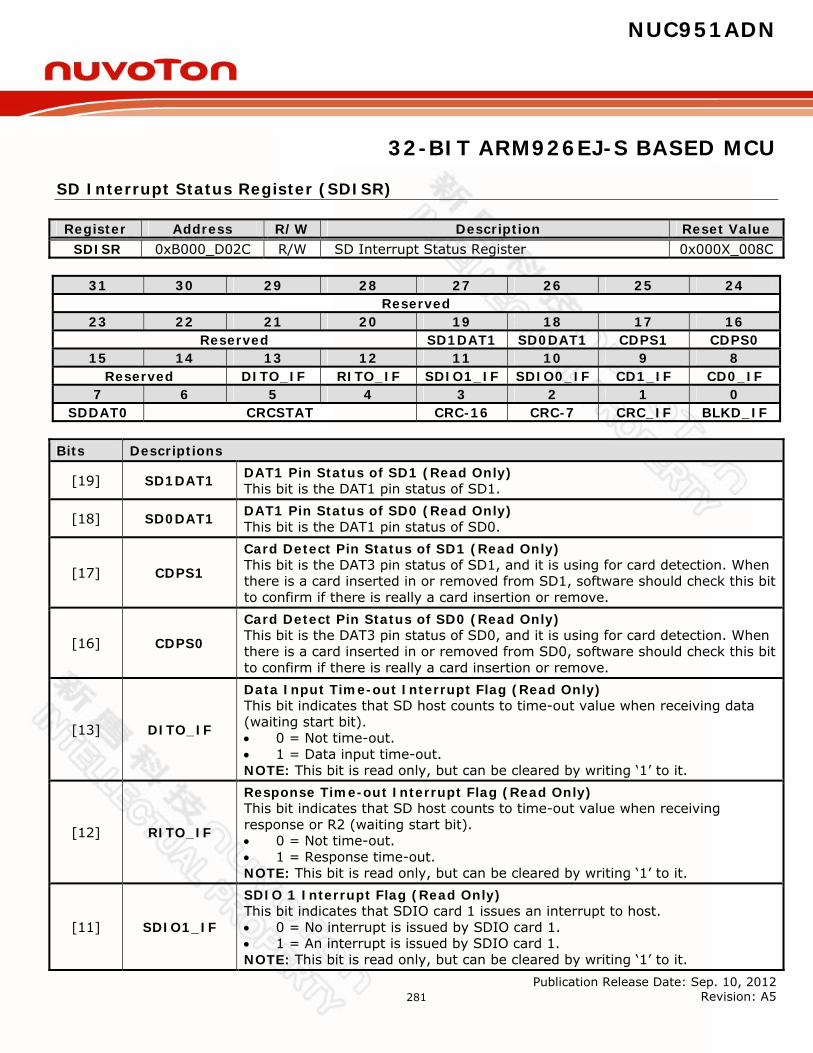
NUC951ADN
32-BIT ARM926EJ-S BASED MCU
Publication Release Date: Sep. 10, 2012 Revision: A5
281
SD Interrupt Status Register (SDISR)
Register Address R/W Description Reset Value SDISR 0xB000_D02C R/W SD Interrupt Status Register 0x000X_008C
31 30 29 28 27 26 25 24
Reserved 23 22 21 20 19 18 17 16
Reserved SD1DAT1 SD0DAT1 CDPS1 CDPS0 15 14 13 12 11 10 9 8
Reserved DITO_IF RITO_IF SDIO1_IF SDIO0_IF CD1_IF CD0_IF 7 6 5 4 3 2 1 0
SDDAT0 CRCSTAT CRC-16 CRC-7 CRC_IF BLKD_IF Bits Descriptions
[19] SD1DAT1 DAT1 Pin Status of SD1 (Read Only) This bit is the DAT1 pin status of SD1.
[18] SD0DAT1 DAT1 Pin Status of SD0 (Read Only) This bit is the DAT1 pin status of SD0.
[17] CDPS1
Card Detect Pin Status of SD1 (Read Only) This bit is the DAT3 pin status of SD1, and it is using for card detection. When there is a card inserted in or removed from SD1, software should check this bit to confirm if there is really a card insertion or remove.
[16] CDPS0
Card Detect Pin Status of SD0 (Read Only) This bit is the DAT3 pin status of SD0, and it is using for card detection. When there is a card inserted in or removed from SD0, software should check this bit to confirm if there is really a card insertion or remove.
[13] DITO_IF
Data Input Time-out Interrupt Flag (Read Only) This bit indicates that SD host counts to time-out value when receiving data (waiting start bit). 0 = Not time-out. 1 = Data input time-out. NOTE: This bit is read only, but can be cleared by writing ‘1’ to it.
[12] RITO_IF
Response Time-out Interrupt Flag (Read Only) This bit indicates that SD host counts to time-out value when receiving response or R2 (waiting start bit). 0 = Not time-out. 1 = Response time-out. NOTE: This bit is read only, but can be cleared by writing ‘1’ to it.
[11] SDIO1_IF
SDIO 1 Interrupt Flag (Read Only) This bit indicates that SDIO card 1 issues an interrupt to host. 0 = No interrupt is issued by SDIO card 1. 1 = An interrupt is issued by SDIO card 1. NOTE: This bit is read only, but can be cleared by writing ‘1’ to it.
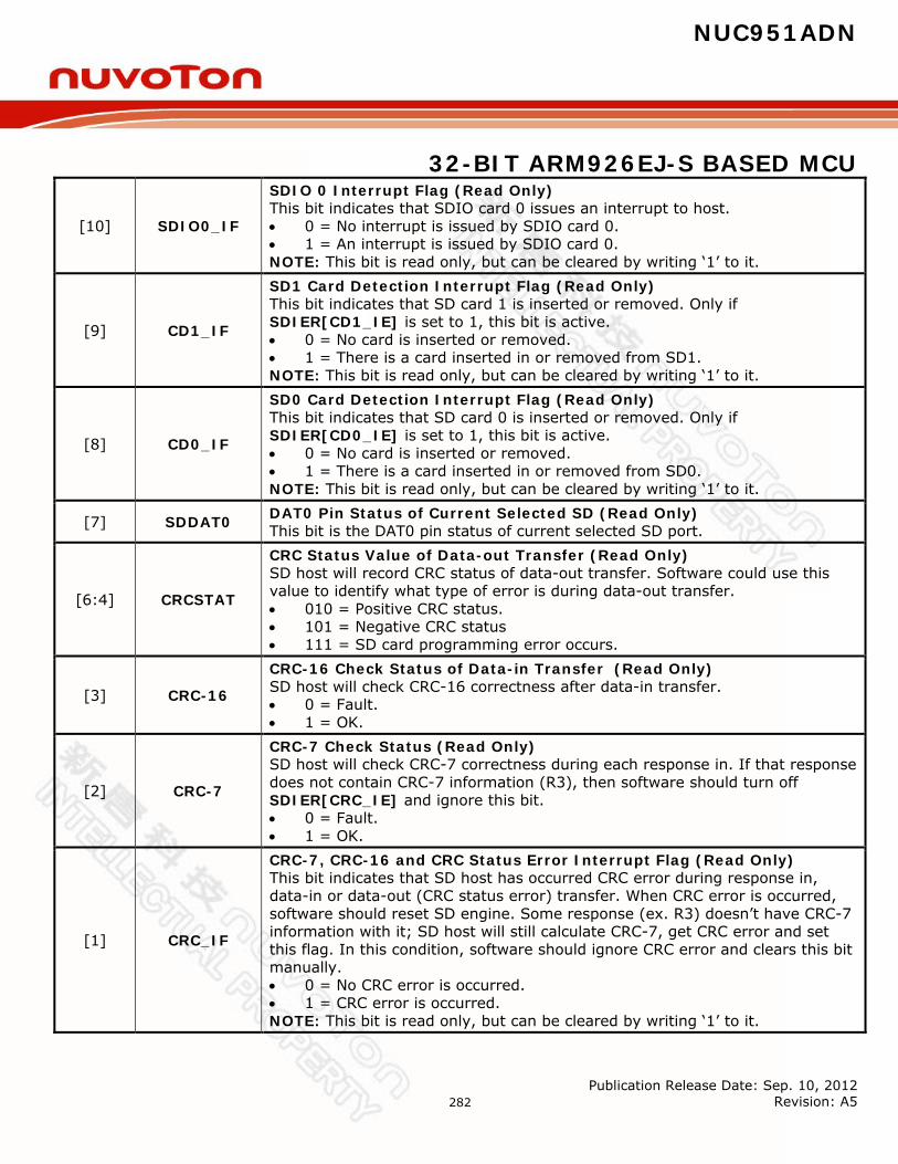
NUC951ADN
32-BIT ARM926EJ-S BASED MCU
Publication Release Date: Sep. 10, 2012 Revision: A5
282
[10] SDIO0_IF
SDIO 0 Interrupt Flag (Read Only) This bit indicates that SDIO card 0 issues an interrupt to host. 0 = No interrupt is issued by SDIO card 0. 1 = An interrupt is issued by SDIO card 0. NOTE: This bit is read only, but can be cleared by writing ‘1’ to it.
[9] CD1_IF
SD1 Card Detection Interrupt Flag (Read Only) This bit indicates that SD card 1 is inserted or removed. Only if SDIER[CD1_IE] is set to 1, this bit is active. 0 = No card is inserted or removed. 1 = There is a card inserted in or removed from SD1. NOTE: This bit is read only, but can be cleared by writing ‘1’ to it.
[8] CD0_IF
SD0 Card Detection Interrupt Flag (Read Only) This bit indicates that SD card 0 is inserted or removed. Only if SDIER[CD0_IE] is set to 1, this bit is active. 0 = No card is inserted or removed. 1 = There is a card inserted in or removed from SD0. NOTE: This bit is read only, but can be cleared by writing ‘1’ to it.
[7] SDDAT0 DAT0 Pin Status of Current Selected SD (Read Only) This bit is the DAT0 pin status of current selected SD port.
[6:4] CRCSTAT
CRC Status Value of Data-out Transfer (Read Only) SD host will record CRC status of data-out transfer. Software could use this value to identify what type of error is during data-out transfer. 010 = Positive CRC status. 101 = Negative CRC status 111 = SD card programming error occurs.
[3] CRC-16
CRC-16 Check Status of Data-in Transfer (Read Only) SD host will check CRC-16 correctness after data-in transfer. 0 = Fault. 1 = OK.
[2] CRC-7
CRC-7 Check Status (Read Only) SD host will check CRC-7 correctness during each response in. If that response does not contain CRC-7 information (R3), then software should turn off SDIER[CRC_IE] and ignore this bit. 0 = Fault. 1 = OK.
[1] CRC_IF
CRC-7, CRC-16 and CRC Status Error Interrupt Flag (Read Only) This bit indicates that SD host has occurred CRC error during response in, data-in or data-out (CRC status error) transfer. When CRC error is occurred, software should reset SD engine. Some response (ex. R3) doesn’t have CRC-7 information with it; SD host will still calculate CRC-7, get CRC error and set this flag. In this condition, software should ignore CRC error and clears this bit manually. 0 = No CRC error is occurred. 1 = CRC error is occurred. NOTE: This bit is read only, but can be cleared by writing ‘1’ to it.
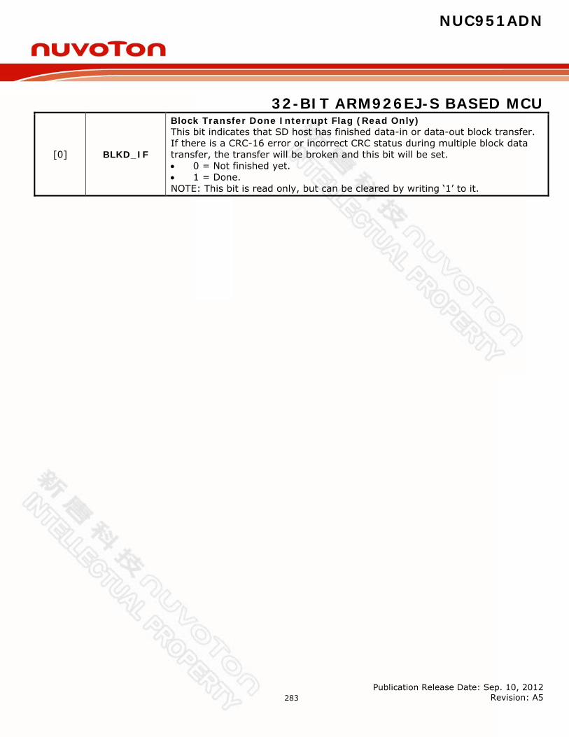
NUC951ADN
32-BIT ARM926EJ-S BASED MCU
Publication Release Date: Sep. 10, 2012 Revision: A5
283
[0] BLKD_IF
Block Transfer Done Interrupt Flag (Read Only) This bit indicates that SD host has finished data-in or data-out block transfer. If there is a CRC-16 error or incorrect CRC status during multiple block data transfer, the transfer will be broken and this bit will be set. 0 = Not finished yet. 1 = Done. NOTE: This bit is read only, but can be cleared by writing ‘1’ to it.
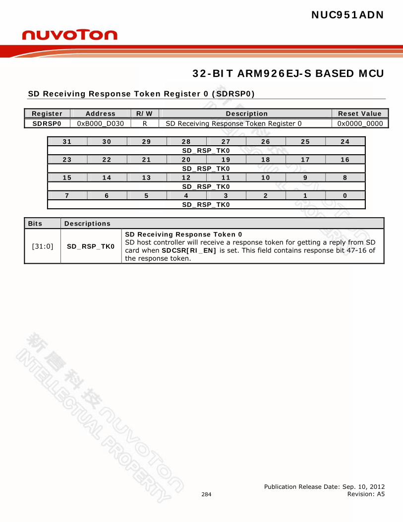
NUC951ADN
32-BIT ARM926EJ-S BASED MCU
Publication Release Date: Sep. 10, 2012 Revision: A5
284
SD Receiving Response Token Register 0 (SDRSP0)
Register Address R/W Description Reset Value SDRSP0 0xB000_D030 R SD Receiving Response Token Register 0 0x0000_0000
31 30 29 28 27 26 25 24
SD_RSP_TK0 23 22 21 20 19 18 17 16
SD_RSP_TK0 15 14 13 12 11 10 9 8
SD_RSP_TK0 7 6 5 4 3 2 1 0
SD_RSP_TK0 Bits Descriptions
[31:0] SD_RSP_TK0
SD Receiving Response Token 0 SD host controller will receive a response token for getting a reply from SD card when SDCSR[RI_EN] is set. This field contains response bit 47-16 of the response token.

NUC951ADN
32-BIT ARM926EJ-S BASED MCU
Publication Release Date: Sep. 10, 2012 Revision: A5
285
SD Receiving Response Token Register 1 (SDRSP1)
Register Address R/W Description Reset Value SDRSP1 0xB000_D034 R SD Receiving Response Token Register 1 0x0000_0000
31 30 29 28 27 26 25 24
Reserved 23 22 21 20 19 18 17 16
Reserved 15 14 13 12 11 10 9 8
Reserved 7 6 5 4 3 2 1 0
SD_RSP_TK1 Bits Descriptions
[7:0] SD_RSP_TK1
SD Receiving Response Token 1 SD host controller will receive a response token for getting a reply from SD card when SDCSR[RI_EN] is set. This register contains the bit 15-8 of the response token.
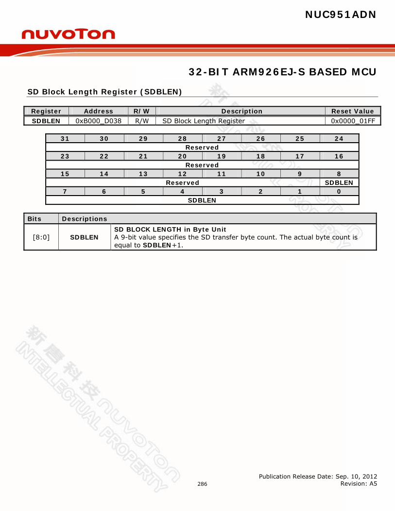
NUC951ADN
32-BIT ARM926EJ-S BASED MCU
Publication Release Date: Sep. 10, 2012 Revision: A5
286
SD Block Length Register (SDBLEN)
Register Address R/W Description Reset Value SDBLEN 0xB000_D038 R/W SD Block Length Register 0x0000_01FF
31 30 29 28 27 26 25 24
Reserved 23 22 21 20 19 18 17 16
Reserved 15 14 13 12 11 10 9 8
Reserved SDBLEN 7 6 5 4 3 2 1 0
SDBLEN Bits Descriptions
[8:0] SDBLEN SD BLOCK LENGTH in Byte Unit A 9-bit value specifies the SD transfer byte count. The actual byte count is equal to SDBLEN+1.
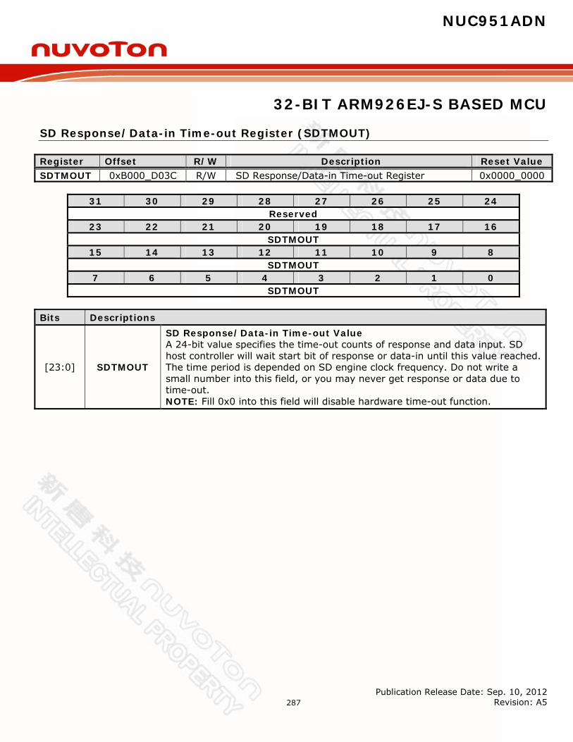
NUC951ADN
32-BIT ARM926EJ-S BASED MCU
Publication Release Date: Sep. 10, 2012 Revision: A5
287
SD Response/Data-in Time-out Register (SDTMOUT)
Register Offset R/W Description Reset Value SDTMOUT 0xB000_D03C R/W SD Response/Data-in Time-out Register 0x0000_0000
31 30 29 28 27 26 25 24 Reserved
23 22 21 20 19 18 17 16 SDTMOUT
15 14 13 12 11 10 9 8 SDTMOUT
7 6 5 4 3 2 1 0 SDTMOUT
Bits Descriptions
[23:0] SDTMOUT
SD Response/Data-in Time-out Value A 24-bit value specifies the time-out counts of response and data input. SD host controller will wait start bit of response or data-in until this value reached. The time period is depended on SD engine clock frequency. Do not write a small number into this field, or you may never get response or data due to time-out. NOTE: Fill 0x0 into this field will disable hardware time-out function.
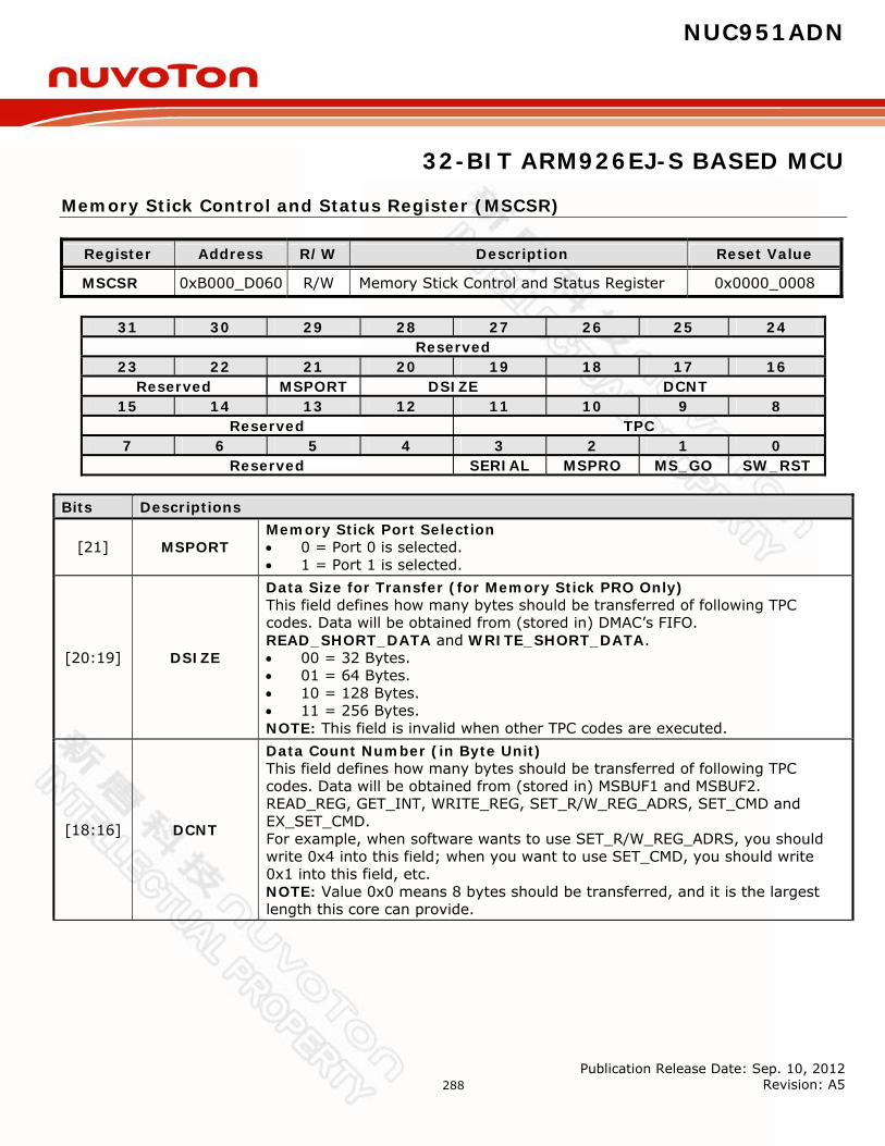
NUC951ADN
32-BIT ARM926EJ-S BASED MCU
Publication Release Date: Sep. 10, 2012 Revision: A5
288
Memory Stick Control and Status Register (MSCSR)
Register Address R/W Description Reset Value
MSCSR 0xB000_D060 R/W Memory Stick Control and Status Register 0x0000_0008
31 30 29 28 27 26 25 24 Reserved
23 22 21 20 19 18 17 16 Reserved MSPORT DSIZE DCNT
15 14 13 12 11 10 9 8 Reserved TPC
7 6 5 4 3 2 1 0 Reserved SERIAL MSPRO MS_GO SW_RST
Bits Descriptions
[21] MSPORT Memory Stick Port Selection 0 = Port 0 is selected. 1 = Port 1 is selected.
[20:19] DSIZE
Data Size for Transfer (for Memory Stick PRO Only) This field defines how many bytes should be transferred of following TPC codes. Data will be obtained from (stored in) DMAC’s FIFO. READ_SHORT_DATA and WRITE_SHORT_DATA. 00 = 32 Bytes. 01 = 64 Bytes. 10 = 128 Bytes. 11 = 256 Bytes. NOTE: This field is invalid when other TPC codes are executed.
[18:16] DCNT
Data Count Number (in Byte Unit) This field defines how many bytes should be transferred of following TPC codes. Data will be obtained from (stored in) MSBUF1 and MSBUF2. READ_REG, GET_INT, WRITE_REG, SET_R/W_REG_ADRS, SET_CMD and EX_SET_CMD. For example, when software wants to use SET_R/W_REG_ADRS, you should write 0x4 into this field; when you want to use SET_CMD, you should write 0x1 into this field, etc. NOTE: Value 0x0 means 8 bytes should be transferred, and it is the largest length this core can provide.
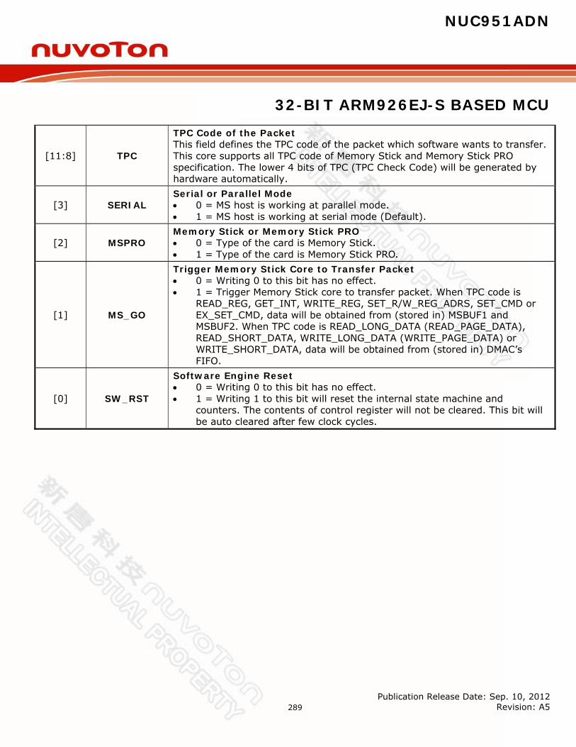
NUC951ADN
32-BIT ARM926EJ-S BASED MCU
Publication Release Date: Sep. 10, 2012 Revision: A5
289
[11:8] TPC
TPC Code of the Packet This field defines the TPC code of the packet which software wants to transfer. This core supports all TPC code of Memory Stick and Memory Stick PRO specification. The lower 4 bits of TPC (TPC Check Code) will be generated by hardware automatically.
[3] SERIAL Serial or Parallel Mode 0 = MS host is working at parallel mode. 1 = MS host is working at serial mode (Default).
[2] MSPRO Memory Stick or Memory Stick PRO 0 = Type of the card is Memory Stick. 1 = Type of the card is Memory Stick PRO.
[1] MS_GO
Trigger Memory Stick Core to Transfer Packet 0 = Writing 0 to this bit has no effect. 1 = Trigger Memory Stick core to transfer packet. When TPC code is
READ_REG, GET_INT, WRITE_REG, SET_R/W_REG_ADRS, SET_CMD or EX_SET_CMD, data will be obtained from (stored in) MSBUF1 and MSBUF2. When TPC code is READ_LONG_DATA (READ_PAGE_DATA), READ_SHORT_DATA, WRITE_LONG_DATA (WRITE_PAGE_DATA) or WRITE_SHORT_DATA, data will be obtained from (stored in) DMAC’s FIFO.
[0] SW_RST
Software Engine Reset 0 = Writing 0 to this bit has no effect. 1 = Writing 1 to this bit will reset the internal state machine and
counters. The contents of control register will not be cleared. This bit will be auto cleared after few clock cycles.

NUC951ADN
32-BIT ARM926EJ-S BASED MCU
Publication Release Date: Sep. 10, 2012 Revision: A5
290
Memory Stick Interrupt Control Register (MSIER)
Register Address R/W Description Reset Value
MSIER 0xB000_D064 R/W Memory Stick Interrupt Control Register 0x0000_0000
31 30 29 28 27 26 25 24 Reserved
23 22 21 20 19 18 17 16 Reserved CD1_IE CD0_IE
15 14 13 12 11 10 9 8 Reserved
7 6 5 4 3 2 1 0 Reserved CRC_IE BSYTO_IE INTTO_IE MSINT_IE PKT_IE
Bits Descriptions
[17] CD1_IE
MS Card Detection 1 Interrupt Enable Enable/Disable Interrupt generation of MS controller when card 1 is inserted or removed. 0 = Disable. 1 = Enable.
[16] CD0_IE
MS Card Detection 0 Interrupt Enable Enable/Disable Interrupt generation of MS controller when card 0 is inserted or removed. 0 = Disable. 1 = Enable.
[4] CRC_IE CRC-16 Error Interrupt Enable 0 = the core will not generate interrupt when CRC-16 is error. 1 = the core will generate interrupt when CRC-16 is error.
[3] BSYTO_IE Busy to Ready Check Timeout Interrupt Enable 0 = Disable Busy to Ready check timeout interrupt. 1 = Enable Busy to Ready check timeout interrupt.
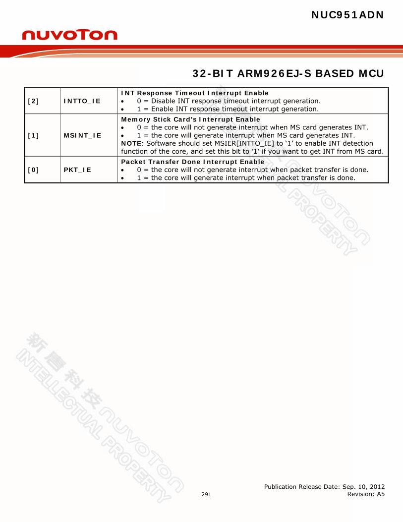
NUC951ADN
32-BIT ARM926EJ-S BASED MCU
Publication Release Date: Sep. 10, 2012 Revision: A5
291
[2] INTTO_IE INT Response Timeout Interrupt Enable 0 = Disable INT response timeout interrupt generation. 1 = Enable INT response timeout interrupt generation.
[1] MSINT_IE
Memory Stick Card’s Interrupt Enable 0 = the core will not generate interrupt when MS card generates INT. 1 = the core will generate interrupt when MS card generates INT. NOTE: Software should set MSIER[INTTO_IE] to ‘1’ to enable INT detection function of the core, and set this bit to ‘1’ if you want to get INT from MS card.
[0] PKT_IE Packet Transfer Done Interrupt Enable 0 = the core will not generate interrupt when packet transfer is done. 1 = the core will generate interrupt when packet transfer is done.
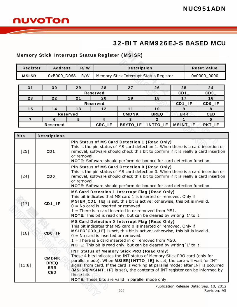
NUC951ADN
32-BIT ARM926EJ-S BASED MCU
Publication Release Date: Sep. 10, 2012 Revision: A5
292
Memory Stick Interrupt Status Register (MSISR)
Register Address R/W Description Reset Value
MSISR 0xB000_D068 R/W Memory Stick Interrupt Status Register 0x0000_0000
31 30 29 28 27 26 25 24 Reserved CD1_ CD0_
23 22 21 20 19 18 17 16 Reserved CD1_IF CD0_IF
15 14 13 12 11 10 9 8 Reserved CMDNK BREQ ERR CED
7 6 5 4 3 2 1 0 Reserved CRC_IF BSYTO_IF INTTO_IF MSINT_IF PKT_IF
Bits Descriptions
[25] CD1_
Pin Status of MS Card Detection 1 (Read Only) This is the pin status of MS card detection 1. When there is a card insertion or removal, software should check this bit to confirm if it is really a card insertion or removal. NOTE: Software should perform de-bounce for card detection function.
[24] CD0_
Pin Status of MS Card Detection 0 (Read Only) This is the pin status of MS card detection 0. When there is a card insertion or removal, software should check this bit to confirm if it is really a card insertion or removal. NOTE: Software should perform de-bounce for card detection function.
[17] CD1_IF
MS Card Detection 1 Interrupt Flag (Read Only) This bit indicates that MS card 1 is inserted or removed. Only if MSIER[CD1_IE] is set, this bit is active; otherwise, this bit is invalid. 0 = No card is inserted or removed. 1 = There is a card inserted in or removed from MS1. NOTE: This bit is read only, but can be cleared by writing ‘1’ to it.
[16] CD0_IF
MS Card Detection 0 Interrupt Flag (Read Only) This bit indicates that MS card 0 is inserted or removed. Only if MSIER[CD0_IE] is set, this bit is active; otherwise, this bit is invalid. 0 = No card is inserted or removed. 1 = There is a card inserted in or removed from MS0. NOTE: This bit is read only, but can be cleared by writing ‘1’ to it.
[11:8]
CMDNK BREQ ERR CED
INT Status of Memory Stick PRO (Read Only) These 4 bits indicates the INT status of Memory Stick PRO card (only for parallel mode). When MSIER[INTTO_IE] is set, the core will wait for INT signal from card. If the card is working at parallel mode; after INT is occurred (MSISR[MSINT_IF] is set), the contents of INT register can be informed by these bits. NOTE: These bits are valid in parallel mode only.
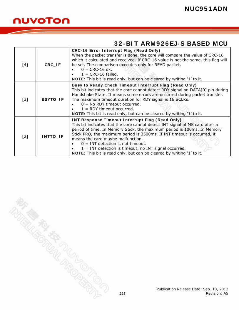
NUC951ADN
32-BIT ARM926EJ-S BASED MCU
Publication Release Date: Sep. 10, 2012 Revision: A5
293
[4] CRC_IF
CRC-16 Error Interrupt Flag (Read Only) When the packet transfer is done, the core will compare the value of CRC-16 which it calculated and received. If CRC-16 value is not the same, this flag will be set. The comparison executes only for READ packet. 0 = CRC-16 ok. 1 = CRC-16 failed. NOTE: This bit is read only, but can be cleared by writing ‘1’ to it.
[3] BSYTO_IF
Busy to Ready Check Timeout Interrupt Flag (Read Only) This bit indicates that the core cannot detect RDY signal on DATA[0] pin during Handshake State. It means some errors are occurred during packet transfer. The maximum timeout duration for RDY signal is 16 SCLKs. 0 = No RDY timeout occurred. 1 = RDY timeout occurred. NOTE: This bit is read only, but can be cleared by writing ‘1’ to it.
[2] INTTO_IF
INT Response Timeout Interrupt Flag (Read Only) This bit indicates that the core cannot detect INT signal of MS card after a period of time. In Memory Stick, the maximum period is 100ms. In Memory Stick PRO, the maximum period is 3500ms. If INT timeout is occurred, it means the card maybe malfunction. 0 = INT detection is not timeout. 1 = INT detection is timeout, no INT signal occurred. NOTE: This bit is read only, but can be cleared by writing ‘1’ to it.
NUC951ADN
32-BIT ARM926EJ-S BASED MCU
Publication Release Date: Sep. 10, 2012 Revision: A5
294
[1] MSINT_IF
Memory Stick Card’s Interrupt Flag (Read Only) Memory Stick will generate INT signal after some TPC codes are executed, ex. SET_CMD. This bit indicates that Memory Stick has generated INT signal after TPC code execution. This core will check INT for software only when MSIER[INTTO_IE] is set to ‘1’, or this bit is invalid. 0 = No INT signal is detected. 1 = INT signal is detected. NOTE: This bit is read only, but can be cleared by writing ‘1’ to it.
[0] PKT_IF
Packet Transfer Done Interrupt Flag (Read Only) This bit indicates that the whole packet transfer is done. The four states of Memory Stick are BS1, BS2, BS3 and BS0. 0 = Packet transfer is not done yet. 1 = Packet transfer is done. NOTE: This bit is read only, but can be cleared by writing ‘1’ to it.
NOTE: No matter interrupt enable is turn on or not, the interrupt flag will be set when target condition is occurred.
NUC951ADN
32-BIT ARM926EJ-S BASED MCU
Publication Release Date: Sep. 10, 2012 Revision: A5
295
Memory Stick Register Buffer 1 (MSBUF1)
Memory Stick Register Buffer 2 (MSBUF2)
Register Address R/W Description Reset Value
MSBUF1 MSBUF2
0xB000_D06C 0xB000_D070 R/W Memory Stick Register Buffer 1
Memory Stick Register Buffer 2 0x0000_0x0000
31 30 29 28 27 26 25 24
DATA[31:24] 23 22 21 20 19 18 17 16
DATA[23:16] 15 14 13 12 11 10 9 8
DATA[15:8] 7 6 5 4 3 2 1 0
DATA[7:0] Bits Descriptions
[31:0] DATA
Data Content of Packet Transfer This field contains the data of READ/WRITE TPC codes. When software uses following TPC codes, data will be obtained from (stored in) this field. READ_REG, GET_INT, WRITE_REG, SET_R/W_REG_ADRS, SET_CMD and EX_SET_CMD. This core will always send (store) data from MSB of MSBUF2. For example, if software wants to WRITE a packet with 1 byte data, you should put the data at MSBUF2[31:24] and write 0x1 into MSCSR[DCNT] then trigger the core. The order of transfer will be MSBUF2[31], MSBUF2[30] …, MSBUF2[24]. If you want to WRITE a packet with 6 bytes data, you should put the data at MSBUF2[31:0] and MSBUF1[31:16] and write 0x6 into MSCSR[DCNT] then trigger the core. The order of transfer will be MSBUF2[31:24], … MSBUF2[7:0], MSBUF1[31:24], MSBUF1[23:16]. The same order will be applied to READ packet.
BYTE 5
BYTE 6
BYTE 7
BYTE 8
MSBUF1
BYTE 1
BYTE 2
BYTE 3
BYTE 4
MSBUF2

NUC951ADN
32-BIT ARM926EJ-S BASED MCU
Publication Release Date: Sep. 10, 2012 Revision: A5
296
NAND Flash Control and Status Register (SMCSR)
Register Address R/W Description Reset Value SMCSR 0xB000_D0A0 R/W NAND Flash Control and Status Register 0x0600_0080
31 30 29 28 27 26 25 24
Reserved WP_ 23 22 21 20 19 18 17 16
Reserved 15 14 13 12 11 10 9 8
Reserved MECC4 7 6 5 4 3 2 1 0
ECC4CHK Reserved ECC4_EN DBW PSIZE DWR_EN DRD_EN SW_RST
Bits Descriptions
[24] WP_ Write Protect Pin Control 0 = Force –WP pin to LOW (0) level. 1 = Force –WP pin to HIGH (1) level.
[11:8] MECC4
Mask ECC4 During Write Page Data These 4 bits indicate NAND controller to write out ECC4 checksum or just 10 bytes 0xFF for each field. 0 = Do not mask the ECC4 checksum for each field. 1 = Mask ECC4 checksum and write out 10 bytes 0xFF to NAND.
[7] ECC4CHK
None Used Field ECC4 Check After Read Page Data 0 = Disable. NAND controller will always check ECC4 result for each field,
no matter it is used or not. 1 = Enable. NAND controller will check 1’s count for byte 2, 3 of
redundant data in each field. If count value is greater than 8, NAND controller will treat this field as none used field; otherwise, it’s used. If that field is none used field, NAND controller will ignore its ECC4 check result.
[5] ECC4_EN
ECC Algorithm Selection This bit is used to select the ECC algorithm for data protecting. There are two ECC algorithms inside this NAND controller, one is the standard used in Smart Media’s specification and the other is Reed-Solomon code. 0 = Using standard algorithm in Smart Media specification. 1 = Using Reed-Solomon code encode/decode.
[4] DBW
SM Data Bus Width 0 = Data bus width of NAND is 8-bit. 1 = Data bus width of NAND is reserved for 16-bit. This bit should be set to 0.
NUC951ADN
32-BIT ARM926EJ-S BASED MCU
Publication Release Date: Sep. 10, 2012 Revision: A5
297
[3] PSIZE
Page Size of NAND-type Flash This bit indicates the page size of NAND. Only two sizes are supported. 0 = Page size is 512 Bytes. (512+16B) 1 = Page size is 2048 Bytes. (2048+64B)
[2] DWR_EN
DMA Write Data Enable This bit enables the SM host to transfer data from DMAC’s embedded frame buffer into Smart Media card or NAND type flash. 0 = No effect. 1 = Enable DMA read data transfer. NOTE: When DMA transfer completed, this bit will be cleared automatically.
[1] DRD_EN
DMA Read Data Enable This bit enables the SM host to transfer data from Smart Media card or NAND type flash into DMAC’s embedded frame buffer. 0 = No effect. 1 = Enable DMA read data transfer. NOTE: When DMA transfer completed, this bit will be cleared automatically.
[0] SW_RST
Software Engine Reset 0 = Writing 0 to this bit has no effect. 1 = Writing 1 to this bit will reset the internal state machine and counters
(include SMCSR[DWR_EN] and SMCSR[DRD_EN]). The contents of control register will not be cleared. This bit will be auto cleared after few clock cycles.

NUC951ADN
32-BIT ARM926EJ-S BASED MCU
Publication Release Date: Sep. 10, 2012 Revision: A5
298
NAND Flash Timing Control Register (SMTCR)
Register Address R/W Description Reset Value
SMTCR 0xB000_D0A4 R/W NAND Flash a Timing Control Register 0x0001_0105
31 30 29 28 27 26 25 24 Reserved
23 22 21 20 19 18 17 16 Reserved CALE_SH
15 14 13 12 11 10 9 8 HI_WID
7 6 5 4 3 2 1 0 LO_WID
Bits Descriptions
[22:16] CALE_SH
CLE/ALE Setup/Hold Time This field controls the CLE/ALE setup/hold time to –WE. The setup/hold time can be calculated using following equation: tCLS = (CALE_SH+1)*TAHB tCLH = ((CALE_SH*2)+2)*TAHB tALS = (CALE_SH+1)*TAHB tALH = ((CALE_SH*2)+2)*TAHB
[15:8] HI_WID
Read/Write Enable Signal High Pulse Width This field controls the high pulse width of signals –RE and –WE while H/W mode page access is enabled. The pulse width is a multiple of period of AHB bus clock. ( The actual width time will be [clock period*(HI_WID+1)] ) NOTE: Value of this field can not be 0x0.
[7:0] LO_WID
Read/Write Enable Signal Low Pulse Width This field controls the low pulse width of signals –RE and –WE while H/W mode page access is enabled. The pulse width is a multiple of period of AHB bus clock. ( The actual width time will be [clock period*(LO_WID+1)] ) NOTE: Value of this field can not be 0x0.
NOTE1: The reset value is calculated base on 100MHz AHB Clock. Timing Effect of Above 3 Registers
tCLS/tALS LO_WID
-WE/-RE
CLE/ALE
tCLH/tALH
‧‧‧‧
LO_WID HI_WID
NUC951ADN
32-BIT ARM926EJ-S BASED MCU
Publication Release Date: Sep. 10, 2012 Revision: A5
299
NAND Flash Interrupt Control Register (SMIER)
Register Address R/W Description Reset Value SMIER 0xB000_D0A8 R/W NAND Flash Interrupt Control Register 0x0000_0000
31 30 29 28 27 26 25 24
Reserved 23 22 21 20 19 18 17 16
Reserved 15 14 13 12 11 10 9 8
Reserved RB_IE CD1_IE CD0_IE 7 6 5 4 3 2 1 0
Reserved ECC_IE DMA_IE Bits Descriptions
[10] RB_IE Ready/-Busy Rising Edge Detect Interrupt Enable 0 = Disable R/-B rising edge detect interrupt generation. 1 = Enable R/-B rising edge detect interrupt generation.
[9] CD1_IE
SM Card 1 Detection Interrupt Enable Enable/Disable interrupt generation of SM controller when card 1 is inserted or removed. 0 = Disable. 1 = Enable.
[8] CD0_IE
SM Card 0 Detection Interrupt Enable Enable/Disable interrupt generation of SM controller when card 0 is inserted or removed. 0 = Disable. 1 = Enable.
[1] ECC_IE
ECC Check Error Interrupt Enable When reading data from SM card, SM host will check the ECC code inside redundant area with the ECC code which calculated by itself. Enable this bit to generate interrupt when there is an ECC code mismatch. 0 = Disable. 1 = Enable.
[0] DMA_IE DMA Read/Write Data Complete Interrupt Enable 0 = Disable DMA read/write data complete interrupt generation. 1 = Enable DMA read/write data complete interrupt generation.
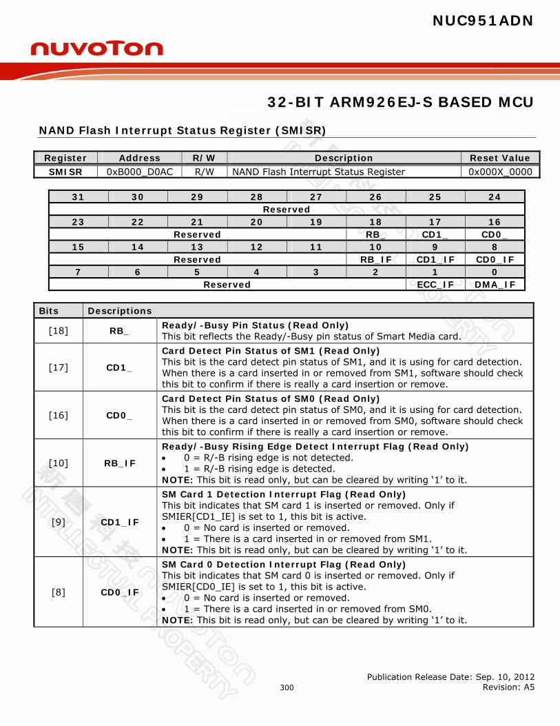
NUC951ADN
32-BIT ARM926EJ-S BASED MCU
Publication Release Date: Sep. 10, 2012 Revision: A5
300
NAND Flash Interrupt Status Register (SMISR)
Register Address R/W Description Reset Value SMISR 0xB000_D0AC R/W NAND Flash Interrupt Status Register 0x000X_0000
31 30 29 28 27 26 25 24
Reserved 23 22 21 20 19 18 17 16
Reserved RB_ CD1_ CD0_ 15 14 13 12 11 10 9 8
Reserved RB_IF CD1_IF CD0_IF 7 6 5 4 3 2 1 0
Reserved ECC_IF DMA_IF Bits Descriptions
[18] RB_ Ready/-Busy Pin Status (Read Only) This bit reflects the Ready/-Busy pin status of Smart Media card.
[17] CD1_
Card Detect Pin Status of SM1 (Read Only) This bit is the card detect pin status of SM1, and it is using for card detection. When there is a card inserted in or removed from SM1, software should check this bit to confirm if there is really a card insertion or remove.
[16] CD0_
Card Detect Pin Status of SM0 (Read Only) This bit is the card detect pin status of SM0, and it is using for card detection. When there is a card inserted in or removed from SM0, software should check this bit to confirm if there is really a card insertion or remove.
[10] RB_IF
Ready/-Busy Rising Edge Detect Interrupt Flag (Read Only) 0 = R/-B rising edge is not detected. 1 = R/-B rising edge is detected. NOTE: This bit is read only, but can be cleared by writing ‘1’ to it.
[9] CD1_IF
SM Card 1 Detection Interrupt Flag (Read Only) This bit indicates that SM card 1 is inserted or removed. Only if SMIER[CD1_IE] is set to 1, this bit is active. 0 = No card is inserted or removed. 1 = There is a card inserted in or removed from SM1. NOTE: This bit is read only, but can be cleared by writing ‘1’ to it.
[8] CD0_IF
SM Card 0 Detection Interrupt Flag (Read Only) This bit indicates that SM card 0 is inserted or removed. Only if SMIER[CD0_IE] is set to 1, this bit is active. 0 = No card is inserted or removed. 1 = There is a card inserted in or removed from SM0. NOTE: This bit is read only, but can be cleared by writing ‘1’ to it.
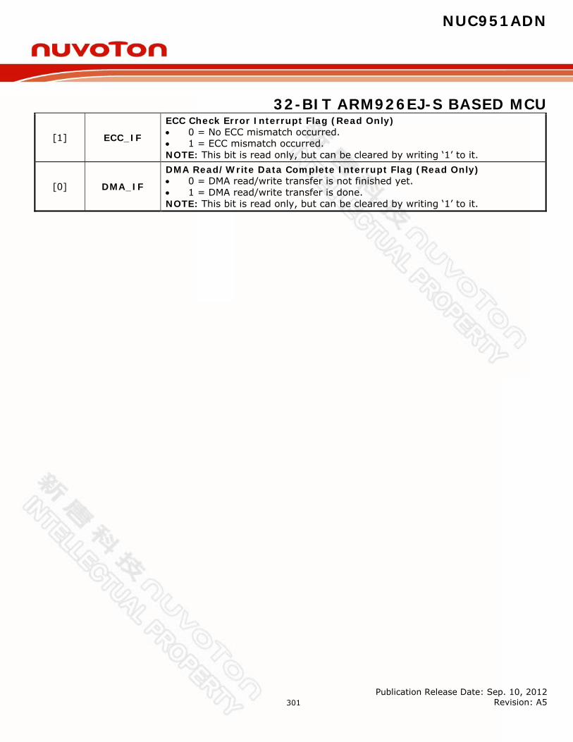
NUC951ADN
32-BIT ARM926EJ-S BASED MCU
Publication Release Date: Sep. 10, 2012 Revision: A5
301
[1] ECC_IF
ECC Check Error Interrupt Flag (Read Only) 0 = No ECC mismatch occurred. 1 = ECC mismatch occurred. NOTE: This bit is read only, but can be cleared by writing ‘1’ to it.
[0] DMA_IF
DMA Read/Write Data Complete Interrupt Flag (Read Only) 0 = DMA read/write transfer is not finished yet. 1 = DMA read/write transfer is done. NOTE: This bit is read only, but can be cleared by writing ‘1’ to it.

NUC951ADN
32-BIT ARM926EJ-S BASED MCU
Publication Release Date: Sep. 10, 2012 Revision: A5
302
NAND Flash Command Port Register (SMCMD)
Register Address R/W Description Reset Value SMCMD 0xB000_D0B0 W NAND Flash Command Port Register Undefined
31 30 29 28 27 26 25 24
Reserved 23 22 21 20 19 18 17 16
Reserved 15 14 13 12 11 10 9 8
Reserved 7 6 5 4 3 2 1 0
SMCMD Bits Descriptions
[7:0] SMCMD NAND Flash Command Port When CPU writes this port, SM H/W circuit will send a command to NAND Flash.
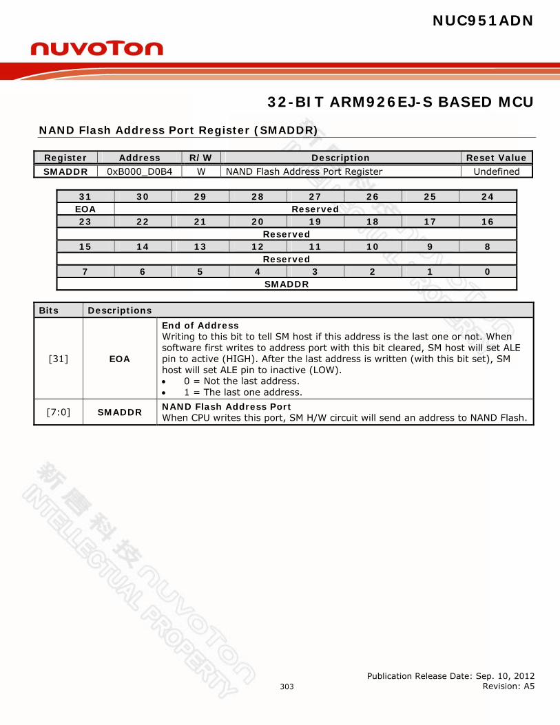
NUC951ADN
32-BIT ARM926EJ-S BASED MCU
Publication Release Date: Sep. 10, 2012 Revision: A5
303
NAND Flash Address Port Register (SMADDR)
Register Address R/W Description Reset Value SMADDR 0xB000_D0B4 W NAND Flash Address Port Register Undefined
31 30 29 28 27 26 25 24
EOA Reserved 23 22 21 20 19 18 17 16
Reserved 15 14 13 12 11 10 9 8
Reserved 7 6 5 4 3 2 1 0
SMADDR Bits Descriptions
[31] EOA
End of Address Writing to this bit to tell SM host if this address is the last one or not. When software first writes to address port with this bit cleared, SM host will set ALE pin to active (HIGH). After the last address is written (with this bit set), SM host will set ALE pin to inactive (LOW). 0 = Not the last address. 1 = The last one address.
[7:0] SMADDR NAND Flash Address Port When CPU writes this port, SM H/W circuit will send an address to NAND Flash.
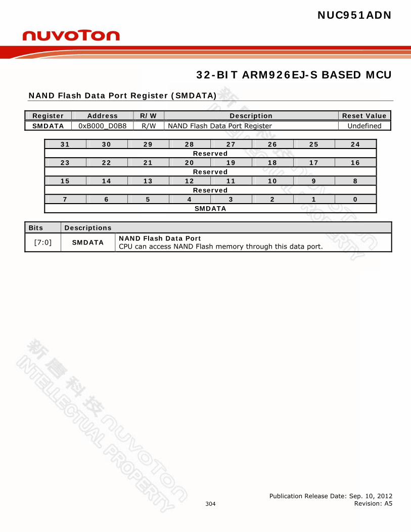
NUC951ADN
32-BIT ARM926EJ-S BASED MCU
Publication Release Date: Sep. 10, 2012 Revision: A5
304
NAND Flash Data Port Register (SMDATA)
Register Address R/W Description Reset Value SMDATA 0xB000_D0B8 R/W NAND Flash Data Port Register Undefined
31 30 29 28 27 26 25 24
Reserved 23 22 21 20 19 18 17 16
Reserved 15 14 13 12 11 10 9 8
Reserved 7 6 5 4 3 2 1 0
SMDATA Bits Descriptions
[7:0] SMDATA NAND Flash Data Port CPU can access NAND Flash memory through this data port.
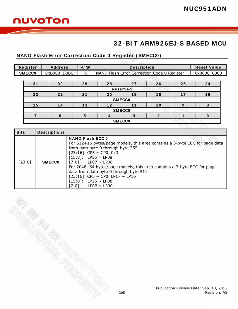
NUC951ADN
32-BIT ARM926EJ-S BASED MCU
Publication Release Date: Sep. 10, 2012 Revision: A5
305
NAND Flash Error Correction Code 0 Register (SMECC0)
Register Address R/W Description Reset Value SMECC0 0xB000_D0BC R NAND Flash Error Correction Code 0 Register 0x0000_0000
31 30 29 28 27 26 25 24
Reserved 23 22 21 20 19 18 17 16
SMECC0 15 14 13 12 11 10 9 8
SMECC0 7 6 5 4 3 2 1 0
SMECC0 Bits Descriptions
[23:0] SMECC0
NAND Flash ECC 0 For 512+16 bytes/page models, this area contains a 3-byte ECC for page data from data byte 0 through byte 255. [23:16]: CP5 ~ CP0, 0x3 [15:8]: LP15 ~ LP08 [7:0]: LP07 ~ LP00 For 2048+64 bytes/page models, this area contains a 3-byte ECC for page data from data byte 0 through byte 511. [23:16]: CP5 ~ CP0, LP17 ~ LP16 [15:8]: LP15 ~ LP08 [7:0]: LP07 ~ LP00

NUC951ADN
32-BIT ARM926EJ-S BASED MCU
Publication Release Date: Sep. 10, 2012 Revision: A5
306
NAND Flash Error Correction Code 1 Register (SMECC1)
Register Address R/W Description Reset Value SMECC1 0xB000_D0C0 R NAND Flash Error Correction Code 1 Register 0x0000_0000
31 30 29 28 27 26 25 24
Reserved 23 22 21 20 19 18 17 16
SMECC1 15 14 13 12 11 10 9 8
SMECC1 7 6 5 4 3 2 1 0
SMECC1 Bits Descriptions
[23:0] SMECC1
NAND Flash ECC 1 For 512+16 bytes/page models, this area contains a 3-byte ECC for page data from data byte 256 through byte 511. [23:16]: CP5 ~ CP0, 0x3 [15:8]: LP15 ~ LP08 [7:0]: LP07 ~ LP00 For 2048+64 bytes/page models, this area contains a 3-byte ECC for page data from data byte 512 through byte 1023. [23:16]: CP5 ~ CP0, LP17 ~ LP16 [15:8]: LP15 ~ LP08 [7:0]: LP07 ~ LP00
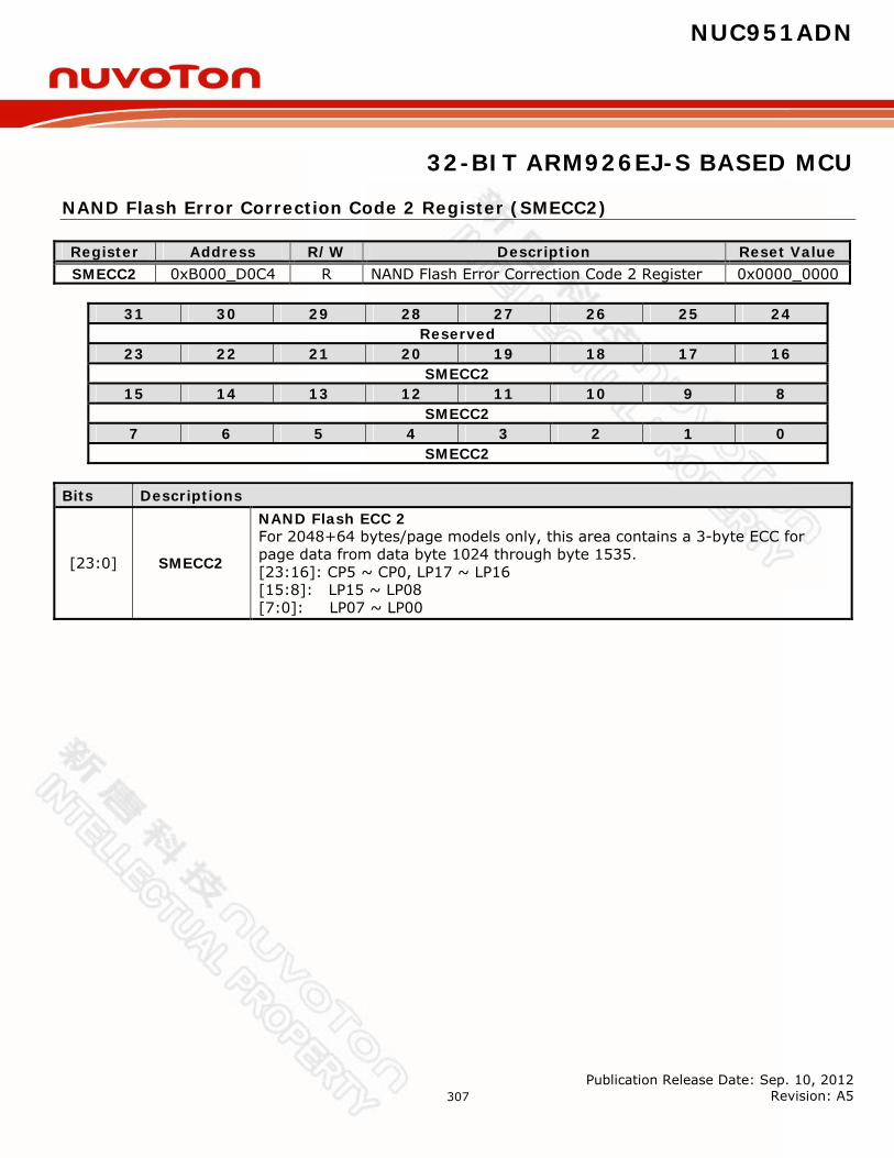
NUC951ADN
32-BIT ARM926EJ-S BASED MCU
Publication Release Date: Sep. 10, 2012 Revision: A5
307
NAND Flash Error Correction Code 2 Register (SMECC2)
Register Address R/W Description Reset Value SMECC2 0xB000_D0C4 R NAND Flash Error Correction Code 2 Register 0x0000_0000
31 30 29 28 27 26 25 24
Reserved 23 22 21 20 19 18 17 16
SMECC2 15 14 13 12 11 10 9 8
SMECC2 7 6 5 4 3 2 1 0
SMECC2 Bits Descriptions
[23:0] SMECC2
NAND Flash ECC 2 For 2048+64 bytes/page models only, this area contains a 3-byte ECC for page data from data byte 1024 through byte 1535. [23:16]: CP5 ~ CP0, LP17 ~ LP16 [15:8]: LP15 ~ LP08 [7:0]: LP07 ~ LP00

NUC951ADN
32-BIT ARM926EJ-S BASED MCU
Publication Release Date: Sep. 10, 2012 Revision: A5
308
NAND Flash Error Correction Code 3 Register (SMECC3)
Register Address R/W Description Reset Value SMECC3 0xB000_D0C8 R NAND Flash Error Correction Code 3 Register 0x0000_0000
31 30 29 28 27 26 25 24
Reserved 23 22 21 20 19 18 17 16
SMECC3 15 14 13 12 11 10 9 8
SMECC3 7 6 5 4 3 2 1 0
SMECC3 Bits Descriptions
[23:0] SMECC3
NAND Flash ECC 3 For 2048+64 bytes/page models only, this area contains a 3-byte ECC for page data from data byte 1536 through byte 2047. [23:16]: CP5 ~ CP0, LP17 ~ LP16 [15:8]: LP15 ~ LP08 [7:0]: LP07 ~ LP00
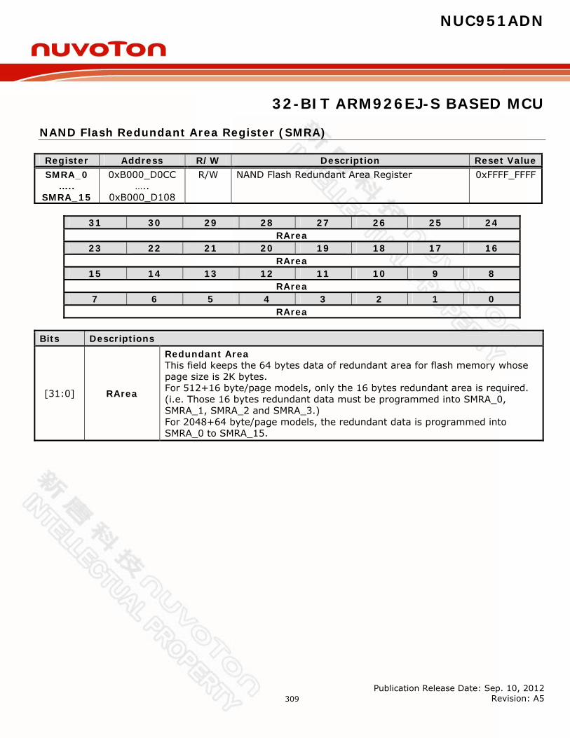
NUC951ADN
32-BIT ARM926EJ-S BASED MCU
Publication Release Date: Sep. 10, 2012 Revision: A5
309
NAND Flash Redundant Area Register (SMRA)
Register Address R/W Description Reset Value SMRA_0
….. SMRA_15
0xB000_D0CC …..
0xB000_D108
R/W NAND Flash Redundant Area Register 0xFFFF_FFFF
31 30 29 28 27 26 25 24
RArea 23 22 21 20 19 18 17 16
RArea 15 14 13 12 11 10 9 8
RArea 7 6 5 4 3 2 1 0
RArea Bits Descriptions
[31:0] RArea
Redundant Area This field keeps the 64 bytes data of redundant area for flash memory whose page size is 2K bytes. For 512+16 byte/page models, only the 16 bytes redundant area is required. (i.e. Those 16 bytes redundant data must be programmed into SMRA_0, SMRA_1, SMRA_2 and SMRA_3.) For 2048+64 byte/page models, the redundant data is programmed into SMRA_0 to SMRA_15.
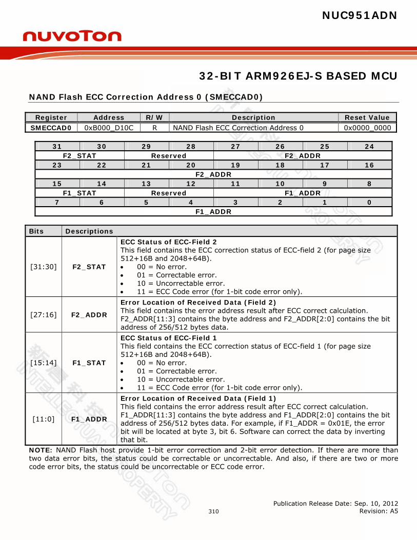
NUC951ADN
32-BIT ARM926EJ-S BASED MCU
Publication Release Date: Sep. 10, 2012 Revision: A5
310
NAND Flash ECC Correction Address 0 (SMECCAD0)
Register Address R/W Description Reset Value SMECCAD0 0xB000_D10C R NAND Flash ECC Correction Address 0 0x0000_0000
31 30 29 28 27 26 25 24 F2_STAT Reserved F2_ADDR
23 22 21 20 19 18 17 16 F2_ADDR
15 14 13 12 11 10 9 8 F1_STAT Reserved F1_ADDR
7 6 5 4 3 2 1 0 F1_ADDR
Bits Descriptions
[31:30] F2_STAT
ECC Status of ECC-Field 2 This field contains the ECC correction status of ECC-field 2 (for page size 512+16B and 2048+64B). 00 = No error. 01 = Correctable error. 10 = Uncorrectable error. 11 = ECC Code error (for 1-bit code error only).
[27:16] F2_ADDR
Error Location of Received Data (Field 2) This field contains the error address result after ECC correct calculation. F2_ADDR[11:3] contains the byte address and F2_ADDR[2:0] contains the bit address of 256/512 bytes data.
[15:14] F1_STAT
ECC Status of ECC-Field 1 This field contains the ECC correction status of ECC-field 1 (for page size 512+16B and 2048+64B). 00 = No error. 01 = Correctable error. 10 = Uncorrectable error. 11 = ECC Code error (for 1-bit code error only).
[11:0] F1_ADDR
Error Location of Received Data (Field 1) This field contains the error address result after ECC correct calculation. F1_ADDR[11:3] contains the byte address and F1_ADDR[2:0] contains the bit address of 256/512 bytes data. For example, if F1_ADDR = 0x01E, the error bit will be located at byte 3, bit 6. Software can correct the data by inverting that bit.
NOTE: NAND Flash host provide 1-bit error correction and 2-bit error detection. If there are more than two data error bits, the status could be correctable or uncorrectable. And also, if there are two or more code error bits, the status could be uncorrectable or ECC code error.
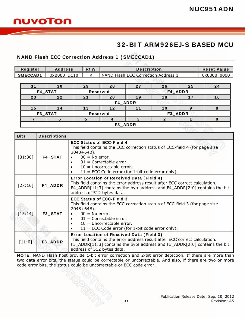
NUC951ADN
32-BIT ARM926EJ-S BASED MCU
Publication Release Date: Sep. 10, 2012 Revision: A5
311
NAND Flash ECC Correction Address 1 (SMECCAD1)
Register Address R/W Description Reset Value SMECCAD1 0xB000_D110 R NAND Flash ECC Correction Address 1 0x0000_0000
31 30 29 28 27 26 25 24 F4_STAT Reserved F4_ADDR
23 22 21 20 19 18 17 16 F4_ADDR
15 14 13 12 11 10 9 8 F3_STAT Reserved F3_ADDR
7 6 5 4 3 2 1 0 F3_ADDR
Bits Descriptions
[31:30] F4_STAT
ECC Status of ECC-Field 4 This field contains the ECC correction status of ECC-field 4 (for page size 2048+64B). 00 = No error. 01 = Correctable error. 10 = Uncorrectable error. 11 = ECC Code error (for 1-bit code error only).
[27:16] F4_ADDR
Error Location of Received Data (Field 4) This field contains the error address result after ECC correct calculation. F4_ADDR[11:3] contains the byte address and F4_ADDR[2:0] contains the bit address of 512 bytes data.
[15:14] F3_STAT
ECC Status of ECC-Field 3 This field contains the ECC correction status of ECC-field 3 (for page size 2048+64B). 00 = No error. 01 = Correctable error. 10 = Uncorrectable error. 11 = ECC Code error (for 1-bit code error only).
[11:0] F3_ADDR
Error Location of Received Data (Field 3) This field contains the error address result after ECC correct calculation. F3_ADDR[11:3] contains the byte address and F3_ADDR[2:0] contains the bit address of 512 bytes data.
NOTE: NAND Flash host provide 1-bit error correction and 2-bit error detection. If there are more than two data error bits, the status could be correctable or uncorrectable. And also, if there are two or more code error bits, the status could be uncorrectable or ECC code error.
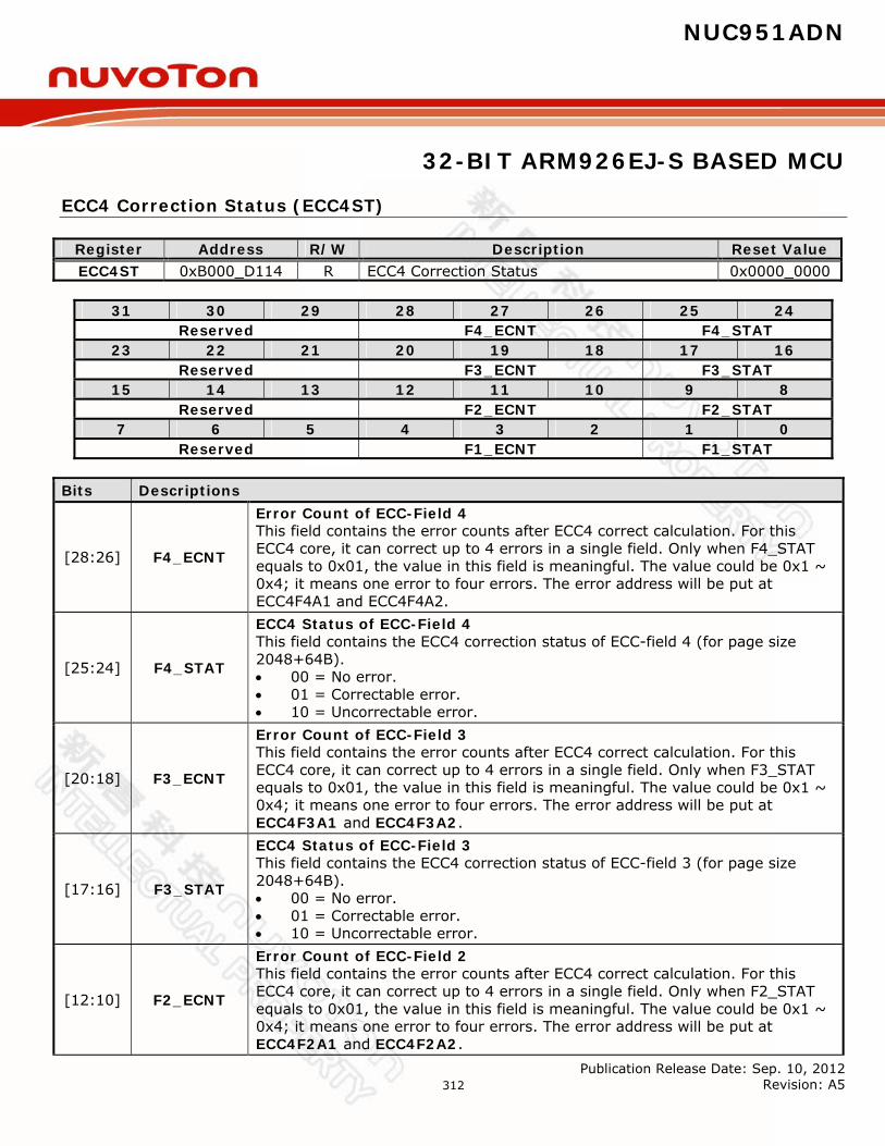
NUC951ADN
32-BIT ARM926EJ-S BASED MCU
Publication Release Date: Sep. 10, 2012 Revision: A5
312
ECC4 Correction Status (ECC4ST)
Register Address R/W Description Reset Value ECC4ST 0xB000_D114 R ECC4 Correction Status 0x0000_0000
31 30 29 28 27 26 25 24
Reserved F4_ECNT F4_STAT 23 22 21 20 19 18 17 16
Reserved F3_ECNT F3_STAT 15 14 13 12 11 10 9 8
Reserved F2_ECNT F2_STAT 7 6 5 4 3 2 1 0
Reserved F1_ECNT F1_STAT Bits Descriptions
[28:26] F4_ECNT
Error Count of ECC-Field 4 This field contains the error counts after ECC4 correct calculation. For this ECC4 core, it can correct up to 4 errors in a single field. Only when F4_STAT equals to 0x01, the value in this field is meaningful. The value could be 0x1 ~ 0x4; it means one error to four errors. The error address will be put at ECC4F4A1 and ECC4F4A2.
[25:24] F4_STAT
ECC4 Status of ECC-Field 4 This field contains the ECC4 correction status of ECC-field 4 (for page size 2048+64B). 00 = No error. 01 = Correctable error. 10 = Uncorrectable error.
[20:18] F3_ECNT
Error Count of ECC-Field 3 This field contains the error counts after ECC4 correct calculation. For this ECC4 core, it can correct up to 4 errors in a single field. Only when F3_STAT equals to 0x01, the value in this field is meaningful. The value could be 0x1 ~ 0x4; it means one error to four errors. The error address will be put at ECC4F3A1 and ECC4F3A2.
[17:16] F3_STAT
ECC4 Status of ECC-Field 3 This field contains the ECC4 correction status of ECC-field 3 (for page size 2048+64B). 00 = No error. 01 = Correctable error. 10 = Uncorrectable error.
[12:10] F2_ECNT
Error Count of ECC-Field 2 This field contains the error counts after ECC4 correct calculation. For this ECC4 core, it can correct up to 4 errors in a single field. Only when F2_STAT equals to 0x01, the value in this field is meaningful. The value could be 0x1 ~ 0x4; it means one error to four errors. The error address will be put at ECC4F2A1 and ECC4F2A2.
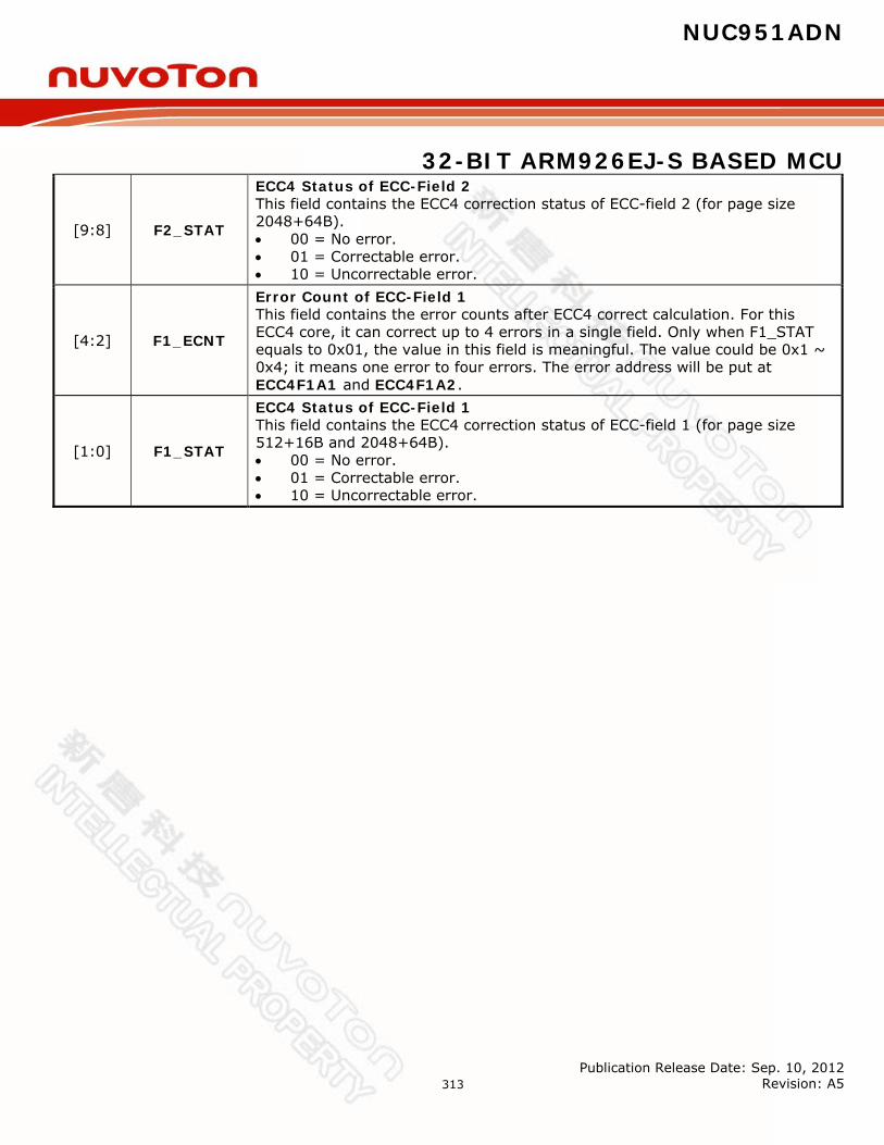
NUC951ADN
32-BIT ARM926EJ-S BASED MCU
Publication Release Date: Sep. 10, 2012 Revision: A5
313
[9:8] F2_STAT
ECC4 Status of ECC-Field 2 This field contains the ECC4 correction status of ECC-field 2 (for page size 2048+64B). 00 = No error. 01 = Correctable error. 10 = Uncorrectable error.
[4:2] F1_ECNT
Error Count of ECC-Field 1 This field contains the error counts after ECC4 correct calculation. For this ECC4 core, it can correct up to 4 errors in a single field. Only when F1_STAT equals to 0x01, the value in this field is meaningful. The value could be 0x1 ~ 0x4; it means one error to four errors. The error address will be put at ECC4F1A1 and ECC4F1A2.
[1:0] F1_STAT
ECC4 Status of ECC-Field 1 This field contains the ECC4 correction status of ECC-field 1 (for page size 512+16B and 2048+64B). 00 = No error. 01 = Correctable error. 10 = Uncorrectable error.
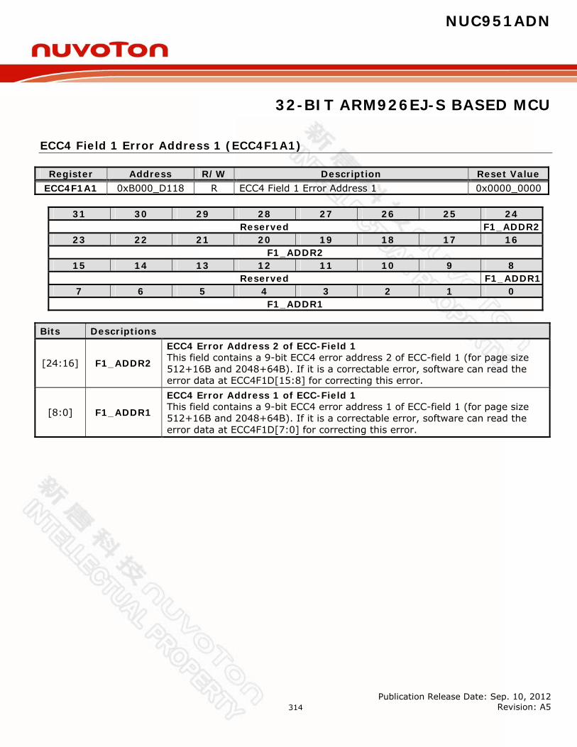
NUC951ADN
32-BIT ARM926EJ-S BASED MCU
Publication Release Date: Sep. 10, 2012 Revision: A5
314
ECC4 Field 1 Error Address 1 (ECC4F1A1)
Register Address R/W Description Reset Value ECC4F1A1 0xB000_D118 R ECC4 Field 1 Error Address 1 0x0000_0000
31 30 29 28 27 26 25 24
Reserved F1_ADDR2 23 22 21 20 19 18 17 16
F1_ADDR2 15 14 13 12 11 10 9 8
Reserved F1_ADDR1 7 6 5 4 3 2 1 0
F1_ADDR1 Bits Descriptions
[24:16] F1_ADDR2
ECC4 Error Address 2 of ECC-Field 1 This field contains a 9-bit ECC4 error address 2 of ECC-field 1 (for page size 512+16B and 2048+64B). If it is a correctable error, software can read the error data at ECC4F1D[15:8] for correcting this error.
[8:0] F1_ADDR1
ECC4 Error Address 1 of ECC-Field 1 This field contains a 9-bit ECC4 error address 1 of ECC-field 1 (for page size 512+16B and 2048+64B). If it is a correctable error, software can read the error data at ECC4F1D[7:0] for correcting this error.

NUC951ADN
32-BIT ARM926EJ-S BASED MCU
Publication Release Date: Sep. 10, 2012 Revision: A5
315
ECC4 Field 1 Error Address 2 (ECC4F1A2)
Register Address R/W Description Reset Value ECC4F1A2 0xB000_D11C R ECC4 Field 1 Error Address 2 0x0000_0000
31 30 29 28 27 26 25 24
Reserved F1_ADDR4 23 22 21 20 19 18 17 16
F1_ADDR4 15 14 13 12 11 10 9 8
Reserved F1_ADDR3 7 6 5 4 3 2 1 0
F1_ADDR3 Bits Descriptions
[24:16] F1_ADDR4
ECC4 Error Address 4 of ECC-Field 1 This field contains a 9-bit ECC4 error address 4 of ECC-field 1 (for page size 512+16B and 2048+64B). If it is a correctable error, software can read the error data at ECC4F1D[31:24] for correcting this error.
[8:0] F1_ADDR3
ECC4 Error Address 3 of ECC-Field 1 This field contains a 9-bit ECC4 error address 3 of ECC-field 1 (for page size 512+16B and 2048+64B). If it is a correctable error, software can read the error data at ECC4F1D[23:16] for correcting this error.
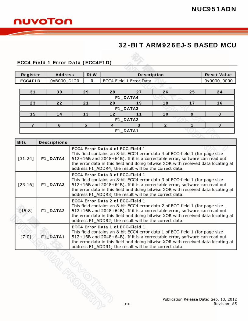
NUC951ADN
32-BIT ARM926EJ-S BASED MCU
Publication Release Date: Sep. 10, 2012 Revision: A5
316
ECC4 Field 1 Error Data (ECC4F1D)
Register Address R/W Description Reset Value ECC4F1D 0xB000_D120 R ECC4 Field 1 Error Data 0x0000_0000
31 30 29 28 27 26 25 24
F1_DATA4 23 22 21 20 19 18 17 16
F1_DATA3 15 14 13 12 11 10 9 8
F1_DATA2 7 6 5 4 3 2 1 0
F1_DATA1 Bits Descriptions
[31:24] F1_DATA4
ECC4 Error Data 4 of ECC-Field 1 This field contains an 8-bit ECC4 error data 4 of ECC-field 1 (for page size 512+16B and 2048+64B). If it is a correctable error, software can read out the error data in this field and doing bitwise XOR with received data locating at address F1_ADDR4; the result will be the correct data.
[23:16] F1_DATA3
ECC4 Error Data 3 of ECC-Field 1 This field contains an 8-bit ECC4 error data 3 of ECC-field 1 (for page size 512+16B and 2048+64B). If it is a correctable error, software can read out the error data in this field and doing bitwise XOR with received data locating at address F1_ADDR3; the result will be the correct data.
[15:8] F1_DATA2
ECC4 Error Data 2 of ECC-Field 1 This field contains an 8-bit ECC4 error data 2 of ECC-field 1 (for page size 512+16B and 2048+64B). If it is a correctable error, software can read out the error data in this field and doing bitwise XOR with received data locating at address F1_ADDR2; the result will be the correct data.
[7:0] F1_DATA1
ECC4 Error Data 1 of ECC-Field 1 This field contains an 8-bit ECC4 error data 1 of ECC-field 1 (for page size 512+16B and 2048+64B). If it is a correctable error, software can read out the error data in this field and doing bitwise XOR with received data locating at address F1_ADDR1; the result will be the correct data.

NUC951ADN
32-BIT ARM926EJ-S BASED MCU
Publication Release Date: Sep. 10, 2012 Revision: A5
317
ECC4 Field 2 Error Address 1 (ECC4F2A1)
Register Address R/W Description Reset Value ECC4F2A1 0xB000_D124 R ECC4 Field 2 Error Address 1 0x0000_0000
31 30 29 28 27 26 25 24
Reserved F2_ADDR2 23 22 21 20 19 18 17 16
F2_ADDR2 15 14 13 12 11 10 9 8
Reserved F2_ADDR1 7 6 5 4 3 2 1 0
F2_ADDR1 Bits Descriptions
[24:16] F2_ADDR2
ECC4 Error Address 2 of ECC-Field 2 This field contains a 9-bit ECC4 error address 2 of ECC-field 2 (for page size 2048+64B). If it is a correctable error, software can read the error data at ECC4F2D[15:8] for correcting this error.
[8:0] F2_ADDR1
ECC4 Error Address 1 of ECC-Field 2 This field contains a 9-bit ECC4 error address 1 of ECC-field 2 (for page size 2048+64B). If it is a correctable error, software can read the error data at ECC4F2D[7:0] for correcting this error.
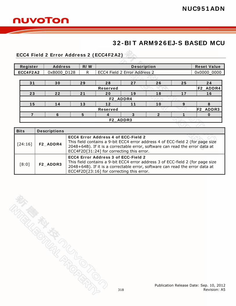
NUC951ADN
32-BIT ARM926EJ-S BASED MCU
Publication Release Date: Sep. 10, 2012 Revision: A5
318
ECC4 Field 2 Error Address 2 (ECC4F2A2)
Register Address R/W Description Reset Value ECC4F2A2 0xB000_D128 R ECC4 Field 2 Error Address 2 0x0000_0000
31 30 29 28 27 26 25 24
Reserved F2_ADDR4 23 22 21 20 19 18 17 16
F2_ADDR4 15 14 13 12 11 10 9 8
Reserved F2_ADDR3 7 6 5 4 3 2 1 0
F2_ADDR3 Bits Descriptions
[24:16] F2_ADDR4
ECC4 Error Address 4 of ECC-Field 2 This field contains a 9-bit ECC4 error address 4 of ECC-field 2 (for page size 2048+64B). If it is a correctable error, software can read the error data at ECC4F2D[31:24] for correcting this error.
[8:0] F2_ADDR3
ECC4 Error Address 3 of ECC-Field 2 This field contains a 9-bit ECC4 error address 3 of ECC-field 2 (for page size 2048+64B). If it is a correctable error, software can read the error data at ECC4F2D[23:16] for correcting this error.

NUC951ADN
32-BIT ARM926EJ-S BASED MCU
Publication Release Date: Sep. 10, 2012 Revision: A5
319
ECC4 Field 2 Error Data (ECC4F2D)
Register Address R/W Description Reset Value ECC4F2D 0xB000_D12C R ECC4 Field 2 Error Data 0x0000_0000
31 30 29 28 27 26 25 24
F2_DATA4 23 22 21 20 19 18 17 16
F2_DATA3 15 14 13 12 11 10 9 8
F2_DATA2 7 6 5 4 3 2 1 0
F2_DATA1 Bits Descriptions
[31:24] F2_DATA4
ECC4 Error Data 4 of ECC-Field 2 This field contains an 8-bit ECC4 error data 4 of ECC-field 2 (for page size 2048+64B). If it is a correctable error, software can read out the error data in this field and doing bitwise XOR with received data locating at address F2_ADDR4; the result will be the correct data.
[23:16] F2_DATA3
ECC4 Error Data 3 of ECC-Field 2 This field contains an 8-bit ECC4 error data 3 of ECC-field 2 (for page size 2048+64B). If it is a correctable error, software can read out the error data in this field and doing bitwise XOR with received data locating at address F2_ADDR3; the result will be the correct data.
[15:8] F2_DATA2
ECC4 Error Data 2 of ECC-Field 2 This field contains an 8-bit ECC4 error data 2 of ECC-field 2 (for page size 2048+64B). If it is a correctable error, software can read out the error data in this field and doing bitwise XOR with received data locating at address F2_ADDR2; the result will be the correct data.
[7:0] F2_DATA1
ECC4 Error Data 1 of ECC-Field 2 This field contains an 8-bit ECC4 error data 1 of ECC-field 2 (for page size 2048+64B). If it is a correctable error, software can read out the error data in this field and doing bitwise XOR with received data locating at address F2_ADDR1; the result will be the correct data.

NUC951ADN
32-BIT ARM926EJ-S BASED MCU
Publication Release Date: Sep. 10, 2012 Revision: A5
320
ECC4 Field 3 Error Address 1 (ECC4F3A1)
Register Address R/W Description Reset Value ECC4F3A1 0xB000_D130 R ECC4 Field 3 Error Address 1 0x0000_0000
31 30 29 28 27 26 25 24
Reserved F3_ADDR2 23 22 21 20 19 18 17 16
F3_ADDR2 15 14 13 12 11 10 9 8
Reserved F3_ADDR1 7 6 5 4 3 2 1 0
F3_ADDR1 Bits Descriptions
[24:16] F3_ADDR2
ECC4 Error Address 2 of ECC-Field 3 This field contains a 9-bit ECC4 error address 2 of ECC-field 3 (for page size 2048+64B). If it is a correctable error, software can read the error data at ECC4F3D[15:8] for correcting this error.
[8:0] F3_ADDR1
ECC4 Error Address 1 of ECC-Field 3 This field contains a 9-bit ECC4 error address 1 of ECC-field 3 (for page size 2048+64B). If it is a correctable error, software can read the error data at ECC4F3D[7:0] for correcting this error.
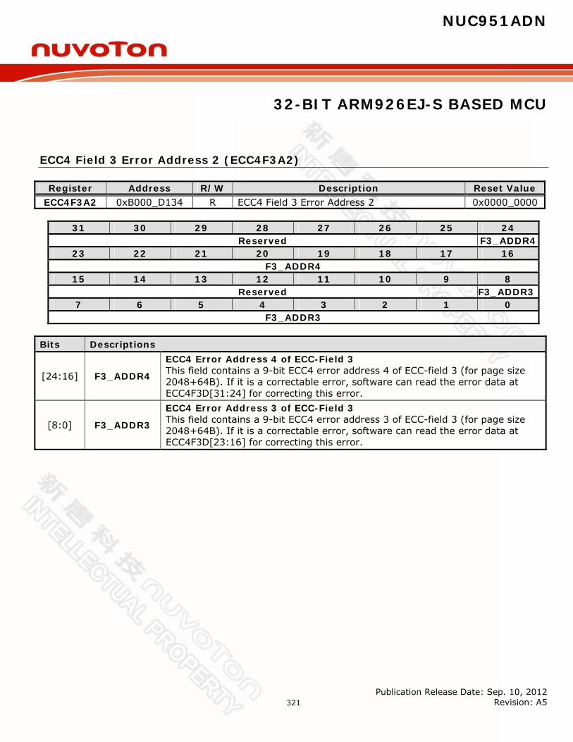
NUC951ADN
32-BIT ARM926EJ-S BASED MCU
Publication Release Date: Sep. 10, 2012 Revision: A5
321
ECC4 Field 3 Error Address 2 (ECC4F3A2)
Register Address R/W Description Reset Value ECC4F3A2 0xB000_D134 R ECC4 Field 3 Error Address 2 0x0000_0000
31 30 29 28 27 26 25 24
Reserved F3_ADDR4 23 22 21 20 19 18 17 16
F3_ADDR4 15 14 13 12 11 10 9 8
Reserved F3_ADDR3 7 6 5 4 3 2 1 0
F3_ADDR3 Bits Descriptions
[24:16] F3_ADDR4
ECC4 Error Address 4 of ECC-Field 3 This field contains a 9-bit ECC4 error address 4 of ECC-field 3 (for page size 2048+64B). If it is a correctable error, software can read the error data at ECC4F3D[31:24] for correcting this error.
[8:0] F3_ADDR3
ECC4 Error Address 3 of ECC-Field 3 This field contains a 9-bit ECC4 error address 3 of ECC-field 3 (for page size 2048+64B). If it is a correctable error, software can read the error data at ECC4F3D[23:16] for correcting this error.

NUC951ADN
32-BIT ARM926EJ-S BASED MCU
Publication Release Date: Sep. 10, 2012 Revision: A5
322
ECC4 Field 3 Error Data (ECC4F3D)
Register Address R/W Description Reset Value ECC4F3D 0xB000_D138 R ECC4 Field 3 Error Data 0x0000_0000
31 30 29 28 27 26 25 24
F3_DATA4 23 22 21 20 19 18 17 16
F3_DATA3 15 14 13 12 11 10 9 8
F3_DATA2 7 6 5 4 3 2 1 0
F3_DATA1 Bits Descriptions
[31:24] F3_DATA4
ECC4 Error Data 4 of ECC-Field 3 This field contains an 8-bit ECC4 error data 4 of ECC-field 3 (for page size 2048+64B). If it is a correctable error, software can read out the error data in this field and doing bitwise XOR with received data locating at address F3_ADDR4; the result will be the correct data.
[23:16] F3_DATA3
ECC4 Error Data 3 of ECC-Field 3 This field contains an 8-bit ECC4 error data 3 of ECC-field 3 (for page size 2048+64B). If it is a correctable error, software can read out the error data in this field and doing bitwise XOR with received data locating at address F3_ADDR3; the result will be the correct data.
[15:8] F3_DATA2
ECC4 Error Data 2 of ECC-Field 3 This field contains an 8-bit ECC4 error data 2 of ECC-field 3 (for page size 2048+64B). If it is a correctable error, software can read out the error data in this field and doing bitwise XOR with received data locating at address F3_ADDR2; the result will be the correct data.
[7:0] F3_DATA1
ECC4 Error Data 1 of ECC-Field 3 This field contains an 8-bit ECC4 error data 1 of ECC-field 3 (for page size 2048+64B). If it is a correctable error, software can read out the error data in this field and doing bitwise XOR with received data locating at address F3_ADDR1; the result will be the correct data.
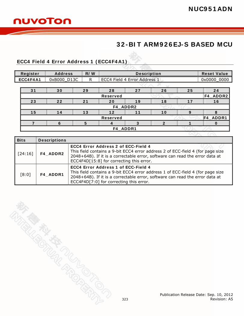
NUC951ADN
32-BIT ARM926EJ-S BASED MCU
Publication Release Date: Sep. 10, 2012 Revision: A5
323
ECC4 Field 4 Error Address 1 (ECC4F4A1)
Register Address R/W Description Reset Value ECC4F4A1 0xB000_D13C R ECC4 Field 4 Error Address 1 0x0000_0000
31 30 29 28 27 26 25 24
Reserved F4_ADDR2 23 22 21 20 19 18 17 16
F4_ADDR2 15 14 13 12 11 10 9 8
Reserved F4_ADDR1 7 6 5 4 3 2 1 0
F4_ADDR1 Bits Descriptions
[24:16] F4_ADDR2
ECC4 Error Address 2 of ECC-Field 4 This field contains a 9-bit ECC4 error address 2 of ECC-field 4 (for page size 2048+64B). If it is a correctable error, software can read the error data at ECC4F4D[15:8] for correcting this error.
[8:0] F4_ADDR1
ECC4 Error Address 1 of ECC-Field 4 This field contains a 9-bit ECC4 error address 1 of ECC-field 4 (for page size 2048+64B). If it is a correctable error, software can read the error data at ECC4F4D[7:0] for correcting this error.

NUC951ADN
32-BIT ARM926EJ-S BASED MCU
Publication Release Date: Sep. 10, 2012 Revision: A5
324
ECC4 Field 4 Error Address 2 (ECC4F4A2)
Register Address R/W Description Reset Value ECC4F4A2 0xB000_D140 R ECC4 Field 4 Error Address 2 0x0000_0000
31 30 29 28 27 26 25 24
Reserved F4_ADDR4 23 22 21 20 19 18 17 16
F4_ADDR4 15 14 13 12 11 10 9 8
Reserved F4_ADDR3 7 6 5 4 3 2 1 0
F4_ADDR3 Bits Descriptions
[24:16] F4_ADDR4
ECC4 Error Address 4 of ECC-Field 4 This field contains a 9-bit ECC4 error address 4 of ECC-field 4 (for page size 2048+64B). If it is a correctable error, software can read the error data at ECC4F4D[31:24] for correcting this error.
[8:0] F4_ADDR3
ECC4 Error Address 3 of ECC-Field 4 This field contains a 9-bit ECC4 error address 3 of ECC-field 4 (for page size 2048+64B). If it is a correctable error, software can read the error data at ECC4F4D[23:16] for correcting this error.
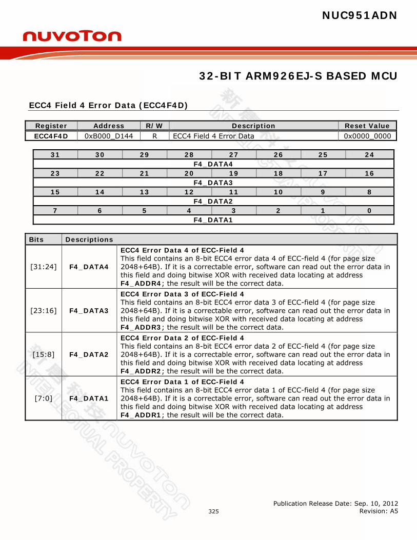
NUC951ADN
32-BIT ARM926EJ-S BASED MCU
Publication Release Date: Sep. 10, 2012 Revision: A5
325
ECC4 Field 4 Error Data (ECC4F4D)
Register Address R/W Description Reset Value ECC4F4D 0xB000_D144 R ECC4 Field 4 Error Data 0x0000_0000
31 30 29 28 27 26 25 24
F4_DATA4 23 22 21 20 19 18 17 16
F4_DATA3 15 14 13 12 11 10 9 8
F4_DATA2 7 6 5 4 3 2 1 0
F4_DATA1 Bits Descriptions
[31:24] F4_DATA4
ECC4 Error Data 4 of ECC-Field 4 This field contains an 8-bit ECC4 error data 4 of ECC-field 4 (for page size 2048+64B). If it is a correctable error, software can read out the error data in this field and doing bitwise XOR with received data locating at address F4_ADDR4; the result will be the correct data.
[23:16] F4_DATA3
ECC4 Error Data 3 of ECC-Field 4 This field contains an 8-bit ECC4 error data 3 of ECC-field 4 (for page size 2048+64B). If it is a correctable error, software can read out the error data in this field and doing bitwise XOR with received data locating at address F4_ADDR3; the result will be the correct data.
[15:8] F4_DATA2
ECC4 Error Data 2 of ECC-Field 4 This field contains an 8-bit ECC4 error data 2 of ECC-field 4 (for page size 2048+64B). If it is a correctable error, software can read out the error data in this field and doing bitwise XOR with received data locating at address F4_ADDR2; the result will be the correct data.
[7:0] F4_DATA1
ECC4 Error Data 1 of ECC-Field 4 This field contains an 8-bit ECC4 error data 1 of ECC-field 4 (for page size 2048+64B). If it is a correctable error, software can read out the error data in this field and doing bitwise XOR with received data locating at address F4_ADDR1; the result will be the correct data.
NUC951ADN
32-BIT ARM926EJ-S BASED MCU
Publication Release Date: Sep. 10, 2012 Revision: A5
326
7.11 LCD Display Interface Controller (LCM) The main purpose of Display Controller is used to display the image data to LCD device or connect with external TV-encoder. The input data format of the display controller can be packet YUV422, packet RGB444, packet RGB565, packet RGB666, and packet RGB888. The OSD (On Screen Display) function supports packet YUV422 and 8/16/24-bit direct-color mode. The LCD controller supports both sync-type and MPU-type LCM module. This LCD Controller is a bus master and can transfer display data from system memory (SDRAM) without CPU intervention. Features Input data format
YUV422, YUV444 RGB444, RGB565, RGB666, RGB888
Output format YUV422, YUV444 RGB444, RGB565, RGB666, RGB888
Display size: Maximum size 1024x600 Image resize
Horizontal up-scaling 1~8X in fractional steps Vertical up-scaling 1~8X in fractional steps
Convert RGB565, RGB888, YUV422 display data to RGB444, RGB565, RGB666, RGB888 Convert full range YUV to CCIR601 Windowing support for three OSD graphic or text overlay Support CCIR-656 (with header), CCIR-601(with hsync and vsync ) 8/16-bit YUV data output format
to connect with external TV encoder Support both sync-type and MPU-type LCM (with v-sync or not) Support the 8/9/16/18/24-bit data output to connect with 80/68 series MPU type LCM module Convert YUV422, YUV444, RGB565, RGB888, YUV444, display data to RGB444, RGB565, RGB666,
RGB888, YUV422, YUV444
The LCD Controller includes the following main functions: Image post-processing Display & overlay control Image output control Hardware cursor control
NUC951ADN
32-BIT ARM926EJ-S BASED MCU
Publication Release Date: Sep. 10, 2012 Revision: A5
327
7.11.1 LCD Controller Function Description 7.11.1.1 VPOST Processor The Display Engine is used to scale-up the image for display. The image can be arbitrarily up-scaled to full-screen size in horizontal and vertical direction by programming the scaling-factor registers VA_SCALE. Similarly, the OSD function also supports up-scaling in horizontal and vertical direction. But it only supports 2X and 4X up-scaling.
7.11.1.2 Display & Overlay Control The Display Control unit includes timing controller and overlay controller. The timing controller generates the required horizontal and vertical timing for display device. The display timing is defined in the control registers,CRTC_SIZE~CRTC_VR and OSD_WINS~OSD_WINE. The following figure specifies the registers definition.
7.11.1.3 Digital Display Output Control Various digital image output modes are supported:
(1) 8-bit/16-bit YUV output for external TV-encoder; (2) 8-bit RGB output for sync-based TFT-LCD device; (3) 8-bit/16-bit/18-bit RGB output for high-color sync-based TFT-LCD device; (4) 8-bit/9-bit/16-bit/18-bit RGB output for MPU-interfaced LCD device.
The display device is defined in register DEVICE_CTRL[DEVICE]. The data bus 8-bit/16-bit or 9-bit/18-bit is selected by DEVICE_CTRL[DBWORD]. For the MPU-interfaced LCD, 68-series and 80-series MPU interface are supported. The display color formats can be 4096 (RGB444), 65536 (RGB565), and 262144 (RGB666) colors both in 8-bit and 16-bit or 9-bit and 18-bit data bus modes. The related control signals for MPU-interfaced LCD are defined in register DEVICE_CTRL. In addition, the image source color format can be YUV or RGB by setting register DCCS[VA_SRC]. 7.11.1.4 Display Pin Assignment Pad name VD [23:0] HSYNC VSYNC VDEN VICLK VOCLK Sync mode LCD data bus(O) HSYNC(O) VSYNC(O) Data enable(O) Clock in (I) Clock out (O)
MPU80 LCD data bus(I/O) Write (WR) (O) Read (RD) (O) MPU-LCD (RS) (O) Non used Chip select(CS) (O)
MPU80+VSync LCD data bus(I/O) Write (WR) (O) Read (RD) (O) MPU-LCD (RS) (O) Vsync (O) Chip select(CS) (O)
MPU80+FMARK LCD data bus(I/O) Write (WR) (O) Read (RD) (O) MPU-LCD (RS) (O) FMARK (I) Chip select(CS) (O)
MPU68 LCD data bus(I/O) Read/Write (RW) (O) Enable (EN) (O) MPU-LCD (RS) (O) Non used Chip select(CS) (O)
MPU68+VSync LCD data bus(I/O) Read/Write (RW) (O) Enable (EN) (O) MPU-LCD (RS) (O) Vsync (O) Chip select(CS) (O)
MPU68+FMARK LCD data bus(I/O) Read/Write (RW) (O) Enable (EN) (O) MPU-LCD (RS) (O) FMARK (I) Chip select(CS) (O)

NUC951ADN
32-BIT ARM926EJ-S BASED MCU
Publication Release Date: Sep. 10, 2012 Revision: A5
328
7.11.2 LCD Controller Register Map Control and Status Registers Register Offset R/W Description Reset Value
(LCM_BA = 0xB000_8000 )
DCCS 0xB000_8000 R/W Display Controller Control/Status Register 0x0000_0000
DEVICE_CTRL 0xB000_8004 R/W Display Output Device Control Register 0x0000_00E0
MPULCD_CMD 0xB000_8008 R/W MPU-Interface LCD Write Command 0x0000_0000
INT_CS 0xB000_800C R/W Interrupt Control/Status Register 0x0000_0000
CRTC_SIZE 0xB000_8010 R/W CRTC Display Size Control Register 0x0000_0000
CRTC_DEND 0xB000_8014 R/W CRTC Display Enable End 0x0000_0000
CRTC_HR 0xB000_8018 R/W CRTC Internal Horizontal Retrace Control Register 0x0000_0000
CRTC_HSYNC 0xB000_801C R/W CRTC Horizontal Sync Control Register 0x0000_0000
CRTC_VR 0xB000_8020 R/W CRTC Internal Vertical Retrace Control Reg. 0x0000_0000
VA_BADDR0 0xB000_8024 R/W Image Stream Frame Buffer-0 Starting Address. 0x0000_0000
VA_BADDR1 0xB000_8028 R/W Image Stream Frame Buffer-1 Starting Address. 0x0000_0000
VA_FBCTRL 0xB000_802C R/W Image Stream Frame Buffer Control Register 0x0000_0000
VA_SCALE 0xB000_8030 R/W Image Stream Scaling Control Register 0x0000_0000
VA_WIN 0xB000_8038 R/W Image Stream Active Window Coordinates 0x0001_07FF
VA_STUFF 0xB000_803C R/W Image Stream Stuff Pixel 0x0000_0000
OSD_WINS 0xB000_8040 R/W OSD Window Starting Coordinates 0x0000_0000
OSD_WINE 0xB000_8044 R/W OSD Window Ending Coordinates 0x0000_0000
OSD_BADDR 0xB000_8048 R/W OSD Stream Frame Buffer Starting Address 0x0000_0000
OSD_FBCTRL 0xB000_804C R/W OSD Stream Frame Buffer Control Register 0x0000_0000
OSD_OVERLAY 0xB000_8050 R/W OSD Overlay Control Register 0x0000_0000
OSD_CKEY 0xB000_8054 R/W OSD Overlay Color-Key Pattern Register 0x0000_0000
OSD_CMASK 0xB000_8058 R/W OSD Overlay Color-Key Mask Register 0x0000_0000
OSD_SKIP1 0xB000_805C R/W OSD Window Skip1 Register 0x0000_0000
OSD_SKIP2 0xB000_8060 R/W OSD Window Skip2 Register 0x0000_0000

NUC951ADN
32-BIT ARM926EJ-S BASED MCU
Publication Release Date: Sep. 10, 2012 Revision: A5
329
OSD_SCALE 0xB000_8064 R/W OSD horizontal up scaling control register 0x0000_0000
MPU_VSYNC 0xB000_8068 R/W MPU Vsync control register 0x0000_0000
HC_CTRL 0xB000_806C R/W Hardware cursor control Register 0x0000_0000
HC_POS 0xB000_8070 R/W Hardware cursor tip point position on va picture 0x0000_0000
HC_WBCTRL 0xB000_8074 R/W Hardware Cursor Window Buffer Control Register 0x0000_0000
HC_BADDR 0xB000_8078 R/W Hardware cursor memory base address register 0x0000_0000
HC_COLOR0 0xB000_807C R/W Hardware cursor color ram register mapped to bpp = 0 0x0000_0000
HC_COLOR1 0xB000_8080 R/W Hardware cursor color ram register mapped to bpp = 1 0x0000_0000
HC_COLOR2 0xB000_8084 R/W Hardware cursor color ram register mapped to bpp = 2 0x0000_0000
HC_COLOR3 0xB000_8088 R/W Hardware cursor color ram register mapped to bpp = 3 0x0000_0000
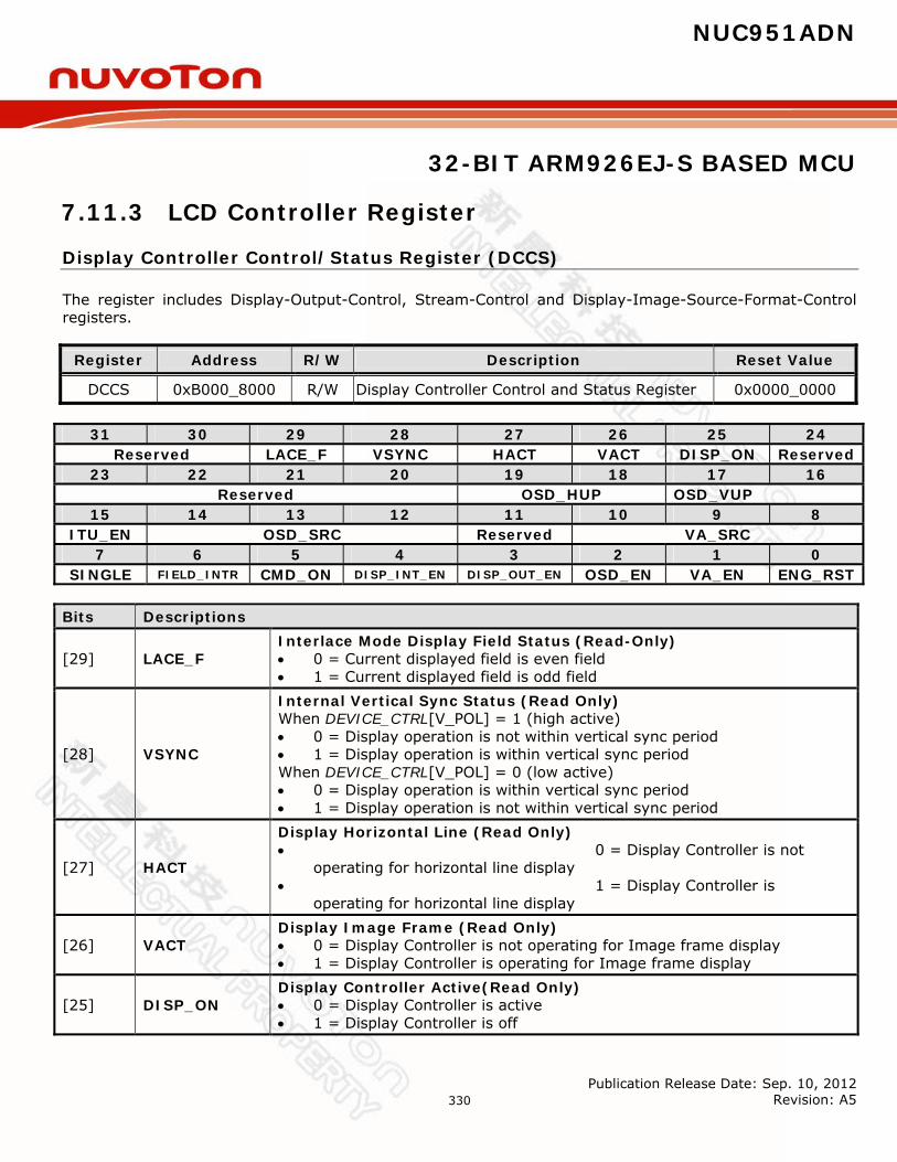
NUC951ADN
32-BIT ARM926EJ-S BASED MCU
Publication Release Date: Sep. 10, 2012 Revision: A5
330
7.11.3 LCD Controller Register
Display Controller Control/Status Register (DCCS)
The register includes Display-Output-Control, Stream-Control and Display-Image-Source-Format-Control registers.
Register Address R/W Description Reset Value
DCCS 0xB000_8000 R/W Display Controller Control and Status Register 0x0000_0000
31 30 29 28 27 26 25 24 Reserved LACE_F VSYNC HACT VACT DISP_ON Reserved
23 22 21 20 19 18 17 16 Reserved OSD_HUP OSD_VUP
15 14 13 12 11 10 9 8 ITU_EN OSD_SRC Reserved VA_SRC
7 6 5 4 3 2 1 0 SINGLE FIELD_INTR CMD_ON DISP_INT_EN DISP_OUT_EN OSD_EN VA_EN ENG_RST
Bits Descriptions
[29] LACE_F Interlace Mode Display Field Status (Read-Only) 0 = Current displayed field is even field 1 = Current displayed field is odd field
[28] VSYNC
Internal Vertical Sync Status (Read Only) When DEVICE_CTRL[V_POL] = 1 (high active) 0 = Display operation is not within vertical sync period 1 = Display operation is within vertical sync period When DEVICE_CTRL[V_POL] = 0 (low active) 0 = Display operation is within vertical sync period 1 = Display operation is not within vertical sync period
[27] HACT
Display Horizontal Line (Read Only) 0 = Display Controller is not
operating for horizontal line display 1 = Display Controller is
operating for horizontal line display
[26] VACT Display Image Frame (Read Only) 0 = Display Controller is not operating for Image frame display 1 = Display Controller is operating for Image frame display
[25] DISP_ON Display Controller Active(Read Only) 0 = Display Controller is active 1 = Display Controller is off

NUC951ADN
32-BIT ARM926EJ-S BASED MCU
Publication Release Date: Sep. 10, 2012 Revision: A5
331
[19:18] OSD_HUP
OSD Stream Horizontal Up-Scaling 00 = Original 01 = 2X 10 = Reserved 11 = Reserved
[17:16] OSD_VUP
OSD Stream Vertical Up-scaling 00 = 1X 01 = 2X 10 = 4X 11 = Reserved
[15] ITU_EN
ITU656 format header encode: when DEVICE_CTRL[DEVICE] = 000 and DEVICE_CTRL[DBWORD] = 0 0 = Disable 1 = Enable
[14:12] OSD_SRC
OSD Stream Source Color Format 000 = YUV422 001 = YCBCR422 010 = RGB888 011 = RGB666 100 = RGB565 101 = RGB444 Low: 4’h0,R,G,B 111 = RGB444 High: R,G,B,4’h0 110 = RGB332
[10:8] VA_SRC
Image Stream Source Color Format 000 = YUV422 001 = YCBCR422 010 = RGB888 011 = RGB666 100 = RGB565 101 = RGB444 Low: 4’h0,R,G,B 111 = RGB444 High: R,G,B,4’h0 110 = Reserved
[7] SINGLE
Display Single Frame Mode 0 = Display continuous Image frame 1 = Display single picture frame, the Display Controller will stop
operating after finishing display one frame.
[6] FIELD_INTR
Interrupt Mode Control 0 = Interrupt signal responses at each frame display complete 1 = Interrupt signal responses at each field display complete Note: The setting for this is only meaningful when the display mode is
operated at interlaced mode.
[5] CMD_ON Command Mode 0 = Normal Image display mode 1 = Turn-on command mode for sending LCD command or parameter

NUC951ADN
32-BIT ARM926EJ-S BASED MCU
Publication Release Date: Sep. 10, 2012 Revision: A5
332
data
[4] DISP_INT_EN Display controller interrupt output enable 0 = Disable 1 = Enable
[3] DISP_OUT_EN Display-relative Output Pins Tri-state Mode 0 = Output disabled, output pins in tri-state mode (default) 1 = Display output enable, normal mode
[2] OSD_EN OSD Data Fetch Control 0 = Disable 1 = Enable
[1] VA_EN LCD_EN 0 = Disable 1 = Enable
[0] ENG_RST
Display Engine Reset (except Display Control Registers) 0: Disable, normal operation 1: Reset the Display Engine, but the value of the display control
registers keep no change

NUC951ADN
32-BIT ARM926EJ-S BASED MCU
Publication Release Date: Sep. 10, 2012 Revision: A5
333
Display Device Control Register (DEVICE_CTRL)
The type of external output device is controlled by this register.
Register Address R/W Description Reset Value
DEVICE_CTRL 0xB000_8004 R/W Display Controller Control and Status Register 0x0000_00E0
31 30 29 28 27 26 25 24 CMD_LOW CM16t18 CMD16 DE_POL MCU68 DBWORD RGB_SCALE
23 22 21 20 19 18 17 16 LACE VR_LACE V_POL H_POL FAL_D LCD_ODD SEL_ODD YUV2CCIR
15 14 13 12 11 10 9 8 LCD_DDA
7 6 5 4 3 2 1 0 DEVICE RGB_SHIFT SWAP_YCbCr Reserved
Bits Descriptions
[31] CMD_LOW Command Low 0 = Output pin RS = 1: command data, 0: display/parameter data 1 = Output pin RS = 0: command data, 1: display/parameter data
[30] CM16t18
Command Mapping From 16-bit to 18-bit or 8-bit to 9-bit data bus Used for 18-bit/9-bit RGB666 MPU-Interfaced LCD device mode. 0 = For 18-bit data bus mode, Data[17:0] = Command[15:8], 1’b0, Command[7:0], 1’b0; For 9-bit data bus mode, Data[8:0] = Command[7:0], 1’b0; 1 = For 18-bit data bus mode, Data[17:0] = 2’b00, Command[15:0]; For 9-bit data bus mode, Data[8:0] = 1’b0, Command[7:0];
[29] CMD16
Command Data 16-bit Mode 0 = The command data is 8-bit 1 = The command data is 16-bit Note: The 16-bit command mode is only valid when DEVICE_CTRL[DBWORD] is active.
[28] DE_POL/ IM_262K (Share bit)
Active Polarity of Display Output Enable for Sync-Type LCM 0 = Active high 1 = Active low Interface Mode Selection for 262K MPU-Interface LCM 0 = 9/18 bit data bus 1 = 8/16 bit data bus

NUC951ADN
32-BIT ARM926EJ-S BASED MCU
Publication Release Date: Sep. 10, 2012 Revision: A5
334
[27] MPU68 MPU Interface Selection 0 = 80-series MPU interface 1 = 68-series MPU interface
[26] DBWORD
Digital LCD Data Bus Width Selection (Data bus width is equal to WORD length): 0 = bus width is equal to half-word, two bus transactions are required
for single pixel 1 = bus width is equal to word, one bus transaction is required for
single pixel For YUV422 output mode: 0 = Data bus is 8-bits 1 = Data bus is 16-bit For 256/4096/65536 colors mode: 0 = Data bus is 8-bits 1 = Data bus is 16-bits For 262144 colors mode: 0 = Data bus is 8/9-bits 1 = Data bus is 16/18-bits For 1677721 colors mode: 0 = Data bus is 8-bits 3 cycles per pixel at DEVICE[SWAP_YCbCr[1] ] = 0 4 cycles per pixel at DEVICE[SWAP_YCbCr[1] ] = 1
1 = Data bus is 24-bits bitsata bus is el at
[25:24] RGB_SCALE
RGB Color Type 00 = 4096 colors mode 01 = 65536 colors mode 10 = 262144 colors mode 11 = 16777216 colors mode
[23] LACE Display Data Output Mode 0 = Non-interlace 1 = Interlace
[22] VR_LACE Sync (Horizontal and Vertical Sync) Interlace 0 = Non-interlace 1 = Interlace
[21] V_POL V_POL (Vertical Polarity) 0 = Low Active 1 = High Active
[20] H_POL H_POL (Horizontal Polarity) 0 = Low Active 1 = High Active
[19] FAL_D FAL_D 0 = Falling Latch Out 1 = Rising Latch Out

NUC951ADN
32-BIT ARM926EJ-S BASED MCU
Publication Release Date: Sep. 10, 2012 Revision: A5
335
[18:17] [LCD_ODD : SEL_ODD]
Control LCD Line Data Out 00 = First line data is RGB, second line data is GBR 01 = First line data is BGR, second line data is RBG 10 = First line data is GBR, second line data is RGB 11 = First line data is RBG, second line data is BGR
[16] YUV2CCIR YUV2CCIR Setting 1 = Convert full range YUV to CCIR601 0 = No operation
[15:8] LCD_DDA Generate LCD Clock Frequency for TFT-LCD Panel Note: Only for DEBICE_CTRL[DEVICE] “100” and “110”. Set LCD_DDA = 0 will disable DDA operation.
[7:5] DEVICE
DEVICE Setting 000 = Packed YUV422 001 = Packed YUV444 100 = Sync-based TFT-LCD (UNIPAC) 101 = Sync-based TFT-LCD (SEIKO EPSON) 110 = Sync-based High-color TFT-LCD (RGB565/RGB666/RGB888) 111 = MPU-Interfaced LCD (RGB332/RGB444/RGB565/RGB666)
(default) Notes: 1. Device t000i is supported both in 8-bit and 16-bit data bus. 2. Device “110” is supported both in 16-bit and 18-bit. The 16-bit and
18-bit data bus is selected by DEVICE_CTRL[RGB_SCALE]. 3. Device “111” is supported in 8-bit, 9-bit, 16-bit, and 18-bit data bus. 4. The 8-bit/16-bit or 9-bit/18-bit data bus is selected by the
combination of DEVICE_CTRL[DBWORD], DEVICE_CTRL[RGB_SCALE] and DEVICE_CTRL[DE_POL]
[4:3] RGB_SHIFT/ DM_262K (Share bit)
RGB Data Output Shift for Sync-type LCD Panel When DEBICE_CTRL[DEVICE] = 100, 101 00 = Not Shift 01 = Shift One Cycle 10 = Shift 2 Cycle 11 = Not Defined RGB Data Output Arrangement for 262K MPU-Interface LCM When DEBICE_CTRL[DEVICE] = 111, and 16-bit data bus mode (*denote don’t care bit) 00 = RRRRRRGGGGGGBBBB, **************BB 01 = **************RR, RRRRGGGGGGBBBBBB 10 = RRRRRR**GGGGGG**, ********BBBBBB** 11 = RRRRRR**GGGGGG**, BBBBBB********** When DEBICE_CTRL[DEVICE] = 111, and 8-bit data bus mode 0 = RRRRRR**, GGGGGG**, BBBBBB** 1 = RRRRRRGG, GGGGBBBB, ******BB ITU656 format select

NUC951ADN
32-BIT ARM926EJ-S BASED MCU
Publication Release Date: Sep. 10, 2012 Revision: A5
336
When DEVICE_CTRL[DEVICE] = 000, DCCS[ITU_EN]==1 and 8-bit data bus mode 01= NTSC 10= PAL
[2:1]
SWAP_YcbCr (share_bit DEVICE_CTRL[DEVICE] = 000)
YUV Data Output Swap (for Packed YUV mode) When DEVICE_CTRL[DEVICE] = 000 00 = UYVY 01 = YUYV 10 = VYUY 11 = YVYU
[2]
SWAP_YcbCr[1](share_bit DEVICE_CTRL[DEVICE] = 100)
Delay control: make the cycle of reading data from FIFO to be delay one cycles per two pixel so the output rate is 1.5 cycles per pixel .When DEVICE_CTRL[DEVICE] = 100, 8-bit data bus , DEVICE_CTRL [SWAP_YcbCr[0]] = 0, and DEVICE [DBWORD ]= 1(Pixel data read from FIFO is 1 cycle per pixel), => Unipac sub-sampling one component from each RGB pixel 0 = 1/3 sub-sampling, per pixel is sub-sampling a component Seq: R0G1B2,R3G4B5,….. output 1 cycles per pixel For 960x240 panel, (source are expand from 320x240 to 960x240) 1= 1/2 sub-sampling, even pixel is sub-sampled two components and
odd pixel is sub-sampled one components Seq: R0G0B1,R2G3B3,R4G4B5….. output 1.5 cycles per pixel For 480x240 (source is 320x240)
[1]
SWAP_YcbCr[0](share_bit DEVICE_CTRL[DEVICE] = 100)
Read cycles per pixel control: When DEVICE_CTRL[DEVICE] = 100, 8-bit data bus, DEVICE[DBWORD]= 0, and DEVICE_CTRL [SWAP_YcbCr[1]]=0, 0 = Pixel data read from FIFO is 2 cycles per pixel, Seq: R0G0B1,R1G2B2,R3G3B,4R4…. 2 cycles per pixel For 640 x240 panel (source 320x240) 1= Pixel data read from FIFO is 3 cycles per pixel, Seq: R0G0B0,R1G1B1,R2G2B2,R3G3B3... 3 cycles per pixel For 960x240 panel, (source is 320x240)
[2]
SWAP_YCbCr[1] (share_bit DEVICE_CTRL[DEVICE] = 110)
RGB_Dumy format (for Sync-based High-color TFT-LCD -interfaced LCD) When DEVICE_CTRL[DEVICE] = 110, 8-bit data bus & 16M-color mode, DEVICE [DBWORD]= 0, SWAP_YCbCr[0] = x 0 = RGB – output 8bit data in the sequence of “ R0G0B0R1G1B1….”, 3 cycles per pixel 1 = RGBX– output 8bit data in the sequence of “ R0G0B0XR1G1B1X….”, 4 cycles per pixel
[1]
SWAP_YCbCr[0] (share_bit DEVICE_CTRL[DEVICE] = 110)
RGB Data Output Swap (for 65536-color LCD & 262144-color LCD) When DEVICE_CTRL[DEVICE] = 110, 8-bit data bus & 65536-color, 9-bit data bus & 256K-color mode and SWAP_YCbCr[1] = 0 0 = the high-byte of 16-bit RGB565 pixel data is output first, the low-byte data is output secondly; the msb 9-bit of 18-bit RGB666 pixel data is output first, the LSB 9-bit data is output secondly
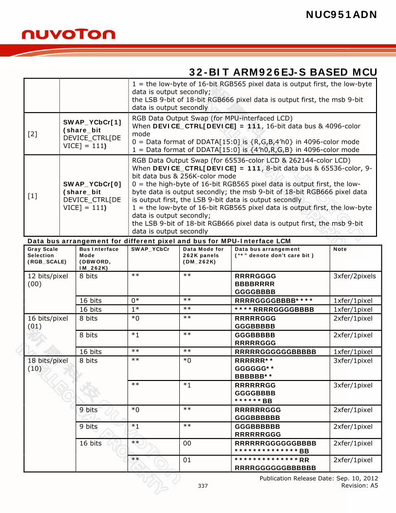
NUC951ADN
32-BIT ARM926EJ-S BASED MCU
Publication Release Date: Sep. 10, 2012 Revision: A5
337
1 = the low-byte of 16-bit RGB565 pixel data is output first, the low-byte data is output secondly; the LSB 9-bit of 18-bit RGB666 pixel data is output first, the msb 9-bit data is output secondly
[2]
SWAP_YCbCr[1] (share_bit DEVICE_CTRL[DEVICE] = 111)
RGB Data Output Swap (for MPU-interfaced LCD) When DEVICE_CTRL[DEVICE] = 111, 16-bit data bus & 4096-color mode 0 = Data format of DDATA[15:0] is R,G,B,4’h0 in 4096-color mode 1 = Data format of DDATA[15:0] is 4’h0,R,G,B in 4096-color mode
[1]
SWAP_YCbCr[0] (share_bit DEVICE_CTRL[DEVICE] = 111)
RGB Data Output Swap (for 65536-color LCD & 262144-color LCD) When DEVICE_CTRL[DEVICE] = 111, 8-bit data bus & 65536-color, 9-bit data bus & 256K-color mode 0 = the high-byte of 16-bit RGB565 pixel data is output first, the low-byte data is output secondly; the msb 9-bit of 18-bit RGB666 pixel data is output first, the LSB 9-bit data is output secondly 1 = the low-byte of 16-bit RGB565 pixel data is output first, the low-byte data is output secondly; the LSB 9-bit of 18-bit RGB666 pixel data is output first, the msb 9-bit data is output secondly
Data bus arrangement for different pixel and bus for MPU-Interface LCM Gray Scale Selection (RGB_SCALE)
Bus Interface Mode (DBWORD, IM_262K)
SWAP_YCbCr Data Mode for 262K panels (DM_262K)
Data bus arrangement (“*” denote don’t care bit )
Note
12 bits/pixel (00)
8 bits ** ** RRRRGGGG BBBBRRRR GGGGBBBB
3xfer/2pixels
16 bits 0* ** RRRRGGGGBBBB**** 1xfer/1pixel 16 bits 1* ** ****RRRRGGGGBBBB 1xfer/1pixel
16 bits/pixel (01)
8 bits *0 ** RRRRRGGG GGGBBBBB
2xfer/1pixel
8 bits *1 ** GGGBBBBB RRRRRGGG
2xfer/1pixel
16 bits ** ** RRRRRGGGGGGBBBBB 1xfer/1pixel 18 bits/pixel (10)
8 bits
** *0 RRRRRR** GGGGGG** BBBBBB**
3xfer/1pixel
** *1 RRRRRRGG GGGGBBBB ******BB
3xfer/1pixel
9 bits *0 ** RRRRRRGGG GGGBBBBBB
2xfer/1pixel
9 bits *1 ** GGGBBBBBB RRRRRRGGG
2xfer/1pixel
16 bits
** 00 RRRRRRGGGGGGBBBB **************BB
2xfer/1pixel
** 01 **************RR RRRRGGGGGGBBBBBB
2xfer/1pixel
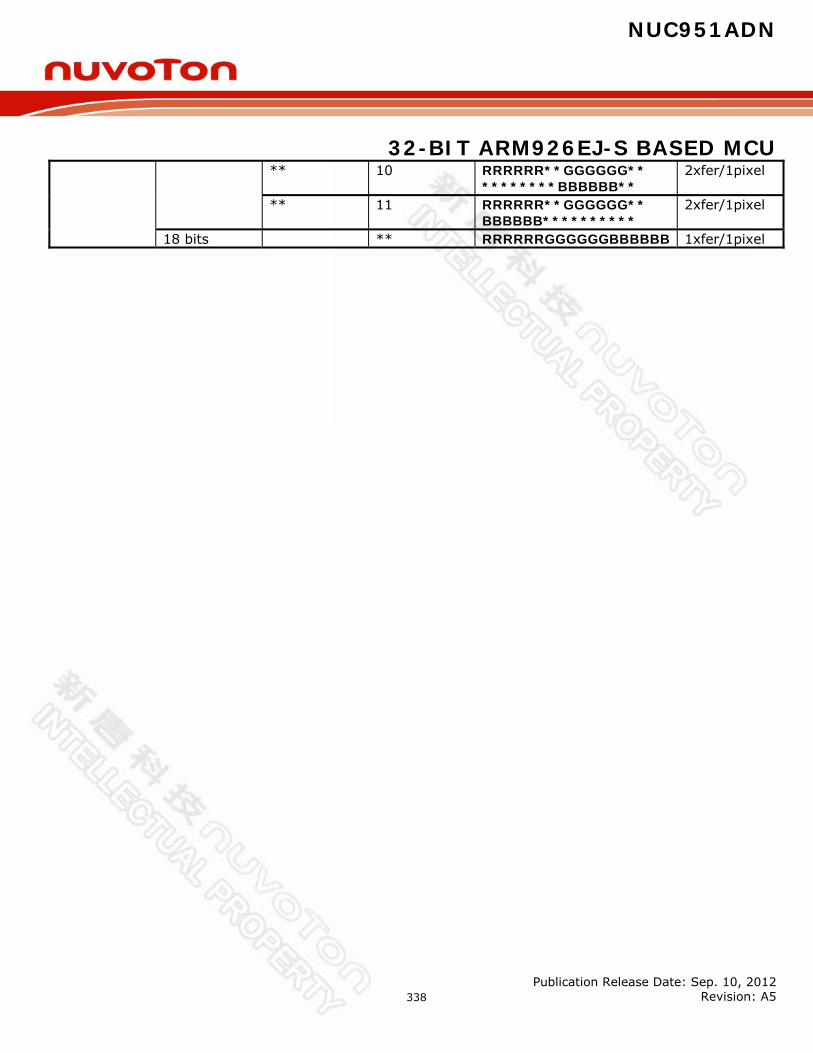
NUC951ADN
32-BIT ARM926EJ-S BASED MCU
Publication Release Date: Sep. 10, 2012 Revision: A5
338
** 10 RRRRRR**GGGGGG** ********BBBBBB**
2xfer/1pixel
** 11 RRRRRR**GGGGGG** BBBBBB**********
2xfer/1pixel
18 bits ** RRRRRRGGGGGGBBBBBB 1xfer/1pixel

NUC951ADN
32-BIT ARM926EJ-S BASED MCU
Publication Release Date: Sep. 10, 2012 Revision: A5
339
Data bus arrangement for different pixel for Unipac - Interface LCM at 16 M colors and 8bits data bus
Gray Scale Selection
Bus Interface Mode (DBWORD)
SWAP_YCbCr Control LCD Line Data Out [LCD_ODD : SEL_ODD]
Data bus arrangement (“*” denote don’t care bit ) First line(odd line)
Data bus arrangement (“*” denote don’t care bit ) second line(even line)
Note
24 bits/pixel
1 00 00 RRRRRRRR0 (pixel 0) GGGGGGGG1 (pixel 1) BBBBBBBB2 (pixel 2)
GGGGGGGG0 (pixel 0) BBBBBBBB1 (pixel 1) RRRRRRRR2 (pixel 2)
1xfer/ 1pixel
1 00 01 BBBBBBBB0 (pixel 0) GGGGGGGG1 (pixel 1) RRRRRRRR2 (pixel 2)
RRRRRRRR0 (pixel 0) BBBBBBBB1 (pixel 1) GGGGGGGG2 (pixel 2)
1xfer/ 1pixel
1 00 10 GGGGGGGG0 (pixel 0) BBBBBBBB1 (pixel 1) RRRRRRRR2 (pixel 2)
RRRRRRRR0 (pixel 0) GGGGGGGG1 (pixel 1) BBBBBBBB2 (pixel 2)
1xfer/ 1pixel
1 00 11 RRRRRRRR0 (pixel 0) BBBBBBBB1 (pixel 1) GGGGGGGG2 (pixel 2)
BBBBBBBB0 (pixel 0) GGGGGGGG1 (pixel 1) RRRRRRRR2 (pixel 2)
1xfer/ 1pixel
1 10 00 RRRRRRRR0 (pixel 0) GGGGGGGG0 (pixel 0) BBBBBBBB1 (pixel 2)
GGGGGGGG0 (pixel 0) BBBBBBBB0 (pixel 0) RRRRRRRR1 (pixel 1)
1.5xfer / 1pixel
1 10 01 BBBBBBBB0 (pixel 0) GGGGGGGG0 (pixel 0) RRRRRRRR1 (pixel 1) BBBBBBBB2 (pixel 2) GGGGGGGG2 (pixel 2) RRRRRRRR3 (pixel 3)
RRRRRRRR0 (pixel 0) BBBBBBBB0 (pixel 0) GGGGGGGG1 (pixel 1) RRRRRRRR2 (pixel 2) BBBBBBBB2 (pixel 2) GGGGGGGG3 (pixel 3)
1.5xfer / 1pixel
1 10 10 GGGGGGGG0 (pixel RRRRRRRR0 (pixel 1.5xfer /
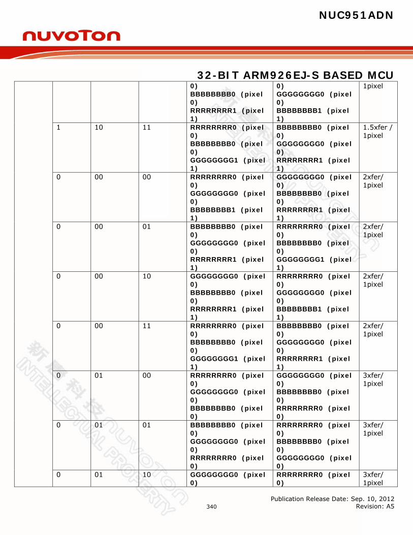
NUC951ADN
32-BIT ARM926EJ-S BASED MCU
Publication Release Date: Sep. 10, 2012 Revision: A5
340
0) BBBBBBBB0 (pixel 0) RRRRRRRR1 (pixel 1)
0) GGGGGGGG0 (pixel 0) BBBBBBBB1 (pixel 1)
1pixel
1 10 11 RRRRRRRR0 (pixel 0) BBBBBBBB0 (pixel 0) GGGGGGGG1 (pixel 1)
BBBBBBBB0 (pixel 0) GGGGGGGG0 (pixel 0) RRRRRRRR1 (pixel 1)
1.5xfer / 1pixel
0 00 00 RRRRRRRR0 (pixel 0) GGGGGGGG0 (pixel 0) BBBBBBBB1 (pixel 1)
GGGGGGGG0 (pixel 0) BBBBBBBB0 (pixel 0) RRRRRRRR1 (pixel 1)
2xfer/ 1pixel
0 00 01 BBBBBBBB0 (pixel 0) GGGGGGGG0 (pixel 0) RRRRRRRR1 (pixel 1)
RRRRRRRR0 (pixel 0) BBBBBBBB0 (pixel 0) GGGGGGGG1 (pixel 1)
2xfer/ 1pixel
0 00 10 GGGGGGGG0 (pixel 0) BBBBBBBB0 (pixel 0) RRRRRRRR1 (pixel 1)
RRRRRRRR0 (pixel 0) GGGGGGGG0 (pixel 0) BBBBBBBB1 (pixel 1)
2xfer/ 1pixel
0 00 11 RRRRRRRR0 (pixel 0) BBBBBBBB0 (pixel 0) GGGGGGGG1 (pixel 1)
BBBBBBBB0 (pixel 0) GGGGGGGG0 (pixel 0) RRRRRRRR1 (pixel 1)
2xfer/ 1pixel
0 01 00 RRRRRRRR0 (pixel 0) GGGGGGGG0 (pixel 0) BBBBBBBB0 (pixel 0)
GGGGGGGG0 (pixel 0) BBBBBBBB0 (pixel 0) RRRRRRRR0 (pixel 0)
3xfer/ 1pixel
0 01 01 BBBBBBBB0 (pixel 0) GGGGGGGG0 (pixel 0) RRRRRRRR0 (pixel 0)
RRRRRRRR0 (pixel 0) BBBBBBBB0 (pixel 0) GGGGGGGG0 (pixel 0)
3xfer/ 1pixel
0 01 10 GGGGGGGG0 (pixel 0)
RRRRRRRR0 (pixel 0)
3xfer/ 1pixel

NUC951ADN
32-BIT ARM926EJ-S BASED MCU
Publication Release Date: Sep. 10, 2012 Revision: A5
341
BBBBBBBB0 (pixel 0) RRRRRRRR0 (pixel 0)
GGGGGGGG0 (pixel 0) BBBBBBBB0 (pixel 0)
0 01 11 RRRRRRRR0 (pixel 0) BBBBBBBB0 (pixel 0) GGGGGGGG0 (pixel 0)
BBBBBBBB0 (pixel 0) GGGGGGGG0 (pixel 0) RRRRRRRR0 (pixel 0)
3xfer/ 1pixel
Data bus arrangement for different pixel for TFT High colors device - Interface LCM at 16 M colors and 8bits data bus
Gray Scale Selection
Bus Interface Mode (DBWORD)
SWAP_YCbCr Control LCD Line Data Out [LCD_ODD : SEL_ODD]
Data bus arrangement (“*” denote don’t care bit )
Note
24 bits data bus
1 00 ** RRRRRRRRGGGGGGGGBBBBBBBB (pixel 0)
1xfer/ 1pixel
8 bits data bus
0 00 ** BBBBBBBB0 (pixel 0) GGGGGGGG0 (pixel 0) RRRRRRRR0 (pixel 0) BBBBBBBB1 (pixel 1) GGGGGGGG1 (pixel 1) RRRRRRRR1 (pixel 1)
3xfer/ 1pixel
0 10 ** BBBBBBBB0 (pixel 0) GGGGGGGG0 (pixel 0) RRRRRRRR0 (pixel 0) ********0 (pixel 0) BBBBBBBB1 (pixel 1) GGGGGGGG1 (pixel 1) RRRRRRRR1 (pixel 1) ********1 (pixel 1)
4xfer/ 1pixel
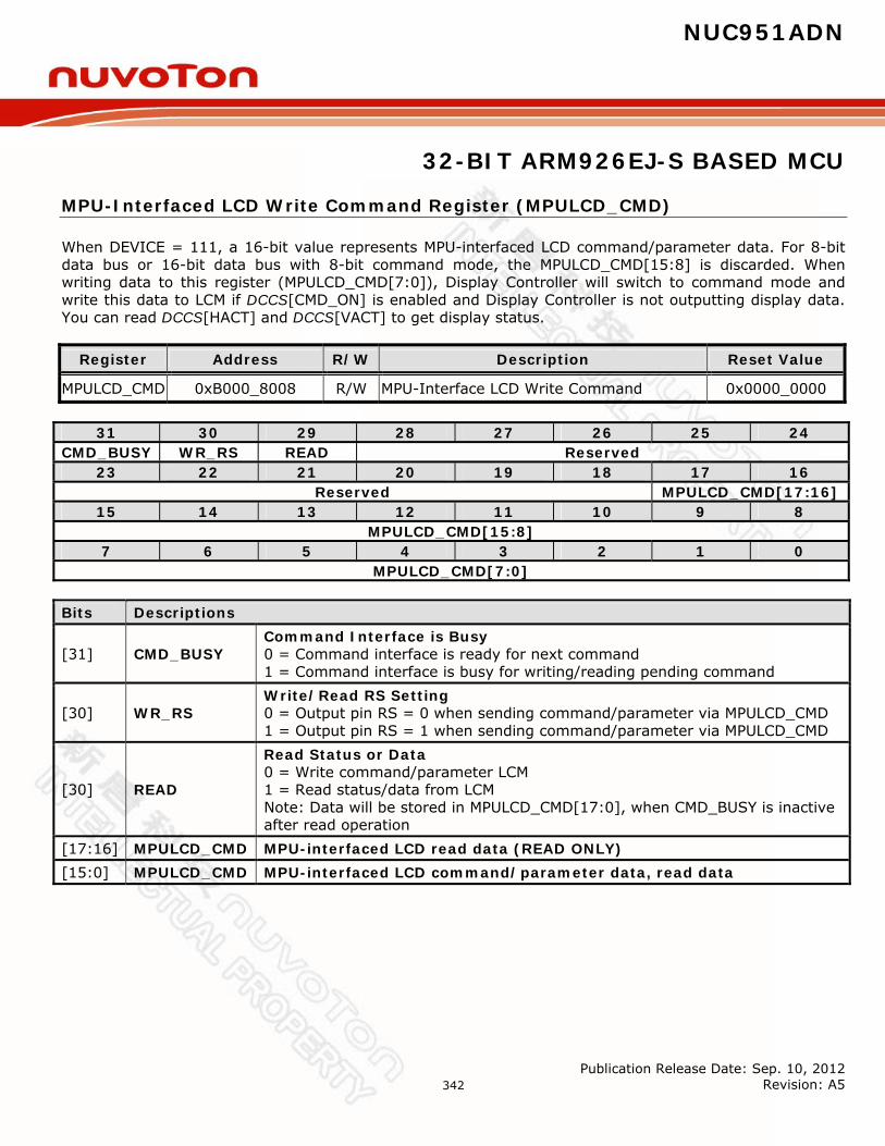
NUC951ADN
32-BIT ARM926EJ-S BASED MCU
Publication Release Date: Sep. 10, 2012 Revision: A5
342
MPU-Interfaced LCD Write Command Register (MPULCD_CMD)
When DEVICE = 111, a 16-bit value represents MPU-interfaced LCD command/parameter data. For 8-bit data bus or 16-bit data bus with 8-bit command mode, the MPULCD_CMD[15:8] is discarded. When writing data to this register (MPULCD_CMD[7:0]), Display Controller will switch to command mode and write this data to LCM if DCCS[CMD_ON] is enabled and Display Controller is not outputting display data. You can read DCCS[HACT] and DCCS[VACT] to get display status.
Register Address R/W Description Reset Value
MPULCD_CMD 0xB000_8008 R/W MPU-Interface LCD Write Command 0x0000_0000
31 30 29 28 27 26 25 24 CMD_BUSY WR_RS READ Reserved
23 22 21 20 19 18 17 16 Reserved MPULCD_CMD[17:16]
15 14 13 12 11 10 9 8 MPULCD_CMD[15:8]
7 6 5 4 3 2 1 0 MPULCD_CMD[7:0]
Bits Descriptions
[31] CMD_BUSY Command Interface is Busy 0 = Command interface is ready for next command 1 = Command interface is busy for writing/reading pending command
[30] WR_RS Write/Read RS Setting 0 = Output pin RS = 0 when sending command/parameter via MPULCD_CMD 1 = Output pin RS = 1 when sending command/parameter via MPULCD_CMD
[30] READ
Read Status or Data 0 = Write command/parameter LCM 1 = Read status/data from LCM Note: Data will be stored in MPULCD_CMD[17:0], when CMD_BUSY is inactive after read operation
[17:16] MPULCD_CMD MPU-interfaced LCD read data (READ ONLY) [15:0] MPULCD_CMD MPU-interfaced LCD command/parameter data, read data
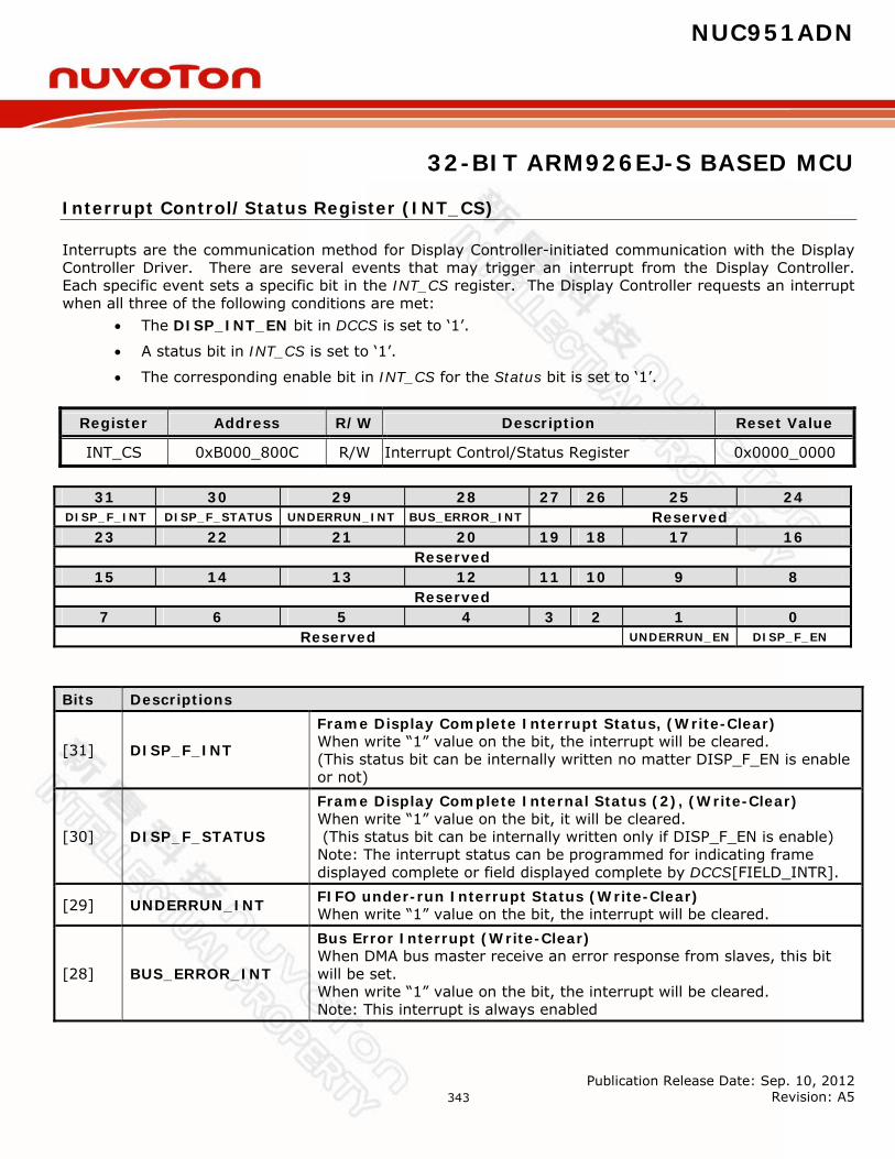
NUC951ADN
32-BIT ARM926EJ-S BASED MCU
Publication Release Date: Sep. 10, 2012 Revision: A5
343
Interrupt Control/Status Register (INT_CS)
Interrupts are the communication method for Display Controller-initiated communication with the Display Controller Driver. There are several events that may trigger an interrupt from the Display Controller. Each specific event sets a specific bit in the INT_CS register. The Display Controller requests an interrupt when all three of the following conditions are met:
The DISP_INT_EN bit in DCCS is set to ‘1’.
A status bit in INT_CS is set to ‘1’.
The corresponding enable bit in INT_CS for the Status bit is set to ‘1’.
Register Address R/W Description Reset Value
INT_CS 0xB000_800C R/W Interrupt Control/Status Register 0x0000_0000
31 30 29 28 27 26 25 24 DISP_F_INT DISP_F_STATUS UNDERRUN_INT BUS_ERROR_INT Reserved
23 22 21 20 19 18 17 16 Reserved
15 14 13 12 11 10 9 8 Reserved
7 6 5 4 3 2 1 0 Reserved UNDERRUN_EN DISP_F_EN
Bits Descriptions
[31] DISP_F_INT
Frame Display Complete Interrupt Status, (Write-Clear) When write “1” value on the bit, the interrupt will be cleared. (This status bit can be internally written no matter DISP_F_EN is enable or not)
[30] DISP_F_STATUS
Frame Display Complete Internal Status (2), (Write-Clear) When write “1” value on the bit, it will be cleared. (This status bit can be internally written only if DISP_F_EN is enable) Note: The interrupt status can be programmed for indicating frame displayed complete or field displayed complete by DCCS[FIELD_INTR].
[29] UNDERRUN_INT FIFO under-run Interrupt Status (Write-Clear) When write “1” value on the bit, the interrupt will be cleared.
[28] BUS_ERROR_INT
Bus Error Interrupt (Write-Clear) When DMA bus master receive an error response from slaves, this bit will be set. When write “1” value on the bit, the interrupt will be cleared. Note: This interrupt is always enabled
NUC951ADN
32-BIT ARM926EJ-S BASED MCU
Publication Release Date: Sep. 10, 2012 Revision: A5
344
[1] UNDERRUN_EN FIFO under-run Interrupt Enable 0 = Disable 1 = Enable
[0] DISP_F_EN Frame Display Complete Interrupt Enable 0 = Disable 1 = Enable

NUC951ADN
32-BIT ARM926EJ-S BASED MCU
Publication Release Date: Sep. 10, 2012 Revision: A5
345
CRTC Display Size Register (CRTC_SIZE)
This register controls the display size. It includes Horizontal-Total (HTT) and Vertical-Total (VTT) registers. The value of HTT specifies the total number of pixels in the CRTC horizontal scan line interval including retrace time. And the value of VTT specifies the total number of scan line for each field (frame), including the retrace time.
Register Address R/W Description Reset Value
CRTC_SIZE 0xB000_8010 R/W CRTC Display Size 0x0000_0000
31 30 29 28 27 26 25 24 Reserved VTT[10:8]
23 22 21 20 19 18 17 16 VTT[7:0]
15 14 13 12 11 10 9 8 Reserved HTT[10:8]
7 6 5 4 3 2 1 0 HTT[7:0]
Bits Descriptions
[26:16] VTT[10:0] CRTC Vertical Total Scan Lines An 11-bits value specifies the total number of scan line for each field, including the retrace time
[10:0] HTT[10:0] CRTC Horizontal Total Pixels An 11-bits value specifies the total number of pixels in the CRTC horizontal scan line interval including the retrace time

NUC951ADN
32-BIT ARM926EJ-S BASED MCU
Publication Release Date: Sep. 10, 2012 Revision: A5
346
CRTC Display Enable End Register (CRTC_DEND)
This register controls the actual display size of the output device. It includes HDEND and VDEND registers. The value of HDEND specifies the total number of displayed pixels for a scan line. And the value of VDEND specifies the total number of displayed scan line for each field (frame).
Register Address R/W Description Reset Value
CRTC_DEND 0xB000_8014 R/W CRTC Display Enable End 0x0000_0000
31 30 29 28 27 26 25 24 Reserved VDEND[10:8]
23 22 21 20 19 18 17 16 VDEND[7:0]
15 14 13 12 11 10 9 8 Reserved HDEND[10:8]
7 6 5 4 3 2 1 0 HDEND[7:0]
Bits Descriptions
[26:16] VDEND[10:0] CRTC Vertical Display Enable End An 11-bits value specifies the total number of displayed scan line for each field.
[10:0] HDND[10:0] CRTC Horizontal Display Enable End An 11-bits value specifies the total number of displayed pixels for scan line.
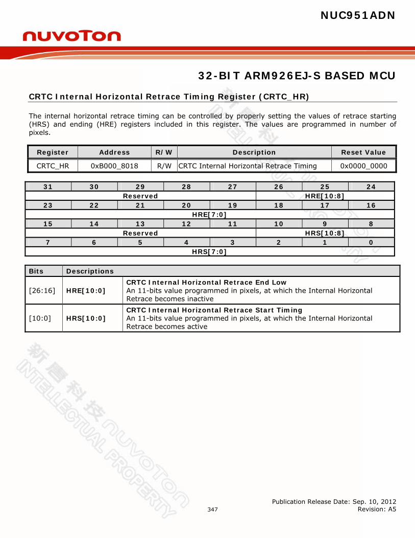
NUC951ADN
32-BIT ARM926EJ-S BASED MCU
Publication Release Date: Sep. 10, 2012 Revision: A5
347
CRTC Internal Horizontal Retrace Timing Register (CRTC_HR)
The internal horizontal retrace timing can be controlled by properly setting the values of retrace starting (HRS) and ending (HRE) registers included in this register. The values are programmed in number of pixels.
Register Address R/W Description Reset Value
CRTC_HR 0xB000_8018 R/W CRTC Internal Horizontal Retrace Timing 0x0000_0000
31 30 29 28 27 26 25 24 Reserved HRE[10:8]
23 22 21 20 19 18 17 16 HRE[7:0]
15 14 13 12 11 10 9 8 Reserved HRS[10:8]
7 6 5 4 3 2 1 0 HRS[7:0]
Bits Descriptions
[26:16] HRE[10:0] CRTC Internal Horizontal Retrace End Low An 11-bits value programmed in pixels, at which the Internal Horizontal Retrace becomes inactive
[10:0] HRS[10:0] CRTC Internal Horizontal Retrace Start Timing An 11-bits value programmed in pixels, at which the Internal Horizontal Retrace becomes active

NUC951ADN
32-BIT ARM926EJ-S BASED MCU
Publication Release Date: Sep. 10, 2012 Revision: A5
348
CRTC Horizontal Sync Timing Register (CRTC_HSYNC)
The horizontal sync timing can be controlled by properly setting the values of starting (HSYNC_S) and ending (HSYNC_E) registers included in this register. The values are programmed in numbers of pixel.
Register Address R/W Description Reset Value
CRTC_HSYNC 0xB000_801C R/W CRTC Horizontal Sync Timing 0x0000_0000
31 30 29 28 27 26 25 24 HSYNC_SHIFT [1:0] Reserved HSYNC_E[10:8]
23 22 21 20 19 18 17 16 HSYNC_E[7:0]
15 14 13 12 11 10 9 8 Reserved HSYNC_S[10:8]
7 6 5 4 3 2 1 0 HSYNC_S[7:0]
Bits Descriptions
[10:0] HSYNC_S[10:0] CRTC Horizontal Sync Start Timing An 11-bits value programmed in pixels, at which the Horizontal Sync signal becomes active
[26:16] HSYNC_E[10:0] CRTC Horizontal Sync End Timing An 11-bits value programmed in pixels, at which the Horizontal Sync Signal becomes inactive
[31:30] HSYNC_SHIFT [1:0]
Hsync signal adjustment for multi-cycles per pixel mode of Sync-based Unipac-LCD
When DEVICE_CTRL[DEVICE] = 100,8-bit data bus, DEVICE[DBWORD]= 0, and DEVICE_CTRL[SWAP_YcbCr[1]]=0,
If DEVICE_CTRL[SWAP_YcbCr[0]]= 0, it means that 2 cycles per pixel, so hsync’s hrs would move three cycles if hrs added or subtracted 1.In order to adjust hsync signal in pclk unit, RGB_SHIFT shared register aids this function in -LCD with 8 bits data bus mode.
HSYNC_SHIFT = 0 : hsync will not move
HSYNC _SHIFT = 1 : hsync will left move 1 pclk cycle
If DEVICE_CTRL[SWAP_YcbCr[0]] = 1, it means that 3 cycles per pixel, so hsync’s hrs would move three cycles if hrs added or subtracted 1.In order to adjust hsync signal in pclk unit, RGB_SHIFT shared register aids this
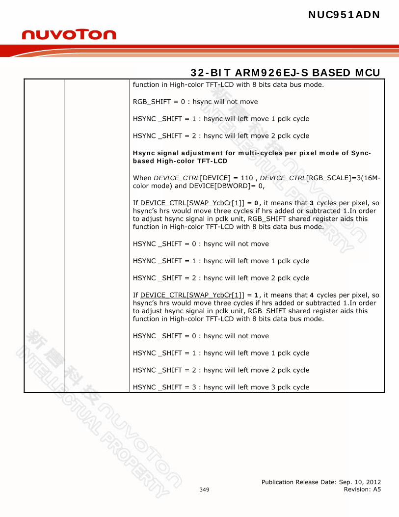
NUC951ADN
32-BIT ARM926EJ-S BASED MCU
Publication Release Date: Sep. 10, 2012 Revision: A5
349
function in High-color TFT-LCD with 8 bits data bus mode.
RGB_SHIFT = 0 : hsync will not move
HSYNC _SHIFT = 1 : hsync will left move 1 pclk cycle
HSYNC _SHIFT = 2 : hsync will left move 2 pclk cycle
Hsync signal adjustment for multi-cycles per pixel mode of Sync-based High-color TFT-LCD
When DEVICE_CTRL[DEVICE] = 110 , DEVICE_CTRL[RGB_SCALE]=3(16M-color mode) and DEVICE[DBWORD]= 0,
If DEVICE_CTRL[SWAP_YcbCr[1]] = 0, it means that 3 cycles per pixel, so hsync’s hrs would move three cycles if hrs added or subtracted 1.In order to adjust hsync signal in pclk unit, RGB_SHIFT shared register aids this function in High-color TFT-LCD with 8 bits data bus mode.
HSYNC _SHIFT = 0 : hsync will not move
HSYNC _SHIFT = 1 : hsync will left move 1 pclk cycle
HSYNC _SHIFT = 2 : hsync will left move 2 pclk cycle
If DEVICE_CTRL[SWAP_YcbCr[1]] = 1, it means that 4 cycles per pixel, so hsync’s hrs would move three cycles if hrs added or subtracted 1.In order to adjust hsync signal in pclk unit, RGB_SHIFT shared register aids this function in High-color TFT-LCD with 8 bits data bus mode.
HSYNC _SHIFT = 0 : hsync will not move
HSYNC _SHIFT = 1 : hsync will left move 1 pclk cycle
HSYNC _SHIFT = 2 : hsync will left move 2 pclk cycle
HSYNC _SHIFT = 3 : hsync will left move 3 pclk cycle

NUC951ADN
32-BIT ARM926EJ-S BASED MCU
Publication Release Date: Sep. 10, 2012 Revision: A5
350
CRTC Internal Vertical Retrace Timing Register (CRTC_VR)
The vertical retrace timing can be controlled by properly setting the values of starting (VRS) and ending (VRE) registers included in this register. The values are programmed in numbers of scan-line.
Register Address R/W Description Reset Value
CRTC_VR 0xB000_8020 R/W CRTC Internal Vertical Retrace Timing 0x0000_0000
31 30 29 28 27 26 25 24 Reserved VRE[10:8]
23 22 21 20 19 18 17 16 VRE[7:0]
15 14 13 12 11 10 9 8 Reserved VRS[10:8]
7 6 5 4 3 2 1 0 VRS[7:0]
Bits Descriptions
[26:16] VRE[10:0] CRTC Vertical Internal Retrace End Low An 11-bits value is programmed in number of scan line, at which the internal vertical retrace becomes inactive.
[10:0] VRS[10:0] CRTC Vertical Internal Retrace Start Timing An 11-bits value is programmed in number of scan line, at which the internal vertical retrace becomes active
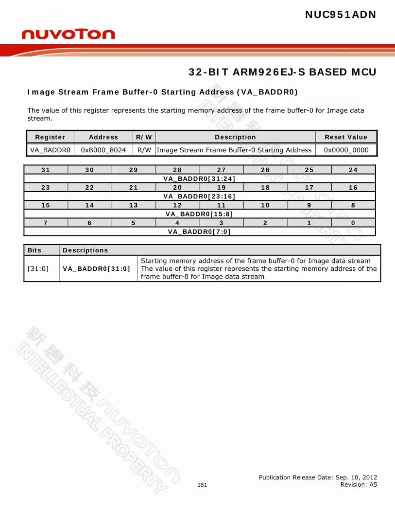
NUC951ADN
32-BIT ARM926EJ-S BASED MCU
Publication Release Date: Sep. 10, 2012 Revision: A5
351
Image Stream Frame Buffer-0 Starting Address (VA_BADDR0)
The value of this register represents the starting memory address of the frame buffer-0 for Image data stream.
Register Address R/W Description Reset Value
VA_BADDR0 0xB000_8024 R/W Image Stream Frame Buffer-0 Starting Address 0x0000_0000
31 30 29 28 27 26 25 24 VA_BADDR0[31:24]
23 22 21 20 19 18 17 16 VA_BADDR0[23:16]
15 14 13 12 11 10 9 8 VA_BADDR0[15:8]
7 6 5 4 3 2 1 0 VA_BADDR0[7:0]
Bits Descriptions
[31:0] VA_BADDR0[31:0] Starting memory address of the frame buffer-0 for Image data stream The value of this register represents the starting memory address of the frame buffer-0 for Image data stream.
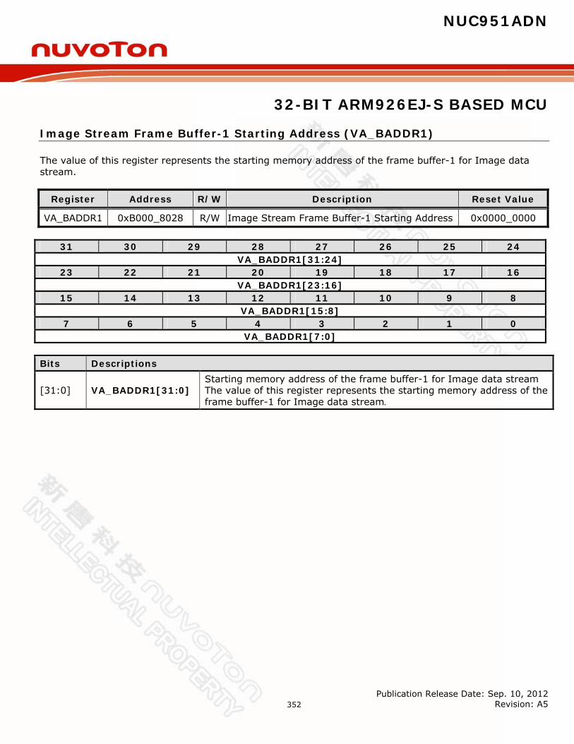
NUC951ADN
32-BIT ARM926EJ-S BASED MCU
Publication Release Date: Sep. 10, 2012 Revision: A5
352
Image Stream Frame Buffer-1 Starting Address (VA_BADDR1)
The value of this register represents the starting memory address of the frame buffer-1 for Image data stream.
Register Address R/W Description Reset Value
VA_BADDR1 0xB000_8028 R/W Image Stream Frame Buffer-1 Starting Address 0x0000_0000
31 30 29 28 27 26 25 24 VA_BADDR1[31:24]
23 22 21 20 19 18 17 16 VA_BADDR1[23:16]
15 14 13 12 11 10 9 8 VA_BADDR1[15:8]
7 6 5 4 3 2 1 0 VA_BADDR1[7:0]
Bits Descriptions
[31:0] VA_BADDR1[31:0] Starting memory address of the frame buffer-1 for Image data stream The value of this register represents the starting memory address of the frame buffer-1 for Image data stream.
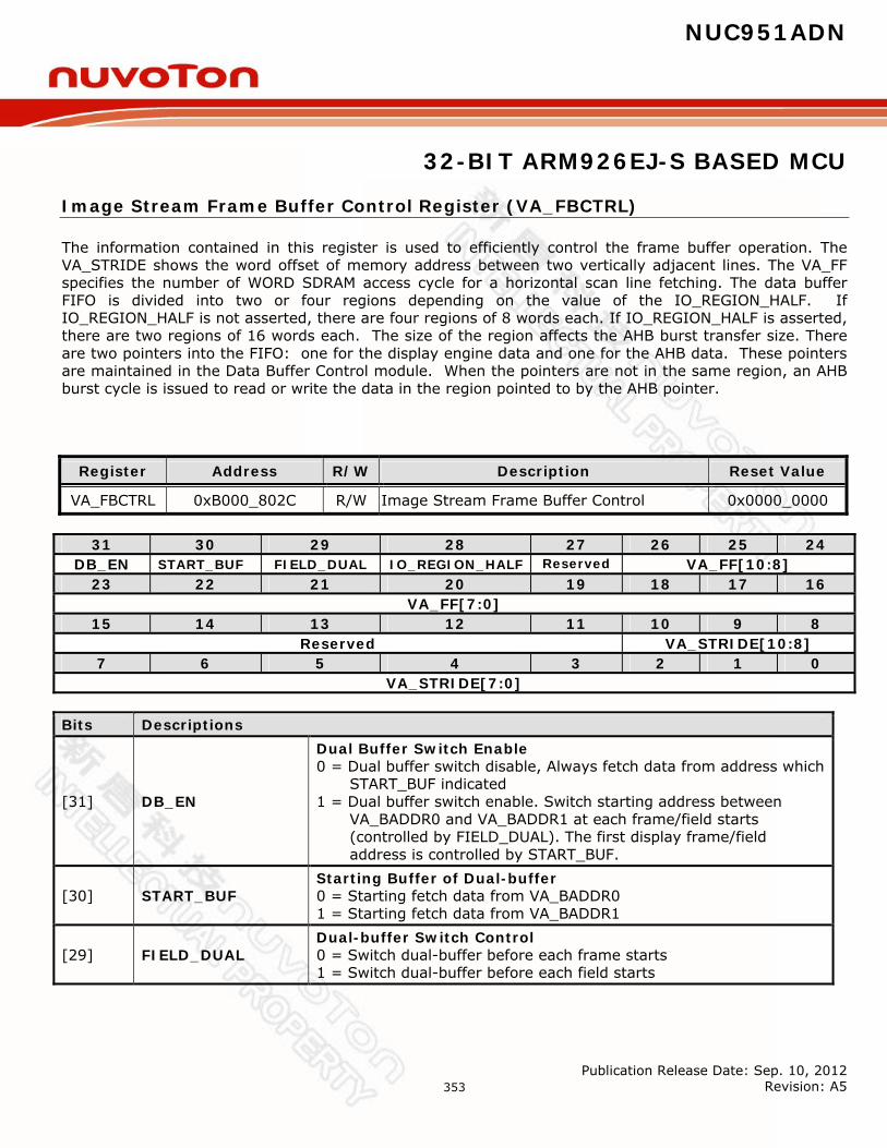
NUC951ADN
32-BIT ARM926EJ-S BASED MCU
Publication Release Date: Sep. 10, 2012 Revision: A5
353
Image Stream Frame Buffer Control Register (VA_FBCTRL)
The information contained in this register is used to efficiently control the frame buffer operation. The VA_STRIDE shows the word offset of memory address between two vertically adjacent lines. The VA_FF specifies the number of WORD SDRAM access cycle for a horizontal scan line fetching. The data buffer FIFO is divided into two or four regions depending on the value of the IO_REGION_HALF. If IO_REGION_HALF is not asserted, there are four regions of 8 words each. If IO_REGION_HALF is asserted, there are two regions of 16 words each. The size of the region affects the AHB burst transfer size. There are two pointers into the FIFO: one for the display engine data and one for the AHB data. These pointers are maintained in the Data Buffer Control module. When the pointers are not in the same region, an AHB burst cycle is issued to read or write the data in the region pointed to by the AHB pointer.
Register Address R/W Description Reset Value
VA_FBCTRL 0xB000_802C R/W Image Stream Frame Buffer Control 0x0000_0000
31 30 29 28 27 26 25 24 DB_EN START_BUF FIELD_DUAL IO_REGION_HALF Reserved VA_FF[10:8]
23 22 21 20 19 18 17 16 VA_FF[7:0]
15 14 13 12 11 10 9 8 Reserved VA_STRIDE[10:8]
7 6 5 4 3 2 1 0 VA_STRIDE[7:0]
Bits Descriptions
[31] DB_EN
Dual Buffer Switch Enable 0 = Dual buffer switch disable, Always fetch data from address which
START_BUF indicated 1 = Dual buffer switch enable. Switch starting address between
VA_BADDR0 and VA_BADDR1 at each frame/field starts (controlled by FIELD_DUAL). The first display frame/field address is controlled by START_BUF.
[30] START_BUF Starting Buffer of Dual-buffer 0 = Starting fetch data from VA_BADDR0 1 = Starting fetch data from VA_BADDR1
[29] FIELD_DUAL Dual-buffer Switch Control 0 = Switch dual-buffer before each frame starts 1 = Switch dual-buffer before each field starts
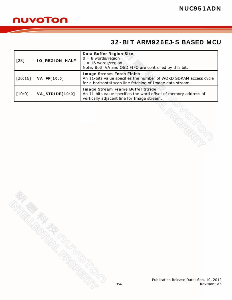
NUC951ADN
32-BIT ARM926EJ-S BASED MCU
Publication Release Date: Sep. 10, 2012 Revision: A5
354
[28] IO_REGION_HALF
Data Buffer Region Size 0 = 8 words/region 1 = 16 words/region Note: Both VA and OSD FIFO are controlled by this bit.
[26:16] VA_FF[10:0] Image Stream Fetch Finish An 11-bits value specifies the number of WORD SDRAM access cycle for a horizontal scan line fetching of Image data stream.
[10:0] VA_STRIDE[10:0] Image Stream Frame Buffer Stride An 11-bits value specifies the word offset of memory address of vertically adjacent line for Image stream.
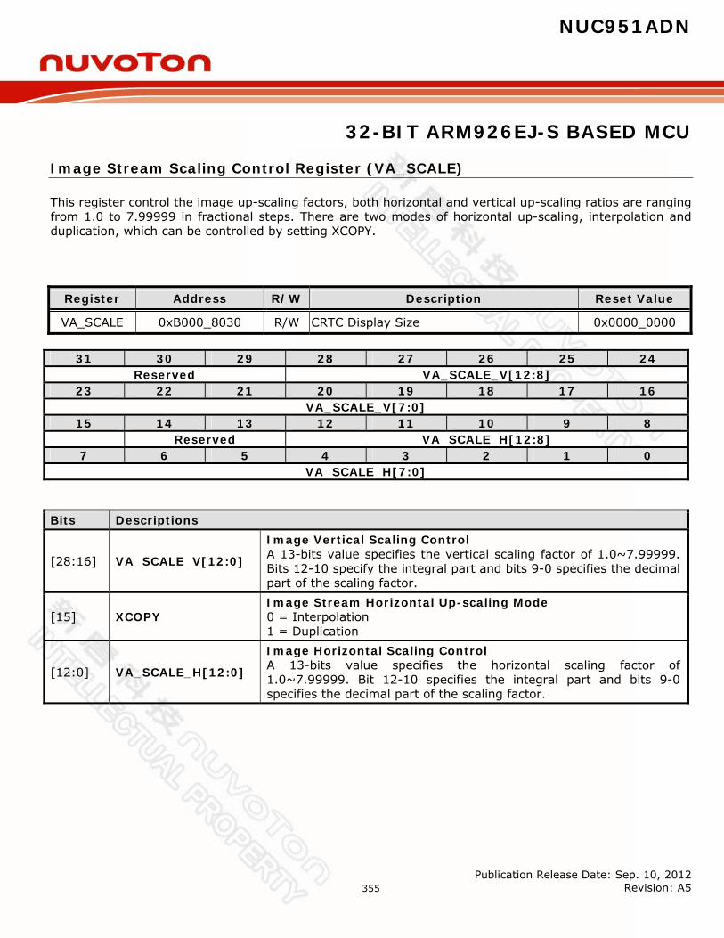
NUC951ADN
32-BIT ARM926EJ-S BASED MCU
Publication Release Date: Sep. 10, 2012 Revision: A5
355
Image Stream Scaling Control Register (VA_SCALE)
This register control the image up-scaling factors, both horizontal and vertical up-scaling ratios are ranging from 1.0 to 7.99999 in fractional steps. There are two modes of horizontal up-scaling, interpolation and duplication, which can be controlled by setting XCOPY.
Register Address R/W Description Reset Value
VA_SCALE 0xB000_8030 R/W CRTC Display Size 0x0000_0000
31 30 29 28 27 26 25 24 Reserved VA_SCALE_V[12:8]
23 22 21 20 19 18 17 16 VA_SCALE_V[7:0]
15 14 13 12 11 10 9 8 Reserved VA_SCALE_H[12:8]
7 6 5 4 3 2 1 0 VA_SCALE_H[7:0]
Bits Descriptions
[28:16] VA_SCALE_V[12:0]
Image Vertical Scaling Control A 13-bits value specifies the vertical scaling factor of 1.0~7.99999. Bits 12-10 specify the integral part and bits 9-0 specifies the decimal part of the scaling factor.
[15] XCOPY Image Stream Horizontal Up-scaling Mode 0 = Interpolation 1 = Duplication
[12:0] VA_SCALE_H[12:0]
Image Horizontal Scaling Control A 13-bits value specifies the horizontal scaling factor of 1.0~7.99999. Bit 12-10 specifies the integral part and bits 9-0 specifies the decimal part of the scaling factor.
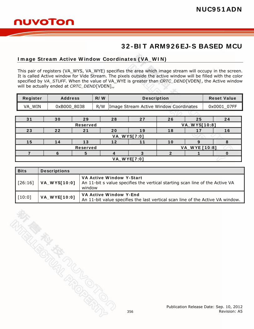
NUC951ADN
32-BIT ARM926EJ-S BASED MCU
Publication Release Date: Sep. 10, 2012 Revision: A5
356
Image Stream Active Window Coordinates (VA_WIN)
This pair of registers (VA_WYS, VA_WYE) specifies the area which image stream will occupy in the screen. It is called Active window for Vide Stream. The pixels outside the active window will be filled with the color specified by VA_STUFF. When the value of VA_WYE is greater than CRTC_DEND[VDEN], the Active window will be actually ended at CRTC_DEND[VDEN],,
Register Address R/W Description Reset Value
VA_WIN 0xB000_8038 R/W Image Stream Active Window Coordinates 0x0001_07FF
31 30 29 28 27 26 25 24 Reserved VA_WYS[10:8]
23 22 21 20 19 18 17 16 VA_WYS[7:0]
15 14 13 12 11 10 9 8 Reserved VA_WYE [10:8]
7 6 5 4 3 2 1 0 VA_WYE[7:0]
Bits Descriptions
[26:16] VA_WYS[10:0] VA Active Window Y-Start An 11-bit s value specifies the vertical starting scan line of the Active VA window
[10:0] VA_WYE[10:0] VA Active Window Y-End An 11-bit value specifies the last vertical scan line of the Active VA window.
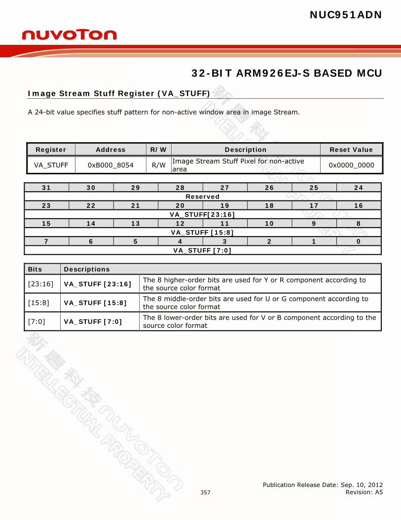
NUC951ADN
32-BIT ARM926EJ-S BASED MCU
Publication Release Date: Sep. 10, 2012 Revision: A5
357
Image Stream Stuff Register (VA_STUFF)
A 24-bit value specifies stuff pattern for non-active window area in image Stream.
Register Address R/W Description Reset Value
VA_STUFF 0xB000_8054 R/W Image Stream Stuff Pixel for non-active area 0x0000_0000
31 30 29 28 27 26 25 24
Reserved 23 22 21 20 19 18 17 16
VA_STUFF[23:16] 15 14 13 12 11 10 9 8
VA_STUFF [15:8] 7 6 5 4 3 2 1 0
VA_STUFF [7:0] Bits Descriptions
[23:16] VA_STUFF [23:16] The 8 higher-order bits are used for Y or R component according to the source color format
[15:8] VA_STUFF [15:8] The 8 middle-order bits are used for U or G component according to the source color format
[7:0] VA_STUFF [7:0] The 8 lower-order bits are used for V or B component according to the source color format

NUC951ADN
32-BIT ARM926EJ-S BASED MCU
Publication Release Date: Sep. 10, 2012 Revision: A5
358
OSD Window Starting Coordinates Register (OSD_WINS)
The starting coordinates of the OSD window is specified in this register. Two values form the coordinates; they are the horizontal starting pixel (OSD_WXS) and the vertical starting scan line (OSD_WYS).
Register Address R/W Description Reset Value
OSD_WINS 0xB000_8040 R/W OSD Window Starting Coordinates Timing 0x0000_0000
31 30 29 28 27 26 25 24 Reserved OSD_WYS[10:8]
23 22 21 20 19 18 17 16 OSD_WYS[7:0]
15 14 13 12 11 10 9 8 Reserved OSD_WXS [10:8]
7 6 5 4 3 2 1 0 OSD_WXS[7:0]
Bits Descriptions
[26:16] OSD_WYS[10:0] OSD Window Y-Start An 11-bit s value specifies the vertical starting scan line of the OSD window
[10:0] OSD_WXS[10:0] OSD Window X-Start An 11-bits value specifies the horizontal starting pixel position of the OSD window.
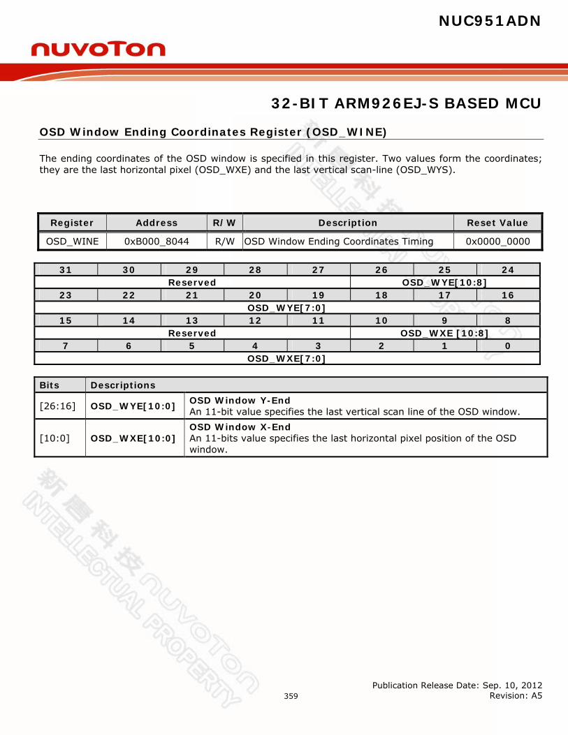
NUC951ADN
32-BIT ARM926EJ-S BASED MCU
Publication Release Date: Sep. 10, 2012 Revision: A5
359
OSD Window Ending Coordinates Register (OSD_WINE)
The ending coordinates of the OSD window is specified in this register. Two values form the coordinates; they are the last horizontal pixel (OSD_WXE) and the last vertical scan-line (OSD_WYS).
Register Address R/W Description Reset Value
OSD_WINE 0xB000_8044 R/W OSD Window Ending Coordinates Timing 0x0000_0000
31 30 29 28 27 26 25 24 Reserved OSD_WYE[10:8]
23 22 21 20 19 18 17 16 OSD_WYE[7:0]
15 14 13 12 11 10 9 8 Reserved OSD_WXE [10:8]
7 6 5 4 3 2 1 0 OSD_WXE[7:0]
Bits Descriptions
[26:16] OSD_WYE[10:0] OSD Window Y-End An 11-bit value specifies the last vertical scan line of the OSD window.
[10:0] OSD_WXE[10:0] OSD Window X-End An 11-bits value specifies the last horizontal pixel position of the OSD window.
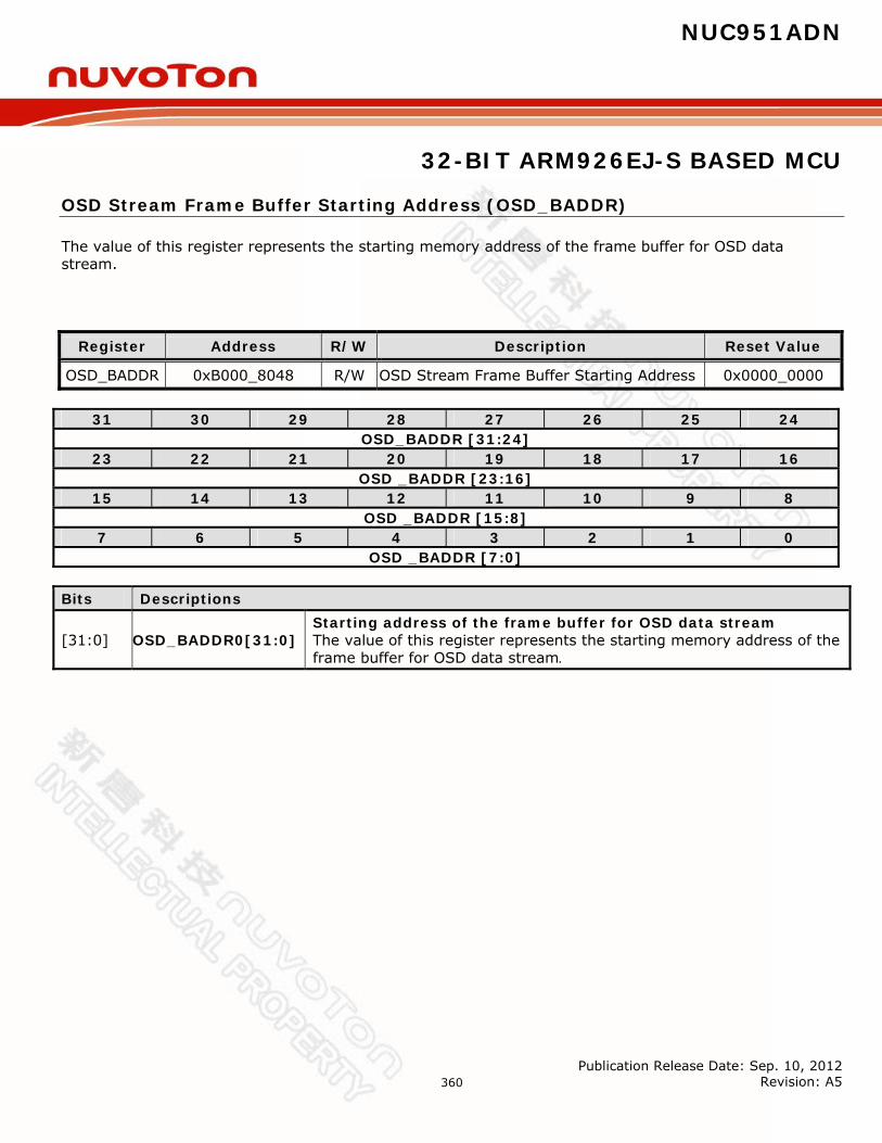
NUC951ADN
32-BIT ARM926EJ-S BASED MCU
Publication Release Date: Sep. 10, 2012 Revision: A5
360
OSD Stream Frame Buffer Starting Address (OSD_BADDR)
The value of this register represents the starting memory address of the frame buffer for OSD data stream.
Register Address R/W Description Reset Value
OSD_BADDR 0xB000_8048 R/W OSD Stream Frame Buffer Starting Address 0x0000_0000
31 30 29 28 27 26 25 24 OSD_BADDR [31:24]
23 22 21 20 19 18 17 16 OSD _BADDR [23:16]
15 14 13 12 11 10 9 8 OSD _BADDR [15:8]
7 6 5 4 3 2 1 0 OSD _BADDR [7:0]
Bits Descriptions
[31:0] OSD_BADDR0[31:0] Starting address of the frame buffer for OSD data stream The value of this register represents the starting memory address of the frame buffer for OSD data stream.
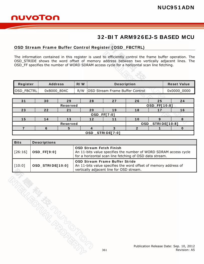
NUC951ADN
32-BIT ARM926EJ-S BASED MCU
Publication Release Date: Sep. 10, 2012 Revision: A5
361
OSD Stream Frame Buffer Control Register (OSD_FBCTRL)
The information contained in this register is used to efficiently control the frame buffer operation. The OSD_STRIDE shows the word offset of memory address between two vertically adjacent lines. The OSD_FF specifies the number of WORD SDRAM access cycle for a horizontal scan line fetching.
Register Address R/W Description Reset Value
OSD_FBCTRL 0xB000_804C R/W OSD Stream Frame Buffer Control 0x0000_0000
31 30 29 28 27 26 25 24 Reserved OSD_FF[10:8]
23 22 21 20 19 18 17 16 OSD_FF[7:0]
15 14 13 12 11 10 9 8 Reserved OSD _STRIDE[10:8]
7 6 5 4 3 2 1 0 OSD _STRIDE[7:0]
Bits Descriptions
[26:16] OSD_FF[9:0] OSD Stream Fetch Finish An 11-bits value specifies the number of WORD SDRAM access cycle for a horizontal scan line fetching of OSD data stream.
[10:0] OSD_STRIDE[10:0] OSD Stream Frame Buffer Stride An 11-bits value specifies the word offset of memory address of vertically adjacent line for OSD stream.
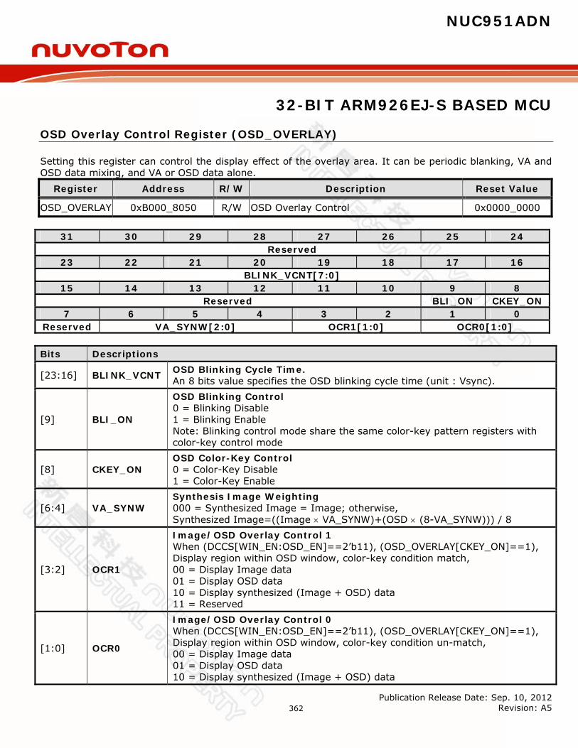
NUC951ADN
32-BIT ARM926EJ-S BASED MCU
Publication Release Date: Sep. 10, 2012 Revision: A5
362
OSD Overlay Control Register (OSD_OVERLAY)
Setting this register can control the display effect of the overlay area. It can be periodic blanking, VA and OSD data mixing, and VA or OSD data alone.
Register Address R/W Description Reset Value
OSD_OVERLAY 0xB000_8050 R/W OSD Overlay Control 0x0000_0000
31 30 29 28 27 26 25 24 Reserved
23 22 21 20 19 18 17 16 BLINK_VCNT[7:0]
15 14 13 12 11 10 9 8 Reserved BLI_ON CKEY_ON
7 6 5 4 3 2 1 0 Reserved VA_SYNW[2:0] OCR1[1:0] OCR0[1:0] Bits Descriptions
[23:16] BLINK_VCNT OSD Blinking Cycle Time. An 8 bits value specifies the OSD blinking cycle time (unit : Vsync).
[9] BLI_ON
OSD Blinking Control 0 = Blinking Disable 1 = Blinking Enable Note: Blinking control mode share the same color-key pattern registers with color-key control mode
[8] CKEY_ON OSD Color-Key Control 0 = Color-Key Disable 1 = Color-Key Enable
[6:4] VA_SYNW Synthesis Image Weighting 000 = Synthesized Image = Image; otherwise, Synthesized Image=((Image VA_SYNW)+(OSD (8-VA_SYNW))) / 8
[3:2] OCR1
Image/OSD Overlay Control 1 When (DCCS[WIN_EN:OSD_EN]==2’b11), (OSD_OVERLAY[CKEY_ON]==1), Display region within OSD window, color-key condition match, 00 = Display Image data 01 = Display OSD data 10 = Display synthesized (Image + OSD) data 11 = Reserved
[1:0] OCR0
Image/OSD Overlay Control 0 When (DCCS[WIN_EN:OSD_EN]==2’b11), (OSD_OVERLAY[CKEY_ON]==1), Display region within OSD window, color-key condition un-match, 00 = Display Image data 01 = Display OSD data 10 = Display synthesized (Image + OSD) data
NUC951ADN
32-BIT ARM926EJ-S BASED MCU
Publication Release Date: Sep. 10, 2012 Revision: A5
363
11 = Reserved
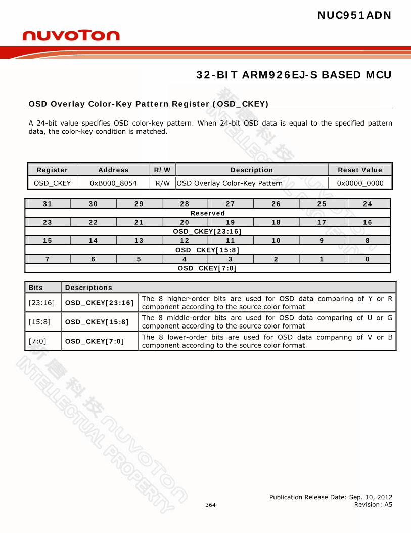
NUC951ADN
32-BIT ARM926EJ-S BASED MCU
Publication Release Date: Sep. 10, 2012 Revision: A5
364
OSD Overlay Color-Key Pattern Register (OSD_CKEY)
A 24-bit value specifies OSD color-key pattern. When 24-bit OSD data is equal to the specified pattern data, the color-key condition is matched.
Register Address R/W Description Reset Value
OSD_CKEY 0xB000_8054 R/W OSD Overlay Color-Key Pattern 0x0000_0000
31 30 29 28 27 26 25 24 Reserved
23 22 21 20 19 18 17 16 OSD_CKEY[23:16]
15 14 13 12 11 10 9 8 OSD_CKEY[15:8]
7 6 5 4 3 2 1 0 OSD_CKEY[7:0]
Bits Descriptions
[23:16] OSD_CKEY[23:16] The 8 higher-order bits are used for OSD data comparing of Y or R component according to the source color format
[15:8] OSD_CKEY[15:8] The 8 middle-order bits are used for OSD data comparing of U or G component according to the source color format
[7:0] OSD_CKEY[7:0] The 8 lower-order bits are used for OSD data comparing of V or B component according to the source color format
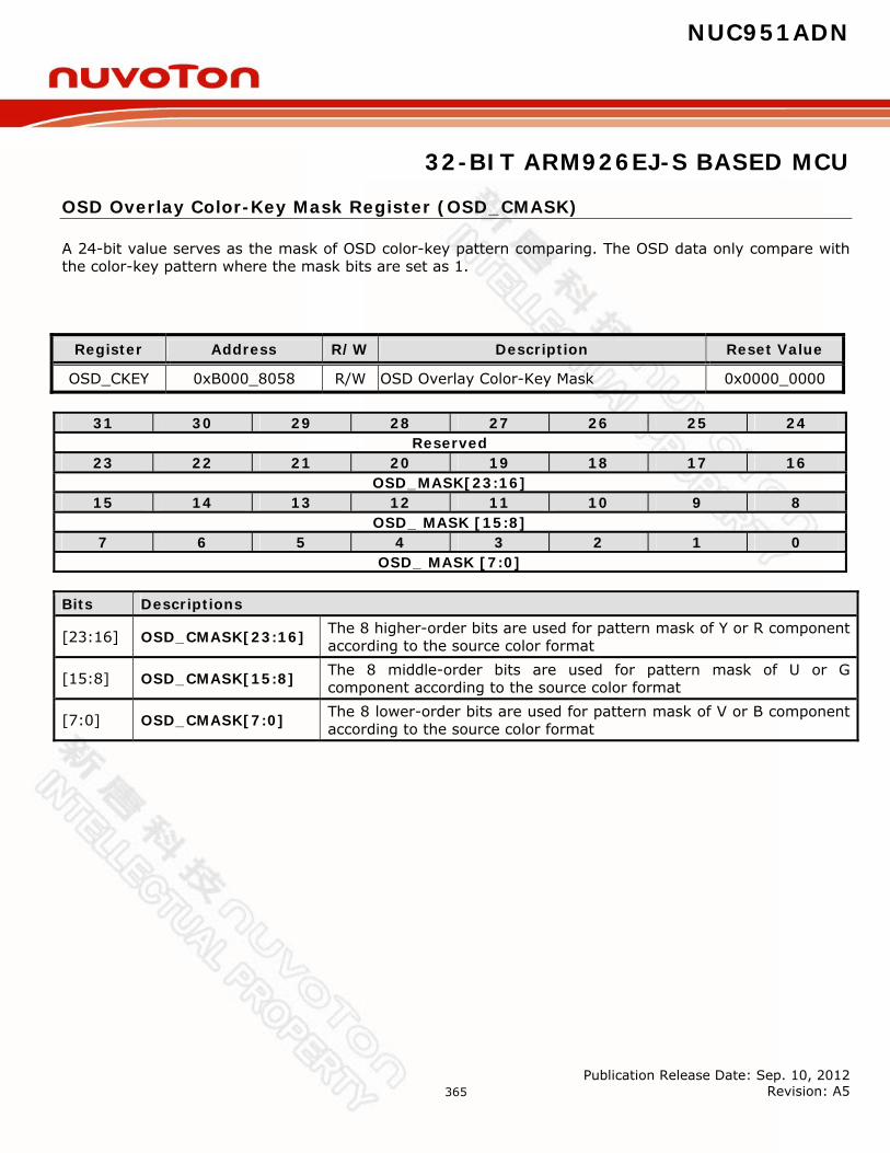
NUC951ADN
32-BIT ARM926EJ-S BASED MCU
Publication Release Date: Sep. 10, 2012 Revision: A5
365
OSD Overlay Color-Key Mask Register (OSD_CMASK)
A 24-bit value serves as the mask of OSD color-key pattern comparing. The OSD data only compare with the color-key pattern where the mask bits are set as 1.
Register Address R/W Description Reset Value
OSD_CKEY 0xB000_8058 R/W OSD Overlay Color-Key Mask 0x0000_0000
31 30 29 28 27 26 25 24 Reserved
23 22 21 20 19 18 17 16 OSD_MASK[23:16]
15 14 13 12 11 10 9 8 OSD_ MASK [15:8]
7 6 5 4 3 2 1 0 OSD_ MASK [7:0]
Bits Descriptions
[23:16] OSD_CMASK[23:16] The 8 higher-order bits are used for pattern mask of Y or R component according to the source color format
[15:8] OSD_CMASK[15:8] The 8 middle-order bits are used for pattern mask of U or G component according to the source color format
[7:0] OSD_CMASK[7:0] The 8 lower-order bits are used for pattern mask of V or B component according to the source color format
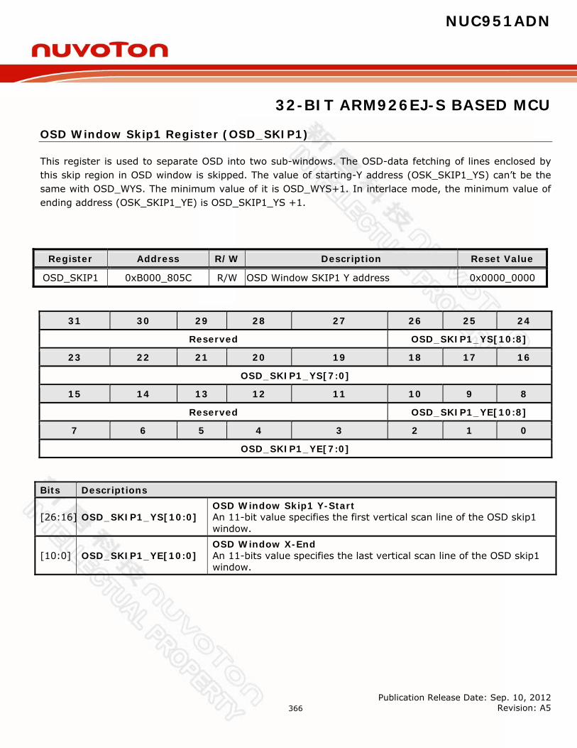
NUC951ADN
32-BIT ARM926EJ-S BASED MCU
Publication Release Date: Sep. 10, 2012 Revision: A5
366
OSD Window Skip1 Register (OSD_SKIP1)
This register is used to separate OSD into two sub-windows. The OSD-data fetching of lines enclosed by this skip region in OSD window is skipped. The value of starting-Y address (OSK_SKIP1_YS) can’t be the same with OSD_WYS. The minimum value of it is OSD_WYS+1. In interlace mode, the minimum value of ending address (OSK_SKIP1_YE) is OSD_SKIP1_YS +1.
Register Address R/W Description Reset Value
OSD_SKIP1 0xB000_805C R/W OSD Window SKIP1 Y address 0x0000_0000
31 30 29 28 27 26 25 24
Reserved OSD_SKIP1_YS[10:8]
23 22 21 20 19 18 17 16
OSD_SKIP1_YS[7:0]
15 14 13 12 11 10 9 8
Reserved OSD_SKIP1_YE[10:8]
7 6 5 4 3 2 1 0
OSD_SKIP1_YE[7:0] Bits Descriptions
[26:16] OSD_SKIP1_YS[10:0] OSD Window Skip1 Y-Start An 11-bit value specifies the first vertical scan line of the OSD skip1 window.
[10:0] OSD_SKIP1_YE[10:0] OSD Window X-End An 11-bits value specifies the last vertical scan line of the OSD skip1 window.

NUC951ADN
32-BIT ARM926EJ-S BASED MCU
Publication Release Date: Sep. 10, 2012 Revision: A5
367
OSD Window SKIP2 Register (OSD_SKIP2)
This register is used to separate OSD into two sub-windows. The OSD-data fetching of lines enclosed by this skip region in OSD window is skipped. The value of starting-Y address (OSK_SKIP2_YS) can’t be the same with OSD_WYS. The minimum value of it is OSD_WYS+1. In interlace mode, the minimum value of ending address (OSK_SKIP2_YE) is OSD_SKIP2_YS +1.
Register Address R/W Description Reset Value
OSD_SKIP2 0xB000_8060 R/W OSD Window SKIP2 Y address 0x0000_0000
31 30 29 28 27 26 25 24
Reserved OSD_SKIP2_YS[10:8]
23 22 21 20 19 18 17 16
OSD_SKIP2_YS[7:0]
15 14 13 12 11 10 9 8
Reserved OSD_SKIP2_YE[10:8]
7 6 5 4 3 2 1 0
OSD_SKIP2_YE[7:0] Bits Descriptions
[26:16] OSD_SKIP2_YS[10:0] OSD Window SKIP2 Y-Start An 11-bit value specifies the first vertical scan line of the OSD SKIP2 window.
[10:0] OSD_SKIP2_YE[10:0] OSD Window X-End An 11-bits value specifies the last vertical scan line of the OSD SKIP2 window.
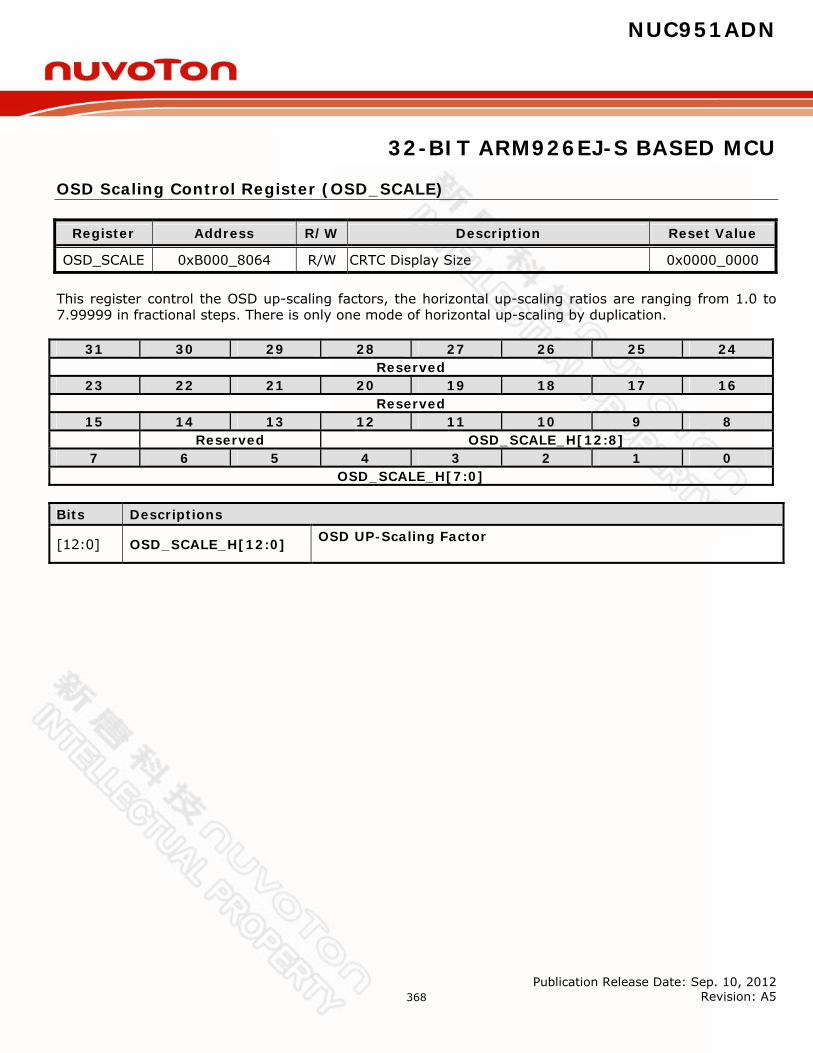
NUC951ADN
32-BIT ARM926EJ-S BASED MCU
Publication Release Date: Sep. 10, 2012 Revision: A5
368
OSD Scaling Control Register (OSD_SCALE)
Register Address R/W Description Reset Value
OSD_SCALE 0xB000_8064 R/W CRTC Display Size 0x0000_0000 This register control the OSD up-scaling factors, the horizontal up-scaling ratios are ranging from 1.0 to 7.99999 in fractional steps. There is only one mode of horizontal up-scaling by duplication.
31 30 29 28 27 26 25 24 Reserved
23 22 21 20 19 18 17 16 Reserved
15 14 13 12 11 10 9 8 Reserved OSD_SCALE_H[12:8]
7 6 5 4 3 2 1 0 OSD_SCALE_H[7:0]
Bits Descriptions
[12:0] OSD_SCALE_H[12:0] OSD UP-Scaling Factor
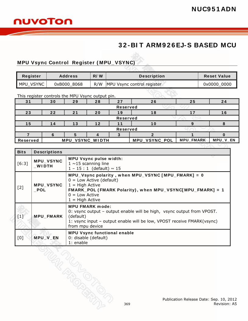
NUC951ADN
32-BIT ARM926EJ-S BASED MCU
Publication Release Date: Sep. 10, 2012 Revision: A5
369
MPU Vsync Control Register (MPU_VSYNC)
Register Address R/W Description Reset Value
MPU_VSYNC 0xB000_8068 R/W MPU Vsync control register 0x0000_0000 This register controls the MPU Vsync output pin.
31 30 29 28 27 26 25 24 Reserved
23 22 21 20 19 18 17 16 Reserved
15 14 13 12 11 10 9 8 Reserved
7 6 5 4 3 2 1 0 Reserved MPU_VSYNC_WIDTH MPU_VSYNC_POL MPU_FMARK MPU_V_EN Bits Descriptions
[6:3] MPU_VSYNC _WIDTH
MPU Vsync pulse width: 1 ~15 scanning line 1 – 15 : 1 (default) ~ 15
[2] MPU_VSYNC _POL
MPU_Vsync polarity , when MPU_VSYNC [MPU_FMARK] = 0 0 = Low Active (default) 1 = High Active FMARK_POL (FMARK Polarity), when MPU_VSYNC[MPU_FMARK] = 1 0 = Low Active 1 = High Active
[1] MPU_FMARK
MPU FMARK mode: 0: vsync output – output enable will be high, vsync output from VPOST. (default) 1: vsync input – output enable will be low, VPOST receive FMARK(vsync) from mpu device
[0] MPU_V_EN MPU Vsync functional enable 0: disable (default) 1: enable
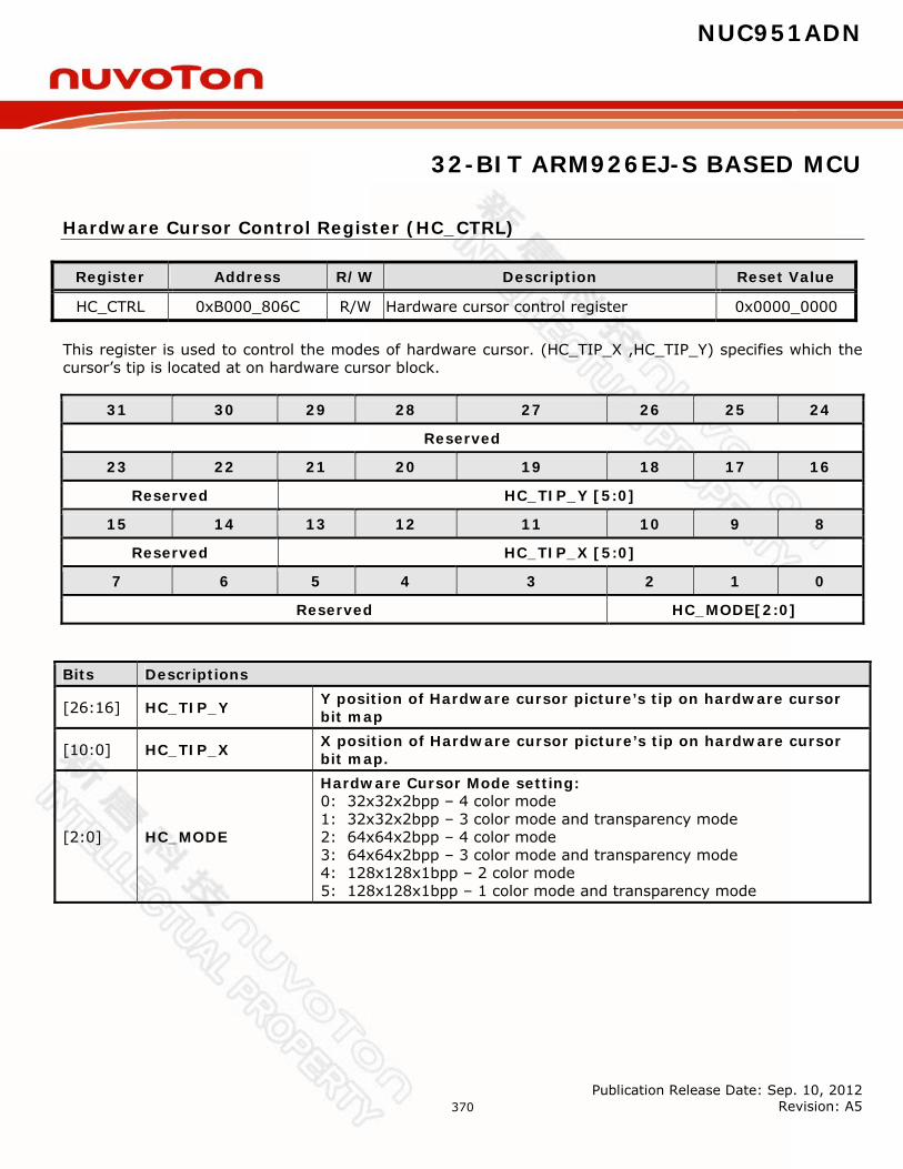
NUC951ADN
32-BIT ARM926EJ-S BASED MCU
Publication Release Date: Sep. 10, 2012 Revision: A5
370
Hardware Cursor Control Register (HC_CTRL)
Register Address R/W Description Reset Value
HC_CTRL 0xB000_806C R/W Hardware cursor control register 0x0000_0000 This register is used to control the modes of hardware cursor. (HC_TIP_X ,HC_TIP_Y) specifies which the cursor’s tip is located at on hardware cursor block.
31 30 29 28 27 26 25 24
Reserved
23 22 21 20 19 18 17 16
Reserved HC_TIP_Y [5:0]
15 14 13 12 11 10 9 8
Reserved HC_TIP_X [5:0]
7 6 5 4 3 2 1 0
Reserved HC_MODE[2:0] Bits Descriptions
[26:16] HC_TIP_Y Y position of Hardware cursor picture’s tip on hardware cursor bit map
[10:0] HC_TIP_X X position of Hardware cursor picture’s tip on hardware cursor bit map.
[2:0] HC_MODE
Hardware Cursor Mode setting: 0: 32x32x2bpp – 4 color mode 1: 32x32x2bpp – 3 color mode and transparency mode 2: 64x64x2bpp – 4 color mode 3: 64x64x2bpp – 3 color mode and transparency mode 4: 128x128x1bpp – 2 color mode 5: 128x128x1bpp – 1 color mode and transparency mode
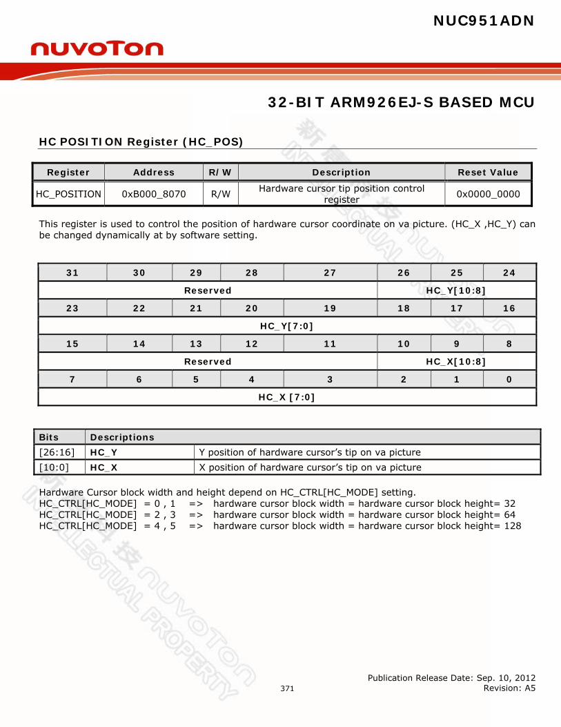
NUC951ADN
32-BIT ARM926EJ-S BASED MCU
Publication Release Date: Sep. 10, 2012 Revision: A5
371
HC POSITION Register (HC_POS)
Register Address R/W Description Reset Value
HC_POSITION 0xB000_8070 R/W Hardware cursor tip position control register 0x0000_0000
This register is used to control the position of hardware cursor coordinate on va picture. (HC_X ,HC_Y) can be changed dynamically at by software setting.
31 30 29 28 27 26 25 24
Reserved HC_Y[10:8]
23 22 21 20 19 18 17 16
HC_Y[7:0]
15 14 13 12 11 10 9 8
Reserved HC_X[10:8]
7 6 5 4 3 2 1 0
HC_X [7:0] Bits Descriptions [26:16] HC_Y Y position of hardware cursor’s tip on va picture [10:0] HC_X X position of hardware cursor’s tip on va picture Hardware Cursor block width and height depend on HC_CTRL[HC_MODE] setting. HC_CTRL[HC_MODE] = 0 , 1 => hardware cursor block width = hardware cursor block height= 32 HC_CTRL[HC_MODE] = 2 , 3 => hardware cursor block width = hardware cursor block height= 64 HC_CTRL[HC_MODE] = 4 , 5 => hardware cursor block width = hardware cursor block height= 128
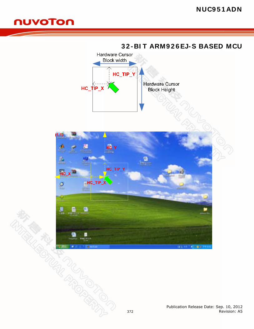
NUC951ADN
32-BIT ARM926EJ-S BASED MCU
Publication Release Date: Sep. 10, 2012 Revision: A5
372
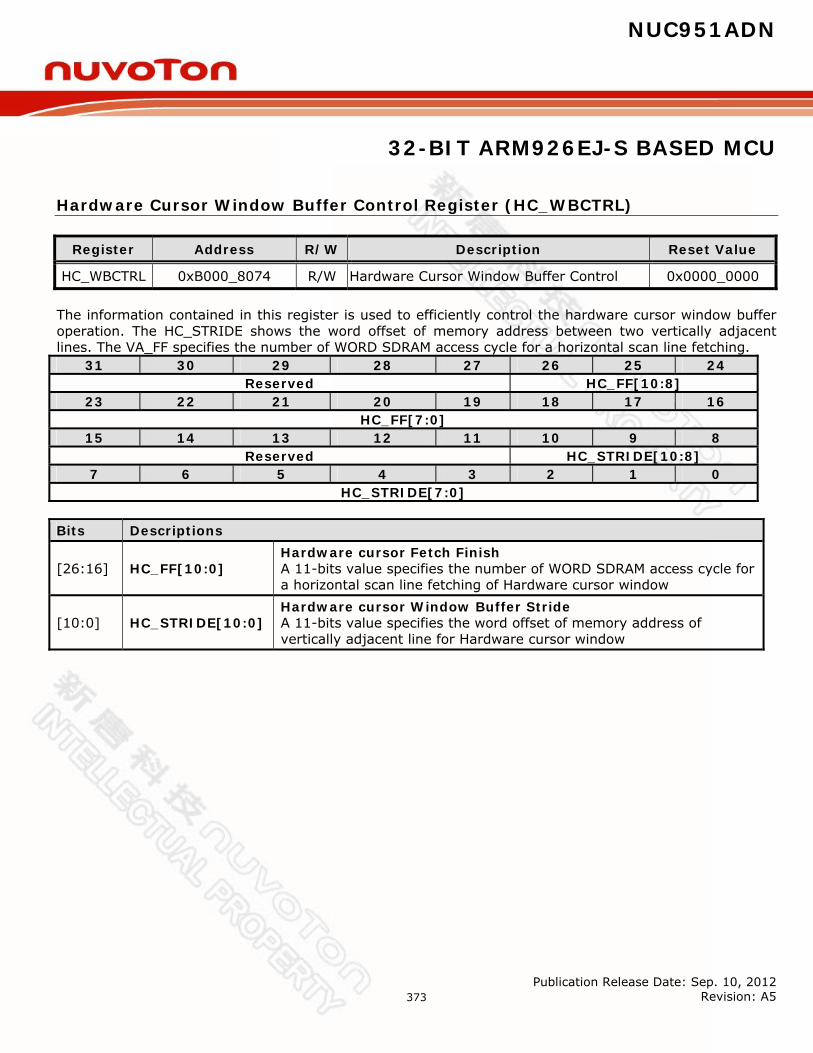
NUC951ADN
32-BIT ARM926EJ-S BASED MCU
Publication Release Date: Sep. 10, 2012 Revision: A5
373
Hardware Cursor Window Buffer Control Register (HC_WBCTRL)
Register Address R/W Description Reset Value
HC_WBCTRL 0xB000_8074 R/W Hardware Cursor Window Buffer Control 0x0000_0000 The information contained in this register is used to efficiently control the hardware cursor window buffer operation. The HC_STRIDE shows the word offset of memory address between two vertically adjacent lines. The VA_FF specifies the number of WORD SDRAM access cycle for a horizontal scan line fetching.
31 30 29 28 27 26 25 24 Reserved HC_FF[10:8]
23 22 21 20 19 18 17 16 HC_FF[7:0]
15 14 13 12 11 10 9 8 Reserved HC_STRIDE[10:8]
7 6 5 4 3 2 1 0 HC_STRIDE[7:0]
Bits Descriptions
[26:16] HC_FF[10:0] Hardware cursor Fetch Finish A 11-bits value specifies the number of WORD SDRAM access cycle for a horizontal scan line fetching of Hardware cursor window
[10:0] HC_STRIDE[10:0] Hardware cursor Window Buffer Stride A 11-bits value specifies the word offset of memory address of vertically adjacent line for Hardware cursor window

NUC951ADN
32-BIT ARM926EJ-S BASED MCU
Publication Release Date: Sep. 10, 2012 Revision: A5
374
HC BADDR Register (HC_BADDR)
Register Address R/W Description Reset Value
HC_BADDR 0xB000_8078 R/W Hardware cursor memory base address register 0x0000_0000
This register is used to control the starting memory address of the frame buffer for Hardware cursor data stream.
31 30 29 28 27 26 25 24
HC_BADDR[31:24]
23 22 21 20 19 18 17 16
HC_BADDR[23:16]
15 14 13 12 11 10 9 8
HC_BADDR[15:8]
7 6 5 4 3 2 1 0
HC_BADDR[7:0] Bits Descriptions
[31:0] HC_BADDR
Starting memory address of the frame buffer for Hardware cursor data stream The value of this register represents the starting memory address of the frame buffer
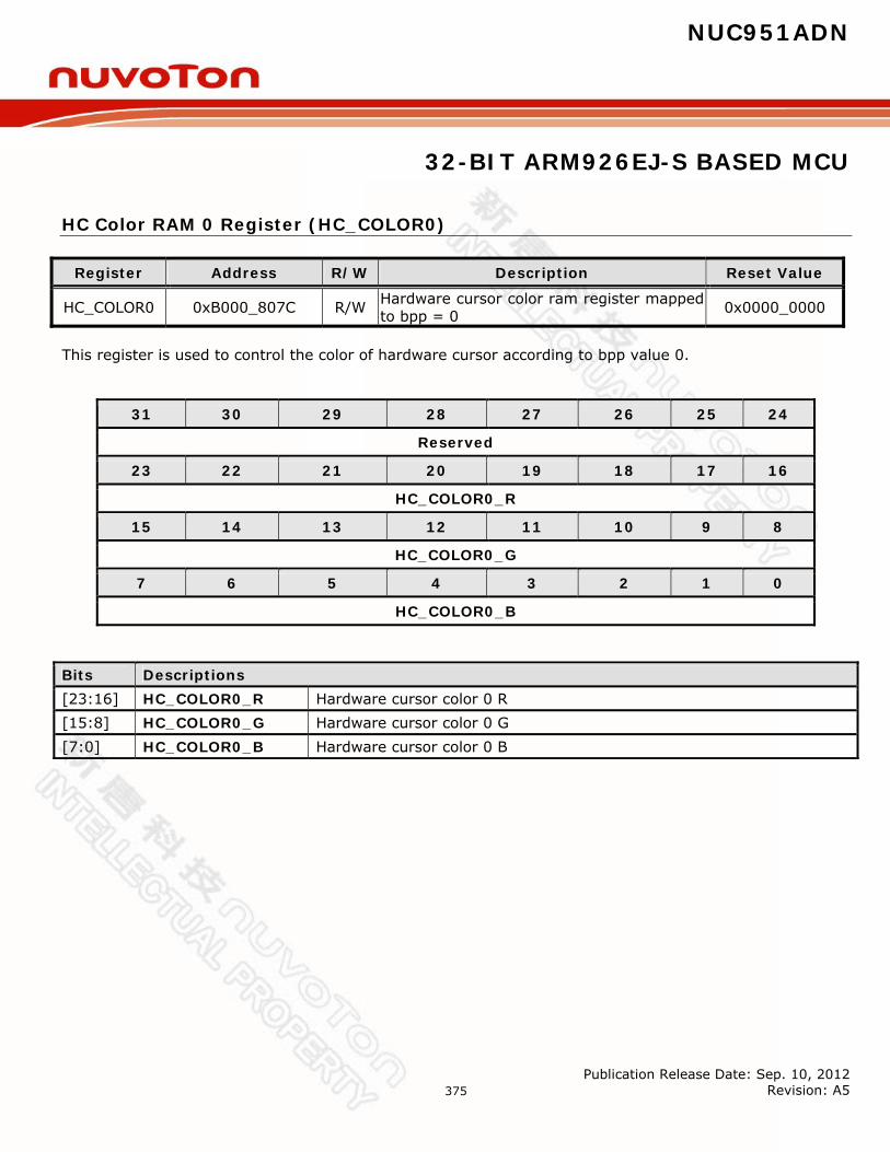
NUC951ADN
32-BIT ARM926EJ-S BASED MCU
Publication Release Date: Sep. 10, 2012 Revision: A5
375
HC Color RAM 0 Register (HC_COLOR0)
Register Address R/W Description Reset Value
HC_COLOR0 0xB000_807C R/W Hardware cursor color ram register mapped to bpp = 0 0x0000_0000
This register is used to control the color of hardware cursor according to bpp value 0.
31 30 29 28 27 26 25 24
Reserved
23 22 21 20 19 18 17 16
HC_COLOR0_R
15 14 13 12 11 10 9 8
HC_COLOR0_G
7 6 5 4 3 2 1 0
HC_COLOR0_B Bits Descriptions [23:16] HC_COLOR0_R Hardware cursor color 0 R [15:8] HC_COLOR0_G Hardware cursor color 0 G [7:0] HC_COLOR0_B Hardware cursor color 0 B
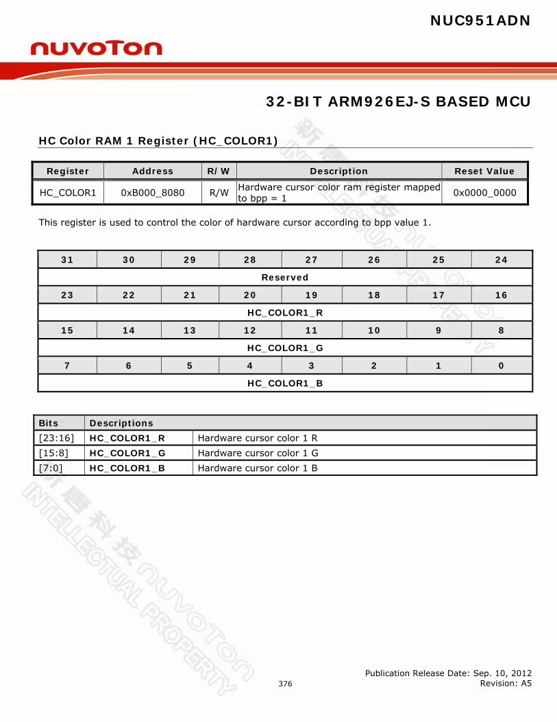
NUC951ADN
32-BIT ARM926EJ-S BASED MCU
Publication Release Date: Sep. 10, 2012 Revision: A5
376
HC Color RAM 1 Register (HC_COLOR1)
Register Address R/W Description Reset Value
HC_COLOR1 0xB000_8080 R/W Hardware cursor color ram register mapped to bpp = 1 0x0000_0000
This register is used to control the color of hardware cursor according to bpp value 1.
31 30 29 28 27 26 25 24
Reserved
23 22 21 20 19 18 17 16
HC_COLOR1_R
15 14 13 12 11 10 9 8
HC_COLOR1_G
7 6 5 4 3 2 1 0
HC_COLOR1_B Bits Descriptions [23:16] HC_COLOR1_R Hardware cursor color 1 R [15:8] HC_COLOR1_G Hardware cursor color 1 G [7:0] HC_COLOR1_B Hardware cursor color 1 B

NUC951ADN
32-BIT ARM926EJ-S BASED MCU
Publication Release Date: Sep. 10, 2012 Revision: A5
377
HC Color RAM 2 Register (HC_COLOR2)
Register Address R/W Description Reset Value
HC_COLOR2 0xB000_8084 R/W Hardware cursor color ram register mapped to bpp = 2 0x0000_0000
This register is used to control the color of hardware cursor according to bpp value 2.
31 30 29 28 27 26 25 24
Reserved
23 22 21 20 19 18 17 16
HC_COLOR2_R
15 14 13 12 11 10 9 8
HC_COLOR2_G
7 6 5 4 3 2 1 0
HC_COLOR2_B Bits Descriptions [23:16] HC_COLOR2_B Hardware cursor color 2 R [15:8] HC_COLOR2_G Hardware cursor color 2 G [7:0] HC_COLOR2_R Hardware cursor color 2 B

NUC951ADN
32-BIT ARM926EJ-S BASED MCU
Publication Release Date: Sep. 10, 2012 Revision: A5
378
HC Color RAM 3 Register (HC_COLOR3)
Register Address R/W Description Reset Value
HC_COLOR3 0xB000_8088 R/W Hardware cursor color ram register mapped to bpp = 3 0x0000_0000
This register is used to control the color of hardware cursor according to bpp value 3. When transparency is enabling, this color ram will be ignored.
31 30 29 28 27 26 25 24
Reserved
23 22 21 20 19 18 17 16
HC_COLOR3_R
15 14 13 12 11 10 9 8
HC_COLOR3_G
7 6 5 4 3 2 1 0
HC_COLOR3_B Bits Descriptions
[23:16] HC_COLOR3_R Hardware cursor color 3 R. When transparency is enabling, this color ram will be ignored.
[15:8] HC_COLOR3_G Hardware cursor color 3 G. When transparency is enabling, this color ram will be ignored.
[7:0] HC_COLOR3_B Hardware cursor color 3 B. When transparency is enabling, this color ram will be ignored.
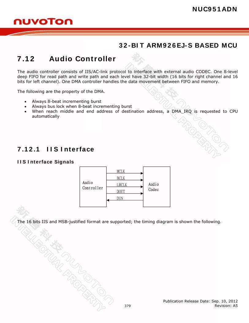
NUC951ADN
32-BIT ARM926EJ-S BASED MCU
Publication Release Date: Sep. 10, 2012 Revision: A5
379
7.12 Audio Controller The audio controller consists of IIS/AC-link protocol to interface with external audio CODEC. One 8-level deep FIFO for read path and write path and each level have 32-bit width (16 bits for right channel and 16 bits for left channel). One DMA controller handles the data movement between FIFO and memory. The following are the property of the DMA.
Always 8-beat incrementing burst Always bus lock when 8-beat incrementing burst When reach middle and end address of destination address, a DMA_IRQ is requested to CPU
automatically
7.12.1 IIS Interface
IIS Interface Signals The 16 bits IIS and MSB-justified format are supported; the timing diagram is shown the following.
Audio
Controller
Audio
Codec
MCLK
BCLK
LRCLK
DOUT
DIN
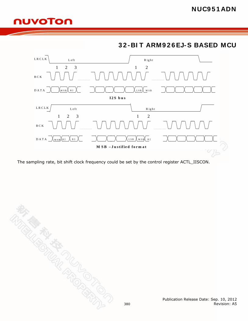
NUC951ADN
32-BIT ARM926EJ-S BASED MCU
Publication Release Date: Sep. 10, 2012 Revision: A5
380
L R C L K
B C K
D A T A
L e f t R ig h t
1 2 3
M S B B 2
1 2
L S B M S B
I 2 S b u s
L R C L K
B C K
D A T A
L e f t R ig h t
1 2 3
B 2 B 3
1 2
M S B B 2
M S B – J u s t if ie d f o r m a t
M S B L S B
The sampling rate, bit shift clock frequency could be set by the control register ACTL_IISCON.
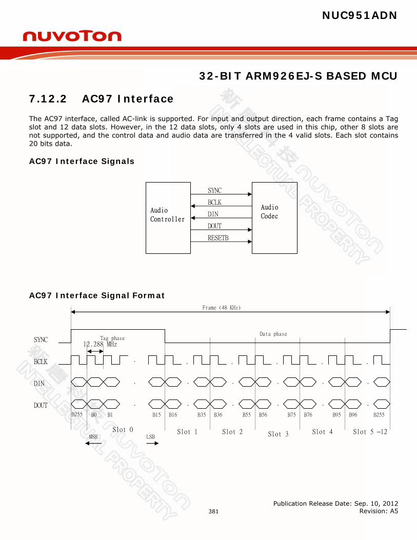
NUC951ADN
32-BIT ARM926EJ-S BASED MCU
Publication Release Date: Sep. 10, 2012 Revision: A5
381
7.12.2 AC97 Interface The AC97 interface, called AC-link is supported. For input and output direction, each frame contains a Tag slot and 12 data slots. However, in the 12 data slots, only 4 slots are used in this chip, other 8 slots are not supported, and the control data and audio data are transferred in the 4 valid slots. Each slot contains 20 bits data. AC97 Interface Signals
AC97 Interface Signal Format
Audio
Controller
Audio
Codec
SYNC
BCLK
DIN
DOUT
RESETB
. . . . .
......
.
......
SYNC
BCLK
DIN
DOUT
Tag phase Data phase
Slot 0 Slot 1 Slot 2 Slot 3 Slot 4 Slot 5 –12
Frame (48 KHz)
12.288 MHz
B255 B0 B1 B15 B16 B35
MSB LSB
B36 B55 B56 B75 B76 B95 B96 B255
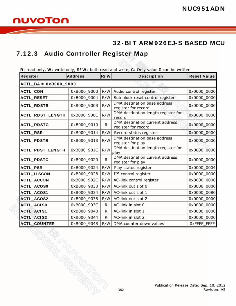
NUC951ADN
32-BIT ARM926EJ-S BASED MCU
Publication Release Date: Sep. 10, 2012 Revision: A5
382
7.12.3 Audio Controller Register Map
R: read only, W: write only, R/W: both read and write, C: Only value 0 can be written Register Address R/W Description Reset Value
ACTL_BA = 0xB000_9000
ACTL_CON 0xB000_9000 R/W Audio control register 0x0000_0000 ACTL_RESET 0xB000_9004 R/W Sub block reset control register 0x0000_0000
ACTL_RDSTB 0xB000_9008 R/W DMA destination base address register for record 0x0000_0000
ACTL_RDST_LENGTH 0xB000_900C R/W DMA destination length register for record 0x0000_0000
ACTL_RDSTC 0xB000_9010 R DMA destination current address register for record 0x0000_0000
ACTL_RSR 0xB000_9014 R/W Record status register 0x0000_0000
ACTL_PDSTB 0xB000_9018 R/W DMA destination base address register for play 0x0000_0000
ACTL_PDST_LENGTH 0xB000_901C R/W DMA destination length register for play 0x0000_0000
ACTL_PDSTC 0xB000_9020 R DMA destination current address register for play 0x0000_0000
ACTL_PSR 0xB000_9024 R/W Play status register 0x0000_0004 ACTL_IISCON 0xB000_9028 R/W IIS control register 0x0000_0000 ACTL_ACCON 0xB000_902C R/W AC-link control register 0x0000_0000 ACTL_ACOS0 0xB000_9030 R/W AC-link out slot 0 0x0000_0000 ACTL_ACOS1 0xB000_9034 R/W AC-link out slot 1 0x0000_0080 ACTL_ACOS2 0xB000_9038 R/W AC-link out slot 2 0x0000_0000 ACTL_ACIS0 0xB000_903C R AC-link in slot 0 0x0000_0000 ACTL_ACIS1 0xB000_9040 R AC-link in slot 1 0x0000_0000 ACTL_ACIS2 0xB000_9044 R AC-link in slot 2 0x0000_0000 ACTL_COUNTER 0xB000_9048 R/W DMA counter down values 0xFFFF_FFFF
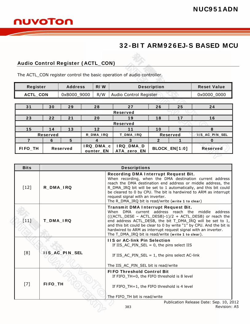
NUC951ADN
32-BIT ARM926EJ-S BASED MCU
Publication Release Date: Sep. 10, 2012 Revision: A5
383
Audio Control Register (ACTL_CON)
The ACTL_CON register control the basic operation of audio controller.
Register Address R/W Description Reset Value
ACTL_CON 0xB000_9000 R/W Audio Control Register 0x0000_0000
31 30 29 28 27 26 25 24 Reserved
23 22 21 20 19 18 17 16 Reserved
15 14 13 12 11 10 9 8 Reserved R_DMA_IRQ T_DMA_IRQ Reserved IIS_AC_PIN_SEL
7 6 5 4 3 2 1 0
FIFO_TH Reserved IRQ_DMA_counter_EN
IRQ_DMA_DATA_zero_EN BLOCK_EN[1:0] Reserved
Bits Descriptions
[12] R_DMA_IRQ
Recording DMA Interrupt Request Bit. When recording, when the DMA destination current address reach the DMA destination end address or middle address, the R_DMA_IRQ bit will be set to 1 automatically, and this bit could be cleared to 0 by CPU. The bit is hardwired to ARM as interrupt request signal with an inverter. The R_DMA_IRQ bit is read/write (write 1 to clear)
[11] T_DMA_IRQ
Transmit DMA Interrupt Request Bit. When DMA current address reach the middle address (((ACTL_DESE – ACTL_DESB)-1)/2 + ACTL_DESB) or reach the end address ACTL_DESB, the bit T_DMA_IRQ will be set to 1, and this bit could be clear to 0 by write “1” by CPU. And the bit is hardwired to ARM as interrupt request signal with an inverter. The T_DMA_IRQ bit is read/write (write 1 to clear).
[8] IIS_AC_PIN_SEL
IIS or AC-link Pin Selection If IIS_AC_PIN_SEL = 0, the pins select IIS
If IIS_AC_PIN_SEL = 1, the pins select AC-link
The IIS_AC_PIN_SEL bit is read/write
[7] FIFO_TH
FIFO Threshold Control Bit If FIFO_TH=0, the FIFO threshold is 8 level
If FIFO_TH=1, the FIFO threshold is 4 level
The FIFO_TH bit is read/write
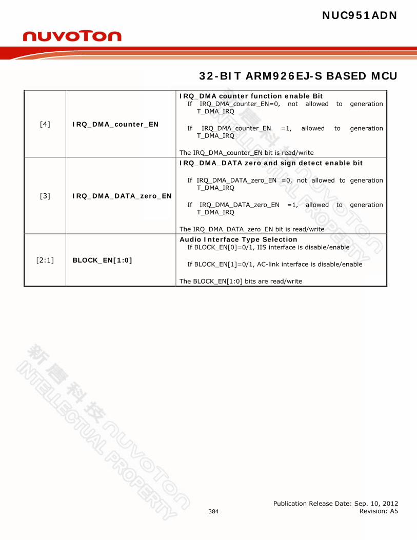
NUC951ADN
32-BIT ARM926EJ-S BASED MCU
Publication Release Date: Sep. 10, 2012 Revision: A5
384
[4] IRQ_DMA_counter_EN
IRQ_DMA counter function enable Bit If IRQ_DMA_counter_EN=0, not allowed to generation
T_DMA_IRQ
If IRQ_DMA_counter_EN =1, allowed to generation T_DMA_IRQ
The IRQ_DMA_counter_EN bit is read/write
[3] IRQ_DMA_DATA_zero_EN
IRQ_DMA_DATA zero and sign detect enable bit
If IRQ_DMA_DATA_zero_EN =0, not allowed to generation T_DMA_IRQ
If IRQ_DMA_DATA_zero_EN =1, allowed to generation T_DMA_IRQ
The IRQ_DMA_DATA_zero_EN bit is read/write
[2:1] BLOCK_EN[1:0]
Audio Interface Type Selection If BLOCK_EN[0]=0/1, IIS interface is disable/enable
If BLOCK_EN[1]=0/1, AC-link interface is disable/enable
The BLOCK_EN[1:0] bits are read/write

NUC951ADN
32-BIT ARM926EJ-S BASED MCU
Publication Release Date: Sep. 10, 2012 Revision: A5
385
Sub-block Reset Control Register (ACTL_RESET)
The value of ACTL_RESET register controls the reset operation in each sub block.
Register Address R/W Description Reset Value
ACTL_RESET 0xB000_9004 R/W Sub block reset control 0x0000_0000
Bits Descriptions
[16] ACTL_RESET
Audio Controller Reset Control Bit If ACTL_RESET = 1, the whole audio controller is reset
If ACTL_RESET = 0, the audio controller is normal operation
The ACTL_RESET bit is read/write
[15:14] RECORD_SINGLE
Record Single/Dual Channel Select Bits If RECORD_SINGLE[1:0]=11, the record is dual channel
If RECORD_SINGLE[1:0]=01, the record only select left channel
If RECORD_SINGLE[1:0]=10, the record only select right channel
RECORD_SINGLE[1:0]=00 is reserved
Note that, when ADC is selected as record path, it only supported left channel record. The PLAY_SINGLE[1:0] bits are read/write
[13:12] PLAY_SINGLE
Playback Single/Dual Channel Select Bits If PLAY_SINGLE[1:0]=11, the playback is in stereo mode
If PLAY_SINGLE[1:0]=10, the playback is in mono mode
31 30 29 28 27 26 25 24
Reserved
23 22 21 20 19 18 17 16
Reserved ACTL_RESET
15 14 13 12 11 10 9 8
RECORD_SINGLE PLAY_SINGLE Reserved AC_RECORD
7 6 5 4 3 2 1 0
AC_PLAY IIS_RECORD IIS_PLAY DMA_counter_EN
DMA_DATA_zero_EN Reserved AC_RESET IIS_RESET
NUC951ADN
32-BIT ARM926EJ-S BASED MCU
Publication Release Date: Sep. 10, 2012 Revision: A5
386
PLAY_SINGLE[1:0]= 00 & 01 is reserved
The PLAY_SINGLE[1:0] bits are read/write

NUC951ADN
32-BIT ARM926EJ-S BASED MCU
Publication Release Date: Sep. 10, 2012 Revision: A5
387
[8] AC_RECORD
AC link Record Control Bit If AC_RECORD=0, the record path of AC link is disable
If AC_RECORD=1, the record path of AC link is enable
The AC_RECORD bit is read/write
[7] AC_PLAY
AC link Playback Control Bit If AC_PLAY=0, the playback path of AC link is disable
If AC_PLAY=1, the playback path of AC link is enable
The AC_PLAY bit is read/write
[6] IIS_RECORD
IIS Record Control Bit If IIS_RECORD=0, the record path of IIS is disable
If IIS_RECORD=1, the record path of IIS is enable
The IIS_RECORD bit is read/write
[5] IIS_PLAY
IIS Playback Control Bit If IIS_PLAY=0, the playback path of IIS is disable
If IIS_PLAY=1, the playback path of IIS is enable
The IIS_PLAY bit is read/write
[4] DMA_counter_EN
DMA counter function enable Bit If DMA_counter_EN=0, not enable DMA counter function
If DMA_counter_EN =1, enable DMA counter function
The DMA_counter_EN bit is read/write
[3] DMA_DATA_zero_EN
DMA_DATA zero and sign detect enable bit
If DMA_DATA_zero_EN =0, not enable DMA_DATA zero and sign detect function
If DMA_DATA_zero_EN =1, enable DMA_DATA zero and sign detect function
The DMA_DATA_zero_EN bit is read/write
[1] AC_RESET
AC link Sub Block RESET Control Bit If AC_RESET=0, release the AC link function block from reset mode
If AC_RESET=1, force the AC link function block to reset mode
The AC_RESET bit is read/write [0] IIS_RESET IIS Sub Block RESET Control Bit

NUC951ADN
32-BIT ARM926EJ-S BASED MCU
Publication Release Date: Sep. 10, 2012 Revision: A5
388
If IIS_RESET=0, release the IIS function block from reset mode
If IIS_RESET=1, force the IIS function block to reset mode
The IIS_RESET bit is read/write
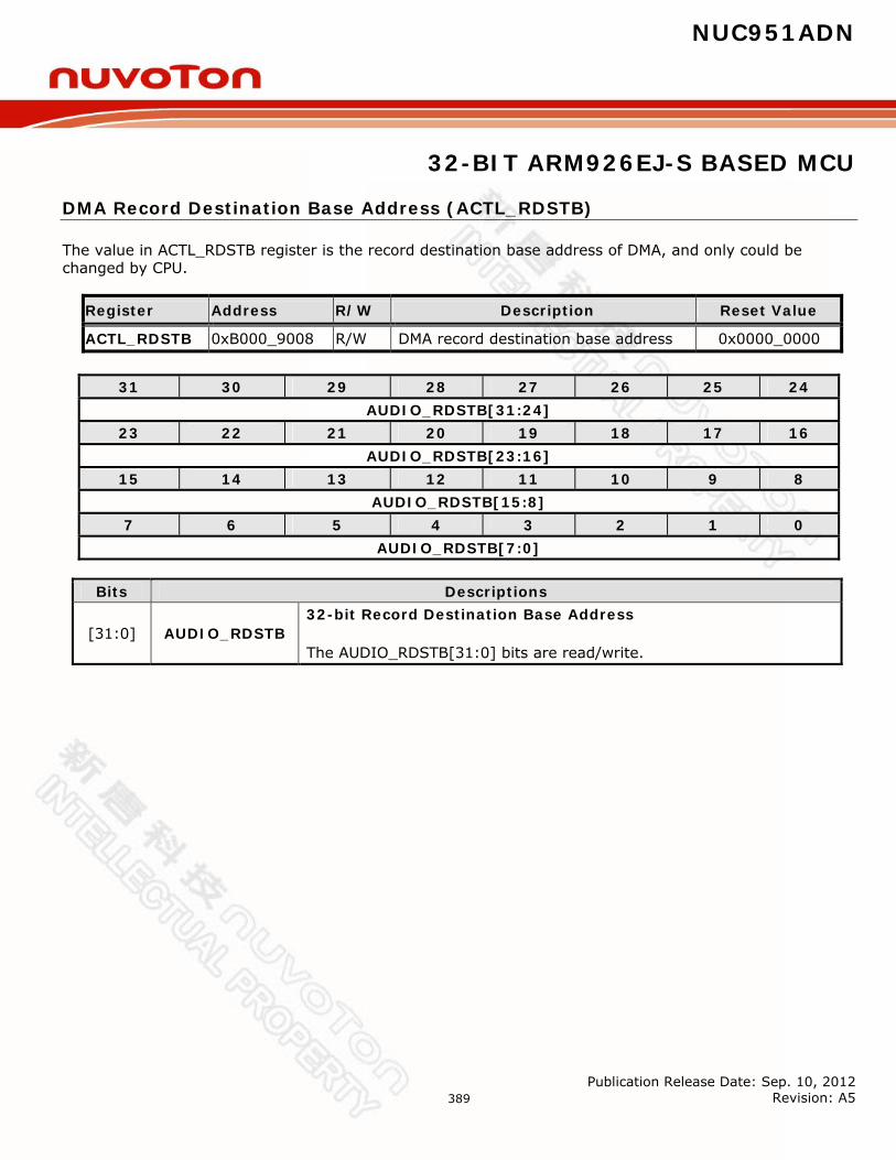
NUC951ADN
32-BIT ARM926EJ-S BASED MCU
Publication Release Date: Sep. 10, 2012 Revision: A5
389
DMA Record Destination Base Address (ACTL_RDSTB)
The value in ACTL_RDSTB register is the record destination base address of DMA, and only could be changed by CPU.
Register Address R/W Description Reset Value
ACTL_RDSTB 0xB000_9008 R/W DMA record destination base address 0x0000_0000
Bits Descriptions
[31:0] AUDIO_RDSTB 32-bit Record Destination Base Address
The AUDIO_RDSTB[31:0] bits are read/write.
31 30 29 28 27 26 25 24 AUDIO_RDSTB[31:24]
23 22 21 20 19 18 17 16 AUDIO_RDSTB[23:16]
15 14 13 12 11 10 9 8 AUDIO_RDSTB[15:8]
7 6 5 4 3 2 1 0 AUDIO_RDSTB[7:0]
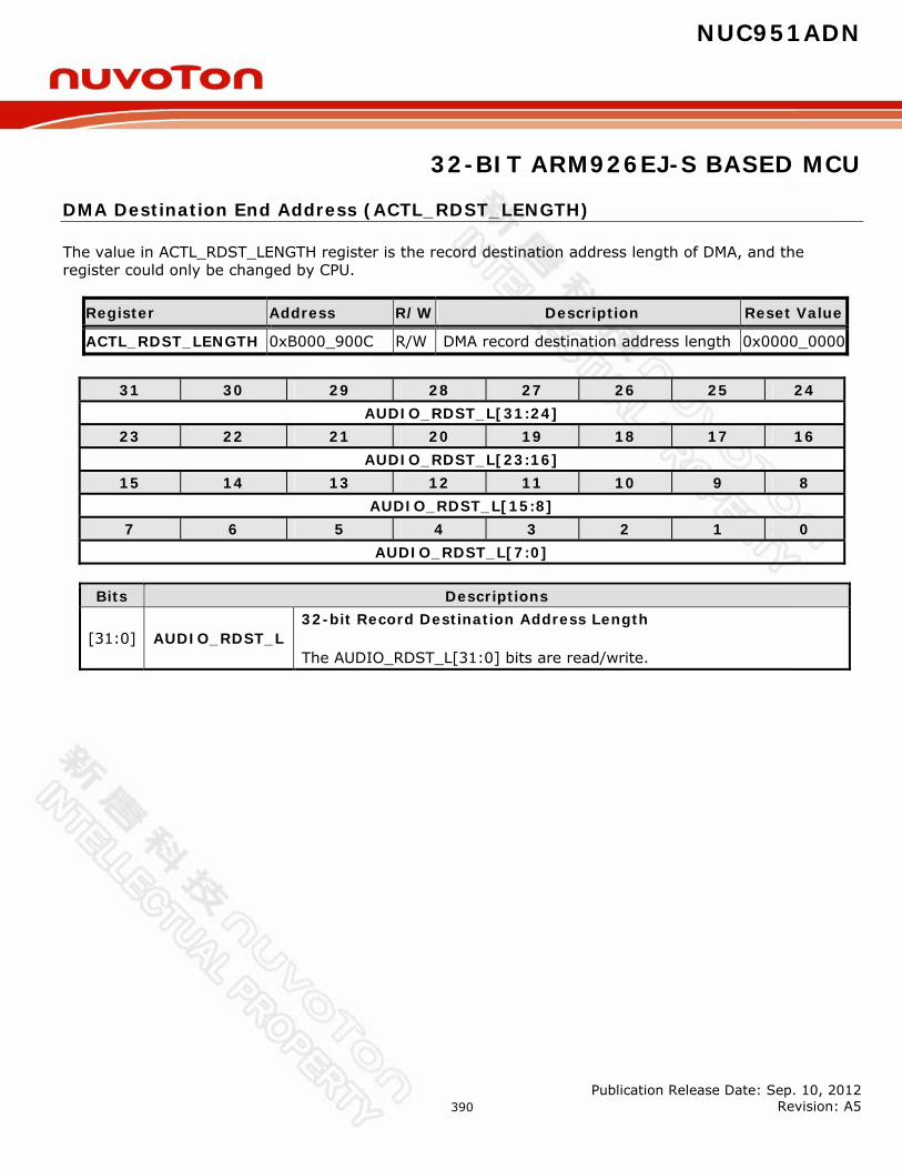
NUC951ADN
32-BIT ARM926EJ-S BASED MCU
Publication Release Date: Sep. 10, 2012 Revision: A5
390
DMA Destination End Address (ACTL_RDST_LENGTH)
The value in ACTL_RDST_LENGTH register is the record destination address length of DMA, and the register could only be changed by CPU.
Register Address R/W Description Reset Value
ACTL_RDST_LENGTH 0xB000_900C R/W DMA record destination address length 0x0000_0000
Bits Descriptions
[31:0] AUDIO_RDST_L 32-bit Record Destination Address Length
The AUDIO_RDST_L[31:0] bits are read/write.
31 30 29 28 27 26 25 24 AUDIO_RDST_L[31:24]
23 22 21 20 19 18 17 16 AUDIO_RDST_L[23:16]
15 14 13 12 11 10 9 8 AUDIO_RDST_L[15:8]
7 6 5 4 3 2 1 0 AUDIO_RDST_L[7:0]

NUC951ADN
32-BIT ARM926EJ-S BASED MCU
Publication Release Date: Sep. 10, 2012 Revision: A5
391
DMA Destination Current Address (ACTL_RDSTC)
The value in ACTL_RDSTC is the DMA record destination current address; this register could only be read by CPU.
Register Address R/W Description Reset Value
ACTL_RDSTC 0xB000_9010 R DMA record destination current address 0x0000_0000
Bits Descriptions
[31:0] AUDIO_RDSTC 32-bit Record Destination Current Address
The AUDIO_RDSTC[31:0] bits are read only.
31 30 29 28 27 26 25 24 AUDIO_RDSTC[31:24]
23 22 21 20 19 18 17 16 AUDIO_RDSTC[23:16]
15 14 13 12 11 10 9 8 AUDIO_RDSTC[15:8]
7 6 5 4 3 2 1 0 AUDIO_RDSTC[7:0]
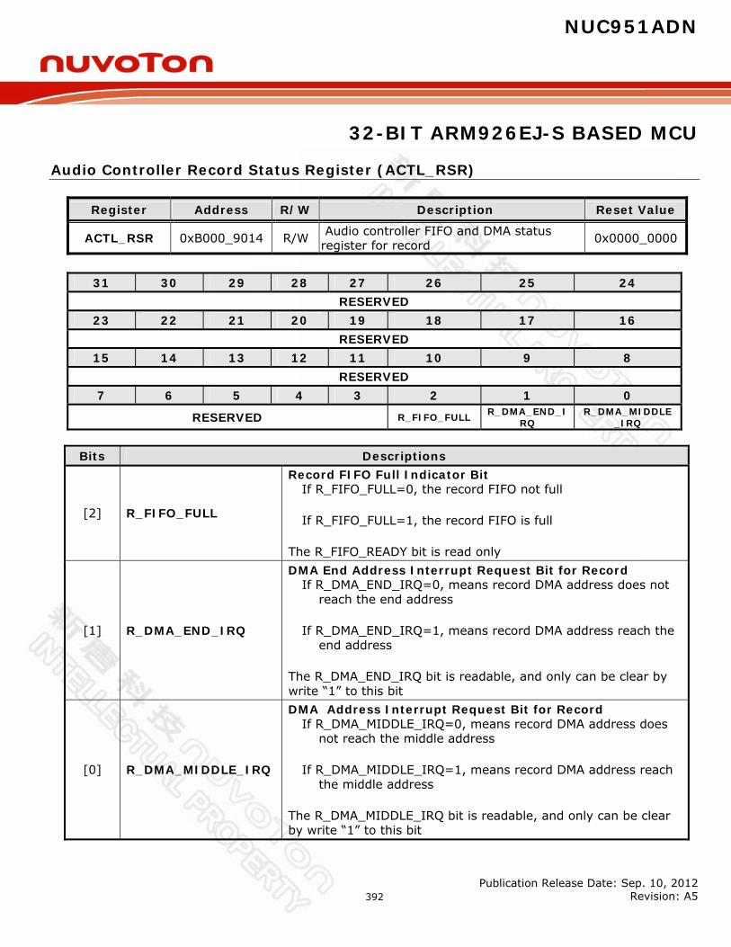
NUC951ADN
32-BIT ARM926EJ-S BASED MCU
Publication Release Date: Sep. 10, 2012 Revision: A5
392
Audio Controller Record Status Register (ACTL_RSR)
Register Address R/W Description Reset Value
ACTL_RSR 0xB000_9014 R/W Audio controller FIFO and DMA status register for record 0x0000_0000
Bits Descriptions
[2] R_FIFO_FULL
Record FIFO Full Indicator Bit If R_FIFO_FULL=0, the record FIFO not full
If R_FIFO_FULL=1, the record FIFO is full
The R_FIFO_READY bit is read only
[1] R_DMA_END_IRQ
DMA End Address Interrupt Request Bit for Record If R_DMA_END_IRQ=0, means record DMA address does not
reach the end address
If R_DMA_END_IRQ=1, means record DMA address reach the end address
The R_DMA_END_IRQ bit is readable, and only can be clear by write “1” to this bit
[0] R_DMA_MIDDLE_IRQ
DMA Address Interrupt Request Bit for Record If R_DMA_MIDDLE_IRQ=0, means record DMA address does
not reach the middle address
If R_DMA_MIDDLE_IRQ=1, means record DMA address reach the middle address
The R_DMA_MIDDLE_IRQ bit is readable, and only can be clear by write “1” to this bit
31 30 29 28 27 26 25 24 RESERVED
23 22 21 20 19 18 17 16 RESERVED
15 14 13 12 11 10 9 8 RESERVED
7 6 5 4 3 2 1 0
RESERVED R_FIFO_FULL R_DMA_END_IRQ
R_DMA_MIDDLE_IRQ

NUC951ADN
32-BIT ARM926EJ-S BASED MCU
Publication Release Date: Sep. 10, 2012 Revision: A5
393
DMA Play Destination Base Address (ACTL_PDSTB)
The value in ACTL_PDSTB register is the play destination base address of DMA, and only could be changed by CPU.
Register Address R/W Description Reset Value
ACTL_PDSTB 0xB000_9018 R/W DMA play destination base address 0x0000_0000
Bits Descriptions
[31:0] AUDIO_PDSTB 32-bit Play Destination Base Address
The AUDIO_PDSTB[31:0] bits are read/write.
31 30 29 28 27 26 25 24 AUDIO_PDSTB[31:24]
23 22 21 20 19 18 17 16 AUDIO_PDSTB[23:16]
15 14 13 12 11 10 9 8 AUDIO_PDSTB[15:8]
7 6 5 4 3 2 1 0 AUDIO_PDSTB[7:0]
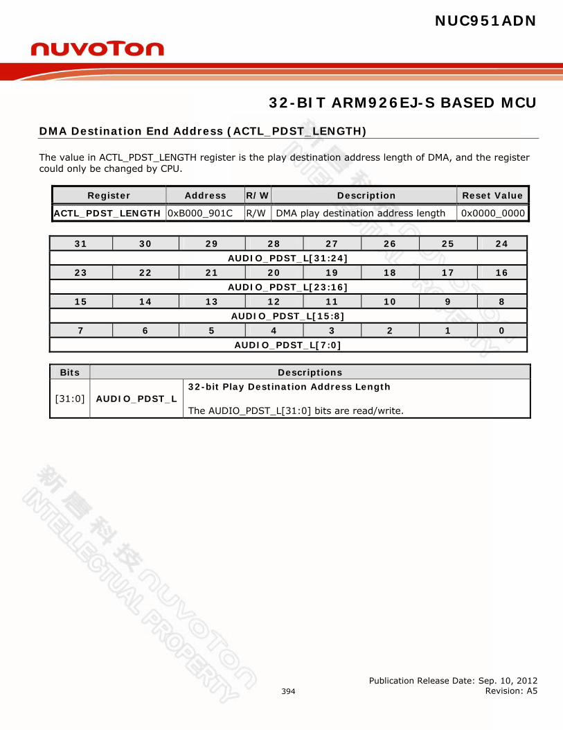
NUC951ADN
32-BIT ARM926EJ-S BASED MCU
Publication Release Date: Sep. 10, 2012 Revision: A5
394
DMA Destination End Address (ACTL_PDST_LENGTH)
The value in ACTL_PDST_LENGTH register is the play destination address length of DMA, and the register could only be changed by CPU.
Register Address R/W Description Reset Value
ACTL_PDST_LENGTH 0xB000_901C R/W DMA play destination address length 0x0000_0000
Bits Descriptions
[31:0] AUDIO_PDST_L 32-bit Play Destination Address Length
The AUDIO_PDST_L[31:0] bits are read/write.
31 30 29 28 27 26 25 24 AUDIO_PDST_L[31:24]
23 22 21 20 19 18 17 16 AUDIO_PDST_L[23:16]
15 14 13 12 11 10 9 8 AUDIO_PDST_L[15:8]
7 6 5 4 3 2 1 0 AUDIO_PDST_L[7:0]
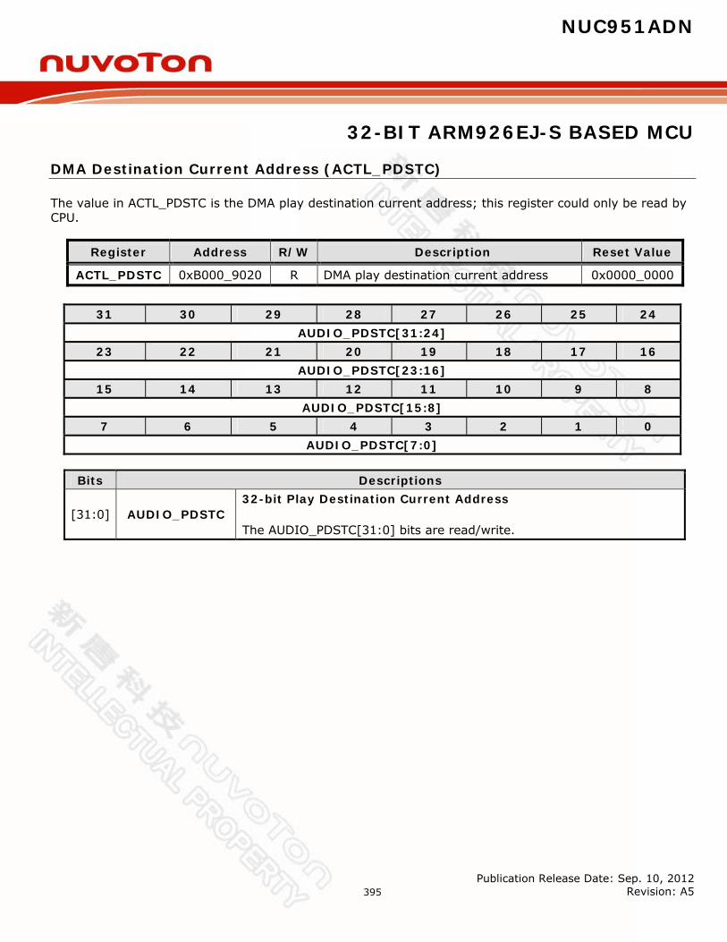
NUC951ADN
32-BIT ARM926EJ-S BASED MCU
Publication Release Date: Sep. 10, 2012 Revision: A5
395
DMA Destination Current Address (ACTL_PDSTC)
The value in ACTL_PDSTC is the DMA play destination current address; this register could only be read by CPU.
Register Address R/W Description Reset Value
ACTL_PDSTC 0xB000_9020 R DMA play destination current address 0x0000_0000
Bits Descriptions
[31:0] AUDIO_PDSTC 32-bit Play Destination Current Address
The AUDIO_PDSTC[31:0] bits are read/write.
31 30 29 28 27 26 25 24 AUDIO_PDSTC[31:24]
23 22 21 20 19 18 17 16 AUDIO_PDSTC[23:16]
15 14 13 12 11 10 9 8 AUDIO_PDSTC[15:8]
7 6 5 4 3 2 1 0 AUDIO_PDSTC[7:0]
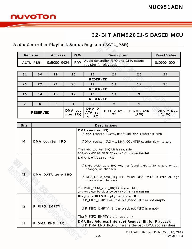
NUC951ADN
32-BIT ARM926EJ-S BASED MCU
Publication Release Date: Sep. 10, 2012 Revision: A5
396
Audio Controller Playback Status Register (ACTL_PSR)
Register Address R/W Description Reset Value
ACTL_PSR 0xB000_9024 R/W Audio controller FIFO and DMA status register for playback 0x0000_0004
Bits Descriptions
[4] DMA_counter_IRQ
DMA counter IRQ If DMA_counter_IRQ=0, not found DMA_counter to zero
If DMA_counter_IRQ =1, DMA_COUNTER counter down to zero
The DMA_counter_IRQ bit is readable , and only can be clear by write “1” to clear this bit
[3] DMA_DATA_zero_IRQ
DMA_DATA zero IRQ
If DMA_DATA_zero_IRQ =0, not found DMA DATA is zero or sign change(two channel)
If DMA_DATA_zero_IRQ =1, found DMA DATA is zero or sign change (two channel)
The DMA_DATA_zero_IRQ bit is readable , and only can be clear by write “1” to clear this bit
[2] P_FIFO_EMPTY
Playback FIFO Empty Indicator Bit If P_FIFO_EMPTY=0, the playback FIFO is not empty
If P_FIFO_EMPTY=1, the playback FIFO is empty
The P_FIFO_EMPTY bit is read only
[1] P_DMA_END_IRQ DMA End Address Interrupt Request Bit for Playback If P_DMA_END_IRQ=0, means playback DMA address does
31 30 29 28 27 26 25 24 RESERVED
23 22 21 20 19 18 17 16 RESERVED
15 14 13 12 11 10 9 8 RESERVED
7 6 5 4 3 2 1 0
RESERVED DMA_counter_IRQ
DMA_DATA_zero_IRQ
P_FIFO_EMPTY
P_DMA_END_IRQ
P_DMA_MIDDLE_IRQ

NUC951ADN
32-BIT ARM926EJ-S BASED MCU
Publication Release Date: Sep. 10, 2012 Revision: A5
397
not reach the end address
If P_DMA_END_IRQ=1, means playback DMA address reach the end address
The P_DMA_END_IRQ bit is readable, and only can be clear by write “1” to this bit
[0] P_DMA_MIDDLE_IRQ
DMA Address Interrupt Request Bit for Playback If P_DMA_MIDDLE_IRQ=0, means playback DMA address
does not reach the middle address
If P_DMA_MIDDLE_IRQ=1, means playback DMA address reach the middle address
The P_DMA_MIDDLE_IRQ bit is readable, and only can be clear by write “1” to this bit
Play (0xB000_9004;bit7,5 )
DMA_DATA_zero_EN (0xB000_9004;bit 3)
DMA_DATA_zero_IRQ (0xB000_9024; bit 3)
1 0 0 play 1 0 0 Play 1 1 0 Play 1 1 1 Play
(output 0,DMA not stop) 0 0 0 stop 0 0 0 Stop 0 1 0 Play 0 1 1 Stop
(DMA stop and output 0 after output data is zero)

NUC951ADN
32-BIT ARM926EJ-S BASED MCU
Publication Release Date: Sep. 10, 2012 Revision: A5
398
IIS Control Register (ACTL_IISCON)
Register Address R/W Description Reset Value
ACTL_IISCON 0xB000_9028 R/W IIS control register 0x0000_0000
Bits Descriptions
[19:16] PRS
IIS Frequency Pre-scalar Selection Bits. (FPLL is the input PLL frequency, MCLK is the output main clock)
If PSR[3:0]=0000, MCLK=FPLL/1
If PSR[3:0]=0001, MCLK=FPLL/2
If PSR[3:0]=0010, MCLK=FPLL/3
If PSR[3:0]=0011, MCLK=FPLL/4
If PSR[3:0]=0100, MCLK=FPLL/5
If PSR[3:0]=0101, MCLK=FPLL/6
If PSR[3:0]=0110, MCLK=FPLL/7
If PSR[3:0]=0111, MCLK=FPLL/8
If PSR[3:0]=1000, reserved
If PSR[3:0]=1001, MCLK=FPLL/10
If PSR[3:0]=1010, reserved
If PSR[3:0]=1011, MCLK=FPLL/12
31 30 29 28 27 26 25 24 RESERVED
23 22 21 20 19 18 17 16 RESERVED PRS[3:0]
15 14 13 12 11 10 9 8 RESERVED
7 6 5 4 3 2 1 0 BCLK_SEL[1:0] FS_SEL MCLK_SEL FORMAT RESERVED
NUC951ADN
32-BIT ARM926EJ-S BASED MCU
Publication Release Date: Sep. 10, 2012 Revision: A5
399
If PSR[3:0]=1100, reserved
If PSR[3:0]=1101, MCLK=FPLL/14
If PSR[3:0]=1110, reserved
If PSR[3:0]=1111, MCLK=FPLL/16
(when the division factor is 3/5/7, the duty cycle of MCLK is not 50%, the high duration is 0.5*FPLL)
The PSR[3:0] bits are read/write
NUC951ADN
32-BIT ARM926EJ-S BASED MCU
Publication Release Date: Sep. 10, 2012 Revision: A5
400
[7:6] BCLK_SEL
IIS Serial Data Clock Frequency Selection Bit If BCLK_SEL[1:0]=00, the frequency of bit clock (BCLK) is MCLK/8,
If BCLK_SEL[1:0]=01, the frequency of bit clock (BCLK) is MCLK/12.
The BCLK_SEL[1:0] bits are read/write
[5] FS_SEL
IIS Sampling Frequency Selection Bit If BCLK_SEL[1:0]=00, and FS_SEL=0, 32fs is selected, the sampling
frequency (LRCLK) = MCLK/(8*32) = MCLK/(256)
If BCLK_SEL[1:0]=00, and FS_SEL=1, 48fs is selected, the sampling frequency (LRCLK) = MCLK/(8*48) = MCLK/(384)
If BCLK_SEL[1:0]=01, this bit is ignored, 32fs is selected, the sampling frequency (LRCLK) = MCLK/(12*32) = MCLK/(384)
(fs is sampling rate)
The FS_SEL bit is read/write Example: MCLK Sample Rate Sample Freq. BCLK_SEL FS_SEL 12.288MHz 32fs 48.0KHz 00 0 16.934MHz 32fs 44.1KHz 01 0
[4] MCLK_SEL
IIS MCLK Output Selection Bit If MCLK_SEL=0, IIS MCLK output will follow the PRS[3:0] setting.
If MCLK_SEL=1, IIS MCLK output will be the same with FPLL.
The MCLK_SEL bit is read/write
[3] FORMAT
IIS Format Selection Bits If FORMAT=0, IIS compatible format is selected
If FORMAT=1, MSB-justified format is selected
The FORMAT bit is read/write
NUC951ADN
32-BIT ARM926EJ-S BASED MCU
Publication Release Date: Sep. 10, 2012 Revision: A5
401
AC-link Control Register (ACTL_ACCON)
Register Address R/W Description Reset Value
ACTL_ACCON 0xB000_902C R/W AC-link control register 0x0000_0000
Bits Descriptions
[5] AC_BCLK_PU_EN
AC_BCLK Pin Pull-high Resister Enable If AC_BCLK_PU_EN=0, the AC_BCLK pin pull-high resister will be
disabled
If AC_BCLK_PU_EN=1, the AC_BCLK pin pull-high resister will be enabled
The AC_BCLK_PU_EN bit is read/write.
[4] AC_R_FINISH
AC-link Read Data Ready Bit. When read data indexed by previous frame is shifted into ACTL_ACIS2, the AC_R_FINISH bit will be set to 1 automatically. After CPU read out the read data, AC_R_FINISH bit will be cleared to 0.
If AC_R_FINISH=0, read data buffer has been read by CPU
If AC_R_FINISH=1, read data buffer is ready for CPU read
The AC_R_FINISH bit is read only
[3] AC_W_FINISH
AC-link Write Frame Finish Bit. When writing data to register ACTL_ACOS0, the AC_W_FINISH bit will be set to 1 automatically. After AC-link interface shift out the register ACTL_ACOS0, the AC_W_FINISH bit will be cleared to 0.
If AC_W_FINISH=0, AC-link control data out buffer has been shifted out to codec by CPU and data out buffer is empty.
If AC_W_FINISH=1, AC-link control data out buffer is ready to be shifted out(After users have wrote data into register
31 30 29 28 27 26 25 24 RESERVED
23 22 21 20 19 18 17 16 RESERVED
15 14 13 12 11 10 9 8 RESERVED
7 6 5 4 3 2 1 0
RESERVED AC_BCLK_PU_EN
AC_R_FINISH
AC_W_FINISH AC_W_RES AC_C_RES RESERVED
NUC951ADN
32-BIT ARM926EJ-S BASED MCU
Publication Release Date: Sep. 10, 2012 Revision: A5
402
ACTL_ACOS0)
The AC_W_FINISH bit is read only

NUC951ADN
32-BIT ARM926EJ-S BASED MCU
Publication Release Date: Sep. 10, 2012 Revision: A5
403
[2] AC_W_RES
AC-link Warm Reset Control Bit When this bit is set to 1, (AC-link begin warn reset procedure, after warn reset procedure finished, this bit will be cleared automatically) the interface signal AC_SYNC is high, when this bit is set to 0, the interface signal AC_SYNC is controlled by AC_BCLK input when this bit is set to 1. Note the AC-link spec. shows it need at least 10 us high duration of AC_SYNC to warn reset AC97.
If AC_W_RES=0, AC_SYNC pin is controlled by AC_BCLK input pin
If AC_W_RES=1, AC_SYNC pin is forced to high
The AC_W_RES bit is read/write
[1] AC_C_RES
AC-link Cold Reset Control Bit When this bit is set to 1, the interface signal AC_RESETB is low, when this bit is set to 0, the signal AC_RESETB is high. Note the AC-link spec. Shows it need at least 10 us low duration of AC_RESETB to cold reset AC97.
If AC_C_RES=0, AC_RESETB pin is set to 1
If AC_C_RES=1, AC_RESETB pin is set to 0
The AC_C_RES bit is read/write

NUC951ADN
32-BIT ARM926EJ-S BASED MCU
Publication Release Date: Sep. 10, 2012 Revision: A5
404
AC-link output slot 0 (ACTL_ACOS0)
The ACTL_ACOS0 register store the slot 0 value to be shift out by AC-link. Note that write data to ACTL_ACOS0 register when AC_W_FINISH bit (ACTL_ACCON[3]) is set is invalid. Therefore, check AC_W_FINISH bit status before write data into ACTL_ACOS0 register.
Register Address R/W Description Reset Value
ACTL_ACOS0 0xB000_9030 R/W AC-link out slot 0 0x0000_0000
Bits Descriptions
[4] VALID_FRAME
Frame Valid Indicated Bits VALID_FRAME=1, any one of slot is valid
VALID_FRAME=0, no any slot is valid
The VALID_FRAME bits are read/write
[3:0] SLOT_VALID[3:0]
Slot Valid Indicated Bits SLOT_VALID[0]= 1/0, indicate Slot 1 valid/invalid
SLOT_VALID[1]= 1/0, indicate Slot 2 valid/invalid
SLOT_VALID[2]= 1/0, indicate Slot 3 valid/invalid
SLOT_VALID[3]= 1/0, indicate Slot 4 valid/invalid
The SLOT_VALID[3:0] bits are read/write
31 30 29 28 27 26 25 24 RESERVED
23 22 21 20 19 18 17 16 RESERVED
15 14 13 12 11 10 9 8 RESERVED
7 6 5 4 3 2 1 0
RESERVED VALID_ FRAME SLOT_VALID[3:0]
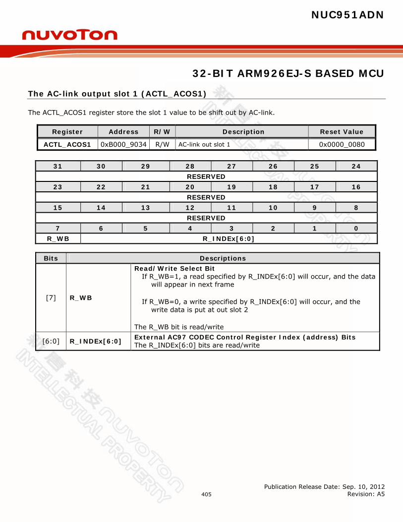
NUC951ADN
32-BIT ARM926EJ-S BASED MCU
Publication Release Date: Sep. 10, 2012 Revision: A5
405
The AC-link output slot 1 (ACTL_ACOS1)
The ACTL_ACOS1 register store the slot 1 value to be shift out by AC-link.
Register Address R/W Description Reset Value
ACTL_ACOS1 0xB000_9034 R/W AC-link out slot 1 0x0000_0080
Bits Descriptions
[7] R_WB
Read/Write Select Bit If R_WB=1, a read specified by R_INDEx[6:0] will occur, and the data
will appear in next frame
If R_WB=0, a write specified by R_INDEx[6:0] will occur, and the write data is put at out slot 2
The R_WB bit is read/write
[6:0] R_INDEx[6:0] External AC97 CODEC Control Register Index (address) Bits The R_INDEx[6:0] bits are read/write
31 30 29 28 27 26 25 24 RESERVED
23 22 21 20 19 18 17 16 RESERVED
15 14 13 12 11 10 9 8 RESERVED
7 6 5 4 3 2 1 0 R_WB R_INDEx[6:0]
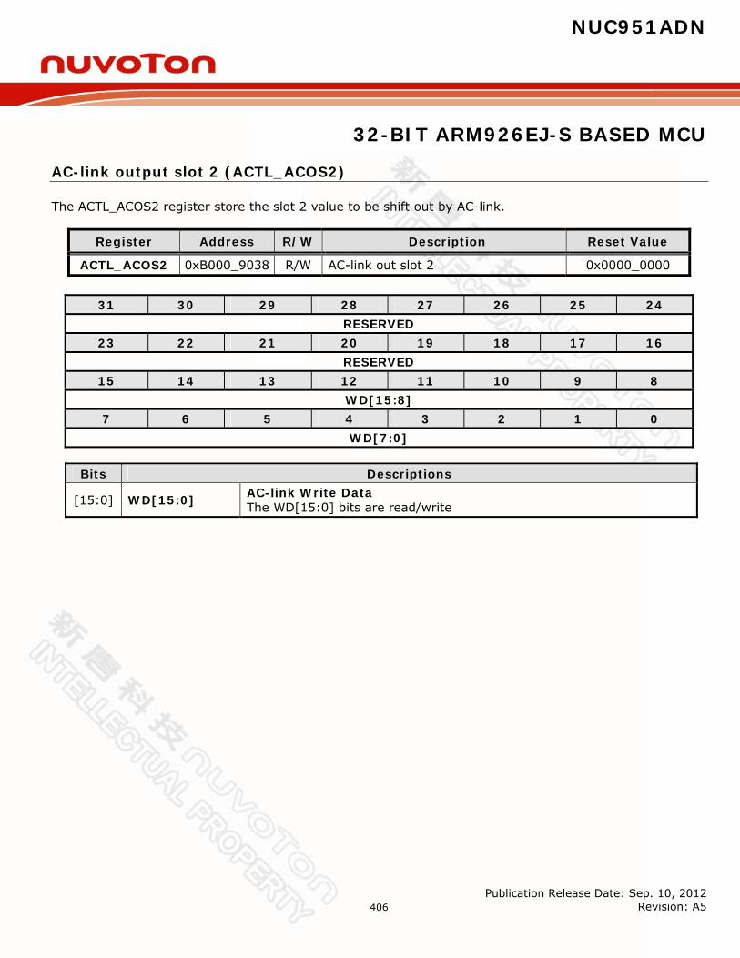
NUC951ADN
32-BIT ARM926EJ-S BASED MCU
Publication Release Date: Sep. 10, 2012 Revision: A5
406
AC-link output slot 2 (ACTL_ACOS2)
The ACTL_ACOS2 register store the slot 2 value to be shift out by AC-link.
Register Address R/W Description Reset Value
ACTL_ACOS2 0xB000_9038 R/W AC-link out slot 2 0x0000_0000
Bits Descriptions
[15:0] WD[15:0] AC-link Write Data The WD[15:0] bits are read/write
31 30 29 28 27 26 25 24 RESERVED
23 22 21 20 19 18 17 16 RESERVED
15 14 13 12 11 10 9 8 WD[15:8]
7 6 5 4 3 2 1 0 WD[7:0]
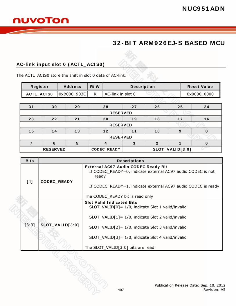
NUC951ADN
32-BIT ARM926EJ-S BASED MCU
Publication Release Date: Sep. 10, 2012 Revision: A5
407
AC-link input slot 0 (ACTL_ACIS0)
The ACTL_ACIS0 store the shift in slot 0 data of AC-link.
Register Address R/W Description Reset Value
ACTL_ACIS0 0xB000_903C R AC-link in slot 0 0x0000_0000
Bits Descriptions
[4] CODEC_READY
External AC97 Audio CODEC Ready Bit If CODEC_READY=0, indicate external AC97 audio CODEC is not
ready
If CODEC_READY=1, indicate external AC97 audio CODEC is ready
The CODEC_READY bit is read only
[3:0] SLOT_VALID[3:0]
Slot Valid Indicated Bits SLOT_VALID[0]= 1/0, indicate Slot 1 valid/invalid
SLOT_VALID[1]= 1/0, indicate Slot 2 valid/invalid
SLOT_VALID[2]= 1/0, indicate Slot 3 valid/invalid
SLOT_VALID[3]= 1/0, indicate Slot 4 valid/invalid
The SLOT_VALID[3:0] bits are read
31 30 29 28 27 26 25 24 RESERVED
23 22 21 20 19 18 17 16 RESERVED
15 14 13 12 11 10 9 8 RESERVED
7 6 5 4 3 2 1 0 RESERVED CODEC_READY SLOT_VALID[3:0]

NUC951ADN
32-BIT ARM926EJ-S BASED MCU
Publication Release Date: Sep. 10, 2012 Revision: A5
408
AC-link input slot 1 (ACTL_ACIS1)
Register Address R/W Description Reset Value
ACTL_ACIS1 0xB000_9040 R AC-link in slot 1 0x0000_0000 The ACTL_ACIS1 stores the shift in slot 1 data of AC-link.
Bits Descriptions
[8:2] R_INDEx[6:0]
Register Index. The R_INDEx[6:0] echo the register index (address) when a register read has been requested in the previous frame. The R_INDEx[6:0] bits are read only
[1:0] SLOT_REQ[1:0]
Slot Request. The bits indicate if the external codec need new PCM data that will transfer in next frame.
Any bit in SLOT_REQ[1:0] is set to 1, indicate external codec does not need a new sample in the corresponding slot[3:4] of the next frame
Any SLOT_REQ[1:0] is clear to 0, indicate external codec need a new sample in the corresponding slot[3:4] of the next frame
The SLOT_REQ[1:0] bits are read only
31 30 29 28 27 26 25 24 RESERVED
23 22 21 20 19 18 17 16 RESERVED
15 14 13 12 11 10 9 8 RESERVED R_INDEx[6]
7 6 5 4 3 2 1 0 R_INDEx[5:0] SLOT_REQ[1:0]
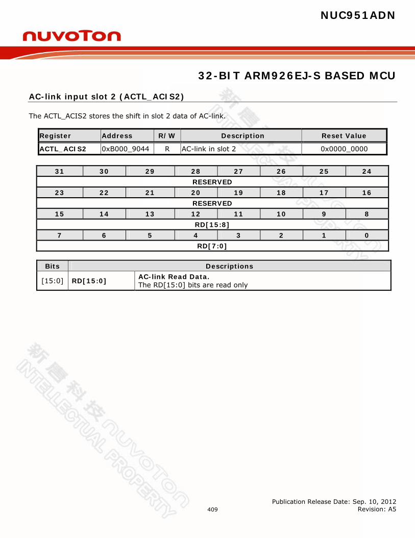
NUC951ADN
32-BIT ARM926EJ-S BASED MCU
Publication Release Date: Sep. 10, 2012 Revision: A5
409
AC-link input slot 2 (ACTL_ACIS2)
The ACTL_ACIS2 stores the shift in slot 2 data of AC-link.
Register Address R/W Description Reset Value
ACTL_ACIS2 0xB000_9044 R AC-link in slot 2 0x0000_0000
Bits Descriptions
[15:0] RD[15:0] AC-link Read Data. The RD[15:0] bits are read only
31 30 29 28 27 26 25 24 RESERVED
23 22 21 20 19 18 17 16 RESERVED
15 14 13 12 11 10 9 8 RD[15:8]
7 6 5 4 3 2 1 0 RD[7:0]
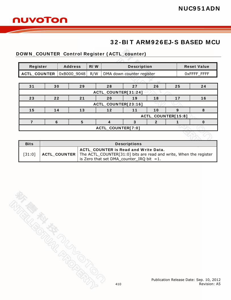
NUC951ADN
32-BIT ARM926EJ-S BASED MCU
Publication Release Date: Sep. 10, 2012 Revision: A5
410
DOWN_COUNTER Control Register (ACTL_counter)
Register Address R/W Description Reset Value
ACTL_COUNTER 0xB000_9048 R/W DMA down counter register 0xFFFF_FFFF
Bits Descriptions
[31:0] ACTL_COUNTER ACTL_COUNTER is Read and Write Data. The ACTL_COUNTER[31:0] bits are read and write, When the register is Zero that set DMA_counter_IRQ bit =1.
31 30 29 28 27 26 25 24 ACTL_COUNTER[31:24]
23 22 21 20 19 18 17 16 ACTL_COUNTER[23:16]
15 14 13 12 11 10 9 8 ACTL_COUNTER[15:8]
7 6 5 4 3 2 1 0 ACTL_COUNTER[7:0]
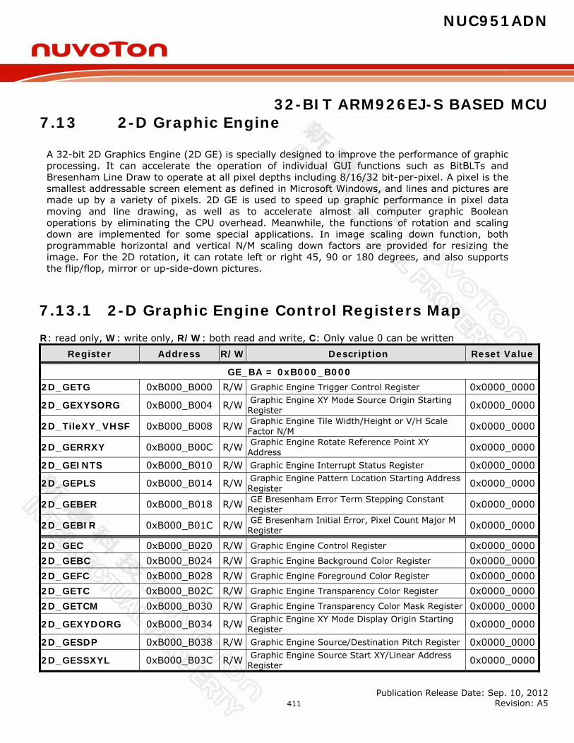
NUC951ADN
32-BIT ARM926EJ-S BASED MCU
Publication Release Date: Sep. 10, 2012 Revision: A5
411
7.13 2-D Graphic Engine
A 32-bit 2D Graphics Engine (2D GE) is specially designed to improve the performance of graphic processing. It can accelerate the operation of individual GUI functions such as BitBLTs and Bresenham Line Draw to operate at all pixel depths including 8/16/32 bit-per-pixel. A pixel is the smallest addressable screen element as defined in Microsoft Windows, and lines and pictures are made up by a variety of pixels. 2D GE is used to speed up graphic performance in pixel data moving and line drawing, as well as to accelerate almost all computer graphic Boolean operations by eliminating the CPU overhead. Meanwhile, the functions of rotation and scaling down are implemented for some special applications. In image scaling down function, both programmable horizontal and vertical N/M scaling down factors are provided for resizing the image. For the 2D rotation, it can rotate left or right 45, 90 or 180 degrees, and also supports the flip/flop, mirror or up-side-down pictures.
7.13.1 2-D Graphic Engine Control Registers Map R: read only, W: write only, R/W: both read and write, C: Only value 0 can be written
Register Address R/W Description Reset Value
GE_BA = 0xB000_B000 2D_GETG 0xB000_B000 R/W Graphic Engine Trigger Control Register 0x0000_0000
2D_GEXYSORG 0xB000_B004 R/W Graphic Engine XY Mode Source Origin Starting Register 0x0000_0000
2D_TileXY_VHSF 0xB000_B008 R/W Graphic Engine Tile Width/Height or V/H Scale Factor N/M 0x0000_0000
2D_GERRXY 0xB000_B00C R/W Graphic Engine Rotate Reference Point XY Address 0x0000_0000
2D_GEINTS 0xB000_B010 R/W Graphic Engine Interrupt Status Register 0x0000_0000
2D_GEPLS 0xB000_B014 R/W Graphic Engine Pattern Location Starting Address Register 0x0000_0000
2D_GEBER 0xB000_B018 R/W GE Bresenham Error Term Stepping Constant Register 0x0000_0000
2D_GEBIR 0xB000_B01C R/W GE Bresenham Initial Error, Pixel Count Major M Register 0x0000_0000
2D_GEC 0xB000_B020 R/W Graphic Engine Control Register 0x0000_0000 2D_GEBC 0xB000_B024 R/W Graphic Engine Background Color Register 0x0000_0000 2D_GEFC 0xB000_B028 R/W Graphic Engine Foreground Color Register 0x0000_0000 2D_GETC 0xB000_B02C R/W Graphic Engine Transparency Color Register 0x0000_0000 2D_GETCM 0xB000_B030 R/W Graphic Engine Transparency Color Mask Register 0x0000_0000
2D_GEXYDORG 0xB000_B034 R/W Graphic Engine XY Mode Display Origin Starting Register 0x0000_0000
2D_GESDP 0xB000_B038 R/W Graphic Engine Source/Destination Pitch Register 0x0000_0000
2D_GESSXYL 0xB000_B03C R/W Graphic Engine Source Start XY/Linear Address Register 0x0000_0000
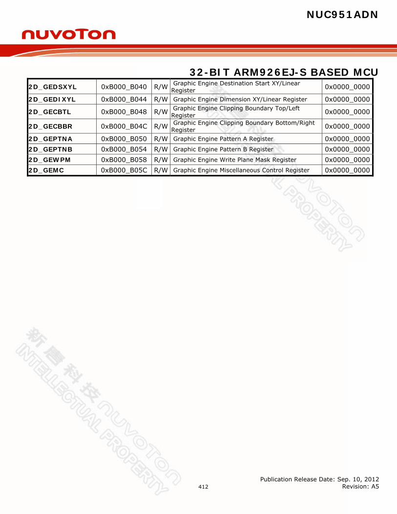
NUC951ADN
32-BIT ARM926EJ-S BASED MCU
Publication Release Date: Sep. 10, 2012 Revision: A5
412
2D_GEDSXYL 0xB000_B040 R/W Graphic Engine Destination Start XY/Linear Register 0x0000_0000
2D_GEDIXYL 0xB000_B044 R/W Graphic Engine Dimension XY/Linear Register 0x0000_0000
2D_GECBTL 0xB000_B048 R/W Graphic Engine Clipping Boundary Top/Left Register 0x0000_0000
2D_GECBBR 0xB000_B04C R/W Graphic Engine Clipping Boundary Bottom/Right Register 0x0000_0000
2D_GEPTNA 0xB000_B050 R/W Graphic Engine Pattern A Register 0x0000_0000 2D_GEPTNB 0xB000_B054 R/W Graphic Engine Pattern B Register 0x0000_0000 2D_GEWPM 0xB000_B058 R/W Graphic Engine Write Plane Mask Register 0x0000_0000 2D_GEMC 0xB000_B05C R/W Graphic Engine Miscellaneous Control Register 0x0000_0000
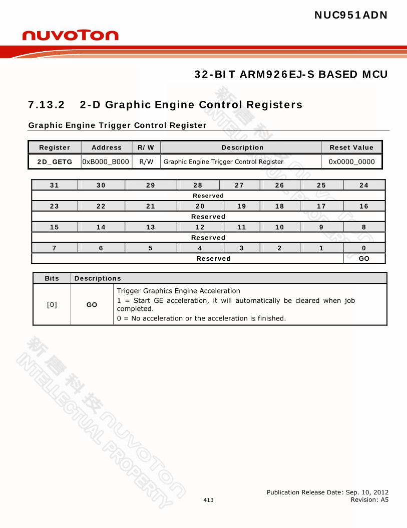
NUC951ADN
32-BIT ARM926EJ-S BASED MCU
Publication Release Date: Sep. 10, 2012 Revision: A5
413
7.13.2 2-D Graphic Engine Control Registers
Graphic Engine Trigger Control Register
Register Address R/W Description Reset Value
2D_GETG 0xB000_B000 R/W Graphic Engine Trigger Control Register 0x0000_0000
Bits Descriptions
[0] GO
Trigger Graphics Engine Acceleration 1 = Start GE acceleration, it will automatically be cleared when job completed. 0 = No acceleration or the acceleration is finished.
31 30 29 28 27 26 25 24 Reserved
23 22 21 20 19 18 17 16 Reserved
15 14 13 12 11 10 9 8 Reserved
7 6 5 4 3 2 1 0 Reserved GO
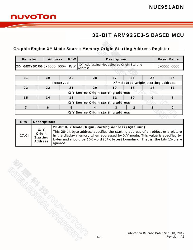
NUC951ADN
32-BIT ARM926EJ-S BASED MCU
Publication Release Date: Sep. 10, 2012 Revision: A5
414
Graphic Engine XY Mode Source Memory Origin Starting Address Register
Register Address R/W Description Reset Value
2D_GEXYSORG 0xB000_B004 R/W X/Y Addressing Mode Source Origin Starting Address 0x0000_0000
Bits Descriptions
[27:0]
X/Y Origin
Starting Address
28-bit X/Y Mode Origin Starting Address (byte unit) This 28-bit byte address specifies the starting address of an object or a picture in the display memory when addressed by X/Y mode. This value is specified by bytes and should be 16K word (64K bytes) boundary. That is, the bits 15-0 are ignored.
31 30 29 28 27 26 25 24 Reserved X/Y Source Origin starting address
23 22 21 20 19 18 17 16 X/Y Source Origin starting address
15 14 13 12 11 10 9 8 X/Y Source Origin starting address
7 6 5 4 3 2 1 0 X/Y Source Origin starting address
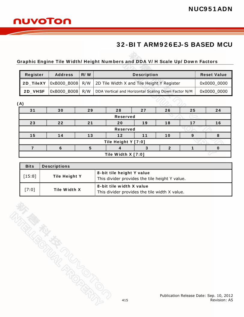
NUC951ADN
32-BIT ARM926EJ-S BASED MCU
Publication Release Date: Sep. 10, 2012 Revision: A5
415
Graphic Engine Tile Width/Height Numbers and DDA V/H Scale Up/Down Factors
Register Address R/W Description Reset Value
2D_TileXY 0xB000_B008 R/W 2D Tile Width X and Tile Height Y Register 0x0000_0000
2D_VHSF 0xB000_B008 R/W DDA Vertical and Horizontal Scaling Down Factor N/M 0x0000_0000
(A)
Bits Descriptions
[15:8] Tile Height Y 8-bit tile height Y value This divider provides the tile height Y value.
[7:0] Tile Width X 8-bit tile width X value This divider provides the tile width X value.
31 30 29 28 27 26 25 24 Reserved
23 22 21 20 19 18 17 16 Reserved
15 14 13 12 11 10 9 8 Tile Height Y [7:0]
7 6 5 4 3 2 1 0 Tile Width X [7:0]

NUC951ADN
32-BIT ARM926EJ-S BASED MCU
Publication Release Date: Sep. 10, 2012 Revision: A5
416
(B)
Bits Descriptions
[31:24] VSF_N
8-bit Vertical N Scaling Factor An 8-bit value specifies the numerator part (N) of the vertical scaling factor in graphic engine. The output image height will be equal to the input image height x N / M. The value of N must be equal or less than M.
[23:16] VSF_M
8-bit Vertical M Scaling Factor An 8-bit value specifies the denominator part (M) of the vertical scaling factor in graphic engine. The output image height will be equal to the input image height x N / M. The value of N must be equal or less than M.
[15:8] HSF_N
8-bit Horizontal N Scaling Factor An 8-bit value specifies the numerator part (N) of the horizontal scaling factor in graphic engine. The output image width will be equal to the input image width x N / M. The value of N must be equal or less than M.
[7:0] HSF_M
8-bit Horizontal M Scaling Factor An 8-bit value specifies the denominator part (M) of the horizontal scaling factor in graphic engine. The output image width will be equal to the input image width x N / M. The value of N must be equal or less than M.
31 30 29 28 27 26 25 24 VSF_N [7:0]
23 22 21 20 19 18 17 16 VSF_M [7:0]
15 14 13 12 11 10 9 8 HSF_N [7:0]
7 6 5 4 3 2 1 0 HSF_M [7:0]
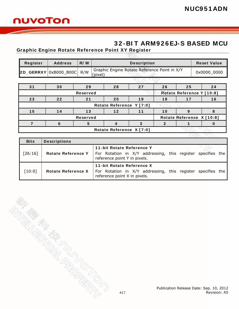
NUC951ADN
32-BIT ARM926EJ-S BASED MCU
Publication Release Date: Sep. 10, 2012 Revision: A5
417
Graphic Engine Rotate Reference Point XY Register
Register Address R/W Description Reset Value
2D_GERRXY 0xB000_B00C R/W Graphic Engine Rotate Reference Point in X/Y (pixel) 0x0000_0000
Bits Descriptions
[26:16] Rotate Reference Y 11-bit Rotate Reference Y For Rotation in X/Y addressing, this register specifies the reference point Y in pixels.
[10:0] Rotate Reference X 11-bit Rotate Reference X For Rotation in X/Y addressing, this register specifies the reference point X in pixels.
31 30 29 28 27 26 25 24 Reserved Rotate Reference Y [10:8]
23 22 21 20 19 18 17 16 Rotate Reference Y [7:0]
15 14 13 12 11 10 9 8 Reserved Rotate Reference X [10:8]
7 6 5 4 3 2 1 0 Rotate Reference X [7:0]
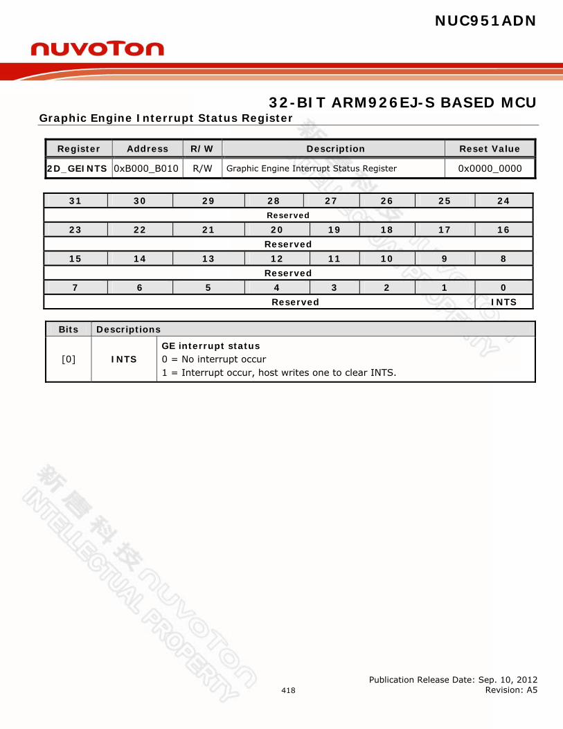
NUC951ADN
32-BIT ARM926EJ-S BASED MCU
Publication Release Date: Sep. 10, 2012 Revision: A5
418
Graphic Engine Interrupt Status Register
Register Address R/W Description Reset Value
2D_GEINTS 0xB000_B010 R/W Graphic Engine Interrupt Status Register 0x0000_0000
Bits Descriptions
[0] INTS GE interrupt status 0 = No interrupt occur 1 = Interrupt occur, host writes one to clear INTS.
31 30 29 28 27 26 25 24 Reserved
23 22 21 20 19 18 17 16 Reserved
15 14 13 12 11 10 9 8 Reserved
7 6 5 4 3 2 1 0 Reserved INTS
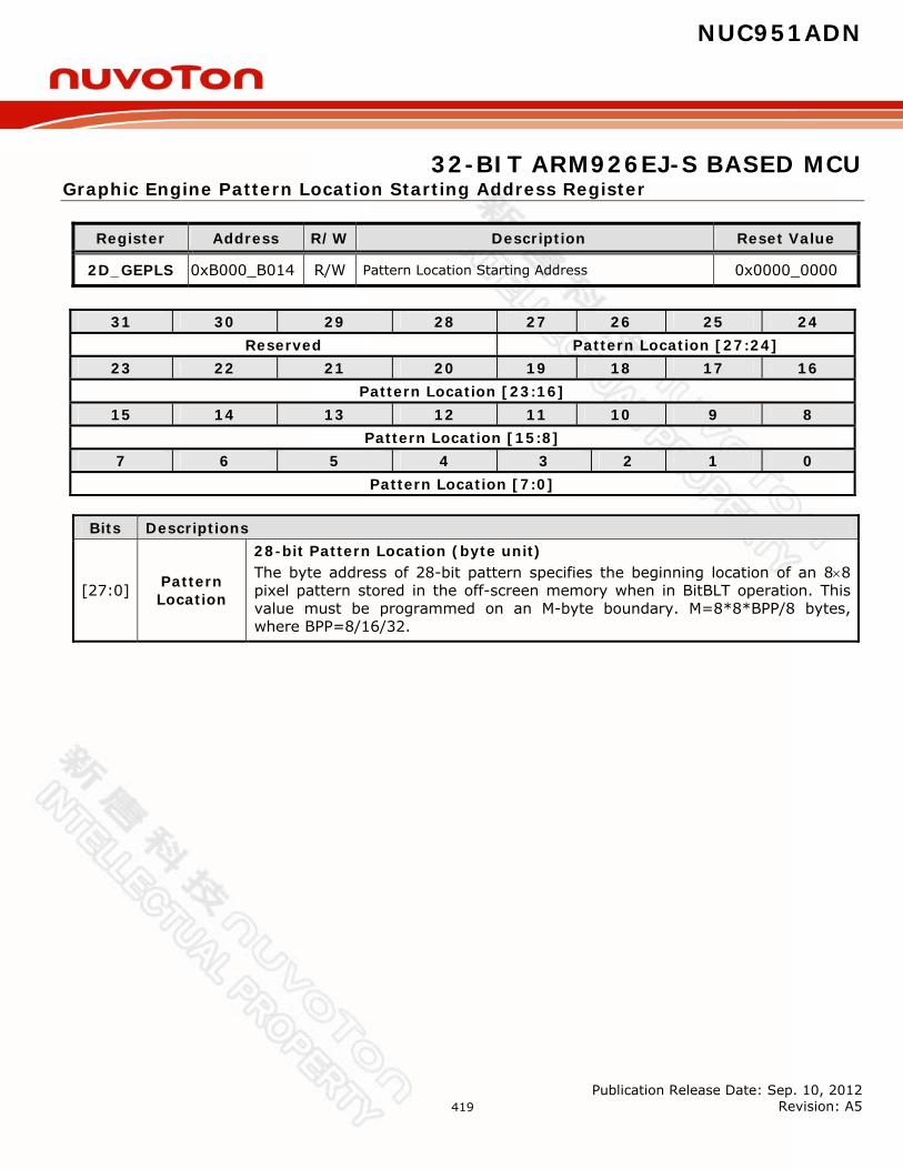
NUC951ADN
32-BIT ARM926EJ-S BASED MCU
Publication Release Date: Sep. 10, 2012 Revision: A5
419
Graphic Engine Pattern Location Starting Address Register
Register Address R/W Description Reset Value
2D_GEPLS 0xB000_B014 R/W Pattern Location Starting Address 0x0000_0000
Bits Descriptions
[27:0] Pattern Location
28-bit Pattern Location (byte unit) The byte address of 28-bit pattern specifies the beginning location of an 88 pixel pattern stored in the off-screen memory when in BitBLT operation. This value must be programmed on an M-byte boundary. M=8*8*BPP/8 bytes, where BPP=8/16/32.
31 30 29 28 27 26 25 24 Reserved Pattern Location [27:24]
23 22 21 20 19 18 17 16 Pattern Location [23:16]
15 14 13 12 11 10 9 8 Pattern Location [15:8]
7 6 5 4 3 2 1 0 Pattern Location [7:0]
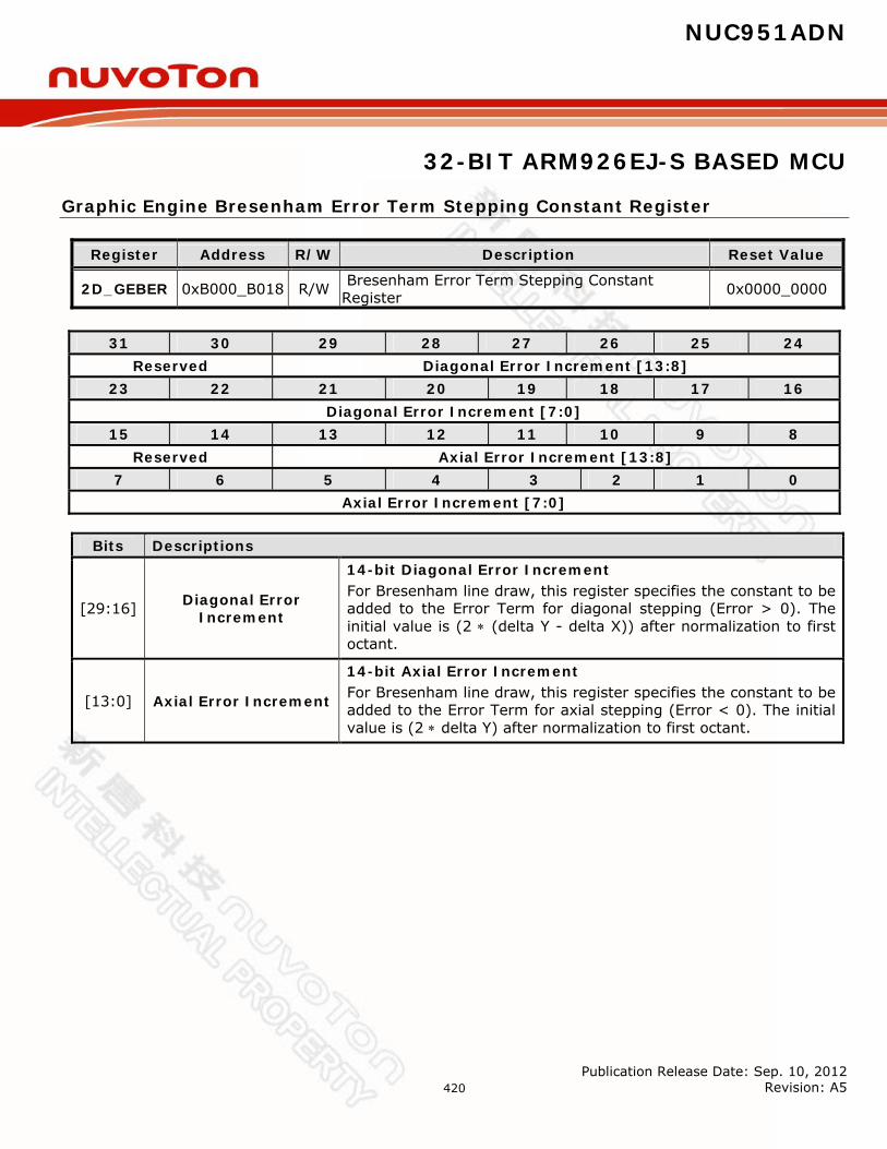
NUC951ADN
32-BIT ARM926EJ-S BASED MCU
Publication Release Date: Sep. 10, 2012 Revision: A5
420
Graphic Engine Bresenham Error Term Stepping Constant Register
Register Address R/W Description Reset Value
2D_GEBER 0xB000_B018 R/W Bresenham Error Term Stepping Constant Register 0x0000_0000
Bits Descriptions
[29:16] Diagonal Error Increment
14-bit Diagonal Error Increment For Bresenham line draw, this register specifies the constant to be added to the Error Term for diagonal stepping (Error > 0). The initial value is (2 (delta Y - delta X)) after normalization to first octant.
[13:0] Axial Error Increment
14-bit Axial Error Increment For Bresenham line draw, this register specifies the constant to be added to the Error Term for axial stepping (Error < 0). The initial value is (2 delta Y) after normalization to first octant.
31 30 29 28 27 26 25 24 Reserved Diagonal Error Increment [13:8]
23 22 21 20 19 18 17 16 Diagonal Error Increment [7:0]
15 14 13 12 11 10 9 8 Reserved Axial Error Increment [13:8]
7 6 5 4 3 2 1 0 Axial Error Increment [7:0]
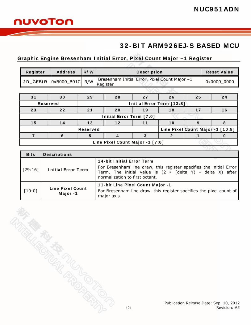
NUC951ADN
32-BIT ARM926EJ-S BASED MCU
Publication Release Date: Sep. 10, 2012 Revision: A5
421
Graphic Engine Bresenham Initial Error, Pixel Count Major –1 Register
Register Address R/W Description Reset Value
2D_GEBIR 0xB000_B01C R/W Bresenham Initial Error, Pixel Count Major –1 Register 0x0000_0000
Bits Descriptions
[29:16] Initial Error Term
14-bit Initial Error Term For Bresenham line draw, this register specifies the initial Error Term. The initial value is (2 (delta Y) - delta X) after normalization to first octant.
[10:0] Line Pixel Count Major -1
11-bit Line Pixel Count Major -1 For Bresenham line draw, this register specifies the pixel count of major axis
31 30 29 28 27 26 25 24 Reserved Initial Error Term [13:8]
23 22 21 20 19 18 17 16 Initial Error Term [7:0]
15 14 13 12 11 10 9 8 Reserved Line Pixel Count Major -1 [10:8]
7 6 5 4 3 2 1 0 Line Pixel Count Major -1 [7:0]
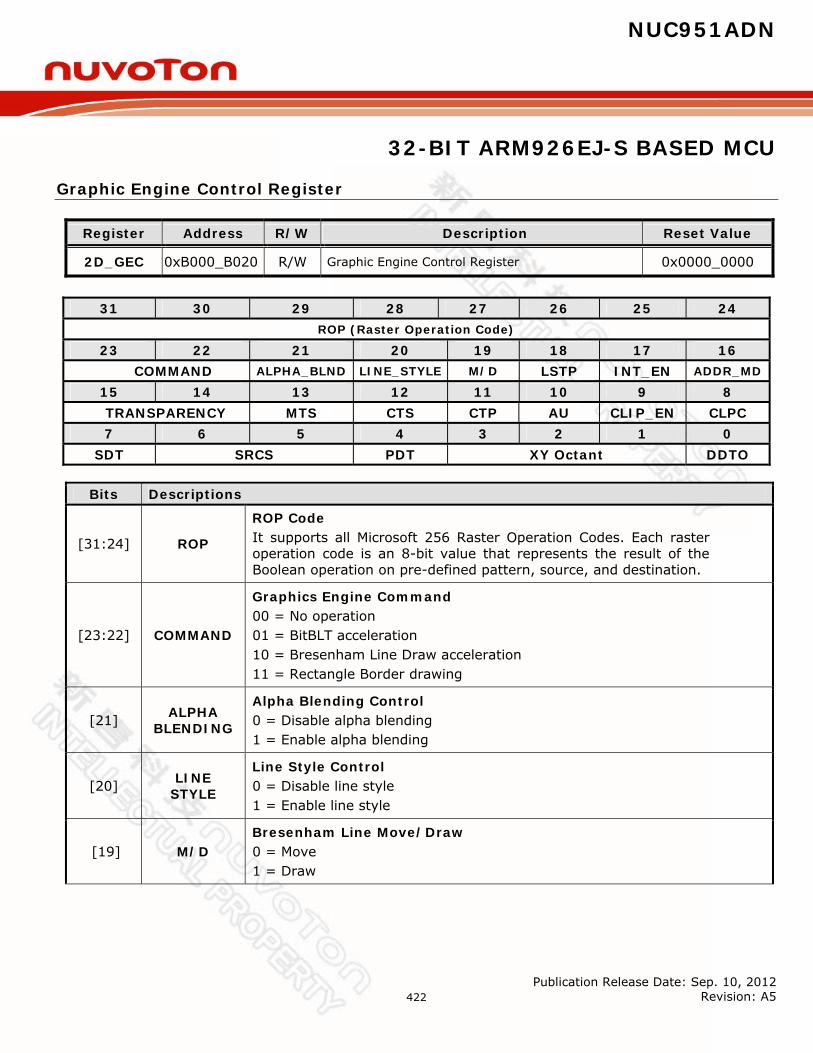
NUC951ADN
32-BIT ARM926EJ-S BASED MCU
Publication Release Date: Sep. 10, 2012 Revision: A5
422
Graphic Engine Control Register
Register Address R/W Description Reset Value
2D_GEC 0xB000_B020 R/W Graphic Engine Control Register 0x0000_0000
Bits Descriptions
[31:24] ROP
ROP Code It supports all Microsoft 256 Raster Operation Codes. Each raster operation code is an 8-bit value that represents the result of the Boolean operation on pre-defined pattern, source, and destination.
[23:22] COMMAND
Graphics Engine Command 00 = No operation 01 = BitBLT acceleration 10 = Bresenham Line Draw acceleration 11 = Rectangle Border drawing
[21] ALPHA BLENDING
Alpha Blending Control 0 = Disable alpha blending 1 = Enable alpha blending
[20] LINE STYLE
Line Style Control 0 = Disable line style 1 = Enable line style
[19] M/D Bresenham Line Move/Draw 0 = Move 1 = Draw
31 30 29 28 27 26 25 24 ROP (Raster Operation Code)
23 22 21 20 19 18 17 16 COMMAND ALPHA_BLND LINE_STYLE M/D LSTP INT_EN ADDR_MD
15 14 13 12 11 10 9 8 TRANSPARENCY MTS CTS CTP AU CLIP_EN CLPC 7 6 5 4 3 2 1 0
SDT SRCS PDT XY Octant DDTO
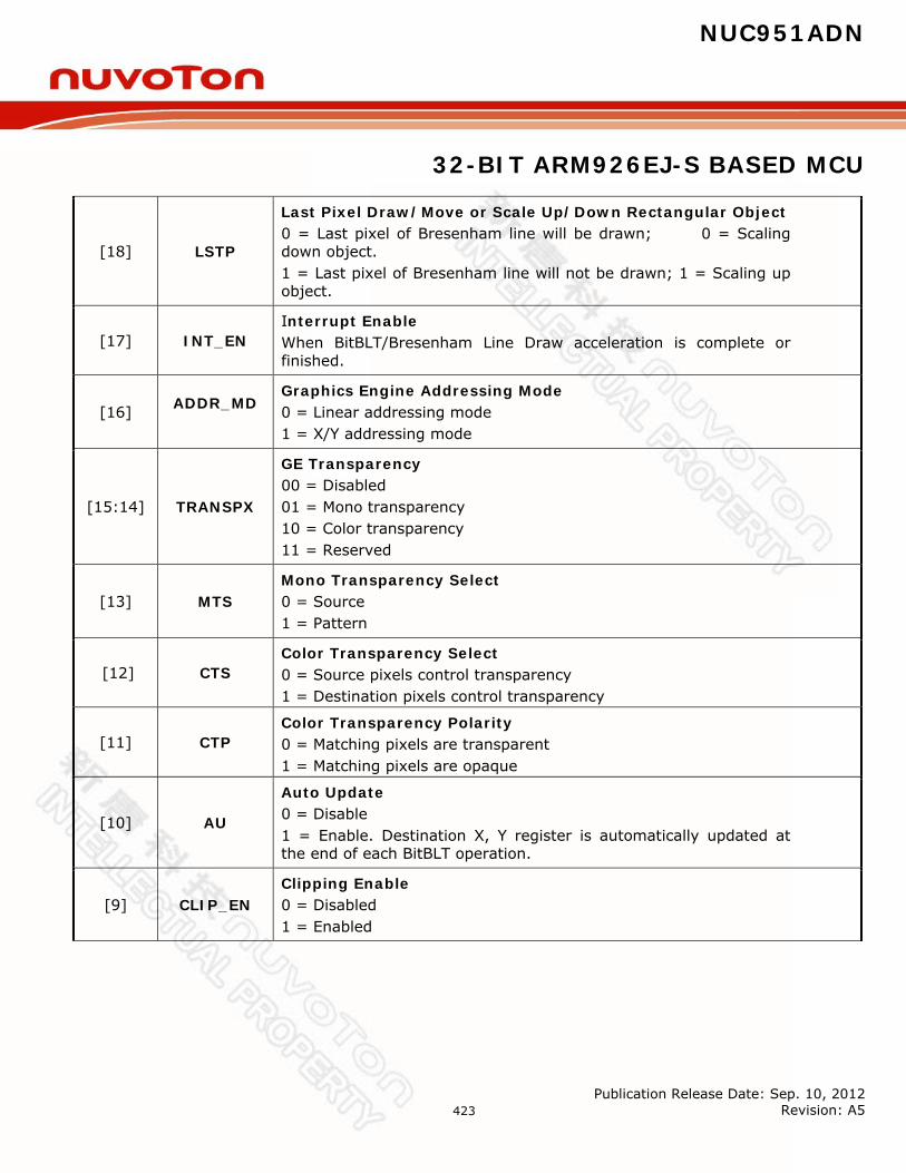
NUC951ADN
32-BIT ARM926EJ-S BASED MCU
Publication Release Date: Sep. 10, 2012 Revision: A5
423
[18] LSTP
Last Pixel Draw/Move or Scale Up/Down Rectangular Object 0 = Last pixel of Bresenham line will be drawn; 0 = Scaling down object. 1 = Last pixel of Bresenham line will not be drawn; 1 = Scaling up object.
[17] INT_EN Interrupt Enable When BitBLT/Bresenham Line Draw acceleration is complete or finished.
[16] ADDR_MD
Graphics Engine Addressing Mode 0 = Linear addressing mode 1 = X/Y addressing mode
[15:14] TRANSPX
GE Transparency 00 = Disabled 01 = Mono transparency 10 = Color transparency 11 = Reserved
[13] MTS Mono Transparency Select 0 = Source 1 = Pattern
[12] CTS Color Transparency Select 0 = Source pixels control transparency 1 = Destination pixels control transparency
[11] CTP Color Transparency Polarity 0 = Matching pixels are transparent 1 = Matching pixels are opaque
[10] AU
Auto Update 0 = Disable 1 = Enable. Destination X, Y register is automatically updated at the end of each BitBLT operation.
[9] CLIP_EN Clipping Enable 0 = Disabled 1 = Enabled
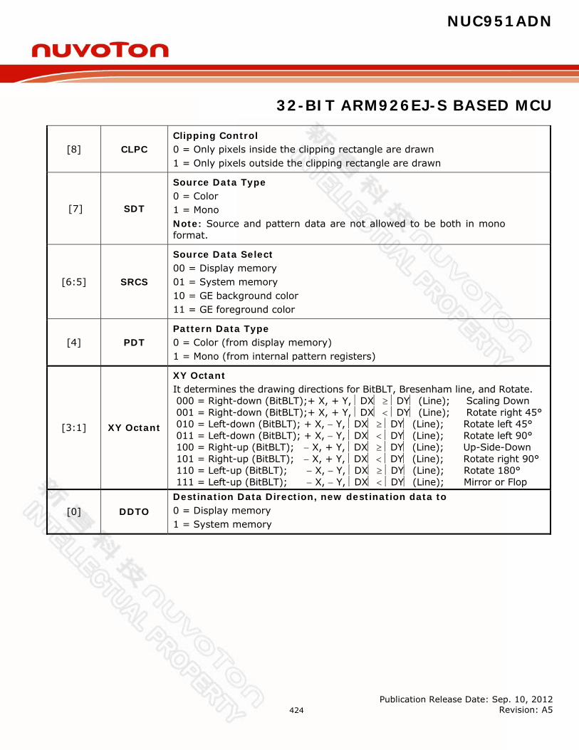
NUC951ADN
32-BIT ARM926EJ-S BASED MCU
Publication Release Date: Sep. 10, 2012 Revision: A5
424
[8] CLPC Clipping Control 0 = Only pixels inside the clipping rectangle are drawn 1 = Only pixels outside the clipping rectangle are drawn
[7] SDT
Source Data Type 0 = Color 1 = Mono Note: Source and pattern data are not allowed to be both in mono format.
[6:5] SRCS
Source Data Select 00 = Display memory 01 = System memory 10 = GE background color 11 = GE foreground color
[4] PDT Pattern Data Type 0 = Color (from display memory) 1 = Mono (from internal pattern registers)
[3:1] XY Octant
XY Octant It determines the drawing directions for BitBLT, Bresenham line, and Rotate. 000 = Right-down (BitBLT);+ X, + Y, DX DY (Line); Scaling Down 001 = Right-down (BitBLT);+ X, + Y, DX DY (Line); Rotate right 45° 010 = Left-down (BitBLT); + X, Y, DX DY (Line); Rotate left 45° 011 = Left-down (BitBLT); + X, Y, DX DY (Line); Rotate left 90° 100 = Right-up (BitBLT); X, + Y, DX DY (Line); Up-Side-Down 101 = Right-up (BitBLT); X, + Y, DX DY (Line); Rotate right 90° 110 = Left-up (BitBLT); X, Y, DX DY (Line); Rotate 180° 111 = Left-up (BitBLT); X, Y, DX DY (Line); Mirror or Flop
[0] DDTO Destination Data Direction, new destination data to 0 = Display memory 1 = System memory

NUC951ADN
32-BIT ARM926EJ-S BASED MCU
Publication Release Date: Sep. 10, 2012 Revision: A5
425
Graphic Engine Background Color Register
Register Address R/W Description Reset Value
2D_GEBC 0xB000_B024 R/W Graphic Engine Background Color 0x0000_0000
= Bits Descriptions
[23:0] Background Color
24-bit Background Color These bits specify the background color for Graphics Engine. Only the corresponding number of bits-per-pixel in the display mode is required in the register. In RGB 8:8:8 color mode, bits 23-16 have the red value, bits 15-8 have the green value, and bits 7-0 have the blue value.
31 30 29 28 27 26 25 24 Reserved
23 22 21 20 19 18 17 16 Background Color [23:16]
15 14 13 12 11 10 9 8 Background Color [15:8]
7 6 5 4 3 2 1 0 Background Color [7:0]
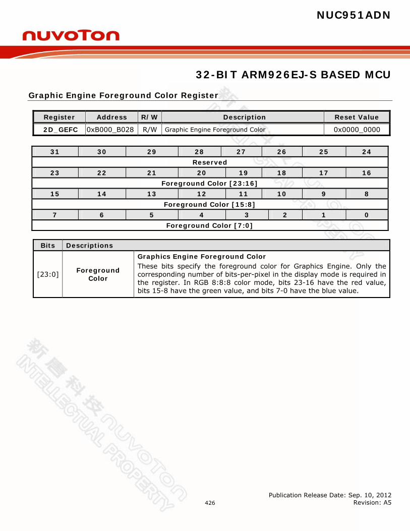
NUC951ADN
32-BIT ARM926EJ-S BASED MCU
Publication Release Date: Sep. 10, 2012 Revision: A5
426
Graphic Engine Foreground Color Register
Register Address R/W Description Reset Value
2D_GEFC 0xB000_B028 R/W Graphic Engine Foreground Color 0x0000_0000
Bits Descriptions
[23:0] Foreground Color
Graphics Engine Foreground Color These bits specify the foreground color for Graphics Engine. Only the corresponding number of bits-per-pixel in the display mode is required in the register. In RGB 8:8:8 color mode, bits 23-16 have the red value, bits 15-8 have the green value, and bits 7-0 have the blue value.
31 30 29 28 27 26 25 24 Reserved
23 22 21 20 19 18 17 16 Foreground Color [23:16]
15 14 13 12 11 10 9 8 Foreground Color [15:8]
7 6 5 4 3 2 1 0 Foreground Color [7:0]
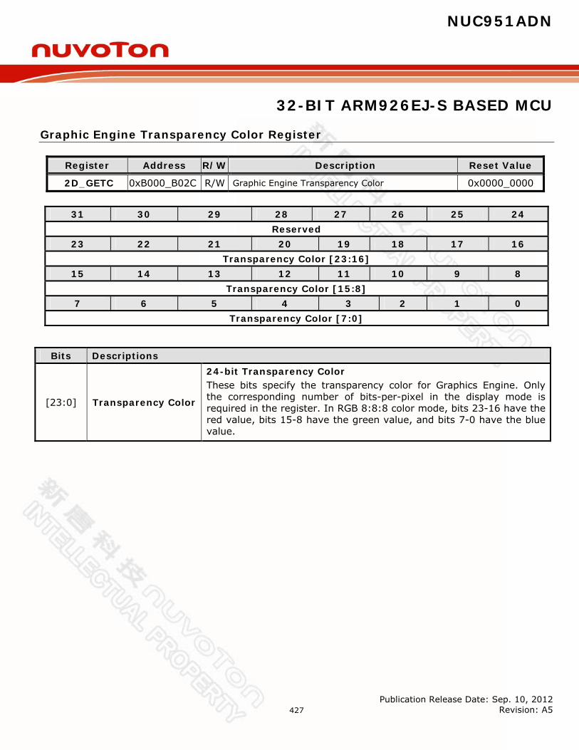
NUC951ADN
32-BIT ARM926EJ-S BASED MCU
Publication Release Date: Sep. 10, 2012 Revision: A5
427
Graphic Engine Transparency Color Register
Register Address R/W Description Reset Value
2D_GETC 0xB000_B02C R/W Graphic Engine Transparency Color 0x0000_0000
Bits Descriptions
[23:0] Transparency Color
24-bit Transparency Color These bits specify the transparency color for Graphics Engine. Only the corresponding number of bits-per-pixel in the display mode is required in the register. In RGB 8:8:8 color mode, bits 23-16 have the red value, bits 15-8 have the green value, and bits 7-0 have the blue value.
31 30 29 28 27 26 25 24 Reserved
23 22 21 20 19 18 17 16 Transparency Color [23:16]
15 14 13 12 11 10 9 8 Transparency Color [15:8]
7 6 5 4 3 2 1 0 Transparency Color [7:0]

NUC951ADN
32-BIT ARM926EJ-S BASED MCU
Publication Release Date: Sep. 10, 2012 Revision: A5
428
Graphic Engine Transparency Color Mask Register
Register Address R/W Description Reset Value
2D_GETCM 0xB000_B030 R/W Graphic Engine Transparency Color Mask 0x0000_0000
Bits Descriptions
[23:0] Transparency Color Mask
24-bit Transparency Color Mask These bits specify a mask for use in comparison against the transparency color. Only the corresponding number of bits-per-pixel in the display mode is required in the register.
31 30 29 28 27 26 25 24 Reserved
23 22 21 20 19 18 17 16 Transparency Color Mask [23:16]
15 14 13 12 11 10 9 8 Transparency Color Mask [15:8]
7 6 5 4 3 2 1 0 Transparency Color Mask [7:0]
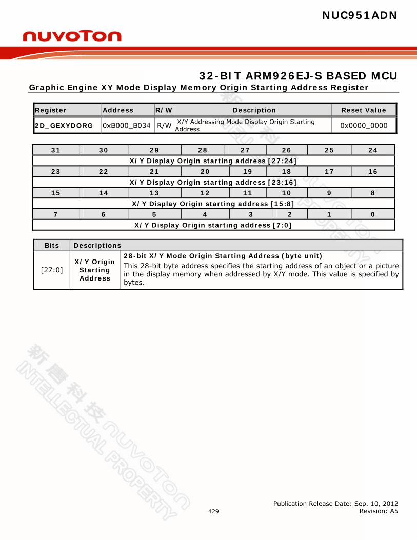
NUC951ADN
32-BIT ARM926EJ-S BASED MCU
Publication Release Date: Sep. 10, 2012 Revision: A5
429
Graphic Engine XY Mode Display Memory Origin Starting Address Register
Register Address R/W Description Reset Value
2D_GEXYDORG 0xB000_B034 R/W X/Y Addressing Mode Display Origin Starting Address 0x0000_0000
Bits Descriptions
[27:0] X/Y Origin
Starting Address
28-bit X/Y Mode Origin Starting Address (byte unit) This 28-bit byte address specifies the starting address of an object or a picture in the display memory when addressed by X/Y mode. This value is specified by bytes.
31 30 29 28 27 26 25 24 X/Y Display Origin starting address [27:24]
23 22 21 20 19 18 17 16 X/Y Display Origin starting address [23:16]
15 14 13 12 11 10 9 8 X/Y Display Origin starting address [15:8]
7 6 5 4 3 2 1 0 X/Y Display Origin starting address [7:0]

NUC951ADN
32-BIT ARM926EJ-S BASED MCU
Publication Release Date: Sep. 10, 2012 Revision: A5
430
Graphic Engine Source/Destination Pitch Register
Register Address R/W Description Reset Value
2D_GESDP 0xB000_B038 R/W Graphic Engine Source/Destination Pitch 0x0000_0000
Bits Descriptions
[28:16] Destination Pitch Bits 28-16 Destination Pitch This 13-bit register specifies the destination pitch in bytes in linear addressing mode, and in X/Y addressing by pixels.
[12:0] Source Pitch Bits 12-0 Source Pitch This 13-bit register specifies the source pitch in bytes in linear addressing mode, and in X/Y addressing by pixels.
31 30 29 28 27 26 25 24 Destination Pitch [12:8]
23 22 21 20 19 18 17 16 Destination Pitch [7:0]
15 14 13 12 11 10 9 8 Source Pitch [12:8]
7 6 5 4 3 2 1 0 Source Pitch [7:0]
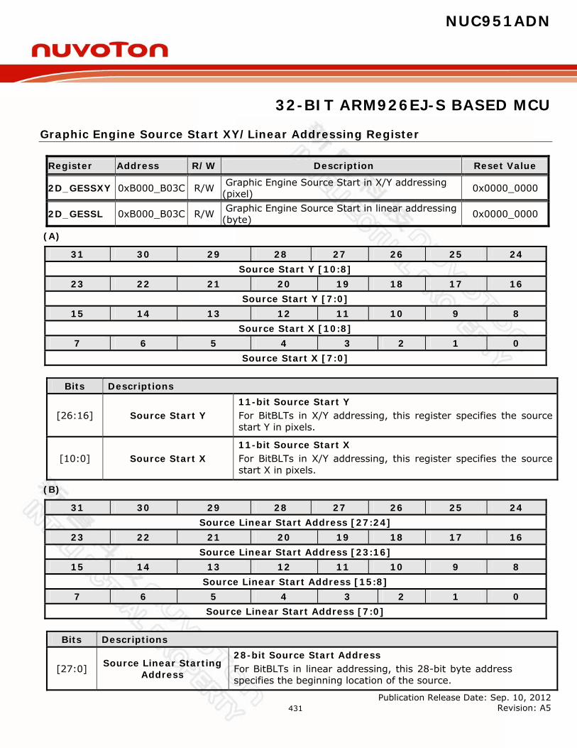
NUC951ADN
32-BIT ARM926EJ-S BASED MCU
Publication Release Date: Sep. 10, 2012 Revision: A5
431
Graphic Engine Source Start XY/Linear Addressing Register
Register Address R/W Description Reset Value
2D_GESSXY 0xB000_B03C R/W Graphic Engine Source Start in X/Y addressing (pixel) 0x0000_0000
2D_GESSL 0xB000_B03C R/W Graphic Engine Source Start in linear addressing (byte) 0x0000_0000
(A)
Bits Descriptions
[26:16] Source Start Y 11-bit Source Start Y For BitBLTs in X/Y addressing, this register specifies the source start Y in pixels.
[10:0] Source Start X 11-bit Source Start X For BitBLTs in X/Y addressing, this register specifies the source start X in pixels.
(B)
Bits Descriptions
[27:0] Source Linear Starting Address
28-bit Source Start Address For BitBLTs in linear addressing, this 28-bit byte address specifies the beginning location of the source.
31 30 29 28 27 26 25 24 Source Start Y [10:8]
23 22 21 20 19 18 17 16 Source Start Y [7:0]
15 14 13 12 11 10 9 8 Source Start X [10:8]
7 6 5 4 3 2 1 0 Source Start X [7:0]
31 30 29 28 27 26 25 24 Source Linear Start Address [27:24]
23 22 21 20 19 18 17 16 Source Linear Start Address [23:16]
15 14 13 12 11 10 9 8 Source Linear Start Address [15:8]
7 6 5 4 3 2 1 0 Source Linear Start Address [7:0]

NUC951ADN
32-BIT ARM926EJ-S BASED MCU
Publication Release Date: Sep. 10, 2012 Revision: A5
432
Graphic Engine Destination Start XY/Linear Register
Register Address R/W Description Reset Value
2D_GEDSXY 0xB000_B040 R/W Graphic Engine Destination Start X/Y addressing (pixel) 0x0000_0000
2D_GEDSL 0xB000_B040 R/W Graphic Engine Destination Start Linear address (byte) 0x0000_0000
(A)
Bits Descriptions
[26:16] Destination Start Y
11-bit Destination Start Y For BitBLTs and Bresenham line draw in X/Y addressing, this register specifies the destination start Y in pixels.
[10:0] Destination Start X 11-bit Destination Start X For BitBLTs and Bresenham line draw in X/Y addressing, this register specifies the destination start X in pixels.
31 30 29 28 27 26 25 24 Destination Start Y [10:8]
23 22 21 20 19 18 17 16 Destination Start Y [7:0]
15 14 13 12 11 10 9 8 Destination Start X [10:8]
7 6 5 4 3 2 1 0 Destination Start X [7:0]

NUC951ADN
32-BIT ARM926EJ-S BASED MCU
Publication Release Date: Sep. 10, 2012 Revision: A5
433
(B)
Bits Descriptions
[27:0] Destination Linear Starting Address
28-bit Destination Linear Starting Address For BitBLTs in linear addressing mode, this register specifies the destination linear starting address in bytes.
31 30 29 28 27 26 25 24 Destination Linear Start Address [27:24]
23 22 21 20 19 18 17 16 Destination Linear Start Address [23:16]
15 14 13 12 11 10 9 8 Destination Linear Start Address [15:8]
7 6 5 4 3 2 1 0 Destination Linear Start Address [7:0]
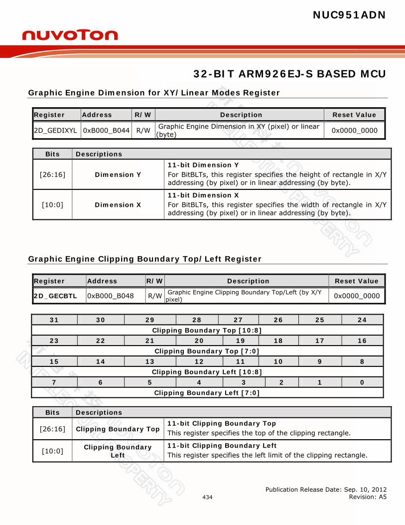
NUC951ADN
32-BIT ARM926EJ-S BASED MCU
Publication Release Date: Sep. 10, 2012 Revision: A5
434
Graphic Engine Dimension for XY/Linear Modes Register
Register Address R/W Description Reset Value
2D_GEDIXYL 0xB000_B044 R/W Graphic Engine Dimension in XY (pixel) or linear (byte) 0x0000_0000
Bits Descriptions
[26:16] Dimension Y 11-bit Dimension Y For BitBLTs, this register specifies the height of rectangle in X/Y addressing (by pixel) or in linear addressing (by byte).
[10:0] Dimension X 11-bit Dimension X For BitBLTs, this register specifies the width of rectangle in X/Y addressing (by pixel) or in linear addressing (by byte).
Graphic Engine Clipping Boundary Top/Left Register
Register Address R/W Description Reset Value
2D_GECBTL 0xB000_B048 R/W Graphic Engine Clipping Boundary Top/Left (by X/Y pixel) 0x0000_0000
Bits Descriptions
[26:16] Clipping Boundary Top 11-bit Clipping Boundary Top This register specifies the top of the clipping rectangle.
[10:0] Clipping Boundary Left
11-bit Clipping Boundary Left This register specifies the left limit of the clipping rectangle.
31 30 29 28 27 26 25 24 Clipping Boundary Top [10:8]
23 22 21 20 19 18 17 16 Clipping Boundary Top [7:0]
15 14 13 12 11 10 9 8 Clipping Boundary Left [10:8]
7 6 5 4 3 2 1 0 Clipping Boundary Left [7:0]
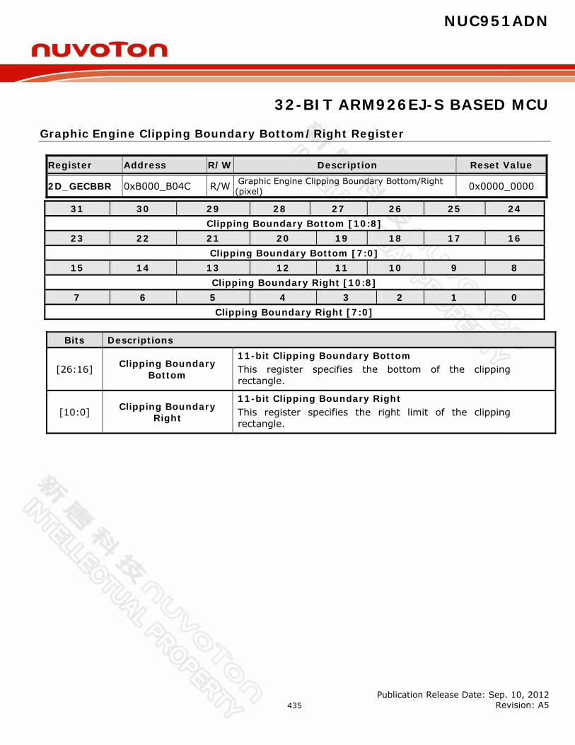
NUC951ADN
32-BIT ARM926EJ-S BASED MCU
Publication Release Date: Sep. 10, 2012 Revision: A5
435
Graphic Engine Clipping Boundary Bottom/Right Register
Register Address R/W Description Reset Value
2D_GECBBR 0xB000_B04C R/W Graphic Engine Clipping Boundary Bottom/Right (pixel) 0x0000_0000
Bits Descriptions
[26:16] Clipping Boundary Bottom
11-bit Clipping Boundary Bottom This register specifies the bottom of the clipping rectangle.
[10:0] Clipping Boundary Right
11-bit Clipping Boundary Right This register specifies the right limit of the clipping rectangle.
31 30 29 28 27 26 25 24 Clipping Boundary Bottom [10:8]
23 22 21 20 19 18 17 16 Clipping Boundary Bottom [7:0]
15 14 13 12 11 10 9 8 Clipping Boundary Right [10:8]
7 6 5 4 3 2 1 0 Clipping Boundary Right [7:0]
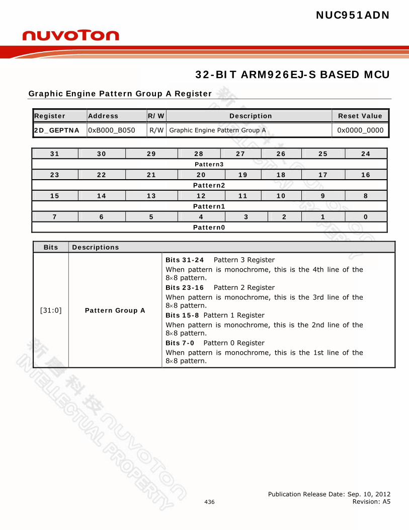
NUC951ADN
32-BIT ARM926EJ-S BASED MCU
Publication Release Date: Sep. 10, 2012 Revision: A5
436
Graphic Engine Pattern Group A Register
Register Address R/W Description Reset Value
2D_GEPTNA 0xB000_B050 R/W Graphic Engine Pattern Group A 0x0000_0000
Bits Descriptions
[31:0] Pattern Group A
Bits 31-24 Pattern 3 Register When pattern is monochrome, this is the 4th line of the 88 pattern. Bits 23-16 Pattern 2 Register When pattern is monochrome, this is the 3rd line of the 88 pattern. Bits 15-8 Pattern 1 Register When pattern is monochrome, this is the 2nd line of the 88 pattern. Bits 7-0 Pattern 0 Register When pattern is monochrome, this is the 1st line of the 88 pattern.
31 30 29 28 27 26 25 24 Pattern3
23 22 21 20 19 18 17 16 Pattern2
15 14 13 12 11 10 9 8 Pattern1
7 6 5 4 3 2 1 0 Pattern0
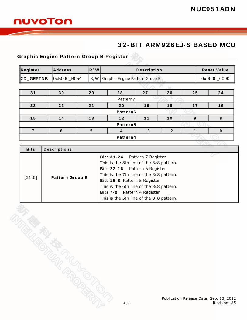
NUC951ADN
32-BIT ARM926EJ-S BASED MCU
Publication Release Date: Sep. 10, 2012 Revision: A5
437
Graphic Engine Pattern Group B Register
Register Address R/W Description Reset Value
2D_GEPTNB 0xB000_B054 R/W Graphic Engine Pattern Group B 0x0000_0000
Bits Descriptions
[31:0] Pattern Group B
Bits 31-24 Pattern 7 Register This is the 8th line of the 88 pattern. Bits 23-16 Pattern 6 Register This is the 7th line of the 88 pattern. Bits 15-8 Pattern 5 Register This is the 6th line of the 88 pattern. Bits 7-0 Pattern 4 Register This is the 5th line of the 88 pattern.
31 30 29 28 27 26 25 24 Pattern7
23 22 21 20 19 18 17 16 Pattern6
15 14 13 12 11 10 9 8 Pattern5
7 6 5 4 3 2 1 0 Pattern4

NUC951ADN
32-BIT ARM926EJ-S BASED MCU
Publication Release Date: Sep. 10, 2012 Revision: A5
438
Graphic Engine Write Plane Mask Register
Register Address R/W Description Reset Value
2D_GEWPM 0xB000_B058 R/W Graphic Engine Write Plane Mask 0x0000_0000
Bits Descriptions
[23:0] Write Plane Mask
24-bit Write Plane Mask These bits specify which bits within each pixel are subject to update by the Graphics Engine. A one enable writing to the corresponding bit plane and a 0 inhibits writing to the corresponding bit plane. Only the corresponding number of bits-per-pixel in the display mode is required in the register.
31 30 29 28 27 26 25 24 Reserved
23 22 21 20 19 18 17 16 Write Plane Mask [23:16]
15 14 13 12 11 10 9 8 Write Plane Mask [15:8]
7 6 5 4 3 2 1 0 Write Plane Mask [7:0]
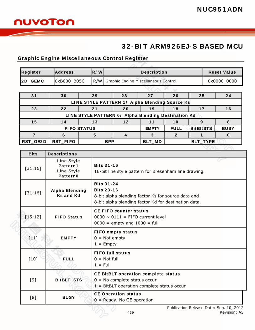
NUC951ADN
32-BIT ARM926EJ-S BASED MCU
Publication Release Date: Sep. 10, 2012 Revision: A5
439
Graphic Engine Miscellaneous Control Register
Register Address R/W Description Reset Value
2D_GEMC 0xB000_B05C R/W Graphic Engine Miscellaneous Control 0x0000_0000
Bits Descriptions
[31:16]
Line Style Pattern1 Line Style Pattern0
Bits 31-16 16-bit line style pattern for Bresenham line drawing.
[31:16] Alpha Blending Ks and Kd
Bits 31-24 Bits 23-16 8-bit alpha blending factor Ks for source data and 8-bit alpha blending factor Kd for destination data.
[15:12] FIFO Status GE FIFO counter status 0000 ~ 0111 = FIFO current level 0000 = empty and 1000 = full
[11] EMPTY FIFO empty status 0 = Not empty 1 = Empty
[10] FULL FIFO full status 0 = Not full 1 = Full
[9] BitBLT_STS GE BitBLT operation complete status 0 = No complete status occur 1 = BitBLT operation complete status occur
[8] BUSY GE Operation status 0 = Ready, No GE operation
31 30 29 28 27 26 25 24 LINE STYLE PATTERN 1/ Alpha Blending Source Ks
23 22 21 20 19 18 17 16 LINE STYLE PATTERN 0/ Alpha Blending Destination Kd
15 14 13 12 11 10 9 8 FIFO STATUS EMPTY FULL BitBltSTS BUSY
7 6 5 4 3 2 1 0 RST_GE2D RST_FIFO BPP BLT_MD BLT_TYPE

NUC951ADN
32-BIT ARM926EJ-S BASED MCU
Publication Release Date: Sep. 10, 2012 Revision: A5
440
1 = Busy, GE operation is still under working
[7] RST_GE2D Bit 7 1 = Reset GE2D.
[6] RST_FIFO Bit 6 1 = Reset FIFO.
[5:4] Bit Per Pixel
Bits 5-4 Graphics Engine Pixel Depth 00 = 8-bit 01 = 16-bit 10 = 32-bit 11 = reserved
[3] BLT_MODE 0 = BitBLT type is according to GEC control bits 1 = BitBLT type follows BLT_TYPE[2:0] setting as below
[2:0] BLT_TYPE
Bits 2-0 BitBLT Type Setting 000 = HostBLT (write mode) 001 = HostBLT (read mode) 010 = SolidFillBLT 011 = PatternBLT 100 = BlockMoveBLT 101 = Color/Font Expansion BLT 110 = Monochrome Transparent BLT 111 = Color Transparent BLT

NUC951ADN
32-BIT ARM926EJ-S BASED MCU
Publication Release Date: Sep. 10, 2012 Revision: A5
441
7.14 UART Controller The Universal Asynchronous Receiver/Transmitter (UART) performs a serial-to-parallel conversion on data characters received from the peripheral such as MODEM, and a parallel-to-serial conversion on data characters received from the CPU. There are five UART blocks and accessory logic in this chip.
7.14.1 UART Feature Description 7.14.1.1 UART0 UART0 is a general UART block without Modem I/O signals.
UART0 Clock Source External Crystal UART Type General UART FIFO Number 16-byte receiving FIFO and 16 byte transmitting FIFO Modem Function None Accessory Function None I/O pin TXD0, RXD0
7.14.1.2 UART1 UART1 is a high speed UART for the Bluetooth transceiver. The FIFO has 64-byte for receiving and 64-byte for transmitting. The clock source is programmable in chip clock generator.
UART1 Clock Source External Crystal or internal PLL (Programmable) UART Type High speed UART FIFO Number 64-byte receiving FIFO and 64 byte transmitting FIFO Modem Function CTS and RTS Accessory Function Bluetooth I/O pin TXD1, RXD1, RTS1, CTS1
7.14.1.3 UART2 UART2 is a general UART with IrDA SIR.
UART2 Clock Source External Crystal UART Type General UART FIFO Number 16-byte receiving FIFO and 16 byte transmitting FIFO Modem Function none Accessory Function IrDA SIR I/O pin TXD2, RXD2
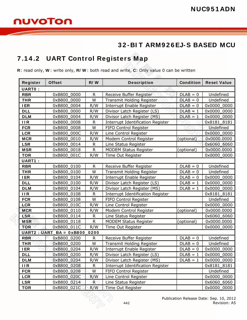
NUC951ADN
32-BIT ARM926EJ-S BASED MCU
Publication Release Date: Sep. 10, 2012 Revision: A5
442
7.14.2 UART Control Registers Map R: read only, W: write only, R/W: both read and write, C: Only value 0 can be written
Register Offset R/W Description Condition Reset Value UART0 : RBR 0xB800_0000 R Receive Buffer Register DLAB = 0 Undefined THR 0xB800_0000 W Transmit Holding Register DLAB = 0 Undefined IER 0xB800_0004 R/W Interrupt Enable Register DLAB = 0 0x0000_0000 DLL 0xB800_0000 R/W Divisor Latch Register (LS) DLAB = 1 0x0000_0000 DLM 0xB800_0004 R/W Divisor Latch Register (MS) DLAB = 1 0x0000_0000 IIR 0xB800_0008 R Interrupt Identification Register 0x8181_8181 FCR 0xB800_0008 W FIFO Control Register Undefined LCR 0xB800_000C R/W Line Control Register 0x0000_0000 MCR 0xB800_0010 R/W Modem Control Register (optional) 0x0000.0000 LSR 0xB800_0014 R Line Status Register 0x6060_6060 MSR 0xB800_0018 R MODEM Status Register (optional) 0x0000.0000 TOR 0xB800_001C R/W Time Out Register 0x0000_0000 UART1 : RBR 0xB800_0100 R Receive Buffer Register DLAB = 0 Undefined THR 0xB800_0100 W Transmit Holding Register DLAB = 0 Undefined IER 0xB800_0104 R/W Interrupt Enable Register DLAB = 0 0x0000_0000 DLL 0xB800_0100 R/W Divisor Latch Register (LS) DLAB = 1 0x0000_0000 DLM 0xB800_0104 R/W Divisor Latch Register (MS) DLAB = 1 0x0000_0000 IIR 0xB800_0108 R Interrupt Identification Register 0x8181_8181 FCR 0xB800_0108 W FIFO Control Register Undefined LCR 0xB800_010C R/W Line Control Register 0x0000_0000 MCR 0xB800_0110 R/W Modem Control Register (optional) 0x0000.0000 LSR 0xB800_0114 R Line Status Register 0x6060_6060 MSR 0xB800_0118 R MODEM Status Register (optional) 0x0000.0000 TOR 0xB800_011C R/W Time Out Register 0x0000_0000 UART2 : UART_BA = 0xB800_0200 RBR 0xB800_0200 R Receive Buffer Register DLAB = 0 Undefined THR 0xB800_0200 W Transmit Holding Register DLAB = 0 Undefined IER 0xB800_0204 R/W Interrupt Enable Register DLAB = 0 0x0000_0000 DLL 0xB800_0200 R/W Divisor Latch Register (LS) DLAB = 1 0x0000_0000 DLM 0xB800_0204 R/W Divisor Latch Register (MS) DLAB = 1 0x0000_0000 IIR 0xB800_0208 R Interrupt Identification Register 0x8181_8181 FCR 0xB800_0208 W FIFO Control Register Undefined LCR 0xB800_020C R/W Line Control Register 0x0000_0000 LSR 0xB800_0214 R Line Status Register 0x6060_6060 TOR 0xB800_021C R/W Time Out Register 0x0000_0000
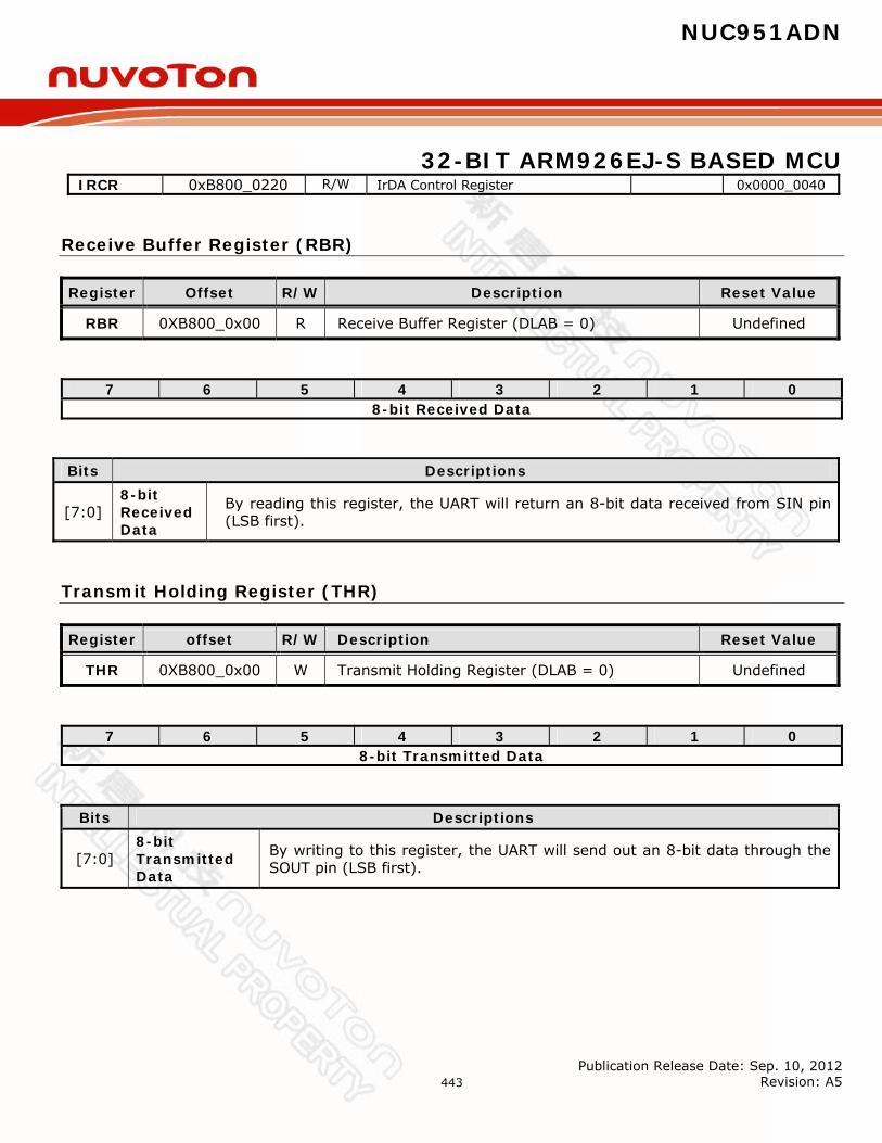
NUC951ADN
32-BIT ARM926EJ-S BASED MCU
Publication Release Date: Sep. 10, 2012 Revision: A5
443
IRCR 0xB800_0220 R/W IrDA Control Register 0x0000_0040
Receive Buffer Register (RBR)
Register Offset R/W Description Reset Value
RBR 0XB800_0x00 R Receive Buffer Register (DLAB = 0) Undefined
7 6 5 4 3 2 1 0 8-bit Received Data
Bits Descriptions
[7:0] 8-bit Received Data
By reading this register, the UART will return an 8-bit data received from SIN pin (LSB first).
Transmit Holding Register (THR)
Register offset R/W Description Reset Value
THR 0XB800_0x00 W Transmit Holding Register (DLAB = 0) Undefined
7 6 5 4 3 2 1 0 8-bit Transmitted Data
Bits Descriptions
[7:0] 8-bit Transmitted Data
By writing to this register, the UART will send out an 8-bit data through the SOUT pin (LSB first).
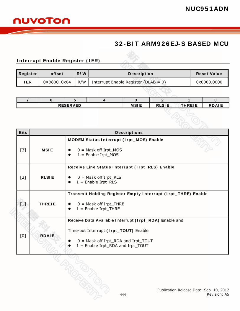
NUC951ADN
32-BIT ARM926EJ-S BASED MCU
Publication Release Date: Sep. 10, 2012 Revision: A5
444
Interrupt Enable Register (IER)
Register offset R/W Description Reset Value
IER 0XB800_0x04 R/W Interrupt Enable Register (DLAB = 0) 0x0000.0000
7 6 5 4 3 2 1 0 RESERVED MSIE RLSIE THREIE RDAIE
Bits Descriptions
[3] MSIE
MODEM Status Interrupt (Irpt_MOS) Enable
0 = Mask off Irpt_MOS 1 = Enable Irpt_MOS
[2] RLSIE
Receive Line Status Interrupt (Irpt_RLS) Enable
0 = Mask off Irpt_RLS 1 = Enable Irpt_RLS
[1] THREIE
Transmit Holding Register Empty Interrupt (Irpt_THRE) Enable
0 = Mask off Irpt_THRE 1 = Enable Irpt_THRE
[0] RDAIE
Receive Data Available Interrupt (Irpt_RDA) Enable and
Time-out Interrupt (Irpt_TOUT) Enable
0 = Mask off Irpt_RDA and Irpt_TOUT 1 = Enable Irpt_RDA and Irpt_TOUT

NUC951ADN
32-BIT ARM926EJ-S BASED MCU
Publication Release Date: Sep. 10, 2012 Revision: A5
445
Divider Latch (Low Byte) Register (DLL)
Register Offset R/W Description Reset Value
DLL 0XB800_0x00 R/W Divisor Latch Register (LS) (DLAB = 1) 0x0000_0000
7 6 5 4 3 2 1 0 Baud Rate Divider (Low Byte)
Bits Descriptions
[7:0] Baud Rate Divisor (Low Byte) The low byte of the baud rate divider
Divisor Latch (High Byte) Register (DLM)
Register Offset R/W Description Reset Value
DLM 0XB800_0x04 R/W Divisor Latch Register (MS) (DLAB = 1) 0x0000_0000
7 6 5 4 3 2 1 0 Baud Rate Divider (High Byte)
Bits Descriptions
[7:0] Baud Rate Divisor (High Byte) The high byte of the baud rate divider
This 16-bit divider DLM, DLL is used to determine the baud rate as follows
Baud Rate = Crystal Clock / 16 * [Divisor + 2]
Note: This definition is different from 16550
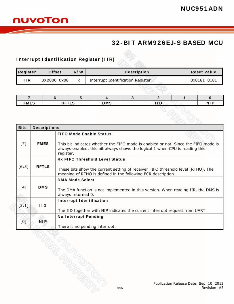
NUC951ADN
32-BIT ARM926EJ-S BASED MCU
Publication Release Date: Sep. 10, 2012 Revision: A5
446
Interrupt Identification Register (IIR)
Register Offset R/W Description Reset Value
IIR 0XB800_0x08 R Interrupt Identification Register 0x8181_8181
7 6 5 4 3 2 1 0 FMES RFTLS DMS IID NIP
Bits Descriptions
[7] FMES
FIFO Mode Enable Status
This bit indicates whether the FIFO mode is enabled or not. Since the FIFO mode is always enabled, this bit always shows the logical 1 when CPU is reading this register.
[6:5] RFTLS
Rx FIFO Threshold Level Status
These bits show the current setting of receiver FIFO threshold level (RTHO). The meaning of RTHO is defined in the following FCR description.
[4] DMS
DMA Mode Select
The DMA function is not implemented in this version. When reading IIR, the DMS is always returned 0.
[3:1] IID Interrupt Identification
The IID together with NIP indicates the current interrupt request from UART.
[0] NIP No Interrupt Pending
There is no pending interrupt.
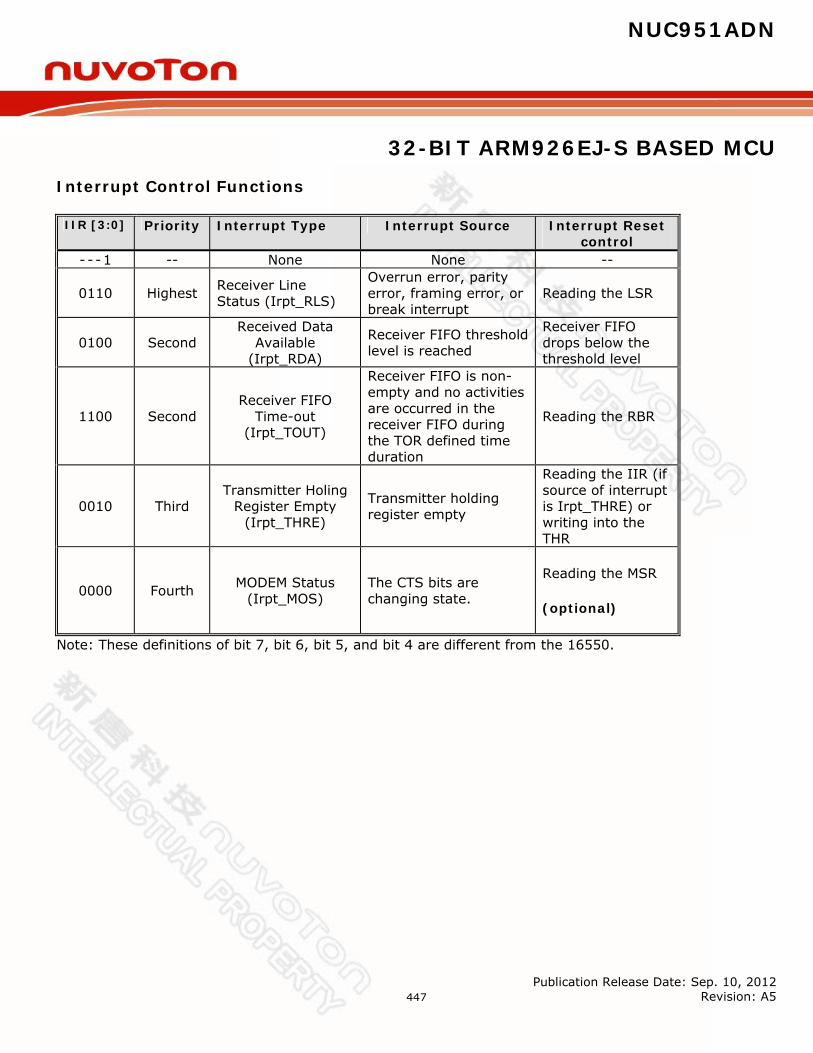
NUC951ADN
32-BIT ARM926EJ-S BASED MCU
Publication Release Date: Sep. 10, 2012 Revision: A5
447
Interrupt Control Functions
IIR [3:0] Priority Interrupt Type Interrupt Source Interrupt Reset control
- - - 1 -- None None --
0110 Highest Receiver Line Status (Irpt_RLS)
Overrun error, parity error, framing error, or break interrupt
Reading the LSR
0100 Second Received Data
Available (Irpt_RDA)
Receiver FIFO threshold level is reached
Receiver FIFO drops below the threshold level
1100 Second Receiver FIFO
Time-out (Irpt_TOUT)
Receiver FIFO is non-empty and no activities are occurred in the receiver FIFO during the TOR defined time duration
Reading the RBR
0010 Third Transmitter Holing
Register Empty (Irpt_THRE)
Transmitter holding register empty
Reading the IIR (if source of interrupt is Irpt_THRE) or writing into the THR
0000 Fourth MODEM Status (Irpt_MOS)
The CTS bits are changing state.
Reading the MSR
(optional)
Note: These definitions of bit 7, bit 6, bit 5, and bit 4 are different from the 16550.
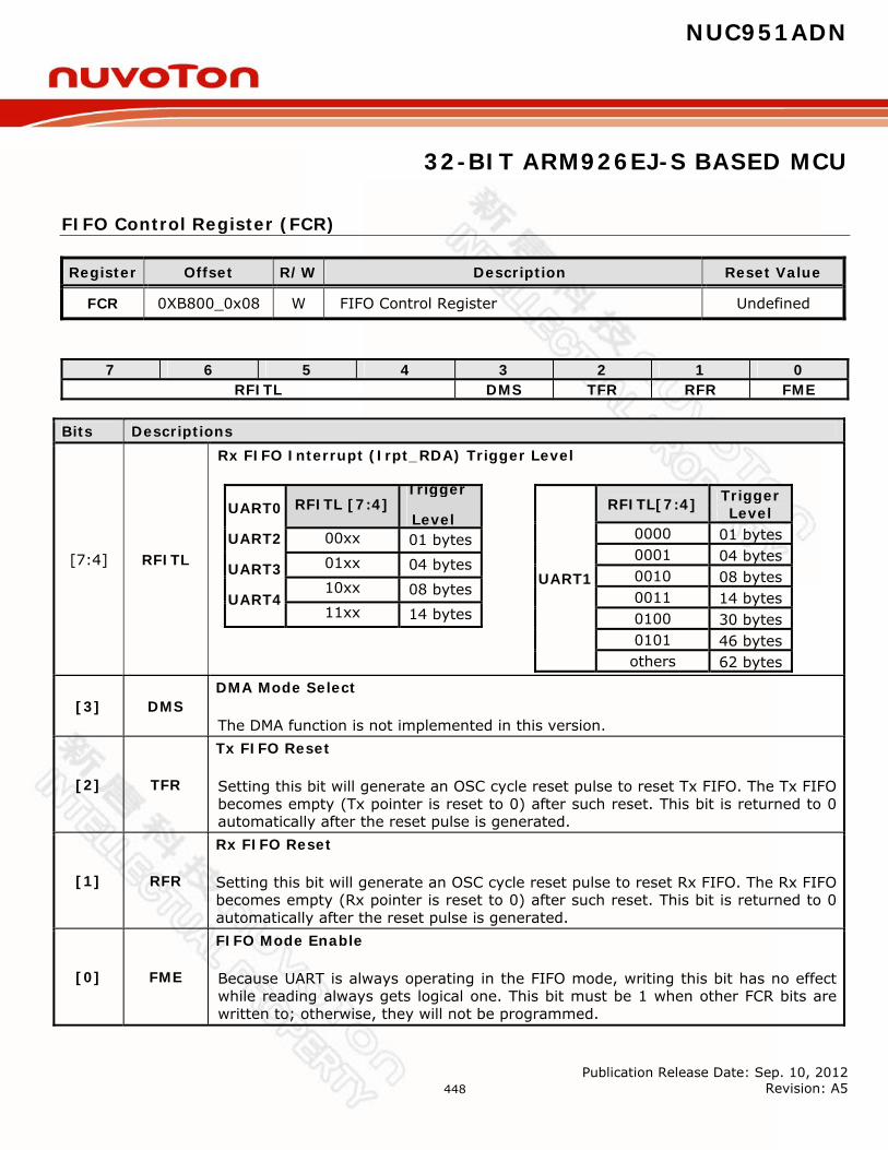
NUC951ADN
32-BIT ARM926EJ-S BASED MCU
Publication Release Date: Sep. 10, 2012 Revision: A5
448
FIFO Control Register (FCR)
Register Offset R/W Description Reset Value
FCR 0XB800_0x08 W FIFO Control Register Undefined
7 6 5 4 3 2 1 0 RFITL DMS TFR RFR FME
Bits Descriptions
[7:4] RFITL
Rx FIFO Interrupt (Irpt_RDA) Trigger Level
UART0
UART2
UART3
UART4
RFITL [7:4] Trigger
Level 00xx 01 bytes 01xx 04 bytes 10xx 08 bytes 11xx 14 bytes
UART1
RFITL[7:4] Trigger Level
0000 01 bytes 0001 04 bytes 0010 08 bytes 0011 14 bytes 0100 30 bytes 0101 46 bytes others 62 bytes
[3] DMS DMA Mode Select
The DMA function is not implemented in this version.
[2] TFR
Tx FIFO Reset
Setting this bit will generate an OSC cycle reset pulse to reset Tx FIFO. The Tx FIFO becomes empty (Tx pointer is reset to 0) after such reset. This bit is returned to 0 automatically after the reset pulse is generated.
[1] RFR
Rx FIFO Reset
Setting this bit will generate an OSC cycle reset pulse to reset Rx FIFO. The Rx FIFO becomes empty (Rx pointer is reset to 0) after such reset. This bit is returned to 0 automatically after the reset pulse is generated.
[0] FME
FIFO Mode Enable
Because UART is always operating in the FIFO mode, writing this bit has no effect while reading always gets logical one. This bit must be 1 when other FCR bits are written to; otherwise, they will not be programmed.
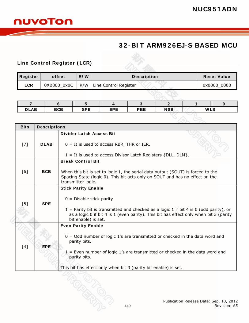
NUC951ADN
32-BIT ARM926EJ-S BASED MCU
Publication Release Date: Sep. 10, 2012 Revision: A5
449
Line Control Register (LCR)
Register offset R/W Description Reset Value
LCR 0XB800_0x0C R/W Line Control Register 0x0000_0000
7 6 5 4 3 2 1 0 DLAB BCB SPE EPE PBE NSB WLS
Bits Descriptions
[7] DLAB
Divider Latch Access Bit
0 = It is used to access RBR, THR or IER.
1 = It is used to access Divisor Latch Registers DLL, DLM.
[6] BCB
Break Control Bit
When this bit is set to logic 1, the serial data output (SOUT) is forced to the Spacing State (logic 0). This bit acts only on SOUT and has no effect on the transmitter logic.
[5] SPE
Stick Parity Enable
0 = Disable stick parity
1 = Parity bit is transmitted and checked as a logic 1 if bit 4 is 0 (odd parity), or as a logic 0 if bit 4 is 1 (even parity). This bit has effect only when bit 3 (parity bit enable) is set.
[4] EPE
Even Parity Enable
0 = Odd number of logic 1’s are transmitted or checked in the data word and parity bits.
1 = Even number of logic 1’s are transmitted or checked in the data word and parity bits.
This bit has effect only when bit 3 (parity bit enable) is set.
NUC951ADN
32-BIT ARM926EJ-S BASED MCU
Publication Release Date: Sep. 10, 2012 Revision: A5
450
[3] PBE
Parity Bit Enable
0 = Parity bit is not generated (transmit data) or checked (receive data) during transfer.
1 = Parity bit is generated or checked between the "last data word bit" and "stop bit" of the serial data.
[2] NSB
Number of “STOP bit”
0= One “ STOP bit” is generated in the transmitted data
1= One and a half “ STOP bit” is generated in the transmitted data when 5-bit word length is selected;
Two “ STOP bit” is generated when 6-, 7- and 8-bit word length is selected.
[1:0] WLS
Word Length Select
WLS[1:0] Character length 00 5 bits 01 6 bits 10 7 bits 11 8 bits
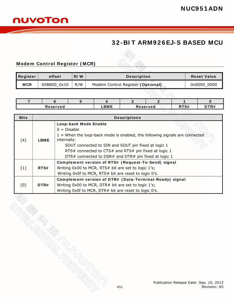
NUC951ADN
32-BIT ARM926EJ-S BASED MCU
Publication Release Date: Sep. 10, 2012 Revision: A5
451
Modem Control Register (MCR)
Register offset R/W Description Reset Value
MCR 0XB800_0x10 R/W Modem Control Register (Optional) 0x0000_0000
7 6 5 4 3 2 1 0 Reserved LBME Reserved RTS# DTR#
Bits Descriptions
[4] LBME
Loop-back Mode Enable 0 = Disable 1 = When the loop-back mode is enabled, the following signals are connected internally:
SOUT connected to SIN and SOUT pin fixed at logic 1 RTS# connected to CTS# and RTS# pin fixed at logic 1 DTR# connected to DSR# and DTR# pin fixed at logic 1
[1] RTS# Complement version of RTS# (Request-To-Send) signal Writing 0x00 to MCR, RTS# bit are set to logic 1’s; Writing 0x0f to MCR, RTS# bit are reset to logic 0’s.
[0] DTR# Complement version of DTR# (Data-Terminal-Ready) signal Writing 0x00 to MCR, DTR# bit are set to logic 1’s; Writing 0x0f to MCR, DTR# bit are reset to logic 0’s.
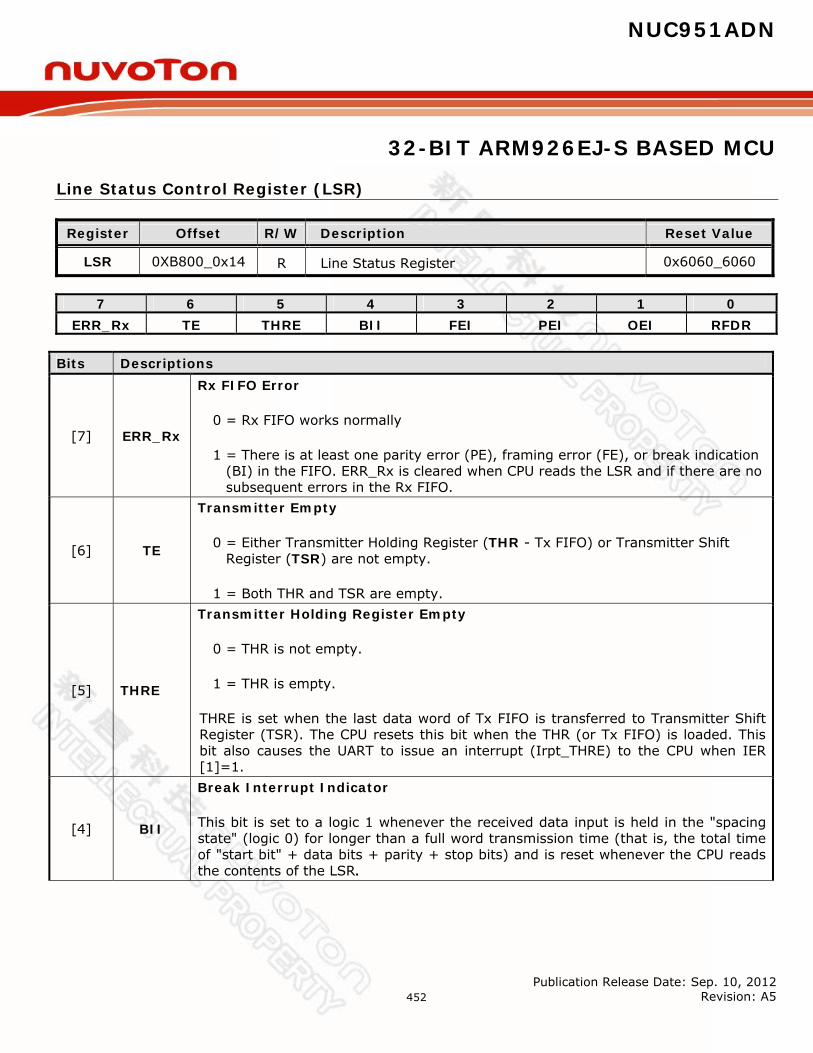
NUC951ADN
32-BIT ARM926EJ-S BASED MCU
Publication Release Date: Sep. 10, 2012 Revision: A5
452
Line Status Control Register (LSR)
Register Offset R/W Description Reset Value
LSR 0XB800_0x14 R Line Status Register 0x6060_6060
7 6 5 4 3 2 1 0
ERR_Rx TE THRE BII FEI PEI OEI RFDR Bits Descriptions
[7] ERR_Rx
Rx FIFO Error
0 = Rx FIFO works normally
1 = There is at least one parity error (PE), framing error (FE), or break indication (BI) in the FIFO. ERR_Rx is cleared when CPU reads the LSR and if there are no subsequent errors in the Rx FIFO.
[6] TE
Transmitter Empty
0 = Either Transmitter Holding Register (THR - Tx FIFO) or Transmitter Shift Register (TSR) are not empty.
1 = Both THR and TSR are empty.
[5] THRE
Transmitter Holding Register Empty
0 = THR is not empty.
1 = THR is empty.
THRE is set when the last data word of Tx FIFO is transferred to Transmitter Shift Register (TSR). The CPU resets this bit when the THR (or Tx FIFO) is loaded. This bit also causes the UART to issue an interrupt (Irpt_THRE) to the CPU when IER [1]=1.
[4] BII
Break Interrupt Indicator
This bit is set to a logic 1 whenever the received data input is held in the "spacing state" (logic 0) for longer than a full word transmission time (that is, the total time of "start bit" + data bits + parity + stop bits) and is reset whenever the CPU reads the contents of the LSR.
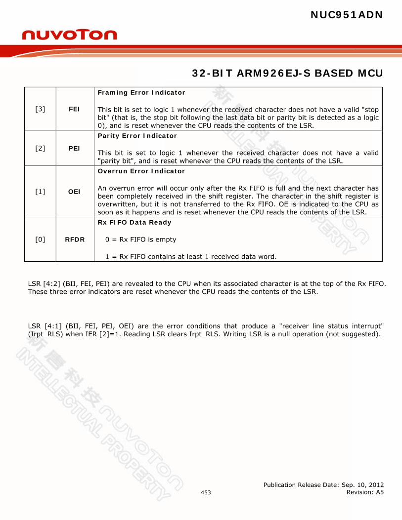
NUC951ADN
32-BIT ARM926EJ-S BASED MCU
Publication Release Date: Sep. 10, 2012 Revision: A5
453
[3] FEI
Framing Error Indicator
This bit is set to logic 1 whenever the received character does not have a valid "stop bit" (that is, the stop bit following the last data bit or parity bit is detected as a logic 0), and is reset whenever the CPU reads the contents of the LSR.
[2] PEI
Parity Error Indicator
This bit is set to logic 1 whenever the received character does not have a valid "parity bit", and is reset whenever the CPU reads the contents of the LSR.
[1] OEI
Overrun Error Indicator
An overrun error will occur only after the Rx FIFO is full and the next character has been completely received in the shift register. The character in the shift register is overwritten, but it is not transferred to the Rx FIFO. OE is indicated to the CPU as soon as it happens and is reset whenever the CPU reads the contents of the LSR.
[0] RFDR
Rx FIFO Data Ready
0 = Rx FIFO is empty
1 = Rx FIFO contains at least 1 received data word.
LSR [4:2] (BII, FEI, PEI) are revealed to the CPU when its associated character is at the top of the Rx FIFO. These three error indicators are reset whenever the CPU reads the contents of the LSR.
LSR [4:1] (BII, FEI, PEI, OEI) are the error conditions that produce a "receiver line status interrupt" (Irpt_RLS) when IER [2]=1. Reading LSR clears Irpt_RLS. Writing LSR is a null operation (not suggested).
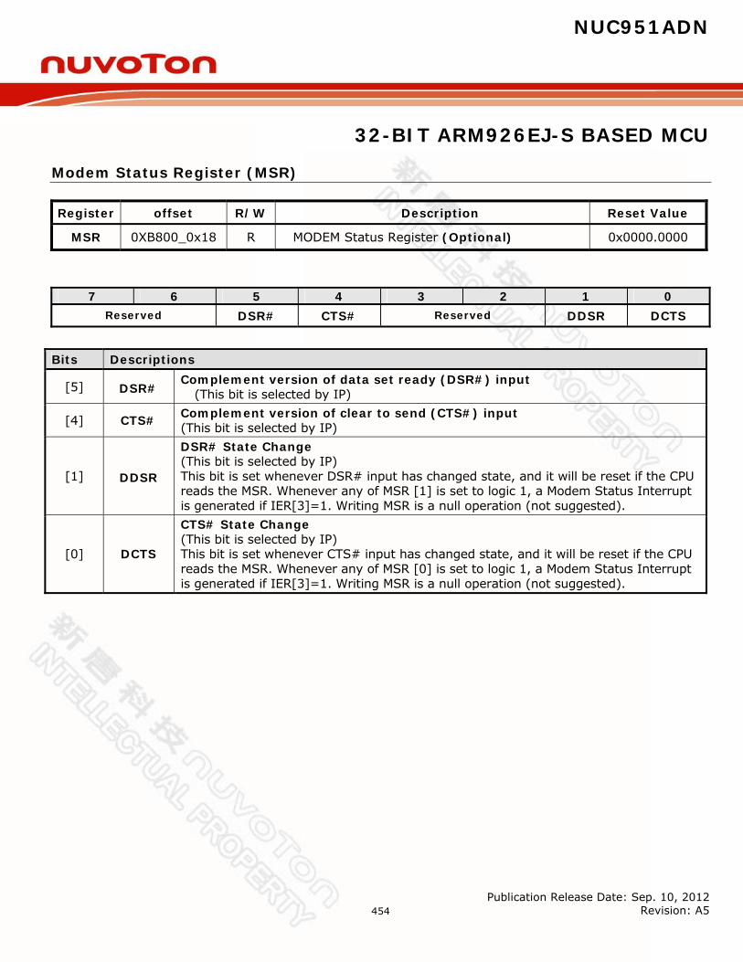
NUC951ADN
32-BIT ARM926EJ-S BASED MCU
Publication Release Date: Sep. 10, 2012 Revision: A5
454
Modem Status Register (MSR)
Register offset R/W Description Reset Value
MSR 0XB800_0x18 R MODEM Status Register (Optional) 0x0000.0000
7 6 5 4 3 2 1 0 Reserved DSR# CTS# Reserved DDSR DCTS
Bits Descriptions
[5] DSR# Complement version of data set ready (DSR#) input
(This bit is selected by IP)
[4] CTS# Complement version of clear to send (CTS#) input (This bit is selected by IP)
[1] DDSR
DSR# State Change (This bit is selected by IP) This bit is set whenever DSR# input has changed state, and it will be reset if the CPU reads the MSR. Whenever any of MSR [1] is set to logic 1, a Modem Status Interrupt is generated if IER[3]=1. Writing MSR is a null operation (not suggested).
[0] DCTS
CTS# State Change (This bit is selected by IP) This bit is set whenever CTS# input has changed state, and it will be reset if the CPU reads the MSR. Whenever any of MSR [0] is set to logic 1, a Modem Status Interrupt is generated if IER[3]=1. Writing MSR is a null operation (not suggested).
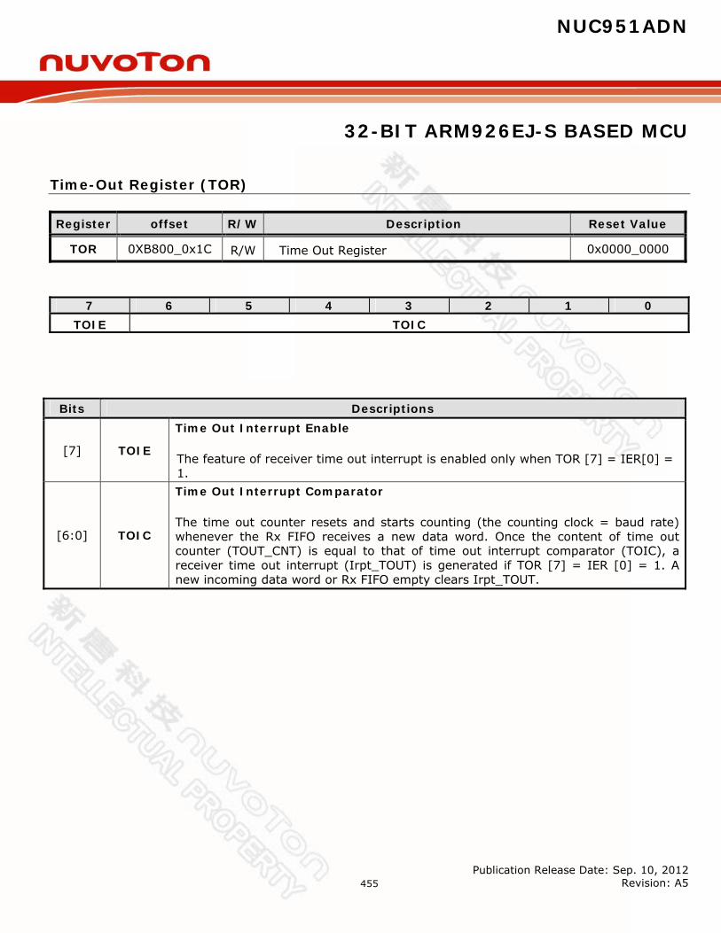
NUC951ADN
32-BIT ARM926EJ-S BASED MCU
Publication Release Date: Sep. 10, 2012 Revision: A5
455
Time-Out Register (TOR)
Register offset R/W Description Reset Value
TOR 0XB800_0x1C R/W Time Out Register 0x0000_0000
7 6 5 4 3 2 1 0 TOIE TOIC
Bits Descriptions
[7] TOIE
Time Out Interrupt Enable
The feature of receiver time out interrupt is enabled only when TOR [7] = IER[0] = 1.
[6:0] TOIC
Time Out Interrupt Comparator
The time out counter resets and starts counting (the counting clock = baud rate) whenever the Rx FIFO receives a new data word. Once the content of time out counter (TOUT_CNT) is equal to that of time out interrupt comparator (TOIC), a receiver time out interrupt (Irpt_TOUT) is generated if TOR [7] = IER [0] = 1. A new incoming data word or Rx FIFO empty clears Irpt_TOUT.

NUC951ADN
32-BIT ARM926EJ-S BASED MCU
Publication Release Date: Sep. 10, 2012 Revision: A5
456
IrDA Control Register (IRCR)
Register Offset R/W Description Reset Value
IRCR 0xB800_0220 R/W IrDA Control Register for UART2 0x0000_0040
7 6 5 4 3 2 1 0 Reserved INV_Rx INV_Tx Reserved Tx_SELECT IrDA_EN
Bits Descriptions
[6] INV_Rx INV_Rx 1: Inverse Rx input signal 0: No inversion
[5] INV_Tx INV_Tx 1: Inverse Tx output signal 0: No inversion
[1] Tx_SELECT Tx_SELECT 1: Enable IrDA transmitter 0: Enable IrDA receiver
[0] IrDA_EN IrDA_EN 1: Enable IrDA block 0: Disable IrDA block

NUC951ADN
32-BIT ARM926EJ-S BASED MCU
Publication Release Date: Sep. 10, 2012 Revision: A5
457
7.15 TIMER Controller
7.15.1 General Timer Controller The timer module includes five channels, TIMER0~TIMER4, they can easily be implemented as counting scheme. The timer can perform functions like frequency measurement, event counting, interval measurement, pulse generation, delay timing, and so on. The timer possesses features such as adjustable resolution, programmable counting period, and detailed information. The timer can generate an interrupt signal upon timeout, or provide the current value of count during operation. The general TIMER Controller includes the following features Five channels with a 24-bit down counter and an interrupt request each Independent clock source for each channel Maximum uninterrupted time = (1 / 15 MHz) * (255) * (2^24 - 1), if TCLK = 15 MHz
7.15.2 Watchdog Timer The purpose of watchdog timer is to perform a system restart after the software running into a problem. This prevents system from hanging for an indefinite period of time. It is a free running timer with programmable time-out intervals. When the specified time internal expires, a system reset can be generated. If the watchdog timer reset function is enabled and the watchdog timer is not being reset before timing out, then the watchdog reset is activated after 1024 WDT clocks. Setting WTE in the register WTCR enables the watchdog timer. The WTR should be set before making use of watchdog timer. This ensures that the watchdog timer restarts from a know state. The watchdog timer will start counting and time-out after a specified period of time. The time-out interval is selected by two bits, WTIS[1:0]. The WTR is self-clearing, i.e., after setting it, the hardware will automatically reset it. When timeout occurs, Watchdog Timer interrupt flag is set. Watchdog Timer waits for an additional 1024 WDT clock cycles before issuing a reset signal, if the WTRE is set. The WTRF will be set and the reset signal will last for 15 WDT clock cycles long. When used as a simple timer, the interrupt and reset functions are disabled. Watchdog Timer will set the WTIF each time a timeout occurs. The WTIF can be polled to check the status, and software can restart the timer by setting the WTR.

NUC951ADN
32-BIT ARM926EJ-S BASED MCU
Publication Release Date: Sep. 10, 2012 Revision: A5
458
7.15.3 Timer Control Registers Map R: read only, W: write only, R/W: both read and write, C: Only value 0 can be written
Register Address R/W/C Description Reset Value
TMR_BA = 0xB800_1000
TCSR0 0xB800_1000 R/W Timer Control and Status Register 0 0x0000_0005
TCSR1 0xB800_1004 R/W Timer Control and Status Register 1 0x0000_0005
TICR0 0xB800_1008 R/W Timer Initial Control Register 0 0x0000_0000
TICR1 0xB800_100C R/W Timer Initial Control Register 1 0x0000_0000
TDR0 0xB800_1010 R Timer Data Register 0 0x0000_0000
TDR1 0xB800_1014 R Timer Data Register 1 0x0000_0000
TISR 0xB800_1018 R/C Timer Interrupt Status Register 0x0000_0000
WTCR 0xB800_101C R/W Watchdog Timer Control Register 0x0000_0400
TCSR2 0xB800_1020 R/W Timer Control and Status Register 2 0x0000_0005
TCSR3 0xB800_1024 R/W Timer Control and Status Register 3 0x0000_0005
TICR2 0xB800_1028 R/W Timer Initial Control Register 2 0x0000_0000
TICR3 0xB800_102C R/W Timer Initial Control Register 3 0x0000_0000
TDR2 0xB800_1030 R Timer Data Register 2 0x0000_0000
TDR3 0xB800_1034 R Timer Data Register 3 0x0000_0000
TCSR4 0xB800_1040 R/W Timer Control and Status Register 4 0x0000_0005
TICR4 0xB800_1048 R/W Timer Initial Control Register 4 0x0000_0000
TDR4 0xB800_1050 R Timer Data Register 4 0x0000_0000

NUC951ADN
32-BIT ARM926EJ-S BASED MCU
Publication Release Date: Sep. 10, 2012 Revision: A5
459
Timer Control and Status Register 0~4 (TCR0~TCR4)
Register Address R/W/C Description Reset Value
TCSR0 0xB800_1000 R/W Timer Control and Status Register 0 0x0000_0005
TCSR1 0xB800_1004 R/W Timer Control and Status Register 1 0x0000_0005
TCSR2 0xB800_1020 R/W Timer Control and Status Register 2 0x0000_0005
TCSR3 0xB800_1024 R/W Timer Control and Status Register 3 0x0000_0005
TCSR4 0xB800_1040 R/W Timer Control and Status Register 4 0x0000_0005
31 30 29 28 27 26 25 24 RESERVED CE IE MODE CRST CACT RESERVED
23 22 21 20 19 18 17 16 RESERVED
15 14 13 12 11 10 9 8 RESERVED
7 6 5 4 3 2 1 0 PRESCALE
Bits Descriptions
[30] CE Counter Enable 0 = Stops counting 1 = Starts counting
[29] IE
Interrupt Enable 0 = Disables timer interrupt 1 = Enables timer interrupt. If timer interrupt is enabled, the timer asserts its interrupt signal when the associated counter decrements to zero.
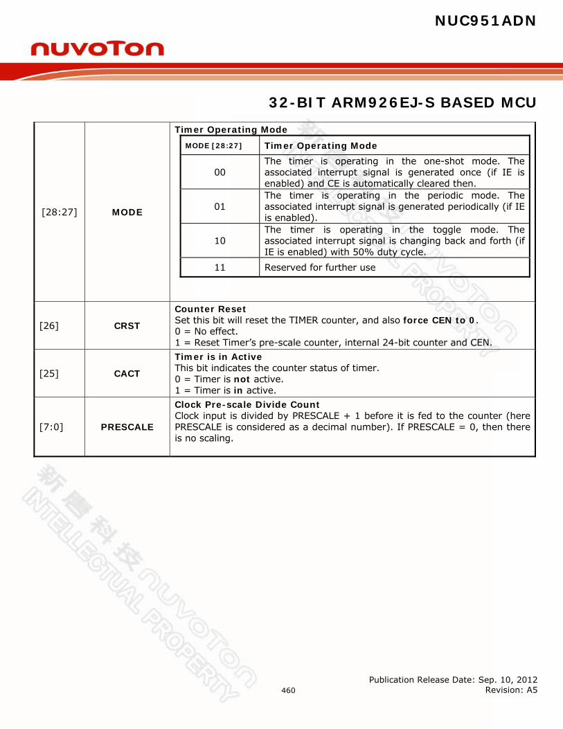
NUC951ADN
32-BIT ARM926EJ-S BASED MCU
Publication Release Date: Sep. 10, 2012 Revision: A5
460
[28:27] MODE
Timer Operating Mode MODE [28:27] Timer Operating Mode
00 The timer is operating in the one-shot mode. The associated interrupt signal is generated once (if IE is enabled) and CE is automatically cleared then.
01 The timer is operating in the periodic mode. The associated interrupt signal is generated periodically (if IE is enabled).
10 The timer is operating in the toggle mode. The associated interrupt signal is changing back and forth (if IE is enabled) with 50% duty cycle.
11 Reserved for further use
[26] CRST
Counter Reset Set this bit will reset the TIMER counter, and also force CEN to 0. 0 = No effect. 1 = Reset Timer’s pre-scale counter, internal 24-bit counter and CEN.
[25] CACT
Timer is in Active This bit indicates the counter status of timer. 0 = Timer is not active. 1 = Timer is in active.
[7:0] PRESCALE
Clock Pre-scale Divide Count Clock input is divided by PRESCALE + 1 before it is fed to the counter (here PRESCALE is considered as a decimal number). If PRESCALE = 0, then there is no scaling.

NUC951ADN
32-BIT ARM926EJ-S BASED MCU
Publication Release Date: Sep. 10, 2012 Revision: A5
461
Timer Initial Count Register 0~4 (TICR0~TICR4)
Register Address R/W/C Description Reset Value
TICR0 0xB800_1008 R/W Timer Initial Control Register 0 0x0000_00FF
TICR1 0xB800_100C R/W Timer Initial Control Register 1 0x0000_00FF
TICR2 0xB800_1028 R/W Timer Initial Control Register 2 0x0000_00FF
TICR3 0xB800_102C R/W Timer Initial Control Register 3 0x0000_00FF
TICR4 0xB800_1048 R/W Timer Initial Control Register 4 0x0000_00FF
31 30 29 28 27 26 25 24 RESERVED
23 22 21 20 19 18 17 16 TIC [23:16]
15 14 13 12 11 10 9 8 TIC [15:8]
7 6 5 4 3 2 1 0 TIC [7:0]
Bits Descriptions
[23:0] TIC
Timer Initial Count This is a 24-bit value representing the initial count. Timer will reload this value whenever the counter is decremented to zero.
NOTE:
(1) Never write 0x0 in TIC, or the core will run into unknown state. (2) No matter CEN is 0 or 1, whenever software write a new value into
this register, Timer will restart counting using this new value and abort previous count.

NUC951ADN
32-BIT ARM926EJ-S BASED MCU
Publication Release Date: Sep. 10, 2012 Revision: A5
462
Timer Data Register 0~4 (TDR0~TDR4)
Register Address R/W/C Description Reset Value
TDR0 0xB800_1010 R Timer Data Register 0 0x0000_00FF
TDR1 0xB800_1014 R Timer Data Register 1 0x0000_00FF
TDR2 0xB800_1030 R Timer Data Register 2 0x0000_00FF
TDR3 0xB800_1034 R Timer Data Register 3 0x0000_00FF
TDR4 0xB800_1050 R Timer Data Register 4 0x0000_00FF
31 30 29 28 27 26 25 24 RESERVED
23 22 21 20 19 18 17 16 TDR [23:16]
15 14 13 12 11 10 9 8 TDR [15:8]
7 6 5 4 3 2 1 0 TDR [7:0]
Bits Descriptions
[23:0] TDR
Timer Data Register The current count is registered in this 24-bit value.
NOTE: Software can read a correct current value on this register only when CEN = 0, or the value represents here could not be a correct one.
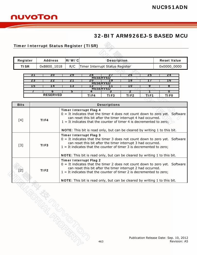
NUC951ADN
32-BIT ARM926EJ-S BASED MCU
Publication Release Date: Sep. 10, 2012 Revision: A5
463
Timer Interrupt Status Register (TISR)
Register Address R/W/C Description Reset Value
TISR 0xB800_1018 R/C Timer Interrupt Status Register 0x0000_0000
31 30 29 28 27 26 25 24 RESERVED
23 22 21 20 19 18 17 16 RESERVED
15 14 13 12 11 10 9 8 RESERVED
7 6 5 4 3 2 1 0 RESERVED TIF4 TIF3 TIF2 TIF1 TIF0
Bits Descriptions
[4] TIF4
Timer Interrupt Flag 4 0 = It indicates that the timer 4 does not count down to zero yet. Software
can reset this bit after the timer interrupt 4 had occurred. 1 = It indicates that the counter of timer 4 is decremented to zero;
NOTE: This bit is read only, but can be cleared by writing 1 to this bit.
[3] TIF3
Timer Interrupt Flag 3 0 = It indicates that the timer 3 does not count down to zero yet. Software
can reset this bit after the timer interrupt 3 had occurred. 1 = It indicates that the counter of timer 3 is decremented to zero;
NOTE: This bit is read only, but can be cleared by writing 1 to this bit.
[2] TIF2
Timer Interrupt Flag 2 0 = It indicates that the timer 2 does not count down to zero yet. Software
can reset this bit after the timer interrupt 2 had occurred. 1 = It indicates that the counter of timer 2 is decremented to zero;
NOTE: This bit is read only, but can be cleared by writing 1 to this bit.
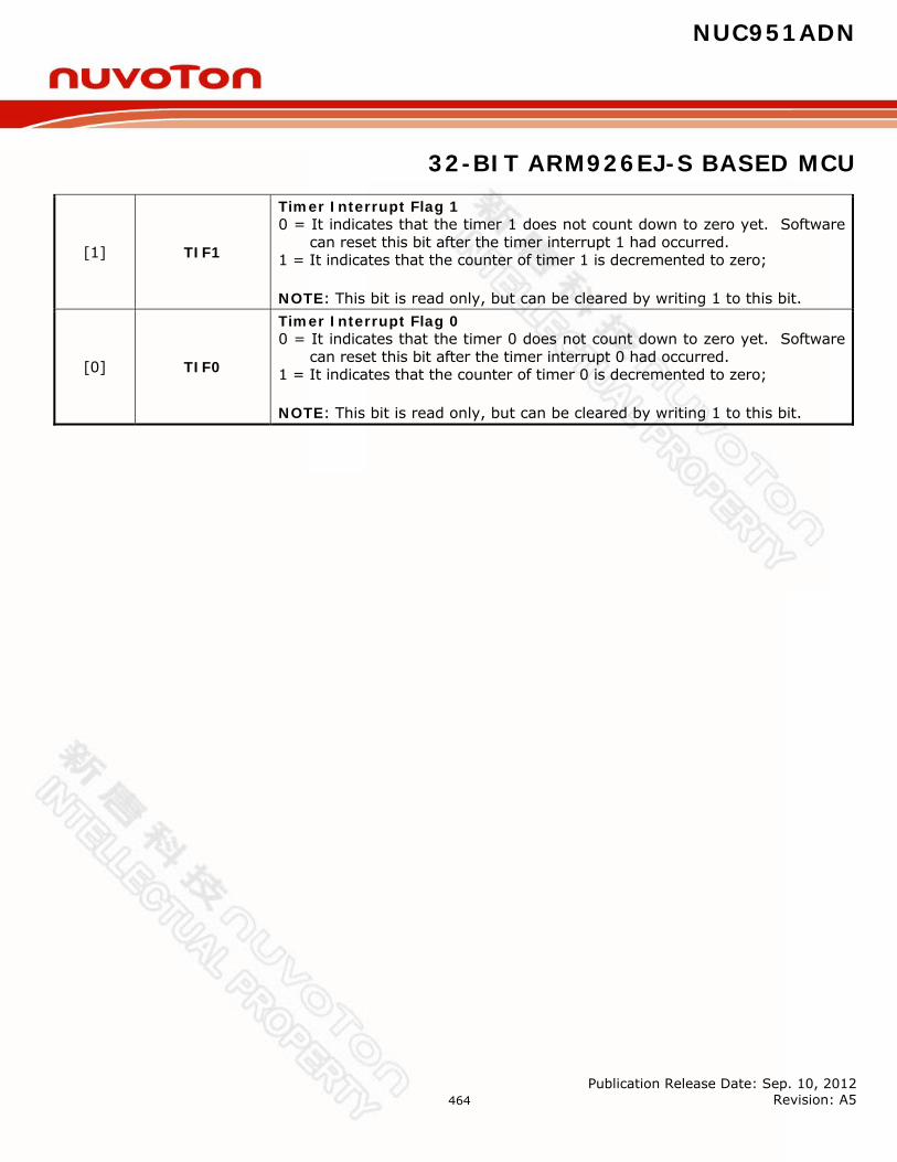
NUC951ADN
32-BIT ARM926EJ-S BASED MCU
Publication Release Date: Sep. 10, 2012 Revision: A5
464
[1] TIF1
Timer Interrupt Flag 1 0 = It indicates that the timer 1 does not count down to zero yet. Software
can reset this bit after the timer interrupt 1 had occurred. 1 = It indicates that the counter of timer 1 is decremented to zero;
NOTE: This bit is read only, but can be cleared by writing 1 to this bit.
[0] TIF0
Timer Interrupt Flag 0 0 = It indicates that the timer 0 does not count down to zero yet. Software
can reset this bit after the timer interrupt 0 had occurred. 1 = It indicates that the counter of timer 0 is decremented to zero;
NOTE: This bit is read only, but can be cleared by writing 1 to this bit.

NUC951ADN
32-BIT ARM926EJ-S BASED MCU
Publication Release Date: Sep. 10, 2012 Revision: A5
465
Watchdog Timer Control Register (WTCR)
Register Address R/W/C Description Reset Value
WTCR 0xB800_101C R/W Watchdog Timer Control Register 0x0000_0000
31 30 29 28 27 26 25 24 RESERVED
23 22 21 20 19 18 17 16 RESERVED
15 14 13 12 11 10 9 8 RESERVED WTCLK RESERVED
7 6 5 4 3 2 1 0 WTE WTIE WTIS WTIF WTRF WTRE WTR
Bits Descriptions
[10] WTCLK
Watchdog Timer Clock This bit is used for deciding whether the Watchdog timer clock input is divided by 256 or not. Clock source of Watchdog timer is Crystal input. 0 = Using original clock input 1 = The clock input will be divided by 256 NOTE: When WTTME = 1, set this bit has no effect on WDT clock (using original clock input).
[7] WTE Watchdog Timer Enable 0 = Disable the watchdog timer 1 = Enable the watchdog timer
[6] WTIE Watchdog Timer Interrupt Enable 0 = Disable the watchdog timer interrupt 1 = Enable the watchdog timer interrupt

NUC951ADN
32-BIT ARM926EJ-S BASED MCU
Publication Release Date: Sep. 10, 2012 Revision: A5
466
[5:4] WTIS
Watchdog Timer Interval Select These two bits select the interval for the watchdog timer. No matter which interval is chosen, the reset time-out is always occurred 1024 clocks later than the interrupt time-out.
WTIS Interrupt Timeout Reset Timeout Real Time Interval
(CLK=15MHz/256) 00 214 clocks 214 + 1024 clocks 0.28 sec. 01 216 clocks 216 + 1024 clocks 1.12 sec. 10 218 clocks 218 + 1024 clocks 4.47 sec. 11 220 clocks 220 + 1024 clocks 17.9 sec.
[3] WTIF
Watchdog Timer Interrupt Flag If the watchdog interrupt is enabled, then the hardware will set this bit to indicate that the watchdog interrupt has occurred. If the watchdog interrupt is not enabled, then this bit indicates that a time-out period has elapsed. 0 = Watchdog timer interrupt does not occur 1 = Watchdog timer interrupt occurs
NOTE: This bit is read only, but can be cleared by writing 1 to this bit.
[2] WTRF
Watchdog Timer Reset Flag When the watchdog timer initiates a reset, the hardware will set this bit. This flag can be read by software to determine the source of reset. Software is responsible to clear it up manually. If WTRE is disabled, then the watchdog timer has no effect on this bit. 0 = Watchdog timer reset does not occur 1 = Watchdog timer reset occurs
[1] WTRE
Watchdog Timer Reset Enable Setting this bit will enable the watchdog timer reset function. 0 = Disable watchdog timer reset function 1 = Enable watchdog timer reset function
NOTE: This bit is read only, but can be cleared by writing 1 to this bit.
[0] WTR
Watchdog Timer Reset This bit brings the watchdog timer into a known state. It helps reset the watchdog timer before a time-out situation occurring. Failing to set WTR before time-out will initiates an interrupt if WTIE is set. If WTRE is set, a watchdog timer reset will be generated 512 clocks after time-out. This bit is self-clearing. 0 = No operation 1 = Reset the contents of the watchdog timer
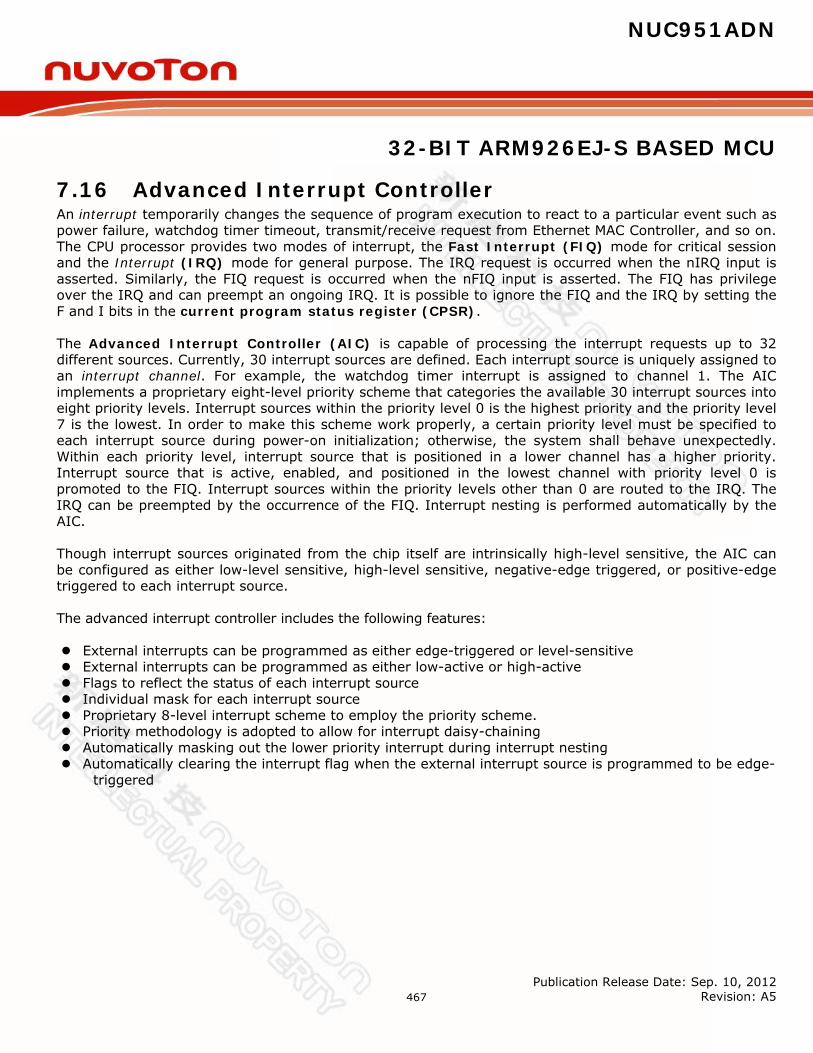
NUC951ADN
32-BIT ARM926EJ-S BASED MCU
Publication Release Date: Sep. 10, 2012 Revision: A5
467
7.16 Advanced Interrupt Controller An interrupt temporarily changes the sequence of program execution to react to a particular event such as power failure, watchdog timer timeout, transmit/receive request from Ethernet MAC Controller, and so on. The CPU processor provides two modes of interrupt, the Fast Interrupt (FIQ) mode for critical session and the Interrupt (IRQ) mode for general purpose. The IRQ request is occurred when the nIRQ input is asserted. Similarly, the FIQ request is occurred when the nFIQ input is asserted. The FIQ has privilege over the IRQ and can preempt an ongoing IRQ. It is possible to ignore the FIQ and the IRQ by setting the F and I bits in the current program status register (CPSR). The Advanced Interrupt Controller (AIC) is capable of processing the interrupt requests up to 32 different sources. Currently, 30 interrupt sources are defined. Each interrupt source is uniquely assigned to an interrupt channel. For example, the watchdog timer interrupt is assigned to channel 1. The AIC implements a proprietary eight-level priority scheme that categories the available 30 interrupt sources into eight priority levels. Interrupt sources within the priority level 0 is the highest priority and the priority level 7 is the lowest. In order to make this scheme work properly, a certain priority level must be specified to each interrupt source during power-on initialization; otherwise, the system shall behave unexpectedly. Within each priority level, interrupt source that is positioned in a lower channel has a higher priority. Interrupt source that is active, enabled, and positioned in the lowest channel with priority level 0 is promoted to the FIQ. Interrupt sources within the priority levels other than 0 are routed to the IRQ. The IRQ can be preempted by the occurrence of the FIQ. Interrupt nesting is performed automatically by the AIC. Though interrupt sources originated from the chip itself are intrinsically high-level sensitive, the AIC can be configured as either low-level sensitive, high-level sensitive, negative-edge triggered, or positive-edge triggered to each interrupt source. The advanced interrupt controller includes the following features: External interrupts can be programmed as either edge-triggered or level-sensitive External interrupts can be programmed as either low-active or high-active Flags to reflect the status of each interrupt source Individual mask for each interrupt source Proprietary 8-level interrupt scheme to employ the priority scheme. Priority methodology is adopted to allow for interrupt daisy-chaining Automatically masking out the lower priority interrupt during interrupt nesting Automatically clearing the interrupt flag when the external interrupt source is programmed to be edge-
triggered
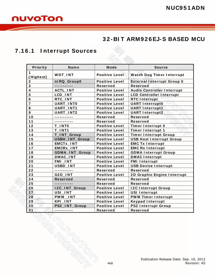
NUC951ADN
32-BIT ARM926EJ-S BASED MCU
Publication Release Date: Sep. 10, 2012 Revision: A5
468
7.16.1 Interrupt Sources
Priority Name Mode Source
1 (Highest) WDT_INT Positive Level Watch Dog Timer Interrupt
2 nIRQ_Group0 Positive Level External Interrupt Group 0 3 ----------- Reserved Reserved 4 ACTL_INT Positive Level Audio Controller Interrupt 5 LCD_INT Positive Level LCD Controller Interrupt 6 RTC_INT Positive Level RTC Interrupt 7 UART_INT0 Positive Level UART Interrupt0 8 UART_INT1 Positive Level UART Interrupt1 9 UART_INT2 Positive Level UART Interrupt2 10 ----------- Reserved Reserved 11 ----------- Reserved Reserved 12 T_INT0 Positive Level Timer Interrupt 0 13 T_INT1 Positive Level Timer Interrupt 1 14 T_INT_Group Positive Level Timer Interrupt Group 15 USBH_INT_Group Positive Level USB Host Interrupt Group 16 EMCTx_INT Positive Level EMC Tx Interrupt 17 EMCRx_INT Positive Level EMC Rx Interrupt 18 GDMA_INT_Group Positive Level GDMA Interrupt Group 19 DMAC_INT Positive Level DMAC Interrupt 20 FMI_INT Positive Level FMI Interrupt 21 USBD_INT Positive Level USB Device Interrupt 22 ----------- Reserved Reserved 23 G2D_INT Positive Level 2D Graphic Engine Interrupt 24 Reserved Reserved Reserved 25 ----------- Reserved Reserved 26 I2C_INT_Group Positive Level I2C Interrupt Group 27 USI_INT Positive Level USI Interrupt 28 PWM _INT Positive Level PWM Timer Interrupt 29 KPI_INT Positive Level Keypad Interrupt 30 PS2_INT_Group Positive Level PS2 Interrupt Group 31 ----------- Reserved Reserved
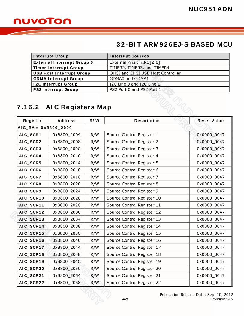
NUC951ADN
32-BIT ARM926EJ-S BASED MCU
Publication Release Date: Sep. 10, 2012 Revision: A5
469
Interrupt Group Interrupt Sources External Interrupt Group 0 External Pins : nIRQ[2:0] Timer Interrupt Group TIMER2, TIMER3, and TIMER4 USB Host Interrupt Group OHCI and EHCI USB Host Controller GDMA Interrupt Group GDMA0 and GDMA1 I2C interrupt Group I2C Line 0 and I2C Line 1 PS2 interrupt Group PS2 Port 0 and PS2 Port 1
7.16.2 AIC Registers Map
Register Address R/W Description Reset Value
AIC_BA = 0xB800_2000
AIC_SCR1 0xB800_2004 R/W Source Control Register 1 0x0000_0047
AIC_SCR2 0xB800_2008 R/W Source Control Register 2 0x0000_0047
AIC_SCR3 0xB800_200C R/W Source Control Register 3 0x0000_0047
AIC_SCR4 0xB800_2010 R/W Source Control Register 4 0x0000_0047
AIC_SCR5 0xB800_2014 R/W Source Control Register 5 0x0000_0047
AIC_SCR6 0xB800_2018 R/W Source Control Register 6 0x0000_0047
AIC_SCR7 0xB800_201C R/W Source Control Register 7 0x0000_0047
AIC_SCR8 0xB800_2020 R/W Source Control Register 8 0x0000_0047
AIC_SCR9 0xB800_2024 R/W Source Control Register 9 0x0000_0047
AIC_SCR10 0xB800_2028 R/W Source Control Register 10 0x0000_0047
AIC_SCR11 0xB800_202C R/W Source Control Register 11 0x0000_0047
AIC_SCR12 0xB800_2030 R/W Source Control Register 12 0x0000_0047
AIC_SCR13 0xB800_2034 R/W Source Control Register 13 0x0000_0047
AIC_SCR14 0xB800_2038 R/W Source Control Register 14 0x0000_0047
AIC_SCR15 0xB800_203C R/W Source Control Register 15 0x0000_0047
AIC_SCR16 0xB800_2040 R/W Source Control Register 16 0x0000_0047
AIC_SCR17 0xB800_2044 R/W Source Control Register 17 0x0000_0047
AIC_SCR18 0xB800_2048 R/W Source Control Register 18 0x0000_0047
AIC_SCR19 0xB800_204C R/W Source Control Register 19 0x0000_0047
AIC_SCR20 0xB800_2050 R/W Source Control Register 20 0x0000_0047
AIC_SCR21 0xB800_2054 R/W Source Control Register 21 0x0000_0047
AIC_SCR22 0xB800_2058 R/W Source Control Register 22 0x0000_0047

NUC951ADN
32-BIT ARM926EJ-S BASED MCU
Publication Release Date: Sep. 10, 2012 Revision: A5
470
AIC_SCR23 0xB800_205C R/W Source Control Register 23 0x0000_0047
AIC_SCR24 0xB800_2060 R/W Reserved 0x0000_0047
AIC_SCR25 0xB800_2064 R/W Source Control Register 25 0x0000_0047
AIC_SCR26 0xB800_2068 R/W Source Control Register 26 0x0000_0047
AIC_SCR27 0xB800_206C R/W Source Control Register 27 0x0000_0047
AIC_SCR28 0xB800_2070 R/W Source Control Register 28 0x0000_0047
AIC_SCR29 0xB800_2074 R/W Source Control Register 29 0x0000_0047
AIC_SCR30 0xB800_2078 R/W Source Control Register 30 0x0000_0047
AIC_SCR31 0xB800_207C R/W Source Control Register 31 0x0000_0047
AIC_IRQSC 0xB800_2080 R/W External Interrupt Control Register 0x0000_0000
AIC_GEN 0xB800_2084 R/W Interrupt Group Enable Control Register 0x0000_0000
AIC_GASR 0xB800_2088 R Interrupt Group Active Status Register 0x0000_0000
AIC_GSCR 0xB800_208C W/R Interrupt Group Status Clear Register 0x0000_0000
AIC_IRSR 0xB800_2100 R Interrupt Raw Status Register 0x0000_0000
AIC_IASR 0xB800_2104 R Interrupt Active Status Register 0x0000_0000
AIC_ISR 0xB800_2108 R Interrupt Status Register 0x0000_0000
AIC_IPER 0xB800_210C R Interrupt Priority Encoding Register 0x0000_0000
AIC_ISNR 0xB800_2110 R Interrupt Source Number Register 0x0000_0000
AIC_IMR 0xB800_2114 R Interrupt Mask Register 0x0000_0000
AIC_OISR 0xB800_2118 R Output Interrupt Status Register 0x0000_0000
AIC_MECR 0xB800_2120 W Mask Enable Command Register Undefined
AIC_MDCR 0xB800_2124 W Mask Disable Command Register Undefined AIC_EOSCR 0xB800_2130 W End of Service Command Register Undefined
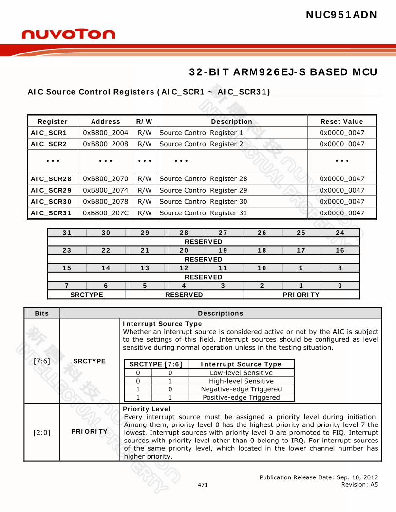
NUC951ADN
32-BIT ARM926EJ-S BASED MCU
Publication Release Date: Sep. 10, 2012 Revision: A5
471
AIC Source Control Registers (AIC_SCR1 ~ AIC_SCR31)
Register Address R/W Description Reset Value
AIC_SCR1 0xB800_2004 R/W Source Control Register 1 0x0000_0047
AIC_SCR2 0xB800_2008 R/W Source Control Register 2 0x0000_0047
AIC_SCR28 0xB800_2070 R/W Source Control Register 28 0x0000_0047
AIC_SCR29 0xB800_2074 R/W Source Control Register 29 0x0000_0047
AIC_SCR30 0xB800_2078 R/W Source Control Register 30 0x0000_0047
AIC_SCR31 0xB800_207C R/W Source Control Register 31 0x0000_0047
31 30 29 28 27 26 25 24 RESERVED
23 22 21 20 19 18 17 16 RESERVED
15 14 13 12 11 10 9 8 RESERVED
7 6 5 4 3 2 1 0 SRCTYPE RESERVED PRIORITY
Bits Descriptions
[7:6] SRCTYPE
Interrupt Source Type Whether an interrupt source is considered active or not by the AIC is subject to the settings of this field. Interrupt sources should be configured as level sensitive during normal operation unless in the testing situation.
SRCTYPE [7:6] Interrupt Source Type 0 0 Low-level Sensitive 0 1 High-level Sensitive 1 0 Negative-edge Triggered 1 1 Positive-edge Triggered
[2:0] PRIORITY
Priority Level Every interrupt source must be assigned a priority level during initiation. Among them, priority level 0 has the highest priority and priority level 7 the lowest. Interrupt sources with priority level 0 are promoted to FIQ. Interrupt sources with priority level other than 0 belong to IRQ. For interrupt sources of the same priority level, which located in the lower channel number has higher priority.
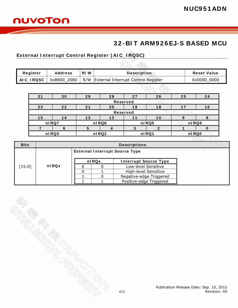
NUC951ADN
32-BIT ARM926EJ-S BASED MCU
Publication Release Date: Sep. 10, 2012 Revision: A5
472
External Interrupt Control Register (AIC_IRQSC)
Register Address R/W Description Reset Value
AIC_IRQSC 0xB800_2080 R/W External Interrupt Control Register 0x0000_0000
31 30 29 28 27 26 25 24 Reserved
23 22 21 20 19 18 17 16 Reserved
15 14 13 12 11 10 9 8 nIRQ7 nIRQ6 nIRQ5 nIRQ4
7 6 5 4 3 2 1 0 nIRQ3 nIRQ2 nIRQ1 nIRQ0
Bits Descriptions
[15:0] nIRQ x
External Interrupt Source Type
nIRQx Interrupt Source Type 0 0 Low-level Sensitive 0 1 High-level Sensitive 1 0 Negative-edge Triggered 1 1 Positive-edge Triggered
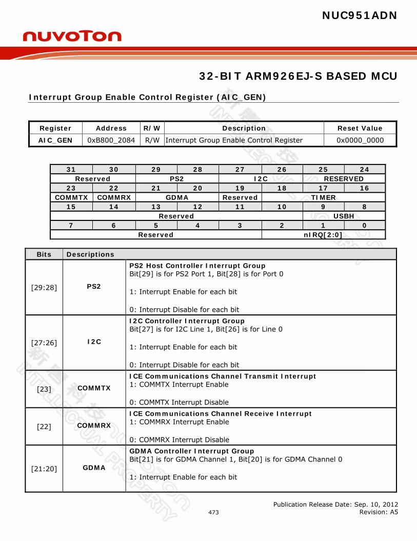
NUC951ADN
32-BIT ARM926EJ-S BASED MCU
Publication Release Date: Sep. 10, 2012 Revision: A5
473
Interrupt Group Enable Control Register (AIC_GEN)
Register Address R/W Description Reset Value
AIC_GEN 0xB800_2084 R/W Interrupt Group Enable Control Register 0x0000_0000
31 30 29 28 27 26 25 24 Reserved PS2 I2C RESERVED
23 22 21 20 19 18 17 16 COMMTX COMMRX GDMA Reserved TIMER
15 14 13 12 11 10 9 8 Reserved USBH
7 6 5 4 3 2 1 0 Reserved nIRQ[2:0]
Bits Descriptions
[29:28] PS2
PS2 Host Controller Interrupt Group Bit[29] is for PS2 Port 1, Bit[28] is for Port 0
1: Interrupt Enable for each bit
0: Interrupt Disable for each bit
[27:26] I2C
I2C Controller Interrupt Group Bit[27] is for I2C Line 1, Bit[26] is for Line 0
1: Interrupt Enable for each bit
0: Interrupt Disable for each bit
[23] COMMTX
ICE Communications Channel Transmit Interrupt 1: COMMTX Interrupt Enable
0: COMMTX Interrupt Disable
[22] COMMRX
ICE Communications Channel Receive Interrupt 1: COMMRX Interrupt Enable
0: COMMRX Interrupt Disable
[21:20] GDMA
GDMA Controller Interrupt Group Bit[21] is for GDMA Channel 1, Bit[20] is for GDMA Channel 0
1: Interrupt Enable for each bit
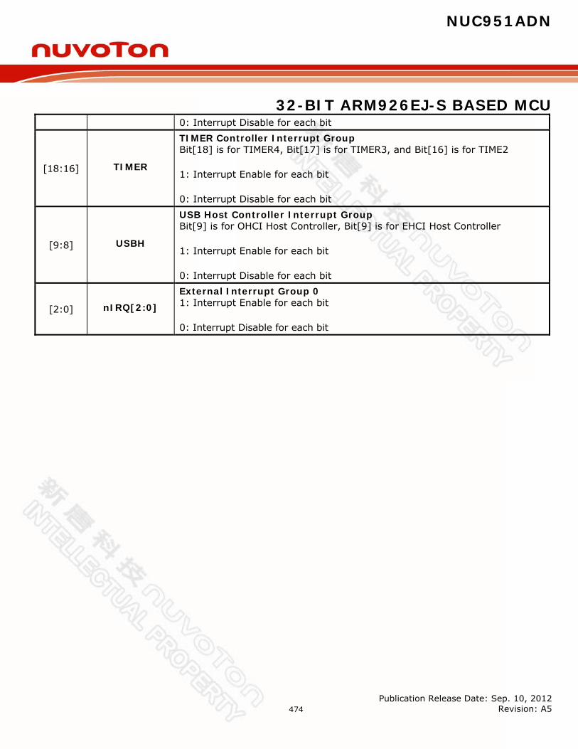
NUC951ADN
32-BIT ARM926EJ-S BASED MCU
Publication Release Date: Sep. 10, 2012 Revision: A5
474
0: Interrupt Disable for each bit
[18:16] TIMER
TIMER Controller Interrupt Group Bit[18] is for TIMER4, Bit[17] is for TIMER3, and Bit[16] is for TIME2
1: Interrupt Enable for each bit
0: Interrupt Disable for each bit
[9:8] USBH
USB Host Controller Interrupt Group Bit[9] is for OHCI Host Controller, Bit[9] is for EHCI Host Controller
1: Interrupt Enable for each bit
0: Interrupt Disable for each bit
[2:0] nIRQ[2:0]
External Interrupt Group 0 1: Interrupt Enable for each bit
0: Interrupt Disable for each bit
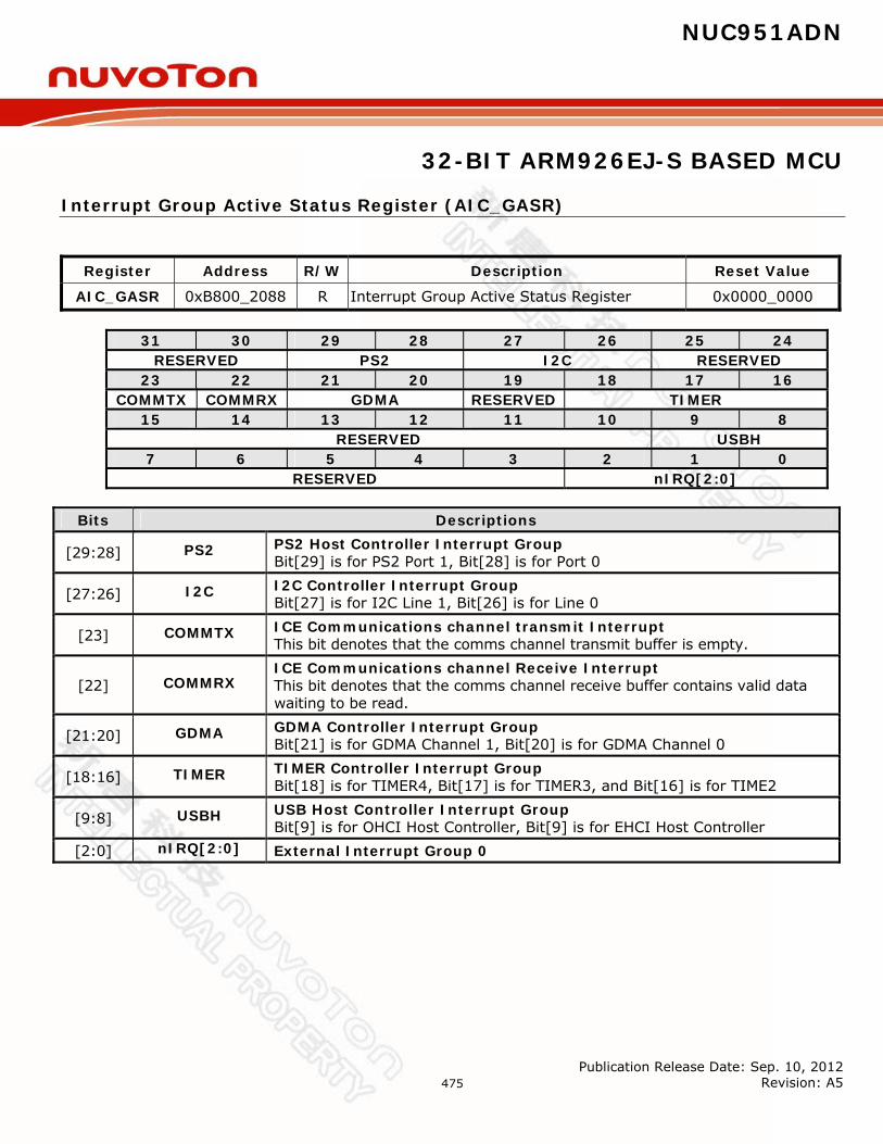
NUC951ADN
32-BIT ARM926EJ-S BASED MCU
Publication Release Date: Sep. 10, 2012 Revision: A5
475
Interrupt Group Active Status Register (AIC_GASR)
Register Address R/W Description Reset Value
AIC_GASR 0xB800_2088 R Interrupt Group Active Status Register 0x0000_0000
31 30 29 28 27 26 25 24 RESERVED PS2 I2C RESERVED
23 22 21 20 19 18 17 16 COMMTX COMMRX GDMA RESERVED TIMER
15 14 13 12 11 10 9 8 RESERVED USBH
7 6 5 4 3 2 1 0 RESERVED nIRQ[2:0]
Bits Descriptions
[29:28] PS2 PS2 Host Controller Interrupt Group Bit[29] is for PS2 Port 1, Bit[28] is for Port 0
[27:26] I2C I2C Controller Interrupt Group Bit[27] is for I2C Line 1, Bit[26] is for Line 0
[23] COMMTX ICE Communications channel transmit Interrupt This bit denotes that the comms channel transmit buffer is empty.
[22] COMMRX ICE Communications channel Receive Interrupt This bit denotes that the comms channel receive buffer contains valid data waiting to be read.
[21:20] GDMA GDMA Controller Interrupt Group Bit[21] is for GDMA Channel 1, Bit[20] is for GDMA Channel 0
[18:16] TIMER TIMER Controller Interrupt Group Bit[18] is for TIMER4, Bit[17] is for TIMER3, and Bit[16] is for TIME2
[9:8] USBH USB Host Controller Interrupt Group Bit[9] is for OHCI Host Controller, Bit[9] is for EHCI Host Controller
[2:0] nIRQ[2:0] External Interrupt Group 0

NUC951ADN
32-BIT ARM926EJ-S BASED MCU
Publication Release Date: Sep. 10, 2012 Revision: A5
476
Interrupt Group Status Clear Register (AIC_GSCR)
Register Address R/W Description Reset Value
AIC_GSCR 0xB800_208C R/W Interrupt Group Status Clear Register 0x0000_0000
31 30 29 28 27 26 25 24 Reserved
23 22 21 20 19 18 17 16 Reserved
15 14 13 12 11 10 9 8 Reserved
7 6 5 4 3 2 1 0 Reserved nIRQ[2:0]
Bits Descriptions
[2:0] nIRQ[2:0] External Interrupt Group 0 Write 1: Clear the relative status bit, and this bit is auto clear to 0 Write 0: No action
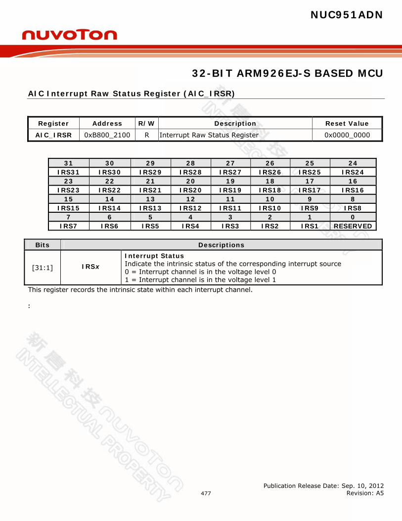
NUC951ADN
32-BIT ARM926EJ-S BASED MCU
Publication Release Date: Sep. 10, 2012 Revision: A5
477
AIC Interrupt Raw Status Register (AIC_IRSR)
Register Address R/W Description Reset Value
AIC_IRSR 0xB800_2100 R Interrupt Raw Status Register 0x0000_0000
31 30 29 28 27 26 25 24 IRS31 IRS30 IRS29 IRS28 IRS27 IRS26 IRS25 IRS24
23 22 21 20 19 18 17 16 IRS23 IRS22 IRS21 IRS20 IRS19 IRS18 IRS17 IRS16
15 14 13 12 11 10 9 8 IRS15 IRS14 IRS13 IRS12 IRS11 IRS10 IRS9 IRS8
7 6 5 4 3 2 1 0 IRS7 IRS6 IRS5 IRS4 IRS3 IRS2 IRS1 RESERVED
Bits Descriptions
[31:1] IRS x Interrupt Status Indicate the intrinsic status of the corresponding interrupt source 0 = Interrupt channel is in the voltage level 0 1 = Interrupt channel is in the voltage level 1
This register records the intrinsic state within each interrupt channel. :
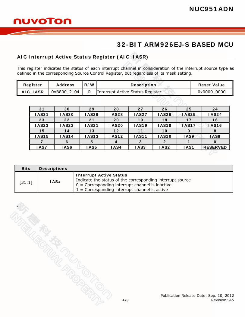
NUC951ADN
32-BIT ARM926EJ-S BASED MCU
Publication Release Date: Sep. 10, 2012 Revision: A5
478
AIC Interrupt Active Status Register (AIC_IASR)
This register indicates the status of each interrupt channel in consideration of the interrupt source type as defined in the corresponding Source Control Register, but regardless of its mask setting.
Register Address R/W Description Reset Value
AIC_IASR 0xB800_2104 R Interrupt Active Status Register 0x0000_0000
31 30 29 28 27 26 25 24 IAS31 IAS30 IAS29 IAS28 IAS27 IAS26 IAS25 IAS24
23 22 21 20 19 18 17 16 IAS23 IAS22 IAS21 IAS20 IAS19 IAS18 IAS17 IAS16
15 14 13 12 11 10 9 8 IAS15 IAS14 IAS13 IAS12 IAS11 IAS10 IAS9 IAS8
7 6 5 4 3 2 1 0 IAS7 IAS6 IAS5 IAS4 IAS3 IAS2 IAS1 RESERVED
Bits Descriptions
[31:1] IAS x Interrupt Active Status Indicate the status of the corresponding interrupt source 0 = Corresponding interrupt channel is inactive 1 = Corresponding interrupt channel is active
:

NUC951ADN
32-BIT ARM926EJ-S BASED MCU
Publication Release Date: Sep. 10, 2012 Revision: A5
479
AIC Interrupt Status Register (AIC_ISR)
This register identifies those interrupt channels whose are both active and enabled.
Register Address R/W Description Reset Value
AIC_ISR 0xB800_2108 R Interrupt Status Register 0x0000_0000
31 30 29 28 27 26 25 24 IS31 IS30 IS29 IS28 IS27 IS26 IS25 IS24 23 22 21 20 19 18 17 16
IS23 IS22 IS21 IS20 IS19 IS18 IS17 IS16 15 14 13 12 11 10 9 8
IS15 IS14 IS13 IS12 IS11 IS10 IS9 IS8 7 6 5 4 3 2 1 0
IS7 IS6 IS5 IS4 IS3 IS2 IS1 RESERVED
Bits Descriptions
[31:1] IS x
Interrupt Status Indicates the status of corresponding interrupt channel 0 = Two possibilities:
(1) The corresponding interrupt channel is inactive no matter whether it is enabled or disabled;
(2) It is active but not enabled 1 = Corresponding interrupt channel is both active and enabled (can assert
an interrupt)
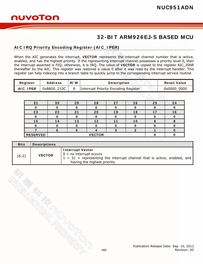
NUC951ADN
32-BIT ARM926EJ-S BASED MCU
Publication Release Date: Sep. 10, 2012 Revision: A5
480
AIC IRQ Priority Encoding Register (AIC_IPER)
When the AIC generates the interrupt, VECTOR represents the interrupt channel number that is active, enabled, and has the highest priority. If the representing interrupt channel possesses a priority level 0, then the interrupt asserted is FIQ; otherwise, it is IRQ. The value of VECTOR is copied to the register AIC_ISNR thereafter by the AIC. This register was restored a value 0 after it was read by the interrupt handler. This register can help indexing into a branch table to quickly jump to the corresponding interrupt service routine.
Register Address R/W Description Reset Value
AIC_IPER 0xB800_210C R Interrupt Priority Encoding Register 0x0000_0000
31 30 29 28 27 26 25 24 0 0 0 0 0 0 0 0
23 22 21 20 19 18 17 16 0 0 0 0 0 0 0 0
15 14 13 12 11 10 9 8 0 0 0 0 0 0 0 0 7 6 5 4 3 2 1 0
RESERVED VECTOR 0 0
Bits Descriptions
[6:2] VECTOR Interrupt Vector 0 = no interrupt occurs 1 ~ 31 = representing the interrupt channel that is active, enabled, and
having the highest priority
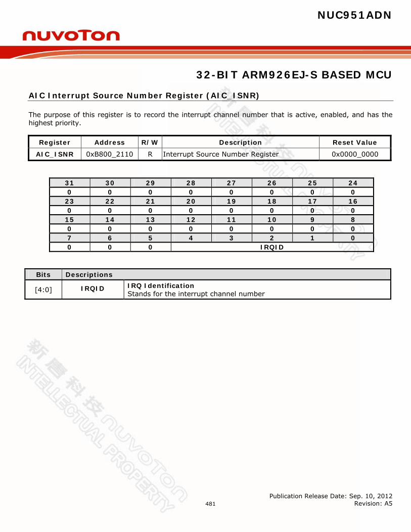
NUC951ADN
32-BIT ARM926EJ-S BASED MCU
Publication Release Date: Sep. 10, 2012 Revision: A5
481
AIC Interrupt Source Number Register (AIC_ISNR)
The purpose of this register is to record the interrupt channel number that is active, enabled, and has the highest priority.
Register Address R/W Description Reset Value
AIC_ISNR 0xB800_2110 R Interrupt Source Number Register 0x0000_0000
31 30 29 28 27 26 25 24 0 0 0 0 0 0 0 0
23 22 21 20 19 18 17 16 0 0 0 0 0 0 0 0
15 14 13 12 11 10 9 8 0 0 0 0 0 0 0 0 7 6 5 4 3 2 1 0 0 0 0 IRQID
Bits Descriptions
[4:0] IRQID IRQ Identification Stands for the interrupt channel number

NUC951ADN
32-BIT ARM926EJ-S BASED MCU
Publication Release Date: Sep. 10, 2012 Revision: A5
482
AIC Interrupt Mask Register (AIC_IMR)
Register Address R/W Description Reset Value
AIC_IMR 0xB800_2114 R Interrupt Mask Register 0x0000_0000
31 30 29 28 27 26 25 24 IM31 IM30 IM29 IM28 IM27 IM26 IM25 IM24
23 22 21 20 19 18 17 16 IM23 IM22 IM21 IM20 IM19 IM18 IM17 IM16
15 14 13 12 11 10 9 8 IM15 IM14 IM13 IM12 IM11 IM10 IM9 IM8
7 6 5 4 3 2 1 0 IM7 IM6 IM5 IM4 IM3 IM2 IM1 RESERVED
Bits Descriptions
[31:1] IM x
Interrupt Mask This bit determines whether the corresponding interrupt channel is enabled or disabled. Every interrupt channel can be active no matter whether it is enabled or disabled. If an interrupt channel is enabled, it does not definitely mean it is active. Every interrupt channel can be authorized by the AIC only when it is both active and enabled. 0 = Corresponding interrupt channel is disabled 1 = Corresponding interrupt channel is enabled
:
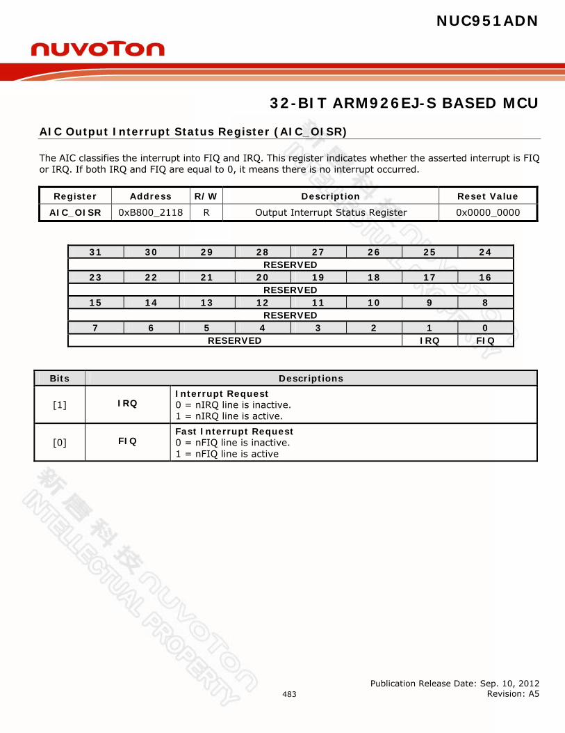
NUC951ADN
32-BIT ARM926EJ-S BASED MCU
Publication Release Date: Sep. 10, 2012 Revision: A5
483
AIC Output Interrupt Status Register (AIC_OISR)
The AIC classifies the interrupt into FIQ and IRQ. This register indicates whether the asserted interrupt is FIQ or IRQ. If both IRQ and FIQ are equal to 0, it means there is no interrupt occurred.
Register Address R/W Description Reset Value
AIC_OISR 0xB800_2118 R Output Interrupt Status Register 0x0000_0000
31 30 29 28 27 26 25 24 RESERVED
23 22 21 20 19 18 17 16 RESERVED
15 14 13 12 11 10 9 8 RESERVED
7 6 5 4 3 2 1 0 RESERVED IRQ FIQ
Bits Descriptions
[1] IRQ Interrupt Request 0 = nIRQ line is inactive. 1 = nIRQ line is active.
[0] FIQ Fast Interrupt Request 0 = nFIQ line is inactive. 1 = nFIQ line is active
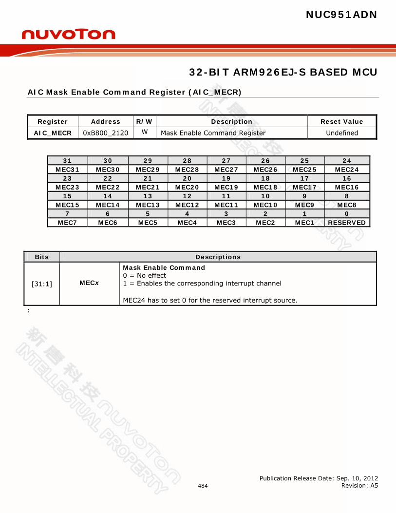
NUC951ADN
32-BIT ARM926EJ-S BASED MCU
Publication Release Date: Sep. 10, 2012 Revision: A5
484
AIC Mask Enable Command Register (AIC_MECR)
Register Address R/W Description Reset Value
AIC_MECR 0xB800_2120 W Mask Enable Command Register Undefined
31 30 29 28 27 26 25 24 MEC31 MEC30 MEC29 MEC28 MEC27 MEC26 MEC25 MEC24
23 22 21 20 19 18 17 16 MEC23 MEC22 MEC21 MEC20 MEC19 MEC18 MEC17 MEC16
15 14 13 12 11 10 9 8 MEC15 MEC14 MEC13 MEC12 MEC11 MEC10 MEC9 MEC8
7 6 5 4 3 2 1 0 MEC7 MEC6 MEC5 MEC4 MEC3 MEC2 MEC1 RESERVED
Bits Descriptions
[31:1] MEC x
Mask Enable Command 0 = No effect 1 = Enables the corresponding interrupt channel
MEC24 has to set 0 for the reserved interrupt source. :
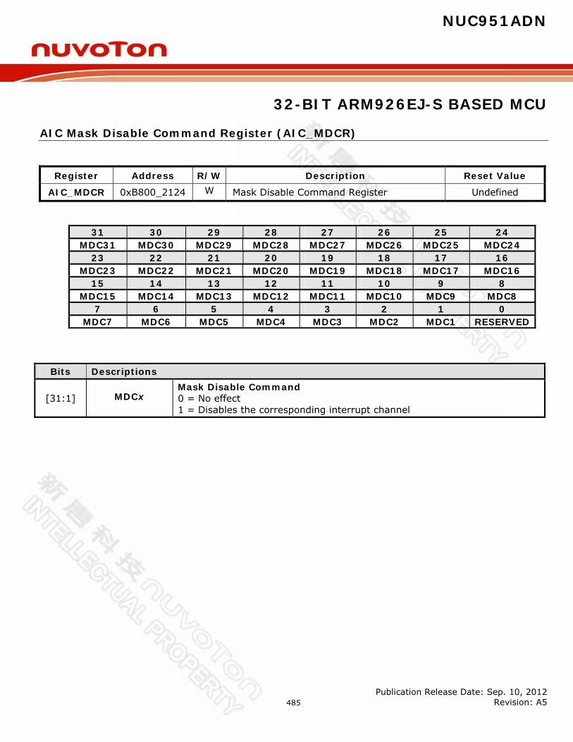
NUC951ADN
32-BIT ARM926EJ-S BASED MCU
Publication Release Date: Sep. 10, 2012 Revision: A5
485
AIC Mask Disable Command Register (AIC_MDCR)
Register Address R/W Description Reset Value
AIC_MDCR 0xB800_2124 W Mask Disable Command Register Undefined
31 30 29 28 27 26 25 24 MDC31 MDC30 MDC29 MDC28 MDC27 MDC26 MDC25 MDC24
23 22 21 20 19 18 17 16 MDC23 MDC22 MDC21 MDC20 MDC19 MDC18 MDC17 MDC16
15 14 13 12 11 10 9 8 MDC15 MDC14 MDC13 MDC12 MDC11 MDC10 MDC9 MDC8
7 6 5 4 3 2 1 0 MDC7 MDC6 MDC5 MDC4 MDC3 MDC2 MDC1 RESERVED
Bits Descriptions
[31:1] MDC x Mask Disable Command 0 = No effect 1 = Disables the corresponding interrupt channel
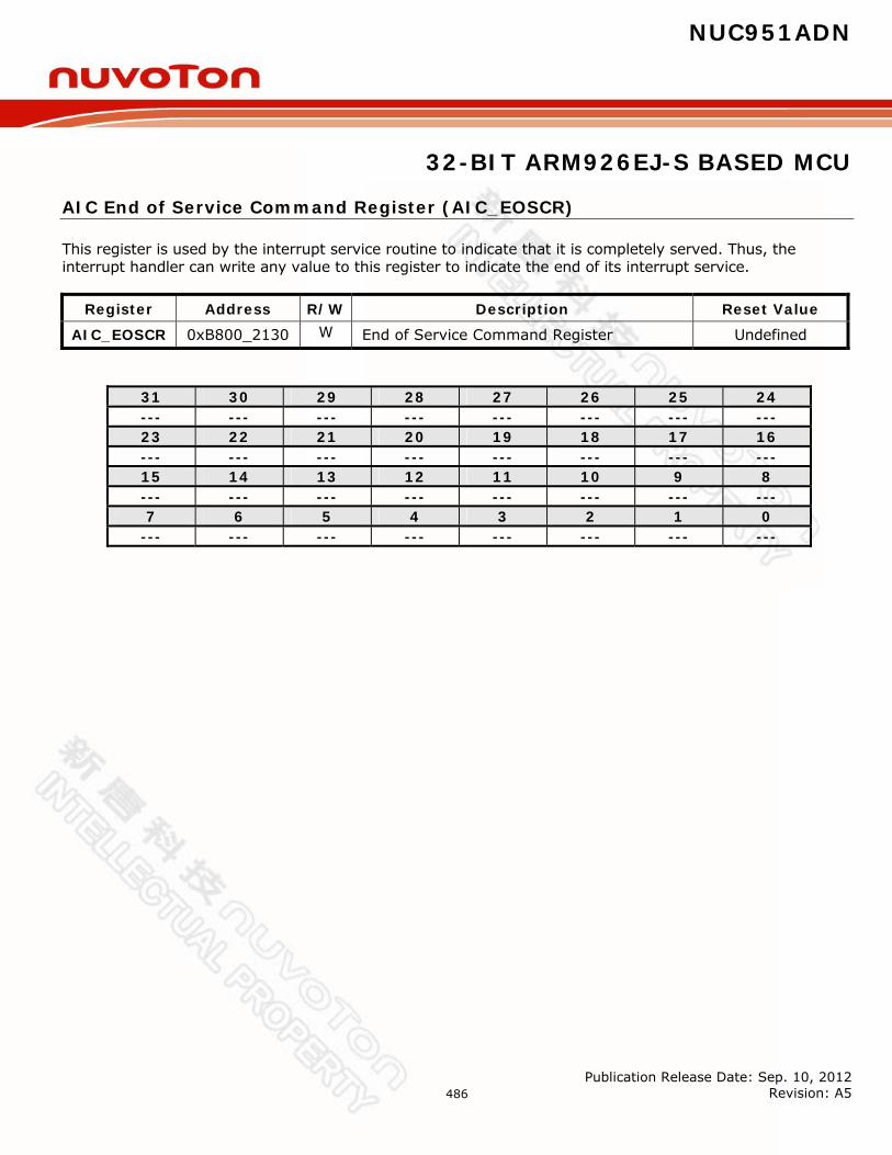
NUC951ADN
32-BIT ARM926EJ-S BASED MCU
Publication Release Date: Sep. 10, 2012 Revision: A5
486
AIC End of Service Command Register (AIC_EOSCR)
This register is used by the interrupt service routine to indicate that it is completely served. Thus, the interrupt handler can write any value to this register to indicate the end of its interrupt service.
Register Address R/W Description Reset Value
AIC_EOSCR 0xB800_2130 W End of Service Command Register Undefined
31 30 29 28 27 26 25 24 --- --- --- --- --- --- --- --- 23 22 21 20 19 18 17 16 --- --- --- --- --- --- --- --- 15 14 13 12 11 10 9 8 --- --- --- --- --- --- --- --- 7 6 5 4 3 2 1 0
--- --- --- --- --- --- --- ---
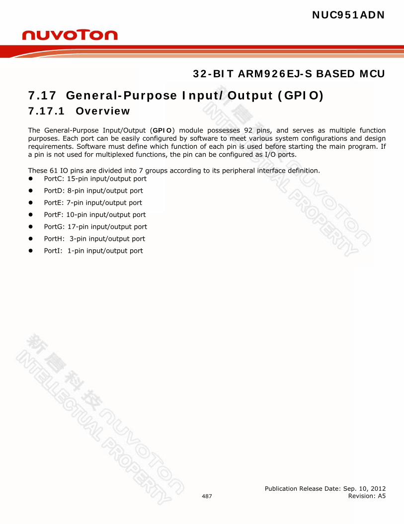
NUC951ADN
32-BIT ARM926EJ-S BASED MCU
Publication Release Date: Sep. 10, 2012 Revision: A5
487
7.17 General-Purpose Input/Output (GPIO) 7.17.1 Overview The General-Purpose Input/Output (GPIO) module possesses 92 pins, and serves as multiple function purposes. Each port can be easily configured by software to meet various system configurations and design requirements. Software must define which function of each pin is used before starting the main program. If a pin is not used for multiplexed functions, the pin can be configured as I/O ports. These 61 IO pins are divided into 7 groups according to its peripheral interface definition. PortC: 15-pin input/output port
PortD: 8-pin input/output port
PortE: 7-pin input/output port
PortF: 10-pin input/output port
PortG: 17-pin input/output port
PortH: 3-pin input/output port
PortI: 1-pin input/output port
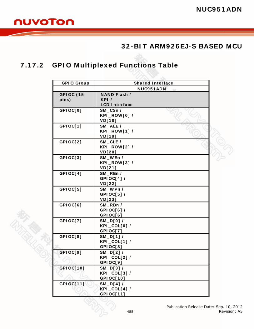
NUC951ADN
32-BIT ARM926EJ-S BASED MCU
Publication Release Date: Sep. 10, 2012 Revision: A5
488
7.17.2 GPIO Multiplexed Functions Table
GPIO Group Shared Interface NUC951ADN GPIOC (15 pins)
NAND Flash / KPI / LCD Interface
GPIOC[0] SM_CSn / KPI_ROW[0] / VD[18]
GPIOC[1] SM_ALE / KPI_ROW[1] / VD[19]
GPIOC[2] SM_CLE / KPI_ROW[2] / VD[20]
GPIOC[3] SM_WEn / KPI_ROW[3] / VD[21]
GPIOC[4] SM_REn / GPIOC[4] / VD[22]
GPIOC[5] SM_WPn / GPIOC[5] / VD[23]
GPIOC[6] SM_RBn / GPIOC[6] / GPIOC[6]
GPIOC[7] SM_D[0] / KPI_COL[0] / GPIOC[7]
GPIOC[8] SM_D[1] / KPI_COL[1] / GPIOC[8]
GPIOC[9] SM_D[2] / KPI_COL[2] / GPIOC[9]
GPIOC[10] SM_D[3] / KPI_COL[3] / GPIOC[10]
GPIOC[11] SM_D[4] / KPI_COL[4] / GPIOC[11]
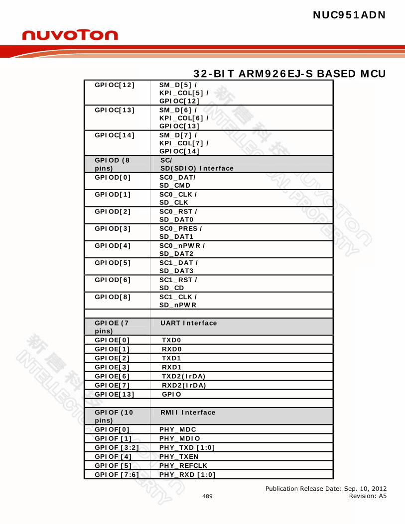
NUC951ADN
32-BIT ARM926EJ-S BASED MCU
Publication Release Date: Sep. 10, 2012 Revision: A5
489
GPIOC[12] SM_D[5] / KPI_COL[5] / GPIOC[12]
GPIOC[13] SM_D[6] / KPI_COL[6] / GPIOC[13]
GPIOC[14] SM_D[7] / KPI_COL[7] / GPIOC[14]
GPIOD (8 pins)
SC/ SD(SDIO) Interface
GPIOD[0] SC0_DAT/ SD_CMD
GPIOD[1] SC0_CLK / SD_CLK
GPIOD[2] SC0_RST / SD_DAT0
GPIOD[3] SC0_PRES / SD_DAT1
GPIOD[4] SC0_nPWR / SD_DAT2
GPIOD[5] SC1_DAT / SD_DAT3
GPIOD[6] SC1_RST / SD_CD
GPIOD[8] SC1_CLK / SD_nPWR
GPIOE (7 pins)
UART Interface
GPIOE[0] TXD0 GPIOE[1] RXD0 GPIOE[2] TXD1 GPIOE[3] RXD1 GPIOE[6] TXD2(IrDA) GPIOE[7] RXD2(IrDA) GPIOE[13] GPIO GPIOF (10 pins)
RMII Interface
GPIOF[0] PHY_MDC GPIOF [1] PHY_MDIO GPIOF [3:2] PHY_TXD [1:0] GPIOF [4] PHY_TXEN GPIOF [5] PHY_REFCLK GPIOF [7:6] PHY_RXD [1:0]
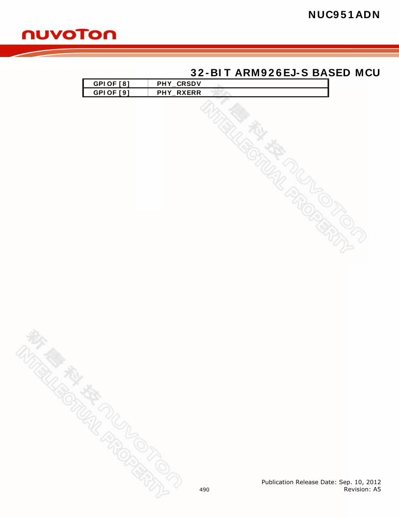
NUC951ADN
32-BIT ARM926EJ-S BASED MCU
Publication Release Date: Sep. 10, 2012 Revision: A5
490
GPIOF [8] PHY_CRSDV GPIOF [9] PHY_RXERR
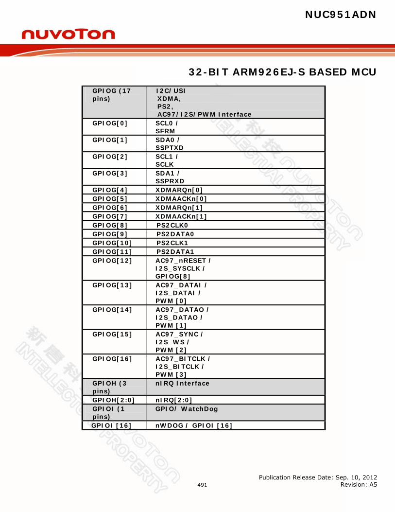
NUC951ADN
32-BIT ARM926EJ-S BASED MCU
Publication Release Date: Sep. 10, 2012 Revision: A5
491
GPIOG (17 pins)
I2C/USI XDMA, PS2, AC97/I2S/PWM Interface
GPIOG[0] SCL0 / SFRM
GPIOG[1] SDA0 / SSPTXD
GPIOG[2] SCL1 / SCLK
GPIOG[3] SDA1 / SSPRXD
GPIOG[4] XDMARQn[0] GPIOG[5] XDMAACKn[0] GPIOG[6] XDMARQn[1] GPIOG[7] XDMAACKn[1] GPIOG[8] PS2CLK0 GPIOG[9] PS2DATA0 GPIOG[10] PS2CLK1 GPIOG[11] PS2DATA1 GPIOG[12] AC97_nRESET /
I2S_SYSCLK / GPIOG[8]
GPIOG[13] AC97_DATAI / I2S_DATAI / PWM [0]
GPIOG[14] AC97_DATAO / I2S_DATAO / PWM [1]
GPIOG[15] AC97_SYNC / I2S_WS / PWM [2]
GPIOG[16] AC97_BITCLK / I2S_BITCLK / PWM [3]
GPIOH (3 pins)
nIRQ Interface
GPIOH[2:0] nIRQ[2:0] GPIOI (1 pins)
GPIO/ WatchDog
GPIOI [16] nWDOG / GPIOI [16]

NUC951ADN
32-BIT ARM926EJ-S BASED MCU
Publication Release Date: Sep. 10, 2012 Revision: A5
492
7.17.3 GPIO Control Registers Map
Register Address R/W Description Reset Value GPIO_BA = 0xB800_3000 GPIOC_DIR 0xB800_3004 R/W GPIO portC direction control register 0x0000_0000 GPIOC_DATAOUT 0xB800_3008 R/W GPIO portC data output register 0x0000_0000 GPIOC_DATAIN 0xB800_300C R GPIO portC data input register Undefined GPIOD_DIR 0xB800_3014 R/W GPIO portD direction control register 0x0000_0000 GPIOD_DATAOUT 0xB800_3018 R/W GPIO portD data output register 0x0000_0000 GPIOD_DATAIN 0xB800_301C R GPIO portD data input register Undefined GPIOE_DIR 0xB800_3024 R/W GPIO portE direction control register 0x0000_0000 GPIOE_DATAOUT 0xB800_3028 R/W GPIO portE data output register 0x0000_0000 GPIOE_DATAIN 0xB800_302C R GPIO portE data input register 0x0000_0000 GPIOF_DIR 0xB800_3034 R/W GPIO portF direction control register 0x0000_0000 GPIOF_DATAOUT 0xB800_3038 R/W GPIO portF data output register 0x0000_0000 GPIOF_DATAIN 0xB800_303C R GPIO portF data input register Undefined GPIOG_DIR 0xB800_3044 R/W GPIO portG direction control register 0x0000_0000 GPIOG_DATAOUT 0xB800_3048 R/W GPIO portG data output register 0x0000_0000 GPIOG_DATAIN 0xB800_304C R GPIO portG data input register Undefined GPIOH_DBNCE 0xB800_3050 R/W GPIO portH input de-bounce control
reg. 0x0000_0000
GPIOH_DIR 0xB800_3054 R/W GPIO portH direction control register 0x0000_0000 GPIOH_DATAOUT 0xB800_3058 R/W GPIO portH data output register 0x0000_0000 GPIOH_DATAIN 0xB800_305C R GPIO portH data input register Undefined GPIOI_DIR 0xB800_3064 R/W GPIO portI direction control register 0x0000_0000 GPIOI_DATAOUT 0xB800_3068 R/W GPIO portI data output register 0x0000_0000 GPIOI_DATAIN 0xB800_306C R GPIO portI data input register Undefined
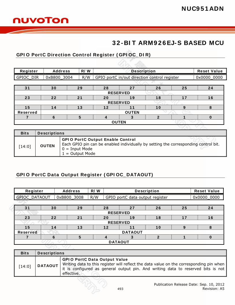
NUC951ADN
32-BIT ARM926EJ-S BASED MCU
Publication Release Date: Sep. 10, 2012 Revision: A5
493
GPIO PortC Direction Control Register (GPIOC_DIR)
Register Address R/W Description Reset Value
GPIOC_DIR 0xB800_3004 R/W GPIO portC in/out direction control register 0x0000_0000
31 30 29 28 27 26 25 24 RESERVED
23 22 21 20 19 18 17 16 RESERVED
15 14 13 12 11 10 9 8 Reserved OUTEN
7 6 5 4 3 2 1 0 OUTEN
Bits Descriptions
[14:0] OUTEN GPIO PortC Output Enable Control Each GPIO pin can be enabled individually by setting the corresponding control bit. 0 = Input Mode 1 = Output Mode
GPIO PortC Data Output Register (GPIOC_DATAOUT)
Register Address R/W Description Reset Value
GPIOC_DATAOUT 0xB800_3008 R/W GPIO portC data output register 0x0000_0000
31 30 29 28 27 26 25 24 RESERVED
23 22 21 20 19 18 17 16 RESERVED
15 14 13 12 11 10 9 8 Reserved DATAOUT
7 6 5 4 3 2 1 0 DATAOUT
Bits Descriptions
[14:0] DATAOUT GPIO PortC Data Output Value Writing data to this register will reflect the data value on the corresponding pin when it is configured as general output pin. And writing data to reserved bits is not effective.
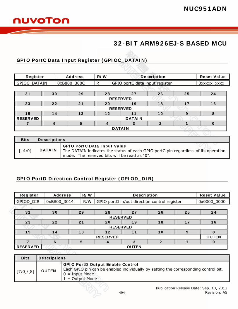
NUC951ADN
32-BIT ARM926EJ-S BASED MCU
Publication Release Date: Sep. 10, 2012 Revision: A5
494
GPIO PortC Data Input Register (GPIOC_DATAIN)
Register Address R/W Description Reset Value
GPIOC_DATAIN 0xB800_300C R GPIO portC data input register 0xxxxx_xxxx
31 30 29 28 27 26 25 24 RESERVED
23 22 21 20 19 18 17 16 RESERVED
15 14 13 12 11 10 9 8 RESERVED DATAIN
7 6 5 4 3 2 1 0 DATAIN
Bits Descriptions
[14:0] DATAIN GPIO PortC Data Input Value The DATAIN indicates the status of each GPIO portC pin regardless of its operation mode. The reserved bits will be read as “0”.
GPIO PortD Direction Control Register (GPIOD_DIR)
Register Address R/W Description Reset Value
GPIOD_DIR 0xB800_3014 R/W GPIO portD in/out direction control register 0x0000_0000
31 30 29 28 27 26 25 24 RESERVED
23 22 21 20 19 18 17 16 RESERVED
15 14 13 12 11 10 9 8 RESERVED OUTEN
7 6 5 4 3 2 1 0 RESERVED OUTEN
Bits Descriptions
[7:0]/[8] OUTEN GPIO PortD Output Enable Control Each GPIO pin can be enabled individually by setting the corresponding control bit. 0 = Input Mode 1 = Output Mode
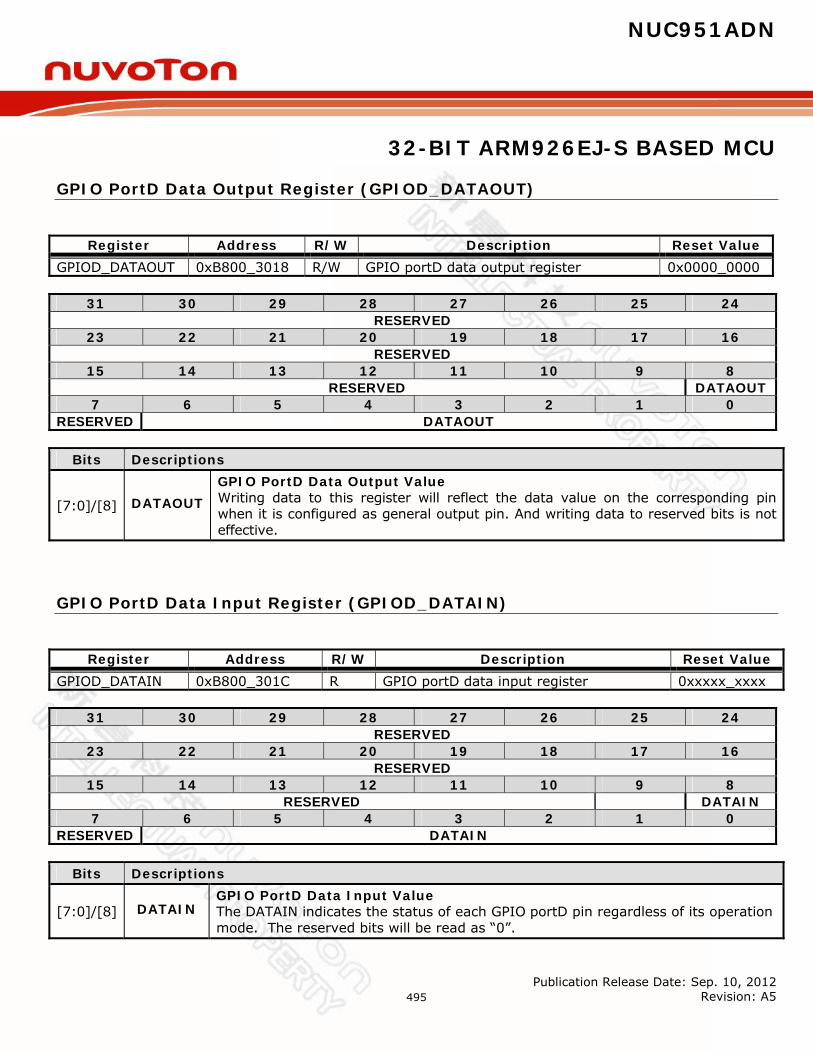
NUC951ADN
32-BIT ARM926EJ-S BASED MCU
Publication Release Date: Sep. 10, 2012 Revision: A5
495
GPIO PortD Data Output Register (GPIOD_DATAOUT)
Register Address R/W Description Reset Value
GPIOD_DATAOUT 0xB800_3018 R/W GPIO portD data output register 0x0000_0000
31 30 29 28 27 26 25 24 RESERVED
23 22 21 20 19 18 17 16 RESERVED
15 14 13 12 11 10 9 8 RESERVED DATAOUT
7 6 5 4 3 2 1 0 RESERVED DATAOUT
Bits Descriptions
[7:0]/[8] DATAOUT GPIO PortD Data Output Value Writing data to this register will reflect the data value on the corresponding pin when it is configured as general output pin. And writing data to reserved bits is not effective.
GPIO PortD Data Input Register (GPIOD_DATAIN)
Register Address R/W Description Reset Value
GPIOD_DATAIN 0xB800_301C R GPIO portD data input register 0xxxxx_xxxx
31 30 29 28 27 26 25 24 RESERVED
23 22 21 20 19 18 17 16 RESERVED
15 14 13 12 11 10 9 8 RESERVED DATAIN
7 6 5 4 3 2 1 0 RESERVED DATAIN
Bits Descriptions
[7:0]/[8] DATAIN GPIO PortD Data Input Value The DATAIN indicates the status of each GPIO portD pin regardless of its operation mode. The reserved bits will be read as “0”.

NUC951ADN
32-BIT ARM926EJ-S BASED MCU
Publication Release Date: Sep. 10, 2012 Revision: A5
496
GPIO PortE Direction Control Register (GPIOE_DIR)
Register Address R/W Description Reset Value
GPIOE_DIR 0xB800_3024 R/W GPIO portE in/out direction control register 0x0000_0000
31 30 29 28 27 26 25 24 RESERVED
23 22 21 20 19 18 17 16 RESERVED
15 14 13 12 11 10 9 8 RESERVED OUTEN RESERVED
7 6 5 4 3 2 1 0 OUTEN RESERVED OUTEN
Bits Descriptions
[3:0]/[7:6] /[13]
OUTEN GPIO PortE Output Enable Control Each GPIO pin can be enabled individually by setting the corresponding control bit. 0 = Input Mode 1 = Output Mode
GPIO PortE Data Output Register (GPIOE_DATAOUT)
Register Address R/W Description Reset Value
GPIOE_DATAOUT 0xB800_3028 R/W GPIO portE data output register 0x0000_0000
31 30 29 28 27 26 25 24 RESERVED
23 22 21 20 19 18 17 16 RESERVED
15 14 13 12 11 10 9 8 RESERVED DATAOUT RESERVED
7 6 5 4 3 2 1 0 DATAOUT RESERVED DATAOUT
Bits Descriptions
[3:0]/[7:6] /[13]
DATAOUT GPIO PortE Data Output Value Writing data to this register will reflect the data value on the corresponding pin when it is configured as general output pin. And writing data to reserved bits is not effective.
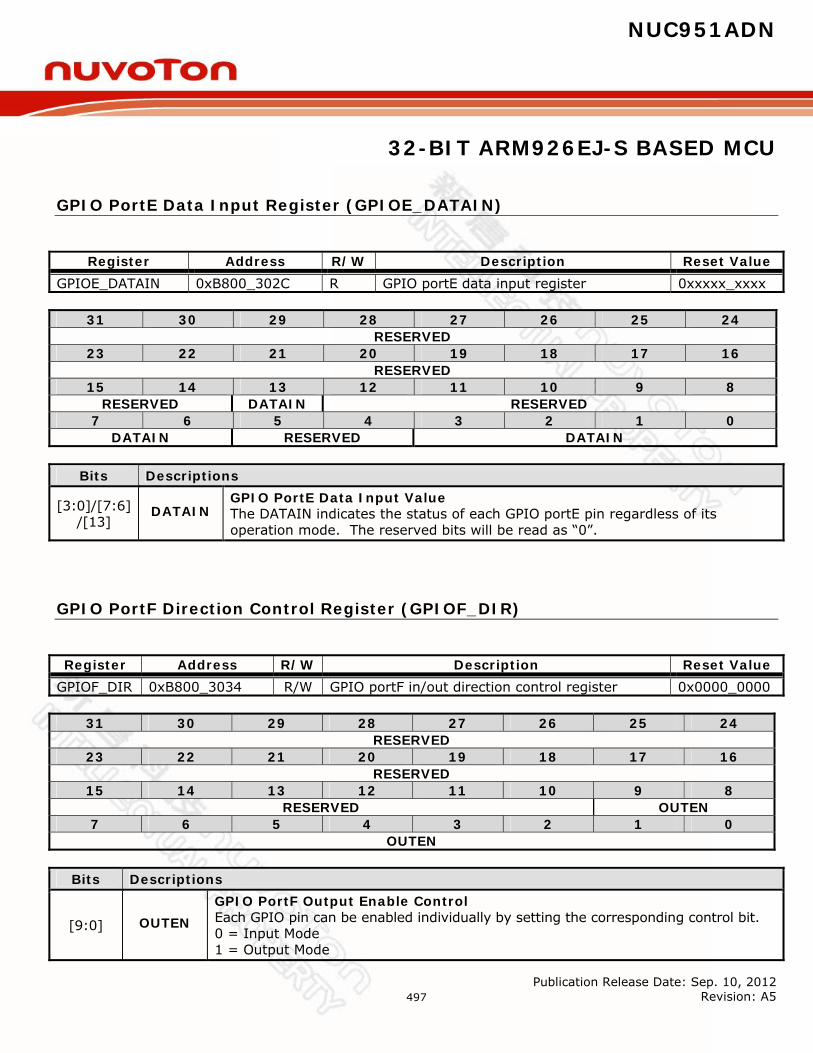
NUC951ADN
32-BIT ARM926EJ-S BASED MCU
Publication Release Date: Sep. 10, 2012 Revision: A5
497
GPIO PortE Data Input Register (GPIOE_DATAIN)
Register Address R/W Description Reset Value
GPIOE_DATAIN 0xB800_302C R GPIO portE data input register 0xxxxx_xxxx
31 30 29 28 27 26 25 24 RESERVED
23 22 21 20 19 18 17 16 RESERVED
15 14 13 12 11 10 9 8 RESERVED DATAIN RESERVED
7 6 5 4 3 2 1 0 DATAIN RESERVED DATAIN
Bits Descriptions
[3:0]/[7:6] /[13]
DATAIN GPIO PortE Data Input Value The DATAIN indicates the status of each GPIO portE pin regardless of its operation mode. The reserved bits will be read as “0”.
GPIO PortF Direction Control Register (GPIOF_DIR)
Register Address R/W Description Reset Value
GPIOF_DIR 0xB800_3034 R/W GPIO portF in/out direction control register 0x0000_0000
31 30 29 28 27 26 25 24 RESERVED
23 22 21 20 19 18 17 16 RESERVED
15 14 13 12 11 10 9 8 RESERVED OUTEN
7 6 5 4 3 2 1 0 OUTEN
Bits Descriptions
[9:0] OUTEN GPIO PortF Output Enable Control Each GPIO pin can be enabled individually by setting the corresponding control bit. 0 = Input Mode 1 = Output Mode
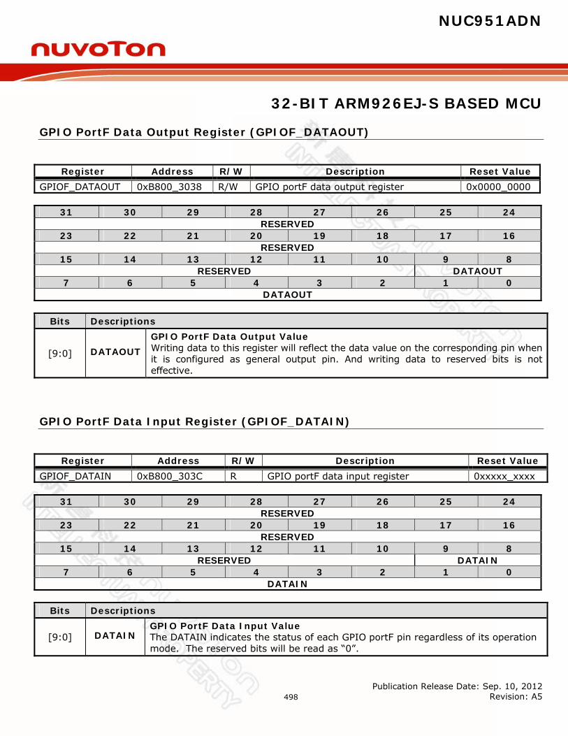
NUC951ADN
32-BIT ARM926EJ-S BASED MCU
Publication Release Date: Sep. 10, 2012 Revision: A5
498
GPIO PortF Data Output Register (GPIOF_DATAOUT)
Register Address R/W Description Reset Value
GPIOF_DATAOUT 0xB800_3038 R/W GPIO portF data output register 0x0000_0000
31 30 29 28 27 26 25 24 RESERVED
23 22 21 20 19 18 17 16 RESERVED
15 14 13 12 11 10 9 8 RESERVED DATAOUT
7 6 5 4 3 2 1 0 DATAOUT
Bits Descriptions
[9:0] DATAOUT GPIO PortF Data Output Value Writing data to this register will reflect the data value on the corresponding pin when it is configured as general output pin. And writing data to reserved bits is not effective.
GPIO PortF Data Input Register (GPIOF_DATAIN)
Register Address R/W Description Reset Value
GPIOF_DATAIN 0xB800_303C R GPIO portF data input register 0xxxxx_xxxx
31 30 29 28 27 26 25 24 RESERVED
23 22 21 20 19 18 17 16 RESERVED
15 14 13 12 11 10 9 8 RESERVED DATAIN
7 6 5 4 3 2 1 0 DATAIN
Bits Descriptions
[9:0] DATAIN GPIO PortF Data Input Value The DATAIN indicates the status of each GPIO portF pin regardless of its operation mode. The reserved bits will be read as “0”.
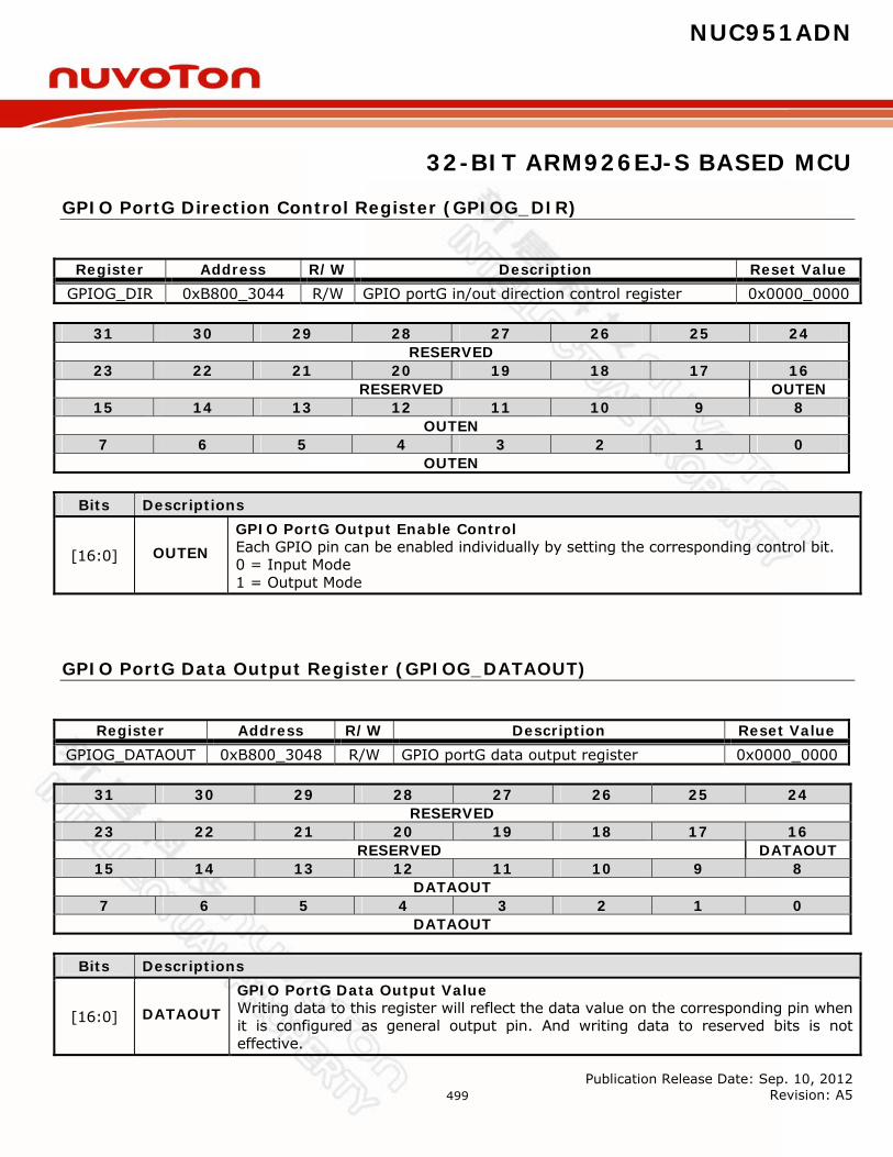
NUC951ADN
32-BIT ARM926EJ-S BASED MCU
Publication Release Date: Sep. 10, 2012 Revision: A5
499
GPIO PortG Direction Control Register (GPIOG_DIR)
Register Address R/W Description Reset Value
GPIOG_DIR 0xB800_3044 R/W GPIO portG in/out direction control register 0x0000_0000
31 30 29 28 27 26 25 24 RESERVED
23 22 21 20 19 18 17 16 RESERVED OUTEN
15 14 13 12 11 10 9 8 OUTEN
7 6 5 4 3 2 1 0 OUTEN
Bits Descriptions
[16:0] OUTEN GPIO PortG Output Enable Control Each GPIO pin can be enabled individually by setting the corresponding control bit. 0 = Input Mode 1 = Output Mode
GPIO PortG Data Output Register (GPIOG_DATAOUT)
Register Address R/W Description Reset Value
GPIOG_DATAOUT 0xB800_3048 R/W GPIO portG data output register 0x0000_0000
31 30 29 28 27 26 25 24 RESERVED
23 22 21 20 19 18 17 16 RESERVED DATAOUT
15 14 13 12 11 10 9 8 DATAOUT
7 6 5 4 3 2 1 0 DATAOUT
Bits Descriptions
[16:0] DATAOUT GPIO PortG Data Output Value Writing data to this register will reflect the data value on the corresponding pin when it is configured as general output pin. And writing data to reserved bits is not effective.

NUC951ADN
32-BIT ARM926EJ-S BASED MCU
Publication Release Date: Sep. 10, 2012 Revision: A5
500
GPIO PortG Data Input Register (GPIOG_DATAIN)
Register Address R/W Description Reset Value
GPIOG_DATAIN 0xB800_304C R GPIO portG data input register 0xxxxx_xxxx
31 30 29 28 27 26 25 24 RESERVED
23 22 21 20 19 18 17 16 RESERVED DATAIN
15 14 13 12 11 10 9 8 DATAIN
7 6 5 4 3 2 1 0 DATAIN
Bits Descriptions
[16:0] DATAIN GPIO PortG Data Input Value The DATAIN indicates the status of each GPIO portG pin regardless of its operation mode. The reserved bits will be read as “0”.
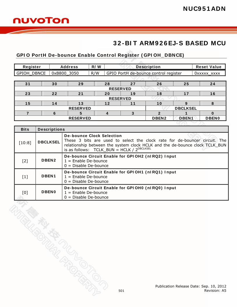
NUC951ADN
32-BIT ARM926EJ-S BASED MCU
Publication Release Date: Sep. 10, 2012 Revision: A5
501
GPIO PortH De-bounce Enable Control Register (GPIOH_DBNCE)
Register Address R/W Description Reset Value GPIOH_DBNCE 0xB800_3050 R/W GPIO PortH de-bounce control register 0xxxxx_xxxx
31 30 29 28 27 26 25 24 RESERVED
23 22 21 20 19 18 17 16 RESERVED
15 14 13 12 11 10 9 8 RESERVED DBCLKSEL
7 6 5 4 3 2 1 0 RESERVED DBEN2 DBEN1 DBEN0
Bits Descriptions
[10:8] DBCLKSEL De-bounce Clock Selection These 3 bits are used to select the clock rate for de-bouncer circuit. The relationship between the system clock HCLK and the de-bounce clock TCLK_BUN is as follows: TCLK_BUN = HCLK / 2DBCLKSEL
[2] DBEN2 De-bounce Circuit Enable for GPIOH2 (nIRQ2) Input 1 = Enable De-bounce 0 = Disable De-bounce
[1] DBEN1 De-bounce Circuit Enable for GPIOH1 (nIRQ1) Input 1 = Enable De-bounce 0 = Disable De-bounce
[0] DBEN0 De-bounce Circuit Enable for GPIOH0 (nIRQ0) Input 1 = Enable De-bounce 0 = Disable De-bounce

NUC951ADN
32-BIT ARM926EJ-S BASED MCU
Publication Release Date: Sep. 10, 2012 Revision: A5
502
GPIO PortH Direction Control Register (GPIOH_DIR)
Register Address R/W Description Reset Value
GPIOH_DIR 0xB800_3054 R/W GPIO portH in/out direction control register 0x0000_0000
31 30 29 28 27 26 25 24 RESERVED
23 22 21 20 19 18 17 16 RESERVED
15 14 13 12 11 10 9 8 RESERVED
7 6 5 4 3 2 1 0 RESERVED OUTEN
Bits Descriptions
[2:0] OUTEN GPIO PortH Output Enable Control Each GPIO pin can be enabled individually by setting the corresponding control bit. 0 = Input Mode 1 = Output Mode
GPIO PortH Data Output Register (GPIOH_DATAOUT)
Register Address R/W Description Reset Value GPIOH_DATAOUT 0xB800_3058 R/W GPIO portH data output register 0x0000_0000
31 30 29 28 27 26 25 24 RESERVED
23 22 21 20 19 18 17 16 RESERVED
15 14 13 12 11 10 9 8 RESERVED
7 6 5 4 3 2 1 0 RESERVED DATAOUT
Bits Descriptions
[2:0] DATAOUT GPIO PortH Data Output Value Writing data to this register will reflect the data value on the corresponding pin when it is configured as general output pin. And writing data to reserved bits is not effective.
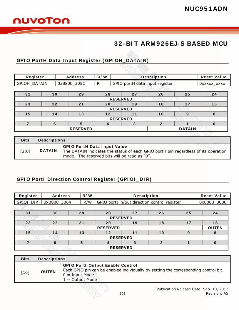
NUC951ADN
32-BIT ARM926EJ-S BASED MCU
Publication Release Date: Sep. 10, 2012 Revision: A5
503
GPIO PortH Data Input Register (GPIOH_DATAIN)
Register Address R/W Description Reset Value
GPIOH_DATAIN 0xB800_305C R GPIO portH data input register 0xxxxx_xxxx
31 30 29 28 27 26 25 24 RESERVED
23 22 21 20 19 18 17 16 RESERVED
15 14 13 12 11 10 9 8 RESERVED
7 6 5 4 3 2 1 0 RESERVED DATAIN
Bits Descriptions
[2:0] DATAIN GPIO PortH Data Input Value The DATAIN indicates the status of each GPIO portH pin regardless of its operation mode. The reserved bits will be read as “0”.
GPIO PortI Direction Control Register (GPIOI_DIR)
Register Address R/W Description Reset Value
GPIOI_DIR 0xB800_3064 R/W GPIO portI in/out direction control register 0x0000_0000
31 30 29 28 27 26 25 24 RESERVED
23 22 21 20 19 18 17 16 RESERVED OUTEN
15 14 13 12 11 10 9 8 RESERVED
7 6 5 4 3 2 1 0 RESERVED
Bits Descriptions
[16] OUTEN GPIO PortI Output Enable Control Each GPIO pin can be enabled individually by setting the corresponding control bit. 0 = Input Mode 1 = Output Mode
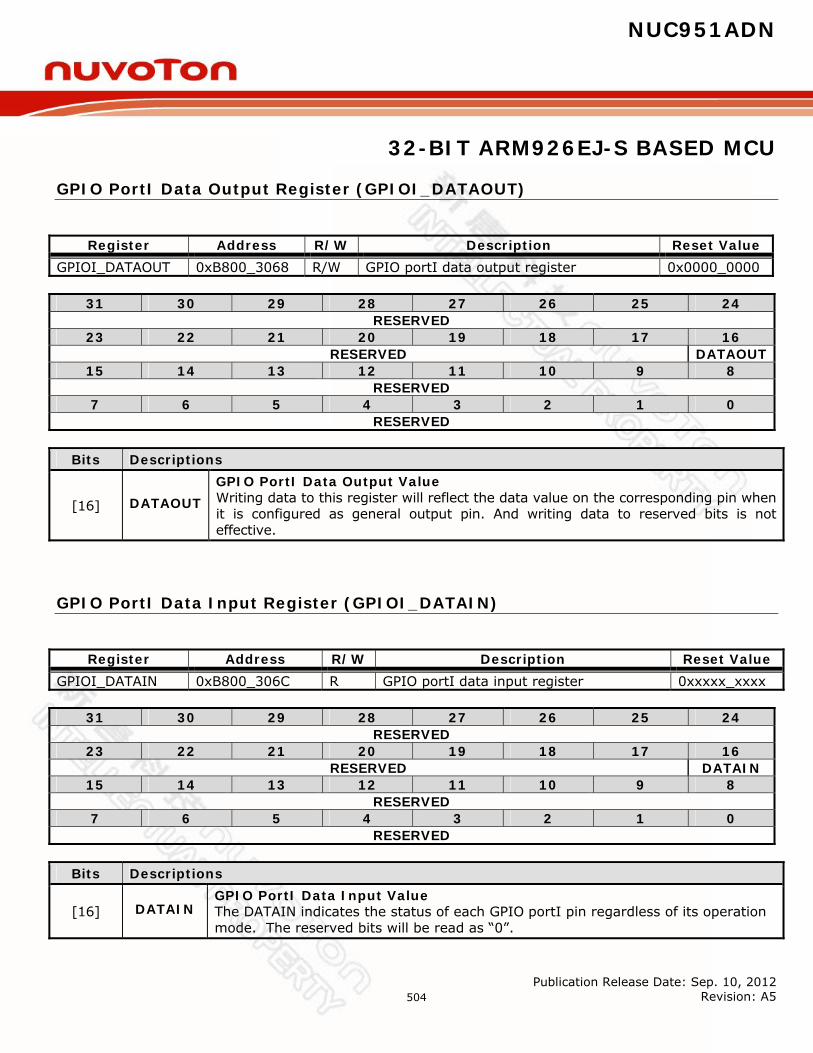
NUC951ADN
32-BIT ARM926EJ-S BASED MCU
Publication Release Date: Sep. 10, 2012 Revision: A5
504
GPIO PortI Data Output Register (GPIOI_DATAOUT)
Register Address R/W Description Reset Value
GPIOI_DATAOUT 0xB800_3068 R/W GPIO portI data output register 0x0000_0000
31 30 29 28 27 26 25 24 RESERVED
23 22 21 20 19 18 17 16 RESERVED DATAOUT
15 14 13 12 11 10 9 8 RESERVED
7 6 5 4 3 2 1 0 RESERVED
Bits Descriptions
[16] DATAOUT GPIO PortI Data Output Value Writing data to this register will reflect the data value on the corresponding pin when it is configured as general output pin. And writing data to reserved bits is not effective.
GPIO PortI Data Input Register (GPIOI_DATAIN)
Register Address R/W Description Reset Value
GPIOI_DATAIN 0xB800_306C R GPIO portI data input register 0xxxxx_xxxx
31 30 29 28 27 26 25 24 RESERVED
23 22 21 20 19 18 17 16 RESERVED DATAIN
15 14 13 12 11 10 9 8 RESERVED
7 6 5 4 3 2 1 0 RESERVED
Bits Descriptions
[16] DATAIN GPIO PortI Data Input Value The DATAIN indicates the status of each GPIO portI pin regardless of its operation mode. The reserved bits will be read as “0”.
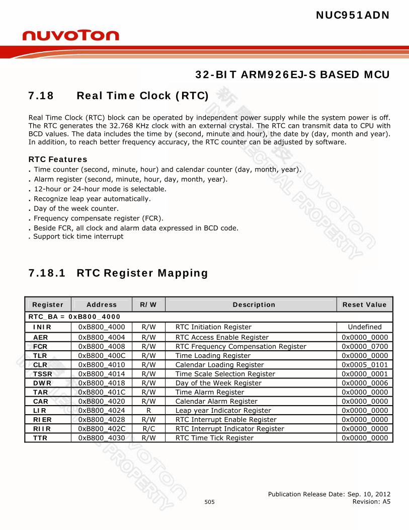
NUC951ADN
32-BIT ARM926EJ-S BASED MCU
Publication Release Date: Sep. 10, 2012 Revision: A5
505
7.18 Real Time Clock (RTC) Real Time Clock (RTC) block can be operated by independent power supply while the system power is off. The RTC generates the 32.768 KHz clock with an external crystal. The RTC can transmit data to CPU with BCD values. The data includes the time by (second, minute and hour), the date by (day, month and year). In addition, to reach better frequency accuracy, the RTC counter can be adjusted by software. RTC Features . Time counter (second, minute, hour) and calendar counter (day, month, year). . Alarm register (second, minute, hour, day, month, year). . 12-hour or 24-hour mode is selectable. . Recognize leap year automatically. . Day of the week counter. . Frequency compensate register (FCR). . Beside FCR, all clock and alarm data expressed in BCD code. . Support tick time interrupt
7.18.1 RTC Register Mapping
Register Address R/W Description Reset Value
RTC_BA = 0xB800_4000 INIR 0xB800_4000 R/W RTC Initiation Register Undefined AER 0xB800_4004 R/W RTC Access Enable Register 0x0000_0000 FCR 0xB800_4008 R/W RTC Frequency Compensation Register 0x0000_0700 TLR 0xB800_400C R/W Time Loading Register 0x0000_0000 CLR 0xB800_4010 R/W Calendar Loading Register 0x0005_0101 TSSR 0xB800_4014 R/W Time Scale Selection Register 0x0000_0001 DWR 0xB800_4018 R/W Day of the Week Register 0x0000_0006 TAR 0xB800_401C R/W Time Alarm Register 0x0000_0000 CAR 0xB800_4020 R/W Calendar Alarm Register 0x0000_0000 LIR 0xB800_4024 R Leap year Indicator Register 0x0000_0000 RIER 0xB800_4028 R/W RTC Interrupt Enable Register 0x0000_0000 RIIR 0xB800_402C R/C RTC Interrupt Indicator Register 0x0000_0000 TTR 0xB800_4030 R/W RTC Time Tick Register 0x0000_0000

NUC951ADN
32-BIT ARM926EJ-S BASED MCU
Publication Release Date: Sep. 10, 2012 Revision: A5
506
RTC Initiation Register (INIR)
Register Address R/W Description Reset Value
INIR 0xB800_4000 R/W RTC Initiation Register 0x0000_0000
31 30 29 28 27 26 25 24 INIR
23 22 21 20 19 18 17 16 INIR
15 14 13 12 11 10 9 8 INIR
7 6 5 4 3 2 1 0 INIR
Bits Descriptions
[31:0] INIR
INIR [31:0]: The INIR register is used to replace hardware reset circuit. User must write INIR as “0xa5eb_1357” after RTC is power on. INIR [0]: R/W. Once RTC INIR has been written, user can access this bit to find out whether RTC reset signal is pulled high.

NUC951ADN
32-BIT ARM926EJ-S BASED MCU
Publication Release Date: Sep. 10, 2012 Revision: A5
507
RTC Access Enable Register (AER)
Register Address R/W Description Reset Value
AER 0xB800_4004 R/W RTC Access Enable Register 0x0000_0000
31 30 29 28 27 26 25 24 RESERVED
23 22 21 20 19 18 17 16 RESERVED AER
15 14 13 12 11 10 9 8 AER
7 6 5 4 3 2 1 0 AER
Bits Descriptions
[16:0] AER
AER [16]: Read only 1 = RTC register write enable 0 = RTC register write disable AER[15:0]: Write only RTC register write enable/disable password 0xa965 = write enable 0x0000 = write disable
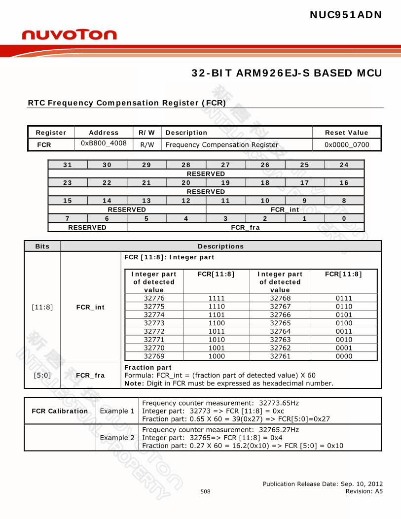
NUC951ADN
32-BIT ARM926EJ-S BASED MCU
Publication Release Date: Sep. 10, 2012 Revision: A5
508
RTC Frequency Compensation Register (FCR)
Register Address R/W Description Reset Value
FCR 0xB800_4008 R/W Frequency Compensation Register 0x0000_0700
31 30 29 28 27 26 25 24 RESERVED
23 22 21 20 19 18 17 16 RESERVED
15 14 13 12 11 10 9 8 RESERVED FCR_int
7 6 5 4 3 2 1 0 RESERVED FCR_fra
Bits Descriptions
[11:8] FCR_int
FCR [11:8]: Integer part
Integer part of detected
value
FCR[11:8] Integer part of detected
value
FCR[11:8]
32776 1111 32768 0111 32775 1110 32767 0110 32774 1101 32766 0101 32773 1100 32765 0100 32772 1011 32764 0011 32771 1010 32763 0010 32770 1001 32762 0001 32769 1000 32761 0000
[5:0] FCR_fra Fraction part Formula: FCR_int = (fraction part of detected value) X 60 Note: Digit in FCR must be expressed as hexadecimal number.
FCR Calibration Example 1 Frequency counter measurement: 32773.65Hz Integer part: 32773 => FCR [11:8] = 0xc Fraction part: 0.65 X 60 = 39(0x27) => FCR[5:0]=0x27
Example 2 Frequency counter measurement: 32765.27Hz Integer part: 32765=> FCR [11:8] = 0x4 Fraction part: 0.27 X 60 = 16.2(0x10) => FCR [5:0] = 0x10
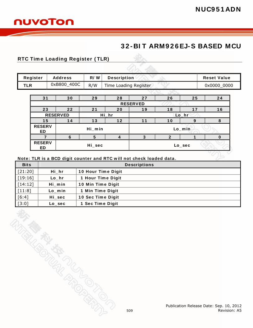
NUC951ADN
32-BIT ARM926EJ-S BASED MCU
Publication Release Date: Sep. 10, 2012 Revision: A5
509
RTC Time Loading Register (TLR)
Register Address R/W Description Reset Value
TLR 0xB800_400C R/W Time Loading Register 0x0000_0000
31 30 29 28 27 26 25 24 RESERVED
23 22 21 20 19 18 17 16 RESERVED Hi_hr Lo_hr
15 14 13 12 11 10 9 8 RESERV
ED Hi_min Lo_min
7 6 5 4 3 2 1 0 RESERV
ED Hi_sec Lo_sec
Note: TLR is a BCD digit counter and RTC will not check loaded data.
Bits Descriptions [21:20] Hi_hr 10 Hour Time Digit [19:16] Lo_hr 1 Hour Time Digit [14:12] Hi_min 10 Min Time Digit [11:8] Lo_min 1 Min Time Digit [6:4] Hi_sec 10 Sec Time Digit [3:0] Lo_sec 1 Sec Time Digit
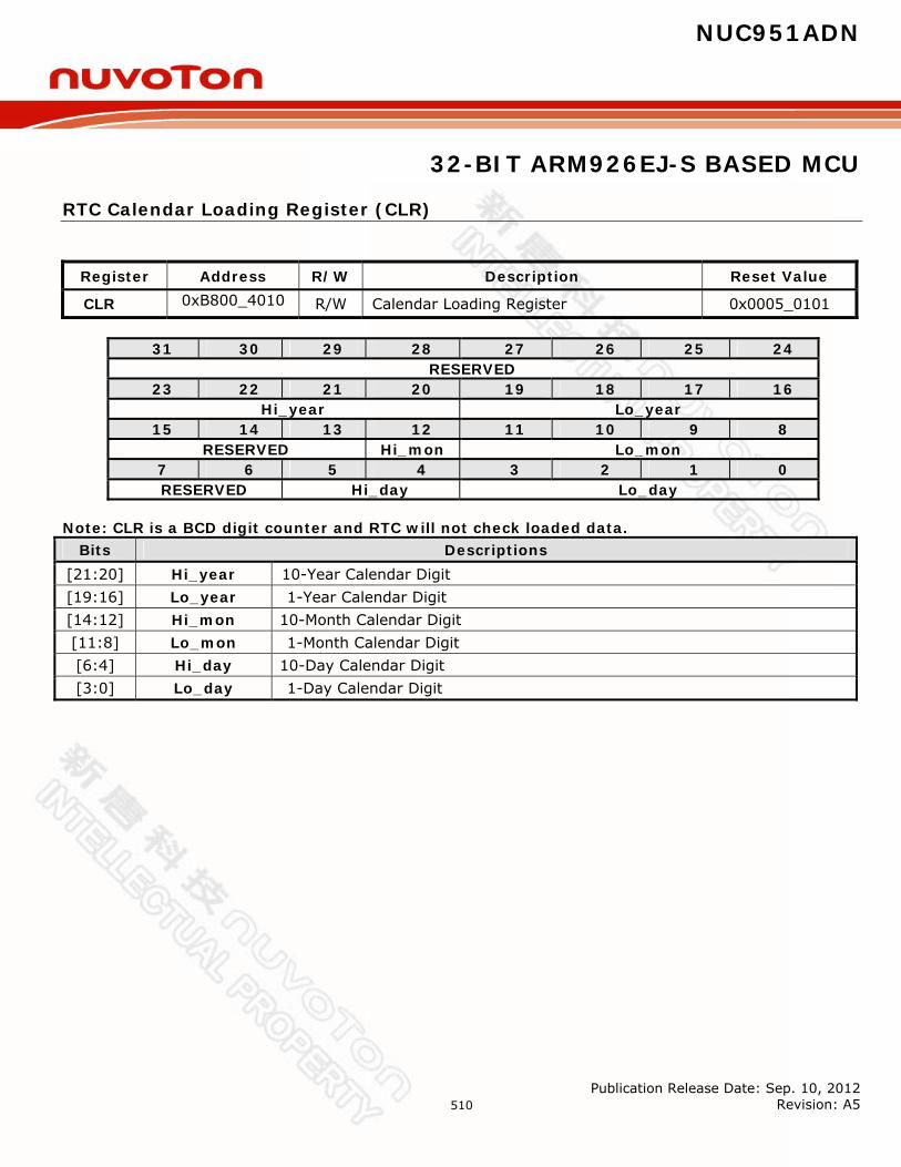
NUC951ADN
32-BIT ARM926EJ-S BASED MCU
Publication Release Date: Sep. 10, 2012 Revision: A5
510
RTC Calendar Loading Register (CLR)
Register Address R/W Description Reset Value
CLR 0xB800_4010 R/W Calendar Loading Register 0x0005_0101
31 30 29 28 27 26 25 24 RESERVED
23 22 21 20 19 18 17 16 Hi_year Lo_year
15 14 13 12 11 10 9 8 RESERVED Hi_mon Lo_mon
7 6 5 4 3 2 1 0 RESERVED Hi_day Lo_day
Note: CLR is a BCD digit counter and RTC will not check loaded data.
Bits Descriptions [21:20] Hi_year 10-Year Calendar Digit [19:16] Lo_year 1-Year Calendar Digit [14:12] Hi_mon 10-Month Calendar Digit [11:8] Lo_mon 1-Month Calendar Digit [6:4] Hi_day 10-Day Calendar Digit [3:0] Lo_day 1-Day Calendar Digit
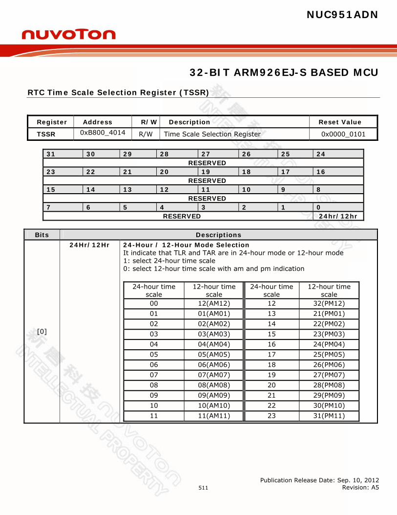
NUC951ADN
32-BIT ARM926EJ-S BASED MCU
Publication Release Date: Sep. 10, 2012 Revision: A5
511
RTC Time Scale Selection Register (TSSR)
Register Address R/W Description Reset Value
TSSR 0xB800_4014 R/W Time Scale Selection Register 0x0000_0101
31 30 29 28 27 26 25 24 RESERVED
23 22 21 20 19 18 17 16 RESERVED
15 14 13 12 11 10 9 8 RESERVED
7 6 5 4 3 2 1 0 RESERVED 24hr/12hr
Bits Descriptions
[0]
24Hr/12Hr 24-Hour / 12-Hour Mode Selection It indicate that TLR and TAR are in 24-hour mode or 12-hour mode 1: select 24-hour time scale 0: select 12-hour time scale with am and pm indication
24-hour time scale
12-hour time scale
24-hour time scale
12-hour time scale
00 12(AM12) 12 32(PM12) 01 01(AM01) 13 21(PM01) 02 02(AM02) 14 22(PM02) 03 03(AM03) 15 23(PM03) 04 04(AM04) 16 24(PM04) 05 05(AM05) 17 25(PM05) 06 06(AM06) 18 26(PM06) 07 07(AM07) 19 27(PM07) 08 08(AM08) 20 28(PM08) 09 09(AM09) 21 29(PM09) 10 10(AM10) 22 30(PM10) 11 11(AM11) 23 31(PM11)
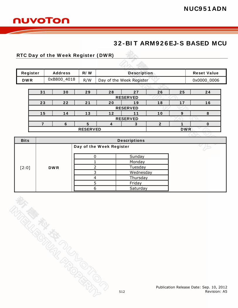
NUC951ADN
32-BIT ARM926EJ-S BASED MCU
Publication Release Date: Sep. 10, 2012 Revision: A5
512
RTC Day of the Week Register (DWR)
Register Address R/W Description Reset Value
DWR 0xB800_4018 R/W Day of the Week Register 0x0000_0006
31 30 29 28 27 26 25 24 RESERVED
23 22 21 20 19 18 17 16 RESERVED
15 14 13 12 11 10 9 8 RESERVED
7 6 5 4 3 2 1 0 RESERVED DWR
Bits Descriptions
[2:0] DWR
Day of the Week Register
0 Sunday 1 Monday 2 Tuesday 3 Wednesday 4 Thursday 5 Friday 6 Saturday
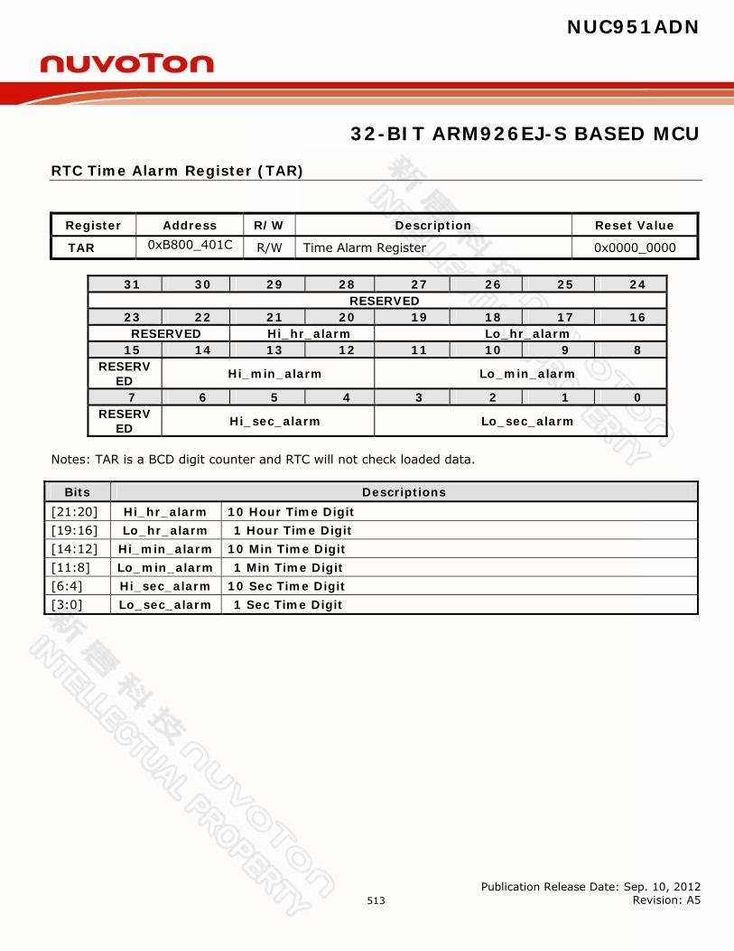
NUC951ADN
32-BIT ARM926EJ-S BASED MCU
Publication Release Date: Sep. 10, 2012 Revision: A5
513
RTC Time Alarm Register (TAR)
Register Address R/W Description Reset Value
TAR 0xB800_401C R/W Time Alarm Register 0x0000_0000
31 30 29 28 27 26 25 24 RESERVED
23 22 21 20 19 18 17 16 RESERVED Hi_hr_alarm Lo_hr_alarm
15 14 13 12 11 10 9 8 RESERV
ED Hi_min_alarm Lo_min_alarm
7 6 5 4 3 2 1 0 RESERV
ED Hi_sec_alarm Lo_sec_alarm
Notes: TAR is a BCD digit counter and RTC will not check loaded data.
Bits Descriptions [21:20] Hi_hr_alarm 10 Hour Time Digit [19:16] Lo_hr_alarm 1 Hour Time Digit [14:12] Hi_min_alarm 10 Min Time Digit [11:8] Lo_min_alarm 1 Min Time Digit [6:4] Hi_sec_alarm 10 Sec Time Digit [3:0] Lo_sec_alarm 1 Sec Time Digit

NUC951ADN
32-BIT ARM926EJ-S BASED MCU
Publication Release Date: Sep. 10, 2012 Revision: A5
514
RTC Calendar Alarm Register (CAR)
Register Address R/W Description Reset Value
CAR 0xB800_4020 R/W Calendar Alarm Register 0x0005_0101
31 30 29 28 27 26 25 24 RESERVED
23 22 21 20 19 18 17 16 Hi_year_alarm Lo_year_alarm
15 14 13 12 11 10 9 8
RESERVED Hi_mon_ alarm Lo_mon_alarm
7 6 5 4 3 2 1 0 RESERVED Hi_day_alarm Lo_day_alarm
Bits Descriptions
[21:20] Hi_year 10-Year Calendar Digit [19:16] Lo_year 1-Year Calendar Digit [14:12] Hi_mon 10-Month Calendar Digit [11:8] Lo_mon 1-Month Calendar Digit [6:4] Hi_day 10-Day Calendar Digit [3:0] Lo_day 1-Day Calendar Digit
Notes: CAR is a BCD digit counter and RTC will not check loaded data.

NUC951ADN
32-BIT ARM926EJ-S BASED MCU
Publication Release Date: Sep. 10, 2012 Revision: A5
515
RTC Leap year Indication Register (LIR)
Register Address R/W Description Reset Value
LIR 0xB800_4024 R RTC Leap year Indication Register 0x0000_0000
31 30 29 28 27 26 25 24 RESERVED
23 22 21 20 19 18 17 16 RESERVED
15 14 13 12 11 10 9 8 RESERVED
7 6 5 4 3 2 1 0 RESERVED LIR
Bits Descriptions
[0] LIR
LIR [0]: Real only. Leap year Indication REGISTER 1 : It indicate that this year is leap year 0 : It indicate that this year is not a leap year
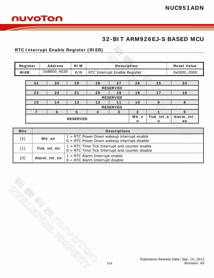
NUC951ADN
32-BIT ARM926EJ-S BASED MCU
Publication Release Date: Sep. 10, 2012 Revision: A5
516
RTC Interrupt Enable Register (RIER)
Register Address R/W Description Reset Value
RIER 0xB800_4028 R/W RTC Interrupt Enable Register 0x0000_0000
31 30 29 28 27 26 25 24 RESERVED
23 22 21 20 19 18 17 16 RESERVED
15 14 13 12 11 10 9 8 RESERVED
7 6 5 4 3 2 1 0
RESERVED Wk_en
Tick_int_en
Alarm_int_en
Bits Descriptions
[2] Wk_en 1 = RTC Power Down wakeup interrupt enable 0 = RTC Power Down wakeup interrupt disable
[1] Tick_int_en 1 = RTC Time Tick Interrupt and counter enable 0 = RTC Time Tick Interrupt and counter disable
[0] Alarm_int_en 1 = RTC Alarm Interrupt enable 0 = RTC Alarm Interrupt disable

NUC951ADN
32-BIT ARM926EJ-S BASED MCU
Publication Release Date: Sep. 10, 2012 Revision: A5
517
RTC Interrupt Indication Register (RIIR)
Register Address R/W Description Reset Value
RIER 0xB800_4028 R/C RTC Interrupt Indication Register 0x0000_0000
31 30 29 28 27 26 25 24 RESERVED
23 22 21 20 19 18 17 16 RESERVED
15 14 13 12 11 10 9 8 RESERVED
7 6 5 4 3 2 1 0
RESERVED Wk_st Tick_int_st
Alarm_int_st
Bits Descriptions
[2] Wk_st
1 = It indicates that RTC time alarm and calendar alarm has been activated. System clock is wakeup from power down mode.
0 = It indicates that system clock has been wakeup from power down mode. Software can clear this bit by writing “1” after RTC wakeup interrupt has occurred.
[1] Tick_int_st
RTC Time Tick Interrupt Indication REGISTER 1 = It indicates that time tick interrupt has been activated. 0 = It indicates that time tick interrupt has never occurred. Software can also clear this bit after RTC interrupt has occur.
[0] Alarm_int_st
RTC Alarm Interrupt Indication REGISTER 1 = It indicates that time counter and calendar counter have counted to a
specified time recorded in TAR and CAR. RTC alarm interrupt has been activated.
0 = It indicates that alarm interrupt has never occurred. Software can also clear this bit after RTC interrupt has occurred.
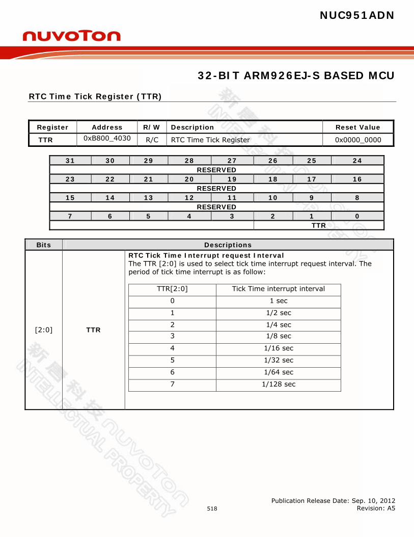
NUC951ADN
32-BIT ARM926EJ-S BASED MCU
Publication Release Date: Sep. 10, 2012 Revision: A5
518
RTC Time Tick Register (TTR)
Register Address R/W Description Reset Value
TTR 0xB800_4030 R/C RTC Time Tick Register 0x0000_0000
31 30 29 28 27 26 25 24 RESERVED
23 22 21 20 19 18 17 16 RESERVED
15 14 13 12 11 10 9 8 RESERVED
7 6 5 4 3 2 1 0 TTR
Bits Descriptions
[2:0] TTR
RTC Tick Time Interrupt request Interval The TTR [2:0] is used to select tick time interrupt request interval. The period of tick time interrupt is as follow:
TTR[2:0] Tick Time interrupt interval
0 1 sec
1 1/2 sec
2 1/4 sec 3 1/8 sec
4 1/16 sec
5 1/32 sec
6 1/64 sec
7 1/128 sec

NUC951ADN
32-BIT ARM926EJ-S BASED MCU
Publication Release Date: Sep. 10, 2012 Revision: A5
519
7.19 I2C Synchronous Serial Interface Controller I2C is a two-wire, bi-directional serial bus that provides a simple and efficient method of data exchange between devices. The I2C standard is a true multi-master bus including collision detection and arbitration that prevents data corruption if two or more masters attempt to control the bus simultaneously. Serial, 8-bit oriented bi-directional data transfers can be up to 100 Kb/s in Standard-mode, 400 Kb/s in the Fast-mode, or 3.4 Mb/s in the High-speed mode. Only 100kbps and 400kbps modes are supported directly in this chip. Data transfer is synchronized to SCL signal between a Master and a Slave with byte-by-byte basis. Each data byte is 8 bits long. There is one SCL clock pulse for each data bit with the MSB being transmitted first. An acknowledge bit follows each transferred byte. Each bit is sampled during the high period of SCL; therefore, the SDA line may be changed only during the low period of SCL and must be held stable during the high period of SCL. A transition on the SDA line while SCL is high is interpreted as a command (START or STOP). The I2C Master Core includes the following features:
Compatible with I2C standard, support master mode
Multi Master Operation.
Clock stretching and wait state generation.
Provide multi-byte transmit operation, up to 4 bytes can be transmitted in a single transfer
Software programmable acknowledge bit.
Arbitration lost interrupt, with automatic transfer cancellation.
Start/Stop/Repeated Start/Acknowledge generation.
Start/Stop/Repeated Start detection.
Bus busy detection.
Supports 7 bit addressing mode.
Fully static synchronous design with one clock domain.
Software mode I2C.
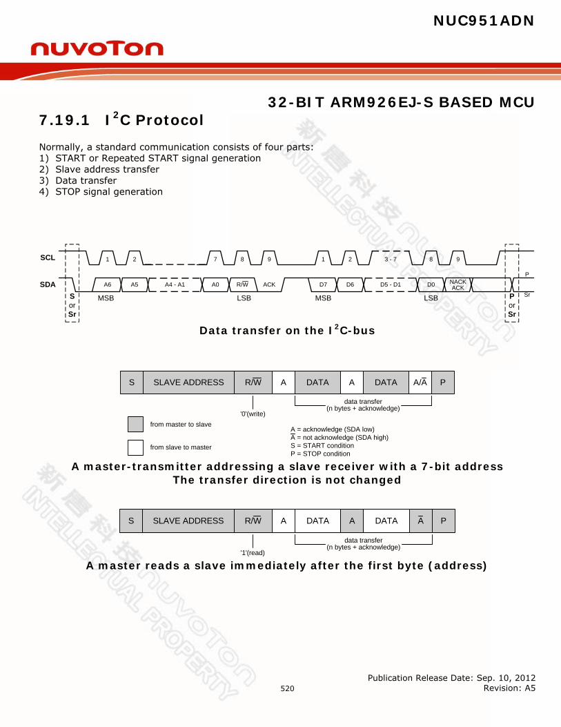
NUC951ADN
32-BIT ARM926EJ-S BASED MCU
Publication Release Date: Sep. 10, 2012 Revision: A5
520
7.19.1 I2C Protocol Normally, a standard communication consists of four parts: 1) START or Repeated START signal generation 2) Slave address transfer 3) Data transfer 4) STOP signal generation
SCL
SDA
SorSr
MSB
ACK
PorSr
P
SrLSB MSB LSB
1 2 7 8 9 1 2 3 - 7 8 9
A6 A5 A4 - A1 A0 R/W D7 D6 D5 - D1 D0 NACKACK
Data transfer on the I2C-bus
S SLAVE ADDRESS R/W A DATA A DATA A/A P
'0'(write)
data transfer(n bytes + acknowledge)
from master to slave
from slave to master
A = acknowledge (SDA low)A = not acknowledge (SDA high)S = START conditionP = STOP condition
A master-transmitter addressing a slave receiver with a 7-bit address The transfer direction is not changed
'1'(read)
data transfer(n bytes + acknowledge)
S SLAVE ADDRESS R/W A DATA A DATA A P
A master reads a slave immediately after the first byte (address)
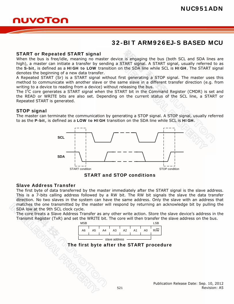
NUC951ADN
32-BIT ARM926EJ-S BASED MCU
Publication Release Date: Sep. 10, 2012 Revision: A5
521
START or Repeated START signal When the bus is free/idle, meaning no master device is engaging the bus (both SCL and SDA lines are high), a master can initiate a transfer by sending a START signal. A START signal, usually referred to as the S-bit, is defined as a HIGH to LOW transition on the SDA line while SCL is HIGH. The START signal denotes the beginning of a new data transfer. A Repeated START (Sr) is a START signal without first generating a STOP signal. The master uses this method to communicate with another slave or the same slave in a different transfer direction (e.g. from writing to a device to reading from a device) without releasing the bus. The I2C core generates a START signal when the START bit in the Command Register (CMDR) is set and the READ or WRITE bits are also set. Depending on the current status of the SCL line, a START or Repeated START is generated. STOP signal The master can terminate the communication by generating a STOP signal. A STOP signal, usually referred to as the P-bit, is defined as a LOW to HIGH transition on the SDA line while SCL is HIGH.
START condition STOP condition
SCL
SDA
START and STOP conditions
Slave Address Transfer The first byte of data transferred by the master immediately after the START signal is the slave address. This is a 7-bits calling address followed by a RW bit. The RW bit signals the slave the data transfer direction. No two slaves in the system can have the same address. Only the slave with an address that matches the one transmitted by the master will respond by returning an acknowledge bit by pulling the SDA low at the 9th SCL clock cycle. The core treats a Slave Address Transfer as any other write action. Store the slave device’s address in the Transmit Register (TxR) and set the WRITE bit. The core will then transfer the slave address on the bus.
MSB LSB
R/WA0A1A2A3A4A5A6
slave address The first byte after the START procedure
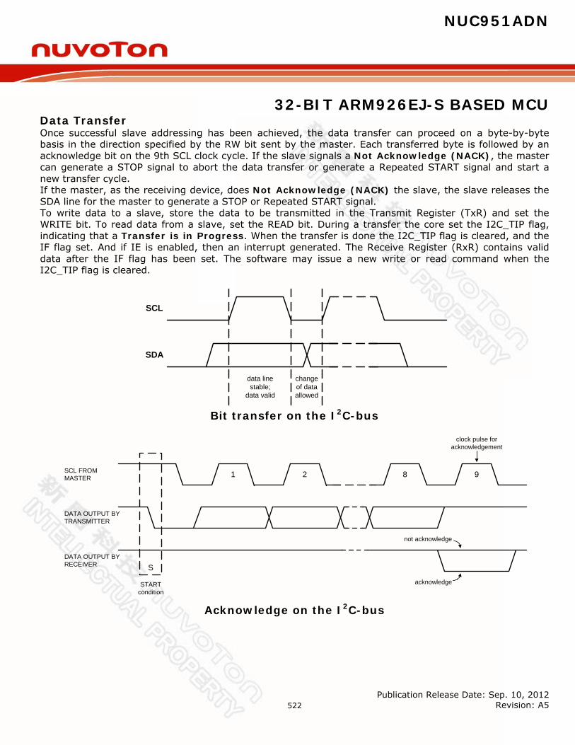
NUC951ADN
32-BIT ARM926EJ-S BASED MCU
Publication Release Date: Sep. 10, 2012 Revision: A5
522
Data Transfer Once successful slave addressing has been achieved, the data transfer can proceed on a byte-by-byte basis in the direction specified by the RW bit sent by the master. Each transferred byte is followed by an acknowledge bit on the 9th SCL clock cycle. If the slave signals a Not Acknowledge (NACK), the master can generate a STOP signal to abort the data transfer or generate a Repeated START signal and start a new transfer cycle. If the master, as the receiving device, does Not Acknowledge (NACK) the slave, the slave releases the SDA line for the master to generate a STOP or Repeated START signal. To write data to a slave, store the data to be transmitted in the Transmit Register (TxR) and set the WRITE bit. To read data from a slave, set the READ bit. During a transfer the core set the I2C_TIP flag, indicating that a Transfer is in Progress. When the transfer is done the I2C_TIP flag is cleared, and the IF flag set. And if IE is enabled, then an interrupt generated. The Receive Register (RxR) contains valid data after the IF flag has been set. The software may issue a new write or read command when the I2C_TIP flag is cleared.
data linestable;
data valid
changeof dataallowed
SCL
SDA
Bit transfer on the I2C-bus
1 2 8 9SCL FROMMASTER
DATA OUTPUT BYTRANSMITTER
DATA OUTPUT BYRECEIVER S
STARTcondition
clock pulse foracknowledgement
not acknowledge
acknowledge
Acknowledge on the I2C-bus
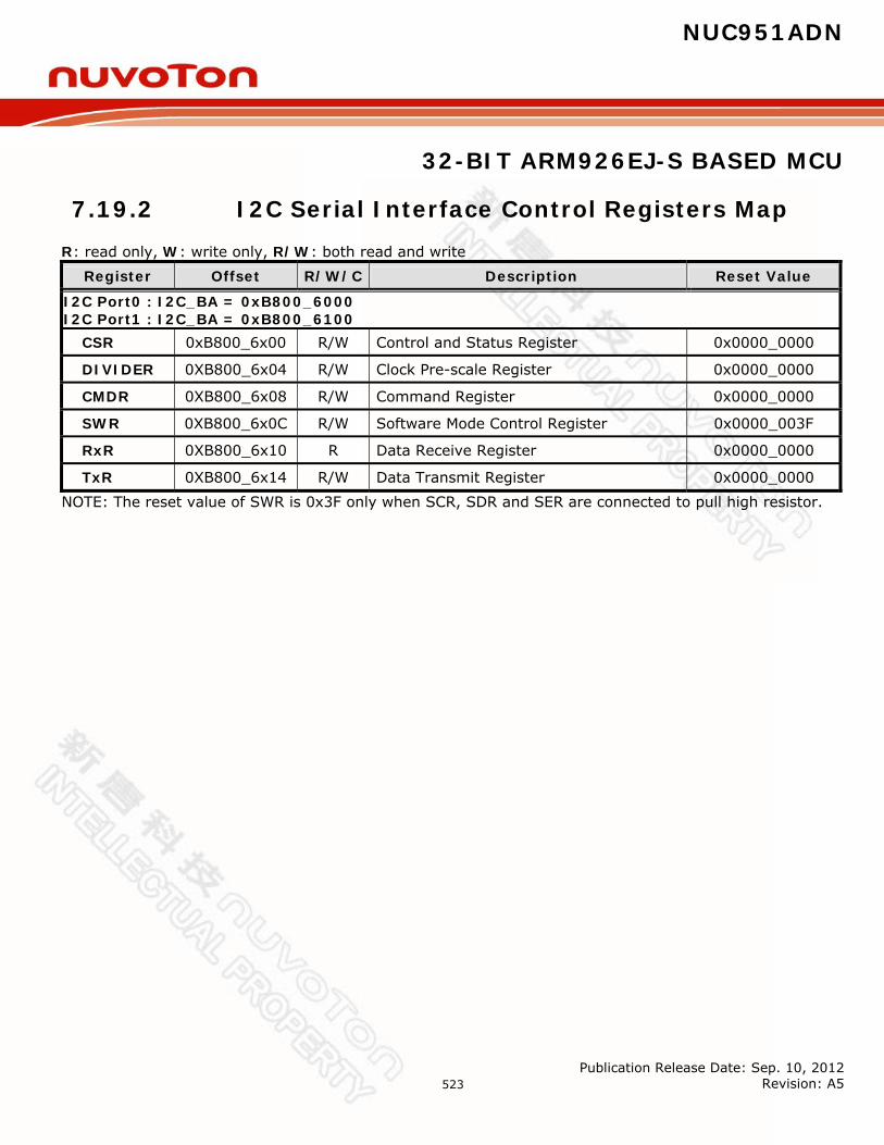
NUC951ADN
32-BIT ARM926EJ-S BASED MCU
Publication Release Date: Sep. 10, 2012 Revision: A5
523
7.19.2 I2C Serial Interface Control Registers Map R: read only, W: write only, R/W: both read and write
Register Offset R/W/C Description Reset Value
I2C Port0 : I2C_BA = 0xB800_6000 I2C Port1 : I2C_BA = 0xB800_6100
CSR 0xB800_6x00 R/W Control and Status Register 0x0000_0000
DIVIDER 0XB800_6x04 R/W Clock Pre-scale Register 0x0000_0000
CMDR 0XB800_6x08 R/W Command Register 0x0000_0000
SWR 0XB800_6x0C R/W Software Mode Control Register 0x0000_003F
RxR 0XB800_6x10 R Data Receive Register 0x0000_0000
TxR 0XB800_6x14 R/W Data Transmit Register 0x0000_0000 NOTE: The reset value of SWR is 0x3F only when SCR, SDR and SER are connected to pull high resistor.
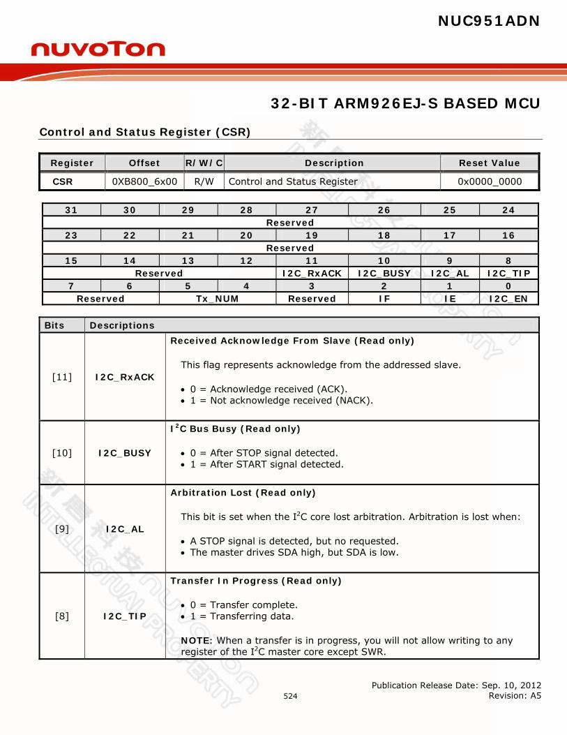
NUC951ADN
32-BIT ARM926EJ-S BASED MCU
Publication Release Date: Sep. 10, 2012 Revision: A5
524
Control and Status Register (CSR)
Register Offset R/W/C Description Reset Value
CSR 0XB800_6x00 R/W Control and Status Register 0x0000_0000
31 30 29 28 27 26 25 24 Reserved
23 22 21 20 19 18 17 16 Reserved
15 14 13 12 11 10 9 8 Reserved I2C_RxACK I2C_BUSY I2C_AL I2C_TIP
7 6 5 4 3 2 1 0 Reserved Tx_NUM Reserved IF IE I2C_EN
Bits Descriptions
[11] I2C_RxACK
Received Acknowledge From Slave (Read only)
This flag represents acknowledge from the addressed slave.
0 = Acknowledge received (ACK). 1 = Not acknowledge received (NACK).
[10] I2C_BUSY
I2C Bus Busy (Read only)
0 = After STOP signal detected. 1 = After START signal detected.
[9] I2C_AL
Arbitration Lost (Read only)
This bit is set when the I2C core lost arbitration. Arbitration is lost when:
A STOP signal is detected, but no requested. The master drives SDA high, but SDA is low.
[8] I2C_TIP
Transfer In Progress (Read only)
0 = Transfer complete. 1 = Transferring data.
NOTE: When a transfer is in progress, you will not allow writing to any register of the I2C master core except SWR.
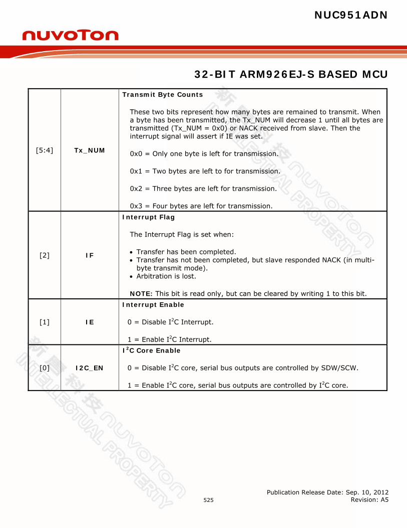
NUC951ADN
32-BIT ARM926EJ-S BASED MCU
Publication Release Date: Sep. 10, 2012 Revision: A5
525
[5:4] Tx_NUM
Transmit Byte Counts
These two bits represent how many bytes are remained to transmit. When a byte has been transmitted, the Tx_NUM will decrease 1 until all bytes are transmitted (Tx_NUM = 0x0) or NACK received from slave. Then the interrupt signal will assert if IE was set.
0x0 = Only one byte is left for transmission.
0x1 = Two bytes are left to for transmission.
0x2 = Three bytes are left for transmission.
0x3 = Four bytes are left for transmission.
[2] IF
Interrupt Flag
The Interrupt Flag is set when:
Transfer has been completed. Transfer has not been completed, but slave responded NACK (in multi-
byte transmit mode). Arbitration is lost.
NOTE: This bit is read only, but can be cleared by writing 1 to this bit.
[1] IE
Interrupt Enable
0 = Disable I2C Interrupt.
1 = Enable I2C Interrupt.
[0] I2C_EN
I2C Core Enable
0 = Disable I2C core, serial bus outputs are controlled by SDW/SCW.
1 = Enable I2C core, serial bus outputs are controlled by I2C core.

NUC951ADN
32-BIT ARM926EJ-S BASED MCU
Publication Release Date: Sep. 10, 2012 Revision: A5
526
Pre-scale Register (DIVIDER)
Register Offset R/W/C Description Reset Value
DIVIDER 0XB800_6x04 R/W Clock Pre-scale Register 0x0000_0000
31 30 29 28 27 26 25 24 Reserved
23 22 21 20 19 18 17 16 Reserved
15 14 13 12 11 10 9 8 DIVIDER[15:8]
7 6 5 4 3 2 1 0 DIVIDER[7:0]
Bits Descriptions
[15:0] DIVIDER
Clock Pre-scale Register It is used to pre-scale the SCL clock line. Due to the structure of the I2C interface, the core uses a 5*SCL clock internally. The pre-scale register must be programmed to this 5*SCL frequency (minus 1). Change the value of the pre-scale register only when the “I2C_EN” bit is cleared. Example: pclk = 32MHz, desired SCL = 100KHz
)(3)(6311005
32hexFdec
KHz
MHzprescale

NUC951ADN
32-BIT ARM926EJ-S BASED MCU
Publication Release Date: Sep. 10, 2012 Revision: A5
527
Command Register (CMDR)
Register Offset R/W/C Description Reset Value
CMDR 0XB800_6x08 R/W Command Register 0x0000_0000
31 30 29 28 27 26 25 24
Reserved
23 22 21 20 19 18 17 16
Reserved
15 14 13 12 11 10 9 8
Reserved
7 6 5 4 3 2 1 0
Reserved START STOP READ WRITE ACK NOTE: Software can write this register only when I2C_EN = 1. Bits Descriptions
[4] START Generate Start Condition
Generate (repeated) start condition on I2C bus.
[3] STOP Generate Stop Condition
Generate stop condition on I2C bus.
[2] READ Read Data From Slave
Retrieve data from slave.
[1] WRITE Write Data To Slave
Transmit data to slave.
[0] ACK
Send Acknowledge To Slave
When I2C behaves as a receiver, sent ACK (ACK = ‘0’) or NACK (ACK = ‘1’) to slave.
NOTE: The START, STOP, READ and WRITE bits are cleared automatically while transfer finished. READ and WRITE cannot be set concurrently.

NUC951ADN
32-BIT ARM926EJ-S BASED MCU
Publication Release Date: Sep. 10, 2012 Revision: A5
528
Software Mode Register (SWR)
Register Offset R/W/C Description Reset Value
SWR 0XB800_6x0C R/W Software Mode Control Register 0x0000_003F
31 30 29 28 27 26 25 24
Reserved
23 22 21 20 19 18 17 16
Reserved
15 14 13 12 11 10 9 8
Reserved
7 6 5 4 3 2 1 0
Reserved SER SDR SCR SEW SDW SCW NOTE: This register is used as software mode of I2C. Software can read/write this register no matter I2C_EN is 0 or 1. But SCL and SDA are controlled by software only when I2C_EN = 0. Bits Descriptions
[5] SER Serial Interface SDO Status (Read only) 0 = SDO is Low. 1 = SDO is High.
[4] SDR Serial Interface SDA Status (Read only) 0 = SDA is Low. 1 = SDA is High.
[3] SCR Serial Interface SCK Status (Read only) 0 = SCL is Low. 1 = SCL is High.
[2] SEW Serial Interface SDO Output Control 0 = SDO pin is driven Low. 1 = SDO pin is tri-state.
[1] SDW Serial Interface SDA Output Control 0 = SDA pin is driven Low. 1 = SDA pin is tri-state.
[0] SCW Serial Interface SCK Output Control 0 = SCL pin is driven Low. 1 = SCL pin is tri-state.
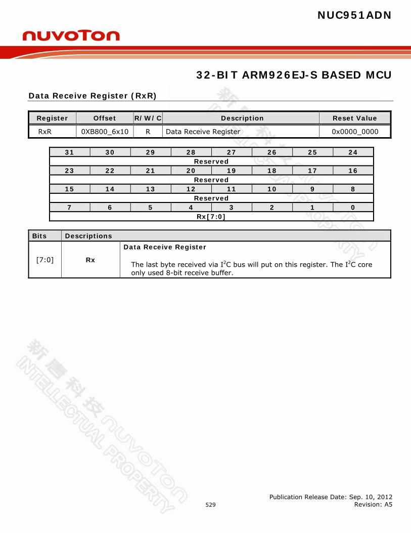
NUC951ADN
32-BIT ARM926EJ-S BASED MCU
Publication Release Date: Sep. 10, 2012 Revision: A5
529
Data Receive Register (RxR)
Register Offset R/W/C Description Reset Value
RxR 0XB800_6x10 R Data Receive Register 0x0000_0000
31 30 29 28 27 26 25 24 Reserved
23 22 21 20 19 18 17 16 Reserved
15 14 13 12 11 10 9 8 Reserved
7 6 5 4 3 2 1 0 Rx [7:0]
Bits Descriptions
[7:0] Rx
Data Receive Register
The last byte received via I2C bus will put on this register. The I2C core only used 8-bit receive buffer.
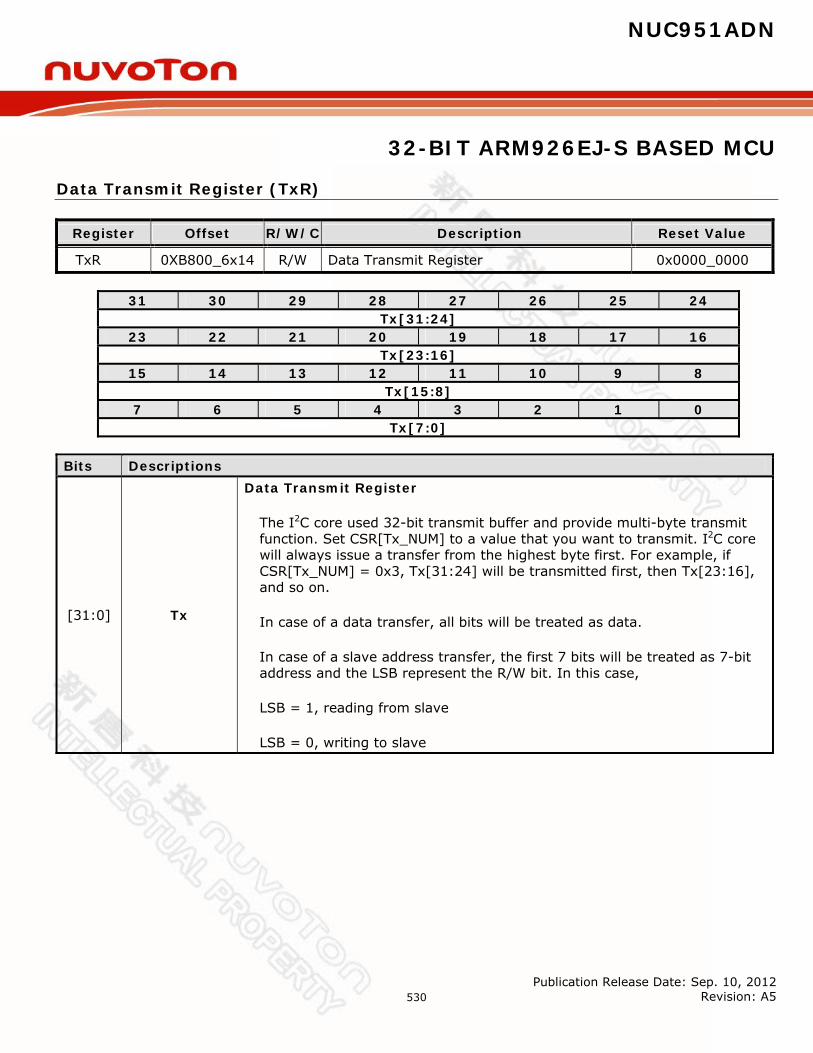
NUC951ADN
32-BIT ARM926EJ-S BASED MCU
Publication Release Date: Sep. 10, 2012 Revision: A5
530
Data Transmit Register (TxR)
Register Offset R/W/C Description Reset Value
TxR 0XB800_6x14 R/W Data Transmit Register 0x0000_0000
31 30 29 28 27 26 25 24 Tx [31:24]
23 22 21 20 19 18 17 16 Tx [23:16]
15 14 13 12 11 10 9 8 Tx [15:8]
7 6 5 4 3 2 1 0 Tx [7:0]
Bits Descriptions
[31:0] Tx
Data Transmit Register
The I2C core used 32-bit transmit buffer and provide multi-byte transmit function. Set CSR[Tx_NUM] to a value that you want to transmit. I2C core will always issue a transfer from the highest byte first. For example, if CSR[Tx_NUM] = 0x3, Tx[31:24] will be transmitted first, then Tx[23:16], and so on.
In case of a data transfer, all bits will be treated as data.
In case of a slave address transfer, the first 7 bits will be treated as 7-bit address and the LSB represent the R/W bit. In this case,
LSB = 1, reading from slave
LSB = 0, writing to slave
NUC951ADN
32-BIT ARM926EJ-S BASED MCU
Publication Release Date: Sep. 10, 2012 Revision: A5
531
7.20 Universal Serial Interface Controller (USI) The USI is a synchronous serial interface performs a serial-to-parallel conversion on data characters received from the peripheral, and a parallel-to-serial conversion on data characters received from CPU. This interface can drive up to 2 external peripherals and is seen as the master. It can generate an interrupt signal when data transfer is finished and can be cleared by writing 1 to the interrupt flag. The active level of device/slave select signal can be chosen to low active or high active, which depends on the peripheral it’s connected. Writing a divisor into DIVIDER register can program the frequency of serial clock output. This master core contains four 32-bit transmit/receive buffers, and can provide burst mode operation. The maximum bits can be transmitted/received is 32 bits, and can transmit/receive data up to four times successive. The USI (MICROWIRE/SPI) Master Core includes the following features:
Support MICROWIRE/SPI master mode
Full duplex synchronous serial data transfer
Variable length of transfer word up to 32 bits
Provide burst mode operation, transmit/receive can be executed up to four times in one transfer
MSB or LSB first data transfer
Rx and Tx on both rising and falling edge of serial clock independently
2 slave/device select lines
Fully static synchronous design with one clock domain
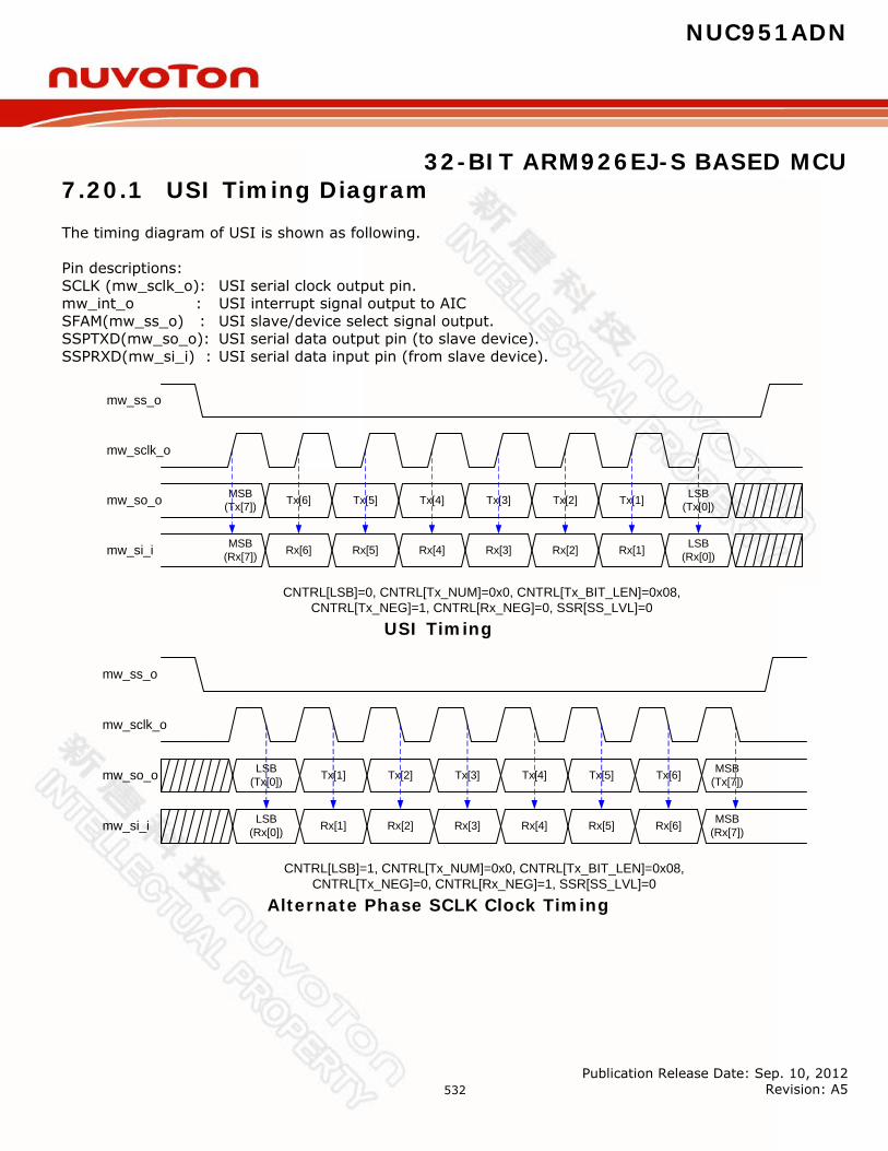
NUC951ADN
32-BIT ARM926EJ-S BASED MCU
Publication Release Date: Sep. 10, 2012 Revision: A5
532
7.20.1 USI Timing Diagram The timing diagram of USI is shown as following. Pin descriptions: SCLK (mw_sclk_o): USI serial clock output pin. mw_int_o : USI interrupt signal output to AIC SFAM(mw_ss_o) : USI slave/device select signal output. SSPTXD(mw_so_o): USI serial data output pin (to slave device). SSPRXD(mw_si_i) : USI serial data input pin (from slave device).
MSB(Tx[7])
LSB(Tx[0])
MSB(Rx[7])
LSB(Rx[0])
mw_ss_o
mw_sclk_o
mw_so_o
mw_si_i
CNTRL[LSB]=0, CNTRL[Tx_NUM]=0x0, CNTRL[Tx_BIT_LEN]=0x08,CNTRL[Tx_NEG]=1, CNTRL[Rx_NEG]=0, SSR[SS_LVL]=0
Tx[6] Tx[5] Tx[4] Tx[3] Tx[2] Tx[1]
Rx[6] Rx[5] Rx[4] Rx[3] Rx[2] Rx[1]
USI Timing
mw_ss_o
mw_sclk_o
mw_so_o
mw_si_i
CNTRL[LSB]=1, CNTRL[Tx_NUM]=0x0, CNTRL[Tx_BIT_LEN]=0x08,CNTRL[Tx_NEG]=0, CNTRL[Rx_NEG]=1, SSR[SS_LVL]=0
MSB(Tx[7])
LSB(Tx[0])
MSB(Rx[7])
LSB(Rx[0])
Tx[1] Tx[2] Tx[3] Tx[4] Tx[5] Tx[6]
Rx[1] Rx[2] Rx[3] Rx[4] Rx[5] Rx[6]
Alternate Phase SCLK Clock Timing

NUC951ADN
32-BIT ARM926EJ-S BASED MCU
Publication Release Date: Sep. 10, 2012 Revision: A5
533
7.20.2 USI Control Registers Map R: read only, W: write only, R/W: both read and write
Register Offset R/W Description Reset Value
USI_BA = 0xB800_6200
CNTRL 0xB800_6200 R/W Control and Status Register 0x0000_0004
DIVIDER 0xB800_6204 R/W Clock Divider Register 0x0000_0000
SSR 0xB800_6208 R/W Slave Select Register 0x0000_0000
Rx0 0xB800_6210 R Data Receive Register 0 0x0000_0000
Rx1 0xB800_6214 R Data Receive Register 1 0x0000_0000
Rx2 0xB800_6218 R Data Receive Register 2 0x0000_0000
Rx3 0xB800_621C R Data Receive Register 3 0x0000_0000
Tx0 0xB800_6210 W Data Transmit Register 0 0x0000_0000
Tx1 0xB800_6214 W Data Transmit Register 1 0x0000_0000
Tx2 0xB800_6218 W Data Transmit Register 2 0x0000_0000
Tx3 0xB800_621C W Data Transmit Register 3 0x0000_0000 NOTE 1: When software programs CNTRL, the GO_BUSY bit should be written last.
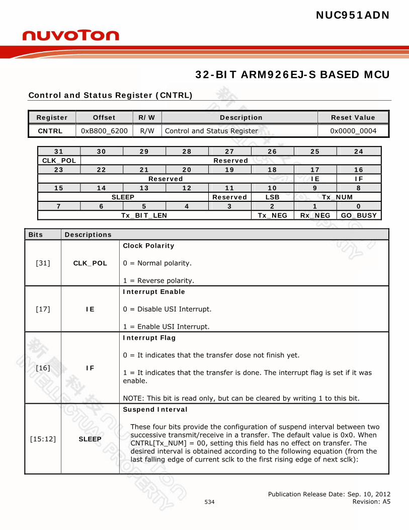
NUC951ADN
32-BIT ARM926EJ-S BASED MCU
Publication Release Date: Sep. 10, 2012 Revision: A5
534
Control and Status Register (CNTRL)
Register Offset R/W Description Reset Value
CNTRL 0xB800_6200 R/W Control and Status Register 0x0000_0004
31 30 29 28 27 26 25 24 CLK_POL Reserved
23 22 21 20 19 18 17 16 Reserved IE IF
15 14 13 12 11 10 9 8 SLEEP Reserved LSB Tx_NUM
7 6 5 4 3 2 1 0 Tx_BIT_LEN Tx_NEG Rx_NEG GO_BUSY
Bits Descriptions
[31] CLK_POL
Clock Polarity
0 = Normal polarity.
1 = Reverse polarity.
[17] IE
Interrupt Enable
0 = Disable USI Interrupt.
1 = Enable USI Interrupt.
[16] IF
Interrupt Flag
0 = It indicates that the transfer dose not finish yet.
1 = It indicates that the transfer is done. The interrupt flag is set if it was enable.
NOTE: This bit is read only, but can be cleared by writing 1 to this bit.
[15:12] SLEEP
Suspend Interval
These four bits provide the configuration of suspend interval between two successive transmit/receive in a transfer. The default value is 0x0. When CNTRL[Tx_NUM] = 00, setting this field has no effect on transfer. The desired interval is obtained according to the following equation (from the last falling edge of current sclk to the first rising edge of next sclk):
NUC951ADN
32-BIT ARM926EJ-S BASED MCU
Publication Release Date: Sep. 10, 2012 Revision: A5
535
(CNTRL[SLEEP] + 2)*period of SCLK
SLEEP = 0x0 … 2 SCLK clock cycle
……
SLEEP = 0xf … 17 SCLK clock cycle
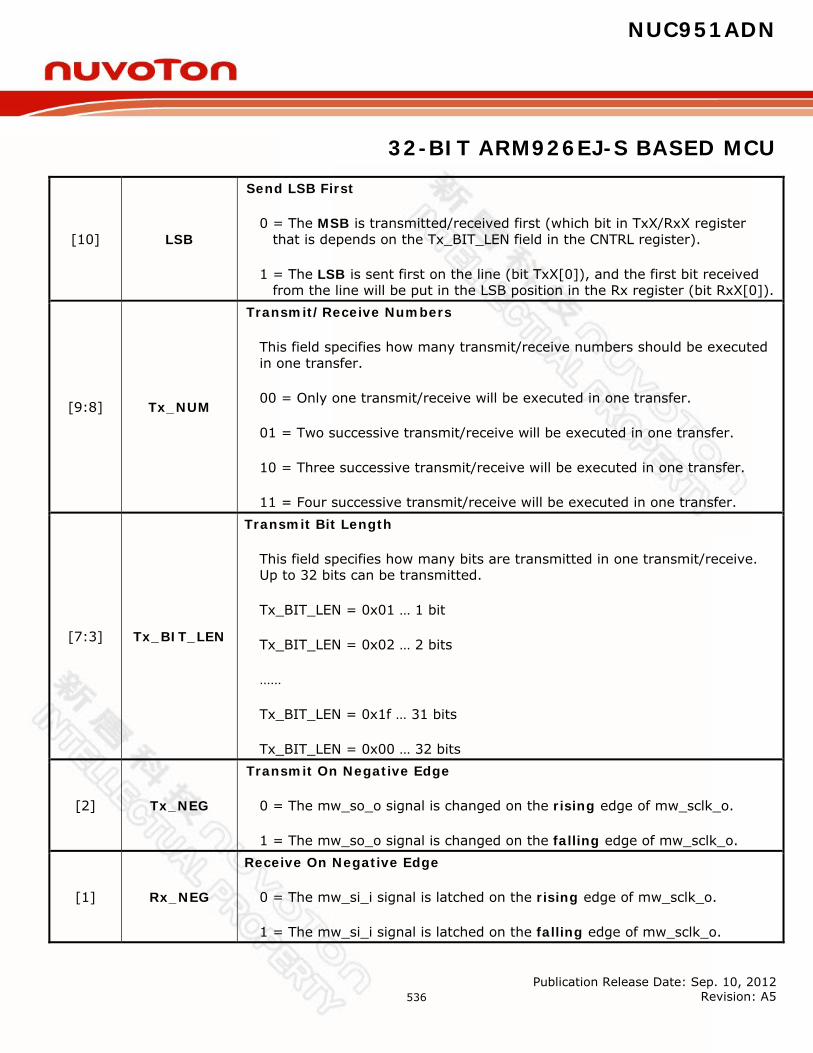
NUC951ADN
32-BIT ARM926EJ-S BASED MCU
Publication Release Date: Sep. 10, 2012 Revision: A5
536
[10] LSB
Send LSB First
0 = The MSB is transmitted/received first (which bit in TxX/RxX register that is depends on the Tx_BIT_LEN field in the CNTRL register).
1 = The LSB is sent first on the line (bit TxX[0]), and the first bit received from the line will be put in the LSB position in the Rx register (bit RxX[0]).
[9:8] Tx_NUM
Transmit/Receive Numbers
This field specifies how many transmit/receive numbers should be executed in one transfer.
00 = Only one transmit/receive will be executed in one transfer.
01 = Two successive transmit/receive will be executed in one transfer.
10 = Three successive transmit/receive will be executed in one transfer.
11 = Four successive transmit/receive will be executed in one transfer.
[7:3] Tx_BIT_LEN
Transmit Bit Length
This field specifies how many bits are transmitted in one transmit/receive. Up to 32 bits can be transmitted.
Tx_BIT_LEN = 0x01 … 1 bit
Tx_BIT_LEN = 0x02 … 2 bits
……
Tx_BIT_LEN = 0x1f … 31 bits
Tx_BIT_LEN = 0x00 … 32 bits
[2] Tx_NEG
Transmit On Negative Edge
0 = The mw_so_o signal is changed on the rising edge of mw_sclk_o.
1 = The mw_so_o signal is changed on the falling edge of mw_sclk_o.
[1] Rx_NEG
Receive On Negative Edge
0 = The mw_si_i signal is latched on the rising edge of mw_sclk_o.
1 = The mw_si_i signal is latched on the falling edge of mw_sclk_o.
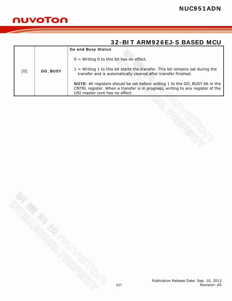
NUC951ADN
32-BIT ARM926EJ-S BASED MCU
Publication Release Date: Sep. 10, 2012 Revision: A5
537
[0] GO_BUSY
Go and Busy Status
0 = Writing 0 to this bit has no effect.
1 = Writing 1 to this bit starts the transfer. This bit remains set during the transfer and is automatically cleared after transfer finished.
NOTE: All registers should be set before writing 1 to the GO_BUSY bit in the CNTRL register. When a transfer is in progress, writing to any register of the USI master core has no effect.

NUC951ADN
32-BIT ARM926EJ-S BASED MCU
Publication Release Date: Sep. 10, 2012 Revision: A5
538
Divider Register (DIVIDER)
Register Offset R/W Description Reset Value
DIVIDER 0xB800_6204 R/W Clock Divider Register 0x0000_0000
31 30 29 28 27 26 25 24 Reserved
23 22 21 20 19 18 17 16 Reserved
15 14 13 12 11 10 9 8 DIVIDER[15:8]
7 6 5 4 3 2 1 0 DIVIDER[7:0]
Bits Descriptions
[15:0] DIVIDER
Clock Divider Register The value in this field is the frequency divider of the system clock pclk to generate the serial clock on the output mw_sclk_o. The desired frequency is obtained according to the following equation:
2*1
DIVIDER
ff pclk
sclk
NOTE: Suggest DIVIDER should be at least 1.
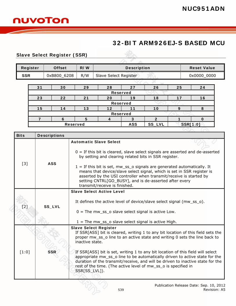
NUC951ADN
32-BIT ARM926EJ-S BASED MCU
Publication Release Date: Sep. 10, 2012 Revision: A5
539
Slave Select Register (SSR)
Register Offset R/W Description Reset Value
SSR 0xB800_6208 R/W Slave Select Register 0x0000_0000
31 30 29 28 27 26 25 24 Reserved
23 22 21 20 19 18 17 16 Reserved
15 14 13 12 11 10 9 8 Reserved
7 6 5 4 3 2 1 0 Reserved ASS SS_LVL SSR[1:0]
Bits Descriptions
[3] ASS
Automatic Slave Select
0 = If this bit is cleared, slave select signals are asserted and de-asserted by setting and clearing related bits in SSR register.
1 = If this bit is set, mw_ss_o signals are generated automatically. It means that device/slave select signal, which is set in SSR register is asserted by the USI controller when transmit/receive is started by setting CNTRL[GO_BUSY], and is de-asserted after every transmit/receive is finished.
[2] SS_LVL
Slave Select Active Level
It defines the active level of device/slave select signal (mw_ss_o).
0 = The mw_ss_o slave select signal is active Low.
1 = The mw_ss_o slave select signal is active High.
[1:0] SSR
Slave Select Register If SSR[ASS] bit is cleared, writing 1 to any bit location of this field sets the proper mw_ss_o line to an active state and writing 0 sets the line back to inactive state.
If SSR[ASS] bit is set, writing 1 to any bit location of this field will select appropriate mw_ss_o line to be automatically driven to active state for the duration of the transmit/receive, and will be driven to inactive state for the rest of the time. (The active level of mw_ss_o is specified in SSR[SS_LVL]).
NUC951ADN
32-BIT ARM926EJ-S BASED MCU
Publication Release Date: Sep. 10, 2012 Revision: A5
540
NOTE: This interface can only drive one device/slave at a given time. Therefore, the SSR of the selected device must be set to its active level before starting any read or write transfer.
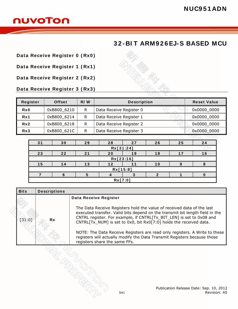
NUC951ADN
32-BIT ARM926EJ-S BASED MCU
Publication Release Date: Sep. 10, 2012 Revision: A5
541
Data Receive Register 0 (Rx0)
Data Receive Register 1 (Rx1)
Data Receive Register 2 (Rx2)
Data Receive Register 3 (Rx3)
Register Offset R/W Description Reset Value
Rx0 0xB800_6210 R Data Receive Register 0 0x0000_0000
Rx1 0xB800_6214 R Data Receive Register 1 0x0000_0000
Rx2 0xB800_6218 R Data Receive Register 2 0x0000_0000
Rx3 0xB800_621C R Data Receive Register 3 0x0000_0000
31 30 29 28 27 26 25 24 Rx [31:24]
23 22 21 20 19 18 17 16 Rx [23:16]
15 14 13 12 11 10 9 8 Rx [15:8]
7 6 5 4 3 2 1 0 Rx [7:0]
Bits Descriptions
[31:0] Rx
Data Receive Register
The Data Receive Registers hold the value of received data of the last executed transfer. Valid bits depend on the transmit bit length field in the CNTRL register. For example, if CNTRL[Tx_BIT_LEN] is set to 0x08 and CNTRL[Tx_NUM] is set to 0x0, bit Rx0[7:0] holds the received data.
NOTE: The Data Receive Registers are read only registers. A Write to these registers will actually modify the Data Transmit Registers because those registers share the same FFs.

NUC951ADN
32-BIT ARM926EJ-S BASED MCU
Publication Release Date: Sep. 10, 2012 Revision: A5
542
Data Transmit Register 0 (Tx0)
Data Transmit Register 1 (Tx1)
Data Transmit Register 2 (Tx2)
Data Transmit Register 3 (Tx3)
Register Offset R/W Description Reset Value
Tx0 0xB800_6210 W Data Transmit Register 0 0x0000_0000
Tx1 0xB800_6214 W Data Transmit Register 1 0x0000_0000
Tx2 0xB800_6218 W Data Transmit Register 2 0x0000_0000
Tx3 0xB800_621C W Data Transmit Register 3 0x0000_0000
31 30 29 28 27 26 25 24 Tx [31:24]
23 22 21 20 19 18 17 16 Tx [23:16]
15 14 13 12 11 10 9 8 Tx [15:8]
7 6 5 4 3 2 1 0 Tx [7:0]
Bits Descriptions
[31:0] Tx
Data Transmit Register
The Data Transmit Registers hold the data to be transmitted in the next transfer. Valid bits depend on the transmit bit length field in the CNTRL register. For example, if CNTRL[Tx_BIT_LEN] is set to 0x08 and the CNTRL[Tx_NUM] is set to 0x0, the bit Tx0[7:0] will be transmitted in next transfer. If CNTRL[Tx_BIT_LEN] is set to 0x00 and CNTRL[Tx_NUM] is set to 0x3, the core will perform four 32-bit transmit/receive successive using the same setting (the order is Tx0[31:0], Tx1[31:0], Tx2[31:0], Tx3[31:0]).
NOTE: The RxX and TxX registers share the same flip-flops, which mean that what is received from the input data line in one transfer will be transmitted on the output data line in the next transfer if no write access to the TxX register is executed between the transfers.
NUC951ADN
32-BIT ARM926EJ-S BASED MCU
Publication Release Date: Sep. 10, 2012 Revision: A5
543
7.21 Pulse Width Modulation (PWM) This Controller includes 4 channels PWM Timers. They can be divided into two groups. Each group has 1 Pre-scalar, 1 clock divider, 2 clock selectors, 2 16-bit counters, 2 16-bit comparators, 1 Dead-Zone generator. They are all driven by APB system clock in chip. Each channel can be used as a timer and issue interrupt independently. Two channels PWM Timers in one group share the same pre-scalar. Clock divider provides each channel with 5 clock sources (1, 1/2, 1/4, 1/8, 1/16). Each channel receives its own clock signal from clock divider which receives clock from 8-bit pre-scalar. The 16-bit counter in each channel receive clock signal from clock selector and can be used to handle one PWM period. The 16-bit comparator compares number in counter with threshold number in register loaded previously to generate PWM duty cycle. The clock signal from clock divider is called PWM clock. Dead-Zone generator utilize PWM clock as clock source. Once Dead-Zone generator is enabled, output of two PWM timers in one group is blocked. Two output pin are all used as Dead-Zone generator output signal to control off-chip power device. To prevent PWM driving output pin with unsteady waveform, 16-bit counter and 16-bit comparator are implemented with double buffering feature. User can feel free to write data to counter buffer register and comparator buffer register without generating glitch. When 16-bit down counter reaches zero, the interrupt request is generated to inform CPU that time is up. When counter reaches zero, if counter is set as toggle mode, it is reloaded automatically and start to generate next cycle. User can set counter as one-shot mode instead of toggle mode. If counter is set as one-shot mode, counter will stop and generate one interrupt request when it reaches zero. The value of comparator is used for pulse width modulation. The counter control logic changes the output level when down-counter value matches the value of compare register. The PWM Timer features are shown as below: Two 8-bit pre-scalars and two clock dividers Four clock selectors Four 16-bit counters and four 16-bit comparators Two Dead-Zone generator
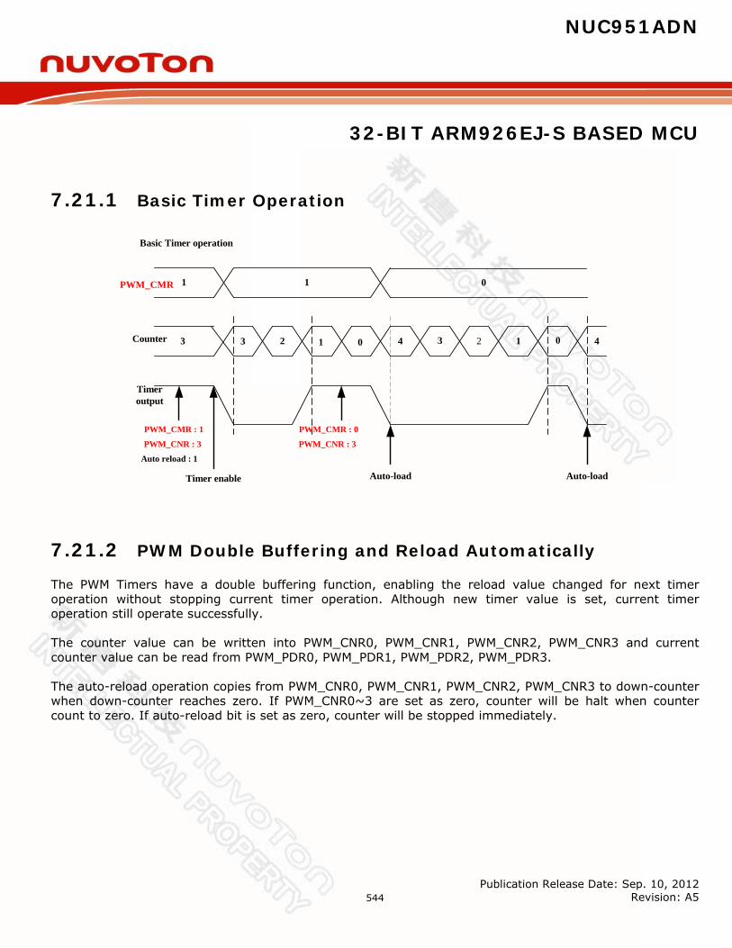
NUC951ADN
32-BIT ARM926EJ-S BASED MCU
Publication Release Date: Sep. 10, 2012 Revision: A5
544
7.21.1 Basic Timer Operation
Basic Timer operation
PWM_CMR 1 0
Counter 3 3 2 1 0 4 3 2 1 0 4
Timeroutput
1
PWM_CMR : 1
PWM_CNR : 3
Auto reload : 1
Timer enable
PWM_CMR : 0
PWM_CNR : 3
Auto-load Auto-load
7.21.2 PWM Double Buffering and Reload Automatically
The PWM Timers have a double buffering function, enabling the reload value changed for next timer operation without stopping current timer operation. Although new timer value is set, current timer operation still operate successfully. The counter value can be written into PWM_CNR0, PWM_CNR1, PWM_CNR2, PWM_CNR3 and current counter value can be read from PWM_PDR0, PWM_PDR1, PWM_PDR2, PWM_PDR3. The auto-reload operation copies from PWM_CNR0, PWM_CNR1, PWM_CNR2, PWM_CNR3 to down-counter when down-counter reaches zero. If PWM_CNR0~3 are set as zero, counter will be halt when counter count to zero. If auto-reload bit is set as zero, counter will be stopped immediately.

NUC951ADN
32-BIT ARM926EJ-S BASED MCU
Publication Release Date: Sep. 10, 2012 Revision: A5
545
pwm_out
write a nonzeronumber to prescaler &
setup clock dividor
Start
PWM_CNR=150PWM_CMR=50
151
51
200
50
PWM_CNR=199PWM_CMR=49
PWM_CNR=99PWM_CMR=0
100
1
PWM_CNR=0PWM_CMR=XX
Stop
PWM double buffering
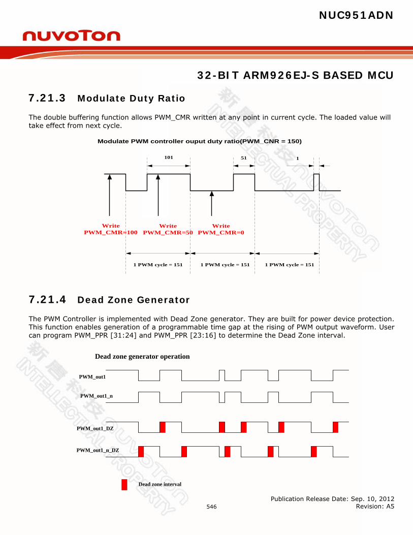
NUC951ADN
32-BIT ARM926EJ-S BASED MCU
Publication Release Date: Sep. 10, 2012 Revision: A5
546
7.21.3 Modulate Duty Ratio
The double buffering function allows PWM_CMR written at any point in current cycle. The loaded value will take effect from next cycle.
Modulate PWM controller ouput duty ratio(PWM_CNR = 150)
WritePWM_CMR=100
WritePWM_CMR=50
WritePWM_CMR=0
1 PWM cycle = 151 1 PWM cycle = 151 1 PWM cycle = 151
101 51 1
7.21.4 Dead Zone Generator
The PWM Controller is implemented with Dead Zone generator. They are built for power device protection. This function enables generation of a programmable time gap at the rising of PWM output waveform. User can program PWM_PPR [31:24] and PWM_PPR [23:16] to determine the Dead Zone interval.
Dead zone generator operation
PWM_out1
PWM_out1_n
PWM_out1_DZ
PWM_out1_n_DZ
Dead zone interval
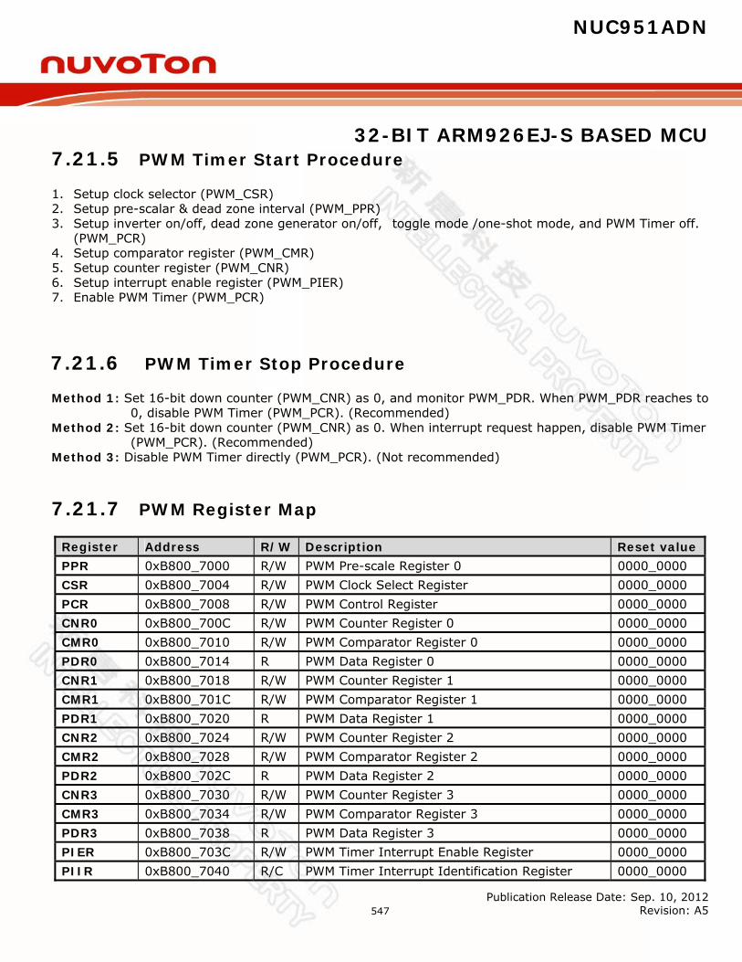
NUC951ADN
32-BIT ARM926EJ-S BASED MCU
Publication Release Date: Sep. 10, 2012 Revision: A5
547
7.21.5 PWM Timer Start Procedure
1. Setup clock selector (PWM_CSR) 2. Setup pre-scalar & dead zone interval (PWM_PPR) 3. Setup inverter on/off, dead zone generator on/off, toggle mode /one-shot mode, and PWM Timer off.
(PWM_PCR) 4. Setup comparator register (PWM_CMR) 5. Setup counter register (PWM_CNR) 6. Setup interrupt enable register (PWM_PIER) 7. Enable PWM Timer (PWM_PCR)
7.21.6 PWM Timer Stop Procedure
Method 1: Set 16-bit down counter (PWM_CNR) as 0, and monitor PWM_PDR. When PWM_PDR reaches to 0, disable PWM Timer (PWM_PCR). (Recommended)
Method 2: Set 16-bit down counter (PWM_CNR) as 0. When interrupt request happen, disable PWM Timer (PWM_PCR). (Recommended)
Method 3: Disable PWM Timer directly (PWM_PCR). (Not recommended)
7.21.7 PWM Register Map
Register Address R/W Description Reset value PPR 0xB800_7000 R/W PWM Pre-scale Register 0 0000_0000 CSR 0xB800_7004 R/W PWM Clock Select Register 0000_0000 PCR 0xB800_7008 R/W PWM Control Register 0000_0000 CNR0 0xB800_700C R/W PWM Counter Register 0 0000_0000 CMR0 0xB800_7010 R/W PWM Comparator Register 0 0000_0000 PDR0 0xB800_7014 R PWM Data Register 0 0000_0000 CNR1 0xB800_7018 R/W PWM Counter Register 1 0000_0000 CMR1 0xB800_701C R/W PWM Comparator Register 1 0000_0000 PDR1 0xB800_7020 R PWM Data Register 1 0000_0000 CNR2 0xB800_7024 R/W PWM Counter Register 2 0000_0000 CMR2 0xB800_7028 R/W PWM Comparator Register 2 0000_0000 PDR2 0xB800_702C R PWM Data Register 2 0000_0000 CNR3 0xB800_7030 R/W PWM Counter Register 3 0000_0000 CMR3 0xB800_7034 R/W PWM Comparator Register 3 0000_0000 PDR3 0xB800_7038 R PWM Data Register 3 0000_0000 PIER 0xB800_703C R/W PWM Timer Interrupt Enable Register 0000_0000 PIIR 0xB800_7040 R/C PWM Timer Interrupt Identification Register 0000_0000
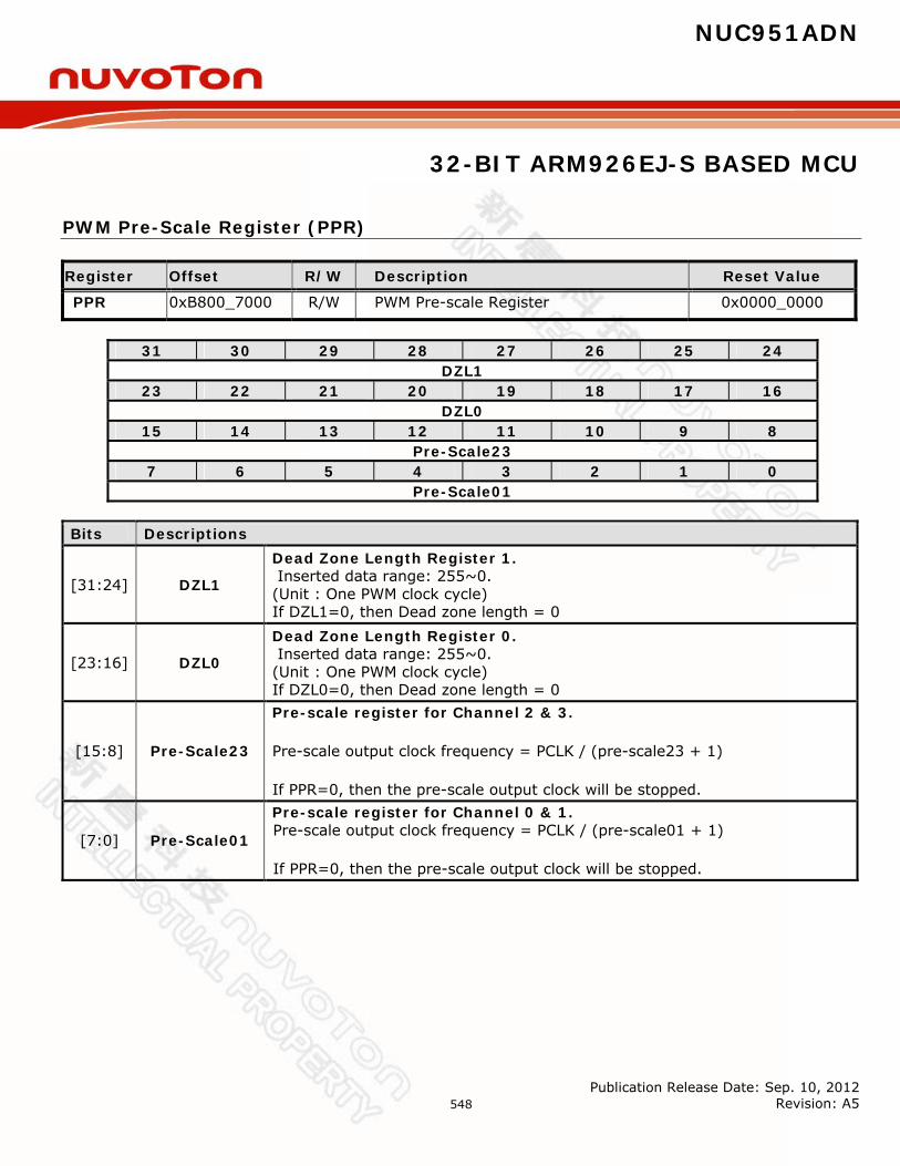
NUC951ADN
32-BIT ARM926EJ-S BASED MCU
Publication Release Date: Sep. 10, 2012 Revision: A5
548
PWM Pre-Scale Register (PPR)
Register Offset R/W Description Reset Value
PPR 0xB800_7000 R/W PWM Pre-scale Register 0x0000_0000
31 30 29 28 27 26 25 24
DZL1 23 22 21 20 19 18 17 16
DZL0 15 14 13 12 11 10 9 8
Pre-Scale23 7 6 5 4 3 2 1 0
Pre-Scale01 Bits Descriptions
[31:24] DZL1
Dead Zone Length Register 1. Inserted data range: 255~0. (Unit : One PWM clock cycle) If DZL1=0, then Dead zone length = 0
[23:16] DZL0
Dead Zone Length Register 0. Inserted data range: 255~0. (Unit : One PWM clock cycle) If DZL0=0, then Dead zone length = 0
[15:8] Pre-Scale23
Pre-scale register for Channel 2 & 3.
Pre-scale output clock frequency = PCLK / (pre-scale23 + 1)
If PPR=0, then the pre-scale output clock will be stopped.
[7:0] Pre-Scale01
Pre-scale register for Channel 0 & 1. Pre-scale output clock frequency = PCLK / (pre-scale01 + 1)
If PPR=0, then the pre-scale output clock will be stopped.
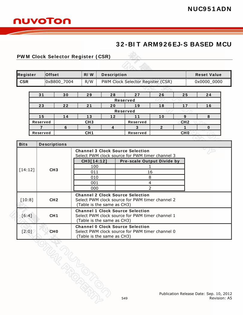
NUC951ADN
32-BIT ARM926EJ-S BASED MCU
Publication Release Date: Sep. 10, 2012 Revision: A5
549
PWM Clock Selector Register (CSR)
Register Offset R/W Description Reset Value
CSR 0xB800_7004 R/W PWM Clock Selector Register (CSR) 0x0000_0000
31 30 29 28 27 26 25 24
Reserved 23 22 21 20 19 18 17 16
Reserved 15 14 13 12 11 10 9 8
Reserved CH3 Reserved CH2 7 6 5 4 3 2 1 0
Reserved CH1 Reserved CH0 Bits Descriptions
[14:12] CH3
Channel 3 Clock Source Selection Select PWM clock source for PWM timer channel 3
CH3[14:12] Pre-scale Output Divide by 100 1 011 16 010 8 001 4 000 2
[10:8] CH2 Channel 2 Clock Source Selection Select PWM clock source for PWM timer channel 2 (Table is the same as CH3)
[6:4] CH1 Channel 1 Clock Source Selection Select PWM clock source for PWM timer channel 1 (Table is the same as CH3)
[2:0] CH0 Channel 0 Clock Source Selection Select PWM clock source for PWM timer channel 0 (Table is the same as CH3)
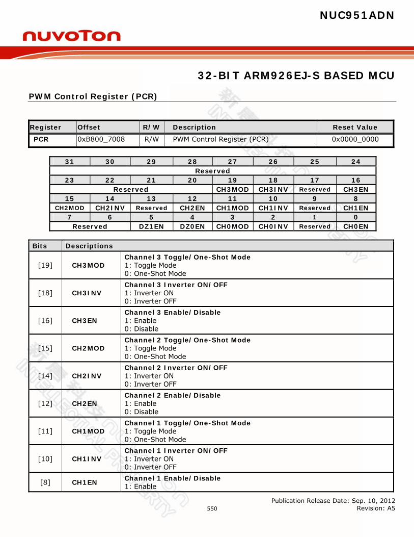
NUC951ADN
32-BIT ARM926EJ-S BASED MCU
Publication Release Date: Sep. 10, 2012 Revision: A5
550
PWM Control Register (PCR)
Register Offset R/W Description Reset Value
PCR 0xB800_7008 R/W PWM Control Register (PCR) 0x0000_0000
31 30 29 28 27 26 25 24
Reserved 23 22 21 20 19 18 17 16
Reserved CH3MOD CH3INV Reserved CH3EN 15 14 13 12 11 10 9 8
CH2MOD CH2INV Reserved CH2EN CH1MOD CH1INV Reserved CH1EN 7 6 5 4 3 2 1 0
Reserved DZ1EN DZ0EN CH0MOD CH0INV Reserved CH0EN Bits Descriptions
[19] CH3MOD Channel 3 Toggle/One-Shot Mode 1: Toggle Mode 0: One-Shot Mode
[18] CH3INV Channel 3 Inverter ON/OFF 1: Inverter ON 0: Inverter OFF
[16] CH3EN Channel 3 Enable/Disable 1: Enable 0: Disable
[15] CH2MOD Channel 2 Toggle/One-Shot Mode 1: Toggle Mode 0: One-Shot Mode
[14] CH2INV Channel 2 Inverter ON/OFF 1: Inverter ON 0: Inverter OFF
[12] CH2EN Channel 2 Enable/Disable 1: Enable 0: Disable
[11] CH1MOD Channel 1 Toggle/One-Shot Mode 1: Toggle Mode 0: One-Shot Mode
[10] CH1INV Channel 1 Inverter ON/OFF 1: Inverter ON 0: Inverter OFF
[8] CH1EN Channel 1 Enable/Disable 1: Enable
NUC951ADN
32-BIT ARM926EJ-S BASED MCU
Publication Release Date: Sep. 10, 2012 Revision: A5
551
0: Disable
[5] DZ1EN Dead-Zone 1 Generator Enable/Disable 1: Enable 0: Disable
[4] DZ0EN Dead-Zone 0 Generator Enable/Disable 1: Enable 0: Disable
[3] CH0MOD Channel 0 Toggle/One-Shot Mode 1: Toggle Mode 0: One-Shot Mode
[2] CH0INV Channel 0 Inverter ON/OFF 1: Inverter ON 0: Inverter OFF
[0] CH0EN Channel 0 Enable/Disable 1: Enable 0: Disable

NUC951ADN
32-BIT ARM926EJ-S BASED MCU
Publication Release Date: Sep. 10, 2012 Revision: A5
552
PWM Counter Register 3-0 (CNR3-0)
Register Offset R/W Description Reset Value
CNR0 0xB800_700C R/W PWM Counter Register 0 0x0000_0000
CNR1 0xB800_7018 R/W PWM Counter Register 1 0x0000_0000
CNR2 0xB800_7024 R/W PWM Counter Register 2 0x0000_0000
CNR3 0xB800_7030 R/W PWM Counter Register 3 0x0000_0000
31 30 29 28 27 26 25 24
Reserved 23 22 21 20 19 18 17 16
Reserved 15 14 13 12 11 10 9 8
CNR 7 6 5 4 3 2 1 0
CNR Bits Descriptions
[15:0] CNR
PWM Counter/Timer Loaded Value Inserted data range : 65535~0 (Unit : 1 PWM clock cycle) Note 1: One PWM cycle width = CNR + 1. If CNR equal zero, PWM counter/timer will be stopped. Note 2: Programmer can feel free to write a data to CNR at any time, and it will take effect in next cycle.
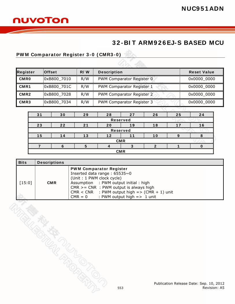
NUC951ADN
32-BIT ARM926EJ-S BASED MCU
Publication Release Date: Sep. 10, 2012 Revision: A5
553
PWM Comparator Register 3-0 (CMR3-0)
Register Offset R/W Description Reset Value
CMR0 0xB800_7010 R/W PWM Comparator Register 0 0x0000_0000
CMR1 0xB800_701C R/W PWM Comparator Register 1 0x0000_0000
CMR2 0xB800_7028 R/W PWM Comparator Register 2 0x0000_0000
CMR3 0xB800_7034 R/W PWM Comparator Register 3 0x0000_0000
31 30 29 28 27 26 25 24
Reserved 23 22 21 20 19 18 17 16
Reserved 15 14 13 12 11 10 9 8
CMR 7 6 5 4 3 2 1 0
CMR Bits Descriptions
[15:0] CMR
PWM Comparator Register Inserted data range : 65535~0 (Unit : 1 PWM clock cycle) Assumption : PWM output initial : high CMR >= CNR : PWM output is always high CMR < CNR : PWM output high => (CMR + 1) unit CMR = 0 : PWM output high => 1 unit

NUC951ADN
32-BIT ARM926EJ-S BASED MCU
Publication Release Date: Sep. 10, 2012 Revision: A5
554
PWM Data Register 3-0 (PDR 3-0)
Register Offset R/W Description Reset Value
PDR0 0xB800_7014 R PWM Data Register 0 0x0000_0000
PDR1 0xB800_7020 R PWM Data Register 1 0x0000_0000
PDR2 0xB800_702C R PWM Data Register 2 0x0000_0000
PDR3 0xB800_7038 R PWM Data Register 3 0x0000_0000
31 30 29 28 27 26 25 24 Reserved
23 22 21 20 19 18 17 16 Reserved
15 14 13 12 11 10 9 8 PDR
7 6 5 4 3 2 1 0 PDR
Bits Descriptions
[15:0] PDR PWM Data Register PDR means the PWM counter number.
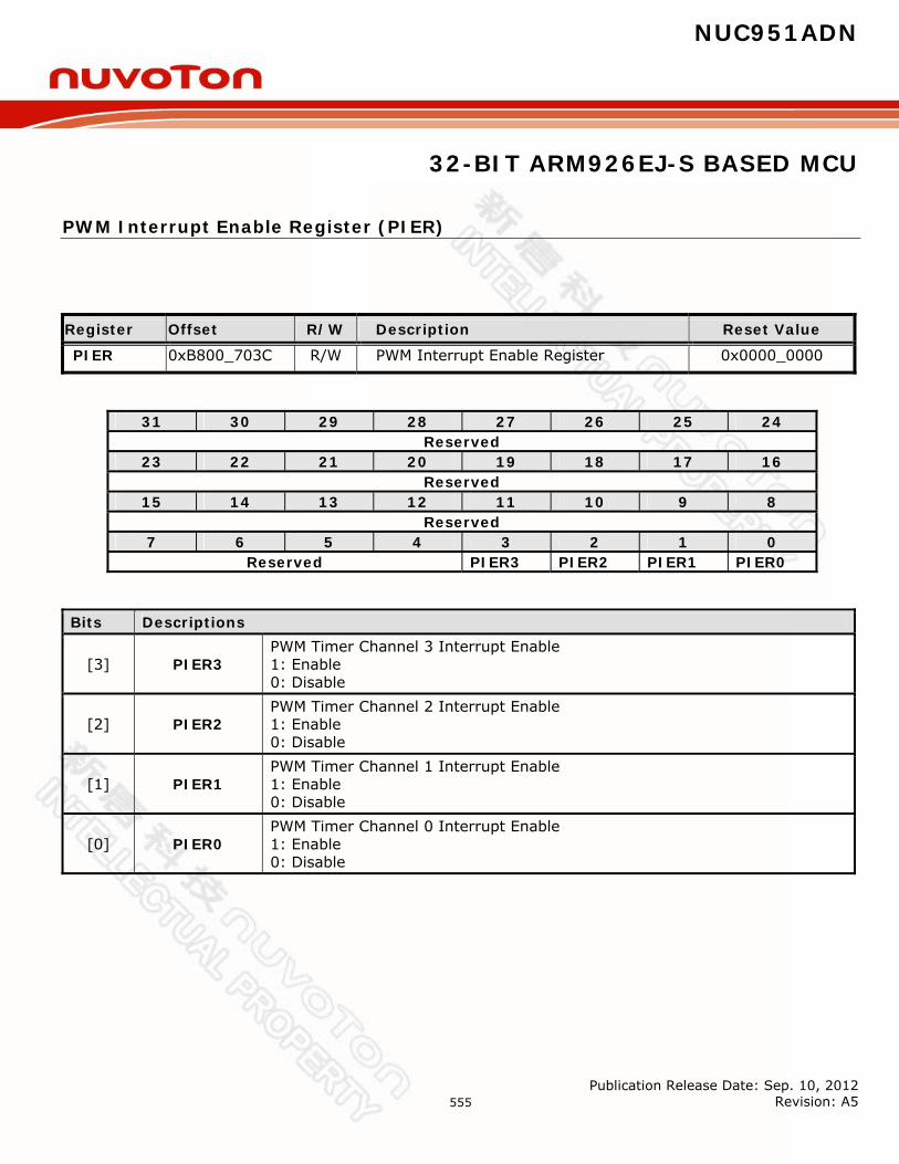
NUC951ADN
32-BIT ARM926EJ-S BASED MCU
Publication Release Date: Sep. 10, 2012 Revision: A5
555
PWM Interrupt Enable Register (PIER)
Register Offset R/W Description Reset Value
PIER 0xB800_703C R/W PWM Interrupt Enable Register 0x0000_0000
31 30 29 28 27 26 25 24 Reserved
23 22 21 20 19 18 17 16 Reserved
15 14 13 12 11 10 9 8 Reserved
7 6 5 4 3 2 1 0 Reserved PIER3 PIER2 PIER1 PIER0
Bits Descriptions
[3] PIER3 PWM Timer Channel 3 Interrupt Enable 1: Enable 0: Disable
[2] PIER2 PWM Timer Channel 2 Interrupt Enable 1: Enable 0: Disable
[1] PIER1 PWM Timer Channel 1 Interrupt Enable 1: Enable 0: Disable
[0] PIER0 PWM Timer Channel 0 Interrupt Enable 1: Enable 0: Disable
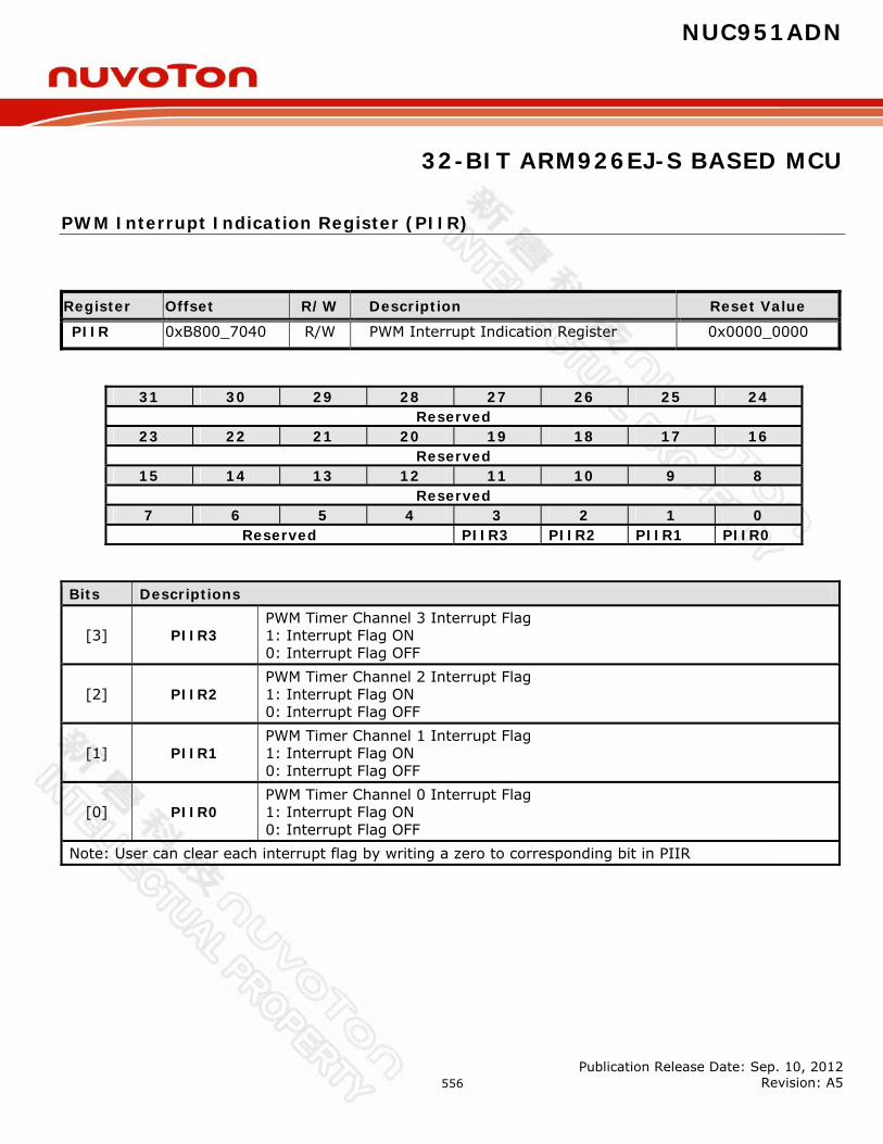
NUC951ADN
32-BIT ARM926EJ-S BASED MCU
Publication Release Date: Sep. 10, 2012 Revision: A5
556
PWM Interrupt Indication Register (PIIR)
Register Offset R/W Description Reset Value
PIIR 0xB800_7040 R/W PWM Interrupt Indication Register 0x0000_0000
31 30 29 28 27 26 25 24 Reserved
23 22 21 20 19 18 17 16 Reserved
15 14 13 12 11 10 9 8 Reserved
7 6 5 4 3 2 1 0 Reserved PIIR3 PIIR2 PIIR1 PIIR0
Bits Descriptions
[3] PIIR3 PWM Timer Channel 3 Interrupt Flag 1: Interrupt Flag ON 0: Interrupt Flag OFF
[2] PIIR2 PWM Timer Channel 2 Interrupt Flag 1: Interrupt Flag ON 0: Interrupt Flag OFF
[1] PIIR1 PWM Timer Channel 1 Interrupt Flag 1: Interrupt Flag ON 0: Interrupt Flag OFF
[0] PIIR0 PWM Timer Channel 0 Interrupt Flag 1: Interrupt Flag ON 0: Interrupt Flag OFF
Note: User can clear each interrupt flag by writing a zero to corresponding bit in PIIR

NUC951ADN
32-BIT ARM926EJ-S BASED MCU
Publication Release Date: Sep. 10, 2012 Revision: A5
557
7.22 Keypad Interface (KPI)
The Keypad Interface (KPI) is an APB slave with 4-row scan output and 8-column scan input. KPI scans an array up to 16x8 with an external 4 to 16 decoder. It can also be programmed to scan 8x8 or 4x8 key array. If the 4x8 array is selected then external decoder is not necessary because the scan signals are driven by chip itself. Any 1 or 2 keys in the array that pressed are de-bounced and encoded. If more than 2 keys are pressed, only the keys or apparent keys in the array with the lowest address will be decoded. The KPI supports 2-keys scan interrupt and specified 3-keys interrupt or chip reset. If the 3 pressed keys matches with the 3 keys defined in KPI3KCONF, it will generate an interrupt or chip reset to nWDOG reset output depend on the ENRST setting. The interrupt is generated whenever the scanner detects a key is pressed and then after the key is released. The interrupt conditions are 1 key, or 2 keys and no keys. This chip provides two keypad connecting interface. One is allocated in GPIOC interface, the other is in GPIOI interface. Software should set KPSEL bit in KPICONF register to decide which interface is used as keypad connection port. The keypad interface has the following features: maximum 16x8 array with an external 4 to 16 decoder programmable de-bounce time low-power wakeup function supported only for 4x8 array programmable three-key reset
Keypad Interface

NUC951ADN
32-BIT ARM926EJ-S BASED MCU
Publication Release Date: Sep. 10, 2012 Revision: A5
558
7.22.1 Keypad Interface Register Map
Register Address R/W Description Reset Value KPI_BA = 0xB800_8000 KPICONF 0xB800_8000 R/W Keypad controller configuration Register 0x0000_0000 KPI3KCONF 0xB800_8004 R/W Keypad controller 3-keys configuration register 0x0000_0000 KPILPCONF 0xB800_8008 R/W Keypad controller low power configuration register 0x0000_0000 KPISTATUS 0xB800_800C R Keypad controller status register 0x0000_0000
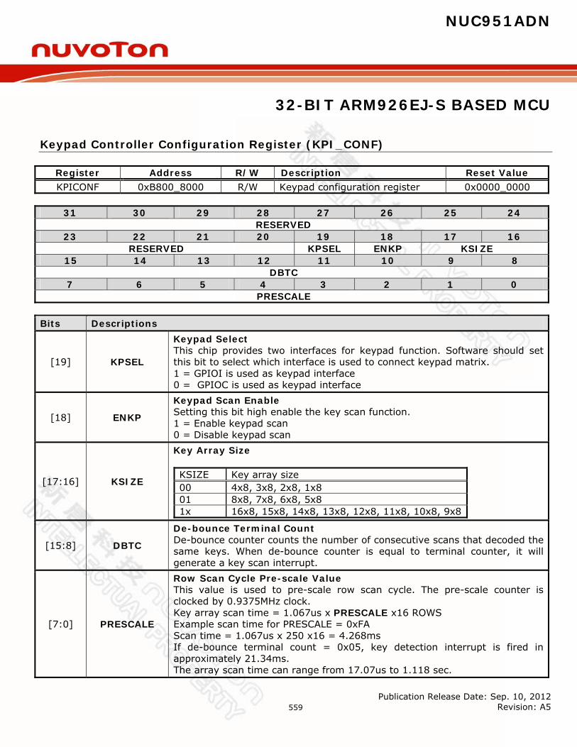
NUC951ADN
32-BIT ARM926EJ-S BASED MCU
Publication Release Date: Sep. 10, 2012 Revision: A5
559
Keypad Controller Configuration Register (KPI_CONF)
Register Address R/W Description Reset Value KPICONF 0xB800_8000 R/W Keypad configuration register 0x0000_0000
31 30 29 28 27 26 25 24
RESERVED 23 22 21 20 19 18 17 16
RESERVED KPSEL ENKP KSIZE 15 14 13 12 11 10 9 8
DBTC 7 6 5 4 3 2 1 0
PRESCALE Bits Descriptions
[19] KPSEL
Keypad Select This chip provides two interfaces for keypad function. Software should set this bit to select which interface is used to connect keypad matrix. 1 = GPIOI is used as keypad interface 0 = GPIOC is used as keypad interface
[18] ENKP
Keypad Scan Enable Setting this bit high enable the key scan function. 1 = Enable keypad scan 0 = Disable keypad scan
[17:16] KSIZE
Key Array Size KSIZE Key array size 00 4x8, 3x8, 2x8, 1x8 01 8x8, 7x8, 6x8, 5x8 1x 16x8, 15x8, 14x8, 13x8, 12x8, 11x8, 10x8, 9x8
[15:8] DBTC
De-bounce Terminal Count De-bounce counter counts the number of consecutive scans that decoded the same keys. When de-bounce counter is equal to terminal counter, it will generate a key scan interrupt.
[7:0] PRESCALE
Row Scan Cycle Pre-scale Value This value is used to pre-scale row scan cycle. The pre-scale counter is clocked by 0.9375MHz clock. Key array scan time = 1.067us x PRESCALE x16 ROWS Example scan time for PRESCALE = 0xFA Scan time = 1.067us x 250 x16 = 4.268ms If de-bounce terminal count = 0x05, key detection interrupt is fired in approximately 21.34ms. The array scan time can range from 17.07us to 1.118 sec.

NUC951ADN
32-BIT ARM926EJ-S BASED MCU
Publication Release Date: Sep. 10, 2012 Revision: A5
560
Keypad Controller 3-keys configuration Register (KPI3KCONF)
Register Address R/W Description Reset Value
KPI3KCONF 0xB800_8004 W/R Three-key configuration register 0x0000_0000
31 30 29 28 27 26 25 24 EN3KY ENRST
23 22 21 20 19 18 17 16 RESERVED K32R K32C
15 14 13 12 11 10 9 8 RESERVED K31R K31C
7 6 5 4 3 2 1 0 RESERVED K30R K30C Bits Descriptions
[25] EN3KY Enable Three-keys Detection Setting this bit enables hardware to detect 3 keys specified by software
[24] ENRST
Enable Three-key Reset Setting this bit enable hardware reset when three-key is detected
EN3KY ENRST Function 0 x Three-key function is disable 1 0 Generate three-key interrupt 1 1 Hardware reset by three-key-reset
[22:19] K32R The #3 Key Row Address [18:16] K32C The #3 Key Column Address [14:11] K31R The #2 Key Row Address [10:8] K31C The #2 Key Column Address [6:3] K30R The #1 Key Row Address [2:0] K30C The #1 Key Column Address

NUC951ADN
32-BIT ARM926EJ-S BASED MCU
Publication Release Date: Sep. 10, 2012 Revision: A5
561
Keypad Interface Low Power Mode Configuration Register (KPILPCONF)
Register Address R/W Description Reset Value
KPILPCOF 0xB800_8008 W/R Low power configuration register 0x0000_0000
31 30 29 28 27 26 25 24 RESERVED
23 22 21 20 19 18 17 16 RESERVED WAKE
15 14 13 12 11 10 9 8 LPWCEN
7 6 5 4 3 2 1 0 RESERVED LPWR
Bits Descriptions
[16] WAKE
Lower Power Wakeup Enable Setting this bit enables low power wakeup 1 = Wakeup enable 0 = Not enable
[15:8] LPWCEN Low Power Wakeup Column Enable Enable column[7:0] low power wakeup
[3:0] LPWR Low Power Wakeup Row Address Define the row address keys used to wakeup

NUC951ADN
32-BIT ARM926EJ-S BASED MCU
Publication Release Date: Sep. 10, 2012 Revision: A5
562
Key Pad Interface Status Register (KPISTATUS)
Register Address R/W Description Reset Value KPISTATUS 0xB800_800C R/O key pad status register 0x0000_0000
31 30 29 28 27 26 25 24
RESERVED 23 22 21 20 19 18 17 16
INT 3 K R S T PDWAKE 3KEY 2KEY 1KEY 15 14 13 12 11 10 9 8
RESERVED KEY1R KEY1C 7 6 5 4 3 2 1 0
RESERVED KEY0R KEY0C Bits Descriptions
[21] INT Key Interrupt This bit indicates the key scan interrupt is active and that one or two keys have changed status.
[20] 3KRST
3-Keys Reset Flag This bit will be set after 3-keys reset occur. 1 = 3 keys reset 0 = Not reset
[19] PDWAKE
Power Down Wakeup Flag This flag indicates the chip is wakeup from power down by keypad 1 = Wakeup up by keypad 0 = Not wakeup
[17] 2KEY Double-key Press This bit indicates that 2 keys have been detected.
[16] 1KEY Single-key Press This bit indicates that 1 key has been detected.
[14:11] KEY1R KEY1 Row Address This value indicates key1 row address
[10:8] KEY1C KEY1 Column Address This value indicates key1 column address
[6:3] KEY0R KEY0 Row Address This value indicates key0 row address
[2:0] KEY0C KEY0 Column Address This value indicates key0 column address.
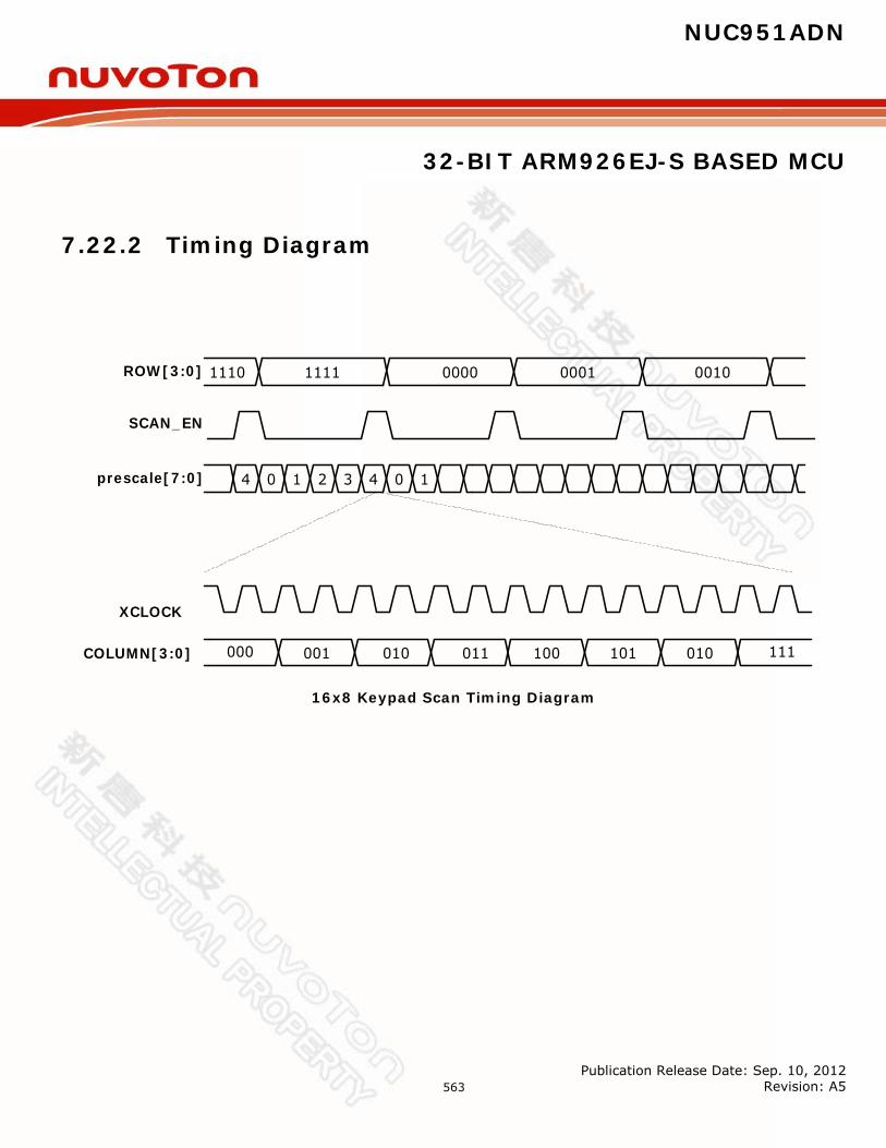
NUC951ADN
32-BIT ARM926EJ-S BASED MCU
Publication Release Date: Sep. 10, 2012 Revision: A5
563
7.22.2 Timing Diagram
ROW[3:0]
prescale[7:0]
1110 1111 0000
COLUMN[3:0] 000 001 010 111010 011 100 101
0 1 2 3 4 0 14
0001 0010
SCAN_EN
XCLOCK
16x8 Keypad Scan Timing Diagram
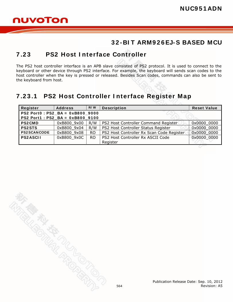
NUC951ADN
32-BIT ARM926EJ-S BASED MCU
Publication Release Date: Sep. 10, 2012 Revision: A5
564
7.23 PS2 Host Interface Controller The PS2 host controller interface is an APB slave consisted of PS2 protocol. It is used to connect to the keyboard or other device through PS2 interface. For example, the keyboard will sends scan codes to the host controller when the key is pressed or released. Besides Scan codes, commands can also be sent to the keyboard from host.
7.23.1 PS2 Host Controller Interface Register Map
Register Address R/W Description Reset Value PS2 Port0 : PS2_BA = 0xB800_9000 PS2 Port1 : PS2_BA = 0xB800_9100 PS2CMD 0xB800_9x00 R/W PS2 Host Controller Command Register 0x0000_0000 PS2STS 0xB800_9x04 R/W PS2 Host Controller Status Register 0x0000_0000 PS2SCANCODE 0xB800_9x08 RO PS2 Host Controller Rx Scan Code Register 0x0000_0000 PS2ASCII 0xB800_9x0C RO PS2 Host Controller Rx ASCII Code
Register 0x0000_0000
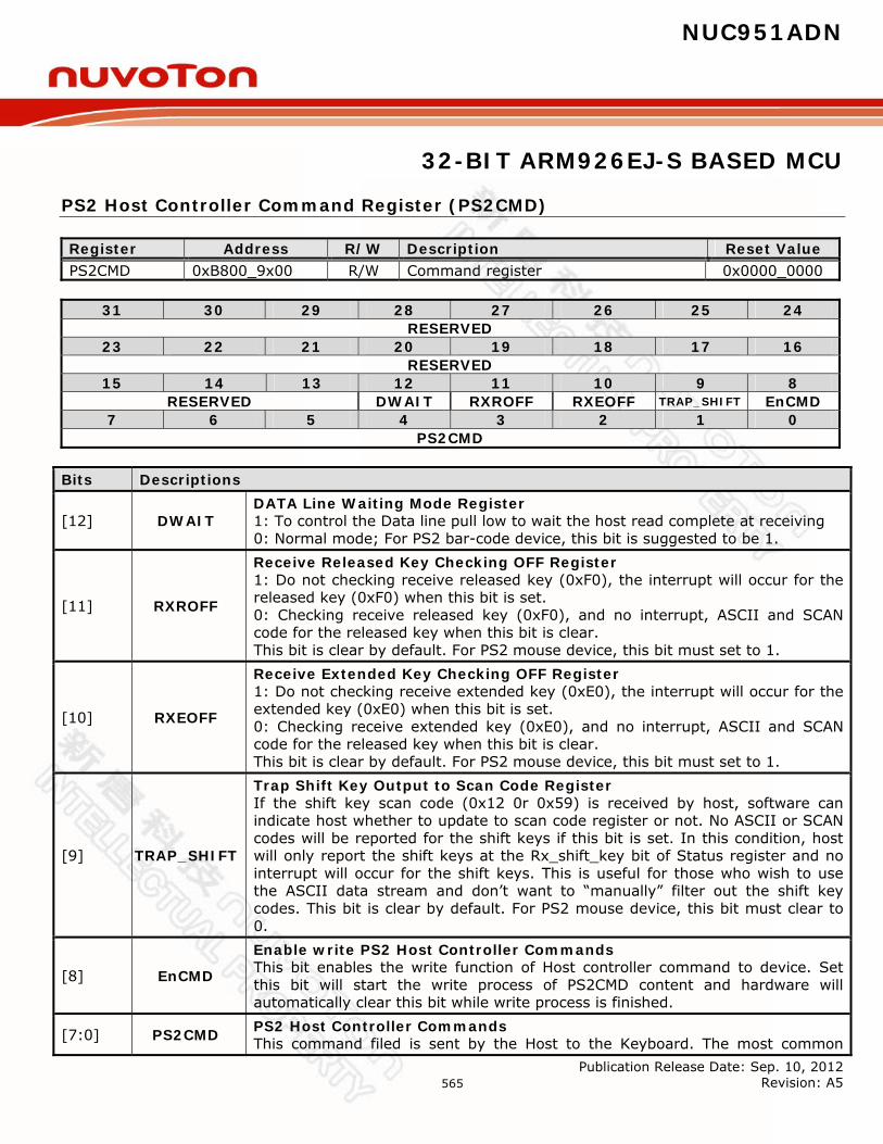
NUC951ADN
32-BIT ARM926EJ-S BASED MCU
Publication Release Date: Sep. 10, 2012 Revision: A5
565
PS2 Host Controller Command Register (PS2CMD)
Register Address R/W Description Reset Value PS2CMD 0xB800_9x00 R/W Command register 0x0000_0000
31 30 29 28 27 26 25 24
RESERVED 23 22 21 20 19 18 17 16
RESERVED 15 14 13 12 11 10 9 8
RESERVED DWAIT RXROFF RXEOFF TRAP_SHIFT EnCMD 7 6 5 4 3 2 1 0
PS2CMD Bits Descriptions
[12] DWAIT DATA Line Waiting Mode Register 1: To control the Data line pull low to wait the host read complete at receiving 0: Normal mode; For PS2 bar-code device, this bit is suggested to be 1.
[11] RXROFF
Receive Released Key Checking OFF Register 1: Do not checking receive released key (0xF0), the interrupt will occur for the released key (0xF0) when this bit is set. 0: Checking receive released key (0xF0), and no interrupt, ASCII and SCAN code for the released key when this bit is clear. This bit is clear by default. For PS2 mouse device, this bit must set to 1.
[10] RXEOFF
Receive Extended Key Checking OFF Register 1: Do not checking receive extended key (0xE0), the interrupt will occur for the extended key (0xE0) when this bit is set. 0: Checking receive extended key (0xE0), and no interrupt, ASCII and SCAN code for the released key when this bit is clear. This bit is clear by default. For PS2 mouse device, this bit must set to 1.
[9] TRAP_SHIFT
Trap Shift Key Output to Scan Code Register If the shift key scan code (0x12 0r 0x59) is received by host, software can indicate host whether to update to scan code register or not. No ASCII or SCAN codes will be reported for the shift keys if this bit is set. In this condition, host will only report the shift keys at the Rx_shift_key bit of Status register and no interrupt will occur for the shift keys. This is useful for those who wish to use the ASCII data stream and don’t want to “manually” filter out the shift key codes. This bit is clear by default. For PS2 mouse device, this bit must clear to 0.
[8] EnCMD
Enable write PS2 Host Controller Commands This bit enables the write function of Host controller command to device. Set this bit will start the write process of PS2CMD content and hardware will automatically clear this bit while write process is finished.
[7:0] PS2CMD PS2 Host Controller Commands This command filed is sent by the Host to the Keyboard. The most common

NUC951ADN
32-BIT ARM926EJ-S BASED MCU
Publication Release Date: Sep. 10, 2012 Revision: A5
566
command would be the setting/resetting of the Status Indicators (i.e. the Num lock, Caps Lock & Scroll Lock LEDs).

NUC951ADN
32-BIT ARM926EJ-S BASED MCU
Publication Release Date: Sep. 10, 2012 Revision: A5
567
PS2 Host Controller Status Register (PS2STS)
Register Address R/W Description Reset Value PS2STS 0xB800_9x04 R/W Status register 0x0000_0000
31 30 29 28 27 26 25 24
RESERVED 23 22 21 20 19 18 17 16
RESERVED 15 14 13 12 11 10 9 8
RESERVED 7 6 5 4 3 2 1 0
RESERVED Tx_err Tx_IRQ RESERVED Rx_2bytes Rx_IRQ
Bits Descriptions
[5] Tx_err
Transmit Error Status This bit indicates software that device doesn’t response ACK after Host wrote a command to it. This bit is valid when Tx_IRQ is asserted. It will automatically reset after software starts next command writing process. If software writes one to this bit, it also can be clear.
[4] Tx_IRQ
Transmit Complete Interrupt This bit indicates software that the process of Host controller writing command to device is finished. Software needs to write one to this bit to clear this interrupt.
[1] Rx_2bytes
Receive 2 Bytes Flag This bit indicates software that Host controller receives two byte data from device. The second data are stored at the high byte of PS2_SCANCODE register. This bit is valid when Rx_IRQ is asserted, and is read only.
[0] Rx_IRQ
Receive Interrupt This bit indicates software that Host controller receives one byte data from device. This data is stored at PS2_SCANCODE register. Software needs to write one to this bit to clear this interrupt after reading receiving data in Rx_SCAN_CODE register.
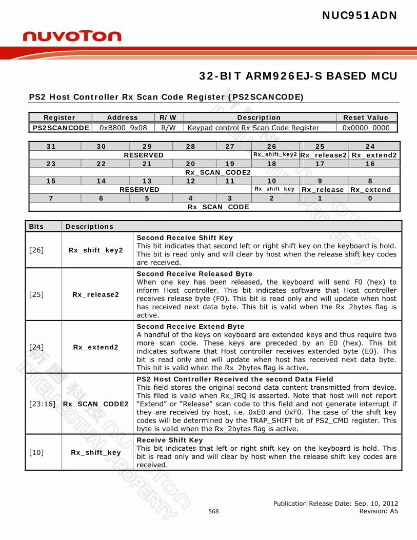
NUC951ADN
32-BIT ARM926EJ-S BASED MCU
Publication Release Date: Sep. 10, 2012 Revision: A5
568
PS2 Host Controller Rx Scan Code Register (PS2SCANCODE)
Register Address R/W Description Reset Value PS2SCANCODE 0xB800_9x08 R/W Keypad control Rx Scan Code Register 0x0000_0000
31 30 29 28 27 26 25 24
RESERVED Rx_shift_key2 Rx_release2 Rx_extend2 23 22 21 20 19 18 17 16
Rx_SCAN_CODE2 15 14 13 12 11 10 9 8
RESERVED Rx_shift_key Rx_release Rx_extend 7 6 5 4 3 2 1 0
Rx_SCAN_CODE Bits Descriptions
[26] Rx_shift_key2
Second Receive Shift Key This bit indicates that second left or right shift key on the keyboard is hold. This bit is read only and will clear by host when the release shift key codes are received.
[25] Rx_release2
Second Receive Released Byte When one key has been released, the keyboard will send F0 (hex) to inform Host controller. This bit indicates software that Host controller receives release byte (F0). This bit is read only and will update when host has received next data byte. This bit is valid when the Rx_2bytes flag is active.
[24] Rx_extend2
Second Receive Extend Byte A handful of the keys on keyboard are extended keys and thus require two more scan code. These keys are preceded by an E0 (hex). This bit indicates software that Host controller receives extended byte (E0). This bit is read only and will update when host has received next data byte. This bit is valid when the Rx_2bytes flag is active.
[23:16] Rx_SCAN_CODE2
PS2 Host Controller Received the second Data Field This field stores the original second data content transmitted from device. This filed is valid when Rx_IRQ is asserted. Note that host will not report “Extend” or “Release” scan code to this field and not generate interrupt if they are received by host, i.e. 0xE0 and 0xF0. The case of the shift key codes will be determined by the TRAP_SHIFT bit of PS2_CMD register. This byte is valid when the Rx_2bytes flag is active.
[10] Rx_shift_key
Receive Shift Key This bit indicates that left or right shift key on the keyboard is hold. This bit is read only and will clear by host when the release shift key codes are received.
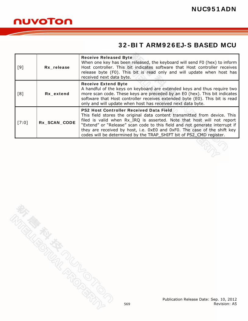
NUC951ADN
32-BIT ARM926EJ-S BASED MCU
Publication Release Date: Sep. 10, 2012 Revision: A5
569
[9] Rx_release
Receive Released Byte When one key has been released, the keyboard will send F0 (hex) to inform Host controller. This bit indicates software that Host controller receives release byte (F0). This bit is read only and will update when host has received next data byte.
[8] Rx_extend
Receive Extend Byte A handful of the keys on keyboard are extended keys and thus require two more scan code. These keys are preceded by an E0 (hex). This bit indicates software that Host controller receives extended byte (E0). This bit is read only and will update when host has received next data byte.
[7:0] Rx_SCAN_CODE
PS2 Host Controller Received Data Field This field stores the original data content transmitted from device. This filed is valid when Rx_IRQ is asserted. Note that host will not report “Extend” or “Release” scan code to this field and not generate interrupt if they are received by host, i.e. 0xE0 and 0xF0. The case of the shift key codes will be determined by the TRAP_SHIFT bit of PS2_CMD register.
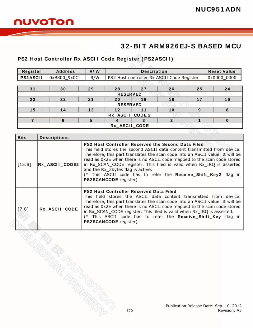
NUC951ADN
32-BIT ARM926EJ-S BASED MCU
Publication Release Date: Sep. 10, 2012 Revision: A5
570
PS2 Host Controller Rx ASCII Code Register (PS2ASCII)
Register Address R/W Description Reset Value PS2ASCII 0xB800_9x0C R/W PS2 Host controller Rx ASCII Code Register 0x0000_0000
31 30 29 28 27 26 25 24
RESERVED 23 22 21 20 19 18 17 16
RESERVED 15 14 13 12 11 10 9 8
Rx_ASCII_CODE 2 7 6 5 4 3 2 1 0
Rx_ASCII_CODE Bits Descriptions
[15:8] Rx_ASCII_CODE2
PS2 Host Controller Received the Second Data Filed This field stores the second ASCII data content transmitted from device. Therefore, this part translates the scan code into an ASCII value. It will be read as 0x2E when there is no ASCII code mapped to the scan code stored in Rx_SCAN_CODE register. This filed is valid when Rx_IRQ is asserted and the Rx_2bytes flag is active. (* This ASCII code has to refer the Receive_Shift_Key2 flag in PS2SCANCODE register)
[7:0] Rx_ASCII_CODE
PS2 Host Controller Received Data Filed This field stores the ASCII data content transmitted from device. Therefore, this part translates the scan code into an ASCII value. It will be read as 0x2E when there is no ASCII code mapped to the scan code stored in Rx_SCAN_CODE register. This filed is valid when Rx_IRQ is asserted. (* This ASCII code has to refer the Receive_Shift_Key flag in PS2SCANCODE register)

NUC951ADN
32-BIT ARM926EJ-S BASED MCU
Publication Release Date: Sep. 10, 2012 Revision: A5
571
8 Electrical Specifications
8.1 Absolute Maximum Ratings
Ambient temperature .................................……………............................ -40 C ~ 85 C
Storage temperature ..................................................…….................. -50 C ~ 125C
Voltage on any pin ...............................................................……........ -0.5V ~ 6V
Power supply voltage (Core logic) ..............................…...........………..…. -0.5V ~ 2.5V
Power supply voltage (IO Buffer) ...............................…...........………..…. -0.5V ~ 4.6V
Injection current (latch-up testing) ..............................................………. 100mA
Crystal Frequency ...............................................…...........………..………. 4MHz ~ 30MHz
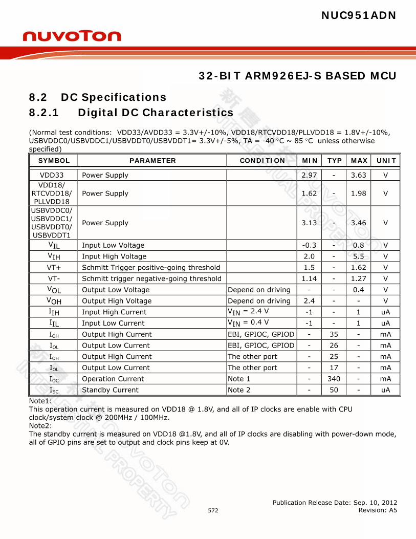
NUC951ADN
32-BIT ARM926EJ-S BASED MCU
Publication Release Date: Sep. 10, 2012 Revision: A5
572
8.2 DC Specifications 8.2.1 Digital DC Characteristics (Normal test conditions: VDD33/AVDD33 = 3.3V+/-10%, VDD18/RTCVDD18/PLLVDD18 = 1.8V+/-10%, USBVDDC0/USBVDDC1/USBVDDT0/USBVDDT1= 3.3V+/-5%, TA = -40 C ~ 85 C unless otherwise specified)
SYMBOL PARAMETER CONDITION MIN TYP MAX UNIT
VDD33 Power Supply 2.97 - 3.63 V VDD18/
RTCVDD18/ PLLVDD18
Power Supply 1.62 - 1.98 V
USBVDDC0/ USBVDDC1/ USBVDDT0/ USBVDDT1
Power Supply 3.13 - 3.46 V
VIL Input Low Voltage -0.3 - 0.8 V VIH Input High Voltage 2.0 - 5.5 V VT+ Schmitt Trigger positive-going threshold 1.5 - 1.62 V VT- Schmitt trigger negative-going threshold 1.14 - 1.27 V VOL Output Low Voltage Depend on driving - - 0.4 V VOH Output High Voltage Depend on driving 2.4 - - V IIH Input High Current VIN = 2.4 V -1 - 1 uA IIL Input Low Current VIN = 0.4 V -1 - 1 uA IOH Output High Current EBI, GPIOC, GPIOD - 35 - mA IOL Output Low Current EBI, GPIOC, GPIOD - 26 - mA IOH Output High Current The other port - 25 - mA IOL Output Low Current The other port - 17 - mA IOC Operation Current Note 1 - 340 - mA ISC Standby Current Note 2 - 50 - uA
Note1: This operation current is measured on VDD18 @ 1.8V, and all of IP clocks are enable with CPU clock/system clock @ 200MHz / 100MHz. Note2: The standby current is measured on VDD18 @1.8V, and all of IP clocks are disabling with power-down mode, all of GPIO pins are set to output and clock pins keep at 0V.
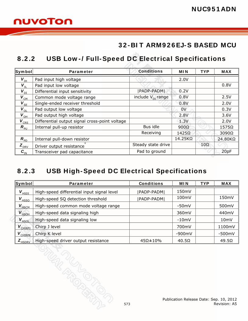
NUC951ADN
32-BIT ARM926EJ-S BASED MCU
Publication Release Date: Sep. 10, 2012 Revision: A5
573
8.2.2 USB Low-/Full-Speed DC Electrical Specifications
Symbol Parameter Conditions MIN TYP MAX
VIH Pad input high voltage 2.0V VIL Pad input low voltage 0.8V VDI Differential input sensitivity |PADP-PADM| 0.2V VCM Common mode voltage range include VDI range 0.8V 2.5V VSE Single-ended receiver threshold 0.8V 2.0V VOL Pad output low voltage 0V 0.3V VOH Pad output high voltage 2.8V 3.6V VCRS Differential output signal cross-point voltage 1.3V 2.0V RPU Internal pull-up resistor Bus idle 900Ω 1575Ω
Receiving 1425Ω 3090Ω RPD Internal pull-down resistor 14.25KΩ 24.80KΩ ZDRV Driver output resistance
‡ Steady state drive 10Ω
CIN Transceiver pad capacitance Pad to ground 20pF
8.2.3 USB High-Speed DC Electrical Specifications
Symbol Parameter Conditions MIN TYP MAX
VHSDI High-speed differential input signal level |PADP-PADM| 150mV
VHSSQ High-speed SQ detection threshold |PADP-PADM| 100mV 150mV
VHSCM High-speed common mode voltage range -50mV 500mV VHSOH High-speed data signaling high 360mV 440mV VHSOL High-speed data signaling low -10mV 10mV VCHIRPJ Chirp J level 700mV 1100mV VCHIRPK Chirp K level -900mV -500mV ZHSDRV High-speed driver output resistance 45Ω±10% 40.5Ω 49.5Ω
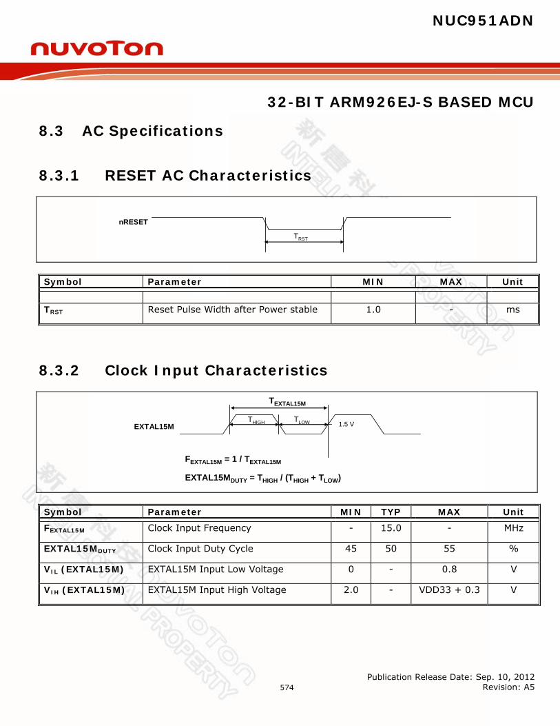
NUC951ADN
32-BIT ARM926EJ-S BASED MCU
Publication Release Date: Sep. 10, 2012 Revision: A5
574
8.3 AC Specifications
8.3.1 RESET AC Characteristics
nRESET
TRST
Symbol Parameter MIN MAX Unit
TRST Reset Pulse Width after Power stable 1.0 - ms
8.3.2 Clock Input Characteristics
EXTAL15M 1.5 VTHIGH TLOW
EXTAL15MDUTY = THIGH / (THIGH + TLOW)
TEXTAL15M
FEXTAL15M = 1 / TEXTAL15M
Symbol Parameter MIN TYP MAX Unit
FEXTAL15M Clock Input Frequency - 15.0 - MHz
EXTAL15MDUTY Clock Input Duty Cycle 45 50 55 %
VIL (EXTAL15M) EXTAL15M Input Low Voltage 0 - 0.8 V
VIH (EXTAL15M) EXTAL15M Input High Voltage 2.0 - VDD33 + 0.3 V

NUC951ADN
32-BIT ARM926EJ-S BASED MCU
Publication Release Date: Sep. 10, 2012 Revision: A5
575
8.3.3 EBI/SDRAM Interface AC Characteristics
MCLK
OutputDelay Output Valid
1.5V
1.5V
TDO
Symbol Parameter MIN MAX Unit
FMCLK SDRAM Clock Output Frequency - 100 MHz TDSU MD[31:0]] Input Setup Time 2 - ns TDH MD[31:0] Input Hold Time 2 - ns TOSU SDRAM Output Signal Valid Delay Time 2* 5* ns
* The above TOSU is based on the EBI CKSKEW register default setting on 0x48 and FMCLK at 100MHz
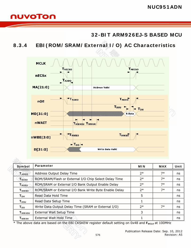
NUC951ADN
32-BIT ARM926EJ-S BASED MCU
Publication Release Date: Sep. 10, 2012 Revision: A5
576
8.3.4 EBI(ROM/SRAM/External I/O) AC Characteristics
Symbol Parameter MIN MAX Unit
TADDO Address Output Delay Time 2* 7* ns
TNCSO ROM/SRAM/Flash or External I/O Chip Select Delay Time 2* 7* ns
TNOEO ROM/SRAM or External I/O Bank Output Enable Delay 2* 7* ns
TNWBO ROM/SRAM or External I/O Bank Write Byte Enable Delay 2* 7* ns
TDH Read Data Hold Time 5 ns
TDSU Read Data Setup Time 1 ns
TDO Write Data Output Delay Time (SRAM or External I/O) 2* 7* ns
TNWASU External Wait Setup Time 3 ns
TNWAH External Wait Hold Time 1 ns * The above data are based on the EBI CKSKEW register default setting on 0x48 and FMCLK at 100MHz
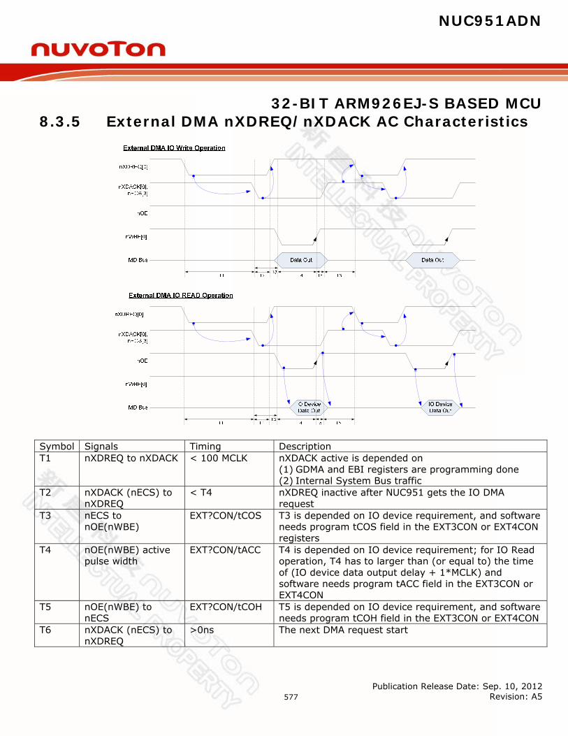
NUC951ADN
32-BIT ARM926EJ-S BASED MCU
Publication Release Date: Sep. 10, 2012 Revision: A5
577
8.3.5 External DMA nXDREQ/nXDACK AC Characteristics
Symbol Signals Timing Description T1 nXDREQ to nXDACK < 100 MCLK nXDACK active is depended on
(1) GDMA and EBI registers are programming done (2) Internal System Bus traffic
T2 nXDACK (nECS) to nXDREQ
< T4 nXDREQ inactive after NUC951 gets the IO DMA request
T3 nECS to nOE(nWBE)
EXT?CON/tCOS T3 is depended on IO device requirement, and software needs program tCOS field in the EXT3CON or EXT4CON registers
T4 nOE(nWBE) active pulse width
EXT?CON/tACC T4 is depended on IO device requirement; for IO Read operation, T4 has to larger than (or equal to) the time of (IO device data output delay + 1*MCLK) and software needs program tACC field in the EXT3CON or EXT4CON
T5 nOE(nWBE) to nECS
EXT?CON/tCOH T5 is depended on IO device requirement, and software needs program tCOH field in the EXT3CON or EXT4CON
T6 nXDACK (nECS) to nXDREQ
>0ns The next DMA request start
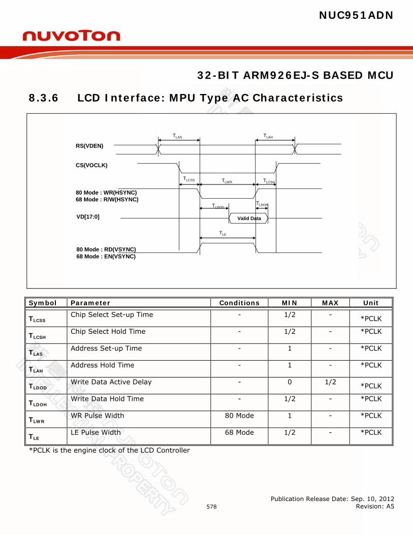
NUC951ADN
32-BIT ARM926EJ-S BASED MCU
Publication Release Date: Sep. 10, 2012 Revision: A5
578
8.3.6 LCD Interface: MPU Type AC Characteristics
CS(VOCLK)
RS(VDEN)
VD[17:0]
80 Mode : WR(HSYNC)68 Mode : R/W(HSYNC)
Valid Data
TLCSHTLCSS
TLDODTLDOH
TLWR
TLAS TLAH
80 Mode : RD(VSYNC)68 Mode : EN(VSYNC)
TLE
Symbol Parameter Conditions MIN MAX Unit
TLCSS Chip Select Set-up Time - 1/2 - *PCLK
TLCSH Chip Select Hold Time - 1/2 - *PCLK
TLAS Address Set-up Time - 1 - *PCLK
TLAH Address Hold Time - 1 - *PCLK
TLDOD Write Data Active Delay - 0 1/2 *PCLK
TLDOH Write Data Hold Time - 1/2 - *PCLK
TLWR WR Pulse Width 80 Mode 1 - *PCLK
TLE LE Pulse Width 68 Mode 1/2 - *PCLK
*PCLK is the engine clock of the LCD Controller

NUC951ADN
32-BIT ARM926EJ-S BASED MCU
Publication Release Date: Sep. 10, 2012 Revision: A5
579
8.3.7 SD Host Interface AC Characteristics
SD_CLK
SD_CMD, SD_DAT[3:0]
TOAD
output valid
SD_CLK
SD_CMD, SD_DAT[3:0]
TISU TIH
input valid
TCLKH
TCLKL
FSD
TOH
Symbol Parameter Conditions MIN MAX Unit
FSD SD Clock Frequency Identification Mode 100 400 KHz
FSD SD Clock Frequency Data Transfer Mode - 50 MHz
TCLKH SD Clock High Time - 10 - ns
TCLKL SD Clock Low Time - 10 - ns
TISU SD CMD & Data Input Setup Time - 5 - ns
TIH SD CMD & Data Input Hold Time - 5 - ns
TOAD SD Output Active Delay (Falling Edge) - - 14 ns
TOH SD Output Hold Time - 0 - ns

NUC951ADN
32-BIT ARM926EJ-S BASED MCU
Publication Release Date: Sep. 10, 2012 Revision: A5
580
8.3.8 NAND Flash Memory Interface AC Characteristics
SM_CS0n,SM_CS1n, SM_ALE, SM_CLE
TWDHTWDS
TWHTWP
TWC
SM_WEn
SM_D[7:0]
TCACSTCACH
WAD-0 WAD-1 WAD-2
TRDHTRDS
TRHTRP
SM_REn
SM_D[7:0]
TCACSTCACH
RD-0 RD-1 RD-2
TRC
Symbol Parameter MIN MAX Unit
TCACS SM_CS0n, SM_CS1n, SM_ALE, SM_CLE Setup Time before SM_WEn, SM_REn Low
20 - ns
TCACH SM_CS0n, SM_CS1n, SM_ALE, SM_CLE Hold Time after SM_WEn, SM_REn High
40 - ns
TWP Write Pulse Width 40 - ns
TWH SM_WEn High Time 20 - ns
TWC Write Cycle Time 80 - ns
TWDS Write Data Output Setup Time 30 - ns
TWDH Write Data Output Hold Time 20 - ns
TRP Read Pulse Width 60 - ns
TRH SM_REn High Time 20 - ns
TRC Read Cycle Time 80 - ns
TRDS Read Data Input Setup Time 6 - ns
TRDH Read Data Input Hold Time 20 - ns
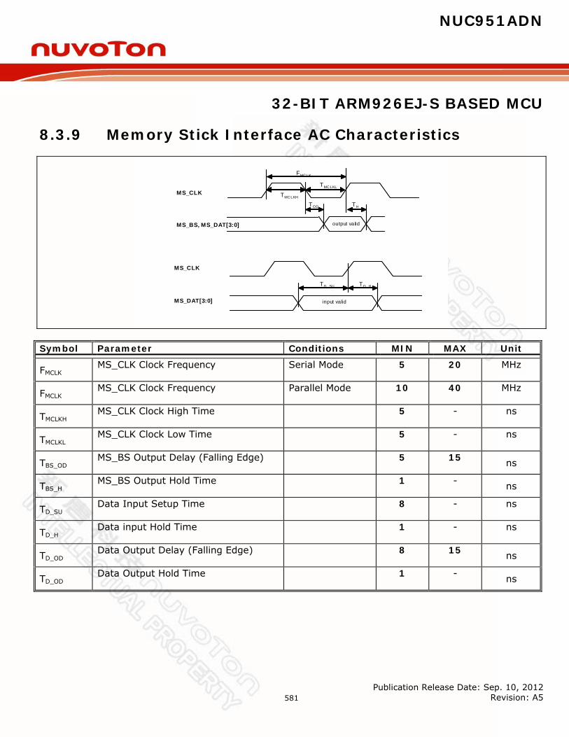
NUC951ADN
32-BIT ARM926EJ-S BASED MCU
Publication Release Date: Sep. 10, 2012 Revision: A5
581
8.3.9 Memory Stick Interface AC Characteristics
MS_CLK
MS_BS, MS_DAT[3:0]
TOD
output valid
MS_CLK
MS_DAT[3:0]
TD_SU TD_H
input valid
TMCLKH
TMC LKL
FMC LK
TH
Symbol Parameter Conditions MIN MAX Unit
FMCLK MS_CLK Clock Frequency Serial Mode 5 20 MHz
FMCLK MS_CLK Clock Frequency Parallel Mode 10 40 MHz
TMCLKH MS_CLK Clock High Time 5 - ns
TMCLKL MS_CLK Clock Low Time 5 - ns
TBS_OD MS_BS Output Delay (Falling Edge) 5 15 ns
TBS_H MS_BS Output Hold Time 1 - ns
TD_SU Data Input Setup Time 8 - ns
TD_H Data input Hold Time 1 - ns
TD_OD Data Output Delay (Falling Edge) 8 15 ns
TD_OD Data Output Hold Time 1 - ns
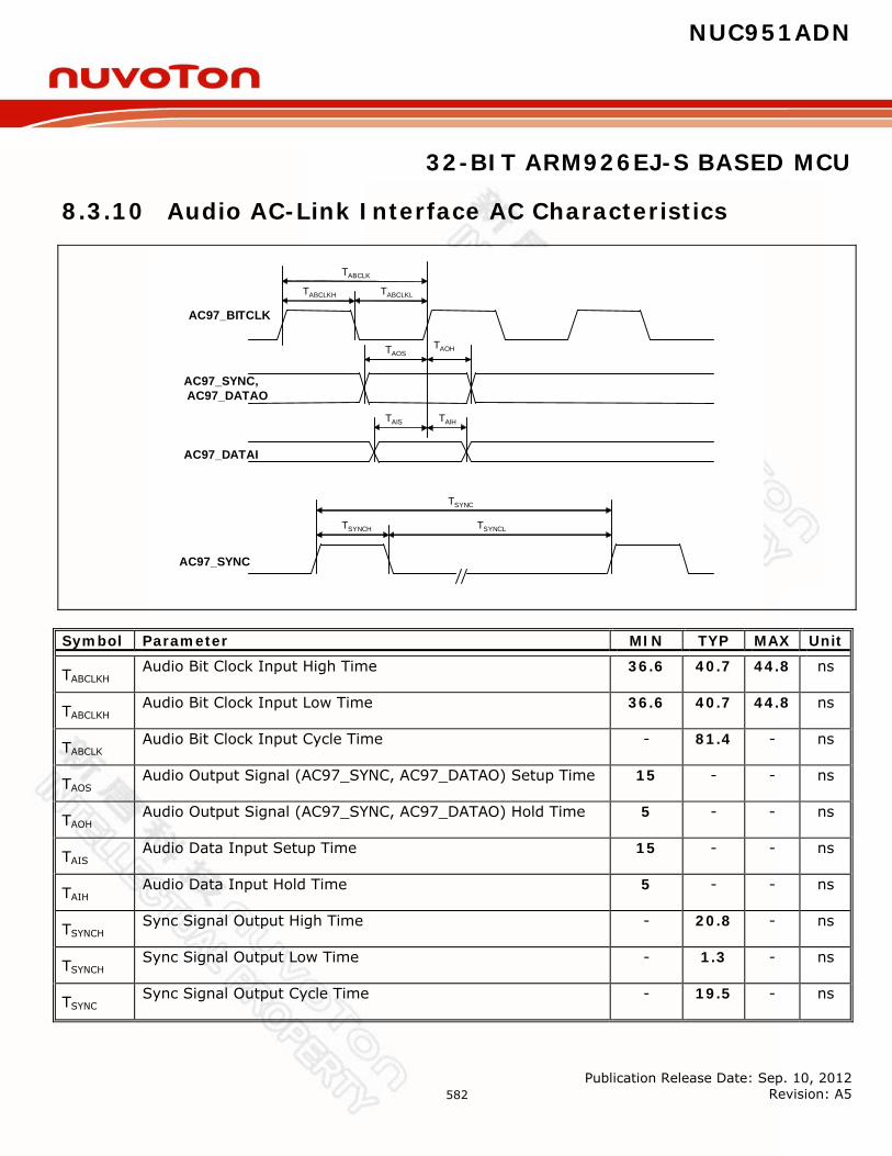
NUC951ADN
32-BIT ARM926EJ-S BASED MCU
Publication Release Date: Sep. 10, 2012 Revision: A5
582
8.3.10 Audio AC-Link Interface AC Characteristics
AC97_BITCLK
AC97_SYNC,AC97_DATAO
TAOSTAOH
AC97_DATAI
TAIS TAIH
TABCLKL
TABCLK
TABCLKH
AC97_SYNC
TSYNC
TSYNCH TSYNCL
Symbol Parameter MIN TYP MAX Unit
TABCLKH Audio Bit Clock Input High Time 36.6 40.7 44.8 ns
TABCLKH Audio Bit Clock Input Low Time 36.6 40.7 44.8 ns
TABCLK Audio Bit Clock Input Cycle Time - 81.4 - ns
TAOS Audio Output Signal (AC97_SYNC, AC97_DATAO) Setup Time 15 - - ns
TAOH Audio Output Signal (AC97_SYNC, AC97_DATAO) Hold Time 5 - - ns
TAIS Audio Data Input Setup Time 15 - - ns
TAIH Audio Data Input Hold Time 5 - - ns
TSYNCH Sync Signal Output High Time - 20.8 - ns
TSYNCH Sync Signal Output Low Time - 1.3 - ns
TSYNC Sync Signal Output Cycle Time - 19.5 - ns

NUC951ADN
32-BIT ARM926EJ-S BASED MCU
Publication Release Date: Sep. 10, 2012 Revision: A5
583
8.3.11 Audio I2S Interface AC Characteristics
I2S_BITCLK
I2S_WS, I2S_DATAO
TAOS TAOH
I2S_BITCLK
I2S_DATAI
TAIS TAIH
TABCLKL
TABCLK
TABCLKH
Symbol Parameter MIN MAX Unit
TABCLKH Audio Bit Clock Output High Time 18.3 - ns
TABCLKH Audio Bit Clock Output Low Time 18.3 - ns
TABCLK Audio Bit Clock Output Cycle Time 40.7 - ns
TAOS Audio Data Output Setup Time 4.5 - ns
TAOH Audio Data Output Hold Time 4.5 - ns
TAIS Audio Data Input Setup Time 4.5 - ns
TAIH Audio Data Input Hold Time 4.5 - ns
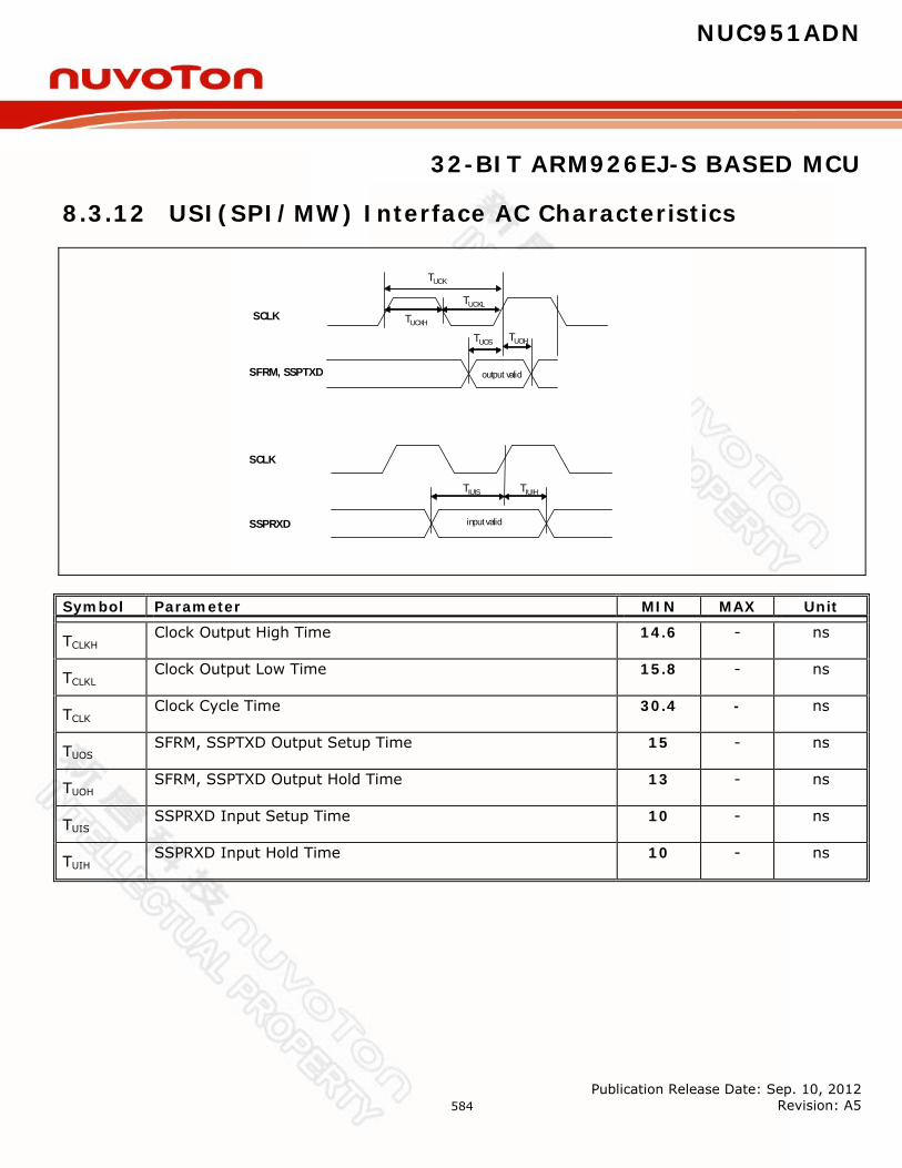
NUC951ADN
32-BIT ARM926EJ-S BASED MCU
Publication Release Date: Sep. 10, 2012 Revision: A5
584
8.3.12 USI(SPI/MW) Interface AC Characteristics
SCLK
SFRM, SSPTXD
TUOS
output valid
SCLK
SSPRXD
TIUIS TIUIH
input valid
TUCKH
TUCKL
TUCK
TUOH
Symbol Parameter MIN MAX Unit
TCLKH Clock Output High Time 14.6 - ns
TCLKL Clock Output Low Time 15.8 - ns
TCLK Clock Cycle Time 30.4 - ns
TUOS SFRM, SSPTXD Output Setup Time 15 - ns
TUOH SFRM, SSPTXD Output Hold Time 13 - ns
TUIS SSPRXD Input Setup Time 10 - ns
TUIH SSPRXD Input Hold Time 10 - ns
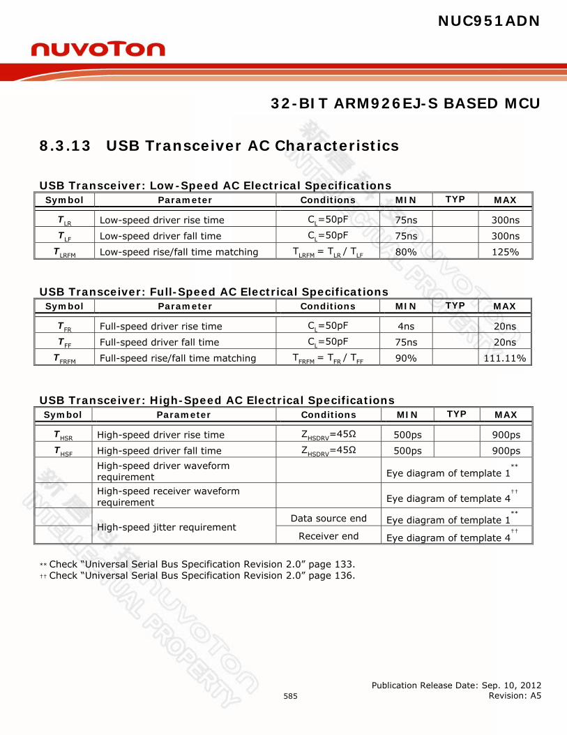
NUC951ADN
32-BIT ARM926EJ-S BASED MCU
Publication Release Date: Sep. 10, 2012 Revision: A5
585
8.3.13 USB Transceiver AC Characteristics
USB Transceiver: Low-Speed AC Electrical Specifications Symbol Parameter Conditions MIN TYP MAX
TLR Low-speed driver rise time CL=50pF 75ns 300ns TLF Low-speed driver fall time CL=50pF 75ns 300ns
TLRFM Low-speed rise/fall time matching TLRFM = TLR / TLF 80% 125% USB Transceiver: Full-Speed AC Electrical Specifications Symbol Parameter Conditions MIN TYP MAX
TFR Full-speed driver rise time CL=50pF 4ns 20ns TFF Full-speed driver fall time CL=50pF 75ns 20ns
TFRFM Full-speed rise/fall time matching TFRFM = TFR / TFF 90% 111.11% USB Transceiver: High-Speed AC Electrical Specifications Symbol Parameter Conditions MIN TYP MAX
THSR High-speed driver rise time ZHSDRV=45Ω 500ps 900ps THSF High-speed driver fall time ZHSDRV=45Ω 500ps 900ps
High-speed driver waveform requirement Eye diagram of template 1
**
High-speed receiver waveform requirement Eye diagram of template 4
††
High-speed jitter requirement
Data source end Eye diagram of template 1**
Receiver end Eye diagram of template 4††
** Check “Universal Serial Bus Specification Revision 2.0” page 133. †† Check “Universal Serial Bus Specification Revision 2.0” page 136.
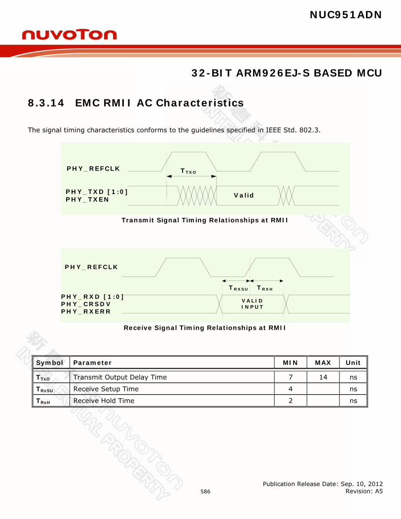
NUC951ADN
32-BIT ARM926EJ-S BASED MCU
Publication Release Date: Sep. 10, 2012 Revision: A5
586
8.3.14 EMC RMII AC Characteristics The signal timing characteristics conforms to the guidelines specified in IEEE Std. 802.3.
PHY_REFCLK
PHY_TXD [1:0]PHY_TXEN
TTXO
Valid
Transmit Signal Timing Relationships at RMII
PHY_REFCLK
PHY_RXD [1:0]PHY_CRSDVPHY_RXERR
VALID IN PUT
TRXHTRXSU
Receive Signal Timing Relationships at RMII
Symbol Parameter MIN MAX Unit
TTxO Transmit Output Delay Time 7 14 ns
TRxSU Receive Setup Time 4 ns
TRxH Receive Hold Time 2 ns

NUC951ADN
32-BIT ARM926EJ-S BASED MCU
Publication Release Date: Sep. 10, 2012 Revision: A5
587
P H Y _ M D C
P H Y _ M D IOV A L ID IN P U T
T M D HT M D S U
PHY_MDIO Read from PHY Timing
PHY_MDC
PHY_MDIO
TMDO
Valid
PHY_MDIO Write to PHY Timing
Symbol Parameter MIN MAX Unit
TMDO PHY_MDIO Output Delay Time 0 15 ns
TMDSU PHY_MDIO Setup Time 5 ns
TMDH PHY_MDIO Hold Time 5 ns
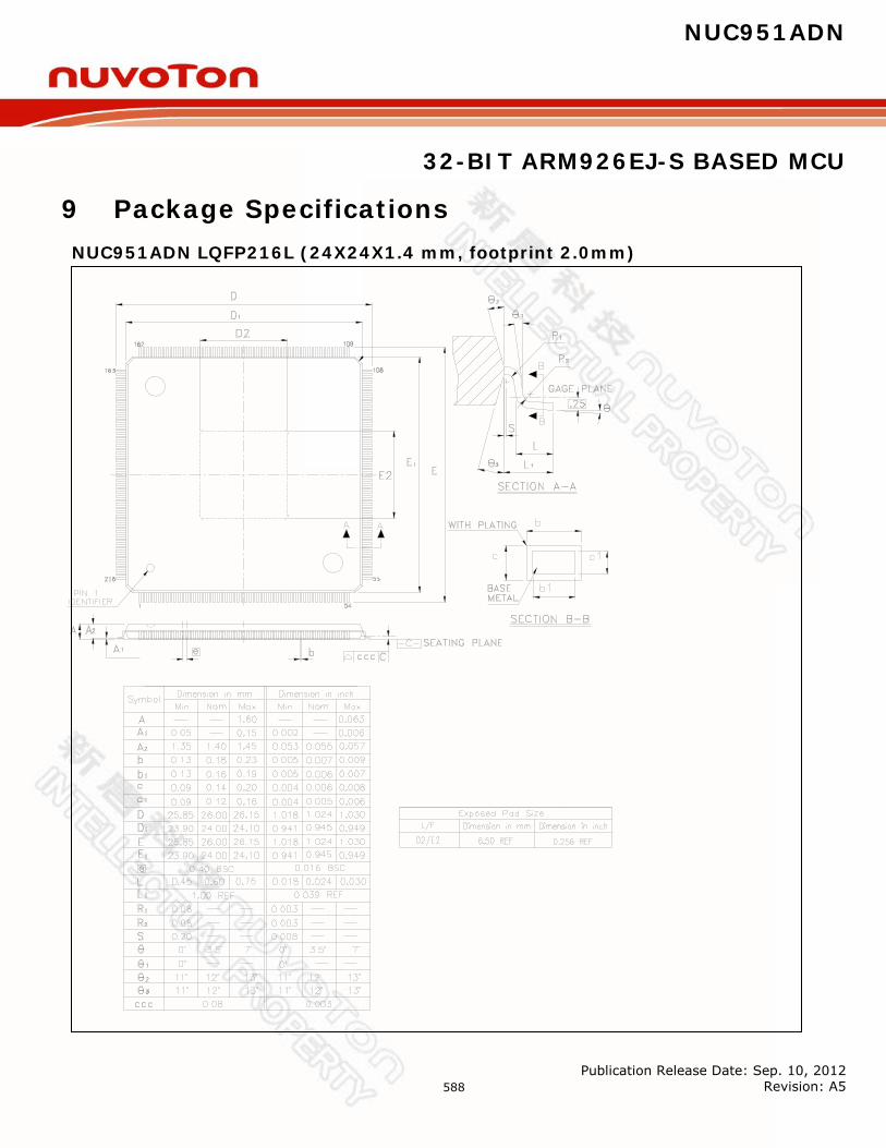
NUC951ADN
32-BIT ARM926EJ-S BASED MCU
Publication Release Date: Sep. 10, 2012 Revision: A5
588
9 Package Specifications NUC951ADN LQFP216L (24X24X1.4 mm, footprint 2.0mm)
NUC951ADN
32-BIT ARM926EJ-S BASED MCU
Publication Release Date: Sep. 10, 2012 Revision: A5
589
10 Revision History Revision Date Comments
A 2008/07/09 First Release
A1 2008/07/18 Update Chapter 7.11
Display size: Maximum size 1024x768
A2 2008/10/07
1. Change Part Number from W90P910CBG to W90P910CBN
2. Update Chapter 2
Add text “Pb free, Halogen free”
3. Correct Typo: Spelling and grammar check
A3 2009/04/13
1. Update Chapter 7.11.1.4
Display Pin Assignment Table
2. Rename nWE to nSWE 3. Update Chapter 7.11
Display size: Maximum size 1024x600
4. Change Part Number from W90P910CBN to NUC910ABN
5. Update Chapter 8.3.5
LCD Interface: MPU Type AC Characteristics
A4 2010/06/18 1. Add IOH, IOL current value
A5 2012/09/10
1. Update Chapter 4 Pin Assignment 2. Update Chapter 5 Pin Description 3. Update Chapter 8.3.4 EBI timing diagram. 4. Update Chapter 9 Package Specification 5. Update descriptions of register MFSEL bit
[13:8].
NUC951ADN
32-BIT ARM926EJ-S BASED MCU
Publication Release Date: Sep. 10, 2012 Revision: A5
590
Important Notice
Nuvoton Products are neither intended nor warranted for usage in systems or equipment, any malfunction or failure of which may cause loss of human life, bodily injury or severe property damage. Such applications are deemed, “Insecure Usage”.
Insecure usage includes, but is not limited to: equipment for surgical implementation, atomic energy control instruments, airplane or spaceship instruments, the control or operation of dynamic, brake or safety systems designed for vehicular use, traffic signal instruments, all types of safety devices, and other applications intended to support or sustain life.
All Insecure Usage shall be made at customer’s risk, and in the event that third parties lay claims to Nuvoton as a result of customer’s Insecure Usage, customer shall indemnify the damages and liabilities thus incurred by Nuvoton.