NOVEL MATERIALS GROUP - hu-berlin.de
3
Could you introduce your Novel Materials research group, outlining its overarching interests? My team and I investigate novel electronic materials in three areas: functional nanomaterials (eg. for thermoelectrics); quantum materials for future quantum and spin electronics; and artificial ultra-thin layers for fundamental investigations of emergent phenomena like superconductivity and charge- density waves. What drives your interest in this area? As a physicist, curiosity drives me to understand solid materials under special conditions. For example, in our everyday use of IT we have a high demand to process huge amounts of data quickly and thus electronic circuits have shrunk drastically in size. Often materials used in these circuits are really only a few tens of nanometres in scale or less. However, in the nanoworld we find that carriers of electrical charge, electrons or holes do not only behave as particles but also have a wave nature. Here, quantum physics plays its wonderful tricks, and changing electrical and magnetic fields or temperature in experiments can give a lot of insight – and is fun! How fundamental is a collaborative, multidisciplinary approach to your research? It is a full prerequisite. We require collaboration with experts who fabricate novel materials, who investigate crystal structure and composition, or who are able to produce experimental tools. In turn, we offer the full investigation of charge, spin and thermal transport, as well as insight into the underlying physics phenomena. With the German Federal Ministry of Education and Research (BMBF) highlighting energy harvesting as one of eight important technology areas, how does your research group approach the issue and provide environmental energy solutions? Energy harvesting is about transforming energy from the environment to power electrical devices, ideally without the use of another electrical power supply. At present there is a worldwide search to increase the efficiency of thermoelectric materials. We are proud to be part of two collaborative projects together with researchers from Hamburg, Freiburg, Würzburg and Bilbao within the German priority programme on nanostructured thermoelectrics (SPP1386), funded by the German Research Foundation (DFG). Thermoelectric materials enable us to provide electrical energy from a temperature difference in the environment, as from the heat of a car engine or from a computer processor that is processing our data ‘hard’. However, thermoelectric materials applicable for mass production have a rather low efficiency because the physical mechanisms that allow heat flow through a material are coupled to those permitting charge flow. We therefore investigate novel nanomaterials for which the aim is to understand and decouple these physical mechanisms. What are the great challenges in this field? In order to design novel thermoelectric materials, we need a fundamental understanding of the underlying physics. Therefore, thermoelectrical properties and crystal and surface structure, defects and chemical homogeneity have to be measured accurately and identically for every nanoscale material sample. This is quite tricky – challenging both technologically and experimentally! In terms of more general novel materials research, everyday challenges involve finding the key parameters in a real-life experiment and environment. In each investigation, the experimental setup and unknown novel material offer numerous parameters that can be changed. My students, co-workers and I have to make correct, educated guesses in order to advance. Our strategy is quite old- fashioned: check the basics! Only then do we advance, take a risk and, if possible, keep it simple. Could you describe some of your successes within this area to date? Within SPP1386, we were able to demonstrate the feasibility of full thermoelectrical characterisation of single nanowires in combination with full structural and chemical analysis. This required the best electronic measurement setups allowing temperature-dependent low-noise electrical analyses, investigations with a high-resolution transmission electron microscope supplied with chemical analysis tools, and excellent collaboration with partners who provided nanowires and worked with us on fabricating a suitable nanowire measurement platform. As a result, our expertise has been recognised by colleagues in Korea conducting similar work on increasing the efficiency of nanostructured thermoelectric materials and we are looking forward to an extended research exchange, eg. working towards a worldwide standard in thermoelectrical measurements for nanomaterials. International Innovation speaks with Professor Saskia F Fischer about the groundbreaking work her research group is conducting in the field of novel electronic materials, particularly in relation to nanostructured thermoelectrics Novel nanostructures www.internationalinnovation.com 35 PROFESSOR SASKIA FLORINE FISCHER
Transcript of NOVEL MATERIALS GROUP - hu-berlin.de

Could you introduce your Novel Materials research group, outlining its overarching interests?
My team and I investigate novel electronic materials in three areas: functional nanomaterials (eg. for thermoelectrics); quantum materials for future quantum and spin electronics; and artificial ultra-thin layers for fundamental investigations of emergent phenomena like superconductivity and charge-density waves.
What drives your interest in this area?
As a physicist, curiosity drives me to understand solid materials under special conditions. For example, in our everyday use of IT we have a high demand to process huge amounts of data quickly and thus electronic circuits have shrunk drastically in size. Often materials used in these circuits are really only a few tens of nanometres in scale or less. However, in the nanoworld we find that carriers of electrical charge, electrons or holes do not only behave as particles but also have a wave nature. Here, quantum physics plays its wonderful tricks, and changing electrical and magnetic fields or temperature in experiments can give a lot of insight – and is fun!
How fundamental is a collaborative, multidisciplinary approach to your research?
It is a full prerequisite. We require collaboration with experts who fabricate novel materials, who investigate crystal structure and composition, or who are able to produce experimental tools. In turn, we offer the full investigation of charge, spin and thermal transport, as well as insight into the underlying physics phenomena.
With the German Federal Ministry of Education and Research (BMBF) highlighting energy harvesting as one of eight important technology areas, how does your research group approach the issue and provide environmental energy solutions?
Energy harvesting is about transforming energy from the environment to power electrical devices, ideally without the use of another electrical power supply. At present there is a worldwide search to increase the efficiency of thermoelectric materials. We are proud to be part of two collaborative projects together with researchers from Hamburg, Freiburg, Würzburg and Bilbao within the German priority programme on nanostructured thermoelectrics (SPP1386), funded by the German Research Foundation (DFG).
Thermoelectric materials enable us to provide electrical energy from a temperature difference in the environment, as from the heat of a car engine or from a computer processor that is processing our data ‘hard’. However, thermoelectric materials applicable for mass production have a rather low efficiency because the physical mechanisms that allow heat flow through a material are coupled to those permitting charge flow. We therefore investigate novel nanomaterials for which the aim is to understand and decouple these physical mechanisms.
What are the great challenges in this field?
In order to design novel thermoelectric materials, we need a fundamental understanding of the underlying physics. Therefore, thermoelectrical properties and crystal and surface structure, defects and chemical homogeneity have to be measured accurately and identically for every
nanoscale material sample. This is quite tricky – challenging both technologically and experimentally!
In terms of more general novel materials research, everyday challenges involve finding the key parameters in a real-life experiment and environment. In each investigation, the experimental setup and unknown novel material offer numerous parameters that can be changed. My students, co-workers and I have to make correct, educated guesses in order to advance. Our strategy is quite old-fashioned: check the basics! Only then do we advance, take a risk and, if possible, keep it simple.
Could you describe some of your successes within this area to date?
Within SPP1386, we were able to demonstrate the feasibility of full thermoelectrical characterisation of single nanowires in combination with full structural and chemical analysis. This required the best electronic measurement setups allowing temperature-dependent low-noise electrical analyses, investigations with a high-resolution transmission electron microscope supplied with chemical analysis tools, and excellent collaboration with partners who provided nanowires and worked with us on fabricating a suitable nanowire measurement platform.
As a result, our expertise has been recognised by colleagues in Korea conducting similar work on increasing the efficiency of nanostructured thermoelectric materials and we are looking forward to an extended research exchange, eg. working towards a worldwide standard in thermoelectrical measurements for nanomaterials.
International Innovation speaks with Professor Saskia F Fischer about the groundbreaking work her research group is conducting in the field of novel electronic materials, particularly in relation to nanostructured thermoelectrics
Novel nanostructures
www.internationalinnovation.com 35
PROFESSOR SASKIA FLORINE FISCHER
AT THE HUMBOLDT-UNIVERSITÄT ZU BERLIN, Germany, Professor Saskia F Fischer leads the Novel Materials research group in its efforts to help shape the materials required for future electronic applications. By investigating transport phenomena in quantum, nano- and thin-film materials, the researchers aim to shine a light on the fundamental physics of nanostructures and their hybrid systems.
To facilitate these studies, the team uses experimental techniques that allow electrical conductivity, magnetoresistance and electrical noise to be determined. A full thermoelectric characterisation is achieved by measuring the electrical and thermal conductivity and the Seebeck coefficient against a range of temperatures and electromagnetic fields. In order to successfully interpret results, precise knowledge of crystal structure, microstructure, possible atomic defects and boundary nature is required. The Novel Materials group therefore conducts structure and topography investigations with the aid of high-resolution transmission electron, atomic force and optical microscopy. Finally, to fabricate nanostructures within the lab, the team utilises ‘top-down’ lithography, ‘bottom-up’ growth methods and a variety of etching techniques.
ENERGY HARVESTING AND THERMOELECTRICSEnergy harvesting – scavenging energy from the environment to power electrical devices without the need for an external power supply – has been identified by the German Ministry of Education and Research (BMBF) as one of this decade’s most pressing science and technology priority areas. It is hoped that, ultimately,
energy harvesting could have applications within the meteorological, geophysical and engineering sectors, where it could be used to power monitoring instruments, as well as for medical, consumer and transport devices. However, if such feats are to be accomplished, the principle transformations involved – the conversion of solar, vibration or heat energy into electrical energy – must be further investigated and developed on a fundamental level.
Thermoelectric materials provide a particularly interesting opportunity in relation to energy harvesting. These materials are capable of converting environmental heat into electrical energy, and hold promise in terms of recovering heat waste such as that which radiates from a car engine, computer processor or house – although they could be employed in any environment in which there is a temperature difference. However, current thermoelectric materials have so far only achieved relatively low conversion efficiencies, which has hindered their widespread application.
NOVEL NANOSTRUCTURESIt is for this reason that the German Research Foundation (DFG) is funding Fischer and her Novel Materials group’s research on this topic, alongside a diverse collection of collaborators, to search for ways in which this efficiency can be improved, as part of a materials research priority programme on nanostructured thermoelectrics (SPP1386). “Thermoelectric nanostructures enable the improvement of thermoelectric efficiency through the formation of barriers within materials that hinder heat flow and thus keep temperature gradient high while allowing easy electrical charge
carrier transmission,” Fischer outlines. At present, the team is particularly interested in investigating porous or nanocrystalline silicon compounds, as these are low-cost, widely and sustainably available, present no health risks and are easy to process.
Within the DFG priority programme, Fischer is co-initiator and project partner of two projects investigating the thermoelectric properties of nanowires and quantum wires. The Novel Materials group has already seen significant success, achieving full thermoelectrical characterisation of single nanowires, with combined insight into their chemistry, crystal structure and topography at the nanoscale. “Our studies demonstrate that it is possible to acquire all experimental parameters of one individual nanoscale object, such as a nanowire,” Fischer elaborates. “For example, we can unambiguously show changes in a material’s thermoelectrical
Thermoelectric nanowire platform (upper left) showing crystal diffraction pattern (upper right) and the nanowire (bottom).
Danny Kojda and Dr Rüdiger Mitdank.
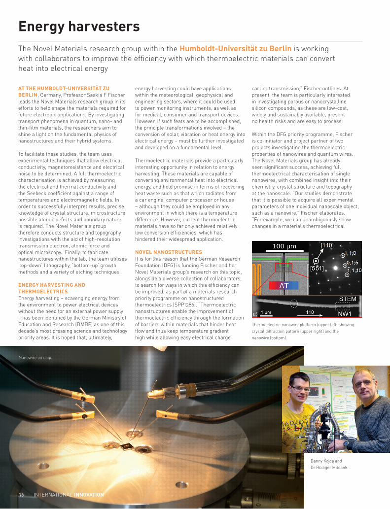
Nanowire on chip.
The Novel Materials research group within the Humboldt-Universität zu Berlin is working with collaborators to improve the efficiency with which thermoelectric materials can convert heat into electrical energy
Energy harvesters
36 INTERNATIONAL INNOVATION
NOVEL MATERIALS GROUP
OBJECTIVESTo investigate novel electronic materials in three areas:
• Functional nanomaterials – such as for thermoelectrics
• Quantum materials for future quantum and spin electronics
• Artificial ultra-thin layers for fundamental investigations of emergent phenomena
KEY COLLABORATORSProfessor Kornelius Nielsch; Professor Wolfgang Hansen, Universität Hamburg, Germany • Professor Peter Woias, Institut für Mikrosystemtechnik – IMTEK Universität Freiburg, Germany • Professor Hartmut Buhmann; Universität Würzburg, Germany • Professor Jens Siewert, University of the Basque Country, Bilbao, Spain • Professor Bruce McCombe, State University of New York at Buffalo, USA • Professor David Johnson, University of Oregon, USA • Professor Oliver Rader, Helmholtz-Zentrum Berlin für Materialien und Energie, Germany • Professur Hubert Ebert, Ludwig-Maximilians-Universität München, Germany
FUNDINGGerman Research Foundation (DFG)
Materials World Network Program
CONTACTProfessor Dr Saskia Florine Fischer Chair, Novel Materials group
Faculty of Mathematics and Natural Sciences Department of Physics Humboldt-Universität zu Berlin Newtonstrasse 15 12489 Berlin Germany
T +49 302 093 8044 E [email protected]
www.physik.hu-berlin.de/gnm
www.researchgate.net/profile/Saskia_Fischer2
http://linkd.in/1DzVOvl
PROFESSOR SASKIA F FISCHER has led the Novel Materials group as Professor for Experimental Physics at Humboldt-Universität zu Berlin, Germany, since
2010. Fischer’s research contributes to fields of novel electronic materials for future nano- and spinelectronics and energy harvesting applications. Her special interest is in correlating physical and structural properties. As well as leading various international joint research collaborations, Fischer is the co-initiator of two DFG-funded priority programmes; ‘Nanostructured thermoelectrics’ and ‘Topological insulators’.
INTELLIGENCE
properties due to size effects, or identify the ratio between thermal and electrical conductivity (Lorenz number) in its particular temperature dependence.” As a result of this breakthrough, the team is now starting a collaboration with a group in Korea. Generally, a key interest is to establish an international standard in the thermoelectrical measurement of nanomaterials.
Of course, this progress could not have been achieved without encountering considerable challenges along the way. “Many researchers before us had tried to do the most sensible thing: take a shortcut, investigate only what was easily accessible in their labs and take the missing data from other studies. However, these shortcuts always produced controversies,” Fischer explains. “We decided to do the ‘full homework’ and redesign all experiments using an all-in-one device. The whole process was terribly tedious, a lot of work and required the best of three collaborating research groups.”
SPREADING THEIR NETThe Novel Materials group’s work is not limited to thermoelectric materials alone, but also covers a range of other research topics. Firstly, the team investigates quantum systems with respect to the way in which electrical fields, low and high magnetic fields, temperature and non-thermal equilibrium affect charge, spin and thermal transport properties in one-, two- and zero-dimensional structures. Quantum coherence and decoherence are of particular interest to the researchers in this regard.
Secondly, the team is investigating electronic nanostructures of all natures, not just thermoelectric. Size effects of the electrical conductivity, magnetoresistance and voltage or current noise across varying electrical fields, low and high magnetic fields, temperatures and temperature gradients are studied, and measuring techniques optimised.
Thirdly, the group conducts research on ultra-thin layers, exploring the extent to which transport performance of topological insulators, semiconductor/superconductor
hybrids and metal/semiconductor oxide hybrids is affected by electrical fields, low and high magnetic fields and temperature. With respect to this area, topological surface states, phase transitions to emergent phenomena and proximity effects at hybrid interfaces are major areas of study for the scientists.
NOVEL MATERIALS, NEW BEGINNINGSAt present, the Novel Materials group is involved in a number of exciting collaborations that are likely to produce fruitful findings in the near future. By working with colleagues from across Germany, Spain, the US, Korea and even further afield, it seems probable that the team’s contributions to fundamental understanding of the physics phenomena relevant to novel materials design will have significant applications in the years to come, and on a worldwide scale.
DATES FOR YOUR DIARY
The Novel Materials group will be presenting its findings at the following events:
German Physics Society Spring Meeting 15-20 March – Berlin, Germany
Conference on Energy Harvesting & Storage Europe 28-29 April – Berlin, Germany
Joint International Conference on Thermoelectrics (ICT) & European Conference on Thermoelectrics (ECT) 28 June-2 July – Dresden, Germany
Joint International Conference: 21st International Conference on Electronic Properties of Two-Dimensional Systems (EP2DS) & 17th International Conference on Modulated Semiconductor Structures (MSS-17) 26-31 July – Tokyo, Japan
Quantum transport crew.
www.internationalinnovation.com 37