
Novel, Four-Switch, Z-Source Three-Phase Inverter BRIEF DESC · 2.) Novel, Four-Switch, Z-Source...
14
2.) Novel, Four-Switch, Z-Source Three-Phase Inverter The scope of this project: Design, build and test a NEW low switch count Z-source (Z-source=voltage boost capability in the dc-link without any extra switches, using only the switches from the inverter bridge and a passive LC network in the dc-link for output voltage modulation and also for voltage boost in the dc-link) three-phase inverter. (Part of my PhD thesis) My main activities and responsibilities in the project - analytically derive the equations describing the operation of the newly proposed topology based on space vector analysis - simulate the inverter using PSIM & Matlab/Simulink and write the control algorithm in C++ language in Visual C++ - design the PCBs for the main and for the control circuits in Orcad Layout - manufacture the PCBs - implement the control algorithm in MPlab from Microchip in C language, program the digital signal processor dsPIC30F4011 - make measurements on the lab setup - and finally write an article containing the theory, simulation and experimental results for a conference Brief description of the project The idea of this new topology started from an existing Z-source DC-AC converter topology shown in Fig. 1 Fig. 1. Three-phase Z-source inverter with six switches The only difference between a traditional three-phase inverter with six switches and the topology shown above is the passive Z-impedance network (one front-end diode D 1 , two inductors L 1 & L 2 and two X connected capacitors C 1 and C 2 ). In essence these Z-source inverters are self-boosting unidirectional dc-ac converters with only six power switches, which are used with some PWM strategies to short-circuit the z- source network by gating at least two transistors on the same inverter-leg AT THE SAME TIME! (e.g. T 1 &T 2 ) and thus produce dc-link voltage boosting on capacitors C 1 and C 2 , V in becomes greater than the input voltage V DC . Of course these short-circuits in
Transcript of Novel, Four-Switch, Z-Source Three-Phase Inverter BRIEF DESC · 2.) Novel, Four-Switch, Z-Source...

2.) Novel, Four-Switch, Z-Source Three-Phase Inverter
The scope of this project: Design, build and test a NEW low switch count Z-source (Z-source=voltage boost capability in the dc-link without any extra switches, using only the switches from the inverter bridge and a passive LC network in the dc-link for output voltage modulation and also for voltage boost in the dc-link) three-phase inverter. (Part of my PhD thesis)
My main activities and responsibilities in the project - analytically derive the equations describing the operation of the newly proposed
topology based on space vector analysis - simulate the inverter using PSIM & Matlab/Simulink and write the control
algorithm in C++ language in Visual C++ - design the PCBs for the main and for the control circuits in Orcad Layout - manufacture the PCBs - implement the control algorithm in MPlab from Microchip in C language,
program the digital signal processor dsPIC30F4011 - make measurements on the lab setup - and finally write an article containing the theory, simulation and experimental
results for a conference Brief description of the project
The idea of this new topology started from an existing Z-source DC-AC converter topology shown in Fig. 1
Fig. 1. Three-phase Z-source inverter with six switches
The only difference between a traditional three-phase inverter with six switches
and the topology shown above is the passive Z-impedance network (one front-end diode D1, two inductors L1 & L2 and two X connected capacitors C1 and C2). In essence these Z-source inverters are self-boosting unidirectional dc-ac converters with only six power switches, which are used with some PWM strategies to short-circuit the z-source network by gating at least two transistors on the same inverter-leg AT THE SAME TIME! (e.g. T1&T2) and thus produce dc-link voltage boosting on capacitors C1 and C2, Vin becomes greater than the input voltage VDC. Of course these short-circuits in
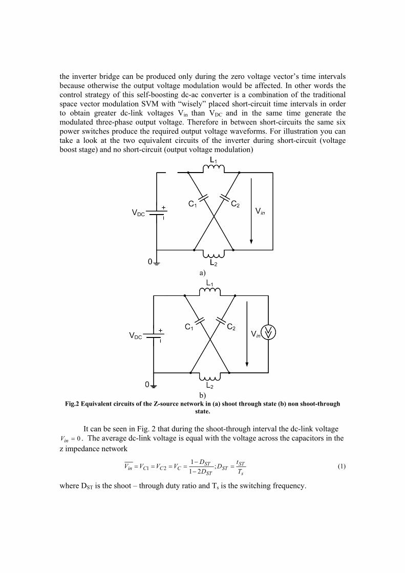
the inverter bridge can be produced only during the zero voltage vector’s time intervals because otherwise the output voltage modulation would be affected. In other words the control strategy of this self-boosting dc-ac converter is a combination of the traditional space vector modulation SVM with “wisely” placed short-circuit time intervals in order to obtain greater dc-link voltages Vin than VDC and in the same time generate the modulated three-phase output voltage. Therefore in between short-circuits the same six power switches produce the required output voltage waveforms. For illustration you can take a look at the two equivalent circuits of the inverter during short-circuit (voltage boost stage) and no short-circuit (output voltage modulation)
a)
b)
Fig.2 Equivalent circuits of the Z-source network in (a) shoot through state (b) non shoot-through state.
It can be seen in Fig. 2 that during the shoot-through interval the dc-link voltage
0=inV . The average dc-link voltage is equal with the voltage across the capacitors in the z impedance network
s
STST
ST
STCCCin T
tDD
DVVVV =−−
==== ;21
121 (1)
where DST is the shoot – through duty ratio and Ts is the switching frequency.

Fig. 3 Relationship between capacitor voltages Cv /dc input voltage DCV and shoot-through time
duty ratio STD Fig. 3 and eq. 1 clearly show that at a 0.5 shoot-through duty ratio the voltage
across the capacitors is infinite, theoretically. In practice measures should be taken to avoid excessive increase of the shoot-through time.
The proposed topology combines the advantages of a traditional four-switch three-phase inverter with the advantages of the z impedance network. This new topology, besides the self-boost property, has low switch count and it can operate as a buck-boost inverter. In contrast to standard four-switch three-phase inverter which operates at half dc input voltage the proposed four-switch z-source inverter, by self- boosting, brings the output voltage at the same (or higher) value as in six switch standard three-phase inverter. The proposed topology:
Fig. 4 Four-switch z-source three-phase inverter.
The analytically derived possible space vectors for the newly proposed topology
can be expressed as

( ) ( )
( ) ( )
DCST
DC
DC
DC
DC
kVV
VkjkV
kVV
VkjkV
VkV
31
12331
3131
12331
31
32
4
3
2
1
−=
⎥⎥⎦
⎤
⎢⎢⎣
⎡+−+−=
−=
⎥⎥⎦
⎤
⎢⎢⎣
⎡−+−=
⎟⎠⎞
⎜⎝⎛ −=
(2)
We can notice that the dc-link voltage boost mode (both switches on at least one inverter leg on) introduced a new voltage vector VST.

Fig. 6. Locations of the voltage vectors in the complex plane
In Fig.6 K is the dc-link voltage boost ratio Vin/VDC. And finally the expressions of a desired prescribed output voltage vector
components vα and vβ can be described by
( ) ( )( ) ( )[ ]
( )( )1233
1233
42
3421
−−=
+−−++−=
kttTVv
kttkttktT
Vv
s
DCs
STs
DCs
β
α
(3)
The principle of the gating signal generation for the four switches implemented in the simulation and in the digital signal processor dsPIC30F3011 is shown in Fig. 7.
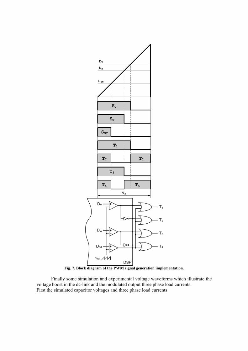
Fig. 7. Block diagram of the PWM signal generation implementation.
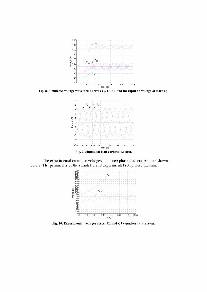
Finally some simulation and experimental voltage waveforms which illustrate the
voltage boost in the dc-link and the modulated output three phase load currents. First the simulated capacitor voltages and three phase load currents
0 0.1 0.2 0.3 0.4 0.520
40
60
80
100
120
140
160
180
200
Time [s]
Vol
tage
[V]
VC1
VC3
VC2
VDC
Fig. 8. Simulated voltage waveforms across C1, C2, C3 and the input dc voltage at start-up.
0.24 0.25 0.26 0.27 0.28 0.29 0.3 0.31-5
-4
-3
-2
-1
0
1
2
3
4
5
Time [s]
Cur
rent
[A]
IVI
UIW
Fig. 9. Simulated load currents (zoom).
The experimental capacitor voltages and three-phase load currents are shown
below. The parameters of the simulated and experimental setup were the same.
0 0.05 0.1 0.15 0.2 0.25 0.3 0.350
102030405060708090
100110120130140150160170180190200
Time [s]
Vol
tage
[V]
VC3
VC1
Fig. 10. Experimental voltages across C1 and C3 capacitors at start-up.
0 0.01 0.02 0.03 0.04 0.05 0.06 0.07-5
-4
-3
-2
-1
0
1
2
3
4
5
Time [s]
Cur
rent
[A]
IW
IVI
U
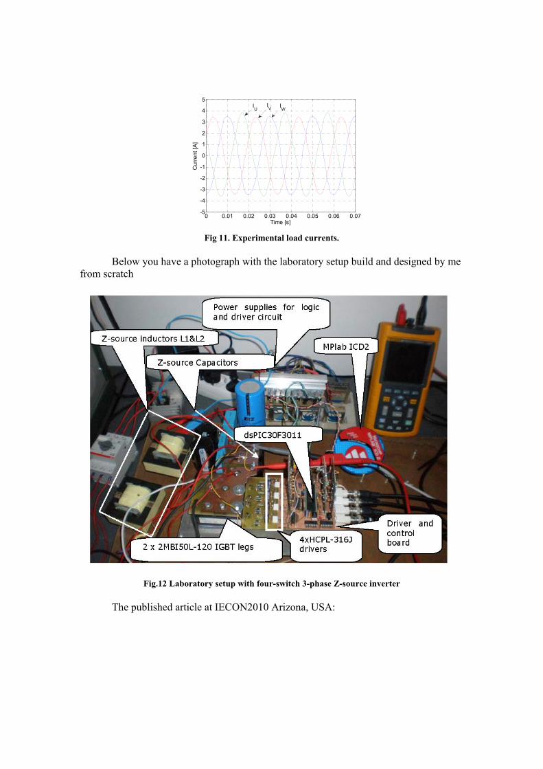
Fig 11. Experimental load currents.
Below you have a photograph with the laboratory setup build and designed by me
from scratch
Fig.12 Laboratory setup with four-switch 3-phase Z-source inverter
The published article at IECON2010 Arizona, USA:

Novel, Four-Switch, Z-Source Three-Phase Inverter
Róbert Antal1, Nicolae Muntean1, Ion Boldea1, Frede Blaabjerg2 1 Politehnica University of Timisoara/Department of Electrical Engineering, Timisoara, Romania
2Institute of Energy Technology, Aalborg University, DK – 9220 Aalborg East, Denmark e-mail:[email protected];
Abstract-This paper presents a new z-source three phase in-
verter topology. The proposed topology combines the advan-tages of a traditional four-switch three-phase inverter with the advantages of the z impedance network (one front-end diode, two inductors and two X connected capacitors). This new topol-ogy, besides the self-boost property, has low switch count and it can operate as a buck-boost inverter. In contrast to standard four-switch three-phase inverter which operates at half dc input voltage the proposed four-switch z-source inverter, by self boost-ing, brings the output voltage at same (or higher) value as in six switch standard three-phase inverter. The article presents the derivation of the equations describing the operation of the con-verter based on space vector analysis, validation through digital simulations in PSIM and preliminary experimental results on a laboratory setup with a dsPIC30F3011 digital signal processor.
Index Terms-z-source three-phase inverter, four switch in-verter, shoot-through time ST, space voltage vector
I. INTRODUCTION Z-source three-phase converters (Fig. 1) with six power
switches have been proposed recently [1] with different con-trol strategies [3-6].
In essence they are self-boosting unidirectional dc-ac con-verters with only six power switches (unless used in multi-level topologies [7]), which are used with some PWM strate-gies to short-circuit (Fig. 2b) the z-source and thus produce dc voltage boosting. In between short-circuits the same six power switches produce the required output voltage wave-forms.
It can be seen in Fig. 2a that during the shoot-through in-terval the dc-link voltage 0=inV . The average dc-link volt-age is equal with the voltage across the capacitors in the z impedance network [1]
s
STST
ST
STCCCin T
tD
DD
VVVV =−−
==== ;21
121 (1)
where DST is the shoot – through duty ratio and Ts is the switching frequency.
The self-boosting attribute of Z converters is “paid for” by some voltage and current over rating. On the other hand lower count four switch three-phase inverters with split dc-link capacitor are characterized by half dc input voltage used for output voltage PWM and thus a 2/1 current overrating of switches is necessary. To alleviate this situation, while bring-ing back full dc-link voltage utilization, a novel, four-switch three-phase z-source converter topology is proposed in this
paper. This way the over current rating in comparison with the six switches three-phase inverter is small, though some notable voltage over rating remains. However this demerit should be justified by the additional voltage buck-boosting attributes that can be indispensable for voltage sags handling in safety critical applications.
Among applications we enumerate here renewable dc-ac interfacing of photovoltaic panels, fuel cells, batteries and electric drive with frequent voltage sags. This proposed novel inverter topology can be also used for small (1...10kW) off-grid wind energy-electrical energy generation systems with permanent magnet synchronous generators.
The paper is organized as follows: first the equations de-scribing the operation of the inverter are derived, after that the shoot-through time generation and the gating signals are pre-sented and finally digital simulations and preliminary experi-mental results validate the theory.
Fig. 1. Z-source three-phase inverter with six switches.
a)
b)
Fig. 2. Equivalent circuits of the Z-source network in (a) shoot through state (b) non shoot-through state.
II. THE PROPOSED FOUR-SWITCH Z-SOURCE THREE-PHASE INVERTER
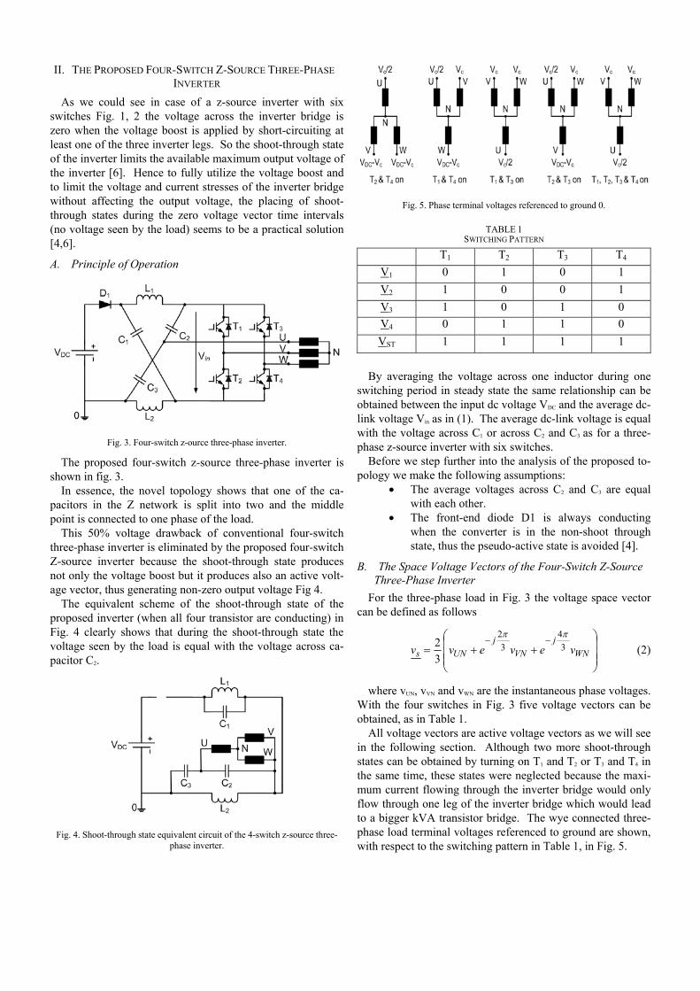
As we could see in case of a z-source inverter with six switches Fig. 1, 2 the voltage across the inverter bridge is zero when the voltage boost is applied by short-circuiting at least one of the three inverter legs. So the shoot-through state of the inverter limits the available maximum output voltage of the inverter [6]. Hence to fully utilize the voltage boost and to limit the voltage and current stresses of the inverter bridge without affecting the output voltage, the placing of shoot-through states during the zero voltage vector time intervals (no voltage seen by the load) seems to be a practical solution [4,6].
A. Principle of Operation
Fig. 3. Four-switch z-ource three-phase inverter.
The proposed four-switch z-source three-phase inverter is shown in fig. 3.
In essence, the novel topology shows that one of the ca-pacitors in the Z network is split into two and the middle point is connected to one phase of the load.
This 50% voltage drawback of conventional four-switch three-phase inverter is eliminated by the proposed four-switch Z-source inverter because the shoot-through state produces not only the voltage boost but it produces also an active volt-age vector, thus generating non-zero output voltage Fig 4.
The equivalent scheme of the shoot-through state of the proposed inverter (when all four transistor are conducting) in Fig. 4 clearly shows that during the shoot-through state the voltage seen by the load is equal with the voltage across ca-pacitor C2.
Fig. 4. Shoot-through state equivalent circuit of the 4-switch z-source three-phase inverter.
Fig. 5. Phase terminal voltages referenced to ground 0.
TABLE 1 SWITCHING PATTERN
T1 T2 T3 T4
V1 0 1 0 1 V2 1 0 0 1 V3 1 0 1 0 V4 0 1 1 0 VST 1 1 1 1
By averaging the voltage across one inductor during one
switching period in steady state the same relationship can be obtained between the input dc voltage VDC and the average dc-link voltage Vin as in (1). The average dc-link voltage is equal with the voltage across C1 or across C2 and C3 as for a three-phase z-source inverter with six switches.
Before we step further into the analysis of the proposed to-pology we make the following assumptions:
• The average voltages across C2 and C3 are equal with each other.
• The front-end diode D1 is always conducting when the converter is in the non-shoot through state, thus the pseudo-active state is avoided [4].
B. The Space Voltage Vectors of the Four-Switch Z-Source Three-Phase Inverter
For the three-phase load in Fig. 3 the voltage space vector can be defined as follows
⎟⎟⎟
⎠
⎞
⎜⎜⎜
⎝
⎛++=
−−WN
jVN
jUNs vevevv 3
43
2
32
ππ
(2)
where vUN, vVN and vWN are the instantaneous phase voltages. With the four switches in Fig. 3 five voltage vectors can be obtained, as in Table 1.
All voltage vectors are active voltage vectors as we will see in the following section. Although two more shoot-through states can be obtained by turning on T1 and T2 or T3 and T4 in the same time, these states were neglected because the maxi-mum current flowing through the inverter bridge would only flow through one leg of the inverter bridge which would lead to a bigger kVA transistor bridge. The wye connected three-phase load terminal voltages referenced to ground are shown, with respect to the switching pattern in Table 1, in Fig. 5.

In order to derive the phase voltages we will consider
2
; 321C
CCCCVVVVV === (3)
where 1CV , 2CV and 3CV are the average voltages across C1, C2 and C3 capacitors. For a symmetrical balanced wye con-nected three-phase load (Fig. 3) the phase voltages can be written as
( )
( )
( )000
000
000
31
32
31
32
31
32
VUWWN
UWVVN
WVUUN
vvvv
vvvv
vvvv
+−=
+−=
+−=
(4)
Substituting 0Uu , 0Vu and 0Wu , from fig. 5, into (4) and using the expression of the space voltage vector (2) the five voltage vectors can be derived as
CST
DCC
C
DCC
DCC
VV
VjVjV
VV
VjVjV
VVV
31
33
31
332
3131
33
31
332
31
32
4
3
2
1
−=
⎟⎟⎠
⎞⎜⎜⎝
⎛+−+⎟
⎟⎠
⎞⎜⎜⎝
⎛−=
−=
⎟⎟⎠
⎞⎜⎜⎝
⎛−−+⎟
⎟⎠
⎞⎜⎜⎝
⎛+=
−=
(5)
The relationship between the average capacitor voltage CV and the input dc voltage DCV can be expressed as
DCC VkV ⋅= (6)
1;21
1>
−−
= kD
DkST
ST (7)
Rewriting (5) using (7) the voltage vectors can be derived as
( ) ( )
( ) ( )
DCST
DC
DC
DC
DC
kVV
VkjkV
kVV
VkjkV
VkV
31
12331
3131
12331
31
32
4
3
2
1
−=
⎥⎥⎦
⎤
⎢⎢⎣
⎡+−+−=
−=
⎥⎥⎦
⎤
⎢⎢⎣
⎡−+−=
⎟⎠⎞
⎜⎝⎛ −=
(8)
Fig. 6. Locations of the voltage vectors in the complex plane.
Notice that in (8) the boost factor k influences the ampli-tude as well the direction of the six voltage vectors.
For k=2 the six voltage vectors in the complex plane are il-lustrated in fig. 6.
The voltage vector generated by the shoot-through state VST has the same amplitude and direction as the V3 voltage vector.
The voltage space vector expressed in (2) can be rewritten in the complex plane as
βα sss jvvv += (9)
The average voltage space vector over one switching cycle should be equal with the sum of the five average voltage space vectors (V1…V4 and VST) over one switching cycle Ts
( ) sSTSTs TVtVtVtVtVtv /44332211 ++++= (10)
where
sST Tttttt =++++ 4321 (11)
To obtain the expressions of αsv and βsv (9) the expres-sions of the five voltage vectors (8) are introduced in (10)
( ) ( )( ) ( )[ ]
( )( )1233
1233
42
3421
−−=
+−−++−=
kttTVv
kttkttktT
Vv
s
DCs
STs
DCs
β
α
(12)
Given (1)-(12) in this section it is possible to derive several algorithms that can be implemented in a digital signal proces-sor which, for a prescribed input space voltage vector,
∗∗∗ += βα sss jvvv (13)
calculate the duty ratios for the four transistors and generates the four gating pulses.

III. SHOOT-THROUGH PULSE IMPLEMENTATION AND PWM SIGNAL GENERATION
One easy way to generate the gating signals for the four transistors is to use three synchronized PWM units in com-plementary mode of a DSP with some additional circuitry.
Fig. 7. Block diagram of the PWM signal generation implementation.
Two of the three PWM generation units yield the two com-plementary signals for the two phase legs of the inverter bridge based on the prescribed duty ratios DV and DW. The third PWM unit generates the ST signal from DST. The four outputs from the two units are ORed with the ST signal thus obtaining the PWM signals for T1…T4.
Fig. 8. PWM signal waveform generation for T1, T2, T3 & T4.
IV. SIMULATION RESULTS In the first step of the validation, the proposed four-switch
z-source three-phase inverter was simulated in PSIM. The circuit parameters were as follows
kHzf
HzfkVv
RRFCCuFCmHLLVV
s
s
LL
DC
10
50;2;60
9.0;470;235;4.6;90
2132
121
=
===
Ω========
∗∗∗
μ
A three-phase wye connected RL load was used with the following parameters
mHLmHLmHL
RRR
WVU
WVU7.17;4.18;1.20
;2.10;6.10;5.10===
==Ω=
Only open loop performance with imposed output voltage vector amplitude, to derive commutation sequences and the required shoot-through time for the dc-link voltage boost, was investigated both in simulations and experiments.
The simulated waveforms are shown in Fig. 9-Fig. 13.
0 0.1 0.2 0.3 0.4 0.5-4
-3
-2
-1
0
1
2
3
4
Time [s]
Cur
rent
[A]
Fig. 9.Simulated load currents at start-up.
0.24 0.25 0.26 0.27 0.28 0.29 0.3 0.31-5
-4
-3
-2
-1
0
1
2
3
4
5
Time [s]
Cur
rent
[A]
IV
IU
IW
Fig. 10. Simulated load currents (zoom).

0 0.1 0.2 0.3 0.4 0.520
40
60
80
100
120
140
160
180
200
Time [s]
Vol
tage
[V]
VC1
VC3
VC2
VDC
Fig. 11. Simulated voltage waveforms across C1, C2, C3 and the input dc volt-age at start-up.
0 0.05 0.1 0.15 0.2 0.25 0.3 0.35-0.5
00.5
11.5
22.5
33.5
44.5
55.5
66.5
7
Time [s]
Cur
rent
[A]
IL1
IL2
Fig. 12. Simulated z-impedance inductor current waveforms IL1 and IL2.
0 0.1 0.2 0.3 0.4 0.50
50
100
150
200
250
300
Time [s]
Vol
tage
[V]
Fig. 13. Simulated instantaneous dc-link voltage Vi.
The shoot-through time was linearly increased from 0 to its nominal value in 0.120s to avoid the high inrush current Fig. 11. In Fig. 10 it can be seen that the load currents are not perfectly symmetrical due to the connection of phase U to the common node of capacitors C2 and C3 which causes the volt-age potential at this terminal to vary around 2CV Fig. 11.
The simulated inductor currents (which flow through both inverter legs during shoot-through states) are shown in Fig.
12, and they are less than 150% the peak load currents (Fig. 10). The boost dc-link voltage is shown in Fig. 13 (input dc voltage is 90V dc).
V. EXPERIMENTAL WORK A laboratory setup was built to experimentally validate the
proposed four-switch Z-source three-phase inverter. The con-trol algorithm based on equations (1)-(12) was implemented on a dsPIC30f3010 digital signal processor from Microchip with a clock frequency of 120MHz. The experimental wave-forms are shown in. Fig. 14-Fig.18.
The laboratory setup data are the same as for the digital simulations.
The experimental load currents in Fig. 14 are close to those from digital simulations (in Fig. 10) though a bit more asym-metric. The inverter starting experimental transients of Fig. 15-17 are similar to those obtained for same transients by digital simulations in Fig. 11 and 9 respectively.
The test and simulation load phase current transients (Fig. 17 and Fig. 9) fit rather well; the same observation is valid for VC2, VC3 which pulsate around input dc voltage of 90V dc. The dc-link (boosted) voltage VC1 in experiments (Fig. 15) pulsates around 160V while in simulation is around 180V dc, while the experimental inductor currents (Fig. 18) are smaller than the digital simulations (Fig. 12). These discrepancies require further insight.
0 0.01 0.02 0.03 0.04 0.05 0.06 0.07-5
-4
-3
-2
-1
0
1
2
3
4
5
Time [s]
Cur
rent
[A]
IW
IVI
U
Fig 14. Experimental load currents.
0 0.05 0.1 0.15 0.2 0.25 0.3 0.350
102030405060708090
100110120130140150160170180190200
Time [s]
Vol
tage
[V]
VC3
VC1
Fig. 15. Experimental voltages across C1 and C3 capacitors at start-up.

0 0.05 0.1 0.15 0.2 0.25 0.3 0.350
10
20
30
40
50
60
70
80
90
100
Time [s]
Vol
tage
[V]
VC2
VC3
Fig. 16. Experimental voltages across C2 and C3 capacitors at start-up.
0 0.05 0.1 0.15 0.2 0.25 0.3 0.35-4
-3
-2
-1
0
1
2
3
4
Time [s]
Cur
rent
[A]
IPhaseU
Fig. 17. Experimental current waveform through phase U at start-up.
0 0.05 0.1 0.15 0.2 0.25 0.3 0.35-0.5
00.5
11.5
22.5
33.5
44.5
55.5
66.5
7
Time [s]
Cur
rent
[A] I
L1
IL2
Fig. 18. Experimental Z-impedance inductor current waveforms IL1 and IL2.
VI. CONCLUSIONS This paper has proposed a novel four switch z-source three
-phase inverter topology which links together the advantages of a four switch inverter (low switch count) and a z-source inverter (self-boost ability). The shoot-through state not only boosts the input dc voltage but also produces an active volt-age as well, while in case of the z-source inverter with six switches the shoot-through state only boosts the input dc volt-age. By voltage-boost, the new four-switch z-source three-phase inverter eliminates the need to redesign the electric motor in terms of terminal voltage, as needed for conven-tional four-switch split capacitor three-phase inverters. The equations of the new converter were derived and the theory was verified through digital simulations and experiments.
ACKNOWLEDGEMENT This work was partially supported by the European Eco-
nomic Area (EEA) project RO 018 “Improvement of the Structures and Efficiency of Small Horizontal Axis Wind Generators with Non-Regulated Blades”.
REFERENCES [1] F. Z. Peng, “Z-source inverter”, IEEE Transactions on Industry Appli-
cations, Vol. 39, March-April 2003, pp.504-510. [2] Mauricio Beltrao de Rossiter Correa, Cursino Brandao Jacobina, Edison
Roberto Cabral da Silva, Antonio Marcus Nogueria Lima, “A General PWM Strategy for Four-Switch Three-Phase Inverters”, IEEE Transac-tions on Power Electronics, Vol. 21, November 2006, pp.1618-1627.
[3] Boldea Ion, Robert Antal, Muntean Nicolae “Modified Z-Source Sin-gle-Phase Inverter with Two Switches”, Proc. ISIE 2008, pp.257-263.
[4] Miaosen Shen, Fang Z. Peng, “Operation Modes and Characteristics of the Z-Source Inverter with Small Inductance”, IEEE Transactions on Power Electronics, Vol. 55, January 2008, pp.89-96.
[5] Poh Chiang Loh, Na Duan, Chao Liang, Feng Gao, Frede Blaabjerg, “Z-Source B4 Inverters”, Proc. PESC 2007, pp.1363-1369.
[6] Fang Z. Peng, Miaosen Shen, Zhaoming Qian, “Maximum Boost Con-trol of the Z-Source Inverter”, Proc. PESC 2004, pp.255-260.
[7] Feng Gao; Poh Chiang Loh; Blaabjerg, F.; Vilathgamuwa, D.M, “Per-formance Evaluation of Three-Level Z-Source Inverters Under Semi-conductor-Failure Conditions”, IEEE Transactions on Industry Applica-tions, Vol. 45, May-June 2009 pp.971-981.