Notice for the USA - ELHVB for the USA Compliance Information Statement (Declaration of Conformity...
72
Notice for the USA Compliance Information Statement (Declaration of Conformity Proce- dure) DoC FCC Part 15: This Device complies with Part 15 of the FCC Rules. Operation is subject to the following conditions: 1) this device may not cause harmful interference, and 2) this device must accept any interference received including interfer- ence that may cause undesired operation. If this equipment does cause harmful interference to radio or television reception, which can be determined by turning the equipment off and on, the user is encouraged to try one or more of the following measures: • Reorient or relocate the receiving antenna. • Increase the separation between the equipment and receiver. • Plug the equipment into an outlet on a circuit different from that of the receiver. • Consult the dealer or an experienced radio/television technician for help. Notice for Canada This apparatus complies with the Class B limits for radio interference as specified in the Canadian Department of Communications Radio Interference Regulations. Cet appareil est conforme aux normes de Classe B d’ interference radio tel que spécifié par le Ministére Canadien des Communications dans les réglements d’interférence radio. Notice for Europe (CE Mark) This product is in conformity with the Council Directive 89/336/EEC, 92/31/EEC (EMC).
Transcript of Notice for the USA - ELHVB for the USA Compliance Information Statement (Declaration of Conformity...

Notice for the USACompliance Information Statement (Declaration of Conformity Proce-dure) DoCFCC Part 15: This Device complies with Part 15 of the FCC Rules.Operation is subject to the following conditions:1) this device may not cause harmful interference, and2) this device must accept any interference received including interfer-ence that may cause undesired operation. If this equipment does causeharmful interference to radio or television reception, which can bedetermined by turning the equipment off and on, the user is encouragedto try one or more of the following measures:
• Reorient or relocate the receiving antenna.• Increase the separation between the equipment and receiver.• Plug the equipment into an outlet on a circuit different from
that of the receiver.• Consult the dealer or an experienced radio/television
technician for help.
Notice for CanadaThis apparatus complies with the Class B limits for radio interferenceas specified in the Canadian Department of Communications RadioInterference Regulations.
Cet appareil est conforme aux normes de Classe B d’ interferenceradio tel que spécifié par le Ministére Canadien des Communicationsdans les réglements d’interférence radio.
Notice for Europe (CE Mark)This product is in conformity with the Council Directive 89/336/EEC,92/31/EEC (EMC).

Table of Contents1. Introduction....................................................................... 4
Overview..................................................................... 4Icons........................................................................... 5Hardware Specifications/Features................................. 6Software Specifications.................................................9Technical Support......................................................... 9Returning Merchandise for Service................................ 10
2. Board Installation.............................................................. 12Unpacking....................................................................12Installation....................................................................13Setting Jumpers............................................................ 13
3. Onboard Resource Settings.............................................. 14Quick References for Jumpers...................................... 14Map of Motherboard Jumpers....................................... 15Soft Power Connector...................................................19Sleep Button Connector.................................................19Speaker Connector Installation...................................... 19External SMI................................................................19Hardware Reset Switch Connector Installation............... 20CMOS RTC................................................................. 20Flash EEPROM........................................................... 21Hardware CMOS & Password Reset............................ 21DRAM Installation....................................................... 21Installing the CPU........................................................ 23Peripheral Device Installation........................................ 28Connecting the Power Supply........................................ 28Frequently Asked Questions.......................................... 30
4. BIOS Configuration........................................................... 32Standard Setup............................................................. 32BIOS Features Setup.................................................... 34Advanced Setup........................................................... 35Chipset Setup............................................................... 40Power Management Setup............................................ 49PCI/PnP Setup............................................................. 52Peripheral Setup........................................................... 55Flash Writer Utility........................................................ 58

5. System Resources............................................................. 60POST Checkpoint Codes.............................................. 60Beep Codes................................................................. 68Troubleshooting System Problems.................................. 69Displayed Error Messages............................................ 70Additional Manuals....................................................... 72

4
Overview
The Thunder 2 (S1696DLUA) is a quality, high performancemotherboard designed for Intel’s latest generation of Pentium IImicroprocessors. This motherboard utilizes Intel’s 440LX AGP serieschipset (also called AGPset) and supports Pentium II CPU speeds of233MHz to 300MHz.
The Thunder 2 mainboard with built-in AGP slot provides high perfor-mance capabilities that are ideal for a wide range of demanding appli-cations such as CAD, CAM, CAE, desktop publishing, 3D animation,and video production. The Thunder 2 is suitable as a powerful worksta-tion, internet, intranet, file, network, and database server. The Thunder2’s superior dual processor technology increases performance andproductivity drastically for multi-processor enabled operating systemssuch as Microsoft Windows NT, Novell Netware SMP, and SCO Unix.
This integrated system board achieves high reliability with numerousfeatures. Some of the features included are onboard dual channel PCIUltraDMA 33, built-in Adaptec AIC7895 two channel ultra-wide SCSIand a third narrow SCSI, built-in Yamaha 16-bit OPL3-SA3 and OPL4-
Chapter 1
chap
ter 1
Introduction

5
INT
RO
ML wavetable and 3D sound chips, onboard floppy controller, andonboard high speed I/O.
The Thunder 2 board is built to be both flexible and expandable. WithI/O and drive controller support built onboard, the four 32-bit PCI BUSMaster and two ISA slots (one shared, six usable) are available foradd-on expansion cards.
Icons
In order to help you navigate this manual and set up your system, wehave added several icons to our format.
This icon alerts you to particularly important details regardingthe setup or maintenance of your system. This icon oftenappears next to information that may keep you from damag-
ing your board or system. While we will often point out the most vitalparagraphs in a chapter, you should always read every word in the text.Failing to do so can lead to exasperation and expense.
Wherever possible, we have included step-by-step instructionsfor setting up your system, which are indicated by this icon.However, it is in your best interest to read an entire section
(and perhaps the entire manual) before you begin to alter the settingson your motherboard.
While we have alerted you to potential dangers in severalplaces in this manual with this icon, these warnings should notbe regarded as the whole of your safety regimen. Never
forget that computers are electrical devices, and are capable of deliver-ing a burn or shock. Prevent damage to yourself and to your board:always ensure that your system is turned off and unplugged wheneveryou are working with it, and that you are equipped with a static safetydevice.
!

6
Hardware Specifications/Features
Processor Information sPentium II 233-300 MHz.sTwo SEC slots (Slot One).s2 VRM components installedonboard.s3 onboard CPU fan connectors.sIntel MPS v1.4 compliant.
Chipset Information sIntel 440LX AGPset.sIntel 82371AB(PIIX4).sIntel 82093 I/O APIC chip.
Voltage and Power sATX power supply connector.Information s+12 V power source for DC fan
onboard.s3.3V DRAM support.sUtilizes GTL+ BUS, reducing powerconsumption and EMI.sPower recovery after interrupt.sBulit-in overload protection thatautomatically shuts down the systemin case of power surge.
Main Memory sUp to 1024MB EDO or 512MBSDRAM onboard.sFour 168-pin DIMM slots.sEDO or SDRAM support.sECC support.
System Management sWake-on LAN 3-pin connector forremote booting by NetworkAdministrator.sOnboard National LM75 chip forCPU temperature sensing.
Chapter 1

7
sOnboard National LM78 thermalcontrol chip for heat, fan, and voltage.Reports to the operating system forsystem monitoring. LANdeskcompatible.sIntel LANDesk Client Managersoftware, and/or Intel LANDeskServer Manager software (with LM78installed).
Expansion Slots sOne AGP slot for 3D graphics card(supports 1x and 2x).sFour 32-bit PCI BUS Master slots.sTwo 16-bit ISA slots.sOne shared, six usable.
Physical Dimensions sIntel ATX design.s9.75 x 12 inches.sDouble-row ATX connectors.
BIOS Information sAMI Plug and Play flash BIOS.sDeep Green and Energy Starcompliant.sACPI, Year 2000, and PC97/98ready; PCI 2.1 compliant.sSoft power-down, multiple bootoptions.sWin98 Ready, DMI 2.0 compliant.sSupport for easy BIOS upgrades withflash EEPROM chip.
IDE Disk Drive & sTwo PCI BUS Mastering EIDESystem I/O channels.
sSupports EIDE CD-ROMs.sPIO Mode 3 & 4 (up to 17MB/secDTR).
INT
RO
8
Chapter 1
sUltraDMA 33 BUS Mastering Mode(up to 33MB/sec DTR).sTwo floppy drives (up to 2.88MB).sTwo ATX serial ports (16550UARTs).sOne ATX ECP/EPP parallel port.sOne IR (InfraRed) I/O interfaceport.sTwo USB rev 1.2 (universal serialBUS) ports.sOne ATX PS/2 mouse port.sOne ATX PS/2 keyboard connector.
SCSI Disk Controller sOnboard two channel Adaptec AIC-7895 Ultra-Wide SCSI controller(equivalent to Adaptec 3940AUW).sTwo Ultra-Wide channels withsynchronous 40MB/s DTR. Connectup to fifteen 16-bit devices perchannel (thirty devices total). Up toseven of the fifteen devices can be 8-bit devices.sOne Narrow channel with 20MB/sDTR.sBuilt-in RISC sequencer automatesSCSI protocol. Supports 32-bit BUSmaster DMA transfer.sRAID 0, 1, and 5 function built-inwith optional RAIDport card installed.
Sound Chip Information sOnboard Yamaha OPL3-SA3advanced 16-bit FM-synthesizer.sOnboard Yahama OPL4-MLadvanced wavetable with GeneralMIDI and MPU401 support.s44 voice wavetable synthesis in 1MBof wavetable ROM.

9
sSound Blaster Pro and WindowsSound System compatible.sPlug and Play with full duplexoperation.sBuilt-in 3D stereo sound and powermanagement.sOne game joystick port, one line-input, speaker output, and onemicrophone input.
Software Specifications
Operating System sOperates with MS-DOS, Windows3.x, Windows for WorkGroups 3.x,Windows 95, Windows NT, OS/2,Novell Netware, Solaris, and SCOUnix.
Technical Support
If a problem arises with your system, you should first turn to yourdealer for help. Your system has most likely been configured by them,and they should have the best idea of what hardware and software yoursystem contains. Hence, they should be able to be of the most assis-tance. Further, if you purchased your system from a dealer near to you,you can actually bring your system in to them to have it serviced,instead of attempting to yourself (which can have expensive conse-quences).If your dealer is unable to assist you:Try our web page – http:// www.tyan.com,or user newsgroup – alt.comp.periphs.mainboard.tyan.
INT
RO

10
Chapter 1
Returning Merchandise for Service
During the warranty period, contact your distributor or system vendorFIRST for any product problems. This warranty only covers normalcustomer use and does not cover damages incurred during shipping orfailure due to the alteration, misuse, abuse, or improper maintenance ofproducts.
For Resellers Only:A receipt or copy of your invoice marked with the date of purchase isrequired before any warranty service can be rendered. You can obtainservice by calling the manufacturer for a Return Merchandise Authori-zation (RMA) number. The RMA number should be prominentlydisplayed on the outside of the shipping carton and the package shouldbe mailed prepaid, or hand-carried to the manufacturer. Shipping andhandling charges will be applied for all orders that must be mailed whenservice is complete.
TrademarksAMI BIOS/Flash are trademarks of American Megatrend Inc.Windows is a trademark of Microsoft Corporation.IBM, PC, AT, PS/2 are trademarks of IBM Corporation.INTEL, Pentium II are trademarks of Intel Corporation.S1696DLUA Thunder 2 is a trademark of TYAN ComputerCorporation.All other trademarks are the property of their respective companies.
DisclaimerInformation presented in this publication has been carefully checkedfor reliability. However, no responsibility is assumed for inaccuracies.The information contained in this document is subject to changewithout notice.

11
This page has been left blank intentionally.
INT
RO

12
chap
ter 2
Board Installation
Unpacking
The mainboard package should contain the following:S1696DLUA mainboardOne IDE 40-pin cableOne 34-pin floppy cableOne 50-pin narrow SCSI cableOne 68-pin wide SCSI cableOne Thunder 2 user’s manualOne SCSI and sound appendix package (appendices A, B, and C)Two retention modules
The mainboard contains sensitive electric components which can beeasily damaged by static electricity, so the mainboard should be left inits original packaging until it is ready to be installed.
With the power supply plugged in and turned off, touch an unpaintedarea of the system chassis immediately before handling the mainboardor any component. Doing so discharges any static charge your bodymay have acquired.
Chapter 2

13
After opening the mainboard carton, extract the system board–holdingit by its edges–and place it on a grounded anti-static surface, compo-nent side up. Inspect the board for damage. Press down on any of thesocket ICs if it appears that they are not properly seated (the boardshould still be on an anti-static mat). Do not touch the bottom of theboard.
DO NOT APPLY POWER TO THE BOARD IF IT HAS BEENDAMAGED!
Installation
You are now ready to install your mainboard. The mounting holepattern of the S1696DLUA matches the ATX system board specifica-tions. Your chassis should be that of a standard ATX mainboard formfactor.
Setting Jumpers
In this manual, the terms “closed” and “on” are used when referring tojumpers (or jumper pins) that are active; “open” and “off” are usedwhen referring to jumpers (or jumper pins) that are not connected.Jumpers and pins are connected by slipping the black plastic jumperconnector overtop of two adjacent jumper pins. The metal rod insidethe plastic shell bridges the gap between the two pins, completing thecircuit. See the pictures below for examples of “on” and “off” pins andjumpers.
!
2 pin jumpers
off on
3 (or more) pin jumpers
1-2 2-3 open123
123
123
INS
TA
LL
14
Quick References for Jumpers
The following tables will help you set the jumpers for CPU speed, memoryvoltage settings, and SCSI PCI-ID, among others. The miniaturemotherboard maps will help you locate the jumpers on your board. A full-page map of the motherboard can be found on page 15.
Chapter 3
chap
ter 3
Onboard Resource Settings

15
ON
BO
AR
D
The tiny “1”s next to jumpers of 3 pins or more indicate the position ofpin 1 for that jumper. Refer to pages 16-18 for jumper and pin assign-ments.
Map of Motherboard Jumpers
3 volt lithium battery
Intel82371AB chip
Intel82443LX chip
ATX power connector
DIM
M B
ank
0
DIM
M B
ank
1
DIM
M B
ank
2
DIM
M B
ank
3
AdaptecAIC-7895P
chip
Pentium II CPU Slot 2
Pentium II CPU Slot 1
W. SCSI CH II
W. SCSI CH I
N. SCSISecondary IDEPrimary IDE
Floppy
10
13
18
2224
1
3
8
JP36
J25
JP23
FAN3
JP2
JP33
JP4
SCSI RAID Slot
ISA Slot 1
ISA Slot 2
PCI Slot 4
PCI Slot 3
PCI Slot 2
PCI Slot 1
JP7JP8JP9
JP10
JP3
J36J35
J37J34
J32J30
J31J33
FAN
1
JP34
JP32JP30A
JP31
JP41JP42
JP21
FAN
2
J40J38J39
J20
JP22
1
1 1
11
11
1
1
1
1
1
1
1
1
1
1
1
1
AGP (Accelerated Graphics Port)
Joys
tick
CO
M2
CO
M1
Prin
ter P
ort
USB
1
Mouse
Key
boar
d
LM75 chip
LM75 chip
LM78 chip
USB2
Line
inM
icro
phon
e in
Spea
ker o
ut

16
Flash BIOS
1 2 3
JP21 (Wake-on LAN) Standby 5V GND Wake (Power-on Active High)
FAN1-FAN3 GND VCC Fan Monitor
Pin Assignments
(-- indicates pin is absent)
Chapter 3
LM78 440LXbuilt-in dual VRM
RAID port
Ultra-Wide SCSINarrow SCSI
PCI ID
EFloppy
PIIX 4 Built-in currentoverload protection
SCSI LED
Adaptec AIC-7895Ultra-Wide SCSI chip
LM75
AG
P sl
otY
amah
a 16
-bit
3D s
ound
chi
p
OPL4-ML wavetable chipNat
iona
l Sup
erI/O
chi
p
APIC (Advanced ProgrammableInterrupt Controller) for multiprocessor
17
ON
BO
AR
D
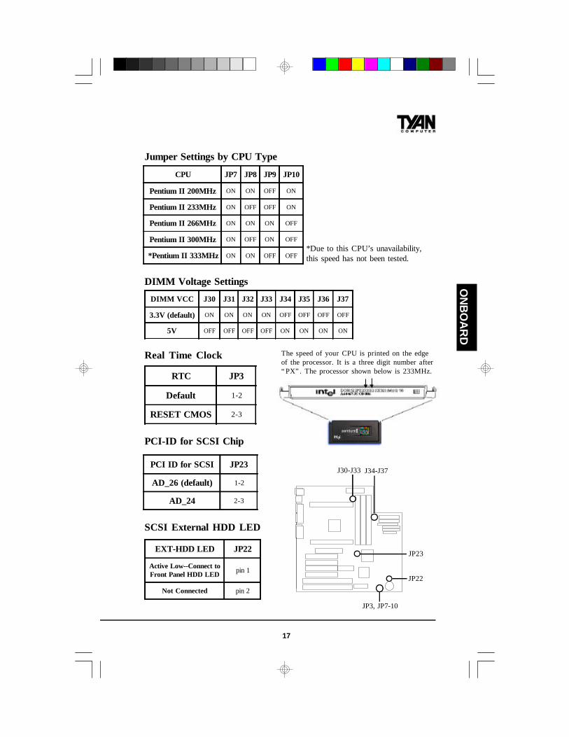
CPU JP7 JP8 JP9 JP10
Pentium II 200MHz ON ON OFF ON
Pentium II 233MHz ON OFF OFF ON
Pentium II 266MHz ON ON ON OFF
Pentium II 300MHz ON OFF ON OFF
*Pentium II 333MHz ON ON OFF OFF
Jumper Settings by CPU Type
DIMM Voltage Settings
Real Time Clock
PCI-ID for SCSI Chip
SCSI External HDD LED
DIMM VCC J30 J31 J32 J33 J34 J35 J36 J37
3.3V (default) ON ON ON ON OFF OFF OFF OFF
5V OFF OFF OFF OFF ON ON ON ON
RTC JP3
Default 1-2
RESET CMOS 2-3
PCI ID for SCSI JP23
AD_26 (default) 1-2
AD_24 2-3
JP3, JP7-10
JP23
J30-J33 J34-J37
JP22
EXT-HDD LED JP22
Active Low--Connect toFront Panel HDD LED pin 1
Not Connected pin 2
The speed of your CPU is printed on the edgeof the processor. It is a three digit number after“PX”. The processor shown below is 233MHz.
*Due to this CPU’s unavailability,this speed has not been tested.

18
Reserved
COM2/InfraRed Settings
SCSI Termination Settings CMOS Voltage Settings
Chapter 3
J25 Settings
Reserved
JP2 OPEN
JP38 Hardwired ON
JP39 Hardwired ON
JP40 OFF
JP48 OPEN
Pins 1-2 3-4 6-11 13-16 18-20 22-23 24-27
Function PowerOn/Off Sleep IR
Connector HDD LED PowerLED Reset Speaker
Assignment1=PowerOn/Off2=GND
3=GND4=Sleep
6=VCC7=NC
8=IR RX9=GND
10=IR TX11=Mode
13=VCC14=NC15=-16=+
18=GND19=NC20=+
22=GND23=Reset
24=VCC25=NC
26=INT-SPK27=-
J25
JP2JP38-JP40
JP41-JP42
COM2 IR
JP41 1-2 2-3
JP42 1-2 2-3
JP45 ON OFF
JP46 OFF ON
Pins Assignment
CH. A
JP43 1-2 SCSI high byte termination: all on (default)
2-3 Termination control by SCSI chip
CH. B
JP44 1-2 SCSI high byte termination: all on (default)
2-3 Termination control by SCSI chip
JP4
5V (default) 1-2
12V 2-3
19
Soft Power Connector
The Soft Power Connector is located on pins 1 and 2 of jumper blockJ25. Pressing the Soft Power Button will turn the system on (and off).
Sleep Button Connector
The sleep button connector is located on pin 3 and pin 4 of jumper blockJ25. Pressing this button will put the system in Sleep or Suspend mode.Pressing it once more will wake up the system. The power LED willblink when the system is in Sleep mode.
A four second override feature is built into the motherboard according toPC98 specifications. If you hold the sleep button for more than four sec-onds, the system will shut itself down. Use the four second override fea-ture when the system hangs or crashes. This feature is not intended fornormal shutdown operation. Please use the regular soft power button fora normal shutdown.
Speaker Connector Installation
The S1696DLUA provides a 4-pin header to connect the speaker. Thespeaker is connected to pins 24-27 of jumper block J25.
External SMI
The external SMI is located at jumper JP47. The pin assignment ispin1: external SMI; pin 2: GND.
ON
BO
AR
D

20
Hardware Reset Switch ConnectorInstallation
The Reset switch on your case’s display panel provides you with theHardware Reset function, which is the same as power on/off. Thesystem will do a cold start after the Reset button is pushed. The Resetswitch is a 2-pin connector and should be installed on pins 22 and 23 ofjumper block J25.
Windows 95 Users:You may encounter problems with some of the devices in the Intel82371AB chipset. Neither the PCI Bridge nor the PCI Universal SerialBUS device IDs for this chipset (also called PIIX4) are recognized byWindows 95. This is a software problem, not a hardware problem, andcan be easily remedied by either upgrading to Windows 98 or download-ing the 82371AB patch found at http://www.tyan.com or at ftp://download.intel.com/design/pcisets/busmastr/setupex.exe. (Note: USB re-quires Windows 95 OSR 2.1 or above; please contact Microsoft for theUSB update.)
CMOS RTC
The 440LX AGPset includes aninternal battery and Real TimeClock circuit. The RTC providesthe date and time for the system.If the battery is low, it will preventyour system from POSTing, andyou will not get a display. Nor-mally the life span of an RTCinternal battery is 10 years, but ifyours is running low, you will needto replace it with a new 3Vlithium battery (DuracellDL2032).
Chapter 3
J25
batteryJP3
!

21
Flash EEPROM
The S1696DLUA uses flash memory to store BIOS programs. It canbe updated as new versions of the BIOS become available. You canupgrade your BIOS easily using the flash utility (see page 58).
JP4 determines which type of EPROM is used. This jumper has beenset to match the onboard BIOS chip. The factory default for theS1696DLUA is on pins 1-2. Depending on the type of EPROM used,some boards will have JP4 on pins 2-3.
Hardware CMOS & Password Reset
If you have been locked out of your system because you forgot yourpassword or set the CMOS incorrectly, follow the instructions below.
1. Power off the system2. Set jumper JP3 to pins 2 and 3 (see previous page for location of JP3).3. Wait for 2 seconds, then return jumper JP3 to pins 1 and 2.4. Power on the system again.
By following this procedure, you will erase your password and reset theCMOS to the BIOS defaults.
DRAM Installation
The S1696DLUA uses a 64-bit data path from memory to CPU andcan accommodate up to 1024MB of EDO RAM and 512MB ofSDRAM. SDRAMs (Synchronous DRAMs) are supported in theDIMM slots. DIMMs must be of the unbuffered variety. The positionof the notch in the DRAM Key Position will tell you whether or not aDIMM is unbuffered (see figure on the next page). All installedmemory will be automatically detected, so there is no need to setjumpers. The 440LX AGPset can cache up to 512MB of RAM.
ON
BO
AR
D

22
Chapter 3
Some details of memory installation:s One unbuffered DIMM must be installed for the system to POST.s The mainboard supports 8MB, 16MB, 32MB, 64MB, 128MB
(SDRAM), and 256MB (EDO only) DIMM modules.
The table below shows some of the possible memory configurations.
* Maximum for SDRAM. ^Maximum for EDO.
DIMM Bank 0 DIMM Bank 1 DIMM Bank 2 DIMM Bank 3 Total
16MBx1 0 0 0 16MB
16MBx1 16MBx1 0 0 32MB
32MBx1 0 0 0 32MB
16MBx1 16MBx1 16MBx1 0 48MB
32MBx1 32MBx1 0 0 64MB
64MBx1 0 0 0 64MB
32MBx1 32MBx1 32MBx1 0 96MB
16MBx1 16MBx1 32MBx1 32MBx1 96MB
32MBx1 32MBx1 32MBx1 32MBx1 128MB
64MBx1 64MBx1 0 0 128MB
64MBx1 64MBx1 64MB 64MBx1 256MB
128MBx1 128MBx1 128MBx1 128MBx1 *512MB
256MBx1 256MBx1MBx1 256MBx1 256MBx1 ^1024MB
RFUBuffered
Unbuffered 168-pin DIMM
23
Installing the CPU
Pentium II processors (233 through 300MHz) can be used on theS1696DLUA. Please refer to page 15 for the correct CPU jumper set-tings for your board. Although the S1696DLUA motherboard is designedas a dual CPU system, it will also function with a single CPU.
The S1696DLUA board provides two slots for Pentium II processors,called the Pentium II primary and secondary slots. If only one CPU isused, that CPU should be plugged into the primary slot. When two CPUsare used, they should be of the same speed and type.
Remember:s The CPU is a sensitive electronic component and it can easily be
damaged by static electricity. Do not touch the CPU pins with yourfingers.
s When installing the CPU into the socket, match the CPU pins tothe socket pins. Note that one corner of the socket’s top is differentfrom the other three corners. Likewise, one corner of the CPU’sbottom is different from the other three corners. Line the uniquesocket corner up with the unique CPU corner.
s Before the CPU is installed, the mainboard must be placed on a flatsurface. You should be able to insert the CPU with minimal, butfirm, pressure. Do not press down hard on the CPU.
Active and Passive Processors
Currently, Intel produces two types of Pentium II processors: the active(or boxed) processor and the passive processor (refer to the pictures onthe following page). These two types of processors are essentially thesame in design; the only difference lies in their cooling methods. Theactive processor is equipped with a cooling fan and heat sink, while thepassive processor is equipped with a heat sink alone. Both types ofCPUs provide the user with the same performance, and both types canbe installed in the Pentium II slots on the S1696DLUA board. Refer topage 24 for instructions regarding the installation and removal ofPentium II processors.
ON
BO
AR
D!

24
Installation of Pentium II Active (Boxed) Processors
Active processors are equipped with cooling fans. When installing anactive CPU, you also need to connect the cooling fan cable to itsconnector.
Installing CPU Retention Modules
1. Installation of a Pentium II active processor requires a CPUretention module, which is first secured onto the motherboard. (Refer tothe motherboard layout on Page 16.)
2. To attach the retention module,place the motherboard on a flatsurface.
3. Locate the key pin on one end ofthe Pentium II slot on the board.Then carefully line up the key notchon the retention module with the keypin on the Pentium II slot (the key pinon the Pentium II slot indicates thecorrect orientation of the CPU).
Chapter 3
Pentium II Slot Connectorand Key Pin
Pentium II Active (Boxed) CPUShown with Power Connector for Fan
Pentium II Passive CPUShown with Heat-sink

25
4. Drop the retention module down over thePentium II slot so that the retention modulesits flat against the motherboard. Tighten thescrews in a clockwise manner to secure themodule to the board. Warning: Do not over-tighten the screws as you may damage themodule and/or the motherboard.
Installing the Active Processor
1. When the retention module is securelyinstalled, you are ready to plug the CPU intothe retention module.
2. Press firmly on the CPU until you hear a“click.” This clicking sound indicates that theCPU is fully locked into the retention mod-ule.3. After the CPU is securely seated on theretention module in the Pentium II slot, con-nect the CPU’s cooling fan cable to the cool-ing fan power connector on the board.
Installing CPU Cooling Fans
1. Locate the cooling fan connectors (3 connectors: FAN1-FAN3) on themotherboard.
2. Plug the CPU’s cooling fan cable into the cooling fan connector onthe board. Make sure that the black wire of the cable is plugged intopin 1 of the connector. Refer to pin 1 marked on the layout on page 16.Pin assignments: pin 1–ground (black), pin 2–12 V (red), pin 3– signal(yellow).
Retention Module
ON
BO
AR
D
Pentium II CPU enteringretention module

26
Installation of Pentium II Passive Processors
Unlike active processors, passive processors are not equipped withcooling fans. Instead, they are equipped with heat sinks.
Each CPU package should containthe following:One CPU retention moduleOne heat sink retention bracket withmounting locksTwo mounting attach-mountsOne heat sink lock
Installing CPU Retention Modules
1. When installing the CPU retention module, make sure that you havethe appropriate end of the module lined up with the key notch on thePentium II slot connector. This will ensure that the module is installedproperly.
2. Before tightening the screws, make certain that the module is flushagainst the motherboard. If one end of the module is raised above theboard, check the orientation of the module.
3. Install the module on the board by turning the screws in a clockwisedirection. Do not over-tighten the screws.
Installing Heat Sink Mounting Brackets
1. The heat sink mount hastwo pins on the bottom andfour pins on the top. Noticethat the bottom two pins areof different sizes. The sizeof the pins and the holes inthe motherboard will determine the correct orientation. A correctly
Chapter 3
Heat Sink MountingBracket
Pentium II PassiveCPU Module

27
Mounting Locks
installed bracket can be verified by making sure that the four pins onthe top are closest to the Pentium II CPU slot.
2. Insert the heat sink mount into the holes onthe motherboard. When the bracket is prop-erly inserted into the holes on themotherboard, you will hear a clicking noise.
3. Lock the heat sink mount to the board byinserting the two mounting locks into the pinsof the heat sink mounting bracket which arenow below the mainboard. There will be aclick when the locks are securely fastened.
Installing the Passive Processor
1. Align the CPU with the CPU retention module. Make sure the heatsink is lined up with the heat sink mount bracket. If you put the CPU inthe wrong way, you may damage the CPU, the motherboard, and/or theCPU socket.
2. Slowly press down on the CPU module until the CPU locks intoplace. A clicking noise will be heard when the CPU is locked securelyinto the module.
Installing Heat Sink Locks
The heat sink lock has four notches which will correspond to the fourpins on the heat sink mounting bracket. Gently slide the lock betweenthe heat sink onto the heatsink mounting bracket untilboth sides of the lock arefirmly secured. A clickingsound will be heard when thelock is securely fastened tothe heat sink mounting bracket. To remove the lock from the heat sinkmounting bracket, gently press the ends of the locks inward and pull.
ON
BO
AR
D
Heat Sink Lock

28
Chapter 3
Removing Pentium II Passive Processors and CPU RetentionModules
To remove the CPU, move the locks to the center of the CPU. A clickwill be heard when the CPU has been unlocked. Gently pull up on theCPU, taking care not to bend the motherboard or the CPU retentionmodule.
Removing Heat Sink Locks
To remove the lock from the retention bracket, gently press the ends ofthe locks inward and pull.
Peripheral Device Installation
After all the jumpers on the mainboard have been set, the mainboardcan be mounted into the case. You may then install the display card andany other peripheral devices that you may have.
If a PCI-BUS interface card is to be installed in the system, any one ofthe four PCI-BUS slots can support either a Master or a Slave device.
After installing the peripheral controllers, you should check the CPUand all of your devices again before preparing to power on the system.
Connecting the Power Supply
The female power supply connector on the mainboard fits with themale power supply connector from a 3.3V, 5V, or 12V power supply.Beware: incorrect installation of the power supply can result in seriousdamage to the system board and connected peripherals. Before con-necting the leads from the power supply, you should first make surethat the power supply is unplugged.
!

29
ON
BO
AR
D
Onboard connector
Power supply connector
tab
clip
Most male power supply connectors will have twenty wires, seven ofwhich are black. The black wires will be in the middle of the connector.The easiest way to orient the connectors properly is to line up theplastic clip on the male connector with the tab on the female connector.The plastic clip should be facing the edge of the motherboard.
Align the plastic guide pins on the male connector with their receptacleson the mainboard. You may need to hold the lead at an angle in order toproperly line it up with the onboard connector. Once you have the guidepins aligned, press the lead into the connector so that the plastic clip onthe lead snaps into place and secures the lead to the connector. Pleasesee the figure below.
30
Frequently Asked Questions
Q: Why don’t I get a display after I put in my old DIMM module?A: The 440LX chipset requires the memory manufacturer to programan EEPROM chip with SPD (Serial Presence Detection) on themodule in order for the BIOS to program the 440LX’s timing registersproperly. Your DIMM may not have the EEPROM chip on the module,or the EEPROM may not contain the correct program. Check withyour memory vendor for details. The figure below shows a DIMMmodule with an EEPROM chip.
Q: My system sometimes becomes unstable. How should I check thesystem?A: The first thing to do is to check and see if you have any deviceconflict in address, IRQ, or DMA. If you are using Windows 95, theDevice Manager is a good place to start. Please consult your operatingsystem manual for detail. Second of all, slowing down the memorytiming in the BIOS’s chipset setup section will help the situation, aswell. Many memory modules are not suitable for high performancesystems and are probably the main source of your problem.
Q: I’ve installed Windows NT with one CPU and with the multiproces-sor kernel. However, when I add a second CPU later, only one CPU isdetected during the Windows NT boot up.A: AMI BIOS only builds multiprocessor tables according to thenumber of CPUs present during Windows NT installation. Therefore,you must either reinstall NT with two CPUs or use the Windows NTresources kit to change from a uniprocessor to a multiprocessorsystem.
Chapter 3
RFUBuffered
Unbuffered 168-pin DIMM
EEPROM

31
Q: How do I know if the system detects the number of CPUsproperly?A: The AMI BIOS will show a “Pentium–II x2” message during thememory check to indicate the presence of two CPUs.
Q: How many devices can I hook up to each SCSI channel?A: You can cascade up to fifteen 16-bit devices per channel and sevenof them can be 8-bit devices.
Q: How do I use the RAID port on my motherboard?A: The RAID port allows you to put in an Adaptec Array 1000 familycard, which will enable the SCSI chip on the motherboard to performthe RAID function under Netware and Windows NT. RAID 0 is usedfor performance purposes (increases SCSI speed), RAID 1 is used formirroring (creates two drives with identical information), and RAID 5 isused for redundancy (if one drive goes down, another will take itsplace).
Q: Can I mix EDO DIMM with SDRAM DIMM on this motherboard?A: Yes. However, the AGP graphics card performs better withSDRAM installed on the motherboard because the AGP card can storethe texture map in the system memory.
Q: What is AGP (Accelerated Graphics Port)?A: AGP (Accelerated Graphics Port) is a new BUS architecture for3D graphics. The AGP slot eliminates the PCI bandwidth bottleneck bybypassing the PCI interface and accessing the system memory directly.Currently, the AGP supports 1X and 2X which yields bandwidths of264MB/s at 33MHz and 533MB/s at 66MHz BUS speeds, respectively.Compare with 132MB/s at 33MHz bus speed with PCI bus.
Q: Does my operating system support AGP?A: Currently, only Windows 98 and Windows NT 5.0 will have built-insupport for AGP. Some AGP cards require Windows 95 OSR2.1 or aspecial driver from Intel. Please check with your graphics vendor formore detail.
ON
BO
AR
D

32
Chapter 4
chap
ter 4
BIOS Configuration
Standard Setup
Select the AMIBIOS Setup options below by choosing Standard Setupfrom the AMIBIOS Setup main menu. Standard Setup options aredescribed below.
Floppy Drive A: and B:Move the cursor to these fields via the arrow keys and select the floppytype. The settings are 360KB 5¼ inch, 1.2 MB 5¼ inch, 720KB 3½inch, 1.44MB 3½ inch, or 2.88MB 3½ inch.
Primary Master, Primary Slave, Secondary Master, SecondarySlaveSelect these options to configure the drive named in the option. SelectAuto Detect IDE to let AMIBIOS automatically configure the drive. Ascreen with a list of drive parameters appears. Click on OK to config-ure the drive.

33
Entering Drive ParametersYou can also enter the hard disk drive parameters yourself. The driveparameters are as follows:
BIO
S
Type How to Configure
SCSISelect Type. Select Not Installed on the drive parameter screen. TheSCSI drivers provided by the SCSI manufacturer should allow you toconfigure the SCSI drive.
IDE
Select Type. Select Auto to let AMIBIOS determine the parameters.Click on OK when AMIBIOS displays the drive parameters. SelectLBA Mode. Select On if the drive has a capacity greater than540MB.Select Block Mode. Select On to allow block mode data transfers.Select 32-Bit Mode. Select On to allow 32-bit data transfers. Selectthe PIO Mode. It is best to select Auto to allow AMIBIOS todetermine the PIO mode. If you select a PIO mode that is notsupported by the IDE drive, the drive will not work properly. If youare absolutely certain that you know the drive's PIO mode, select PIOmode 0-4, as appropriate.
CD-ROM Select Type. Select CDROM. Click on OK when AMIBIOS displaysthe drive parameters.
Standard MFM Select Type. You must know the drive parameters. Select the drivetype that exactly matches your drive's parameters.
Non-Standard MFMSelect Type. If the drive parameters do not match the driveparameters listed for drive types 1-46, select User and enter thecorrect hard disk drive parameters.
Parameter Description
Type The number for a drive with certain identification parameters.
Cylinders The number of cylinders in the disk drive.
Heads The number of heads.
Write Precompensation
The actual physical size of a sector gets progressively smaller as thetrack diameter diminishes. Yet each sector must still hold 512 bytes.Write precompensation circuitry on the hard disk compensates for thephysical difference in sector size by boosting the write current forsectors on inner tracks. This parameter is the track number on thedisk surface where write precompensation begins.
Landing Zone This number is the cylinder location where the heads normally parkwhen the system is shut down.
Sectors
The number of sectors per track. MFM drives have 17 sectors pertrack. RLL drives have 26 sectors per track. ESDI drives have 34sectors per track. SCSI and IDE drives have even more sectors pertrack.
CapacityThe formatted capacity of the drive is the number of heads times thenumber of cylinders times the number of sectors per track times 512(bytes per sector).

34
Chapter 4
Type Cylinders Heads WritePrecompensation
LandingZone Sectors Capacity
1 306 4 128 305 17 10 MB
2 615 4 300 615 17 20 MB
3 615 6 300 615 17 31 MB
4 940 8 512 940 17 62 MB
5 940 6 512 940 17 47 MB
6 615 4 65535 615 17 20 MB
7 462 8 256 511 17 31 MB
8 733 5 65535 733 17 30 MB
9 900 15 65535 901 17 112 MB
10 820 3 65535 820 17 20 MB
11 855 5 65535 855 17 35 MB
12 855 7 65535 855 17 50 MB
13 306 8 128 319 17 20 MB
14 733 7 65535 733 17 43 MB
16 612 4 0 663 17 20 MB
17 977 5 300 977 17 41 MB
18 977 7 65535 977 17 57 MB
19 1024 7 512 1023 17 60 MB
20 733 5 300 732 17 30 MB
21 733 7 300 732 17 43 MB
22 733 5 300 733 17 30 MB
23 306 4 0 336 17 10 MB
24 925 7 0 925 17 54 MB
25 925 9 65535 925 17 69 MB
26 754 7 754 754 17 44 MB
27 754 11 65535 754 17 69 MB
28 699 7 256 699 17 41 MB
29 823 10 65535 823 17 68 MB
30 918 7 918 918 17 53 MB
31 1024 11 65535 1024 17 94 MB
32 1024 15 65535 1024 17 128 MB
33 1024 5 1024 1024 17 43 MB
34 612 2 128 612 17 10 MB
35 1024 9 65535 1024 17 77 MB
36 1024 8 512 1024 17 68 MB
37 615 8 128 615 17 41 MB
38 987 3 987 987 17 25 MB
39 987 7 987 987 17 57 MB
40 820 6 820 820 17 41 MB
41 977 5 977 977 17 41 MB
511 981 5 981 981 17 41 MB
43 830 7 512 830 17 48 MB
44 830 10 65535 830 17 69 MB
45 917 15 65535 918 17 114 MB
46 1224 15 65535 1223 17 152 MB

35
BIO
S
Advanced Setup
The Advanced Setup options included in the AMIBIOS Setup gener-ated through AMIBCP and the AMIBIOS for the Intel 440LX chipsetare described in this chapter. Select Advanced Setup from theAMIBIOS Setup main menu to display the Advanced Setup options.
Default Settings
Every option in AMIBIOS Setup contains two default values: an Fail-Safe default and the Optimal default value.
Optimal DefaultsThe Optimal default values provide optimum performance settings forall devices and system features.
Fail-Safe DefaultsThe Fail-Safe default settings consist of the safest set of parameters.Use them if the system is behaving erratically. They should alwayswork but do not provide optimal system performance characteristics.
Advanced Setup
Quick BootSet this option to Enabled to instruct AMIBIOS to boot quickly whenthe computer is powered on. This option replaces the old Above 1 MBMemory Test Advanced Setup option. The settings are:
Setting Description
Disabled
AMIBIOS tests all system memory.AMIBIOS waits up to 40 seconds for a READY signal from the IDE hard disk drive. AMIBIOS waits for .5seconds after sending a RESET signal to the IDE drive to allow the IDE drive time to get ready again.AMIBIOS checks for a <Del> key press and runs AMIBIOS Setup if the key has been pressed.
Enabled
AMIBIOS does not test system memory above 1MB.AMIBIOS does not wait up to 40 seconds for a READY signal from the IDE hard disk drive. If a READY signalis not received immediately from the IDE drive, AMIBIOS does not configure that drive. AMIBIOS does notwait for .5 seconds after sending a RESET signal to the IDE drive to allow the IDE drive time to get ready again.You cannot run AMIBIOS Setup at system boot, because there is no delay for the Hit <Del> to run Setupmessage.
The Optimal and Fail-Safe default settings are Disabled.

36
Setting Description
BIOS The messages that AMIBIOS displays before booting the system will appear on the system monitor.
Silent The messages that AMIBIOS displays will not appear on the system monitor.
Chapter 4
1st Boot DeviceThis option sets the type of device for the first boot drives that theAMIBIOS attempts to boot from after AMIBIOS POST completes.The settings are Disabled, Network, Floptical, SCSI, CDROM, IDE-0,IDE-1, IDE-2, or IDE-3. The Optimal and Fail-Safe default settings areIDE-0.
2nd Boot DeviceThis option sets the type of device for the second boot drives that theAMIBIOS attempts to boot from after AMIBIOS POST completes.The settings are Disabled, Floppy, Floptical, CDROM, or IDE-0. TheOptimal and Fail-Safe default settings are Floppy.
3rd Boot DeviceThis option sets the type of device for the third boot drives that theAMIBIOS attempts to boot from after AMIBIOS POST completes.The settings are Disabled, Floptical, Floppy, CDROM, or IDE-0. TheOptimal and Fail-Safe default settings are CD-ROM.
Try Other Boot DevicesSet this option to Yes to instruct AMIBIOS to attempt to boot from anyother drive in the system if it cannot find a boot drive among the drivesspecified in the 1st Boot Device, 2nd Boot Device, and 3rd BootDevice options. The settings are Yes or No. The Optimal and Fail-Safedefault settings are Yes.
Initial Display ModeThis option specifies the initial display mode when the system boots.The settings are as follows:
37
Display Mode At Add-On ROM InitThis option specifies the system display mode that is set at the timethat AMIBIOS POST initializes an optional option ROM. The settingsare as follows:
Floppy Access ControlThis option specifies the read/write access that is set when bootingfrom a floppy drive. The settings are Read/Write or Read-Only. TheOptimal and Fail-Safe default settings are Read/Write.
Hard Disk Access ControlThis option specifies the read/write access that is set when bootingfrom a hard disk drive. The settings are Read/Write or Read-Only. TheOptimal and Fail-Safe default settings are Read/Write.
S.M.A.R.T. For Hard DisksSet this option to Enabled to permit AMIBIOS to use the SMART(System Management and Reporting Technologies) protocol forreporting server system information over a network. Enabling thisfeature allows you to back up your data when your hard disk is aboutto fail. The settings are Enabled or Disabled. The Optimal and Fail-Safe default settings are Disabled.
Boot Up Num LockSet this option to Off to turn the Num Lock key off when the computeris booted so you can use the arrow keys on both the numeric keypadand the keyboard. The settings are On or Off. The default settings areOn.
Setting Description
Force BIOS The display mode currently being used by AMIBIOS is used.
Keep Current The current display mode is used.
BIO
S

38
Chapter 4
PS/2 Mouse SupportSet this option to Enabled to enable AMIBIOS support for a PS/2-typemouse. The BIOS will allocate IRQ12 for the PS/2 mouse. The settingsare Enabled or Disabled. The Optimal and Fail-Safe default settingsare Enabled.
Primary DisplayThis option configures the type of monitor attached to the computer.The settings are Mono, CGA40x25, CGA80x25, VGA/EGA, orAbsent. The Optimal and Fail-Safe default settings are VGA/EGA.
Password CheckThis option enables password checking every time the system boots orwhen you run AMIBIOS Setup. If Always is chosen, a user passwordprompt appears every time the computer is turned on. If Setup ischosen, the password prompt appears if AMIBIOS is executed. See theAdvanced Setup chapter for instructions on changing a password. TheOptimal and Fail-Safe defaults are Setup.
Boot To OS/2Set this option to Enabled if running OS/2 operating system and usingmore than 64 MB of system memory on the motherboard. The settingsare Enabled or Disabled. The Optimal and Fail-Safe default settingsare Disabled.
CPU Microcode UpdateSet this option to Enabled to permit the BIOS to update the CPU at anytime. The settings are Enabled or Disabled. The Optimal and Fail-Safedefault settings are Enabled.
Internal CacheThis option sets the type of caching algorithm used by the L1 internalcache memory on the CPU. The settings are WriteBack, WriteThru, orDisabled. The Optimal and Fail-Safe default settings are Disabled.

39
System BIOS CacheableWhen set to Enabled, the contents of the F0000h system memorysegment can be read from or written to cache memory. The contents ofthis memory segment are always copied from the BIOS ROM tosystem RAM for faster execution. The settings are Enabled or Dis-abled. The Optimal default setting is Enabled. The Fail-Safe defaultsetting is Disabled.
C000,16K Shadow and C400,16K ShadowThese options specify how the 32 KB of video ROM at C0000h istreated. The settings are:
The Optimal and Fail-Safe default settings are Cached.
C800,16K Shadow; CC00,16K Shadow; D000,16K Shadow;D400,16K Shadow; D800, 16K Shadow; and DC00,16K ShadowThese options enable shadowing of the contents of the ROM areanamed in the option. The ROM area not used by ISA adapter cards isallocated to PCI adapter cards. The settings are:
The Optimal and Fail-Safe default settings are Cached.
BIO
S
Setting Description
Disabled The contents of the video ROM are not copied to RAM.
Enabled The contents of the video ROM area from C000h-C7FFFh are copied (shadowed) from ROM toRAM for faster execution.
Cached The contents of the video ROM area from C000h-C7FFFh are copied from ROM to RAM and canbe written to or read from cache memory.

40
Chapter 4
Chipset Setup
Choose Chipset Setup on the AMIBIOS Setup main menu. All ChipsetSetup options are then displayed. AMIBIOS Setup can be customized.AMIBIOS Setup can be customized via AMIBCP. See the AMIBIOSUtilities Guide for additional information.
USB FunctionSet this option to Enabled to enable USB (Universal Serial Bus)support. The settings are Enabled or Disabled. The Optimal and Fail-Safe default settings are Enabled.
USB Keyboard/Mouse Legacy SupportSet this option to Enabled to enable support for older keyboards andmouse devices if the USB Function option is set to Enabled. Thesettings are Enabled or Disabled. The Optimal and Fail-Safe defaultsettings are Disabled.
EDO DRAM Speed (ns) This option specifies the RAS Access Time in nanoseconds for theEDO DRAM system memory installed in this computer. The settingsare Auto (AMIBIOS automatically determines the RAS access Timeparameter), Manual, 50, 60, or 70. The Optimal and Fail-Safe defaultsettings are Auto.
EDO Read Burst TimingThis option specifies the timings for EDO DRAM system memory forRead operations in burst mode. The settings are x222 or x333. TheOptimal and Fail-Safe default settings are x333. Setting this switchincorrectly may result in system failure.
EDO Write Burst TimingThis option specifies the timings for EDO DRAM system memory forWrite operations in burst mode. The settings are x222 or x333. TheOptimal and Fail-Safe default settings are x333. Setting this switchincorrectly may result in system failure.

41
BIO
S
EDO RAS PrechargeThis option specifies the length of the RAS precharge part of theDRAM system memory access cycle when EDO DRAM systemmemory is installed in this computer. The settings are 3 CLKs or 4CLKs. The Optimal and Fail-Safe default settings are 4 CLKs.
EDO RAS To CASThis option specifies the length of the delay inserted between the RASand CAS signals of the DRAM system memory access cycle whenEDO DRAM system memory is installed in this computer. The settingsare 2 CLKs or 3 CLKs. The Optimal and Fail-Safe default settings are3 CLKs.
MA Wait StateThis option specifies the length of the delay inserted between MAsignals. The settings are Slow or Fast. The Optimal and Fail-Safedefault settings are Slow.
SDRAM Timing LatencyThis option specifies the latency for the Synchronous DRAM systemmemory signals. The settings are Auto (AMIBIOS automaticallydetermines the optimal delay) or Manual. The Optimal and Fail-Safedefault settings are Auto.
RAS To CASThis option specifies the length of the delay inserted between the RASand CAS signals of the DRAM system memory access cycle. Thesettings are 2 CLKs or 3 CLKs. The Optimal and Fail-Safe defaultsettings are 3 CLKs.
CAS Lat.This option sets the latency period for the CAS signal. The settings are2 CLKs or 3 CLKs. The Optimal and Fail-Safe default settings are 3CLKs.

42
Chapter 4
RAS PrechargeThis option specifies the length of the RAS precharge part of theDRAM system memory access cycle when EDO DRAM systemmemory is installed in this computer. The settings are 3 CLKs or 4CLKs. The Optimal and Fail-Safe default settings are 4 CLKs.
VGA Frame Buffer USWCSet this option to Enabled to enable the VGA video frame buffer usingUSWC (Uncacheable, Speculatable, Write-Combined) memory. Thesettings are Enabled or Disabled. Older ISA VGA card drivers may notbehave correctly if this option is not set to Disabled. The Optimal andFail-Safe default settings are Disabled.
PCI Frame Buffer USWCSet this option to Enabled to enable the USWC memory attribute andimprove video performance when a PCI video adapter is installed.However, some VGA card drivers may not behave correctly when thisoption is set to Enabled. The settings are Disabled or Enabled. TheOptimal and Fail-Safe defaults are Disabled.
DRAM Integrity ModeThis option sets the type of system memory checking. The settings are:
Setting Description
Non ECC No error checking or error reporting is done.
ECC Only
Multibit errors are detected and reported as parity errors. Single-bit errors arecorrected by the chipset. Corrected bits of data from memory are not written back toDRAM system memory. If Level I is selected, the J25 External SMI software jumperon the Series 745 board is disabled.
ECC
Multibit errors are detected and reported as parity errors. Single bit errors are correctedby the chipset and are written back to DRAM system memory. If a soft (correctable)memory error occurs, writing the fixed data back to DRAM system memory will resolvethe problem. If a hard (uncorrectable) error occurs, writing the fixed data back toDRAM system memory does not solve the problem. In this case, the second time theerror occurs in the same location, a parity error is reported, indicating an uncorrectableerror. If ECCI is selected, AMIBIOS automatically enables the System ManagementInterface (SMI). If you do not want to enable power management, set the PowerManagement/APM option to Disabled and set all Power Management Setup timeoutoptions to Disabled. To enable power management, set Power Management/APM toEnabled and set the Power Management Setup timeout options as desired.

43
BIO
S
Fixed Memory HoleThis option specifies the location of an area of memory that cannot beaddressed on the ISA bus. The settings are Disabled, 15 MB-16 MB, or512KB-640KB. The Optimal and Fail-Safe default settings are Dis-abled.
TypeF DMA BufferControl1 and TypeF DMA Buffer Control2These options specify the DMA channel where TypeF buffer control isimplemented. The settings are Disabled, Channel-0, Channel-1,Channel-2, Channel-3, Channel-5, Channel-6, or Channel-7. TheOptimal and Fail-Safe default settings are Disabled.
DMA-0 Type, DMA-1 Type, DMA-2 Type, DMA-3 Type, DMA-5Type, DMA-6 Type, DMA-7 TypeThese options specify the bus that the specified DMA channel can beused on. The settings are PC/PCI, Distributed, or Normal ISA. TheOptimal and Fail-Safe default settings are Normal ISA.
AGP Aperture SizeThis option specifies the amount of system memory that can be usedby the Accelerated Graphics Port (AGP). The settings are 4 MB, 8 MB,16 MB, 32 MB, 64 MB, 128 MB, or 256 MB. The Optimal and Fail-Safe default settings are 256 MB.
System TypeThis option sets the system type. The settings are Auto (AMIBIOSautomatically determines the system type), DP, or UP. The Optimaland Fail-Safe default settings are Auto.

44
Chapter 4
USWC Write I/O PostThis option sets the status of USWC posted writes to I/O. The settingsare:
The Optimal and Fail-Safe default settings are Auto.
MECC Buf. StrengthThis option sets the strength of the signal for the MECC buffer. Thesettings are Auto (AMIBIOS automatically determines the correctsetting), 42mA, 38mA, or 33mA. The Optimal and Fail-Safe defaultsettings are Auto.
MD Buf. StrengthThis option sets the strength of the signal for the MD buffer. Thesettings are Auto (AMIBIOS automatically determines the correctsetting), 42mA, 38mA, or 33mA. The Optimal and Fail-Safe defaultsettings are Auto.
WE Buf. StrengthThis option sets the strength of the signal for the WE buffer. Thesettings are Auto (AMIBIOS automatically determines the correctsetting), 42mA, 38mA, or 33mA. The Optimal and Fail-Safe defaultsettings are Auto.
MAX Buf. StrengthThis option sets the strength of the signal for the MAX buffer. Thesettings are Auto (AMIBIOS automatically determines the correctsetting), 42mA, 38mA, or 33mA. The Optimal and Fail-Safe defaultsettings are Auto.
MA Buf. StrengthThis option sets the strength of the signal for the MA buffer. The
Setting Description
Enabled USWC posted writes to I/O are enabled.
Disabled USWC posted writes to I/O are disabled.
Auto AMIBIOS automatically determines if USWC posted writes to I/O should be enabled and sets thisoption accordingly.

45
BIO
S
settings are Auto (AMIBIOS automatically determines the correctsetting), 48mA, 42mA, or 22mA. The Optimal and Fail-Safe defaultsettings are Auto.
SCAS3 Buf. StrengthThis option sets the strength of the signal for the SCAS3 buffer. Thesettings are Auto (AMIBIOS automatically determines the correctsetting), 48mA, 42mA, or 22mA. The Optimal and Fail-Safe defaultsettings are Auto.
SCAS2:0 Buf. StrengthThis option sets the strength of the signal for the SCAS2:0 buffer. Thesettings are Auto (AMIBIOS automatically determines the correctsetting), 42mA, 38mA, or 33mA. The Optimal and Fail-Safe defaultsettings are Auto.
SRAS3 Buf. StrengthThis option sets the strength of the signal for the SRAS3 buffer. Thesettings are Auto (AMIBIOS automatically determines the correctsetting), 48mA, 42mA, or 22mA. The Optimal and Fail-Safe defaultsettings are Auto.
SRAS2:0 Buf. StrengthThis option sets the strength of the signal for the SRAS2:0 buffer. Thesettings are Auto (AMIBIOS automatically determines the correctsetting), 48mA, 42mA, or 22mA. The Optimal and Fail-Safe defaultsettings are Auto.
DQMX5 Buf. StrengthThis option sets the strength of the signal for the DQMX5 buffer. Thesettings are Auto (AMIBIOS automatically determines the correctsetting), 42mA, 38mA, or 33mA. The Optimal and Fail-Safe defaultsettings are Auto.
DQMX1 Buf. StrengthThis option sets the strength of the signal for the DQMX1 buffer. Thesettings are Auto (AMIBIOS automatically determines the correct

46
Chapter 4
setting), 42mA, 38mA, or 33mA. The Optimal and Fail-Safe defaultsettings are Auto.
DQM Buf. StrengthThis option sets the strength of the signal for the DQM buffer. Thesettings are Auto (AMIBIOS automatically determines the correctsetting), 42mA, 38mA, or 33mA. The Optimal and Fail-Safe defaultsettings are Auto.
CSX Buf. StrengthThis option sets the strength of the signal for the CSX buffer. Thesettings are Auto (AMIBIOS automatically determines the correctsetting), 48mA, 42mA, or 22mA. The Optimal and Fail-Safe defaultsettings are Auto.
CS7:6 Buf. StrengthThis option sets the strength of the signal for the CS7:6 buffer. Thesettings are Auto (AMIBIOS automatically determines the correctsetting), 48mA, 42mA, or 22mA. The Optimal and Fail-Safe defaultsettings are Auto.
CS5:0 Buf. StrengthThis option sets the strength of the signal for the CS5:0 buffer. Thesettings are Auto (AMIBIOS automatically determines the correctsetting), 48mA, 42mA, or 22mA. The Optimal and Fail-Safe defaultsettings are Auto.
PAC Bus SERR#Set this option to Enabled to enable the SERR# signal on the PAC bus.The settings are Enabled or Disabled. The Optimal and Fail-Safedefault settings are Enabled.
AGP Common SERR#Set this option to Enabled to permit a common SERR# signal for AGPand the standard PC bus. The settings are Enabled or Disabled. TheOptimal and Fail-Safe default settings are Enabled.

47
BIO
S
AGP System Error ForwardingSet this option to Enabled to enable AGP system errors to be for-warded. The settings are Enabled or Disabled. The Optimal and Fail-Safe default settings are Enabled.
AGP Parity Error ResponseSet this option to Enabled to enable AGP parity error response. Thesettings are Enabled or Disabled. The Optimal and Fail-Safe defaultsettings are Enabled.
IRQ12This option specifies how IRQ12 is used. The settings are:
The Optimal and Fail-Safe default settings are Auto.
PIIX4 SERR#Set this option to Enabled to enable the SERR# signal for the IntelPIIX4 chip. The settings are Enabled or Disabled. The Optimal andFail-Safe default settings are Disabled.
USB Passive Release EnableSet this option to Enabled to enable passive release for USB. Thesettings are Enabled or Disabled. The Optimal and Fail-Safe defaultsettings are Disabled.
PIIX4 PassiveSet this option to Enabled to enable passive release for the Intel PIIX4chip. The settings are Enabled or Disabled. The Optimal and Fail-Safedefault settings are Enabled.
PIIX4 Delayed TransactionSet this option to Enabled to enable delayed transactions for the Intel
Setting Description
Auto AMIBIOS automatically determines how IRQ12 should be allocated.
Standard IRQ12 is made available for use on the ISA BUS.
Mouse IRQ12 is used by the PS/2 mouse.

48
Chapter 4
PIIX4 chip. The settings are Enabled or Disabled. The Optimal andFail-Safe default settings are Enabled.
Master Lat. TimerThis option specifies the latency for the Timer. The settings are 00hthrough F8h in increments of 08h. The settings are 00h.

49
BIO
S
Power Management Setup
The AMIBIOS Setup options described in this section are selected bychoosing Power Management Setup from the AMIBIOS Setup mainmenu.
ACPI Aware OSSet this option to Enabled to enable Advanced Configuration andPower Interface (ACPI) BIOS for an ACPI-aware operating system.
Power Management/APMSet this option to Enabled to enable the chipset power managementand APM (Advanced Power Management) features. The settings areEnabled or Disabled. The Optimal and Fail-Safe default settings areDisabled.
Power Button FunctionThis option specifies how the power button mounted externally on thecomputer chassis is used. The settings are:
The Optimal and Fail-Safe default settings are On/Off.
Instant On SupportSet this option to Enabled to enable AMIBIOS support for the IntelInstantON specification. The settings are Enabled or Disabled. TheOptimal and Fail-Safe default settings are Disabled.
Green PC Monitor Power StateThis option specifies the power state that the green PC-compliantvideo monitor enters when AMIBIOS places it in a power saving stateafter the specified period of display inactivity has expired. The settings
Setting Description
On/Off Pushing the power button turns the computer on or off.
Suspend Pushing the power button places the computer in Suspend mode or Full On power mode.

50
Chapter 4
are Off, Standby, Suspend, or Disabled. The Optimal and Fail-Safedefault settings are Disabled.
Video Power Down ModeThis option specifies the power state that the video subsystem enterswhen AMIBIOS places it in a power saving state after the specifiedperiod of display inactivity has expired. The settings are Standby,Suspend or Disabled. The Optimal and Fail-Safe default settings areDisabled.
Hard Disk Power Down ModeThis option specifies the power conserving state that the hard diskdrive enters after the specified period of hard drive inactivity hasexpired. The settings are Disabled, Standby, or Suspend. The Optimaland Fail-Safe default settings are Disabled.
Hard Disk Timeout (Minute)This option specifies the length of a period of hard disk drive inactiv-ity. When this length of time expires, the computer enters power-conserving state specified in the Hard Disk Power Down Mode option(see the previous page). The settings are Disabled, 1 min. (minute), 2min, 3 min., 4 min., 5 min., 6 min, 7 min., 8 min., 9 min., 10 min., 11min., 12 min., 13 min., 14 min, and 15 min. The Optimal and Fail-Safedefault settings are Disabled.
Standby/Suspend Timer UnitThis option specifies the unit of time used for the Standby and Sus-pend timeout periods. The settings are 4 msec, 4 sec, 32 sec, or 4 min.The Optimal and Fail-Safe default settings are 4 min.
Standby TimeoutThis option specifies the length of a period of system inactivity whilein Full power on state. When this length of time expires, the computerenters Standby power state. The settings are Disabled, 4 msec, 8 msec,12 msec, 16 msec, up to 508 msec, in increments of 4 msec. TheOptimal and Fail-Safe default settings are Disabled.

51
BIO
S
Suspend TimeoutThis option specifies the length of a period of system inactivity whilein Standby state. When this length of time expires, the computer entersSuspend power state. The settings are Disabled, 4 msec, 8 msec, 12msec, 16 msec, up to 508 msec, in increments of 4 msec. The Optimaland Fail-Safe default settings are Disabled.
Slow Clock RatioThis option specifies the speed at which the system clock runs in theStandby Mode power saving state. The settings are expressed as apercentage between the normal CPU clock speed and the CPU clockspeed when the computer is in the power-conserving state. The settingsare 0-12.5%, 12.5-25%, 25-37.5%, 37.5-50%, 50-62.5%, 62.5-75%, or75-87.5%. The Optimal and Fail-Safe default settings are 50-62.5%.
Display ActivityWhen set to Monitor, this option enables event monitoring on the videodisplay. If set to Monitor and the computer is in a power saving state,AMIBIOS watches for display activity. The computer enters the FullOn state if any activity occurs. AMIBIOS reloads the Standby andSuspend timeout timers if display activity occurs. The settings areMonitor or Ignore. The Optimal and Fail-Safe default settings areIgnore.
Device 6 (Serial Port 1), Device 7 (Serial Port 2), Device 8 (ParallelPort), Device 5 (Floppy Disk), Device 0 (Primary Master IDE),Device 1 (Primary Salve IDE), Device 2 (Secondary Master IDE),and Device 3 (Secondary Slave IDE)When set to Monitor, these options enable event monitoring on thespecified hardware interrupt request line. If set to Monitor and thecomputer is in a power saving state, AMIBIOS watches for activity onthe specified IRQ line. The computer enters the Full On state if anyactivity occurs. AMIBIOS reloads the Standby and Suspend timeouttimers if activity occurs on the specified IRQ line. The settings foreach of these options are Monitor or Ignore. The Optimal and Fail-Safedefault settings are Ignore.

52
Chapter 4
PCI/PnP Setup
Choose PCI/Plug and Play Setup from the AMIBIOS Setup screen todisplay the PCI and Plug and Play Setup options, described below.
Plug and Play Aware O/SSet this option to Yes to inform AMIBIOS that the operating systemcan handle plug and Play (PnP) devices. The settings are No or Yes.The Optimal and Fail-Safe default settings are No.
PCI Latency Timer (PCI Clocks)This option specifies the latency timings (in PCI clocks) for PCIdevices installed in the PCI expansion slots. The settings are 32, 64,96, 128, 160, 192, 224, or 248. The Optimal and Fail-Safe defaultsettings are 64.
PCI VGA Palette SnoopWhen this option is set to Enabled, multiple VGA devices operating ondifferent buses can handle data from the CPU on each set of paletteregisters on every video device. Bit 5 of the command register in thePCI device configuration space is the VGA Palette Snoop bit (0 isdisabled). For example, if there are two VGA devices in the computer(one PCI and one ISA) and this field is set for:
This option must be set to Enabled if any ISA adapter card installed inthe system requires VGA palette snooping. The Optimal and Fail-Safedefault settings are Disabled.
Allocate IRQ To PCI VGASet this option to Yes to allocate an IRQ to the VGA device on the PCIbus. The settings are Yes or No. The Optimal and Fail-Safe defaultsettings are Yes.
Setting Description
Disabled Data read and written by the CPU is only directed to the PCI VGA device's palette registers.
Enabled Data read and written by the CPU is directed to the both the PCI VGA device's palette registers andthe ISA VGA device palette registers, permitting the palette registers of both devices to be identical.

53
BIO
S
PCI IDE Bus MasterSet this option to Enabled to specify that the IDE controller on the PCIbus has bus mastering capability. The settings are Disabled or Enabled.The Optimal and Fail-Safe default settings are Disabled.
Offboard PCI IDE CardThis option specifies if an offboard PCI IDE controller adapter card isused in the computer. You must also specify the PCI expansion slot onthe motherboard where the offboard PCI IDE controller card is in-stalled. If an offboard PCI IDE controller is used, the motherboardonboard IDE controller is automatically disabled. The settings areDisabled, Auto, Slot1, Slot2, Slot3, Slot4, Slot5, or Slot6. If Auto isselected, AMIBIOS automatically determines the correct setting. TheOptimal and Fail-Safe default settings are Auto. This option forces IRQ14 and 15 to a PCI slot on the PCI local bus. This is necessary tosupport non-compliant PCI IDE adapter cards.
Offboard PCI IDE Primary IRQThis option specifies the PCI interrupt used by the primary IDEchannel on the offboard PCI IDE controller. The settings are Disabled,Hardwired, INTA, INTB, INTC, or INTD. The Optimal and Fail-Safedefault settings are Disabled.
Offboard PCI IDE Secondary IRQThis option specifies the PCI interrupt used by the secondary IDEchannel on the offboard PCI IDE controller. The settings are Disabled,Hardwired, INTA, INTB, INTC, or INTD. The Optimal and Fail-Safesettings are Disabled.
PCI Slot1 IRQ Priority, PCI Slot2 IRQ Priority, PCI Slot3 IRQPriority, and PCI Slot4 IRQ PriorityThese options specify the IRQ priority for PCI devices installed in thePCI expansion slots. The settings are Auto, (IRQ) 3, 4, 5, 7, 9, 10, and11, in order of priority. The Optimal and Fail-Safe default settings areAuto.

54
Chapter 4
DMA Channel 0, DMA Channel 1, DMA Channel 3, DMA Chan-nel 5, DMA Channel 6, and DMA Channel 7These options allow you to specify the bus type used by each DMAchannel. The settings are PnP or ISA/EISA . The Optimal and Fail-Safe default settings are PnP.
IRQ3, IRQ4, IRQ5, IRQ7, IRQ9, IRQ10, IRQ11, IRQ12, IRQ14,and IRQ15These options specify the bus that the specified IRQ line is used on.These options allow you to reserve IRQs for legacy ISA adapter cards.These options determine if AMIBIOS should remove an IRQ from thepool of available IRQs passed to devices that are configurable by thesystem BIOS. The available IRQ pool is determined by reading theESCD NVRAM. If more IRQs must be removed from the pool, theend user can use these options to reserve the IRQ by assigning an ISA/EISA setting to it. Onboard I/O is configured by AMIBIOS. All IRQsused by onboard I/O are configured as PCI/PnP. IRQ12 only appears ifthe Mouse Support option in Advanced Setup is set to Disabled. IRQ14and 15 will not be available if the onboard PCI IDE is enabled. If allIRQs are set to ISA/EISA and IRQ14 and 15 are allocated to theonboard PCI IDE, IRQ9 will still be available for PCI and PnP devices,because at least one IRQ must be available for PCI and PnP devices.The settings are ISA/EISA or PCI/PnP. The Optimal and Fail-Safedefault settings are PCI/PnP.
Reserved Memory Size This option specifies the size of the memory area reserved for legacyISA adapter cards. The settings are Disabled, 16K, 32K, or 64K. TheOptimal and Fail-Safe default settings are Disabled.
Reserved Memory AddressThis option specifies the beginning address (in hex) of the reservedmemory area. The specified ROM memory area is reserved for use bylegacy ISA adapter cards. This option does not appear if the ReservedMemory Size option is set to Disabled. The settings are C0000, C4000,C8000, CC000, D0000, D4000, D8000, or DC000. The Optimal andFail-Safe default settings are N/A.

55
BIO
S
Peripheral Setup
Peripheral Setup options are displayed by choosing Peripheral Setupfrom the AMIBIOS Setup main menu. All Peripheral Setup options aredescribed here.
Onboard FDC Set this option to Enabled to enable the floppy drive controller on themotherboard. The settings are Auto (AMIBIOS automatically deter-mines if the floppy controller should be enabled), Enabled, or Dis-abled. The Optimal and Fail-Safe default settings are Enabled.
Onboard Serial Port1 This option specifies the base I/O port address of serial port 1. Thesettings are Auto (AMIBIOS automatically determines the correct baseI/O port address), Disabled, 3F8h, 2F8h, 2E8h, or 3E8h. The Optimaland Fail-Safe default settings are Auto.
Onboard Serial Port2 This option specifies the base I/O port address of serial port 2. Thesettings are Auto (AMIBIOS automatically determines the correct baseI/O port address), Disabled, 3F8h, 2F8h, 2E8h, or 3E8h. The Optimaland Fail-Safe default settings are Auto.
Serial Port2 ModeThis option specifies the operating mode for serial port 2.This optiononly appears if the Onboard Serial Port2 option is not set to Auto orDisabled. The settings are IrDA, ASK IR, or Normal. The Optimal andFail-Safe default settings are Normal.
IR Transmission ModeThis option specifies the infrared transmission method. This optiononly appears if the Onboard Serial Port2 option is not set to Auto orDisabled. The settings are Full Duplex or Half Duplex. There are nodefault settings.

56
Chapter 4
Receiver PolarityThis option specifies if the IRQ signal for IR transmission is ActiveHigh or Active Low. The settings are Active High or Active Low. Thereare no default settings.
Transmitter PolarityThis option specifies if the IRQ signal for IR transmission is ActiveHigh or Active Low. The settings are Active High or Active Low. Thereare no default settings.
Onboard Parallel Port This option specifies the base I/O port address of the parallel port onthe motherboard. The settings are Disabled, 378h, 278h, or 3BCh. TheOptimal default setting is 378h. The Fail-Safe default setting is Dis-abled.
Parallel Port ModeThis option specifies the parallel port mode. The Optimal defaultsetting is Normal. The Fail-Safe default setting is Disabled. Thesettings are:
EPP VersionThis option specifies the Enhanced Parallel Port specification versionnumber that is used in the system. This option only appears if theParallel Port Mode option is set to EPP. The settings are 1.7 or 1.9.There are no Optimal and Fail-Safe default settings because the defaultsetting for the Parallel Port Mode option is not EPP.
Setting Description
Normal The normal parallel port mode is used.
Bi-Dir Use this setting to support bidirectional transfers on the parallel port.
EPPThe parallel port can be used with devices that adhere to the Enhanced Parallel Port(EPP) specifications. EPP uses the existing parallel port signals to provide asymmetricbidirectional data transfer driven by the host device.
ECPThe parallel port can be used with devices that adhere to the Extended Capabilities Port(ECP) specifications. ECP uses the DMA protocol to achieve data transfer rates of upto 2.5 Megabits per second. ECP provides symmetric bidirectional communication.

57
Parallel Port IRQThis option specifies the IRQ used by the parallel port. The settings areAuto, (IRQ) 5, or (IRQ) 7. The Optimal and Fail-Safe default settingsare Auto.
Parallel Port DMA ChannelThis option is only available if the setting for the Parallel Port Modeoption is ECP. This option sets the DMA channel used by the parallelport. The settings are DMA Channel 0, 1, or 3. The Optimal and Fail-Safe default settings are not provided.
Onboard IDEThis option specifies the IDE channel used by the onboard IDEcontroller. The settings are Disabled, Primary, or Secondary. TheOptimal and Fail-Safe default settings are Disabled.
Onboard SCSIThis option will enable or disable the onboard SCSI BIOS. The defaultsetting is Enabled.
Power InterruptionEnabling this option will allow the system to return to power on stagewhen interrupted by a power outage.
SoundThis option allows you to manually select an IRQ, address, and DMAnumber for the sound chip. The default setting is Auto.
Port Bar JoystickThis option enables or disables the game port connector onboard.
BIO
S

58
Chapter 4
Flash Writer Utility
The AMI Flash Writer Utility is now included in the AMIBIOS, and soit is simpler to upgrade the BIOS of your mainboard. The systemBIOS is stored on a flash EEPROM ROM chip on the mainboardwhich can be erased and reprogrammed by following the directionsbelow.
1. Rename the BIOS file that you have downloaded to “amiboot.rom”and copy it on to a floppy disk.2. Insert the floppy disk with the BIOS upgrade into the A: drive.3. Turn the power off.4. While holding the <Ctrl> and <Home> keys, turn the power on. Thesystem will begin to read from the A: drive, and write the BIOSinformation contained on the floppy disk in that drive to the EEPROMROM chip. When the BIOS has been totally reprogrammed, you willhear three beeps and the system will reboot with the new BIOS inoperation.5. If the system does not reboot in three minutes, power down thesystem, wait a few seconds, and then turn the power back on again.

59
BIO
S
This page has been left blank intentionally.

60
Chapter 5
POST Checkpoint Codes
When AMIBIOS performs the Power On Self Test, it writes diagnosticcodes (checkpoint codes) to I/O port 0080h. If teh computer cannotcomplete the boot process, diagnostic equipment can be attached to thecomputer to read I/O port 0080h. The following AMIBIOS POSTcheckpoint codes are valid for all AMIBIOS products with a coreBIOS date of 7/15/95 (Enhanced).
System Resources
chap
ter 5
61
Uncompressed Initialization CodesThe uncompressed initialization codes are listed in order of execution.
SY
ST
EM
Checkpoint Code Description
D0h The NMI is disabled. Power on delay is starting. Next, the initializationcode checksum will be verified.
D1h Initializing the DMA controller, performing the keyboard controller BATtest, starting memory refresh, and entering 4 GB flat mode next.
D3h Starting memory sizing next.
D4h Returning to real mode. Executing any OEM patches and setting thestack next.
D5hPassing control to the uncompressed code in shadow RAM atE000:0000h. The initialization code is copied to segment 0 and controlwill be transferred to segment 0.
D6h
Control is in segment 0. Next, checking if <Ctrl> <Home> waspressed and verifiying the system BIOS checksum. If <Ctrl> <Home>was pressed or the system BIOS checksum is bad, next will go tocheckpoint code E0h. Otherwise, going to D7h.
D7h Passing control to the interface module next.
D8h The main system BIOS runtime code will be decompressed next.
D9h Passing control to the main system BIOS in shadow RAM next.

62
Chapter 5
Bootblock Recovery CodesThe bootblock recovery checkpoint codes are listed in order of execu-tion.
Uncompressed Initialization CodesThe following routine checkpoint codes are listed in order of execu-tion. These codes are uncompressed in F000h shadow RAM. The tablebegins on the next page.
Checkpoint Code Description
E0h The onboard floppy controller if available is initialized. Next, beginningthe base 512 KB memory test.
E1h Initializing the interrupt vector table next.
E2h Initializing the DMA and Interrupt controllers next.
E6h Enabling the floppy drive controller and Timer IRQs. Enabling internalcache memory.
EDh Initializing the floppy drive.
EEh Looking for a floppy diskette in drive A:. Reading the first sector of thediskette.
EFh A read error occurred while reading the floppy drive in drive A:.
F0h Next, searching for the AMIBOOT.ROM file in the root directory.
F1h The AMIBOOT.ROM file is not in the root directory.
F2h Next, reading and analyzing the floppy diskette FAT to find the clustersoccupied by the AMIBOOT.ROM file.
F3h Next, reading the AMIBOOT.ROM file, cluster by cluster.
F4h The AMIBOOT.ROM file is not the correct size.
F5h Next, disabling internal cache memory.
FBh Next, detecting the type of flash ROM.
FCh Next, erasing the flash ROM.
FDh Next, programming the flash ROM.
FFh Flash ROM programming was successful. Next, restarting the systemBIOS.

63
Checkpoint Code Description
03h The NMI is disabled. Next, checking for a soft reset or a power oncondition.
05h The BIOS stack has been built. Next, disabling cache memory.
06h Uncompressing the POST code next.
07h Next, initializing the CPU and the CPU data area.
08h The CMOS checksum calculation is done next.
0Bh Next, performing any required initialization before the keyboard BATcommand is issued.
0Ch The keyboard controller input buffer is free. Next, issuing the BATcommand to the keyboard controller.
0EhThe keyboard controller BAT command result has been verified. Next,performing any necessary initialization after the keyboard controller BATcommand test.
0Fh The initialization after the keyboard controller BAT command test is done.The keyboard command byte is written next.
10h The keyboard controller command byte is written. Next, issuing the Pin 23and 24 blocking and unblocking commands.
11h
Next, checking if the <End or <Ins> keys were pressed during power on.Initializing CMOS RAM if the Initialize CMOS RAM in every bootAMIBIOS POST option was set in AMIBCP or the <End> key waspressed.
12h Next, disabling DMA controllers 1 and 2 and interrupt controllers 1 and 2.
13h The video display has been disabled. Port B has been initialized. Next,initializing the chipset.
14h The 8254 timer test will begin next.
19h The 8254 timer test is over. Starting the memory refresh test next.
1Ah The memory refresh line is toggling. Checking the 15 second on/off timenext.
23hReading the 8042 input port and disabling the MEGAKEY Green PCfeature next. Making the BIOS code segment writable and performing anynecessary configuration before initializing the interrupt vectors.
24h The configuration required before interrupt vector initialization hascompleted. Interrupt vector initialization is about to begin.
25h Interrupt vector initialization is done. Clearing the password if the POSTDIAG switch is on.
27h Any initialization before setting video mode will be done next.
28h Initialization before setting the video mode is complete. Configuring themonochrome mode and color mode settings next.
2Ah Bus initialization system, static, output devices will be done next, if present.See page 71 for additional information.
2Bh Passing control to the video ROM to perform any required configurationbefore the video ROM test.
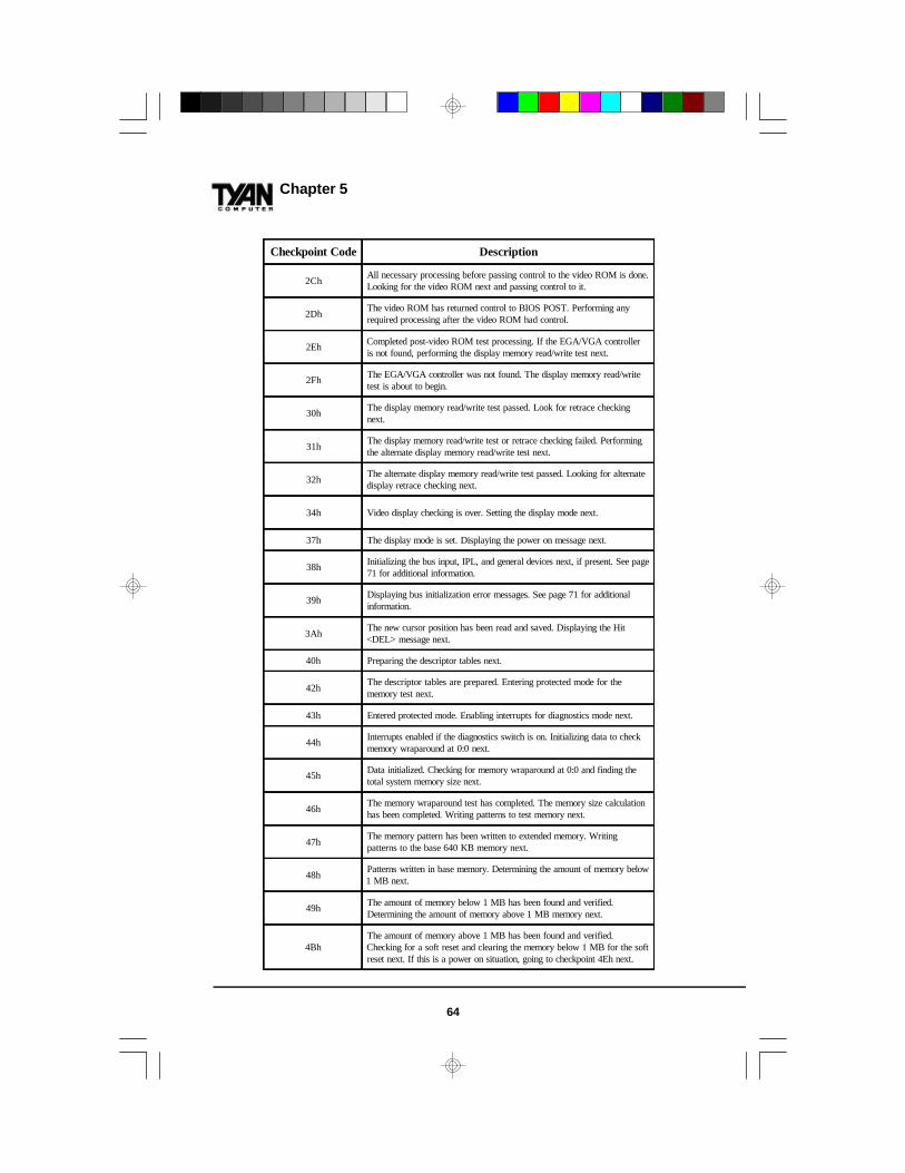
64
Chapter 5
Checkpoint Code Description
2Ch All necessary processing before passing control to the video ROM is done.Looking for the video ROM next and passing control to it.
2Dh The video ROM has returned control to BIOS POST. Performing anyrequired processing after the video ROM had control.
2Eh Completed post-video ROM test processing. If the EGA/VGA controlleris not found, performing the display memory read/write test next.
2Fh The EGA/VGA controller was not found. The display memory read/writetest is about to begin.
30h The display memory read/write test passed. Look for retrace checkingnext.
31h The display memory read/write test or retrace checking failed. Performingthe alternate display memory read/write test next.
32h The alternate display memory read/write test passed. Looking for alternatedisplay retrace checking next.
34h Video display checking is over. Setting the display mode next.
37h The display mode is set. Displaying the power on message next.
38h Initializing the bus input, IPL, and general devices next, if present. See page71 for additional information.
39h Displaying bus initialization error messages. See page 71 for additionalinformation.
3Ah The new cursor position has been read and saved. Displaying the Hit<DEL> message next.
40h Preparing the descriptor tables next.
42h The descriptor tables are prepared. Entering protected mode for thememory test next.
43h Entered protected mode. Enabling interrupts for diagnostics mode next.
44h Interrupts enabled if the diagnostics switch is on. Initializing data to checkmemory wraparound at 0:0 next.
45h Data initialized. Checking for memory wraparound at 0:0 and finding thetotal system memory size next.
46h The memory wraparound test has completed. The memory size calculationhas been completed. Writing patterns to test memory next.
47h The memory pattern has been written to extended memory. Writingpatterns to the base 640 KB memory next.
48h Patterns written in base memory. Determining the amount of memory below1 MB next.
49h The amount of memory below 1 MB has been found and verified.Determining the amount of memory above 1 MB memory next.
4BhThe amount of memory above 1 MB has been found and verified.Checking for a soft reset and clearing the memory below 1 MB for the softreset next. If this is a power on situation, going to checkpoint 4Eh next.

65
Checkpoint Code Description
4Ch The memory below 1 MB has been cleared via a soft reset. Clearing thememory above 1 MB next.
4Dh The memory above 1 MB has been cleared via a soft reset. Saving thememory size next. Going to checkpoint 52h next.
4Eh The memory test started, but not as the result of a soft reset. Displaying thefirst 64 KB memory size next.
4Fh The memory size display has started. The display is updated during thememory test. Performing the sequential and random memory test next.
50h The memory below 1 MB has been tested and initialized. Adjusting thedisplayed memory size for relocation and shadowing next.
51hThe memory size display was adjusted for relocation and shadowing.Testing the memory above 1 MB next.
52h The memory above 1 MB has been tested and initialized. Saving thememory size information next.
53h The memory size information and the CPU registers are saved. Enteringreal mode next.
54h Shutdown was successful. The CPU is in real mode. Disabling the GateA20 line, parity, and the NMI next.
57h The A20 address line, parity, and the NMI are disabled. Adjusting thememory size depending on relocation and shadowing next.
58h The memory size was adjusted for relocation and shadowing. Clearing theHit <DEL> message next.
59h The Hit <DEL> message is cleared. The <WAIT...> message is displayed.Starting the DMA and interrupt controller test next.
60h The DMA page register test passed. Performing the DMA Controller 1base register test next.
62h The DMA controller 1 base register test passed. Performing the DMAcontroller 2 base register test next.
65h The DMA controller 2 base register test passed. Programming DMAcontrollers 1 and 2 next.
66h Completed programming DMA controllers 1 and 2. Initializing the 8259interrupt controller next.
7Fh Extended NMI source enabling is in progress.
80h The keyboard test has started. Clearing the output buffer and checking forstuck keys. Issuing the keyboard reset command next.
81h A keyboard reset error or stuck key was found. Issuing the keyboardcontroller interface test command next.
82h The keyboard controller interface test completed. Writing the commandbyte and initializing the circular buffer next.
83h The command byte was written and global data initialization has completed.Checking for a locked key next.
SY
ST
EM

66
Chapter 5
Checkpoint Code Description
84h Locked key checking is over. Checking for a memory size mismatch withCMOS RAM data next.
85h The memory size check is done. Displaying a soft error and checking for apassword or bypassing WINBIOS Setup next.
86h The password was checked. Performing any required programming beforeWINBIOS Setup next.
87hThe programming before WINBIOS Setup has completed. Uncompressingthe WINBIOS Setup code and executing the AMIBIOS Setup orWINBIOS Setup utility next.
88h Returned from WINBIOS Setup and cleared the screen. Performing anynecessary programming after WINBIOS Setup next.
89h The programming after WINBIOS Setup has completed. Displaying thepower on screen message next.
8BhThe first screen message has been displayed. The <WAIT...> message isdisplayed. Performing the PS/2 mouse check and extended BIOS dataarea allocation check next.
8Ch Programming the WINBIOS Setup options next.
8Dh The WINBIOS Setup options are programmed. Resetting the hard diskcontroller next.
8Fh The hard disk controller has been reset. Configuring the floppy drivecontroller next.
91h The floppy drive controller has been configured. Configuring the hard diskdrive controller next.
95h Initializing the bus option ROMs from C800 next. See page 71 foradditional information.
96h Initializing before passing control to the adaptor ROM at C800.
97h Initialization before the C800 adaptor ROM gains control has completed.The adaptor ROM check is next.
98hThe adaptor ROM had control and has now returned control to BIOSPOST. Performing any required processing after the option ROM returnedcontrol.
99h Any initialization required after the option ROM test has completed.Configuring the timer data area and printer base address next.
9Ah Set the timer and printer base addresses. Setting the RS-232 base addressnext.
9Bh Returned after setting the RS-232 base address. Performing any requiredinitialization before the Coprocessor test next.
9Ch Required initialization before the Coprocessor test is over. Initializing theCoprocessor next.
9Dh Coprocessor initialized. Performing any required initialization after theCoprocessor test next.
9EhInitialization after the Coprocessor test is complete. Checking the extendedkeyboard, keyboard ID, and Num Lock key next. Issuing the keyboard IDcommand next.

67
Checkpoint Code Description
A2h Displaying any soft errors next.
A3h The soft error display has completed. Setting the keyboard typematic ratenext.
A4h The keyboard typematic rate is set. Programming the memory wait statesnext.
A5h Memory wait state programming is over. Clearing the screen and enablingparity and the NMI next.
A7h NMI and parity enabled. Performing any initialization required beforepassing control to the adaptor ROM at E000 next.
A8h Initialization before passing control to the adaptor ROM at E000hcompleted. Passing control to the adaptor ROM at E000h next.
A9h Returned from adaptor ROM at E000h control. Performing anyinitialization required after the E000 option ROM had control next.
AAh Initialization after E000 option ROM control has completed. Displaying thesystem configuration next.
ABh Building the multiprocessor table, if necessary.
ACh Uncompressing the DMI data and initializing DMI POST next.
B0h The system configuration is displayed.
B1h Copying any code to specific areas.
00h Code copying to specific areas is done. Passing control to INT 19h bootloader next.
The system BIOS passes control to different BUSes at thefollowing checkpoints:
Checkpoint Code Description
2Ah Initializing the different bus system, static, and output devices, if present.
38h Initialized bus input, IPL, and general devices, if present.
39h Displaying bus initialization error messages, if any.
95h Initializing bus adaptor ROMs from C8000h through D8000h.
SY
ST
EM
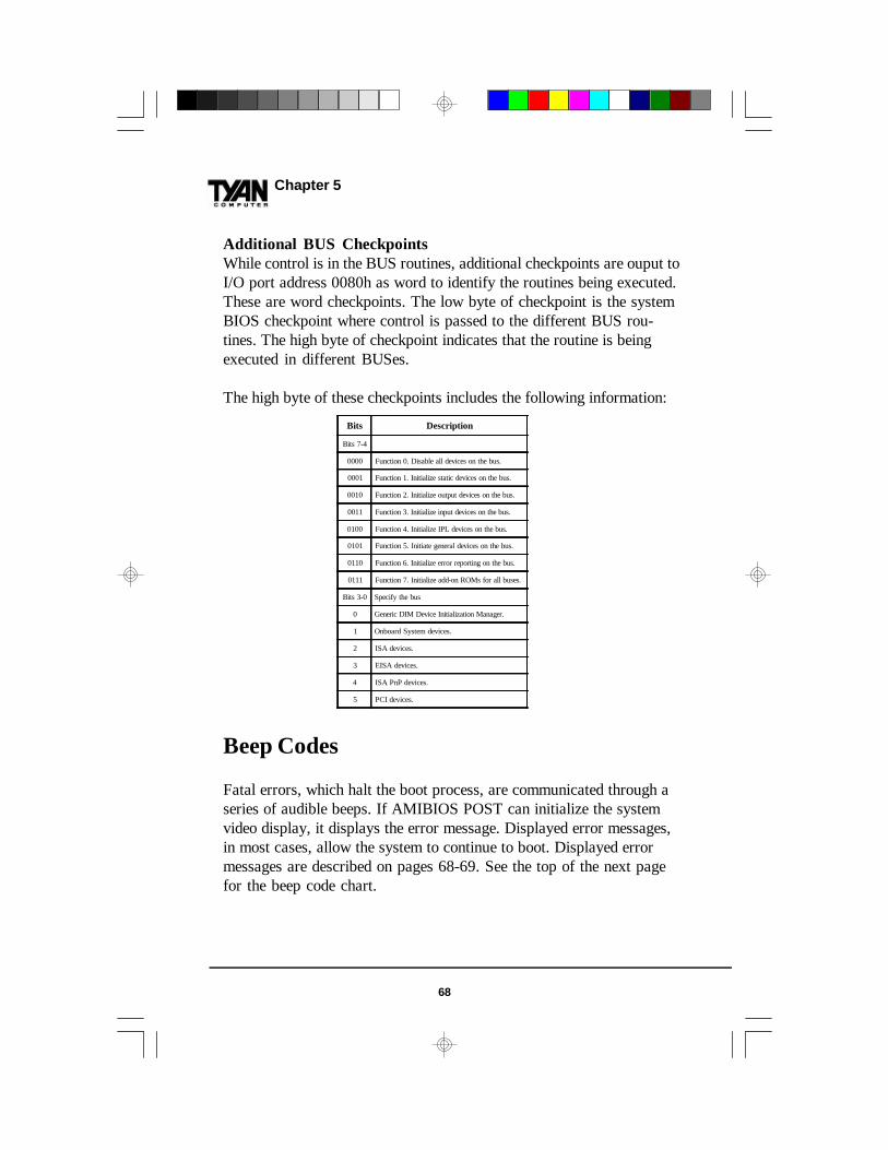
68
Chapter 5
Additional BUS CheckpointsWhile control is in the BUS routines, additional checkpoints are ouput toI/O port address 0080h as word to identify the routines being executed.These are word checkpoints. The low byte of checkpoint is the systemBIOS checkpoint where control is passed to the different BUS rou-tines. The high byte of checkpoint indicates that the routine is beingexecuted in different BUSes.
The high byte of these checkpoints includes the following information:
Beep Codes
Fatal errors, which halt the boot process, are communicated through aseries of audible beeps. If AMIBIOS POST can initialize the systemvideo display, it displays the error message. Displayed error messages,in most cases, allow the system to continue to boot. Displayed errormessages are described on pages 68-69. See the top of the next pagefor the beep code chart.
Bits Description
Bits 7-4
0000 Function 0. Disable all devices on the bus.
0001 Function 1. Initialize static devices on the bus.
0010 Function 2. Initialize output devices on the bus.
0011 Function 3. Initialize input devices on the bus.
0100 Function 4. Initialize IPL devices on the bus.
0101 Function 5. Initiate general devices on the bus.
0110 Function 6. Initialize error reporting on the bus.
0111 Function 7. Initialize add-on ROMs for all buses.
Bits 3-0 Specify the bus
0 Generic DIM Device Initialization Manager.
1 Onboard System devices.
2 ISA devices.
3 EISA devices.
4 ISA PnP devices.
5 PCI devices.

69
Troubleshooting System Problems
If the computer beeps... then...1, 2, or 3 times... reseat the memory SIMMs or DIPs. If
the system still beeps, replace thememory.
6 times... reseat the keyboard controller chip. Ifit still beeps, replace the keyboardcontroller. If it still beeps, try adifferent keyboard, or replace thekeyboard fuse, if there is one.
8 times... there is a memory error on the videoadapter. Replace the video adapter, orthe RAM on the video adapter.
9 times... the BIOS ROM chip is bad. Thesystem probably needs a new BIOSROM chip.
11 times... reseat the cache memory on themotherboard. If it still beeps, replacethe cache memory.
4, 5, 7, or 10 times... the motherboard must be replaced.
Beeps Error Message Description
1 Refresh Failure The memory refresh circuitry is faulty.
2 Parity Error Parity error in the base memory (the first 64 KB block) of memory.
3 Base 64 KB Memory Failure Memory failure in first 64 KB.
4 Timer Not Operational A memory failure in the first 64 KB of memory, or Timer 1 is notfunctioning.
5 Processor Error The CPU generated an error.
6 8042 - Gate A20 Failure Cannot switch to protected mode.
7 Processor Exception Interrupt Error The CPU on the CPU Card generated an exception interrupt.
8 Display Memory Read/Write Error The system video adapter is either missing or its memory is faulty. This isnot a fatal error.
9 ROM Checksum Error The ROM checksum value does not match the value encoded inAMIBIOS.
10 CMOS Shutdown Register Read/Write Error The shutdown register for CMOS RAM has failed.
11 Cache Memory Bad — Do Not Enable Cache The cache memory test failed. Cache memory is disabled. Do not press<Ctrl> <Alt> <Shift> <+> to enable cache memory.
SY
ST
EM

70
Chapter 5
Error Message Explanation
8042 Gate-A20 Error Gate A20 on the keyboard controller (8042) is not working. Replace the 8042.
Address Line Short! Error in the address decoding circuitry.
C: Drive Error No response from drive C:. Run the AMIDiag Hard Disk Utility. Check the C: harddisk type in Standard Setup.
C: Drive Failure No response from hard disk drive C:. Replace the drive.
Cache Memory Bad,Do Not Enable Cache! Cache memory is defective. Run AMIDiag.
CH-2 Timer Error An AT system has two timers. There is an error in timer 2.
CMOS Battery StateLow
CMOS RAM is powered by a battery. The battery power is low. Replace thebattery.
CMOS ChecksumFailure CMOS RAM checksum is different than the previous value. Run WINBIOS Setup.
CMOS SystemOptions Not Set The values stored in CMOS RAM have been destroyed. Run WINBIOS Setup.
CMOS Display TypeMismatch
The video type in CMOS RAM does not match the type detected. Run WINBIOSSetup.
CMOS Memory SizeMismatch
The amount of memory found by AMIBIOS is different than the amount in CMOSRAM. Run WINBIOS Setup.
CMOS Time and DateNot Set Run Standard Setup to set the date and time.
D: Drive Error No response from drive D:. Run the AMIDiag Hard Disk Utility. Check the harddisk type in Standard Setup.
Displayed Error Messages
If an error occurs after the system display has been initialized, the errormessage will be displayed as follows:
ERROR Message Line 1ERROR Message Line 2Press <F1> to continue
and the system halts. The system does not halt if Wait for <F1> If AnyError in Advanced Setup is Disabled.
RUN SETUP UTILITY
may also appear. Press <F1> to run WINBIOS Setup if this messageappears.

71
Error Message Explanation
D: drive failure No response from hard disk drive D:. Replace the drive.
Diskette Boot Failure The boot diskette in drive A: cannot be used to boot the system. Useanother boot diskette and follow the screen instructions.
Display Switch NotProper
Some systems require a video switch be set to either color ormonochrome. Turn the system off, set the switch properly, then power on.
DMA Error Error in the DMA controller.
DMA 1 Error Error in the first DMA channel.
DMA 2 Error Error in the second DMA channel.
FDD Controller Failure AMIBIOS cannot communicate with the floppy disk drive controller.Check all appropriate connections after the system is powered down.
HDD Controller Failure AMIBIOS cannot communicate with the hard disk drive controller. Checkall appropriate connections after the system is powered down.
INTR1 Error Interrupt channel 1 failed POST.
INTR2 Error Interrupt channel 2 failed POST.
Invalid Boot Diskette AMIBIOS can read the diskette in floppy drive A:, but it cannot boot thesystem with it. Use another boot diskette and follow the screen instructions.
Keyboard IsLocked...Unlock It
The keyboard lock on the system is engaged. The system must beunlocked to continue to boot.
Keyboard ErrorThe keyboard has a timing problem. Make sure a Keyboard ControllerAMIBIOS is installed. Set Keyboard in Advanced Setup to Not Installedto skip the keyboard POST routines.
KB/Interface Error There is an error in the keyboard connector.
No ROM BASIC Cannot find a proper bootable sector on either drive A: or C:. AMIBIOScannot find ROM Basic.
Off Board Parity Error
Parity error in memory installed on an adapter card in an expansion slot.The format is:
OFF BOARD PARITY ERROR ADDR = (XXXX)XXXX is the hex address where the error occurred. Run AMIDiag to find andcorrect memory problems.
On Board Parity Error
Parity error in motherboard memory. The format is:ON BOARD PARITY ERROR ADDR = (XXXX)
XXXX is the hex address where the error occurred. Run AMIDiag to findand correct memory problems.
Parity Error ???? Parity error in system memory at an unknown address. Run AMIDiag tofind and correct memory problems.
SY
ST
EM

72
Additional Manuals
Your motherboard package also contains the following three User’sGuides, in the Appendices section:A) Yamaha OPL3/OPL4 User’s GuideB) Adaptec SCSI 7800 Family Manager Set User’s GuideC) Adaptec AHA-3940AU/3940AUW User’s Guide
Note that the Adaptec AHA-3940AU/3940AUW User’s Guide con-tains instructions on installing the SCSI host adapter. As you havepurchased a TYAN motherboard with the SCSI chip onboard, you donot need to worry about installing the host adapter. Skip these sections.
Attention: You cannot install the SCSI driver for Windows NT 4.0 ifyou boot up directly from the CDROM. You must install Windows NT4.0 from the three diskettes provided by Microsoft.
Chapter 5
!