
Nonlinear Optics of Split-Ring Resonators and their ...
114
Nonlinear Optics of Split-Ring Resonators and their Application as a Thermal Detector Zur Erlangung des akademischen Grades eines DOKTORS DER NATURWISSENSCHAFTEN der Fakult¨ at f¨ ur Physik des Karlsruher Instituts f¨ ur Technologie (KIT) genehmigte Dissertation von Dipl.-Phys. Fabian Bernd Peter Niesler aus Pforzheim Tag der m¨ undlichen Pr¨ ufung: 19. Oktober 2012 Referent: Prof. Dr. Martin Wegener Korreferent: Prof. Dr. Kurt Busch
Transcript of Nonlinear Optics of Split-Ring Resonators and their ...

Nonlinear Optics of Split-Ring
Resonators and their Application
as a Thermal Detector
Zur Erlangung des akademischen Grades eines
DOKTORS DER NATURWISSENSCHAFTEN
der Fakultat fur Physik des
Karlsruher Instituts fur Technologie (KIT)
genehmigte
Dissertation
von
Dipl.-Phys. Fabian Bernd Peter Niesler
aus Pforzheim
Tag der mundlichen Prufung: 19. Oktober 2012
Referent: Prof. Dr. Martin Wegener
Korreferent: Prof. Dr. Kurt Busch

ii

Contents
1 Introduction 1
2 Basics of Optics 5
2.1 From Maxwell’s Equations ... . . . . . . . . . . . . . . . . . . . . 5
2.2 ... to Light Propagation . . . . . . . . . . . . . . . . . . . . . . . 7
2.3 Metal Optics . . . . . . . . . . . . . . . . . . . . . . . . . . . . . 9
2.3.1 The Drude Free-Electron Model . . . . . . . . . . . . . . . 9
2.4 Optics of Dielectrica . . . . . . . . . . . . . . . . . . . . . . . . . 11
2.5 Optics of Small Metal Particles . . . . . . . . . . . . . . . . . . . 12
2.6 Nonlinear Optics . . . . . . . . . . . . . . . . . . . . . . . . . . . 15
2.6.1 Symmetry Properties . . . . . . . . . . . . . . . . . . . . . 16
2.6.2 Nonlinear Optics of Dielectrics - The Anharmonic-Oscillator
Model . . . . . . . . . . . . . . . . . . . . . . . . . . . . . 18
2.6.3 Nonlinear Optics of Metals . . . . . . . . . . . . . . . . . . 21
2.6.3.1 The Nonlinear Drude Model . . . . . . . . . . . . 22
2.7 Optical Metamaterials . . . . . . . . . . . . . . . . . . . . . . . . 24
2.7.1 The Split-Ring Resonator . . . . . . . . . . . . . . . . . . 24
2.7.1.1 Excitation Configurations . . . . . . . . . . . . . 26
2.7.1.2 Higher-Order Resonances . . . . . . . . . . . . . 27
3 Materials and Methods 29
3.1 Sample Fabrication . . . . . . . . . . . . . . . . . . . . . . . . . . 29
3.2 Sample Characterization . . . . . . . . . . . . . . . . . . . . . . . 33
3.2.1 Linear Optical Characterization . . . . . . . . . . . . . . . 33
i

CONTENTS
4 Nonlinear Optical Experiments 35
4.1 SHG from Split-Ring Resonators on GaAs Substrate . . . . . . . 36
4.1.1 Nonlinear Optical Characterization . . . . . . . . . . . . . 38
4.1.2 Experimental Results and Discussion . . . . . . . . . . . . 41
4.1.3 Conclusions . . . . . . . . . . . . . . . . . . . . . . . . . . 45
4.2 SHG Spectroscopy on Split-Ring-Resonator Arrays . . . . . . . . 46
4.2.1 Sample Fabrication and Linear Optical Characterization . 46
4.2.2 Nonlinear Optical Characterization . . . . . . . . . . . . . 47
4.2.3 Experimental Results and Discussion . . . . . . . . . . . . 50
4.2.4 Conclusions . . . . . . . . . . . . . . . . . . . . . . . . . . 54
4.3 Collective Effects in Second-Harmonic Generation from Split-Ring-
Resonator Arrays . . . . . . . . . . . . . . . . . . . . . . . . . . . 55
4.3.1 Sample Fabrication and Linear Optical Characterization . 55
4.3.2 Experimental Results and Discussion . . . . . . . . . . . . 56
4.3.3 Conclusions . . . . . . . . . . . . . . . . . . . . . . . . . . 64
5 Thermal Detectors 65
5.1 Thermal Model . . . . . . . . . . . . . . . . . . . . . . . . . . . . 67
5.1.1 Heat Exchange Mechanisms . . . . . . . . . . . . . . . . . 68
5.1.2 Thermal Capacity . . . . . . . . . . . . . . . . . . . . . . . 71
6 Metamaterial Metal Bolometer 73
6.1 Basics of Metal Bolometers . . . . . . . . . . . . . . . . . . . . . . 74
6.2 Thermal Characterization of the Bolometer . . . . . . . . . . . . . 76
6.3 Experimental Setup . . . . . . . . . . . . . . . . . . . . . . . . . . 79
6.4 Experimental Results . . . . . . . . . . . . . . . . . . . . . . . . . 83
6.4.1 Conclusions . . . . . . . . . . . . . . . . . . . . . . . . . . 89
7 Conclusions and Outlook 91
References 95
ii

Publications
Parts of this work have already been published...
...in peer reviewed scientific journals:
• F.B.P. Niesler, N. Feth, S. Linden, J. Niegemann, J. Gieseler,
K. Busch, and M. Wegener,“Second-harmonic generation from
split-ring resonators on a GaAs substrate,” Opt. Lett. 34, 1997
(2009).
• F.B.P. Niesler, N. Feth, S. Linden, and M. Wegener, “Second-
harmonic optical spectroscopy on split-ring-resonator arrays,”
Opt. Lett. 36, 1533 (2011).
• F.B.P. Niesler, J.K. Gansel, S. Fischbach, and M. Wegener, “Meta-
material metal-based bolometers,” Appl. Phys. Lett. 100,
203508 (2012).
• S. Linden, F.B.P. Niesler, J. Forstner, Y. Grynko, T. Meier,
and M. Wegener, “Collective Effects in Second-Harmonic Gen-
eration from Split-Ring-Resonator Arrays,” Phys. Rev. Lett.
109, 015502 (2012).
...at scientific conferences (only own presentations):
• F.B.P. Niesler, S. Linden, N. Feth, and M. Wegener, “Second-
harmonic spectroscopy on split-ring-resonator arrays,” in “Con-
ference on Lasers and Electro-Optics / Quantum Electronics and
Laser Science Conference (San Jose, USA),” talk QTuA (2009).
• F.B.P. Niesler and M. Wegener, “Metamaterial bolometers,” in
“Conference on Lasers and Electro-Optics / Quantum Electron-
ics and Laser Science Conference (San Jose, USA),” talk QM3F
(2012).

• F.B.P. Niesler, S. Linden, J. Forstner, Y. Grynko, T. Maier, and
M. Wegener, “Collective effects in second-harmonic generation
from split-ring-resonator arrays,” in “Conference on Lasers and
Electro-Optics / Quantum Electronics and Laser Science Con-
ference (San Jose, USA),” talk QTh3E (2012).
Additional work on other topics has been published in peer
reviewed scientific journals:
• N. Feth, S. Linden, M.W. Klein, M. Decker, F.B.P. Niesler, Y.
Zeng, W. Hoyer, J. Liu, S.W. Koch, J.V. Moloney, and M. We-
gener, “Second-harmonic generation from complementary split-
ring resonators,” Opt. Lett. 33, 1975 (2008).

1
Introduction
A precise control of light propagation is one of the main driving forces of research
in the field of optics. The performance of optical elements for the alteration of
light propagation is determined by the optical properties of the materials avail-
able. However, all natural existing optical materials are limited to only control
the electric-field component of the light. The development of metamaterials in
recent years made a new material class available that allows the control of the
electric- as well as the magnetic-field component of the light independently. This
new degree of freedom allows in principle the design of novel and unprecedented
optical devices.
Metamaterials are artificial composite materials constructed from fundamen-
tal buildings blocks. These blocks are arranged in a lattice with a period smaller
than the corresponding wavelength of light that they were synthesized for. The
optical properties of the material are given by the geometrical shape of the blocks
and the materials used, often a combination of metals and dielectrics. Its optical
behavior can well be described by effective material parameters such as an electric
permittivity ε and a magnetic permeability µ.
The theoretical framework for this material class was founded by Veselago in
1968 [1] who studied the qualities of a, at that time purely fictitious, material
which exhibits a negative magnetic- and electric response ε, µ < 0. He discovered
dramatically different propagation characteristics of light within this material
such as a negative index of refraction. These novel optical phenomena sparked
further research. In 2000, the concept of a perfect lens was proposed by Pendry
[2] as a possible application for a negative refractive index material.
1

1. INTRODUCTION
On the way to a practical realization of such a material, a design of the
fundamental building block providing a magnetic response had to be found. In
1999, Pendry et al. [3] came up with the split-ring resonator (SRR). The basic
design consists of a metal ring with a small gap. Light impinging on this structure
induces an oscillating ring current which generates an oscillating magnetic dipole
moment. A negative index of refraction for a periodic arrangement of single
SRRs was demonstrated in 2001 by Shelby et al. [4] in the microwave region.
In later years, this concept was then brought to the optical domain through a
miniaturization of the SRRs down to dimensions on the nanometer scale using
advanced nano-fabrication techniques [5, 6].
Metamaterials are also the foundation for transformation optics [7]. By spa-
tially varying the effective material parameters ε, µ within the material, the flow
of light can be controlled. It can even be bent around objects to render them
invisible. The idea of the electromagnetic cloak goes back to work of Pendry et al.
[8] and Leonhard [9]. Through a vast improvement of 3D fabrication techniques,
this concept could be experimentally demonstrated at optical wavelengths only
recently [10].
Current research in the field of metamaterials is characterized by the search
for applications [11]. For example, perfect absorbers, neither transmitting of re-
flecting light in a certain wavelength range, have been demonstrated [12]. This
concept was then adapted for sensing and detection applications [13, 14]. Ther-
mal emitters, which provide a tailored emission spectrum [15, 16] also build up
on this idea. An investigation of the nonlinear optical properties of metamate-
rial structures is of scientific as well as technological interest. The research in
this area is motivated by the idea of developing efficient frequency converters or
optical switches using metamaterials, which outperform todays state-of-the-art
technologies. To reach this ambitious goal, a deeper understanding of the under-
lying physics is needed which can only be achieved through a sufficient amount
of experimental data, providing a test-ground for theory.
The experiments presented in this thesis aim to provide a contribution to
the progress in the field of linear and nonlinear optics of metamaterials and their
applications. The nonlinear optical experiments are focussed on second-harmonic
generation of gold split-ring resonator arrays as a paradigmatic building block of
2

metamaterials . Second-harmonic optical spectroscopy on these arrays, using a
sophisticated optical setup with a tunable light source, provides a deeper insight
on the role of the different resonances of the SRR as well as the spacing between
individual SRR on the generation of frequency doubled light.
In addition, this thesis presents a thermal detector based on a modified split-
ring resonator structure. This metamaterial metal-based bolometer is fabricated
and fully experimentally characterized. The proof of concept adds up to the list
of possible applications using metamaterials.
Outline of this Thesis
The first part of this thesis deals with experiments on second-harmonic generation
from split-ring resonator arrays. In the second part, the experimental demonstra-
tion of a metamaterial metal-based bolometer is presented.
In chapter 2, the thesis starts with a presentation of the basics of linear and
nonlinear optics. These are provided to the reader for a deeper understanding of
the experimental results in the later chapters. In addition, the working-horse of
this thesis, the split-ring resonator is elucidated.
Chapter 3 discusses the methods used for the fabrication and the linear optical
characterization of all samples in this thesis.
The experimental details and results for the nonlinear optical experiments on
SRR arrays are presented in chapter 4. In the first part, we study the interac-
tion of an SRR array with a substrate possessing a strong optical second-order
nonlinearity and compare the results with a theoretical modeling. In the second
part, second-harmonic-generation spectroscopy on gold SRR arrays fabricated on
glass substrates is presented. A tunable light-source in combination with litho-
graphic tuning of the individual SRR within the arrays was used to provide a
deeper insight onto the role of the individual resonances on the second-harmonic
generation. The third part finally studies the role of the spacing between indi-
vidual SRRs within an array on the second-harmonic generation intensity. The
experimental result is compared to numerical calculations.
In chapter 5, the basic working principles of thermal detectors are illus-
trated to provide the basis for the later presentation of the metamaterial metal-
bolometer concept in chapter 6. A full experimental characterization of the fabri-
cated bolometer is presented and compared to numerical calculations. This work
3

1. INTRODUCTION
is intended to provide a proof of concept of a thermal detector with build-in
spectral and polarization filters.
The thesis is finally concluded in chapter 7.
4

2
Basics of Optics
In this chapter, the basics of linear and nonlinear optics are treated. We start by
introducing the Maxwell equations for a basic description of light-matter inter-
action. Then, the models for the linear optical response of metals and dielectrics
are presented. In a next step, an introduction to nonlinear optics and the nonlin-
ear optical response of metals and dielectrics is presented. Finally, the split-ring
resonator and its optical properties are introduced.
2.1 From Maxwell’s Equations ...
To start our journey into the interaction of light with matter, we begin with the
set of macroscopic maxwell equations describing electromagnetic phenomena in
general. They read
∇ ·D = ρext, (2.1)
∇ ·B = 0, (2.2)
∇× E = −∂B
∂t, (2.3)
∇×H = jext +∂D
∂t, (2.4)
with the macroscopic fields D (the dielectric displacement), E (the electric field),
H (the magnetic field) and B (the magnetic induction), the external charge den-
sity ρext and the current density jext.
When the electric and magnetic fields E, H act on materials, they can induce
or reorient electric and magnetic dipoles. The polarization P describes the electric
5

2. BASICS OF OPTICS
dipole moment per unit volume inside the material, while the magnetization M
depicts the magnetic moment per unit volume. The constitutive relations account
for the presence of materials and have the form
D = ε0E + P, (2.5)
H =1
µ0
B−M, (2.6)
with the electric permittivity ε0 and magnetic permeability µ0 of the vacuum.
In the following, we consider a linear response of the materials, and the fields
P, M are connected with the corresponding response functions through
P(r, t) =
∫ε0χe(r− r′, t− t′)E(r′, t′)dt′d3r′, (2.7)
M(r, t) =
∫µ0χm(r− r′, t− t′)H(r′, t′)dt′d3r′. (2.8)
Here, r denotes the spatial coordinate, and the electric and magnetic susceptibil-
ity, χe and χe respectively, represent second-rank tensors.
The above general form of the susceptibilities can be simplified if special
material properties are fulfilled. In isotropic media, the tensors reduce to scalar
quantities because the dipoles are oriented parallel or antiparallel to the applied
fields. Homogenous media with a spatially local response remove the tensors
dependence on the space coordinate. No explicit time dependence and causality
results in a simplified representation
P(r, t) = ε0
∫ t
−∞χe(t− t′)E(r, t′)dt′, (2.9)
M(r, t) = µ0
∫ t
−∞χm(t− t′)M(r, t′)dt′. (2.10)
We now do a Fourier transformation of the above equations to go from the time
domain to the frequency domain. Finally, the expressions
P(ω) = ε0χe(ω)E(ω), (2.11)
M(ω) = µ0χm(ω)H(ω), (2.12)
are obtained and the material equations 2.8 can be rewritten as
D = ε0(1 + χe(ω))E = ε0ε(ω)E, (2.13)
B = µ0(1 + χm(ω))H = µ0µ(ω)H, (2.14)
6

2.2 ... to Light Propagation
with the relative electric permittivity εr = ε(ω) and the relative permeability
µr = µ(ω), which describe the response of the material.
In usual textbooks, a magnetization of materials through electromagnetic
fields at optical frequencies is often neglected, as natural existing materials show
no magnetic response for wavelengths in the visible. The excitement about optical
metamaterials is the idea of engineering values for εr, µr to change the materials
response to light waves, leading to unusual optical phenomena.
2.2 ... to Light Propagation
So far we have only processed the foundation of the interaction of magnetic and
electric fields with matter. But light as an electromagnetic wave is still hidden in
Maxwell’s equations. To reveal the traveling wave as a solution to the Maxwell
equations, we can rewrite them in the form(∇2 − µ0ε0
d2
dt2µrεr
)E = 0, (2.15)(
∇2 − µ0ε0d2
dt2µrεr
)B = 0. (2.16)
By using the ansatz for a plane wave for the electric and the magnetic field
E(r, t) = E0ei(kr−ωt) + c.c., (2.17)
B(r, t) = B0ei(kr−ωt) + c.c., (2.18)
with c.c. denoting the complex conjugate, we get the dispersion relation
k · k = µ(ω)ε(ω)ω2µ0ε0 = n(ω)2ω2
c20
= n2(ω)k20, (2.19)
which connects the frequency ω of the wave with the wave vector k through the
vacuum speed of light c0 = 1/√µ0ε0 and the complex refractive index
n(ω) =√ε(ω)µ(ω). (2.20)
In most naturally occuring materials, the magnetic response at optical fre-
quencies can be neglected and setting µr = 1 is justified. The behavior of
the refractive index is therefoe solely determined by the complex permeability
ε(ω) = εRe(ω) + iεIm(ω) through
n(ω) =√ε(ω)Re + iε(ω)Im (2.21)
7

2. BASICS OF OPTICS
with
εRe = n2 − κ2 (2.22)
εIm = 2nκ (2.23)
n2 =εRe
2+
1
2
√ε2Re + ε2Im, (2.24)
κ =εIm2n
(2.25)
The propagation of light is obviously strongly affected by the refractive index,
as it directly influences the wavevector k. The wave vector for a plane wave
propagating in z-direction has the form
kz = ωc0nez =
ω
c0
(n+ iκ)ez (2.26)
where ez denotes the unit vector in z-direction. For the electrical field of a plane
wave 2.18 we then get
E(z, t) = E0 ·
propagation︷ ︸︸ ︷eiω(n(ω)z/c0−t) · e−(ωκ(ω)z/c0)︸ ︷︷ ︸
attenuation
. (2.27)
Here we see that the real part n(ω) of the refractive index determines the wave
propagation, while the imaginary part κ(ω) accounts for a attenuation of the wave
and is therefore called the extinction coefficient. It is linked to the absorption
coefficient α of Beer’s law,
I(z) = I0e−αz. (2.28)
It describes the exponential decay of the intensity I(z) of a beam propagation
through an absorbing medium along the z-direction. This can be easily seen by
using I(z, t) ∝ |E(z, t)|2 on 2.27 and comparing the result with 2.28. We obtain
α(ω) =2ωκ(ω)
c0
. (2.29)
One can define a characteristic length scale on which the intensity of the wave
dropped to a value of 1/e of its initial intensity. This so called skin depth is given
by δz = 1/α(ω).
8

2.3 Metal Optics
2.3 Metal Optics
To describe the optical response of metals, we introduce the Drude free-electron
model. We will see that the dielectric function of this model is strongly linked to
the electrical conductivity of the metal.
2.3.1 The Drude Free-Electron Model
The model of free electrons is a classical model described in principle by Drude
in 1900. Within this model he was able not only to explain the conduction of
both, electricity and heat, but also the optical properties of metals. It is based
on the following assumptions. First of all, the metal consist of electrons that
can move freely. The movement of these conduction electrons is disturbed by
instantaneous and uncorelated collision processes with ions and impurities within
the metal. The probability of such a collision during a time interval dt is given
by dt/τ , where τ describes the relaxation time. An electron-electron interaction
process is neglected at all in this model.
The equation of motion for one electron with the mass me is given by
med2
dt2r +
me
τ
d
dtr = −eE(t), (2.30)
where the electric field acts as a driving force. Now we apply a harmonic time
dependent field E(t) = E0e−iωt which leads to the solution for the displacement
of the electron
r(t) =e
m(ω2 + iγω)E(t), (2.31)
with γ = 1/τ denoting the collision frequency and r(t) = x0e−iωt.
The macroscopic polarization P is then given as a product of n electrons in
the unit volume:
P = −ner = − ne2
m(ω2 + iγω)E. (2.32)
The constitutive relation reads
D = ε0
(1−
ω2pl
ω2 + iγω
)E, (2.33)
9

2. BASICS OF OPTICS
with the plasma frequency ω2pl = ne2
ε0m. By comparing this with equation 2.13, we
have the dielectric function of the Drude free-electron gas given by
ε(ω) = 1−ω2
pl
ω2 + iγω. (2.34)
We now take a closer look on the current density. The electrical current I is
defined as
I = dQdt
(2.35)
where Q denotes the amount of charge. The charge density is defined as j = I/A
and we get
j = −nevd, (2.36)
with vd denoting the drift velocity of electrons. Writing the equation of motion
2.30 using the impulse p = mx, we have
p+p
τ= −eE0e
−iωt. (2.37)
Using the ansatz p = p0 · e−iωt, we obtain the solution
vd = x = −eτm
11−iωτE0. (2.38)
Now we insert this result in equation 2.36 to obtain
j = ne2τm
11−iωτE0 (2.39)
= σ01−iωτE0 (2.40)
= σ(ω)E0 (2.41)
which is Ohm’s law with the AC conductivity σ(ω) and DC conductivity σ(0) =
σ0. If we insert this into 2.34, we get
ε(ω) = 1 + iσ(ω)
ε0ω, (2.42)
where we see, that the metals dielectric function is linked to its frequency depen-
dent conductivity.
10

2.4 Optics of Dielectrica
2.4 Optics of Dielectrica
In dielectrica, the electrons are bound to the atomic cores and cannot move freely
like in metals. An applied static electric field leads to a deviation of the electrons
position from the rest position. The response is therefor different compared to
metals, where a static electric field leads to a drift velocity of the electrons. The
model of a damped harmonic oscillator (Lorentz oscillator), driven by an external
harmonic electric field, is
med2
dt2r +meΓ
d
dtr +meω
20r = −eE0e
−iωt, (2.43)
where Γ = 1/γ describes the damping of the electron’s movement. The damping
factor accounts for an energy loss of the electron due to radiation and electron-
phonon interaction. With the same reasoning as for the free-electron model in
metals, we get the electric dipole moment per unit volume through multiplying
all n electrons
P = −ner(t) =ne2
me
1
ω20 − ω2 − iΓω
E0e−iωt. (2.44)
We get the same result with the plasma frequency ωpl
D = ε0
(1 +
ωpl
ω20 − ω2 − iωΓ
)E. (2.45)
Now that we have analytical expressions for the response of the material, we
will take a closer look on the influence on the propagation of light. We have seen,
that the absorption coefficient of the material depends on the imaginary part of
the dielectric function.
In figure 2.1 (a) the real and imaginary parts of the dielectric function for
metals, as obtained by the free electron model, are plotted. For frequencies below
the plasma frequency, ω << ωpl, the imaginary part of the dielectric function
leads to an absorption of the electromagnetic wave. In this regions, the light wave
is attenuated on the length-scale of the skin depth. The absorption coefficient
2.29 is
α(ω) =
√2ω2
plτω
c0
. (2.46)
11

2. BASICS OF OPTICS
Figure 2.1: Dielectric functions in the Drude and Lorentz model - Both
plots show the real (blue line) and imaginary (red line) part of the dielectric func-
tion. In (a), permittivity for metals, as obtained from the free electron model, is
depicted. In (b), a dielectrica described with the damped oscillator model is pre-
sented. For both figures, a plasma frequency of ωpl = 1 and a damping constant of
γ = 0.1 is chosen. The resonance frequency in (b) is ω0 = 0.5.
For frequencies above the plasma frequency ω >> ωpl, the real part of the dielec-
tric function dominates. Here, a wave propagation through the metal is possible
and they become transparent.
With the same reasoning, dielectrics in figure 2.1 (b) show the same behavior
for frequencies above and below the resonance frequency ω >> ω0 and ω >> ω0.
In this region, they are transparent to light waves. But near the resonance ω ≈ ω0,
the dominant imaginary part of the dielectric function leads to a strong absorption
of waves.
2.5 Optics of Small Metal Particles
In the previous chapters, we have modeled the reaction of electrons in bulk matter
to an external electric field. When bulk metals are drastically reduced in size and
reach dimensions smaller than the wavelength of light, their optical response can
no longer be described by the Drude free-electron model. In this case the elec-
tromagnetic wave has a constant spatial phase along the particle and the electric
field can be assumed as static (quasi-static approximation). The electromagnetic
12

2.5 Optics of Small Metal Particles
wave shifts the electrons inside the particle relative to the fixed positive ions of
the lattice. This leads to a charge separation resulting in a restoring force acting
on the deviated electrons. The equation of motion for the electrons is now given
by a driven harmonic oscillator, as described before with the Lorentz oscillator
model. An external field in resonance with the eigenfrequency of the particle then
leads to a collective electron oscillation, called particle plasmon.
Figure 2.2: Particle plasmon - Illustration of a particle plasmon excited by an
sinusoidal oscillating external electric field with the period T .
Within the quasi static approximation, analytical expressions for spherical
and elliptical particles can be found. For a metal sphere, the polarizability α(ω)
describing the electric dipole moment of the particle p = ε0εmαE, is given by [17]
α(ω) = 4πa3 ε(ω)− εsε(ω) + 2εs
, (2.47)
where a denotes the radius of the sphere. ε(ω) is the metals dielectric function and
εs describes the dielectric constant of the surrounding material. The resonance
condition is fulfilled when the denominator |ε+2εs| is minimized. For a vanishing
imaginary part of the dielectric constant =[ε], this corresponds to the Frolich
condition:
<[ε(ω)] = −2εs. (2.48)
When we now use the dielectric function as obtained from the Drude model, we
can deduce the resonance condition for a metal sphere as
ω0 =ωpl√
−(2εs + 1). (2.49)
13

2. BASICS OF OPTICS
Here we see that the resonance position strongly depends on the plasma frequency
ωpl of the metal and the dielectric constant εs of the surrounding material but is
does not depend from the size of the nano-sphere. This makes metal nanoparticles
an ideal tool for sensing applications, as any change of the surrounding dielectric
leads to an altered resonance frequency of the particle that can be monitored
optically [18].
For elliptical particles, the polarizability becomes a tensor accounting for the
different geometry of the particle. The expressions for the polarizability along
the particle’s principal axes i ∈ 1, 2, 3 is given by [17, 19]
αi = Vε(ω)− εm
εm + Fi(ε(ω)− εm), (2.50)
with V representing the volume of the ellipsoid. Here the Frolich condition does
give a size dependent resonance frequency of the particle due to the geometry
factor Fi.
If the particle size no longer satisfies the quasi static approximation, an ana-
lytical solution can still be found in the special case of spherical particles. The
so-called Mie theory is a more general expression for the optical properties of
metal nanoparticles [19, 20], but will not be discussed in greater detail here. For
arbitrarily shaped particles, numerical modeling of the optical properties has be
used.
Another inherent feature connected with the plasmonic resonances of metal
nanoparticles is the enhancement of the near field around the particle. The
intensity of the local field Iloc = |Eloc| compared to the incoming field I0 = |E0|differs by the frequency dependent enhancement factor L(ω) [17]
Iloc = L(ω) · I0 = L(ω)SPLLRI0. (2.51)
Two physical effects a responsible for the field enhancement. The so called light-
ning rod effect is responsible for the frequency independent contribution LLR and
is strongly depending on the geometrical shape of the particle. The electric field
on the surface of a perfect conductor points perpendicular to the surfaces nor-
mal, therefor leading to a concentration of the electromagnetic field to areas of
sharp edges or tips. The frequency dependent part L(ω)SP is due to the resonant
14

2.6 Nonlinear Optics
excitation of localized surface plasmons in the structure and essentially resembles
the polarizability α. For a spherical particle in vacuum this reads
L(ω)SP ∝ε(ω)− 1
ε(ω) + 2.. (2.52)
The frequency dependent enhancement can also be expressed by the quality factor
of the damped linear oscillator with the resonance frequency ω0
Q =ω0
γ, (2.53)
where γ describes the damping of the oscillator. The quality factor is also known
as the resonant amplification factor of the oscillator and describes the enhance-
ment of the oscillation amplitude of a driven oscillator system with respect to the
driving amplitude. This corresponds to the local-field enhancement in the case
of a particle plasmon.
2.6 Nonlinear Optics
The wave theory of light is based on the superposition principle. Light beams
which travel in a linear medium can pass through one another without disturbing
each other. However, in nonlinear media things are a bit different rendering
Huygen’s principle of superposition invalid.
The description of the material’s response to electromagnetic fields in the
former chapters is only valid in the case of low field intensities. In the presence of
very strong optical fields, the dielectric polarization now responds nonlinearly to
the electric field of light. This leads to an interaction of optical fields mediated
by the material. In contrast to linear optics, the fields are now no longer linearly
superimposable. With the invention of the laser, making strong electrical fields
experimentally accessible, theses effects became observable in the lab [21].
To describe this behavior theoretically, we can expand the dielectric polariza-
tion density as a Taylor series in the electric field
P(ω) = ε0χ(1)(ω, ω1) E(ω1) (2.54)
+ε0χ(2)(ω, ω1, ω2) E(ω1)E(ω2) (2.55)
+ε0χ(3)(ω, ω1, ω2, ω3)) E(ω1)E(ω2)E(ω3) (2.56)
+ . . . , (2.57)
15

2. BASICS OF OPTICS
where the χ(i), i > 1 denote the nonlinear optical susceptibilities of i-th order and
represent tensors of rank i+ 1.
Splitting of the polarization in its linear and nonlinear parts
P(ω) = Plinear(ω) + Pnonlinear(ω) (2.58)
then leads to a wave equation representation in the frequency domain [22]
∇2E(ω) +ω2ε(ω)
c2E(ω) =
ω2
c2Pnonlinear(ω). (2.59)
The nonlinear polarization on the right hand side of this inhomogenous wave
equation acts as a driving force.
2.6.1 Symmetry Properties
We will take a closer look on the symmetry properties of the χ(2) tensor, but
similar arguments can be found for the tensors of higher orders. In the most
general case for the nonlinear polarization of second order,
P(2)i (ωn + ωm) = ε0
∑jk
∑(nm)
χ(2)ijk(ωn + ωm, ωn, ωm)Ej(ωn)Ek(ωm), (2.60)
the nonlinear susceptibility consists of 324 different complex numbers, that need
to be defined. Fortunately, by using symmetry arguments, this number can be
greatly reduced.
The fact that the polarization as well as the electric fields represent physical
measurable quantities and therefore must be real, results in
P(2)i (−ωn − ωm) = Pi(ωn + ωm)∗, (2.61)
Ej(−ωn) = Ej(ωn)∗, (2.62)
Ek(−ωm) = Ek(ωm)∗, (2.63)
that leads to equal tensor components
χ(2)ijk(−ωn − ωm,−ωn,−ωm) = χ
(2)ijk(ωn + ωm, ωn, ωm)∗. (2.64)
In addition, the order of the fields on the right hand side of 2.60 is arbitrary. This
intrinsic permutation symmetry gives
χ(2)ijk(ωn + ωm, ωn, ωm) = χ
(2)ikj(ωn + ωm, ωm, ωn). (2.65)
16

2.6 Nonlinear Optics
When the material can be considered lossless, two more symmetries can be ap-
plied. We then can require the nonlinear susceptibility to be real which expresses
as
χ(2)ijk(ωn + ωm, ωn, ωm) = χ
(2)ijk(ωn + ωm, ωn, ωm), (2.66)
and the full permutation symmetry leads then to a free interchange of the fre-
quency arguments as long as the corresponding spatial coordinates are inter-
changed as well:
χ(2)jik(ωn + ωm, ωn, ωm) = χ
(2)kij(ωm, ωn + ωm,−ωn). (2.67)
In case of a neglectable frequency dispersion of χ(2) we can even permute the spa-
tial indices and frequency arguments independently, which is called the Kleinman
symmetry.
Figure 2.3: Euler Angles - Illustration
of the Euler angles to get from an initial
coordinate system xyz (black arrows) to a
rotated system XYZ (red arrows).
The occurrence of nonlinear optical
effects strongly depends on the sym-
metry class of the material, because
the crystal symmetry also influences
the symmetry of its physical proper-
ties. This fact is known as the Neu-
mann’s principle. It states, that a ten-
sor, which represents a physical prop-
erty, is invariant under symmetry oper-
ations which leave the crystal itself in-
variant [23]. Spatial symmetry there-
fore can further reduce the number of
independent tensor elements.
The transformation behavior for
the components mlmn of a tensors of
rank three is
m′ijk =∑l
∑m
∑n
AilAjmAknmlmn, (2.68)
where A denotes the transformation matrix. We now apply this rule to the χ(2)
tensor of an inversion symmetric medium. In this case, the symmetry operation is
17

2. BASICS OF OPTICS
given by the transformation matrix with the only nonzero elements A11 = A22 =
A33 = −1. This results in vanishing tensor components, (χ(2)ijk)′ = −χ(2)
ijk = 0.
Therefore, nonlinear optical effects of second order, or more general of even order,
are not found in inversion symmetric media.
When the crystal is rotated in the laboratory frame of reference, the transfor-
mation matrix can be obtained using the Euler angles which describe the crystals
rotation. The matrix is given by
A(α, β, γ) =
cosα sinα 0− sinα cosα 0
0 0 1
(2.69)
·
1 0 00 cos β − sin β0 sin β cos β
(2.70)
·
cos γ − sin γ 0sin γ cos γ 0
0 0 1
(2.71)
using the set of angles α, β, γ according to figure 2.3. This principle will be used
to interpret the experimental results in chapter 4.1.
2.6.2 Nonlinear Optics of Dielectrics - The Anharmonic-
Oscillator Model
We have already seen that the Lorentz model is adequate in describing the optical
properties of dielectric materials. Therefor it is obvious to extend this model to
describe the nonlinear response to find an expression for the nonlinear optical
susceptibility.
The equation of motion for the electron is described using a nonlinear restoring
force Fnonlinear caused by an anharmonic potential. The equation of motion can
then be written in a generic form
x+ 2γx− Frestoring = −eE(t)/m. (2.72)
To describe the potential mathematically, we use a taylor series expansion of the
restoring force with respect to the displacement x of the electron [22].
U(x) = −∫Frestoringdx =
1
2mω2
0x2 +
1
3max3 − 1
4mbx4 (2.73)
18

2.6 Nonlinear Optics
With this representation, we have restricted ourselves to displacements that are
small enough to not include higher terms in the series for a adequate description
of the potential and a > b.
The first term represents the harmonic potential and reproduces the restoring
force Frestoring = −mω20x
2 used in equation 2.43. The latter terms account for the
deviation of the potential from the perfect parabolic shape and are responsible
for the nonlinear restoring force.
To find the solutions to 2.72 we first have to consider the exact form of the
potential which depends on the symmetry of the medium. In case of centrosym-
metric media, it is required that U(x) = U(−x), therefore leading to a = 0 and
b 6= 0. The lowest nonlinear optical susceptibility in this case is of third order and
nonlinear susceptibilities of even order vanish. In contrast, non-centrosymmetric
media, described by U(x) = −U(−x), possess even and odd orders for the non-
linear optical susceptibility.
The equation of motion for non-centrosymmetric media is then
x+ γx+ ω20x+ ax2 = −eE(t)/m (2.74)
and the electric field, acting on the electron is assumed to be two plane waves of
different frequencies, described by
E(t) = E1e−iω1t + E2e
−iω2t + c.c. (2.75)
where c.c. denotes the complex conjugate. To solve the equation of motion 2.74
we use perturbation theory, known from quantum mechanics, where we replace
E(t) with λE(t), with 0 ≤ λ ≤ 1 as an expansion parameter. We now have
x+ γx+ ω20x+ ax2 = −λeE(t)/m (2.76)
and we will try to find solutions using the power series ansatz
x = λx(1) + λ2x(2) + λ3x(3) + . . . . (2.77)
Insertion and sorting by powers of the expansion parameter results in the equa-
tions
x(1) + γx(1) + ω20x
(1) = −eE(t)/m (2.78)
x(2) + γx(2) + ω20x
(2) + a(x(1))2 = 0 (2.79)
x(3) + γx(3) + ω20x
(2) + 2ax(1)x(2) = 0 (2.80).... (2.81)
19

2. BASICS OF OPTICS
The first equation reproduces the familiar solution from the Lorentz oscillator
x(1)(t) = x(1)(ω1)e−iω1t + x(1)(ω2)e−iω2t + c.c. (2.82)
with amplitudes
x(1)(ωj) = − e
m
EjD(ωj)
(2.83)
and the complex denominator function D(ωj) = ω20−ω2
j−iωjγ. Using the relation
P (1)(ωj) = ε0χ(1)(ωj)E(ωj) = −Nex(1)(ωj), (2.84)
we reproduce the linear susceptibility
χ(1)(ωj) =N(e2/m)
ε0D(ωj). (2.85)
To now solve the equation for the second order correction term x(2)(t), we have to
insert the equation for x(1)(t) into 2.79. This leads to an inhomogenous differential
equation, where the source term on the right hand side describes second-harmonic
generation (2ω1 and 2ω2), sum- (ω1 + ω2) and difference- (ω1 − ω2) frequency
generation as well as optical rectification for zero frequency.
For example, second-harmonic generation is described by the equation
x(2) + γx(2) + ω20x
(2) =−a(eE1/m)2e−2iω1t
D2(ω1)(2.86)
that can be solved by using the ansatz x(2)(t) = x(2)(2ω1)e−2iω1t. With this ansatz,
we obtain
x(2)(2ω1) =−a(e/m)2E2
1
D(2ω1)D2(ω1)(2.87)
which gives us an expression for the nonlinear susceptibility describing second-
harmonic generation by using
P (2)(2ω1) = ε0χ(2)(2ω1, ω1, ω1)E(ω1)2 = −Nex(2)(2ω1). (2.88)
We finally obtain
χ(2)(2ω1, ω1, ω1) =N(e3/m2)a
ε0D(2ω1)D2(ω1). (2.89)
So far, we have only considered the nonlinear effects of second order. From the
above equation, we again see that for an observation of these effects, a nonvanish-
ing a and therefore a non-centrosymmetric medium is required. Effects of third
order can be obtained in an analogous way by solving the equation for x(3) but
will not be presented here. The interested reader might consult reference [22].
20

2.6 Nonlinear Optics
2.6.3 Nonlinear Optics of Metals
Optical second-harmonic generation from a metal surface was first discovered in
1965 [24] and extensively studied experimentally in the years after. Early work on
the theoretical side was based on the free-electron model formulated by Jha [25].
Within this model, the nonlinear polarization varying at twice the fundamental
frequency ω has the form
P(2)NL = α(E1 ×H1)︸ ︷︷ ︸
bulk term
+ βE1∇ · E1︸ ︷︷ ︸surface term
(2.90)
where E1 and H1 represent the electric and magnetic fields at the fundamental
frequency and the coefficients α and β have been determined as [26]
α = ie3n4m2
eecω3 , (2.91)
β = e8πmeωplω2 , (2.92)
where me and e are the mass and the charge of an electron, and n is the electron
density. The plasma frequency is ωpl =√
4πne2/me. The first term is the
magnetic dipole term and represents a contribution from within the volume of
the metal originating from the Lorentz force. In contrast, the second term is the
magnetic quadrupole term and is nonzero only near the surface of the metal.
While this model could provide some estimates of the contributing mech-
anisms, its mathematical flaws and limitations have been discussed by several
authors [27, 28, 29, 30]. For example, the permittivity ε(ω) within this model is
given by [26]
ε(ω) = 1− e2n
mω2. (2.93)
This real and negative permittivity is not a valid description for real metals.
Because the permittivity depends on the electron density n, it shows a transition
from a negative value within the metal volume to a positive value ε(ω) = 1 in the
vacuum where the electron density is zero. In the transition region at the surface
the permittivity vanishes at the boundary. Here, the normal component of the
electric field tends to infinity due to the continuity relations. This is a clearly
unphysical behavior. Rudnick and Stern [29] also pointed out the need for a more
careful analysis of the metal-vacuum interface.
21
2. BASICS OF OPTICS
In the 1980s, a hydrodynamic model relevant for nonlinear optical effect in
metals was formulated by Sipe et al. [31]. Later, it was was slightly modified
by Schaich and Corvi [32]. The main idea of describing the electrons through
an electron density ne(r, t) and a velocity field ve(r, t) is also the basis for more
recent theories and numerical calculation schemes for the nonlinear response of
metals,metal particles, and metamaterial structures [33, 34, 35].
2.6.3.1 The Nonlinear Drude Model
The nonlinear Drude model, as described by Liu et al. [34], can be viewed as
a generalization of the linear Drude model to the nonlinear case. The electrons
within the metal are treated as a fluid, described by the electron density ne =
ne(r, t) and velocity ve(r, t)e. These quantities together with the fields E and B
are connected via the cold-plasma equations
∂ne∂t
+∇ · (neve) = 0, (2.94)
∂ve∂t
+ (ve · ∇)ve =qeme
(E + ve ×B), (2.95)
and the Maxwell equations
∇ ·B = 0 (2.96)
ε0∇ · E = ρ (2.97)
∂B
∂t= −∇× E (2.98)
ε0∂E
∂t= 1
µ0∇×B− j (2.99)
with the electron mass me, the electron charge qe, the permittivity ε0 and per-
meability µ0 of the vacuum. The charge density ρ and the current density j are
defined as
ρ = q(ne − n0), (2.100)
j = qeneve, (2.101)
with the positive ion density n0.
We can now rewrite the cold-plasma equations using the charge density 2.100
and current density 2.101. Equation 2.94 then reads
∂ρ
∂t= −∇ · j. (2.102)
22

2.6 Nonlinear Optics
The term on the left-hand side in equation 2.95 is the convective derivative
known from fluid mechanics. It is a derivative taken with respect to a moving
coordinate system and has the general form
D
Dt=
∂
∂t+ v · ∇, (2.103)
where v represents the velocity of the fluid. Applied to the current density j this
results in an identical represention of equation 2.95
∂j
∂t+∑k
∂
∂xk
jjkqene
=qeme
(qeneE + j×B)− 1
τj, (2.104)
where a phenomenological time constant τ was introduced to describe the current
decay due to Coulomb scattering.
The final set of equations, that has to be solved using a numerical scheme, is
then given by [33]
∂B
∂t= −∇× E (2.105)
∂E
∂t= 1
ε0µ0∇×B− 1
ε0j (2.106)
and
∂j
∂t= −1
τ+ ε0ω
2plE +
qeme
(ρE + j×B)−∑k
∂
∂xk
(jjk
ρ+ ε0meω2pl/qe
)(2.107)
where ωpl(r) =√q2en0(r)/(ε0me) denotes the space-dependent plasma frequency.
Equation 2.102 can be obtained by applying the divergence to the Maxwell equa-
tion 2.105. The charge density ρ can be viewed as a function of the electric field
since each occurrence of ρ can be replaced by
ρ = ε0∇ · E. (2.108)
We can see that the last two terms in equation 2.107 introduce the nonlinearity
to the system. The first two terms describe the linear Drude model as can be
seen by writing equation 2.37 in terms of the current density. This results in
∂j
∂t= −1
τj + ε0ω
2plE. (2.109)
23

2. BASICS OF OPTICS
2.7 Optical Metamaterials
We have seen, that the response of a material to light waves can be described
by using effective material parameters εr and µr which neglect microscopic inho-
mogenities . The effective medium description is valid, as long as the wavelength
of light is much larger than the microscopic structure of the material. But this
also makes it possible to synthesize materials with a tailored optical response by
engineering subwavelength building blocks and arrange them in a lattice with a
subwavelength period. The optical properties are therefore not solely determined
by the materials used for the blocks, but also by the shape of each block. This
material class is called photonic or optical metamaterials and is able to show
optical properties not found in natural existing materials.
On of the most prominent optical phenomena that can be implemented with
the photonic metamaterial concept is a negative index of refraction and was
already theoretical investigated by Vaselago in 1968 [1]. For a negative real part
of the index of refraction, the real parts of ε and µ both have to be negative as well
in the same spectral region. While the former is given for metals at their plasma
frequency the latter is not found in natural materials for optical frequencies.
Therefor, clever designs for a metamaterial fundamental building block have to
be invented to achieve a magnetic response at optical wavelengths. The invention
of the split ring resonator by Pendry [3] and the experimental proof of principle
by Smith et al. [36] served as a prototype for a magnetic building block.
2.7.1 The Split-Ring Resonator
We will now take a closer look on the design of a metamaterial building block
to achieve a magnetic dipole moment at optical frequencies, namely the split-
ring resonator (SRR). In essence, it is a simple U-shaped metal structure where
external electric and magnetic fields can induce an oscillating ring current within
the structure. This ring current then causes a magnetic dipole moment.
In that way, the SRR resembles the working principle of a LC-circuit, where
the wire represents on winding of a coil with the inductance L and the gap
between the wires forms a capacitor with the capacitance C (see figure 2.4 (b)).
The eigenfrequency of the circuit is given by
ωLC =1√LC
. (2.110)
24

2.7 Optical Metamaterials
Figure 2.4: SRR and LC-circuit analogy - The U-shaped metal structure
with its geometrical dimensions is depicted in (a) while (b) emphasizes the analogy
of the structure with a LC-circuit. A magnetic dipole moment m is connected with
the oscillating current j within the SRR (c).
To bring this frequency into the optical spectral region, the capacitance and
inductance therefore need to be very small. The eigenfrequency can be expressed
in terms of the dimensions of the SRR in figure 2.4 (a) by using the formula for
the capacitance of a plate capacitor
C = ε0εrplate area
plate distance= ε0ε
(ly − h)t
d, (2.111)
and the inductance of a coil having one winding
L = µ0coil area
coil length= µ0
lxlyt. (2.112)
This gives the eigenfrequency
ωLC =c0√εrlxly
√d
ly − h∝ 1
area, (2.113)
with c0 = 1/√ε0µ0 as the vacuum speed of light.
For the special case of an quadratic SRR with lx = ly = l and h = w = d we
can estimate the dimensions using equation 2.113. For a resonance frequency of
2π×200×1012 1/s which corresponds to a wavelength of λ0 = 2πc0/ω0 = 1.5 µm
we then obtain for εr = 1 the dimensions l = 150 nm and w =50 nm [37].
This result is interesting because we can see that the dimensions of the mag-
netic building blocks are clearly smaller than the wavelength of light that they
were designed for (λ0 = 1.5 µm). Therefor they can be arranged in a periodic
25

2. BASICS OF OPTICS
lattice with subwavelength lattice constants. That way, a medium with effective
optical parameters can be implemented, the basic idea of metamaterials. It is
also obvious that for a fabrication of such small metal structures sophisticated
nano-fabrication techniques are needed.
2.7.1.1 Excitation Configurations
In the last chapter, we have alluded that a magnetic resonance within a SRR
can be excited through external electric and magnetic fields. What exact field
component of the incoming light couples to the resonance of the SRR depends
on the excitation configuration, that is the orientation of the SRR relative to
the external fields. The incoming linear-polarized light wave is characterized
by its propagation direction and the polarization direction. With respect to the
propagation direction, which is determined through the wave vector k, three basic
configurations of the SRR relative to the wave vector can be distinguished. For
each of the three configurations, two additional arrangements of the polarization
direction can be differentiated.
Figure 2.5: Excitation configurations of a SRR - The three different excita-
tion configurations of the SRR relative to the wave vector k are shown. For each
configuration, only one polarization direction (as emphasized by the grey box) of
the incoming light can excite the magnetic resonance.
In figure 2.5 (a) the electric component of the incoming light couples to the
capacitor of the LC-circuit to excite the ring current while in configurations (b)
and (c) the magnetic component couples to the coil. For most experimental
studies of the magnetic resonance of SRR arrays, configuration (a) is choosen [6,
38] because the fabrication can be done rather easy using 2D pattern techniques
26

2.7 Optical Metamaterials
like electron-beam lithography or focussed ion beam milling [39]. Configuration
(b) has only recently been implemented for resonance frequencies in the THz
range [40]. Earlier studies used modified SRR designs such as cut-wire and plate
pairs [41]. This thesis will also focus on the most common excitation configuration
2.5 (a) of planar split-ring resonators arrays.
2.7.1.2 Higher-Order Resonances
We have seen that the LC-circuit model provides a simple description of the
magnetic resonance of a SRR . However, experimental and theoretical studies [6]
revealed the existence of additional resonances with higher frequencies than the
fundamental magnetic resonance rendering the LC-circuit model invalid for an
adequate description of those higher order excitations.
Figure 2.6: Eigenmodes of a straight antenna compared to an SRR -
The fundamental mode (a.1), first-order mode (a.2) and second-order mode (a.3)
of a straight antenna are depicted. For a direct comparison, the corresponding
eigenmodes (b.1), (b.2), (b.3) of a split-ring resonator are depicted. The red and
blue arrows indicate the polarization direction of the exciting plane wave and black
arrows represent the direction of the electric current.
To explain these resonances, we can model the SRR as a folded wire antenna.
Unfolding this U-shaped wire leaves us with a simple half wave antenna where
27

2. BASICS OF OPTICS
we know that a resonant excitation displays standing waves. The wavelength of
these standing waves it determined by the length l of the antenna:
λn = n · 2 · l. (2.114)
Here the integer n denotes the order of harmonics with n = 1 describing the
fundamental mode.
Within this fashion, figure 2.6 shows the antenna modes and their equivalent
plasmonic excitation in the SRR. The fundamental mode for n = 1 then corre-
sponds to the magnetic mode of the SRR. The higher order modes for n = 2, 3 are
then describing the vertical-electric and the horizontal-electric mode of the SRR,
respectively. From this model, we can also infer on the current distribution of
the SRR visualized by the black arrows. In the third column, the corresponding
configuration for an excitation of the SRR resonance is depicted.
Although this model can explain the existence of higher order resonances, it
predicts the wrong spectral position of the resonance wavelengths for SRR in the
optical region. If we recall the arm-length of our SRR (150 nm) as we estimated
the magnetic resonance wavelength at 1.5 µm within the LC-circuit model, and
now use 2.114 to estimate the fundamental order wavelength gives us a results of
λ = 2 ·3 ·150 nm = 900 nm. In addition, the spectral position of the higher order
resonances is also not exactly located at integer multiples of the fundamental
resonance frequency as the simple theory predicts as can be seen in experimental
results of reference [6]. The same behavior can be found for other nano antenna
systems in the visible [42, 43] where the scaling behavior from classical antenna
theory is not valid anymore. The reason is the finite electrical conductivity of
the metal at optical frequencies. The strong dispersion of the metal changes its
electrical length drastically over the range of resonance wavelengths.
28

3
Materials and Methods
All samples used in this thesis are variations of metallic nanostructures, particular
variation of split-ring resonators. In this chapter, we will have a closer look on
the steps which are necessary to obtain such structures, and on their subsequent
characterization.
3.1 Sample Fabrication
Substrates
The fabrication process starts with the choice of the right substrate. In general,
the substrate has to provide mechanical support for the nanostructures. It also
must be inert to the chemicals, i.e. developers and removers, which are used in the
following fabrication steps. Depending on the application, suitable optical prop-
erties must also be demanded. In case of the SRR arrays, which were fabricated
for the SHG experiments, the substrate should be spectrally flat, i.e. no reso-
nances, in the wavelength ranges of the SRR resonances. Commercial available
polished quartz plates 1 provide high transmission in a broad wavelength range
(200 nm to 2000 nm wavelength). Because electron-beam lithography plays a
major role in the fabrication process, suitable substrates should be electrically
conductive to avoid charging effects of the sample. Unfortunately, suprasil plates
are electrical isolators, so a thin conductive layer of indium tin oxide (ITO) is
applied to the surface by an electron-beam evaporation process. This layer with
1Planparallelplatten aus Suprasil, Bernhard Halle Nachfl. GmbH, Berlin, 10 mm × 10 ×1mm
29

3. MATERIALS AND METHODS
a thickness of 5 nm provides an electron drain during the electron-beam writing
process, while at the same time the substrate’s transparency is maintained. For
the split-ring resonators on a gallium arsenide substrate, no conducting layer was
needed. A more detailed description of the substrates used in this case can be
found in chapter 4.1.
In case of the metamaterial-bolometer application, a high thermal isolation
of the detector area is required. The choice of substrate came down to silicon-
nitride (SiNi) membranes, which are commercial available 1 as membranes for
transmission-electron microscopy. These membranes with a thickness of 30nm
and an area of 100 µm × 100 µm provide good mechanical support while on the
same time offering good thermal isolation. They are also suitable for electron-
beam lithography without further preparation, because the membranes’ support
is made of silicon, which is a good electron drain.
For further processing, the substrates need to be clean. In case of the suprasil
plates, wiping off the surface with a soft tissue and aceton is adequate. The
Silicon Nitride substrates are already very clean out of the box and can be fur-
ther processed right away. Mechanical cleaning, anyhow, would not be possible,
because the membrane windows are easily destroyed by mechanical stress.
Electron-Beam Lithography
The technique of electron-beam writing allows for high resolution patterning of
a polymer film on a substrate. It is often used to fabricate masks for subsequent
material deposition, but can also be used to make etching masks or to directly
pattern waveguides. The choice of polymer film, the so called resist, of course
depends on the application. For material deposition, polymethyl methacrylate
(PMMA) is often used.
During the writing process, a focused electron beam is scanned over the sam-
ple’s surface. When the electron beam hits the polymer layer, it locally changes
the resists chemical properties. In case of PMMA, the exposed areas become
soluble to a developer and can be removed that way.
A mixture of methylisobutylketon (MIBK) and isopropyl alcohol (IPA) with a
ratio of 1:3 serves as a well experienced developer [44] and was used in this thesis.
It should be noted that there are other chemical mixtures available though. The
1Silison Ltd., Northhampton (Uk)
30

3.1 Sample Fabrication
Figure 3.1: Sample fabrication steps - (a) PMMA layer on sample after spin
coating, (b) electron beam writing, (c) developing, (d) thin film evaporation of
gold, (e) final sample after lift off
thin resist layer is applied on the sample via spin coating. Thereby, a droplet of
liquid resist is placed on the clean substrate, which is then spun at high rotation
speeds in a spin coater. Due to the centrifugal forces, the polymer droplet dis-
penses over the substrate’s surface, which results in a thin, even polymer film. A
following heating process of the sample removes the remaining solvent, leaving a
solid polymer layer.
For applications in this thesis, the PMMA resist 1 was spun at 5000 rpm
for one minute, resulting in a thickness of the layer of about 200 nm. After
the spinning process, the sample was baked at 165C for 45 minutes to remove
the solvent and solidify the resist. It is then ready for the actual electron-beam
writing process.
The samples for the metamaterial metal-bolometer were fabricated using a
two-resist system. First, a more sensitive layer of PMMA 2 was spun onto the
substrate using the same procedure as already described. Then after a baking
1PMMA 950K A4, MicroChem Corp., Newton (USA)2PMMA 600K A4, MicroChem Corp., Newton (USA)
31

3. MATERIALS AND METHODS
procedure of 45 minutes at 165C, the less sensitive PMMA 1 layer was applied
with the same subsequent baking process on top. This double-layer resist system
eases the lift-off process by providing a better undercut of the first PMMA layer.
The electron beam writing of the Split-Ring resonator variants was done using
an electron beam lithography system from RAITH 2 which consists of a modified
scanning-electron microscope (SEM) with an added external pattern generator.
This generator allows for precise control of the beam’s position relative to the
sample. The desired patterns can be designed via a software tool readily available
as part of the system. This system provides acceleration voltages for the electron
beam of up to 30 kV while providing superior resolution of the beam.
Electron-Beam Evaporation
After the template has been developed, the metal layer can be applied on the
mask. This is done with a electron evaporation system. The system allows a
variety of materials to be evaporated. Heating of the target is done with shining
an electron beam onto. Absorption of the electrons kinetic energy leads to a lo-
calized heating of the target. In this thesis, thin films of materials like magnesium
fluoride (MgF2) and gold were deposited with this technique.
Bolometer Fabrication
Because of the electrical connections which are necessary to connect the bolometer
to the outside world, additional fabrication steps are needed for the bolometer
samples. For easy exchange of the samples in the vacuum chamber, the sample
is glued on an IC-carrier 3. The carriers provide mechanical stability and robust
electrical connectivity. They were modified in the workshop where a hole was
drilled in the bottom. This allows for a transmission spectroscopy setup. The
gold pads on the sample are connected to the IC carrier via wire-bonding of
aluminum wires.
1PMMA 950K A4, MicroChem Corp., Newton (USA)2e LINE from Raith GmbH, Dortmund3PartNo.:SB01611, Universal Enterprise, www.ue.com.hk
32

3.2 Sample Characterization
Figure 3.2: Two IC carriers - The fabricated bolometer sample is glued on
the carrier and electrically connected to the pins via wire bonding. The carrier in
the front is flipped around to see the modification on the bottom. A small hole
(diameter 1mm) was drilled in the support to allow for transmission spectroscopy
of the sample.
3.2 Sample Characterization
3.2.1 Linear Optical Characterization
The linear optical resonance properties of our fabricated metal nanostructures
can easily be characterized by using a Fourier-transform-infrared spectrometer
(FTIR). The system used in this thesis is commercial available from Bruker Optik1 and comes with an optical microscope attached. That way its pretty easy to
visual localize the areas on the sample to be characterized. Two cassegrain lenses
are used to focus the light from a halogen lamp on the sample and collect the
light to forward it on the detector. With a combination of linear polarizers,
measurements of polarization dependent spectra can be obtained. This set-up
allows to measure transmission and reflection spectra in a broad wavelength range
from 0.4 µm up to 5 µm through the use of two different detectors, depending
on the desired spectral range. For the visible spectral range (0.4 µm - 1.2 µm
1Bruker Equinox 55 and Bruker Hyperion 1000, Bruker Optik GmbH, www.bruker.com
33

3. MATERIALS AND METHODS
wavelength), a silicon based detector is available, while for the infrared region
(0.9 µm - 5 µm) a liquid-nitrogen cooled indium-antimonide detector is used.
Numerical Transmission/Reflection Spectra Calculation
For calculation of transmission and reflection spectra of the metallic nanostruc-
tures, a 3D electro-magnetic simulation tool for high frequency components was
used. The commercial-available software-tool CST Microwave Studio 1 provides
a convenient tool for 3D modeling of metal-dielectric structures and subsequent
analysis of electromagnetic high frequency behavior. It is based on a finite-
integration time-domain method. For a calculation of reflection and transmis-
sion spectra, a waveguide geometry is used. The time-domain solver gives back
the S-parameter values for both ports. From these values, the transmission and
reflection spectra can be obtained. In the simulation domain, also near field mon-
itors can be added to get the distributions of the magnetic and electric fields in
the vicinity of the nanostructure.
1MWS, CST Computer Simulation Technology AG, www.cst.com
34
4
Nonlinear Optical Experiments
Within this chapter a series of experimental studies on the second-harmonic gen-
eration (SHG) from split-ring resonators is presented. In the first section we
treat the experimental and theoretical investigation of second-harmonic genera-
tion from arrays of split-ring resonators on crystalline gallium arsenide (GaAs)
substrate.
In the second section, the experimental results of nonlinear optical-spectroscopy
on second-harmonic generation from split-ring-resonator arrays is presented. These
experiments were motivated by previous nonlinear optical experiments on SRR
arrays [45, 46, 47] and related structures [48, 49] that were all performed at fixed
fundamental frequency. To gain more insight in the nonlinear mechanism that
drives SHG from metal structures we have extended the experiments to nonlin-
ear optical spectroscopy using a tunable light source for the excitation of the
structures. The first set of samples reveals pronounced SHG resonances and we
continued the study with a second set of samples in which the fundamental SRR
resonance frequencies are lithographically tuned while leaving the higher-order
resonances fixed. The obtained spectroscopic data immediately clarify the role of
higher-order resonances as the nonlinear source while the higher-order resonances
merely reabsorb the SHG light. This data set can also provide a test ground for
future microscopic theories regarding the underlying nonlinear mechanism.
The last section of this chapter presents the results of optical experiments on
second-harmonic generation from split-ring-resonator square arrays were the lat-
tice constant of each array was varied. As a result, a non-monotonic dependence
of the conversion efficiency on the lattice constant was found. This finding is
35

4. NONLINEAR OPTICAL EXPERIMENTS
interpreted in terms of a competition between dilution effects and linewidth or
near-field changes due to interactions among the individual elements in the array.
4.1 SHG from Split-Ring Resonators on GaAs
Substrate
In the original publication on the concept of the SRR by Pendry et al. [3] it
was already suggested to obtain an enhanced nonlinear optical response through
insertion of a nonlinear material in the gap of the SRR. The electric field is concen-
trated in this area under resonant excitation of the SRR. This makes a nonlinear
response of the inserted material more efficient. However, a precise placement
of a nonlinear optical material in the gap region of a nanoscopic resonator is a
technical challenge.
Recent experimental studies of plasmonic nanostructures in combination with
nonlinear optical materials used a slightly different concept. They brought the
entire structures in direct contact with the nonlinear optical material [50, 51].
Here, we used the same concept and placed the SRR arrays directly on a nonlinear
substrate to overcome the technical difficulties. At the same time we were aiming
to achieve a more efficient frequency compared to SRR on a simple glass substrate
[45].
The wafers were ordered with both faces of the wafer optically polished. This
allowed us to see through the substrate using an infrared camera. This is a
necessity for the localization of the right SRR arrays when the sample is placed
in the optical setup. Using a diamond cutter, the wafers were cut into small pieces
which then served as substrates for the subsequent electron beam writing process
(as described in chapter 3). After that, a 25 nm thin gold layer was deposited
serving as the metal for the SRR.
36

4.1 SHG from Split-Ring Resonators on GaAs Substrate
Figure 4.1: Linear optical characterization - Measurement (a) and simula-
tion (b) of the normal incidence reflection spectra of a selected SRR array on GaAs
substrate as taken from the air side. The incident light is linearly polarized along
the horizontal direction. The narrow gray area illustrates the exciting laser spec-
trum centered at 1.5 µm. The scanning electron micrograph on the right-hand side
of (a) shows the SRR from the sample, in (b) the corresponding dimensions used
for the theoretical calculations is shown. (figure from [52])
In our first experiments, we encountered that the SHG signal from the gold
SRRs on the GaAs substrate steadily decreased with time during the intense
laser irradiation. We ascribe this effect to a heat induced inter-diffusion of gold
and the GaAs substrate. The inter-diffusion effect is well known in the context
of Schottky barrier formation [53]. In our context, this might have lead to a
substantially change of the material properties of the substrate and the SRR. To
get rid of this effect we deposited a 10 nm thin film of magnesium fluoride (MgF2)
right underneath the gold SRR serving as a diffusion barrier. With this measure,
the SHG signal stayed stable during the whole measurement time, which typically
spanned several days. The footprint of our fabricated SRR arrays were 60 µm ×60 µm.
Before the nonlinear optical experiments were conducted, a linear optical char-
37

4. NONLINEAR OPTICAL EXPERIMENTS
acterization of the fabricated samples was necessary to select the arrays having
a magnetic resonance centered around 1.5 µm. This wavelength corresponds to
our laser excitation wavelength of the following SHG experiments. Compared
to earlier experiments of SRR on glass substrates [45, 46], the SRR had to be
about 30 % smaller to achieve a magnetic resonance at the fundamental laser
wavelength. This is due to the higher refractive index of the GaAs compared to
the glass substrate.
4.1.1 Nonlinear Optical Characterization
For the measurement of the second-harmonic generation we have used a setup
as sketched in figure 4.2. A commercial available 1 optical-parametric oscillator
(OPO) was employed as a light source delivering pulses at a repetition rate of 86
MHz with a pulse duration of 170 fs. The OPA was tuned to 1.5 µm wavelength
and its output power was typically 90 mW.
The OPA needs to be pumped by a titanium sapphire (Ti:Sa) laser to make the
optical parametric oscillation work. We used the Tsunami 2 that emits pulses with
a length of 120 fs at 810 nm, at a repetition rate of 86 MHz. The Tsunami itself
is again pumped by a green (532 nm) diode-pumped solid-state laser 3, operating
in continuos wave mode. The green light is obtained by a frequency conversion of
the neodym vanadate laser medium, originally emitting at a wavelength of 1064
nm. The light from the OPA is then fed into the optical setup via two mirrors
that allow a precise and reproducible tuning of the beam’s position and angle via
the beam walking technique. The beam passes a combination of a half-wave plate
and a polarizer that is adjusted to pass horizontal polarized light. Because the
beam from the OPO is also horizontally linearly polarized, rotating the half-wave
plate changes the direction of polarization and consequently modifies the power
that is available after the polarizer. For the experiments, we adjusted the power
to approximately 45 mW.
After the polarizer, a lens focusses the light onto the sample that is attached
to the sample holder . This results in a size of the gaussian spot of 60 µm on the
sample’s surface as measured by a knife-edge technique. The SHG signal from
1OPAL, SpectraPhysics Inc.2Tsunami, SpectraPhysics Inc.3Verdi V18, Coherent
38

4.1 SHG from Split-Ring Resonators on GaAs Substrate
Figure 4.2: Sketch of the optical setup - The sketch represents the optical
setup used for the nonlinear optical study of the SRR arrays on GaAs substrates.
A detailed description can be found in the text.
39

4. NONLINEAR OPTICAL EXPERIMENTS
the SRR array is emitted at 750 nm where the GaAs substrate is absorbing the
light. We therefore mounted the samples with the SRR side facing towards the
detector. The exciting light is then impinging from the substrate side and the
SHG is emitted into the air side. In turn, the excitation wavelength is in a spectral
range where the GaAs is transparent. After the sample holder, a removable mirror
is placed. When this mirror is present in the set-up and the lamp is turned on,
an image of the sample is projected onto a CCD infrared camera. This makes is
very easy to navigate the SRR arrays relative to the laser beam by adjusting the
sample holder. During the measurements, the lamp is of course turned off and
the mirror is removed from the beam path.
Figure 4.3: GaAs crystal structure - On the left-hand side, the crystal struc-
ture of GaAs which crystallizes in the zinc-blende structure is depicted. The blue
balls illustrate the gallium atoms while the red balls show the position of the ar-
sen atoms in the unit cell. On the right-hand side, the crystal is schematically
represented by a ”checker-board cube”. (figure from [52])
The emitted SHG is then collimated via another lens and directed towards a
combination of a half-wave plate and a polarizer. In this combination, a rotation
of the half-wave plate allows an easy analyzation of the polarization direction of
the emitted second-harmonic light. This transmitted light is then picked up and
focussed by another lens in front of the detector. As the detector unit, a grating
40

4.1 SHG from Split-Ring Resonators on GaAs Substrate
spectrometer 1 in combination with a charge-coupled device (CCD) camera 2
attached to the spectrometer was used. The spectrometer spectrally disperses
the SHG signal and images its output on the CCD chip. The spectral shape and
intensity of the signal can then be monitored by a read out of the chip’s data
using a computer system.
4.1.2 Experimental Results and Discussion
In the experiments, we have used wafers with two different crystal grow directions
as a substrate for the SRR arrays. That means, that for one configuration the
surface normal of the substrate is pointing along the (100) direction of the crystals
principle axis. In the other configuration it is pointing along the (110) direction.
In figure 4.3 the unit cell of the crystal is presented together with a schematic
representation, a so called checker-board cube, to illustrate the symmetry of the
cell.
In figure 4.4 three different configurations and their corresponding measure-
ment results are presented. In the left column, the orientation of the crystal
relative to the SRR is shown as illustrated by the checkerboard cube that allows
a direct comparison with figure 4.3. The fundamental beam is propagating along
the +z direction, as the measured SHG light does. The polarization direction of
the incident beam is along the x axis which corresponds to a horizontal excitation
of the SRR as illustrated by the red arrow.
For each configuration we compared the SHG signal from the arrays with the
corresponding measurement off field, i.e. the bare substrate. In configuration
figure 4.4 (a), the signal from the array is about 40 times stronger than the bare
substrate. The polarization direction is determined by the symmetry of the SRR
and in agreement with previous experiments [45, 46, 47].
In strong contrast to this result, the emerging SHG in configuration figure 4.4
(b) is nearly horizontal polarized (along the x direction) and also stronger about
one order of magnitude than for configuration figure 4.4 (a). The off-field signal
in this configuration is about 50 times weaker. From this findings we conclude
that the measured horizontal component of the SHG signal for figure 4.4 (b)
stems specifically from the interplay of the crystalline GaAs substrate and the
1Chromex 250i, Chromex Inc.2LN CCD-1340/44-EHR, Princeton Instruments
41

4. NONLINEAR OPTICAL EXPERIMENTS
Figure 4.4: Measurement of the SHG - Polarization analysis from the three
different samples: (a) shows the (100) GaAs configuration and (b),(c) the (110)
configuration. The orientation of the crystal relative to the SRR is illustrated
in the left column. The right column shows the measured polar diagrams (blue
curves). The experiments in (b) can be directly compared with the results from
the theoretical calculations (shown as red curve in the diagram). (figure from [52])
42
4.1 SHG from Split-Ring Resonators on GaAs Substrate
SRR. The slight rotation of the figure eight could be explained by an additional
vertically polarized contribution from the bare SRR [45, 46, 47]. In addition,
the SHG signals from the SRR on the GaAs substrate in this configuration are
a factor of 25 larger than those on a glass substrate that have been previously
measured [45, 46, 47].
In configuration figure 4.4 (c), the signal levels are much higher compared to
figure 4.4 (a) and (b). Here, the SHG signal is dominated by a SHG signal that
originates from the GaAs substrate because the measurement off field revealed a
very strong SHG emission polarized along the y direction.
Although in both substrate configurations the same material is present, one
cannot expect the same results regarding the SHG from the substrate under nor-
mal incidence of the fundamental light. The difference between both substrate
configuration is a rotated crystal, which of course changes the form of the non-
linear tensor χ(2).
From symmetry inspections, the only nonvanishing χ(2) tensor elements in our
laboratory frame of reference are [22] (corresponding to the (100) wafer configu-
ration)
χ(2)xyz = χ(2)
yzx = χ(2)zxy = χ(2)
xzy = χ(2)yxz = χ(2)
zyx. (4.1)
We need to take only those elements in account that produce a nonlinear polar-
ization that is polarized either in the x or y direction or both and can additionally
be excited by our fundamental beam, that is polarized along the x direction. It
is immediately clear that for this configuration no emission of SHG from the
substrate is expected. Our experimental results in figure 4.4 (a) confirm this.
For an inspection of the relevant tensor elements for the (110) wafer configura-
tion we need to transform the bulk χ(2) tensor components using a transformation
matrix as already described in the basics section. To get from configuration figure
4.4 (a) to (b) we rotate the crystal by 45 along the x axis of the laboratory frame.
This is described by the set of Euler angles with α = 0, β = π/4, γ = 0. The
non-vanishing tensor components that are responsible for a nonlinear polarization
along the (x-y) direction then read
P (2)x = ε0χ
(2)xzzEzEz − ε0χ(2)
xyyEyEy, (4.2)
P (2)y = ε0χ
(2)yxyExEy − ε0χ(2)
yyxEyEx, (4.3)
43

4. NONLINEAR OPTICAL EXPERIMENTS
with χ(2)xzz = χ
(2)xyy = χ
(2)yxy = χ
(2)yyx.
From this result we can immediately explain the result of measurement figure
4.4 (c). This configuration corresponds to the situation where we would have
excited the substrate with vertical polarized light and the strong field compo-
nent Ey of the incoming light would cause a nonlinear polarization along the x
direction.
But the most interesting case is found in 4.4 (b), where the near fields of the
SRR must be responsible for a nonlinear polarization along the y direction. To
test this assumption, we did a numerical simulation of the near-fields. The result
is shown in figure 4.5 . The near-fields were obtained using a home-built finite-
difference time-domain (FDTD) computer program to solve the linear Maxwell
equations for our experimental geometry as shown in figure 4.1, where also the
corresponding reflectance spectrum is presented.
The gold of the SRR was described by the linear free-electron Drude model
using a plasma frequency of ωpl = 2π × 2.2 × 1015 1/s and collision frequency
ωcoll = 2π × 1.72 × 1013 1/s to account for phenomenological damping effects.
The refractive index of the GaAs substrate was taken as nGaAs = 3.37 and for the
10 nm thin MgF2 layer, nMgF2 = 1.34 was used.
Figure 4.5: Snapshot of the local electric field - The field components shown
are located underneath the SRR inside the GaAs for a excitation at 1.5 µm wave-
length using a 170 fs Gaussian pulse. All components are equally normalized to
the incident electric-field amplitude in the GaAs. (figure from [52])
44

4.1 SHG from Split-Ring Resonators on GaAs Substrate
With these field data at hand, we calculated the effective transverse SHG
polarization 〈P (2)x 〉 and 〈P (2)
y 〉 as a spatial average over one unit cell using 4.3. By
visual inspection of figure 4.5 it becomes clear that 〈P (2)y 〉 ∝ 〈ExEy〉 = 0, whereas
in contrast 〈P (2)x 〉 ∝ 〈EzEz−EyEy)〉 6= 0. The emerging SHG is therefor expected
to be horizontally polarized, i.e. along the x direction (see the red curve in figure
4.4 (b)). It is also apparent from the near field plots (4.5), that the emerging
SHG signal is driven mainly by the dominating axial component Ez. Without any
SRRs on the substrate present, the incident Ex component alone cannot generate
a SHG signal at all. Because we have neglected nonlinearities from the SRRs
metal, we also get strict zero SHG signal for the bare SRR. The calculated SHG
signal arises solely from the combined system of SRR and the GaAs substrate.
4.1.3 Conclusions
With these experiments, we have studied the SHG generation from SRR arrays on
a crystalline GaAs substrate. The special crystal structure of the GaAs allows for
different orientations of the SRR relative to the crystal’s unit cell where basically
three configurations can be distinguished. In the first configuration, the SHG
response of the combined system is determined by the SRR alone and the GaAs
serves merely as a high-refractive index substrate. The second configuration is
dominated by the response of the GaAs substrate and the presence of the SRR
array on top leads to a reduced intensity of the SHG. The third configuration
reveals an interplay of the optical near-fields of the SRR and the GaAs substrate.
45

4. NONLINEAR OPTICAL EXPERIMENTS
4.2 SHG Spectroscopy on Split-Ring-Resonator
Arrays
In our nonlinear optical spectroscopy experiments we have studied the SHG from
split-ring-resonator arrays on glass substrates. The resulting spectroscopic data
helps in clarifying the role of higher-order resonances. It can provide a much
more sensitive future testing ground for microscopic theories of the underlying
mechanism compared to fixed wavelength experiments that ware conducted before
[45, 46, 47].
4.2.1 Sample Fabrication and Linear Optical Characteri-
zation
The fabrication of the gold SRR samples is already described in detail in 3.1. The
footprint size of the SRR arrays on the glass substrate is 200 µm × 200 µm. The
thickness of the gold film was about 30 nm for all fabricated samples. For the
configuration of the single SRRs within the array we used a lithographic tuning
method as illustrated in 4.6 to produce different samples.
Figure 4.6: Lithographic tuning - In the top row, the size of the SRR is
reduced while keeping the arm-width w constant. In the bottom row the size
and arm-width is kept constant but the gap depth d is reduced . The magnetic
resonance wavelength is decreased for both scaling methods from left to right.
46

4.2 SHG Spectroscopy on Split-Ring-Resonator Arrays
In case of size scaling of the SRR, the arm width and the thickness of the
gold film was kept constant. The lengths l1, l2, l3 were scaled down proportionally
to reduce the overall size of the SRR. This leads to a decrease of the spectral
positions of the fundamental magnetic and higher-order electric resonances.
Another tuning method used was the scaling of the gap depth d. Here, the
arm-width w and the size of the SRR as well as the thickness of the gold film
were kept constant and only the depth of the gap d was modified. This affects the
spectral position of the fundamental magnetic resonance leaving the higher-order
electric resonances spectrally fixed.
Both tuning methods were employed on our samples and their linear extinction
spectra were measured with an FTIR to select those arrays with the appropriate
resonance positions. In figure 4.8 three configurations where size scaling was
employed were selected and their scanning electron micrographs are depicted.
The corresponding linear extinction spectra show an increase of the magnetic
resonance wavelength from the top to the bottom configuration. It can also be
seen that the higher order resonances also move in their spectral position. In
figure 4.9, the four selected SRR configurations for the gap scaling are presented.
Here, the magnetic resonance wavelength decreases from the top to the bottom
configuration while the higher order resonances are nearly fixed in their spectral
position.
4.2.2 Nonlinear Optical Characterization
The setup for the nonlinear optical spectroscopy of the SRR arrays is sketched in
figure 4.7. An optical parametric amplifier (OPA) 1 was employed as a tunable
light source delivering pulses with a duration of about 150 fs at a repetition rate
of 1 kHz. The emission wavelength can be tuned in the range of 1.2 µm up to
1.56 µm via a manual adjustment. The OPA itself is pumped by a regeneratively
amplified Ti:Sa femtosecond laser 2 with a repetition rate of 1 kHz.
The output from the OPA is first filtered using a double-side-polished silicon
wafer piece to remove any residual light below a wavelength of 1.1 µm that may
leave the device. Then the vertical polarized beam hits a periscope to lower the
1OPA 800 CF, SpectraPhysics Inc.2Hurricane, SpectraPhysics Inc.
47

4. NONLINEAR OPTICAL EXPERIMENTS
Figure 4.7: Optical setup for nonlinear optical spectroscopy - The sketch
represents the optical setup used for the nonlinear optical spectroscopy experi-
ments. A detailed description can be found in the text.
48

4.2 SHG Spectroscopy on Split-Ring-Resonator Arrays
beam to the height of the mirrors and lenses on the table. This measure also
changes the polarization of the beam to a horizontal polarization direction.
A beam splitter reflects a small portion of the emitted light onto a photodiode
with a pinhole in front. The output of the diode is monitored on an digital
oscilloscope. Maximizing the signal from the diode via adjusting the OPA and
the mirrors of the periscope provides a way to reproducibly couple the beam into
the optical setup.
The beam from the OPA is then sent through a polarizer to provide an excel-
lent horizontal polarized beam that afterwards hits another beam splitter. The
much lower intensity reflection from the splitter is focused on the sample using a
lens, resulting in a Gaussian spot with a diameter of 60 µm (measured with a knife
edge technique). The sample itself is mounted on the sample holder that allows
for a fine adjustment of the position of the sample in all three space dimensions
relative to the incoming beam. At the laser powers used (below 500 µW average
power, equivalent to 0.5 µJ pulse energy, or 3.3 MW peak power equivalent to
about 100 GW cm−2 peak intensity on the sample). We find no deterioration of
the SHG signal from the gold SRR samples during our measurements that usu-
ally ran over several days. Another lens is then used to defocus and collimate the
fundamental and SHG light again and sent it on its way to the detector. A lens
finally focusses the beams again into the detector system, consisting of grating
spectrometer that is connected to a sensitive liquid-nitrogen cooled silicon CCD
camera.
When the OPA is tuned through its wavelength range, its average power, its
pulse duration, its beam divergence, as well as its spot diameter can change.
This in return leads to a substantially change in the focus conditions on the SRR
sample, strongly altering the SHG signal intensity. To handle this behavior we
normalize the SHG signal from the SRR array to the SHG that is obtained from
the surface of a quartz crystal plate.
This crystal plate is located in a second arm of our experimental setup and
is excited by the much more intense portion of the fundamental light that is
transmitted through the beam splitter. The lens, that is focussing the light on
the quartz crystal, is identical to the one used for focussing the light on the sample.
This measure provides the same focus conditions on the sample and the crystal.
The quartz crystal is mounted under an angle of approximately 45 relative to
49

4. NONLINEAR OPTICAL EXPERIMENTS
the incident beam. We have chosen a quartz crystal as a reference material due
to its optical nonlinearity and resistance against high power excitation. It will
also show no significant spectral dependence because its band gap lies in the UV
region at around 8.4 eV [54] which corresponds to 148 nm wavelength. The quartz
has a thickness of 5 mm, a footprint dimension of 2 cm × 2 cm and is optically
polished on both faces 1.
The reflected SHG from the surface of the crystal is selected by a pinhole and
then defocussed and collimated by a lens. This lens is again equal to the one used
to defocus the SHG emitted from the sample itself. The SHG from the reference
arm finally focused into the spectrometer and CCD camera combination. By
accurately adjusting the relative position of the two beams at the spectrometer
entrance slit, both SHG signals can be measured and monitored at the same time
by the 400 × 1340 pixels of the CCD. Each beam is detected on a area of the CCD
chip with a height of 200 pixels. The software 2 allows to read out both regions of
interest to get the SHG emission spectra of the sample and the reference at the
same time. The SHG intensity for each channel is then obtained by integrating
over the spectral peak.
With this setup, we have obtained reproducible experimental results that are
presented in figure 4.8 and 4.9. The normalization is the same for all samples
and experimental conditions and given by
ISHG, normalized =ISHG, sample
ISHG, reference
(4.4)
This allows for a direct comparison of the signal strengths in figures 4.8 and 4.9.
4.2.3 Experimental Results and Discussion
In figure 4.8 (a) - (c), the measured second-harmonic-generation spectra from
three different SRR configurations, where size scaling was employed, are shown.
As already stated, the incident fundamental laser beam is linearly polarized along
the horizontal direction. This corresponds to the red double arrow depicted in
the scanning-electron micrographs shown as insets in the figures. Due to the sym-
metry of the SRR, the SHG emerges with vertical linear polarization as defined
by the blue double arrows, shown in the same micrographs.
1z-cut quartz; Boston Piezo-Optics Inc.2WinSpec, Princeton Instruments
50

4.2 SHG Spectroscopy on Split-Ring-Resonator Arrays
Figure 4.8: Linear and nonlinear measurements on the size scaled sam-
ples - Second-harmonic-generation spectra (dots connected by green straight curves
as guides to the eye) obtained for the set of three different size scaled samples. The
linear extinction spectra (solid blue and red lines) are color coded to their corre-
sponding polarization direction as indicated by the blue and red arrows. (figure
from [55])
51

4. NONLINEAR OPTICAL EXPERIMENTS
Figure 4.9: Linear and nonlinear measurements on the gap scaled sam-
ples - The color coding of the plots is equal to figure 4.8 for an easy comparison.
(figure from [55])
52

4.2 SHG Spectroscopy on Split-Ring-Resonator Arrays
Each SHG data point is intentionally plotted twice in the same spectrum.
First, the SHG signal is plotted as a function of the fundamental laser wavelength
and second, it is plotted as a function of half of that wavelength. This allows
a direct comparison of the SHG spectrum with the linear extinction spectra in
these spectral regions. The normal-incidence linear-extinction (negative decadic
logarithm of the measured transmittance) spectra are plotted in red and blue
curves for horizontal and vertical incident linear polarization, respectively. The
grey areas hide the wavelength ranges, that are of no interest with regards to the
second harmonic generation, either because these are located outside the tuning
range of the OPA (1.2 µm - 1.56 µm) or outside the SHG emission range. Figure
4.9 (a)-(d) shows four experimental results for the set of gap-scaled SRR arrays
using the same design of plots.
As already discussed 2.7.1, split-ring resonators show several distinct reso-
nances of which the fundamental magnetic mode has the longest wavelength. The
next-higher-order resonances are roughly at twice the frequency of the fundamen-
tal magnetic resonance frequency leaving room for speculations about double-
resonance conditions. The previous fixed-wavelength experiments [45, 46, 47]
could also not clarify the role of the higher-order resonances. For a further anal-
ysis of this aspect, we have thus plotted all of our SHG signal data to appear
twice in the plots.
One can see in figure 4.8, that the SHG signal reveals a maximum that shifts
to longer wavelengths when the size of the SRR is increased, hence shifting the
SRR linear resonance positions. From this data, it is not clear whether the SHG
maximum correlates with the SRR fundamental magnetic resonance frequency,
with the higher-order electric resonances, or with both.
To further investigate this aspect, a second set of samples was fabricated. By
systematically changing the shape of the SRR through scaling of the gap-depth
d (see figure 4.6), a lithographic tuning of the magnetic resonance relative to
the higher-order resonance could be achieved. As can be seen from figure 4.9,
the higher-order electric resonances stay approximately fixed while the spectral
position of the magnetic resonance is blue shifted from the top to the bottom
configuration. These samples also exhibit SHG resonances, however, the com-
parison with their corresponding linear extinction spectra shows that the SHG
maximum is generally not at the same position as the higher-order resonances.
53

4. NONLINEAR OPTICAL EXPERIMENTS
This can be seen in figure 4.9 (b), where the linear extinction for vertical polar-
ization (blue) peaks about 770 nm wavelength. At this wavelength, the vertically
polarized SHG signal (green) exhibits a minimum. The same holds true in 4.9
(c) and (d) with very little spectral shift. In contrast, the linear extinction maxi-
mum for vertical polarization (red) in figure 4.9 gradually shifts accordingly. We
interpret this behavior as an indication that the fundamental SRR resonance acts
as the nonlinear source and that the higher-order SRR resonances reabsorb the
generated vertically polarized SHG.
4.2.4 Conclusions
We have performed nonlinear optical spectroscopy on arrays of lithographically
tuned gold SRR. From the resulting spectra, a resonance of the second-harmonic
generation can be clearly identified. This maximum correlates well with the
fundamental resonance but not with the higher-order resonances. The experiment
and its results extends and complements very well the previous fixed wavelength
experiments [45, 46, 47].
54

4.3 Collective Effects in Second-Harmonic Generation fromSplit-Ring-Resonator Arrays
4.3 Collective Effects in Second-Harmonic Gen-
eration from Split-Ring-Resonator Arrays
In the last section, we have studied the influence of the spectral position of the
resonances on the efficiency of second-harmonic generation conversion. In this sec-
tion, we investigate the role of the spacing between individual SRR of the array on
the conversion efficiency. A design strategy for the most efficient second-harmonic
conversion could be to pack the individual SRR as densely as possible. With our
experimental results and theoretical investigations we show that collective effects
of the individual SRR substantially alter this picture. An optimal behavior is
rather found at some intermediate packing density of the individual SRR.
Figure 4.10: SEM images of the selected arrays - The top-view scanning-
electron micrographs of the selected gold split-ring resonator arrays are presented
that were used for the experiments. The thickness for the gold film is 30 nm and the
lattice constant a is inidicated for each case. The footprint for each square array is
100 µm × 100 µm. Scale bars representing a length of 200 nm are placed as inserts
in each micrograph. The yellow SRR illustrates the geometrical dimensions that
were used for the theoretical calculations for all a. (figure from [56]).
4.3.1 Sample Fabrication and Linear Optical Characteri-
zation
For the experiments we have fabricated samples that exhibit a magnetic resonance
at around 1.4 µm. The individual SRR are arranged on a square lattice with a
55

4. NONLINEAR OPTICAL EXPERIMENTS
lattice constant a. To study the effect of packing, or equivalently to study the
second-harmonic generation (SHG) efficiency versus a, a large set of samples was
fabricated in which the electron-beam exposure dose was varied for each of the
different lattice constants (a = 280, 300, 325, 350, 400, 450nm). From this set we
pick those arrays that exhibit a nearly constant resonance wavelength of about
1.4 µm for their magnetic resonance.
In figure 4.10 one can see that the resulting size variations for the different
arrays are extremely small. This aspect is important because resulting changes
in the individual SRR properties (e.g., damping) would be an artifact (see also
[57]). All arrays have a footprint of 100 µm × 100 µm and a gold film thickness
of 30 nm.
The measured linear-optical extinction spectra for normal incidence of light
are plotted in figure 4.11 on a false color scale. The peak extinction of the
fundamental resonance at 1.4 µm wavelength decreases monotonic with increasing
lattice constant. This behavior is expected from the dilution and consistent with
previous results [57] and can also be found for the higher-order resonance centered
around 750 nm wavelength. Small wiggles in the resonance positions are due to
small size variations of the SRR among the different arrays.
4.3.2 Experimental Results and Discussion
Panel (c) of figure 4.11 reveals the measured SHG signal versus center wavelength
of the incident laser pulses and versus lattice constant, again depicted on a false-
color scale. The experimental setup as well as the normalization method was the
same used for the earlier experiment 4.2. In a sharp contrast to the linear optical
data, the SHG signals show a non-monotonic behavior versus lattice constant.
The SHG signal in figure 4.11 (c) at 1395 nm excitation wavelength first rises
from normalized levels of 1.3 at 280 nm lattice constant to SHG levels of 3 at
400 nm lattice constant. For yet larger lattice constants, the SHG decreases and
reaches a level of 0.8 at 500 nm lattice constant. To rule out any effects from the
slightly varying SRR resonance wavelength, we have taken complete SHG spectra
for each lattice constant.
At each lattice constant, we find the same general non-monotonic behavior.
The decay of the SHG signal at very large lattice constants is determined by the
decreasing number of oscillators per are or per volume. After all, zero SRR density
56

4.3 Collective Effects in Second-Harmonic Generation fromSplit-Ring-Resonator Arrays
Figure 4.11: Experimental results - (a) Normal-incidence, linear-optical ex-
tinction versus wavelength and versus lattice constant a of the SRR square arrays,
plotted on a false-color scale. Two selected cuts through these data are shown by
the white curves. The white dashed horizontal lines are the respective zero levels.
(b) Damping versus lattice constant as obtained from Lorentzian fits to the data
in (a). (c) Second-harmonic generation (SHG) signal from the same SRR arrays
versus incident fundamental wavelength of the optical-parametric amplifier (OPA)
and versus a. The SHG signal is normalized to a quartz reference and plotted on
a false-color scale. A selected cut through these data versus lattice constant a is
shown by the black curve. The white dashed vertical line is the zero level. note the
non-monotonic behavior of the SHG , whereas the linear properties in (a) show a
monotonic decay with increasing a. (figure and caption from [56])
57

4. NONLINEAR OPTICAL EXPERIMENTS
will surely lead to zero SHG from the SRR arrays. By inspecting equation 2.89,
this dilution corresponds to a scaling of the second-order nonlinear polarization
∝ 1/a2; hence, the SHG signal intensity scales ∝ 1/a4. In the opposite limit of
very small a, the SRR eventually touch. This is expected to happen at a = 195
nm as can be seen from figure 4.10). For this configuration, the SRR resonance
disappears, and both, the extinction and the SHG signal are expected to decrease.
However, as becomes clear from the extinction spectra in figure 4.11 (a), a
well-defined SRR resonance is observed for all lattice constants investigated. Even
at the smallest lattice constant of a=280 nm, no drop of the extinction with
decreasing a is found. The initial rise of the SHG signal versus lattice constant
for small a must, thus, have a different origin.
Intuitively, one might be tempted to suspect some sort of diffractive effect,
e.g. brought about by the Wood (or Rayleigh) anomaly [58]. Fortunately, closely
similar samples have recently been characterized in detail in linear-optical ex-
periments [57] (also see [59]). For normal incidence of light at the fundamental
resonance wavelength, the Wood anomaly occurs at lattice constants larger than
about 900 nm. Therefor, diffraction of the incident light into the SRR plane can
be ruled out under the present conditions. Diffraction of the SHG signal would
also lead to a decrease rather than to the observed initial increase in the (zeroth-
order) forward direction but may well contribute to the expected decay of the
SHG signal at larger lattice constants.
The optical experiments in [57] also revealed a pronounced decrease of the
linewidth of the SRR resonance with increasing lattice constant. For the present
samples, the damping γ as obtained from Lorentzian fits to the data shown in
figure 4.11 (a) decreases from γ= 16 THz at a = 280 nm nearly linearly to γ =
10 THz at a =500 nm (see figure 4.11 (b) ). This dependence can be interpreted
as being due to a retarded long-range interaction among the SRR in the arrays
[57].
By again recalling equation 2.89, we see that the linewidth of the resonance
also enters sensitively into the second-order nonlinear-optical susceptibility χ(2).
In addition, the amplitude of local-field-enhancement increases with decreasing
damping as this strongly influences the quality factor of the resonance, leading
to an increase of the overall SHG intensity. Moreover, the spatial distribution
of the local SRR fields also enters sensitively into the SHG conversion efficiency.
58

4.3 Collective Effects in Second-Harmonic Generation fromSplit-Ring-Resonator Arrays
Figure 4.12: Illustration of the competing effects - With increasing lattice
constant, the number of SRR per unit area decreases. This dilution effect leads to
a decreasing SHG signal strength as illustrated by the green gradient in the top
bar. On the other hand, an increase in lattice constant reduces the damping of the
fundamental resonance that leads to an increase of the SHG signal (green gradient
in the bottom bar).
Combined with the trivial dilution effect discussed above, these aspects can qual-
itatively explain the measured non-monotonic behavior of the SHG signal versus
lattice constant.
To test this qualitative reasoning quantitatively and to rule out any ex-
perimental artifacts, we have performed numerical calculations using the dis-
continuous Galerkin time-domain method [60, 61] for the experimentally in-
vestigated gold split-ring-resonator square arrays. We describe the optical re-
sponse of the metal by the state-of-the-art hydrodynamic Maxwell-Vlsasov theory
[33, 62]. Its linear limit corresponds to the Drude free-electron model, for which
we have chosen a plasma frequency ωpl = 1.33× 10¹⁶rad/s, a collision frequency
ωcol = 8 × 10¹³rad/s, and a background dielectric constant of ε∞ = 9.84. The
refractive index of the glass substrate is taken as n = 1.46. The geometric SRR
parameters (which are the same for all lattice constants a) are according to the
yellow SRR in figure 4.10.
The current density j was used in the form (see also supplementary material
[56])
∂j
∂t=n0e
2
me
E− γj− e
me
[(∇ · E) (E) + j× µ0H] +1
ene(j · ∇)j +
e
me
∇p, (4.5)
where the first two terms represent the linear Drude model with the plasma
frequency ωpl =√nee2/(ε0me) and the damping constant γ. The number density
of the ionic cores is represented by n0 and e is the elementary charge and me
59

4. NONLINEAR OPTICAL EXPERIMENTS
Figure 4.13: Results of the theoretical calculations - The calculations cor-
respond the experiment in figure 4.11. The representation is the same, allowing for
direct comparison. The geometrical parameters used for split-ring resonators are
shown at the top of figure 4.10. Panel (c) uses the hydrodynamic Maxwell-Vlasov
theory to describe the nonlinear response of the gold split-ring resonators. (figure
from [56])
60

4.3 Collective Effects in Second-Harmonic Generation fromSplit-Ring-Resonator Arrays
Figure 4.14: Comparison of the different nonlinear models - SHG signal
versus incident fundamental wavelength and versus lattice constant a for different
nonlinear approaches. (a) complete hydrodynamic Maxwell-Vlasov theory, (b) uses
only the Fermi pressure term ∇p within the Maxwell-Vlasov theory. In (c) and (d)
a simple generic model with a single nonlinear susceptibility tensor component χ(2)yyy
and χ(2)yxx, respectively. (supplementary material from [56])
61

4. NONLINEAR OPTICAL EXPERIMENTS
the mass of the electron. ε0 and µ0 represent the dielectric constant and the
vacuum permeability, respectively. The nonlinearity is induced by the electric
and magnetic Lorentz force terms, a convective acceleration term (j · ∇)j, and
the semi-classical electron-gas Fermi pressure p, that is a function of the electron
number density ne:
p =1
5(3π2)
23~me
n53e . (4.6)
Figure 4.13 (a) shows a calculated linear-optical extinction spectra. These
calculations reproduce the experimentally observed monotonic decrease of the
extinction peak and of the damping (see figure 4.13 (b)) with increasing lattice
constant a. The nonlinear SHG calculations are depicted in 4.13 (c). We find
a pronounced maximum of the SHG signal versus lattice constant at about a =
400 nm throughout the entire spectral resonance. This non-monotonic behavior
versus lattice constant nicely reproduces the experimental findings shown in figure
4.11 (c). Thus, the numerical results strongly support the above qualitative
reasoning in that the SHG signal is strongly influenced by collective effects via
the SRR damping as well as via the SRR near-field distributions.
Since the detailed microscopic mechanism of the metal nonlinearity is still
subject to debates we have also performed calculations using other models for
the nonlinearity. In particular, this includes a simple generic treatment with an
effective instantaneous second-order nonlinear susceptibility for the gold SRR
P(2)i = ε0χ
(2)ijkEjEk. (4.7)
This nonlinear polarization is non-zero for the gold SRR and zero elsewhere within
the simulation domain. For the simulations, two different cases with non-zero
components of the nonlinear susceptibility tensor χ(2)yyy and χ
(2)yxx. All other ele-
ments of the tensor are set to zero.
In figure 4.14 a comparison of the SHG signal strength versus wavelength
of the fundamental light and versus lattice constant for the different nonlinear
models is presented. All of the simulation results exhibit a similar qualitative
behavior, in particular they all show the non-monotonic behavior of the SHG
signal versus lattice constant. The resulting signal maximum occurs around a
lattice constant of about 400 nm in all cases.
62

4.3 Collective Effects in Second-Harmonic Generation fromSplit-Ring-Resonator Arrays
Figure 4.15: Calculated near-field distributions - The distributions for three
different lattice constants a as obtained from numerical calculations with parame-
ters as in figure 4.13. The square modulus of the electric-field vector, | ~E|2, at the
fundamental SRR resonance frequency is shown on a logarithmic false-color scale.
The normalization is the same for all three panels. For clarity, half of the golden
SRR in one unit cell is rendered transparent. For the lattice constants shown, an
increase of the SRR lattice constant a leads to an increase of the strength of the
near and internal fields and to a larger SHG far-field signal. At yet larger lattice
constants, this trend is reversed by the trivial dilution effect. (from [56])
63

4. NONLINEAR OPTICAL EXPERIMENTS
These results confirm the fundamental nature of the reported non-monotonic
behavior. However, none of these calculations is able to precisely reproduce the
asymmetry of the spectral SRR resonance shown in figure 4.11 (c).
In figure 4.15, the origin of the collective effects as already qualitatively dis-
cussed above is illustrated. Indeed, the SRR near fields within one unit cell at the
fundamental resonance frequency depends on the lattice constant. Stronger near
fields lead to stronger internal currents and hence to larger SHG signals. Once
the SRR are separated by more than the extent of their near-fields, these fields
no longer increase with increasing a and the SHG signal eventually decreases due
to the trivial dilution effect.
4.3.3 Conclusions
In our experiment, we have observed a non-monotonic behavior behavior of the
resonant second-order nonlinear conversion efficiency in SRR arrays versus pack-
ing density. The theoretical modeling indicates, that this finding is a rather
general phenomenon based on collective effects among the metamaterial building
blocks and that should occur in many nonlinear metamaterials. Thus, future
experiments aiming at achieving large effective optical nonlinearities should keep
these collective effects in mind.
64
5
Thermal Detectors
In this chapter, an introduction to the basics of thermal detectors is given. This
provides the foundation for the metamaterial bolometer experiment in the next
chapter. Basically, two main types of detectors can be distinguished for the
detection of electromagnetic radiation in the infrared spectral region. The first
type is represented by the group of quantum detectors, where light is directly
converted into free electrons in the conduction band of a semiconductor material.
Dependent on the semiconductor used and the detector setup, these devices work
either as a photoresistor (indium antimonide InSb), a photovoltaic cell (indium
arsenide InAs) or a photodiode (germanium Ge). These type of detectors offer
a high detection performance combined with a fast response speed, but their
photosensitivity is wavelength dependent [63] and they often have to be cooled
for accurate measurements.
The second type of infrared detectors is represented by the thermal detectors
[64]. Here, the detection process is initiated by an absorption of radiation power
and a subsequent conversion into thermal energy. This leads to a heating and a
temperature increase of the detector that is then measured. In essence, this kind
of detector is a radiation heated thermometer. These detectors can be tailored to
respond to a broad range of wavelengths and offer a good performance at room
temperature operation. Conceptually, thermal detectors can be used to detect
any kind of radiation energy as long as a thermalization through absorption is
possible within the detector material.
We will now take a closer look on the basic working principle of a thermal
detector. The detector schemes differ by the way the temperature increase is
65

5. THERMAL DETECTORS
read out [65]. Table 5.1 gives an overview of the physical detection mechanisms
and their implementations. In case of the thermocouple, the connection of two
physical effect detector type
seebeck effect thermocouple or thermopile
pyroelectricity pyroelectric sensor
pressure change golay cell
resistance change bolometer
Table 5.1: The four physical mechanisms for thermal detector implementations
different metal or metal alloy wires leads to a potential difference at the open
ends of the circuit. The potential difference depends on the temperature differ-
ence between the connection point and the open ends (Seebeck effect) and can
therefore be used to infer on the temperature change of the detector. A connec-
tion of additional thermocouples in series is called a thermopile and increases the
potential difference between the open ends.
The pressure and volume of a gas depends strongly on the temperature as
described by the ideal gas law. This effect is used within a pneumatic detector
or golay cell [66]. Here, the detector chamber is filled with a gas and sealed
with a deformable membrane. Radiation striking the detector then heats the gas
inside the chamber. The gas warms up and the membrane is deformed due to
the increased internal pressure. By measuring the deformation of the membrane,
one can therefore infer on the absorbed radiation.
Another physical mechanisms that can be used within a thermal detector is the
temperature dependent electric polarization that can be found in some crystals
(e.g., deuterade triglycine sulfate (dTGS), lithium tantalate (LiTaO3), lead zinc
titanate (PZT)). Within this pyroelectric effect, the change of polarization with
temperature alteration is accompanied with an electrical current that is measured
to infer on the temperature change.
One of the first implementations of a thermal detector goes way back to the
end of the 19th century. In 1880 Samuel P. Langley used the property of metals
to change their electrical resistance as a function of temperature as a measure
to detect the absorption of infrared radiation [67]. This working principle is the
basis for all modern bolometer implementations. As detector materials, metals
66

5.1 Thermal Model
and semiconductors which exhibit a strong dependence of their electrical resis-
tance on temperature are used. By using thin films of the materials, the thermal
mass can be kept low enhancing the response time of the detector [68, 69, 70].
Bolometers can work under room temperature conditions and normal air pressure,
but top performance is obtained under low temperature conditions and vacuum.
Compared to quantum detectors, their response time is rather low [71].
5.1 Thermal Model
To understand the detection mechanism in more detail, the temperature increase
due to absorption of radiation can be modeled using the heat diffusion equation. A
thermal detector consists of an absorber with heat capacity Cth that is connected
to the heat sink at Temperature T0 via a thermal conductance Gth. Radiation
striking the absorber then leads to heating of the absorber element which results
in an elevated temperature T1.
Figure 5.1: Sketch of a thermal detector - The absorptive element is thermally
connected to a heat sink described by a thermal conductivity Gth. The absorption
of radiation leads to a temperature increase ∆T = T1−T0 of the detector which is
measured.
This thermal system can by modeled by solving the corresponding heat bal-
ance equation
Cthd∆T
dt+Gth∆T = εΩ (5.1)
67

5. THERMAL DETECTORS
where Cth defines the detectors thermal capacity and Gth depicts the total thermal
conductivity of the detector to its surroundings.
When thermal radiation of power Ω modulated with the angular frequency ω
Ω = Ω0eiωt (5.2)
strikes the detector, the temperature increase ∆T is given as a solution [72] to
equation 5.1
∆T =εΩ0e
iωt
Gth + iωCth
=εΩ0
Gth
√1 + ω2τ 2
th
. (5.3)
The time constant τth is given by
τthermal =Gth
Cth
(5.4)
and describes the temperature increase of the detector after a signal applied for
time t
∆T =Ω0
Gth
e−t/τth . (5.5)
Obviously the detector temperature increases linearly with the amount of ab-
sorbed energy εΩ0.
5.1.1 Heat Exchange Mechanisms
Materials reach their thermal equilibrium through three basic heat exchange
mechanisms, namely conduction, convection and radiation [73]. All these mech-
anisms add up to the overall thermal conductance Gth of the bolometer.
Gth = Gconduction +Gconvection +Gradiation (5.6)
As we have seen, the thermal conduction strongly affects the performance of the
bolometer. To achieve the highest temperature increase of the detector for a
given amount of absorbed energy the thermal conductivity has to be as low as
possible. In the next section, we will give an overview over the various physical
mechanisms affecting the overall thermal conductivity.
68

5.1 Thermal Model
Thermal Conduction
When two bodies at different temperature are in thermal contact, heat flows
from the body at higher temperature to the one a the lower temperature. In
solid materials, the heat flow is due to vibrations of the molecules in the lattice
or by lattice vibrations itself, the phonons. Free electrons can also carry heat
and contribute to the heat transfer. The collision and diffusion of molecules are
responsible for the heat conduction in gases and liquid materials.
The mathematical law of heat conduction is known as Fourier’s law. In its
differential form, the local heat flux density q [W · m−2] is proportional to the
magnitude of the temperature gradient
q = −κ∇T, (5.7)
where the minus sign illustrates the fact, that heat flows from the higher temper-
ature area to the lower temperature. The thermal conductivity κ [W ·K−1 ·m−1]
characterizes the materials ability to conduct heat and is often treated as a con-
stant. Generally, the thermal conductivity is temperature dependent, but can
be approximated as constant over a broad range of temperatures for the most
common materials.
To get a representation of the thermal conductance, we consider the heat Q
flowing through a cross-section area A [m2] of a rod of length d. Fourier’s law can
be reduced to a one-dimensional representation
qz = −κdTdz
(5.8)
which eases the calculation. The integral form of the above equation then has
the form
∂Q
∂t=
∫A
qzdA = −κ∫A
dT
dzdA. (5.9)
Integrating of the above equation leads to
∆Q
∆t= κ
A
∆z∆T, (5.10)
where ∆T is the temperature difference and ∆z is the distance d between both
ends. The thermal conductance Gth [W/K] is then
Gth =κA
d. (5.11)
69

5. THERMAL DETECTORS
The electrical analog of the Fourier law is Ohm’s law. This can immediately be
seen from equations 5.10 and 5.11 when directly comparing them with Ohm’s law
Q = G ·∆T ↔ I =1
R∆U. (5.12)
From this we can draw analogies between thermal and electrical quantities as
presented in table 5.2. Due to this analogies it is possible to use circuit theory for
solving static and even dynamic heat conduction problems [74]. In the context of
bolometers this is expolited to model the thermal behavior of the detector using
simulation tools for standard electronic circuits [75, 76].
Figure 5.2: Thermal resistance - Thermal resistance Rth = d/(κ ·A) of a block
with thickness d and cross sectional area A = x · y. The thermal power P = Q
leads to a temperature difference ∆T = T1 − T0
Convection
The heat transfer through convection can only be found in viscous materials like
fluids or gases. In contrast to heat conduction, the molecules collectively move to
transport the heat accompanied by a transfer of mass. In the context of thermal
detectors, convection effects are often eliminated by operating the detectors in
a vacuum environment on the same time also reducing the thermal conduction
through the gas. More details on the mechanisms of convection can be found in
[73]
70

5.1 Thermal Model
Radiation
A third way to exchange energy with the surroundings is through the emission
of thermally emitted photons. The intensity of such an energy flux depends on
the temperature of the emitting body. The spectral energy densitiy for a perfect
absorber is given through Planck’s law
ρ(λ, T ) =8πhc
λ5(ehc/λkBT − 1), (5.13)
with the Planck constant h, the speed of light c, the thermal energy kBT , and
the wavelength λ of light. In case of a deviation from a perfect absorber, Planck’s
law will be modified by the factor ε(λ), describing the emissivity as a function
of the emitting wavelength. According to Kirchhoff’s law of thermal radiation,
emissivity and absorption are equal and will strongly depend on the material .
Albeit this effect is the ultimate performance limit of a thermal detector design, in
practical applications the heat transfer by conduction is the dominating process,
especially in the context of bolometers [77, 78].
5.1.2 Thermal Capacity
The thermal capacity or heat capacity is the thermal quantity affecting the dy-
namic behavior of the detector. To maintain a short response time, the thermal
capacity of the detector design should be as low as possible. The thermal capac-
ity Cth is directly proportional to the relevant detector volume V [cm3], to the
density of the material ρ [g/cm3] and to a proportionality factor of the specific
heat c [Ws/g ·K]:
Cth = c · ρ · V = m · c. (5.14)
The thermal capacity of a body of mass m = ρ · V corresponds to the quantity
of heat needed to heat the body by 1C. By again using the analogy of electrical
and thermal quantities we can compare the thermal capacity with the electrical
capacity:
∆T · Cth = P · t = Q↔ ∆U · Cel = I · t = Q. (5.15)
For a fast detector response it is therefore necessary to reduce the mass of the
detector by using a small detector volume and/or low density materials.
71

5. THERMAL DETECTORS
Table 5.2: The analogies between electric and thermal quantities
Current I = Q Heat flow Q
Voltage difference ∆U Temperature difference ∆T
Electrical conductance Gel Thermal conductance Gth
Electrical resistance R = 1/Gel Thermal resistance Rth = 1/Gth
Capacitance Cel Thermal capacity Cth
72

6
Metamaterial Metal Bolometer
Metamaterial resonances are the basis for their extraordinary material properties.
These resonances are usually based on plasmonic excitations of the metal-based
structures. Unfortunately, causality connects these resonances with large imagi-
nary parts of the corresponding dielectric function leading to losses [79, 80], often
unwanted in technical applications of metamaterials [81].
But the metamaterial community has searched for ways to profit from the
inherent absorption and came up with the idea of the perfect absorber, neither
transmitting or reflecting light in a delimited range of frequencies. This concept
was investigated both theoretically and experimentally [12, 15, 16, 82, 83] and
has lead to applications in the context of plasmonic sensors [13]. The absorption
of metamaterials was also used to tailor the thermal-emission behavior of the
material. It makes use of Kirchhoff’s law of thermal radiation that connects
the wavelength-specific absorption and emission properties of a material [15].
Recently, a metamaterial structure was used to build an Schottky photodiode
with tailorable built-in spectral filters [84]. The accessible wavelength range is
limited by the height of the involved Schottky barrier for the the semiconductor-
metal interface. Several other experimental work has focussed on the absorption
of metamaterials and their use in sensing [14, 85, 86].
Based on the idea of the metamaterial metal-based bolometer, a flexible device
for the detection of infrared radiation can be implemented. We used a slightly
modified split-ring resonator structure which allowed us to not only tailor the
spectral absorption behavior of the structure, but also use the metal of the struc-
ture as a thermistor. That way, a wavelength and polarization-sensitive device
73

6. METAMATERIAL METAL BOLOMETER
for the detection of radiant energy in the infrared spectral region was build and
characterized.
The following chapter first discusses the basics of metal bolometers in general.
Then, the thermal characterization of the bolometer device is addressed. Finally,
the full experimental characterization of the fabricated device is presented.
6.1 Basics of Metal Bolometers
In the case of a resistive bolometer, the temperature dependent change of a metal’s
resistance is used to measure the temperature increase of the detector. Metals
like gold or platinum have a sufficient high temperature coefficient of resistance
(TCR). The temperature dependent resistance of the metal is described with
R(T ) = R0(1 + α(T − T0)), (6.1)
where R0 is the electrical resistance at the reference temperature T0. The tem-
perature coefficient of resistance (TCR) α [K−1] has positive values for metals.
In the case of negative temperature coefficient (NTC) materials, heating of the
material decreases its resistance, a behavior found insemiconductor bolometers.
The most simple setup of bolometer operation is illustrated in figure 6.1. Here
the bolometer is connected in series with a load resistor RL with a much higher
resistance than the bolometer resistance RB(T ). This allows an operation of the
bolometer under a constant bias current condition. By measuring the bolometers
resistance change, one then can infer on the absorbed optical power. We will now
take a closer look on how to model the behavior of the detector.
When the bolometer is biased with a constant current Ib, electrical power
Pe is dissipated within the device. This leads to a temperature increase of the
bolometer through the process of Joule’s heating. The average temperature T of
the bolometer is determined by the thermal insulation Gth. The corresponding
heat balance equation without optical input power present is given by [87]
Gth(T − Ta) = Pe = I2bRb = IbUb (6.2)
where Ta and Ub denote the ambient temperature and the voltage accross the
bolometer, respectively. The sensor’s resistance at the average temperature is
given by
Rb = Rb0[1 + α0(T − T0)]. (6.3)
74
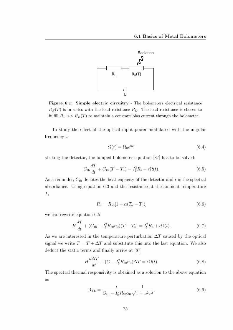
6.1 Basics of Metal Bolometers
Figure 6.1: Simple electric circuitry - The bolometers electrical resistance
RB(T ) is in series with the load resistance RL. The load resistance is chosen to
fulfill RL >> RB(T ) to maintain a constant bias current through the bolometer.
To study the effect of the optical input power modulated with the angular
frequency ω
Ω(t) = Ω0eiωt (6.4)
striking the detector, the lumped bolometer equation [87] has to be solved:
CthdT
dt+Gth(T − Ta) = I2
bRb + εΩ(t). (6.5)
As a reminder, Cth denotes the heat capacity of the detector and ε is the spectral
absorbance. Using equation 6.3 and the resistance at the ambient temperature
Ta
Ra = Rb0[1 + α(Ta − T0)] (6.6)
we can rewrite equation 6.5
HdT
dt+ (Gth − I2
bRb0α0)(T − Ta) = I2bRa + εΩ(t). (6.7)
As we are interested in the temperature perturbation ∆T caused by the optical
signal we write T = T + ∆T and substitute this into the last equation. We also
deduct the static terms and finally arrive at [87]
Hd∆T
dt+ (G− I2
bRb0α0)∆T = εΩ(t). (6.8)
The spectral thermal responsivity is obtained as a solution to the above equation
as
RTh =ε
Gth − I2bRb0α0
1√1 + ω2τ 2
, (6.9)
75

6. METAMATERIAL METAL BOLOMETER
where the effective time constant is
τ =Cth
Gth − I2bRb0α0
. (6.10)
When characterizing the performance of a bolometer, often the electrical respon-
sivity < is used:
< = dUb
dΩ(t)= dUb
dR· dRdT· dTdΩ(t)
(6.11)
= Ib ·Rb0α0 ·RTh. (6.12)
Inserting equation 6.9 finally results in
< =εIbRb0α0
Gth − I2bRb0α0
· 1√1 + ω2τ 2
. (6.13)
Due to the effect of the electro-thermal feedback mechanism, the effective ther-
mal conductivity Geff = Gth− I2bRb0α0 differs from the thermal conductivity Gth.
The effect of Joule’s heating also limits the magnitude of the bias current. For a
metal bolometer with α0 > 0, a current of Ib =√Gth/(Rb0α0) leads to a diver-
gence of the responsivity, called the thermal runaway. The magnitude of the bias
current is therefore limited for practical applications to Ib,max ≈ 0.5√Gth/(Rb0α0)
[88].
6.2 Thermal Characterization of the Bolometer
The thermal conductance Gth is the most important parameter for the evaluation
of the performance of a bolometer. The measurement of the thermal conductance
can be achieved by generating heat in the detector and simultaneously measuring
the increase in temperature. As as heat source, the absorption of thermal radi-
ation could be used. But this bolometric method is rather complicated, because
the accurate measurement of the absorbed optical power is difficult. Another
way to experimentally determine the thermal conductance can be done by the
DC method. Here the device is biased with a constant current and the effect
of the dissipation of electrical power within the bolometer is exploited as a heat
source. Using the relation
Gth∆T = I2bRb (6.14)
76

6.2 Thermal Characterization of the Bolometer
combined with the temperature dependence of the resistance, one obtains
Rb ·Rb0
Rb −Rb0
= −αGI2.. (6.15)
Using this relation, a measurement of the resistance of the bolometer as a function
of the bias current squared, reveals the factor α/Gth.
To deduce the thermal conductance from the above measurement, the TCR
α must be known to deduce the thermal conductance Gth which can be easily
obtained from a separate measurement [89]. The device is externally heated,
starting from the temperature T0 ,and the change in resistance ∆R = R(T )−R0
together with the temperature T > T0 is logged. Plotting the function 6.1
∆R = α(T − T0) (6.16)
reveals the TCR α by linear curve fitting.
The DC method has some major drawback. When evaluating Gth from equa-
tion 6.15, its accuracy is very sensitive to changes in the reference temperature T0.
Due to small denominator Rb −Rb0, tiny changes in the environmental tempera-
ture lead to a variation within Rb and in turn to a large error in determining Gth.
For an accurate measurements the reference temperature in the vicinity of the
detector should therefore be monitored carefully using an additional temperature
sensor.
To overcome these drawbacks, we have used the so-called 3ω method for the
characterization of our bolometer. In addition, this method also allows the char-
acterization of the dynamical behavior of the bolometer, i.e. the time constant
τ .
The 3ω Method
The concept of the 3ω method is based on using an AC current to feed a thin metal
strip that acts both as a heater and temperature sensor [90, 91]. The current is
sinusoidally oscillating at the fundamental frequency ω. Due to the dissipation
of electrical energy within the metal strip, the temperature is oscillating at twice
the fundamental frequency 2ω. The linear dependence of the strips resistance on
the temperature 6.1 leads to an oscillation of the resistance with the frequency
2ω. This in turn leads to a voltage oscillation across the strip having a component
77

6. METAMATERIAL METAL BOLOMETER
at 3ω. Measuring this voltage oscillation allows one to characterize the thermal
environment of the heater, namely the thermal insulation or thermal conductance
[92, 93]. In addition, this method also allows the determination of the thermal
capacity of the heated material when also the frequency dependence of the voltage
oscillation is measured [94].
As shown in reference [95], this principle can be applied to the characteriza-
tion of a metal bolometer. They have used a combination of a constant current
together with an oscillating current. Here we use their derivation but use only
an AC current Ib = I · cos(ωt) to bias the bolometer. The heat balance equation
then reads
CthdT
dt+ [Gth − I2 cos2(ωt) · α0Rb0] · (T − T0) =
I2Rb0
2cos(2ωt). (6.17)
The temperature oscillation ∆T = T − T0 can be solved analytically from the
above equation as [95]
∆T = e−k(t)
∫ek(t) · I2 Rb0
2Cthcos(2ωt)dt+ c0e
−k(t) (6.18)
where k(t) is given by
k(t) =1
Cth(Gth −
1
2· I2α0Rb0)t− I2α0
Rb0
4Cthωsin(2ωt). (6.19)
The integration constant c0 depends on the initial condition and quickly vanishes
in several thermal time constants. It is therefor valid to assume a steady-state con-
dition where c0 = 0. Fur the further discussion we set Geff = Gth− 1/2 · I2α0Rb0
and neglect the last term in 6.19 to obtain the time dependent temperature os-
cillation
∆T =I2Rb0
2Geff
√1 + (2ωτ)
cos(2ωt+ φ) (6.20)
with the time constant τ = Cth/Geff .
The voltage across the bolometer then is given by
Ub(t) = Ib(t) ·Rb(t) (6.21)
= I cos(ωt) ·Rb0(1 + α0∆T ) (6.22)
78

6.3 Experimental Setup
and together with 6.20 we have finally
Ub(t) = Rb0I cos(ωt) +I3R2
b0α0
4Geff
√1+(2ωτ)2
cos(ωt+ φ) (6.23)
+I3R2
b0α0
4Geff
√1 + (2ωτ)2︸ ︷︷ ︸
Ub,3ω
cos(3ωt+ φ). (6.24)
The frequency component of the voltage Ub,3ω that oscillates with three times the
fundamental frequency is of special interest. Its magnitude directly relates to the
effective thermal conductance Geff and from its frequency dependent behavior
we can also determine the effective time constant τ .
6.3 Experimental Setup
The characterization of the metamaterial bolometer was done with the experi-
mental setup sketched in figure 6.2. For the optical characterization we have used
an optical parametric oscillator (OPO) 1 as a tunable narrow band light source.
The tuning range of the OPO is from 1.2 µm up to 1.8 µm. The beam passes
a half-wave plate and a polarizer. By turning the half-wave plate and keeping
the polarizer position fixed, the power of the OPO impinging on the sample can
be adjusted. In addition, by turning the polarizer, the polarization angle can be
arbitrarily adjusted. This allows a polarization dependent spectroscopy of the
sample without the need to turn the sample itself.
To monitor and set the appropriate power on the sample, a movable power
meter can be placed right after the polarizer which is removed right before the
measurement. The beam from the OPO is then focussed on the sample to a
spot size of approximately 30 µm, using a lens L. The sample is placed inside
a vacuum chamber with windows at both sides to allow the transmission of the
laser beam. The chamber is mounted on a translation stage that allows for a
manual adjustment of the position of the sample relative to the laser beam. A
feed-through wiring allows the electrical connection of the sample to the outside
world. In addition, a rotary-vane vacuum pump is connected to the chamber for
an evacuation of the chamber. A camera allows an imaging of the sample and
1Inspire, Spectra-Physics
79

6. METAMATERIAL METAL BOLOMETER
Figure 6.2: Sketch of the experimental setup -
provides an easy way to control the position of the sample relative to the laser
beam.
The electrical measurement of the bolometer and the logging of the corespond-
ing data is implemented using a lock-in amplifier 1. We used the amplifier’s own
build in oscillator to feed a current through the bolometer. A load resistor RL,
much larger then the bolometers resistance, was used to provide an AC current
source for the four-terminal sensing of the bolometers resistance. By using an
AC current, we circumvent effects of electromigration. The very thin bolometer
wires are expected to be very sensitive to effects of electromigration associated
with a DC current [96, 97]. The voltage drop over the bolometer is then measured
using the amplifier input. In combination with a computer that is connected via
RS-232 and is running Matlab 2, an easy and automated measurement routine
for the characterization of the bolometer could be implemented.
Resistance Measurement
Measuring the resistance of a simple resistor is normally done using a multimeter
with two leads. The multimeter forces a test current through the leads and the
1SR 830, Stanford Research Systems2Matlab, The MathWorks, Inc.
80

6.3 Experimental Setup
resistor and then reads the voltage drop across the wires and calculates the resis-
tance according to Ohm’s law. The measured resistance is therefore the sum of
the lead resistance, the resistance of the resistor itself, and the contact resistance
of the leads. For larger resistors, the result is dominated by the resistance of the
resistor. But if the resistance to be measured is low (in the range of 100Ω or lower
[98]), there is a problem due to inaccurate readings because the resistance of the
leads can not be neglected anymore. The drawbacks of this so called two-wire
method can be overcome with the four-wire or four-terminal sensing method.
Here, two wires are used to feed the test current through the resistor under test.
A second pair of leads, the sense leads, is used to measure the voltage drop across
the device under test. This method is also suitable for measuring sheet resistance
of very thin films. In our experiments, the resistance of the bolometer structure
is measured using a pad geometry that is suitable for measurements with the
four-wire method.
Four-Terminal Sensing Setup
To see why the four-wire setup drops the resistance of leads and contacts, the ge-
ometry of the contact pads and the equivalent circuit are presented. The bolome-
ter resistance RB is connected in series with the lead and contact resistances,
that are represented by RL1 and RL2. The lead and contact resistance and in-
nenwiderstand RU of the voltage measuring instrument are connected parallel to
the resistance of the bolometer. According to kirchhoffs laws we can write for the
current at the green connection
UB = IB ·RB = (I − IU) ·RB (6.25)
and the voltages in the loop
UB = U + UU1 + UU2 = IU · (RU1 +RU2 +RU) (6.26)
. Setting both equation equal yields
(I − IU) ·RProbe = IU · (RU1 +RU2 +RU) (6.27)
IU = I·RB
RU1+RU2+RU+RB(6.28)
The measured voltage is
U = IU ·RU (6.29)
81

6. METAMATERIAL METAL BOLOMETER
and therefor
U =I ·RB ·RU
RU1 +RU2 +RU +RB
. (6.30)
To see that this is equal to U = I ·RB we write
U = I ·RB · (1− α) (6.31)
and find
α = 1− RU
RU1+RU2+RU+RB(6.32)
= RU1+RU2+RB
RU1+RU2+RU+RB. (6.33)
For a sufficient high innenwiderstand RU we find that α << 1 and therfore
U = I ·RB (6.34)
RB = UI
(6.35)
is valid.
Figure 6.3: Four-terminal sensing - In a): sketch of the pad geometry used to
contact the bolometer structure; b) equivalent circuit of the geometry
82

6.4 Experimental Results
Figure 6.4: Metamaterial metal-based bolometer - Scanning electron micro-
graphs of one of the fabricated devices in different magnifications as indicated by
the black scale bars. The active area including the connected resonant polarization-
sensitive gold absorber elements is located on a 30 nm thin SiN membrane (black).
The arrows on the right-hand side indicate the orientation of the linear eigen-
polarizations used in the optical experiments in figure 6.5. (figure and caption
from [99])
6.4 Experimental Results
In figure 6.4 the corresponding bolometer design is shown. The scanning electron
micrographs show the 40nm thin gold nanostructures that are placed on a 30nm
thin, commercial available silicon-nitride (SiN) membrane 1. Fabrication of the
structure was done using the electron-beam lithography process with a two-resist
system. This measure enhances the undercutting effect on the thin membrane and
improves the lift-off process. The membrane has a footprint of 100 µm × 100 µm
and serves for mechanical support. It also provides a good thermal isolation of the
bolometer structure as it strongly reduces the conduction of heat. Thin films of
silicon-nitride or silicon-dioxide are often used in the context of microbolometers,
thermal detectors or microcaloriometers, as these materials provide good thermal
insulation and good mechanical stability [64, 100, 101, 102, 103, 104]. The sensor
part, consisting of a grid array of modified split-ring resonators, is placed in
the middle of the membrane and has a footprint of 35 µm. This array is then
electrically connected to four large bond pads in the outer region of the substrate
which is supported by the underlying silicon substrate. The substrate is finally
glued in on an IC-carrier and processed as already described in the materials and
methods section in chapter 3.
1Silson Ltd. UK
83

6. METAMATERIAL METAL BOLOMETER
Figure 6.5: Optical and electrical characterization of the metamaterial
bolometer - (a), Measured (solid curves) and calculated (dashed curves) extinction
spectra for the two linear polarizations indicated by the blue and red arrows in fig-
ure 6.4. (b), Measured (dots) and calculated (dashed) bolometer responsivity for an
rms current of 50 µA. The calculated responsivity is obtained from the calculated
absorbance spectra and the measured thermal conductance G. (c), The thermal
conductance and the bolometer time constant are obtained from the depicted mea-
sured voltage at the third harmonic of the modulation frequency measured versus
modulation frequency. The bolometer time constant of 134 µs = 1/(2 · 2π · 596 Hz)
results from the -3 dB decay (see left vertical logarithmic scale and dashed lines).
(d), Corresponding measured phase.(figure and caption from [99])
84

6.4 Experimental Results
The first step towards the full characterization of the bolometer is the mea-
surement of the extinction which is the negative decadic logarithm of the intensity
transmittance spectra. Using the standard Fourier-transform spectrometer, the
spectra are obtained for light impinging from the SiN membrane side normal to
the membrane. Interestingly, the measurements have revealed two linear eigen-
polarizations that are diagonally oriented with respect to the SRR arms. In figure
6.5 (a) the measured spectra for the two eigen-polarizations is plotted. The color
coding of the curves corresponds to the arrows in figure 6.4.
These measurements are the basis for the further optical characterization. The
extinction spectra clearly show a spectral and polarization dependent resonance.
To reveal the connected absorption, a direct measurement of the spectral and
polarization dependent responsivity of the bolometer is needed. The sample is
therefor placed inside the vacuum chamber of the setup providing pre-vacuum
conditions with a pressure of about 1 mbar. This prevents the heat transport via
air and enhanced the responsivity of the bolometer.
In figure 6.5 (b), the measured responsivity (dots) versus wavelength, for a
bias current of I = 50 µA that oscillates at 1 kHz, is presented. The laser power
of the OPA, impinging on the sample, is adjusted to 50 µW for all wavelengths
and polarization directions. One can clearly see the pronounced resonance for one
linear polarization (blue dots), whereas there is very little signal found for the
orthogonal linear polarization (red dots). These results show that the bolometer
signal is governed by light absorption in the metal nanostructure and a subsequent
heating of the metal. The corresponding bolometer voltage change is induced by
the resistance change of the metal.
To fully characterize the bolometer according to the responsivity 6.13, the
TCR α0, the effective thermal conductance Geff and the detector’s time constant
need to be determined. The measurement of the TCR was done by heating the
bolometer using a hot plate and simultaneously measure the temperature of the
plate and the resistance of the bolometer 6.6. From this fit we deduce a TCR of
α0 = 0.0024 1/K. This value matches the values reported in literature for thin
gold films of similar thickness [105].
By measuring the third harmonic component Ub,3ω 6.24 of the bolometer volt-
age versus the modulation frequency, the effective thermal conductance Geff =
4.85 · 10−6 W/K can be deduced. For the determination of the time constant we
85

6. METAMATERIAL METAL BOLOMETER
Figure 6.6: Measurement of the TCR - Plot of the measured resistance change
∆R = R − R0 versus temperature change ∆T = T − T0 of the bolometer. The fit
to the measured data reveals the TCR α0 = 0.0024 1/K.
used the analogy of an thermal low pass filter. From equation 6.24 we can see,
that the third harmonic voltage resembles the voltage of an RC-circuit that acts
as an low-pass filter
Ub,3ω(ω) = Ub,3ω ·1√
1 + ω2τ 2/4(6.36)
where Ub,3ω = I3R2b0α0/(4Geff). When plotting the gain in dB as
Gain = 20 · log
(Ub,3ω(ω)
Ub,3ω
)(6.37)
we can get the time constant from the -3dB point within the bode plot. This
cutoff frequency corresponds to fc = 1/(2π2τ). The bolometer time constant
is determined as 134 µs. We have also plotted the phase of the voltage signal.
The phase shift of -45 degrees corresponds very well to the cut-off frequency, in
accordance with the theory of a low-pass filter. These results are shown in figure
6.5(c),(d).
The bolometer performance is not only characterized by its responsivity but
also by the noise of the bolometer and its read-out electronics. Our experimen-
tal setup was not optimized for a low noise measurement and an experimental
characterization of the noise characteristics was not done. In the context of thin-
metal-film bolometer it is known that ultimate performance is limited by the
Johnson-noise of the metals resistance [77]. When we assume a Johnson-noise-
limited performance, the resistance of our bolometer of R = 300 Ω under room-
86

6.4 Experimental Results
temperature operation results in a noise-equivalent power of 6.7 · 10−10W/√
Hz
allowing the detection of faint signals in the range of nW.
The measured data is the basis for our further theoretical studies. Using the
software package CST Microwave Studio, numerical calculations were conducted
to evaluate the spectral tuning capabilities of the metamaterial bolometer con-
cept. For the simulations of the metal behavior the free-electron Durde model
with a plasma frequency ωpl = 1.37 · 1016 rad/s was used. The damping was
accounted using a collision frequency of ωcol = 2.2 · 1014 rad/s. From the electron
micrographs in figure 6.4, the geometrical parameters could be extracted. The
gold thickness for the simulations was chosen as 40 nm in accordance with the
experiment. The refractive index of the 30 nm thin SiN membrane was set to
n = 1.96. In figure 6.5 (a), the calculated extinction spectra are shown as dashed
curves. From these data, we calculate the spectral absorbance ε = 1 − T − R
using the corresponding transmission T and reflection spectra R from Microwave
Studio. This finally allows the calculation of the spectral responsivity of the
bolometer using equation 6.13 together with the previously experimentally deter-
mined values. In figure 6.5 (b) the results are plotted as dashed lines. Obviously,
the spectral resonant behavior as well as the polarization dependence are quali-
tatively well reproduced.
The good qualitative agreement is the starting point for the evaluation of the
tunability of the resonant bolometer response. A broad spectral tuning range
is key for the implementation of broadband spectrometers. For the theoretical
investigation, we scale the lateral features of the structure while keeping the
metal thickness constant. This measure fixes the bolometers thermal mass per
unit area. In figure 6.7 the corresponding calculations of the absorbance ε are
presented where the linear polarization is oriented relative to the structure as
indicated by the blue arrow in figure 6.4. The right configuration corresponds to
the feature size that was used to calculate the responsivity of our experimentally
fabricated bolometer. Starting from this configuration we increased the lateral
features in steps of factors of two. As can be seen, a tuning between roughly 1
µm up to 10 µm wavelength is possible.
87

6. METAMATERIAL METAL BOLOMETER
Figure 6.7: Calculations on bolometer tunability - For reference, the highest
frequency resonance corresponds to the parameters of figure 6.5. For the other
three structures, all lateral dimensions are increased in steps of factors of two
(see insets), while fixing the metal thickness, hence fixing the bolometer thermal
mass. Importantly, the fundamental absorber resonances can be shifted towards
significantly longer wavelengths, while maintaining the peak absorbance. (figure
and caption from [99])
Figure 6.8: Envisioned bolometer array architecture - This concept allows
for integrated broadband spectroscopy and polarimetry without the need for any
external dispersive element or any polarizer. (figure and caption from [99])
88

6.4 Experimental Results
6.4.1 Conclusions
The proof-of-concept of a metamaterial metal-based bolometer takes advantage
of the resonant absorption accompanied by the excitation of plasmonic resonances
within gold nanostructures. That way, a spectral and/or polarization filter can
be built into the bolometer without the need of external dispersive elements. On
this basis, an integrated broadband metamaterial metal-based bolometer spec-
trometer array can be envisioned, as illustrated in figure 6.8. The presence of the
rotated elements would simultaneously allow for analyzing the polarization state
of light.
89

6. METAMATERIAL METAL BOLOMETER
90

7
Conclusions and Outlook
The first part of the experimental work presented in this thesis focussed on the
second-harmonic generation from gold split-ring resonator arrays. Earlier work on
this topic has revealed a strong nonlinear optical response from this metamaterial
building block [45, 46, 47]. With these results as a starting point, we explored the
idea of Pendry [3], who pointed out the possible extraordinary nonlinear optical
response of a SRR having a nonlinear optical material placed into the gap region of
the SRR. The concentration of the electric field within the gap region might lead
to an enhanced nonlinear response. We slightly modified this idea, and placed
the gold SRR on a substrate possessing itself a strong nonlinear optical response
of second order, namely gallium arsenide (GaAs). The orientation of the SRR
relative to the GaAs crystallographic axes and the incident light polarization
was varied systematically. As a result, we did find a configuration where the
overall signal strength of the SHG was approximately a factor of 25 times larger
than those from SRR arrays on glass substrates, when referenced to the same
incident laser intensity. In addition, an analyzation of the polarization of the
emitted SHG light revealed a nonlinear contribution that originates specifically
from the interplay of the local fields of the split-ring resonators with the bulk
GaAs second-order nonlinear-susceptibility tensor. These results were also in
good agreement with a theoretical modeling of this system. A simple near-field
simulation of the resonantly excited SRR was used as the source for a calculation
of the nonlinear polarization of second order within the GaAs crystal. Through
a spatial averaging of this polarization over the whole unit cell, we were able to
identify the main component of the nonlinear polarization contributing to the
91

7. CONCLUSIONS AND OUTLOOK
measured SHG signal.
For the next experiment, a new setup suitable for nonlinear optical spec-
troscopy was build. The setup used an optical parametric oscillator as a tunable
light source and consisted of a sample and a reference arm. While previous
second-harmonic-generation experiments on gold split-ring-resonator arrays were
all limited to a fixed excitation wavelength [45, 46, 47], using this new setup,
a full second-harmonic spectroscopy study on SRR arrays could be conducted.
For the set of samples, the technique of a lithographic tuning of the spectral
resonance position of the SRR arrays was employed. This technique was already
introduced by Klein et al. [45] to overcome the limitation of the fixed excitation
wavelength used in their experiment. Here, this tuning was used to study the
role of the relative spectral positions of the fundamental magnetic resonance and
the higher order resonances of gold SRR arrays on glass substrates on the process
of second-harmonic generation. The measured nonlinear spectroscopic data on a
first set of samples, where the size of the SRR was scaled, revealed pronounced
resonances. The SHG maximum shifts when the resonance positions of the SRR
is changed through the lithographic tuning. To clarify the role of the higher-order
resonances on the SHG signal, a second set of samples was produced. Here, the
shape of the SRR was varied in such a way, that the higher-order resonances
of the SRR stay spectrally fixed and only the fundamental magnetic resonance
position of the SRR is shifted. The corresponding second-harmonic generation
spectra again reveals resonances. However, the SHG maximum correlates with
the position of the fundamental SRR resonance and not with the position of the
higher-order resonances. This is interpreted as an indication for the fundamental
SRR resonance to act as the nonlinear source while higher-order SRR resonances
merely reabsorb the generated vertically polarized SHG. The measured spectro-
scopic data helped in clarifying the role of the higher-order resonances and also
provide a sensitive future testing ground for microscopic theories of the underlying
physical mechanisms.
In the third experiment on second-harmonic generation from SRR arrays, we
have studied the dependence of the conversion efficiency on the lattice constant.
The experiment was motivated by the search for the most efficient configura-
tion for frequency conversion with regard to the spacing between individual SRR
within the array. Intuitively, one might think that the best conversion efficiency
92

is achieved by packing the individual building blocks as dense as possible as this
maximizes the number of nonlinear emitters per unit area. To test this intu-
itive reasoning, a set of samples was fabricated, where the spectral position of
the resonances of each SRR array was kept constant but the distance between
the SRR within each array was systematically modified to change the packing
density. This sample was then characterized using the same second-harmonic
spectroscopy setup as in the earlier experiment. The experimental result revealed
a non-monotonic behavior of the resonant second-order nonlinear conversion ef-
ficiency versus the packing density, rendering the intuitive approach for efficient
frequency conversion invalid. The maximum conversion efficiency was found for
an intermediate lattice constant. A closer inspection of the experimental data re-
vealed two counteracting effects influencing the overall SHG conversion efficiency.
By bringing the SRRs closer to each other, the SHG intensity rises because of
more nonlinear emitters per unit area. On the other hand, bringing the SRRs
closer also increases the damping of the linear fundamental resonance as can be
seen from the change in linewidth of the corresponding measured linear extinction
spectra. The linewidth enters sensitively into the second-order nonlinear-optical
susceptibility χ(2), a larger damping leads to a smaller resonant χ(2), thus re-
ducing the conversion efficiency when the SRR are brought closer to each other.
Both effects level out a some intermediate lattice constant to provide the maxi-
mum SHG conversion efficiency. Numerical calculations using the discontinuous
Galerkin time-domain method could reproduce the experimental findings well and
allowed to support the qualitative reasoning. These calculations allowed also for
an inspection of the SRR electric near-field at the fundamental excitation wave-
length. We found that an increase of the lattice constant leads to an increase of
the strength of the near and internal fields of the SRR. This leads to a stronger
nonlinear response of the SRR and can explain the initial increase of SHG in-
tensity with increasing lattice constant. Then, for yet larger lattice constants,
this increase is compensated and dominated by the dilution effect, leading to the
observed decrease in SHG signal intensity.
The final experiment aimed on providing a possible application of metamate-
rials. For many metamaterial applications, the loss that is inherently connected
to its plasmonic resonances is an often unwanted by-product. The new concept of
a metamaterial-metal based bolometer uses theses losses to its advantage. While
93

7. CONCLUSIONS AND OUTLOOK
the principle of a metal bolometer is known for more than one century, with the
new concept, an old idea is enhanced by a new technology. A modified gold split-
ring resonator structure was used to not only provide a lithographically tunable
resonant absorption over a broad spectral range, but also to measure the temper-
ature increase due to the absorption of light. Furthermore, the structure is also
polarization sensitive, allowing for an integrated polarization analysis without the
need of external polarizers. The device was fabricated and fully characterized,
optically as well as electrically to proof the spectral and polarization dependent
responsivity.
In summary, the experimental results of this thesis provide a deeper insight
into the mechanisms of nonlinear optics of metamaterials and can be a guide
for future nonlinear optical experiments aiming at achieving large effective op-
tical nonlinearities using metamaterials. In addition, a possible application for
the absorption within metamaterials was demonstrated with the metamaterial
bolometer. Integration of suitable read-out electronics on a chip in combination
with the metamaterial bolometer could be the next step towards implementation
of a microbolometer arrays using metamaterial absorbers.
94

References
[1] V. Veselago, “The electrodynamics of substances with simultaneously neg-
ative values of ε and µ,” Soviet Physics Uspekhi, vol. 10, no. 4, p. 509,
1968.
[2] J. Pendry, “Negative refraction makes a perfect lens,” Physical Review Let-
ters, vol. 85, no. 18, p. 3966, 2000.
[3] J. Pendry, A. Holden, D. Robbins, and W. Stewart, “Magnetism from con-
ductors and enhanced nonlinear phenomena,” IEEE Transactions On Mi-
crowave Theory and Techniques, vol. 47, no. 11, p. 2075, 1999.
[4] R. Shelby, D. Smith, and S. Schultz, “Experimental verification of a negative
index of refraction,” Science, vol. 292, no. 5514, p. 77, 2001.
[5] S. Linden, C. Enkrich, M. Wegener, J. Zhou, T. Koschny, and C. M.
Soukoulis, “Magnetic response of metamaterials at 100 terahertz,” Science,
vol. 306, no. 5700, p. 1351, 2004.
[6] C. Enkrich, M. Wegener, S. Linden, S. Burger, L. Zschiedrich, F. Schmidt,
J. Zhou, T. Koschny, and C. Soukoulis, “Magnetic metamaterials at
telecommunication and visible frequencies,” Physical Review Letters,
vol. 95, no. 20, p. 203901, 2005.
[7] V. M. Shalaev, “Transforming light,” Science, vol. 322, no. 5900, p. 384,
2008.
[8] J. Pendry, D. Schurig, and D. Smith, “Controlling electromagnetic fields,”
Science, vol. 312, no. 5781, p. 1780, 2006.
95

REFERENCES
[9] U. Leonhardt, “Optical conformal mapping,” Science, vol. 312, no. 5781,
p. 1777, 2006.
[10] T. Ergin, N. Stenger, P. Brenner, J. B. Pendry, and M. Wegener, “Three-
dimensional invisibility cloak at optical wavelengths,” Science, vol. 328,
no. 5976, pp. 337–339, 2010.
[11] C. Soukoulis and M. Wegener, “Past achievements and future challenges
in the development of three-dimensional photonic metamaterials,” Nature
PhotonicsPhoton., vol. 5, no. 9, p. 523, 2011.
[12] N. Landy, S. Sajuyigbe, J. Mock, D. Smith, and W. Padilla, “Perfect meta-
material absorber,” Physical Review Letters, vol. 100, no. 20, p. 207402,
2008.
[13] N. Liu, M. Mesch, T. Weiss, M. Hentschel, and H. Giessen, “Infrared perfect
absorber and its application as plasmonic sensor,” Nano Letters, vol. 10,
no. 7, p. 2342, 2010.
[14] A. Tittl, P. Mai, R. Taubert, D. Dregely, N. Liu, and H. Giessen,
“Palladium-based plasmonic perfect absorber in the visible wavelength
range and its application to hydrogen sensing,” Nano Letters, vol. 11, no. 10,
p. 4366, 2011.
[15] X. Liu, T. Tyler, T. Starr, A. Starr, N. Jokerst, and W. Padilla, “Taming
the blackbody with infrared metamaterials as selective thermal emitters,”
Physical Review Letters, vol. 107, no. 4, p. 045901, 2011.
[16] M. Diem, T. Koschny, and C. Soukoulis, “Wide-angle perfect ab-
sorber/thermal emitter in the terahertz regime,” Physical Review B, vol. 79,
no. 3, p. 033101, 2009.
[17] S. Maier, Plasmonics: Fundamentals and Applications. Springer Berlin
Heidelberg, 2007.
[18] K.-S. Lee and M. El-Sayed, “Gold and silver nanoparticles in sensing and
imaging: sensitivity of plasmon response to size, shape, and metal compo-
sition,” The Journal of Physical Chemistry B, vol. 110, no. 39, p. 19220,
2006. PMID: 17004772.
96

REFERENCES
[19] C. Bohren and D. Huffman, Absorption and scattering of light by small
particles. Wiley Online Library, 1983.
[20] G. Mie, “Beitrage zur optik truber medien, speziell kolloidaler metallosun-
gen,” Annalen der Physik, vol. 330, no. 3, p. 377, 1908.
[21] P. Franken, A. Hill, C. Peters, and G. Weinreich, “Generation of optical
harmonics,” Physical Review Letters, vol. 7, no. 4, p. 118, 1961.
[22] R. Boyd, Nonlinear optics. Academic Press, 2003.
[23] E. Hartmann, An Introduction to Crystal Physics. Cardiff, Wales: Univer-
sity College Cardiff Press, 2001.
[24] F. Brown, R. Parks, and A. Sleeper, “Nonlinear optical reflection from a
metallic boundary,” Physical Review Letters, vol. 14, p. 1029, 1965.
[25] S. Jha, “Theory of optical harmonic generation at a metal surface,” Physical
Review, vol. 140, no. 6A, p. A2020, 1965.
[26] S. Jha, “Nonlinear optical reflection from a metal surface,” Physical Review
Letters, vol. 15, no. 9, p. 412, 1965.
[27] N. Akhmediev, I. Melnikov, and L. Robur, “Second-harmonic generation
by a reflecting metal surface,” Laser Physics, vol. 4, no. 6, p. 1194, 1994.
[28] D. Maystre, M. Neviere, and R. Reinisch, “Nonlinear polarisation in-
side metals: A mathematical study of the free-electron model,” Ap-
plied Physics A: Materials Science & Processing, vol. 39, p. 115, 1986.
10.1007/BF00616828.
[29] J. Rudnick and E. Stern, “Second-harmonic radiation from metal surfaces,”
Physical Review B, vol. 4, p. 4274, 1971.
[30] C. Wang, J. Chen, and J. Bower, “Second harmonic generation from alkali
metals,” Optics Communications, vol. 8, no. 4, p. 275, 1973.
[31] J. Sipe, V. So, M. Fukui, and G. Stegeman, “Second harmonic generation
at metal surfaces,” Solid State Communications, vol. 34, no. 7, p. 523, 1980.
97
REFERENCES
[32] M. Corvi and W. Schaich, “Hydrodynamic-model calculation of second-
harmonic generation at a metal surface,” Physical Review B, vol. 33, no. 6,
p. 3688, 1986.
[33] Y. Zeng, W. Hoyer, J. Liu, S. Koch, and J. Moloney, “Classical theory for
second-harmonic generation from metallic nanoparticles,” Physical Review
B, vol. 79, no. 23, p. 235109, 2009.
[34] J. Liu, M. Brio, Y. Zeng, A. Zakharian, W. Hoyer, S. Koch, and J. Moloney,
“Generalization of the fdtd algorithm for simulations of hydrodynamic non-
linear drude model,” Journal of Computational Physics, vol. 229, no. 17,
p. 5921, 2010.
[35] C. Ciraci, E. Poutrina, M. Scalora, and D. Smith, “Origin of second-
harmonic generation enhancement in optical split-ring resonators,” Physical
Review B, vol. 85, p. 201403, 2012.
[36] D. Smith, W. Padilla, D. Vier, S. Nemat-Nasser, and S. Schultz, “Compos-
ite medium with simultaneously negative permeability and permittivity,”
Physical Review Letters, vol. 84, no. 18, p. 4184, 2000.
[37] K. Busch, G. von Freymann, S. Linden, S. Mingaleev, L. Tkeshelashvili,
and M. Wegener, “Periodic nanostructures for photonics,” Physics Reports-
Review Section of Physics Letters, vol. 444, no. 3-6, p. 101, 2007.
[38] C. M. Soukoulis, “Negative refractive index at optical wavelengths (vol 315,
pg 47, 2007),” Science, vol. 315, pp. 1077–1077, Feb. 2007.
[39] C. Enkrich, R. Perez-Willard, D. Gerthsen, J. Zhou, T. Koschny, C. Souk-
oulis, M. Wegener, and S. Linden, “Focused-ion-beam nanofabrication of
near-infrared magnetic metamaterials,” Advanced Materials, vol. 17, no. 21,
p. 2547, 2005.
[40] K. Fan, A. Strikwerda, H. Tao, X. Zhang, and R. Averitt, “Stand-up
magnetic metamaterials at terahertz frequencies,” Optics Express, vol. 19,
no. 13, p. 12619, 2011.
98
REFERENCES
[41] G. Dolling, C. Enkrich, M. Wegener, J. Zhou, and C. Soukoulis, “Cut-wire
pairs and plate pairs as magnetic atoms for optical metamaterials,” Optics
Letters, vol. 30, no. 23, p. 3198, 2005.
[42] P. Muhlschlegel, H. Eisler, O. Martin, B. Hecht, and D. Pohl, “Resonant
optical antennas,” Science, vol. 308, no. 5728, p. 1607, 2005.
[43] K. Crozier, A. Sundaramurthy, G. Kino, and C. Quate, “Optical antennas:
Resonators for local field enhancement,” Journal of Applied Physics, vol. 94,
no. 7, p. 4632, 2003.
[44] N.-A. Feth, Nonlinear Optics of Planar Metamaterial Arrays and Spec-
troscopy of Individual Photonic Atoms. PhD thesis, Karlsruher Institut fur
Technologie, 2010.
[45] M. Klein, C. Enkrich, M. Wegener, and S. Linden, “Second-harmonic gen-
eration from magnetic metamaterials,” Science, vol. 313, no. 5786, p. 502,
2006.
[46] M. Klein, M. Wegener, N. Feth, and S. Linden, “Experiments on second-
and third-harmonic generation from magnetic metamaterials,” Optics Ex-
press, vol. 15, no. 8, p. 5238, 2007.
[47] N. Feth, S. Linden, M. Klein, M. Decker, F. Niesler, Y. Zeng, W. Hoyer,
J. Liu, S. Koch, J. Moloney, and M. Wegener, “Second-harmonic generation
from complementary split-ring resonators,” Optics Letters, vol. 33, no. 17,
p. 1975, 2008.
[48] S. Kujala, B. Canfield, M. Kauranen, Y. Svirko, and J. Turunen, “Multipole
interference in the second-harmonic optical radiation from gold nanoparti-
cles,” Physical Review Letters, vol. 98, p. 167403, Apr 2007.
[49] B. Canfield, H. Husu, J. Laukkanen, B. Bai, M. Kuittinen, J. Turunen, and
M. Kauranen, “Local field asymmetry drives second-harmonic generation
in noncentrosymmetric nanodimers,” Nano Letters, vol. 7, no. 5, p. 1251,
2007.
99

REFERENCES
[50] W. Fan, S. Zhang, K. Malloy, S. Brueck, N. Panoiu, and R. Osgood, “Second
harmonic generation from patterned gaas inside a subwavelength metallic
hole array,” Optics Express, vol. 14, no. 21, p. 9570, 2006.
[51] S. Kim, J. Jin, Y. Kim, I. Park, Y. Kim, and S. Kim, “High-harmonic gen-
eration by resonant plasmon field enhancement,” Nature, vol. 453, no. 7196,
p. 757, 2008.
[52] F. Niesler, N. Feth, S. Linden, J. Niegemann, J. Gieseler, K. Busch, and
M. Wegener, “Second-harmonic generation from split-ring resonators on a
gaas substrate,” Optics Letters, vol. 34, no. 13, p. 1997, 2009.
[53] H. Day, A. Christou, and A. Macpherson, “Interdiffusion and schottkybarri-
erheight variations in au-w(ti)/ngaas contacts,” Journal of Vacuum Science
& Technology, vol. 14, no. 4, p. 939, 1977.
[54] W. Stremow and E. Cook, “Compilation of energy band gaps in elemental
and binary compound semiconductors and insulators,” Journal of Physical
and Chemical Reference Data, vol. 2, no. 163, 1973.
[55] F. Niesler, N. Feth, S. Linden, and M. W., “Second-harmonic optical spec-
troscopy on split-ring-resonator arrays,” Optics Letters, vol. 36, no. 9,
p. 1533, 2011.
[56] S. Linden, F. Niesler, J. Forstner, Y. Grynko, T. Meier, and M. Wegener,
“Collective effects in second-harmonic generation from split-ring-resonator
arrays,” Physical Review Letters, vol. 109, p. 015502, 2012.
[57] M. Decker, N. Feth, C. Soukoulis, S. Linden, and M. Wegener, “Retarded
long-range interaction in split-ring-resonator square arrays,” Physical Re-
view B, vol. 84, no. 8, p. 085416, 2011.
[58] R. Wood, “On a remarkable case of uneven distribution of light in a diffrac-
tion grating spectrum,” Proceedings of the Physical Society of London,
vol. 18, no. 1, p. 269, 1902.
[59] I. Sersic, M. Frimmer, E. Verhagen, and A. Koenderink, “Electric and mag-
netic dipole coupling in near-infrared split-ring metamaterial arrays,” Phys-
ical Review Letters, vol. 103, no. 21, p. 213902, 2009.
100

REFERENCES
[60] J. Hesthaven and T. Warburton, Nodal Discontinuous Galerkin Methods:
Analysis, Algorithms, and Applications. Springer-Verlag, Berlin, 2008.
[61] K. Stannigel, M. Konig, J. Niegemann, and K. Busch, “Discontinuous
galerkin time-domain computations of metallic nanostructures,” Optics Ex-
press, vol. 17, no. 17, p. 14934, 2009.
[62] A. Akhiezer, I. Akhiezer, R. Polovin, A. Sitenko, and K. Stepanov, Plasma
electrodynamics. Volume I. Linear theory. Pergamon Press, New York,
1975.
[63] Hamamatsu, Characteristics and use of infrared detectors.
[64] F. Voelklein, Thermal-Based Microsensors. Springer Berlin Heidelberg,
2006.
[65] P. Richards, “Bolometers for infrared and millimeter waves,” Journal of
Applied Physics, vol. 76, no. 1, p. 1, 1994.
[66] M. Golay, “A pneumatic infra-red detector,” Review of Scientific Instru-
ments, vol. 18, no. 5, p. 357, 1947.
[67] S. Langley, “The bolometer and radiant energy,” in Proceedings of the
American Academy of Arts and Sciences, vol. 16, p. 342, JSTOR, 1880.
[68] E. Archbold, “An evaporated gold bolometer,” Journal of Scientific Instru-
ments, vol. 34, no. 6, p. 240, 1957.
[69] W. Blevin and W. Brown, “Large-area bolometers of evaporated gold,”
Journal of Scientific Instruments, vol. 42, no. 1, p. 19, 1965.
[70] C. Aiken, W. Carter, and F. Phillips, “The production of film type bolome-
ters with rapid response,” Review of Scientific Instruments, vol. 17, no. 10,
p. 377, 1946.
[71] D. Ball, Field guide to spectroscopy. SPIE Press, 2006.
[72] M. Galeazzi and D. McCammon, “Microcalorimeter and bolometer model,”
Journal of Applied Physics, vol. 93, no. 8, p. 4856, 2003.
101

REFERENCES
[73] J. L. IV and J. L. V, A Heat Transfer Textbook, vol. 4. Phlogiston Press,
1961.
[74] I. T. AG, “Thermal resistance theory and practice,” tech. rep., Infineon
technologies, 2000.
[75] S. Stetson, Pspice Modelling and Parametric Study of Microbolometer Ther-
mal Detectors. PhD thesis, US Navy Naval Postgraduate School, 2001.
[76] Y.-M. Chen, J.-S. Shie, and T. Hwang, “Parameter extraction of resistive
thermal sensors,” Sensors and Actuators A: Physical, vol. 55, no. 1, p. 43,
1996. International Workshop on Thermal Investigations of ICs and Mi-
crostructures (THERMINIC Workshop).
[77] K. Liddiard, “Thin-film resistance bolometer ir detectors,” Infrared Physics,
vol. 24, no. 1, p. 57, 1984.
[78] J. Talghader, “Thermal and mechanical phenomena in micromechanical
optics,” Journal of Physics D: Applied Physics, vol. 37, no. 10, p. R109,
2004.
[79] M. Stockman, “Criterion for negative refraction with low optical losses
from a fundamental principle of causality,” Physical Review Letters, vol. 98,
no. 17, p. 177404, 2007.
[80] P. Kinsler and M. McCall, “Causality-based criteria for a negative refractive
index must be used with care,” Physical Review Letters, vol. 101, no. 16,
p. 167401, 2008.
[81] N. Meinzer, Coupling Plasmonic Metamaterials to Single-Quantum-Well
Gain. PhD thesis, Karlsruher Institut fur Technologie, 2011.
[82] Y. Avitzour, Y. Urzhumov, and G. Shvets, “Wide-angle infrared absorber
based on a negative-index plasmonic metamaterial,” Physical Review B,
vol. 79, no. 4, p. 045131, 2009.
[83] H.-T. Chen, J. Zhou, J. O’Hara, F. Chen, A. Azad, and A. Taylor, “Antire-
flection coating using metamaterials and identification of its mechanism,”
Physical Review Letters, vol. 105, no. 7, p. 073901, 2010.
102

REFERENCES
[84] M. Knight, H. Sobhani, P. Nordlander, and N. Halas, “Photodetection with
active optical antennas,” Science, vol. 332, no. 6030, p. 702, 2011.
[85] G. Shvets, S. Trendafilov, J. Pendry, and A. Sarychev, “Guiding, focusing,
and sensing on the subwavelength scale using metallic wire arrays,” Physical
Review Letters, vol. 99, no. 5, p. 053903, 2007.
[86] N. Verellen, Y. Sonnefraud, H. Sobhani, F. Hao, V. Moshchalkov,
P. Van Dorpe, P. Nordlander, and S. Maier, “Fano resonances in individual
coherent plasmonic nanocavities,” Nano Letters, vol. 9, no. 4, p. 1663, 2009.
[87] J.-S. Shie, Y.-M. Chen, M. Ou-Yang, and B. Chou, “Characterization and
modeling of metal-film microbolometer,” Microelectromechanical Systems,
Journal of, vol. 5, no. 4, p. 298, 1996.
[88] E. Monticone, L. Boarino, G. Lerondel, R. Steni, G. Amato, and V. Lac-
quaniti, “Properties of metal bolometers fabricated on porous silicon,” Ap-
plied Surface Science, vol. 142, no. 1, p. 267, 1999.
[89] P. Eriksson, J. Andersson, and G. Stemme, “Thermal characterization of
surface-micromachined silicon nitride membranes for thermal infrared de-
tectors,” Journal of Microelectromechanical Systems, vol. 6, no. 1, p. 55,
1997.
[90] D. Cahill and R. Pohl, “Thermal conductivity of amorphous solids above
the plateau,” Physical Review B, vol. 35, no. 8, p. 4067, 1987.
[91] Cahill, Katiyar, and Abelson, “Thermal conductivity of α-si:h thin films,”
Physical Review B, vol. 50, no. 9, p. 6077, 1994.
[92] C. Dames and G. Chen, “1ω, 2ω, and 3ω methods for measurements of ther-
mal properties,” Review of Scientific Instruments, vol. 76, no. 12, p. 124902,
2005.
[93] T. Borca-Tasciuc, A. Kumar, and G. Chen, “Data reduction in 3ω method
for thin-film thermal conductivity determination,” Review of Scientific In-
struments, vol. 72, no. 4, p. 2139, 2001.
103

REFERENCES
[94] A. Jain and K. E. Goodson, “Measurement of the thermal conductivity
and heat capacity of freestanding shape memory thin films using the 3ω
method,” Journal of Heat Transfer-Transactions of the Asme, vol. 130,
no. 10, p. 102402, 2008.
[95] M. Ou-Yang, C. Sheen, and J. Shie, “Parameter extraction of resistive
thermal microsensors by ac electrical method,” IEEE Transactions On In-
strumentation and Measurement, vol. 47, no. 2, p. 403, 1998.
[96] F. O. Hadeed and C. Durkan, “Controlled fabrication of 1-2 nm nanogaps
by electromigration in gold and gold-palladium nanowires,” Applied Physics
Letters, vol. 91, no. 12, p. 123120, 2007.
[97] B. Stahlmecke, Elektromigration in Gold und Silber Nanostrukturen. PhD
thesis, Universitat Duisburg-Essen, 2008.
[98] I. Keithley Instruments, Low Level Measurements Handbook. Keithley In-
struments, Inc., 6th edition ed., 2011.
[99] F. Niesler, J. Gansel, S. Fischbach, and M. Wegener, “Metamaterial metal-
based bolometers,” Applied Physics Letters, vol. 100, no. 20, p. 203508,
2012.
[100] F. Gonzalez, B. Ilic, and G. Boreman, “Antenna-coupled microbolometers
on a silicon-nitride membrane,” Microwave and Optical Technology Letters,
vol. 47, no. 6, p. 546, 2005.
[101] B. Zink and F. Hellman, “Specific heat and thermal conductivity of low-
stress amorphous si-n membranes,” Solid State Communications, vol. 129,
no. 3, p. 199, 2004.
[102] B. Revaz, B. Zink, D. O’Neil, L. Hull, and F. Hellman, “Numerical simula-
tion of the heat transfer in amorphous silicon nitride membrane-based mi-
crocalorimeters,” Review of Scientific Instruments, vol. 74, no. 10, p. 4389,
2003.
[103] M. Ahn, Y.-H. Han, and S. Moon, “A novel infrared absorbing structure for
uncooled infrared detector,” Current Applied Physics, vol. 7, no. 6, p. 617,
2007.
104

REFERENCES
[104] M. Burzo, P. Komarov, and P. Raad, “Thermal transport properties of
gold-covered thin-film silicon dioxide,” IEEE Transactions On Components
and Packaging Technologies, vol. 26, no. 1, p. 80, 2003.
[105] M. Adamov, B. Perovic, and T. Nenadovic, “Electrical and structural prop-
erties of thin gold films obtained by vacuum evaporation and sputtering,”
Thin Solid Films, vol. 24, no. 1974, p. 89, 1974.
105

REFERENCES
106

Acknowledgments
The last words of this thesis are dedicated to thanking all the people who con-
tributed to the success of this work.
First and foremost, I thank my supervisor Prof. Dr. Martin Wegener for
providing me an excellent environment for research. I value the opportunity he
gave to me to work on an interesting scientific topic in his group. He also allowed
space for my own ideas and helped them to grow in a successful direction through
his profound knowledge and vast experience. His professionalism is an inspiring
example I appreciated during working with him.
I also thank Prof. Dr. Stefan Linden who introduced me into the field of
metamaterials. His experimental and theoretical knowledge he shared with me
allowed me to handle difficulties in the daily lab work. I enjoyed reflecting new
ideas in the numerous fruitful discussions we had.
I thank Prof. Dr. Kurt Busch for not only agreeing to co-referee my thesis but
also for the successful collaboration with his group, which lead to an interesting
publication in the field of nonlinear optics of metamaterials.
Regarding the collaboration during my thesis, I also thank Prof. Dr. Torsten
Meier and his group from Paderborn for their theoretical support on our joint
publication.
I also want to thank those numerous helping hands for everyday problems.
The electronics workshop with Helmuth Lay and Werner Gilde, and the group
technician Johann Westhauser were of great help and their rapid response will stay
in my memory. The secretary of the Institute of Applied Physics , Renate Helfen,
impressed me with her friendly and straightforward way of solving problems and
getting things done.
Special thanks goes to Dr. Nils Feth and Dr. Mathias Ruther for their
assistance in all technical concerns of electron-beam lithography, lab equipment
107

REFERENCES
and beyond. In addition, I also thank all the members of the Wegener group for
their support and inspirations.
Finally, I wish to express my utmost thanks to all my friends, the members of
my family, as well as my girl-friend Andrea for their continuing love and support
over the years.
108


![Improved Split-Ring Resonator for Microfluidic split ring.pdf · Digital Object Identifier 10.xxxx/TMTT.2012.xxxxxxx cavities [13], dielectric resonators [14], hairpin cavities [15],](https://static.fdocuments.us/doc/165x107/5f5fc1cb39934d1bd573d643/improved-split-ring-resonator-for-microfluidic-split-ringpdf-digital-object-identiier.jpg)