Nonlinear diffraction in orientation-patterned …...Nonlinear diffraction in orientation-patterned...
10
Nonlinear diffraction in orientation-patterned semiconductors Pawel Karpinski, 1,2,* Xin Chen, 1 Vladlen Shvedov, 1 Cyril Hnatovsky, 1 Arnaud Grisard, 3 Eric Lallier, 3 Barry Luther-Davies, 1 Wieslaw Krolikowski, 1,4 and Yan Sheng 1 1 Laser Physics Centre, Research School of Physics and Engineering, The Australian National University, Canberra, ACT 0200, Australia 2 Wroclaw University of Technology, Wybrzeze Wyspianskiego, Wroclaw, Poland 3 Thales Research and Technology, 1 Avenue Augustin Fresnel, 91767 Palaiseau Cedex, France 4 Texas A & M University at Qatar, Doha, Qatar * [email protected] Abstract: This work represents experimental demonstration of nonlinear diffraction in an orientation-patterned semiconducting material. By employ- ing a new transverse geometry of interaction, three types of second-order nonlinear diffraction have been identified according to different configura- tions of quasi-phase matching conditions. Specifically, nonlinear ˇ Cerenkov diffraction is defined by the longitudinal quasi-phase matching condition, nonlinear Raman-Nath diffraction satisfies only the transverse quasi-phase matching condition, and nonlinear Bragg diffraction fulfils the full vectorial quasi-phase matching conditions. The study extends the concept of trans- verse nonlinear parametric interaction toward infrared frequency conversion in semiconductors. It also offers an effective nondestructive method to visualise and diagnose variations of second-order nonlinear coefficients inside semiconductors. © 2015 Optical Society of America OCIS codes: (250.4390) Nonlinear optics, integrated optics; (160.6000) Semiconductor mate- rials; (190.5970) Semiconductor nonlinear optics including MQW; (190.2620) Harmonic gen- eration and mixing; (190.1900) Diagnostic applications of nonlinear optics. References and links 1. M. M. Choy and R. L. Byer, “Accurate second-order susceptibility measurements of visible and infrared nonlinear crystals,” Phys. Rev. B 14, 1693–1706 (1976). 2. P. S. Kuo, J. Bravo-Abad, and G. S. Solomon, “Second-harmonic generation using ¯ 4-quasi-phasematching in a GaAs whispering-gallery-mode microcavity,” Nat. Commun. 5, 3109 (2014). 3. A. Grisard, E. Lallier, and B. G´ erard, “Quasi-phase-matched gallium arsenide for versatile mid-infrared fre- quency conversion,” Opt. Mater. Express 2, 1020–1025 (2012). 4. K. Suto, T. Sasaki, T. Tanabe, K. Saito, J. Nishizawa, and M. Ito, “GaP THz wave generator and THz spectrometer using Cr:Forsterite lasers,” Rev. Sci. Instrum. 76, 123109 (2005). 5. K. De Greve, L. Yu, P. L. McMahon, J. S. Pelc, C. M. Natarajan, N. Y. Kim, E. Abe, S. Maier, C. Schneider, M. Kamp, S. Hoefling, R. H. Hadfield, A. Forchel, M. M. Fejer, and Y. Yamamoto, “Quantum-dot spin-photon entanglement via frequency downconversion to telecom wavelength,” Nature 491, 421–426 (2012). 6. O. Wada, “Femtosecond all-optical devices for ultrafast communication and signal processing,” New J. Phys. 6, 183 (2004). 7. M. Nikodem, D. Weidmann, and G. Wysocki, “Chirped laser dispersion spectroscopy with harmonic detection of molecular spectra,” App. Phys. B 109, 477–483 (2012). 8. A. Helmy, P. Abolghasem, J. Stewart Aitchison, B. Bijlani, J. Han, B. Holmes, D. Hutchings, U. Younis, and S. Wagner, “Recent advances in phase matching of second-order nonlinearities in monolithic semiconductor waveguides,” Laser Photon. Rev. 5, 272–286 (2011). #234416 - $15.00 USD Received 3 Mar 2015; revised 25 May 2015; accepted 25 May 2015; published 29 May 2015 (C) 2015 OSA 1 Jun 2015 | Vol. 23, No. 11 | DOI:10.1364/OE.23.014903 | OPTICS EXPRESS 14903
Transcript of Nonlinear diffraction in orientation-patterned …...Nonlinear diffraction in orientation-patterned...
Nonlinear diffraction inorientation-patterned semiconductors
Pawel Karpinski,1,2,∗ Xin Chen,1 Vladlen Shvedov,1 Cyril Hnatovsky,1Arnaud Grisard,3 Eric Lallier,3 Barry Luther-Davies,1 Wieslaw
Krolikowski,1,4 and Yan Sheng1
1Laser Physics Centre, Research School of Physics and Engineering, The Australian NationalUniversity, Canberra, ACT 0200, Australia
2Wroclaw University of Technology, Wybrzeze Wyspianskiego, Wroclaw, Poland3Thales Research and Technology, 1 Avenue Augustin Fresnel, 91767 Palaiseau Cedex, France
4Texas A & M University at Qatar, Doha, Qatar∗[email protected]
Abstract: This work represents experimental demonstration of nonlineardiffraction in an orientation-patterned semiconducting material. By employ-ing a new transverse geometry of interaction, three types of second-ordernonlinear diffraction have been identified according to different configura-tions of quasi-phase matching conditions. Specifically, nonlinear Cerenkovdiffraction is defined by the longitudinal quasi-phase matching condition,nonlinear Raman-Nath diffraction satisfies only the transverse quasi-phasematching condition, and nonlinear Bragg diffraction fulfils the full vectorialquasi-phase matching conditions. The study extends the concept of trans-verse nonlinear parametric interaction toward infrared frequency conversionin semiconductors. It also offers an effective nondestructive method tovisualise and diagnose variations of second-order nonlinear coefficientsinside semiconductors.
© 2015 Optical Society of AmericaOCIS codes: (250.4390) Nonlinear optics, integrated optics; (160.6000) Semiconductor mate-rials; (190.5970) Semiconductor nonlinear optics including MQW; (190.2620) Harmonic gen-eration and mixing; (190.1900) Diagnostic applications of nonlinear optics.
References and links1. M. M. Choy and R. L. Byer, “Accurate second-order susceptibility measurements of visible and infrared nonlinear
crystals,” Phys. Rev. B 14, 1693–1706 (1976).2. P. S. Kuo, J. Bravo-Abad, and G. S. Solomon, “Second-harmonic generation using 4-quasi-phasematching in a
GaAs whispering-gallery-mode microcavity,” Nat. Commun. 5, 3109 (2014).3. A. Grisard, E. Lallier, and B. Gerard, “Quasi-phase-matched gallium arsenide for versatile mid-infrared fre-
quency conversion,” Opt. Mater. Express 2, 1020–1025 (2012).4. K. Suto, T. Sasaki, T. Tanabe, K. Saito, J. Nishizawa, and M. Ito, “GaP THz wave generator and THz spectrometer
using Cr:Forsterite lasers,” Rev. Sci. Instrum. 76, 123109 (2005).5. K. De Greve, L. Yu, P. L. McMahon, J. S. Pelc, C. M. Natarajan, N. Y. Kim, E. Abe, S. Maier, C. Schneider,
M. Kamp, S. Hoefling, R. H. Hadfield, A. Forchel, M. M. Fejer, and Y. Yamamoto, “Quantum-dot spin-photonentanglement via frequency downconversion to telecom wavelength,” Nature 491, 421–426 (2012).
6. O. Wada, “Femtosecond all-optical devices for ultrafast communication and signal processing,” New J. Phys. 6,183 (2004).
7. M. Nikodem, D. Weidmann, and G. Wysocki, “Chirped laser dispersion spectroscopy with harmonic detectionof molecular spectra,” App. Phys. B 109, 477–483 (2012).
8. A. Helmy, P. Abolghasem, J. Stewart Aitchison, B. Bijlani, J. Han, B. Holmes, D. Hutchings, U. Younis, andS. Wagner, “Recent advances in phase matching of second-order nonlinearities in monolithic semiconductorwaveguides,” Laser Photon. Rev. 5, 272–286 (2011).
#234416 - $15.00 USD Received 3 Mar 2015; revised 25 May 2015; accepted 25 May 2015; published 29 May 2015 (C) 2015 OSA 1 Jun 2015 | Vol. 23, No. 11 | DOI:10.1364/OE.23.014903 | OPTICS EXPRESS 14903
9. R. Lodenkamper, M. L. Bortz, M. M. Fejer, K. Bacher, and J. S. Harris, “Surface-emitting second-harmonicgeneration in a semiconductor vertical resonator,” Opt. Lett. 18, 1798–1800 (1993).
10. J. Armstrong, N. Bloembergen, J. Ducuing, and P. Pershan, “Interactions between light waves in a nonlineardielectric,” Phys. Rev. 127, 1918–1939 (1962).
11. M. Fejer, G. Magel, D. H. Jundt, and R. Byer, “Quasi-phase-matched second harmonic generation: tuning andtolerances,” IEEE J. Quant. Electron. 28, 2631–2654 (1992).
12. T. Skauli, K. L. Vodopyanov, T. J. Pinguet, A. Schober, O. Levi, L. A. Eyres, M. M. Fejer, J. S. Harris, B. Gerard,L. Becouarn, E. Lallier, and G. Arisholm, “Measurement of the nonlinear coefficient of orientation-patternedGaAs and demonstration of highly efficient second-harmonic generation,” Opt. Lett. 27, 628–630 (2002).
13. L. Becouarn, E. Lallier, M. Brevignon, and J. Lehoux, “Cascaded second-harmonic and sum-frequency genera-tion of a CO2 laser by use of a single quasi-phase-matched GaAs crystal,” Opt. Lett. 23, 1508–1510 (1998).
14. G. Bloom, A. Grisard, E. Lallier, C. Larat, M. Carras, and X. Marcadet, “Optical parametric amplification of adistributed-feedback quantum-cascade laser in orientation-patterned GaAs,” Opt. Lett. 35, 505–507 (2010).
15. P. S. Kuo, K. L. Vodopyanov, M. M. Fejer, D. M. Simanovskii, X. Yu, J. S. Harris, D. Bliss, and D. Weyburne,“Optical parametric generation of a mid-infrared continuum in orientation-patterned GaAs,” Opt. Lett. 31, 71–73(2006).
16. J. Schaar, K. Vodopyanov, P. Kuo, M. Fejer, X. Yu, A. Lin, J. S. Harris, D. Bliss, C. Lynch, V. Kozlov, andW. Hurlbut, “Terahertz sources based on intracavity parametric down-conversion in quasi-phase-matched galliumarsenide,” IEEE J. Select. Topics Quantum Electron. 14, 354–362 (2008).
17. I. Freund, “Nonlinear diffraction,” Phys. Rev. Lett. 21, 1404–1406 (1968).18. V. Berger, “Nonlinear photonic crystals,” Phys. Rev. Lett. 81, 4136–4139 (1998).19. S. M. Saltiel, D. N. Neshev, R. Fischer, W. Krolikowski, A. Arie, and Y. S. Kivshar, “Generation of second-
harmonic conical waves via nonlinear Bragg diffraction,” Phys. Rev. Lett. 100, 103902 (2008).20. S. M. Saltiel, D. N. Neshev, W. Krolikowski, A. Arie, O. Bang, and Y. S. Kivshar, “Multiorder nonlinear diffrac-
tion in frequency doubling processes,” Opt. Lett. 34, 848–850 (2009).21. A. Shapira and A. Arie, “Phase-matched nonlinear diffraction,” Opt. Lett. 36, 1933–1935 (2011).22. W. Wang, Y. Sheng, Y. Kong, A. Arie, and W. Krolikowski, “Multiple Cerenkov second-harmonic waves in a
two-dimensional nonlinear photonic structure,” Opt. Lett. 35, 3790–3792 (2010).23. N. An, H. Ren, Y. Zheng, X. Deng, and X. Chen, “Cherenkov high-order harmonic generation by multistep
cascading in χ(2) nonlinear photonic crystal,” Appl. Phys. Lett. 100, 221103 (2012).24. T. Ellenbogen, N. Voloch-Bloch, A. Ganany-Padowicz, and A. Arie, “Nonlinear generation and manipulation of
Airy beams,” Nature Photon. 9, 395–398 (2009).25. E. Megidish, A. Halevy, H. S. Eisenberg, A. Ganany-Padowicz, N. Habshoosh, and A. Arie, “Compact 2D non-
linear photonic crystal source of beamlike path entangledphotons,” Opt. Express 21, 6689–6696 (2013).26. Y. Sheng, A. Best, H.-J. Butt, W. Krolikowski, A. Arie, and K. Koynov, “Three-dimensional ferroelectric domain
visualization by Cerenkov-type second harmonic generation,” Opt. Express 18, 16539–16545 (2010).27. A. Fragemann, V. Pasiskevicius, and F. Laurell, “Second-order nonlinearities in the domain walls of periodically
poled KTiOPO4,” Appl. Phys. Lett. 85, 375–377 (2004).28. X. Deng and X. Chen, “Domain wall characterization in ferroelectrics by using localized nonlinearities,” Opt.
Express 18, 15597–15602 (2010).29. D. Faye, A. Grisard, E. Lallier, B. Gerard, M. Avella, and J. Jimenez, “Distribution of point defects in orientation-
patterned GaAs crystals: A cathodoluminescence study,” Appl. Phys. Lett. 93, 151115 (2008).30. D. Faye, E. Lallier, A. Grisard, and B. Gerard, “Thick low-loss Orientation-Patterned Gallium Arsenide (OP-
GaAs) samples for Mid-Infrared Laser Sources,” Proc. SPIE 6740 (2007).31. L. A. Eyres, P. J. Tourreau, T. J. Pinguet, C. B. Ebert, J. S. Harris, M. M. Fejer, L. Becouarn, B. Gerard, and
E. Lallier, “All-epitaxial fabrication of thick, orientation-patterned GaAs films for nonlinear optical frequencyconversion,” App. Phys. Lett. 79, 904–906 (2001).
32. E. Gil-Lafon, J. Napierala, D. Castelluci, A. Pimpinelli, R. Cadoret, and B. Gerard, “Selective growth of GaAsby HVPE: keys for accurate control of the growth morphologies,” J. Cryst. Growth 222, 482 – 496 (2001).
33. Y. Yu, X. Gai, P. Ma, D.-Y. Choi, Z. Yang, R. Wang, S. Debbarma, S. Madden, and B. Luther-Davies, “A broad-band, quasi-continuous, mid-infrared supercontinuum generated in a chalcogenide glass waveguide,” Laser Pho-ton. Rev. 8, 792–798 (2014).
34. Y. Sheng, Q. Kong, W. Wang, K. Kalinowski, and W. Krolikowski, “Theoretical investigations of nonlinearRaman-Nath diffraction in the frequency doubling process,” J. Phys. B: At. Mol. Opt. Phys. 45, 055401 (2012).
35. Y. Sheng, Q. Kong, V. Roppo, K. Kalinowski, Q. Wang, C. Cojocaru, and W. Krolikowski, “Theoretical study ofCerenkov-type second-harmonic generation in periodically poled ferroelectric crystals,” J. Opt. Soc. Am. B 29,312–318 (2012).
36. M. Bass, C. DeCusatis, J. Enoch, V. Lakshminarayanan, G. Li, C. MacDonald, V. Mahajan, and E. Van Stryland,Optical Properties of Materials, Nonlinear Optics, Quantum Optics, vol. 4 of Handbook of Optics (McGraw-HillEducation, 2009), 3rd ed.
37. Y. Sheng, V. Roppo, K. Kalinowski, and W. Krolikowski, “Role of a localized modulation of χ(2) in Cerenkovsecond-harmonic generation in nonlinear bulk medium,” Opt. Lett. 37, 3864–3866 (2012).
#234416 - $15.00 USD Received 3 Mar 2015; revised 25 May 2015; accepted 25 May 2015; published 29 May 2015 (C) 2015 OSA 1 Jun 2015 | Vol. 23, No. 11 | DOI:10.1364/OE.23.014903 | OPTICS EXPRESS 14904
1. Introduction
Over the past decade, significant progress has been achieved in functionalizing III-V semi-conductors to emit, manage, and detect light for laser and photonic applications. Some III-V compounds, notably gallium arsenide (GaAs), gallium phosphide (GaP) and indium phos-phide (InP), exhibit outstanding quadratic nonlinear optical properties due to their noncen-trosymmetric zinc-blende (cubic) structure. The second-order nonlinear coefficients of GaAsd14 = d25 = d36 = 150 pm/V [1] are much greater than those of widely used nonlinear fer-roelectric crystals, such as lithium niobate (d33 = 27 pm/V) and potassium titanium oxidephosphate (d31 = 16.9 pm/V). The ability of III-V semiconductors to efficiently mediate en-ergy exchange between the interacting light waves makes them very attractive for parametricfrequency conversion [2, 3]; terahertz generation [4]; quantum optical applications [5]; and ul-trafast all-optical signal processing [6]. GaAs-based devices also benefit from the broad infraredtransparency window of GaAs, which spans from 0.9 to 17 µm [1], and are, therefore, impor-tant for military and sensing applications [7]. Moreover, combining the second-order nonlineareffects with the existing mature GaAs-based platform significantly facilitates the integration oflaser sources with modulators, amplifiers and photonic bandgap structures inside all-on-chipoptoelectronic devices.
GaAs has a high quadratic nonlinearity, but lacks optical birefringence. As a result, phasematching, i.e. synchronisation of phases of the interacting waves to efficiently exchange energy,cannot be achieved by traditional birefringence-based techniques. Many different approacheshave been proposed to overcome this limitation [8,9]. The most effective one seems to be quasi-phase matching (QPM) [10,11] realised by periodic modulation of the second-order nonlinear-ity in orientation-patterned GaAs (OP-GaAs) crystals [3]. Spatial engineering of the orientationof an OP-GaAs crystal during its growth makes neighbouring regions have reversed crystallo-graphic orientation and consequently the opposite sign of the second-order nonlinear coefficientχ(2). It is noteworthy that different crystal orientations do not affect linear optical properties ofthe material.
So far, QPM in OP-GaAs has been employed to demonstrate a number of second-order non-linear optical effects, including second harmonic generation (SHG) [2, 12]; cascaded third har-monic generation [13]; optical parametric amplification [14]; mid-infrared continuum genera-tion [15]; and terahertz generation based on intracavity parametric down-conversion [16].
All these applications, however, rely on collinear light interaction, during which the partic-ipating waves propagate in the direction along which the χ(2) nonlinearity is modulated, asshown in Fig. 1(a). The periodic χ(2) modulation is required to ensure QPM of the interact-ing waves via the introduction of a set of reciprocal lattice vectors, ~Gm. In the simplest caseof collinear SHG, the QPM condition can be written as a scalar equation k2 − 2k1 −Gm = 0,where k1 =
∣∣∣~k1
∣∣∣ and k2 =∣∣∣~k2
∣∣∣ are the absolute values of the wave vectors of the fundamentaland second harmonic (SH) waves, respectively. The absolute value of a reciprocal lattice vectorGm =
∣∣∣ ~Gm
∣∣∣ is given by Gm = 2mπ/Λ, where Λ is the period of the χ(2) modulation and m is aninteger.
Here, we demonstrate that second-order nonlinear interaction in orientation-patterned semi-conductors can also be realised in a novel noncolinear (transverse) geometry. This phenomenonis analogous to the well-known linear diffraction of waves on a dielectric grating and ishence known as nonlinear diffraction (NLD) [17–21]. An example of NLD is a noncolin-ear SHG. In this scheme, the incident fundamental wave propagates in the direction normalto that along which the χ(2) nonlinearity is modulated, and a diffraction-like pattern of SHlight is generated. As shown in Figs. 1(b)-1(d), three cases of noncolinear SHG can be distin-guished. The first is Bragg SHG (BSHG) [17], which satisfies the full vectorial QPM condition
#234416 - $15.00 USD Received 3 Mar 2015; revised 25 May 2015; accepted 25 May 2015; published 29 May 2015 (C) 2015 OSA 1 Jun 2015 | Vol. 23, No. 11 | DOI:10.1364/OE.23.014903 | OPTICS EXPRESS 14905
~k2 − 2~k1 − ~Gm = 0 [see Fig. 1(b)]. The other two cases can be described by a partial QPMcondition ~k2 − 2~k1 − ~Gm −∆ ~kL(T ) = 0 [19–21], where ∆ ~kL(T ) are the phase mismatches in thelongitudinal and transverse directions, respectively. When ∆~kT = 0, the transverse QPM condi-tion k2 sinθ +Gm = 0 (θ is the nonlinear diffraction angle) is satisfied and Raman-Nath SHG(R-NSHG) can be observed even with a longitudinal phase mismatch ∆~kL [see Fig. 1(c)]. In asimilar way, Cerenkov SHG (CSHG) becomes observable when the longitudinal QPM condi-tion is fulfilled, i.e. k2 cosθ −2k1 = 0 [see Fig. 1(d)].
Such noncollinear interactions are of great interest because of their potential applications inall-optical signal processing. Firstly, they enable the generated wave to be emitted in a desiredspatial direction, thus eliminating the necessity of filtering out the incident wave. Moreover,by combining different periodic structures it is possible to take advantage of different phasematching conditions responsible for different processes and realise, for instance, multiple fre-quency generation [22], higher order effects, such as third or fourth harmonic generation, asa result of cascading two lower order processes [23]. Furthermore, such transverse emissionallows for the control of the transverse spatial distribution of the generated waves. For exam-ple, second harmonic generation in a form of Bessel or Airy beams have been demonstratedexperimentally by illuminating a nonlinear crystal with a fundamental Gaussian beam [19,24].Transverse frequency conversion has been also shown to be a convenient method to create en-tangled photons [25].
Moreover, as we demonstrate below the CSHG also occurs at a single boundary between op-positely oriented regions of OP-GaAs, which is similar to what occurs on the boundaries of fer-roelectric domains [26–28]. This effect enables three-dimensional (3D) visualisation of domainstructure of the orientation-patterned semiconductors. Unlike traditional diagnostic techniquesbased on scanning electron microscopy or optical microscopy, which require cutting, polishingand etching of the samples, the Cerenkov-based technique is unique as it is nondestructive andenables one to characterise the QPM structure everywhere in the bulk of the sample.
2. Experiment and results
2.1. The orientation-patterned GaAs sample
We used an OP-GaAs crystal grown by Hydride Vapour Phase Epitaxy (HVPE) [29, 30], themethod of choice for achieving fast growth rates with excellent selectivity so as to producethick OP-GaAs structures for QPM frequency conversions. The epitaxial growth on orientation-patterned semiconductor crystals requires templates with modulated crystalline orientation,which constitute the seeds for the epitaxial regrowth. In a compound III-V semiconductor withthe zinc-blende structure, such as GaAs, the reverse orientation is produced by exchangingatoms between the two sublattices, i.e. Ga and As, which is equivalent to a reversal of the III-V bond stacking. The first stage of the sample fabrication is the template preparation. Duringthis process two GaAs wafers with the [001] and [00-1] crystallographic orientations are firstlybonded and then the [00-1] side is lapped until only a thin layer of the [00-1] GaAs remains onthe [001] wafer. After that the patterned template is etched to reveal the orientation-patternedgratings, whose period and duty cycle are defined by photolithography [30].
The second stage of the fabrication consists of the regrowth on the OP-GaAs template toobtain a thick OP-GaAs crystal required for bulk optical pumping. In order to optimise QPMthe crystallographic orientations must be preserved all along the growth process and the dutycycle of the structure must be kept equal to that defined on the template. Atmospheric pressureHVPE [31] allows one to grow hundreds of micrometres of a high quality GaAs layer. TheHVPE growth is mainly limited by the adsorption of the gaseous molecules onto the surface,decomposition of the adspecies and desorption processes. HVPE growth is highly orientation-
#234416 - $15.00 USD Received 3 Mar 2015; revised 25 May 2015; accepted 25 May 2015; published 29 May 2015 (C) 2015 OSA 1 Jun 2015 | Vol. 23, No. 11 | DOI:10.1364/OE.23.014903 | OPTICS EXPRESS 14906
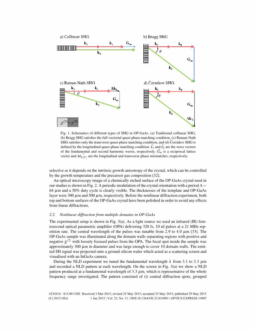
Fig. 1. Schematics of different types of SHG in OP-GaAs. (a) Traditional collinear SHG,(b) Bragg SHG satisfies the full vectorial quasi-phase matching condition, (c) Raman-NathSHG satisfies only the transverse quasi-phase matching condition, and (d) Cerenkov SHG isdefined by the longitudinal quasi-phase matching condition. ~k1 and ~k2 are the wave vectorsof the fundamental and second harmonic waves, respectively, ~Gm is a reciprocal latticevector and ∆ ~kL(T ) are the longitudinal and transverse phase mismatches, respectively.
selective as it depends on the intrinsic growth anisotropy of the crystal, which can be controlledby the growth temperature and the precursor gas composition [32].
An optical microscopy image of a chemically etched surface of the OP-GaAs crystal used inour studies is shown in Fig. 2. A periodic modulation of the crystal orientation with a period Λ=64 µm and a 50% duty cycle is clearly visible. The thicknesses of the template and OP-GaAslayer were 300 µm and 500 µm, respectively. Before the nonlinear diffraction experiment, bothtop and bottom surfaces of the OP-GaAs crystal have been polished in order to avoid any effectsfrom linear diffractions.
2.2. Nonlinear diffraction from multiple domains in OP-GaAs
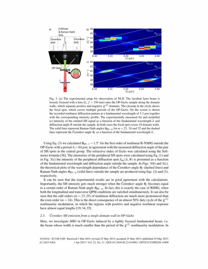
The experimental setup is shown in Fig. 3(a). As a light source we used an infrared (IR) fem-tosecond optical parametric amplifier (OPA) delivering 320 fs, 10 nJ pulses at a 21 MHz rep-etition rate. The central wavelength of the pulses was tunable from 2.9 to 4.0 µm [33]. TheOP-GaAs sample was illuminated along the domain walls separating regions with positive andnegative χ(2) with loosely focused pulses from the OPA. The focal spot inside the sample wasapproximately 300 µm in diameter and was large enough to cover 10 domain walls. The emit-ted SH signal was projected onto a ground silicon wafer which acted as a scattering screen andvisualised with an InGaAs camera.
During the NLD experiment we tuned the fundamental wavelength λ from 3.1 to 3.3 µmand recorded a NLD pattern at each wavelength. On the screen in Fig. 3(a) we show a NLDpattern produced at a fundamental wavelength of 3.3 µm, which is representative of the wholefrequency range investigated. The pattern consisted of (i) central diffraction spots, grouped
#234416 - $15.00 USD Received 3 Mar 2015; revised 25 May 2015; accepted 25 May 2015; published 29 May 2015 (C) 2015 OSA 1 Jun 2015 | Vol. 23, No. 11 | DOI:10.1364/OE.23.014903 | OPTICS EXPRESS 14907

Z [001]
X [-110]
[00-1] domain [001] domain
100 µm
Fig. 2. Cross-sections of a 500 µm thick GaAs film grown on a OP-GaAs template ofperiod Λ = 64 µm.
around the fundamental beam position, and (ii) peripheral diffraction spots, located relativelyfar away from the central spots on both sides of the diffraction pattern (left and right spots onthe screen in Fig. 3(a)). The central diffraction spots included a collinear SH spot, which wasobservable only when the fundamental wave was focused at the OP-GaAs surface, and a pairof NLD spots, which were symmetric with respect to the collinear spot. The measured externaldiffraction angle of the two NLD spots was ±1.5◦. Figure 3(b) shows the normalised intensityof the peripheral NLD spots as a function of the fundamental wavelength λ and diffractionangle θ .
To explain the NLD pattern, we consider the intensity of SHG from a periodic χ(2) structure,which can be written as [34, 35]:
I2ω ∼ I2ω ×S2
L ×S2T , (1)
where Iω is the intensity of the fundamental beam inside the material and SL(T ) are functionsdescribing the longitudinal and transverse QPM conditions, respectively. The longitudinal QPMcondition is satisfied when the function SL = sinc
[z((k2 cosθ)2 − (2k1)
2)/2]
approaches itsmaximum. In the above expressions, sinc(x) = sin(x)/x and z is the interaction length. TheSHG angle inside the sample satisfying this QPM condition is the Cerenkov angle θC:
θC = cos−1 n1
n2, (2)
where n1 and n2 are the refractive indices of the medium at the fundamental and SH wave-lengths, respectively.
As in the previous case, the transverse QPM condition is defined by the maximum of thefunction ST = ∑
m=0,±1,±2,...gme−w2(k2 sinθ+Gm)
2/8, where w is the width of the fundamental beam
and gm are Fourier coefficients, which depend on the duty cycle of the χ(2) nonlinear grat-ing [34, 35]. The transverse QPM condition defines Raman-Nath angles θRN, m inside the sam-ple:
θRN, m = sin−1 mλ
2n2Λ. (3)
#234416 - $15.00 USD Received 3 Mar 2015; revised 25 May 2015; accepted 25 May 2015; published 29 May 2015 (C) 2015 OSA 1 Jun 2015 | Vol. 23, No. 11 | DOI:10.1364/OE.23.014903 | OPTICS EXPRESS 14908
b)
c)
38
39
40
41
42
43
38
39
40
41
42
43
3.10 3.15 3.20 3.25 3.30
3.10 3.15 3.20 3.25 3.30
λ [ μm ]
λ [ μm ]
θ [
° ]
θ [
° ]
θC
θRN, 25
θRN, 24
θRN, 23
θC
θRN, 25
θRN, 24
θRN, 23
OP-GaAs
L
Collinear & Raman-Nath SHG
Čerenkov SHG
Čerenkov SHG
a)
Fig. 3. (a) The experimental setup for observation of NLD. The incident laser beam isloosely focused with a lens (L, f = 150 mm) onto the OP-GaAs sample along the domainwalls, which separate positive and negative χ(2) domains. The closeup in the circle showsthe focal spot, which covers multiple periods of the OP-GaAs. On the screen is shownthe recorded nonlinear diffraction pattern at a fundamental wavelength of 3.3 µm togetherwith the corresponding intensity profile. The experimentally measured (b) and modelled(c) intensity of the emitted SH signal as a function of the fundamental wavelength λ anddiffraction angle θ outside the sample. In both cases the focal spot covers 10 domain walls.The solid lines represent Raman-Nath angles θRN, m for m = 23, 24 and 25 and the dashedlines represent the Cerenkov angle θC as a function of the fundamental wavelength λ .
Using Eq. (3) we calculated θRN, 1 = 1.5◦ for the first order of nonlinear R-NSHG outside theOP-GaAs with a period Λ= 64 µm, in agreement with the measured diffraction angle of the pairof SH spots in the central group. The refractive index of GaAs was calculated using the Sell-meier formula [36]. The intensities of the peripheral SH spots were calculated using Eq. (1) andin Fig. 3(c) the intensity of the peripheral diffraction spot I2ω (λ ,θ) is presented as a functionof the fundamental wavelength and diffraction angle outside the sample. In Figs. 3(b) and 3(c),the theoretical plots of the wavelength dependance of the Cerenkov angle θC (dashed lines) andRaman-Nath angles θRN, m (solid lines) outside the sample are produced using Eqs. (2) and (3),respectively.
It can be seen that the experimental results are in good agreement with the calculations.Importantly, the SH intensity gets much stronger when the Cerenkov angle θC becomes equalto a certain order of Raman-Nath angle θRN, m. In fact, this is exactly the case of BSHG, whenboth the longitudinal and transverse QPM conditions are satisfied simultaneously. It can also beseen that the odd orders (m = 23,25) of nonlinear diffraction are much more pronounced thanthe even order (m = 24). This is the direct consequence of an almost 50% duty cycle of the χ(2)
nonlinearity modulation, in which the regions with positive and negative nonlinear responsehave almost equal lengths [19, 34, 35].
2.3. Cerenkov SH emission from a single domain wall in OP-GaAs
Here, we investigate SHG in OP-GaAs induced by a tightly focused fundamental beam, i.e.the beam whose width is much smaller than the period of the χ(2) nonlinearity modulation. In
#234416 - $15.00 USD Received 3 Mar 2015; revised 25 May 2015; accepted 25 May 2015; published 29 May 2015 (C) 2015 OSA 1 Jun 2015 | Vol. 23, No. 11 | DOI:10.1364/OE.23.014903 | OPTICS EXPRESS 14909

this situation, the fundamental beam illuminates either a homogeneous region of the sampleor the wall separating oppositely oriented domains. As we have shown recently [37], in thisgeometry only the Cerenkov SH signal is generated, which occurs when the fundamental beamilluminates a domain wall. No R-NSHG can be observed as it requires the participation ofmultiple grating periods.
The experimental setup is shown in Fig. 4(a). The sample was mounted on a XYZ-translationstage and could be scanned with a 60 nm resolution. We used the same OPA source as inSection 2.2. The fundamental beam (λ = 3.5 µm) was chopped at 1 kHz and focused insidethe sample using a molded chalcogenide lens with an effective NA = 0.3. The SH signal wascollected with an IR-corrected objective with NA = 0.65. A spatial filter was used to block thesurface-induced collinear SHG to ensure that only the Cerenkov SH signal was focused ontothe InGaAs photodiode and processed using a lock-in amplifier.
0 100 200 300 400 500 6000.0
0.5
1.0
CS
HG
[ a
.u.
]
Z [ m ]
0.0 0.5 1.0
0
30
60
90
120
CSHG [ a.u. ]
X [
m ]
d)
X
Z
b)
c) a) Ph
OP-GaAs
Ch
Ob1
Ob2
F
Fig. 4. (a) The experimental setup for observation of CSHG using a tightly focused fun-damental beam: Ch - chopper, Ob1 - NA = 0.3 objective, Ob2 - NA = 0.65 objective, F -spatial filter, Ph - InGaAs photodiode. The inset shows the focusing configuration insidethe OP-GaAs: the focal spot is much smaller than the period of the χ(2) nonlinearity modu-lation. (b) The intensity of the emitted Cerenkov signal recorded by translating the samplein the XZ plane. (c) and (d) show the Cerenkov intensity profiles along the X and Z axes,respectively.
In this configuration we measured the CSHG intensity as a function of the focal spot positioninside the sample. Scanning at a constant velocity proceeded first along the X direction. Thelock-in signal from the detector was triggered by the stage controller to synchronise the dataacquisition process with the motion of the stage. In this way, we could achieve a 0.5 µm resolu-tion along the X axis. Scans along the Y and Z axes were performed at 2 and 20 µm resolution,respectively.
The resolution of the domain wall image is determined by both the resolution of the scanningsystem and the size of the OPA focus inside the sample. The focal radius w0 of an incomingfundamental beam with a Gaussian intensity profile is given by w0 = λ/πNA and in our caseis estimated at 3.7 µm in the lateral, i.e. XY, plane. In the longitudinal, i.e. Z, direction the sizeof the focus is determined by the Rayleigh length zR = (πn1w2
0)/λ ≈ 41 µm. In addition, theresolution is also affected by spherical aberration caused by the high refractive index mismatchbetween the ambient air and the GaAs sample at both the fundamental and SH wavelengths.
Figure 4(b) shows a two-dimensional intensity pattern of the Cerenkov SH signal in the XZplane. The colour change from blue to red reflects variation of the Cerenkov SH intensity fromlow to high. It can be seen that CSHG is very sensitive to the position of the focal spot with
#234416 - $15.00 USD Received 3 Mar 2015; revised 25 May 2015; accepted 25 May 2015; published 29 May 2015 (C) 2015 OSA 1 Jun 2015 | Vol. 23, No. 11 | DOI:10.1364/OE.23.014903 | OPTICS EXPRESS 14910

respect to the domain walls. The maxima of the SH signal coincide with the locations of thedomain walls in the OP-GaAs sample.
In Fig. 4(c), we plot a typical CSHG intensity profile along the X axis. The separation be-tween the maxima is 32 µm, which is half of the χ(2) nonlinearity modulation period Λ. Thisresult confirms the 50% duty cycle. Figure 4(d) displays the CSHG intensity profile in the wholescanned region along the Z direction. One can see that the strength of the CSHG remains almostconstant inside the sample and decreases gradually at the ends of the sample. This is becausethe effective interaction length decreases when the focus of the fundamental beam moves outof the sample.
2.4. Three-dimensional visualisation of orientation-patterned GaAs
The sensitivity of CSHG to the presence of domain walls can be used to provide a contrast inscanning microscopy to visualise the domain structure of OP-GaAs in 3D. It should be stressedthat, the demonstrated CSHG-based scanning microscopy technique is totally non-destructiveas it does not require any cutting or etching to reveal the bulk domain structure. In Fig. 5,we present a 3D image of the domain pattern inside the OP-GaAs sample. The image wascreated by stacking a number of XY scans recorded at different depths Z. The box in the Fig. 5represents the whole scanning volume 200x200x600 µm3. It is clear that our CSHG-basedmicroscopy technique allows us to not only reveal the nonlinear grating parameters such as theperiod and duty cycle, but also to determine the quality of orientation patterning in the bulk of asample. For example, in Fig. 5 we show that the domain structure is nonuniform in the scannedregion. In particular, the effect of merging of two neighbouring domains, which were initiallyseparated, is evident.
X
Y Z
Fig. 5. A three-dimensional image of the OP-GaAs structure, obtained by scanning the fun-damental beam inside the sample and recording the strength of the corresponding nonlinearCerenkov diffraction at each position. The size of the box is 200x200x600 µm3.
3. Conclusions
We have presented the nonlinear diffraction in a OP-GaAs crystal. In particular, we have shownnonlinear Raman-Nath and Cerenkov second harmonic emission from a periodically modulated
#234416 - $15.00 USD Received 3 Mar 2015; revised 25 May 2015; accepted 25 May 2015; published 29 May 2015 (C) 2015 OSA 1 Jun 2015 | Vol. 23, No. 11 | DOI:10.1364/OE.23.014903 | OPTICS EXPRESS 14911

χ(2) nonlinearity. We explain this effect by employing the concepts of longitudinal and trans-verse quasi-phase matching and show that the intensity of nonlinear diffraction is maximum,i.e. Bragg second harmonic generation, when these two conditions are satisfied simultaneously.
We have also shown that Cerenkov second harmonic emission in the sample can be usedto visualise the 3D structure of the χ(2) nonlinearity modulation. Unlike traditional character-isation methods based on scanning electron microscopy or optical microscopy, which requirecutting, polishing and etching of the samples, our technique is nondestructive and enables oneto visualise the QPM structure everywhere in the bulk of the sample. This constitutes a uniquenondestructive diagnostic tool for characterisation of orientation-patterned semiconductors and,potentially, any variations of the second-order nonlinearities in semiconducting materials.
Acknowledgments
The authors thank the Australian Research Council for financial support. P. Karpinski thanksthe Polish Ministry of Science and Higher Education for ”Mobility Plus” scholarship.
#234416 - $15.00 USD Received 3 Mar 2015; revised 25 May 2015; accepted 25 May 2015; published 29 May 2015 (C) 2015 OSA 1 Jun 2015 | Vol. 23, No. 11 | DOI:10.1364/OE.23.014903 | OPTICS EXPRESS 14912