Non-Volatile Memory Technologiescs7810/pres/nvram-cs7810x2.pdfNon-Volatile Memory Technologies A...
33
P a g e ‹ # › 1 CS7810 School of Computing University of Utah Non-Volatile Memory Technologies A Survey 2 CS7810 School of Computing University of Utah Generic Taxonomy: V & NV • Volatile SRAM - 5 or 6 transistors per cell » fast but costly & power hungry » usage • on chip - caches, register files, buffers, queues, etc. • off chip usage now rare except in embedded space DRAM - 1 T & 1 C per cell (lots of details later in the term) » focus on density and cost/bit • too bad both power and delay properties are problematic » usage - main memory • EDRAM now moving on chip for large “last cache” duties » specialty parts for mobile systems • low-power • self-refresh • takes advantage of light usage » battery backed DRAM - common in data-center
Transcript of Non-Volatile Memory Technologiescs7810/pres/nvram-cs7810x2.pdfNon-Volatile Memory Technologies A...

P a g e ‹ # ›
1 CS7810School of ComputingUniversity of Utah
Non-VolatileMemory Technologies
A Survey
2 CS7810School of ComputingUniversity of Utah
Generic Taxonomy: V & NV• Volatile
SRAM - 5 or 6 transistors per cell» fast but costly & power hungry» usage
• on chip - caches, register files, buffers, queues, etc.• off chip usage now rare except in embedded space
DRAM - 1 T & 1 C per cell (lots of details later in the term)» focus on density and cost/bit
• too bad both power and delay properties are problematic
» usage - main memory• EDRAM now moving on chip for large “last cache” duties
» specialty parts for mobile systems• low-power• self-refresh• takes advantage of light usage
» battery backed DRAM - common in data-center

P a g e ‹ # ›
3 CS7810School of ComputingUniversity of Utah
NV• Traditional non-volatile
Magnetic Disk» cheap» mixed use: file system and scratch
CD, DVD» even cheaper per unit but less capacity» media and SW distribution, personal archival
Tape» cheapest» archival storage
Solid state» more spendy but faster
• PROM in various flavors - now primarily masked on chip• FLASH has essentially taken over at the component level• new contenders are on the horizon however
4 CS7810School of ComputingUniversity of Utah
Problems Everywhere• 1945
Von Neumann’s classic paper Conclusion: memory is the bottleneck
» vacuum tube technology at the time Note: his conclusion has been persistently correct
• Now ITRS
» pin count and pin bandwidth won’t go up much• signal integrity, cost, and power constraints
Multi-core» core count predicted to go up at Moore’s rate» lots of compute but with little increase in memory bandwidth
• looks like a train wreck is in our future• significant industry momentum - similar to a train

P a g e ‹ # ›
5 CS7810School of ComputingUniversity of Utah
Some Observations• Bandwidth and Latency
both are important» latency problems can be hidden to some extent» bandwidth problems are much harder to hide
• Increasing the storage hierarchy depth conventional approach
» big memories are slow» helps with fragmentation & BW issues
• Yale vs. Harvard
conflicts with power constraints now» moving lots of bits over long wires is energy expensive
• Somewhat troubling how little mem_arch has changed in 60 years opportunity
6 CS7810School of ComputingUniversity of Utah
The Changing Landscape• Disruptive technologies
SSD’s are on the market now» better in terms of performance» much worse in terms of cost/bit
• hard to see a future where FLASH wins this race» longevity - open question
all technologies have a life-span: tubes, core, transistors, …
• New roles lots of cores, parallelism, and flakey components
» manufacturing and operational variation back up often and checkpoint
» NVRAM needed - checkpoints shouldn’t be volatile• ideal use = write-only• low energy fast writes - reads can be more expensive
– inversion of the normal viewpoint
multiple special memories - e.g. texture cache in GPU land
P a g e ‹ # ›
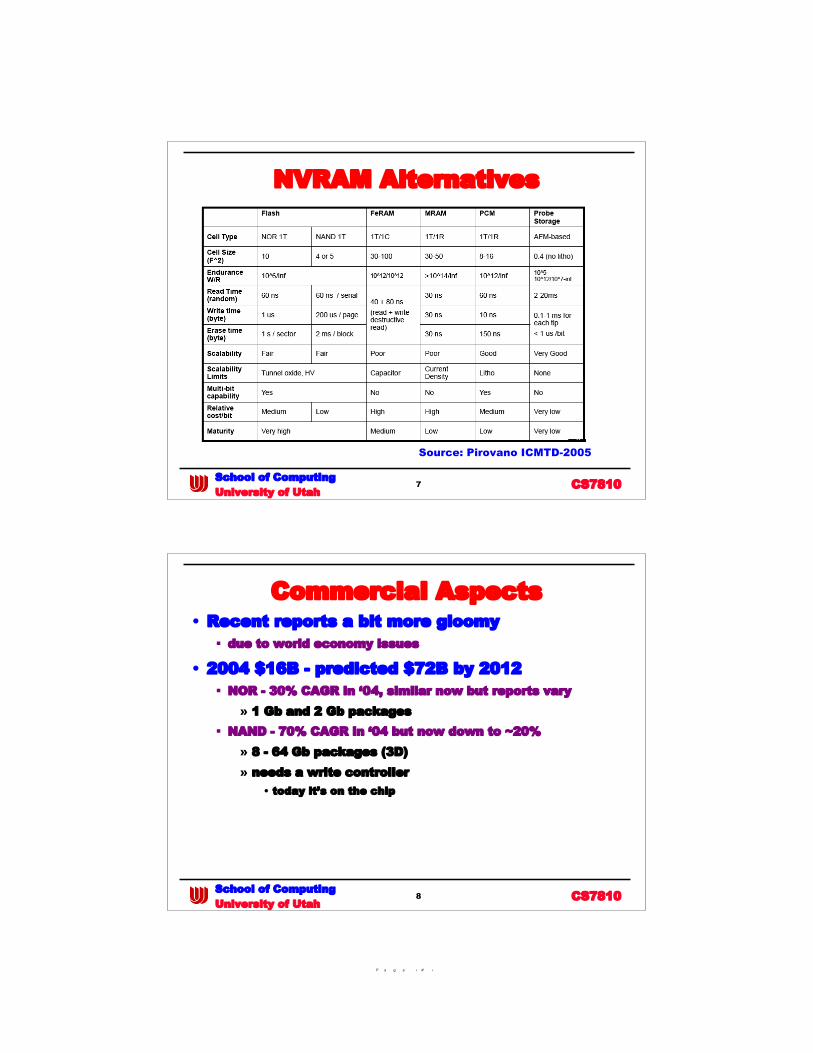
7 CS7810School of ComputingUniversity of Utah
NVRAM Alternatives
Source: Pirovano ICMTD-2005
8 CS7810School of ComputingUniversity of Utah
Commercial Aspects• Recent reports a bit more gloomy
due to world economy issues
• 2004 $16B - predicted $72B by 2012 NOR - 30% CAGR in ‘04, similar now but reports vary
» 1 Gb and 2 Gb packages NAND - 70% CAGR in ‘04 but now down to ~20%
» 8 - 64 Gb packages (3D)» needs a write controller
• today it’s on the chip
P a g e ‹ # ›
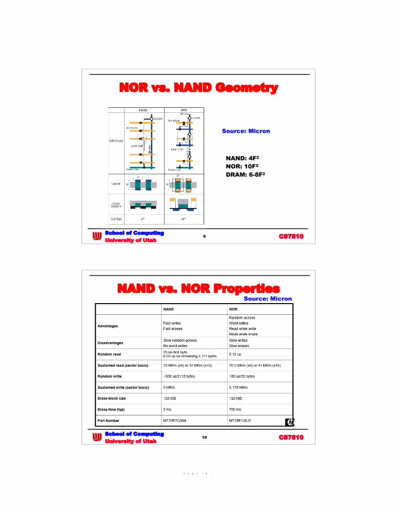
9 CS7810School of ComputingUniversity of Utah
NOR vs. NAND Geometry
Source: Micron
NAND: 4F2
NOR: 10F2
DRAM: 6-8F2
10 CS7810School of ComputingUniversity of Utah
NAND vs. NOR PropertiesSource: Micron
P a g e ‹ # ›
11 CS7810School of ComputingUniversity of Utah
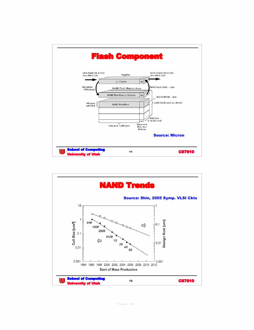
Flash Component
Source: Micron
12 CS7810School of ComputingUniversity of Utah
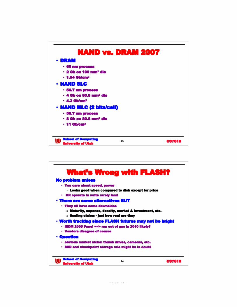
NAND TrendsSource: Shin, 2005 Symp. VLSI Ckts
P a g e ‹ # ›
13 CS7810School of ComputingUniversity of Utah
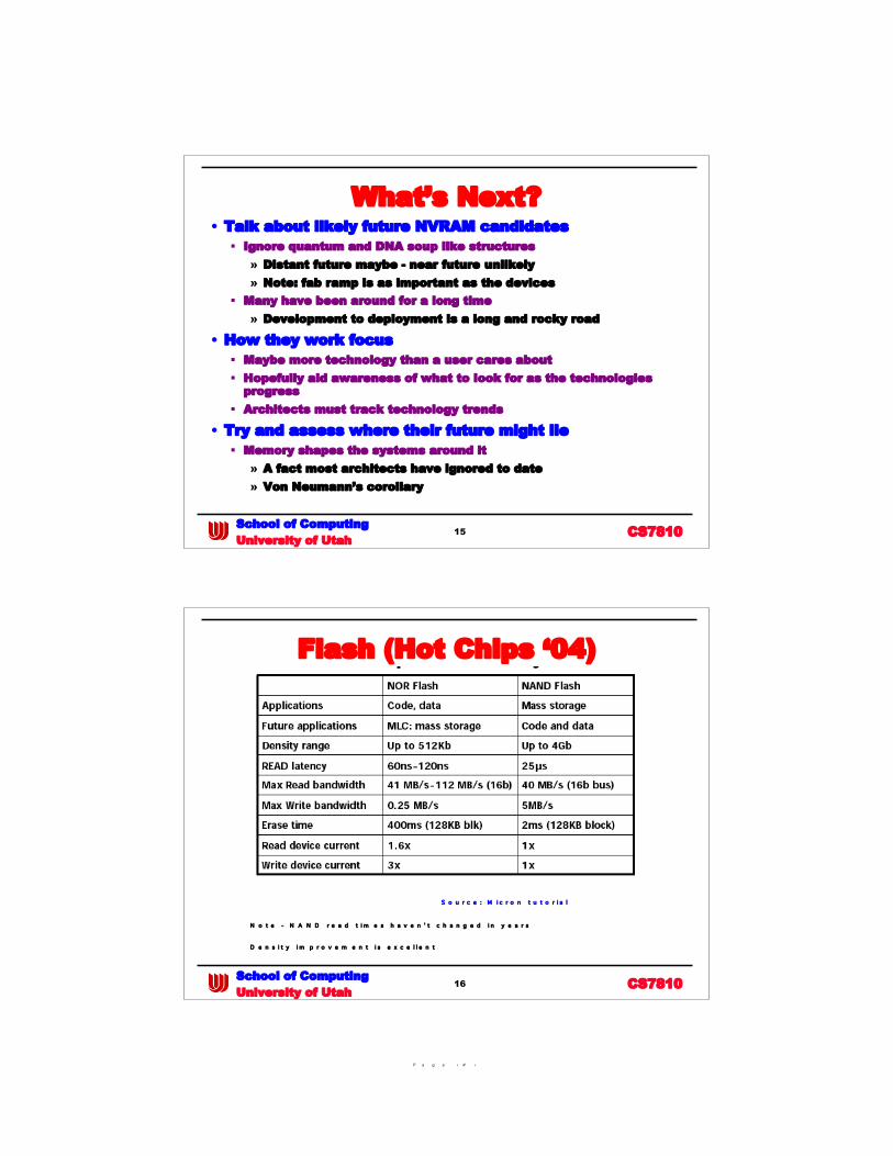
NAND vs. DRAM 2007• DRAM
65 nm process 2 Gb on 100 mm2 die 1.94 Gb/cm2
• NAND SLC 56.7 nm process 4 Gb on 80.8 mm2 die 4.3 Gb/cm2
• NAND MLC (2 bits/cell) 56.7 nm process 8 Gb on 80.8 mm2 die 11 Gb/cm2
14 CS7810School of ComputingUniversity of Utah
What’s Wrong with FLASH?No problem unless
You care about speed, power» Looks good when compared to disk except for price
OR operate in write rarely land
• There are some alternatives BUT They all have some downsides
» Maturity, expense, density, market & investment, etc.» Scaling claims - just how real are they
• Worth tracking since FLASH futures may not be bright IEDM 2005 Panel ==> run out of gas in 2010 likely? Vendors disagree of course
• Question obvious market niche: thumb drives, cameras, etc. SSD and checkpoint storage role might be in doubt
P a g e ‹ # ›
15 CS7810School of ComputingUniversity of Utah
What’s Next?• Talk about likely future NVRAM candidates
Ignore quantum and DNA soup like structures» Distant future maybe - near future unlikely» Note: fab ramp is as important as the devices
Many have been around for a long time» Development to deployment is a long and rocky road
• How they work focus Maybe more technology than a user cares about Hopefully aid awareness of what to look for as the technologies
progress Architects must track technology trends
• Try and assess where their future might lie Memory shapes the systems around it
» A fact most architects have ignored to date» Von Neumann’s corollary
16 CS7810School of ComputingUniversity of Utah
Flash (Hot Chips ‘04)
N o t e - N A N D r e a d t i m e s h a v e n ’ t c h a n g e d i n y e a r s
D e n s i t y i m p r o v e m e n t i s e x c e l l e n t
S o u r c e : M i c r o n t u t o r i a l

P a g e ‹ # ›
17 CS7810School of ComputingUniversity of Utah
Known FLASH issues• Speed - slow writes OK, but 25 usec reads??
High voltage on both read and write create problems» Charge pump takes time» Jitter on bit lines requires lengthy settle margin
Conclusion is that reads are unlikely to get much faster
• Retention Thicker tunnel oxide (7-12nm) provides good retention, but
» High voltage requirements create reliability issue.• Channel punch through, junction breakdown, etc.• Also increases the read and write energies
• Scaling Concern over single defect memory loss limits vertical scaling High voltage also limits lateral scaling to some extent Rad hard arrays are difficult to achieve Support circuitry doesn’t scale as well as the arrays
18 CS7810School of ComputingUniversity of Utah
More Issues• Retention
106 block erase wear out» Gets considerably worse for multi-bit cells
Density/Retention trade-off Wear leveling a must for computer systems
» Who cares for iPods, cameras, etc.
• Use model Somewhat goofy
» Write once cells or block erase» Complex controller
Not much worse than DRAM however

P a g e ‹ # ›
19 CS7810School of ComputingUniversity of Utah
SONOS/MONOS• ONOS - oxide nitride oxide semiconductor
M=metal gate - common outside US S= silicon - more common in US
• Varying views Some view as a FLASH evolution Others view as a fundamentally different technology Both views are credible but who cares
20 CS7810School of ComputingUniversity of Utah
Why should we be interested• Relatively mature
Already in production» SONY is basing their SoC strategy on this» TSMC, Grumman, Hitachi, Philips & Toshiba also have
the process» Compatible with CMOS fab
Density» 6F2 cell (same as DRAM)
Lower than FLASH program voltage 5-8V Scales better
» Working @ 20 nm, 1ms program and erase» Reported IEDM ‘05 by TSMC (J. R. Hwang et al)
P a g e ‹ # ›
21 CS7810School of ComputingUniversity of Utah
Not a new technology• Current usage
Satellite and space craft» Inherently rad-hard
• important at small size & enables cheap packaging
• Why haven’t we seen it Concerns about data retention Density not as good as FLASH
• What’s changed 2 bit per cell ==> density better than FLASH
» Possible for FLASH too but much harder to control Retention now at 10 years after 107 write/erase
» Primarily due to anneal w/ deuterium rather than hydrogen» Promise of hi-K dielectrics - viz. HfO & HfO2
22 CS7810School of ComputingUniversity of Utah
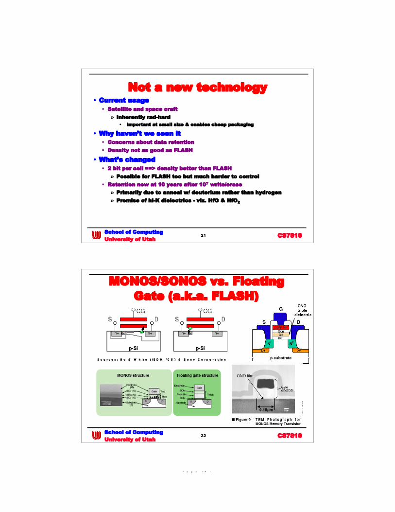
MONOS/SONOS vs. FloatingGate (a.k.a. FLASH)
S o u r c e s : B u & W h i t e ( I E D M ‘ 0 5 ) & S o n y C o r p o r a t i o n
P a g e ‹ # ›
23 CS7810School of ComputingUniversity of Utah
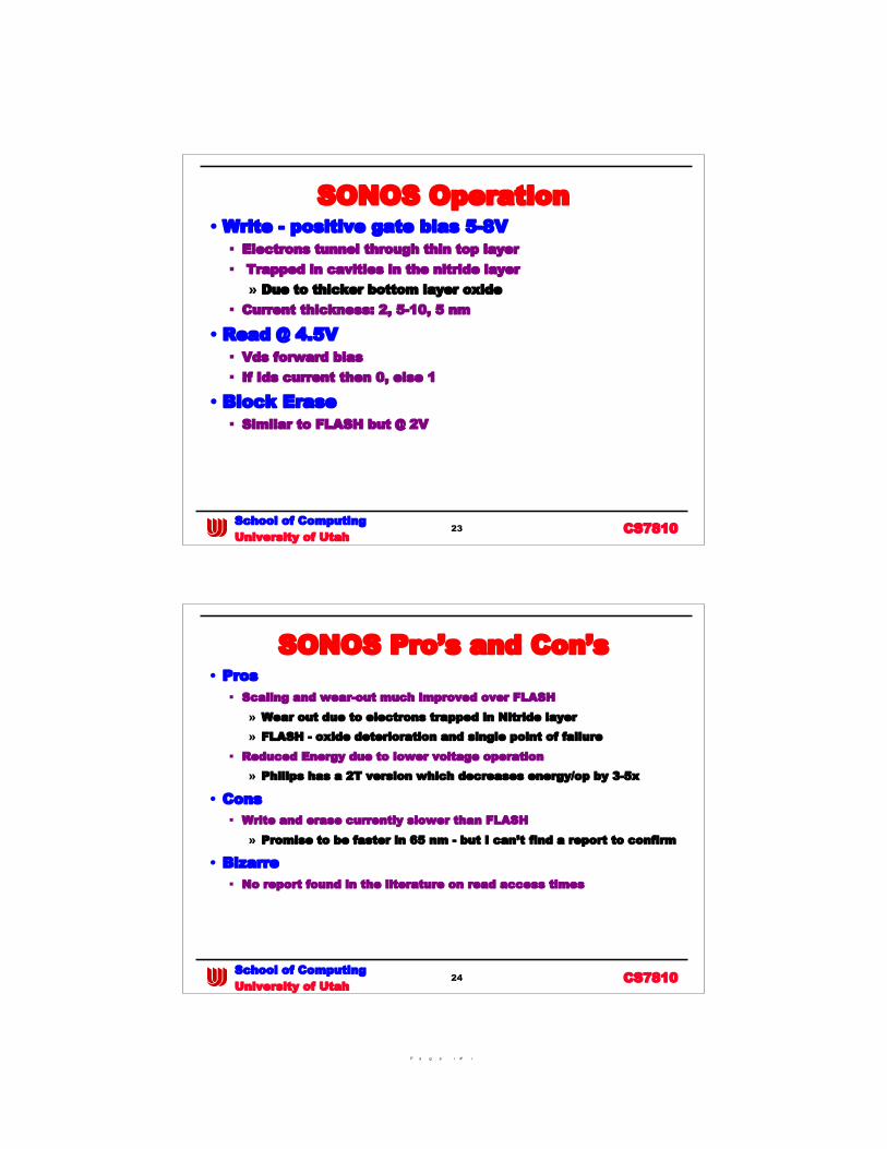
SONOS Operation• Write - positive gate bias 5-8V
Electrons tunnel through thin top layer Trapped in cavities in the nitride layer
» Due to thicker bottom layer oxide Current thickness: 2, 5-10, 5 nm
• Read @ 4.5V Vds forward bias If Ids current then 0, else 1
• Block Erase Similar to FLASH but @ 2V
24 CS7810School of ComputingUniversity of Utah
SONOS Pro’s and Con’s• Pros
Scaling and wear-out much improved over FLASH» Wear out due to electrons trapped in Nitride layer» FLASH - oxide deterioration and single point of failure
Reduced Energy due to lower voltage operation» Philips has a 2T version which decreases energy/op by 3-5x
• Cons Write and erase currently slower than FLASH
» Promise to be faster in 65 nm - but I can’t find a report to confirm
• Bizarre No report found in the literature on read access times

P a g e ‹ # ›
25 CS7810School of ComputingUniversity of Utah
Phase Change RAM• Tower of Babel naming
PCRAM, PRAM, PCM, OUM, CRAM
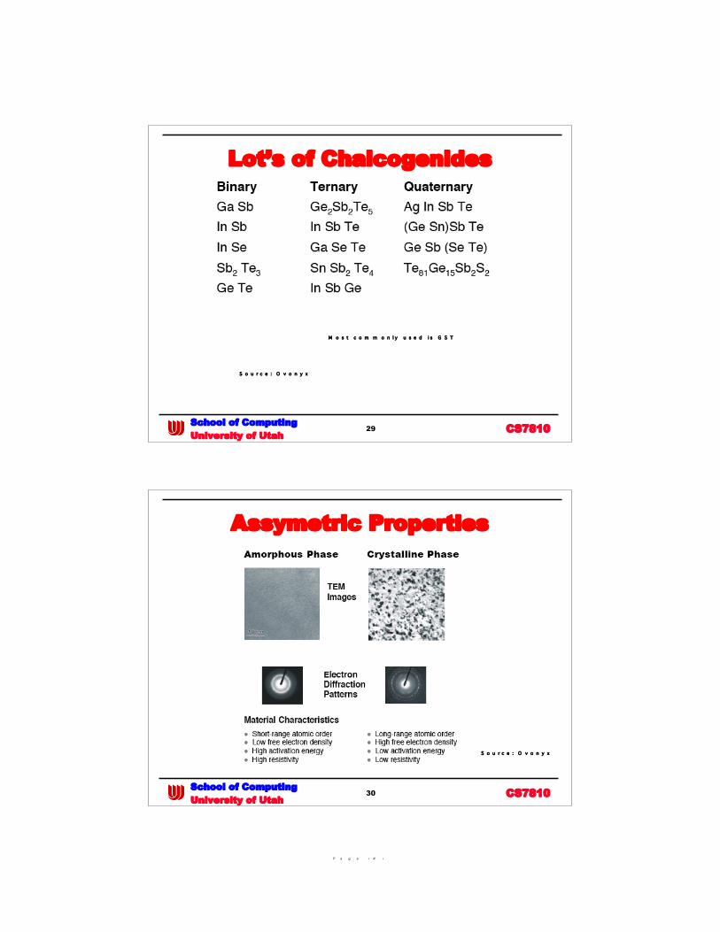
• Basis Chalcogenide material
» 2 states - crystalline and amorphous• Actually lots of states in between
» 0 = Amorphous - quench after heating to > 619 C• High resistive, high refractive index
» 1 = Crystalline - heat > 223 C• Low resistive, low refractive index
» Quench must cool to < 100 C NOTE
» Properties and temps vary slightly w/ specific material
26 CS7810School of ComputingUniversity of Utah
Also Not a New Technology• Timeline
‘66 Stanford Ovshinsky (ECD) first patent ‘69 ECD patent and working device ‘99 Ovonyx joint venture starts as license source ‘04 64 Mb Samsung part ‘05 256 Mb Samsung plus w/ 100 uA programming
» Hitachi 100 uA @ 1.5v programming current ‘06 BAE puts rad-hard parts in space
» 1st commercially available part ‘06 STM 128 Mb commercial ‘07 IDF demo by Justin Rattner of Intel version

P a g e ‹ # ›
27 CS7810School of ComputingUniversity of Utah
We use this stuff now -differently
• CD-RW and DVD-RW Chalcogenide based Laser to do the heating Read based on refraction differences - not resistance
28 CS7810School of ComputingUniversity of Utah
Basic Device
P a g e ‹ # ›
29 CS7810School of ComputingUniversity of Utah
Lot’s of Chalcogenides
M o s t c o m m o n l y u s e d i s G S T
S o u r c e : O v o n y x
30 CS7810School of ComputingUniversity of Utah
Assymetric Properties
S o u r c e : O v o n y x
P a g e ‹ # ›
31 CS7810School of ComputingUniversity of Utah
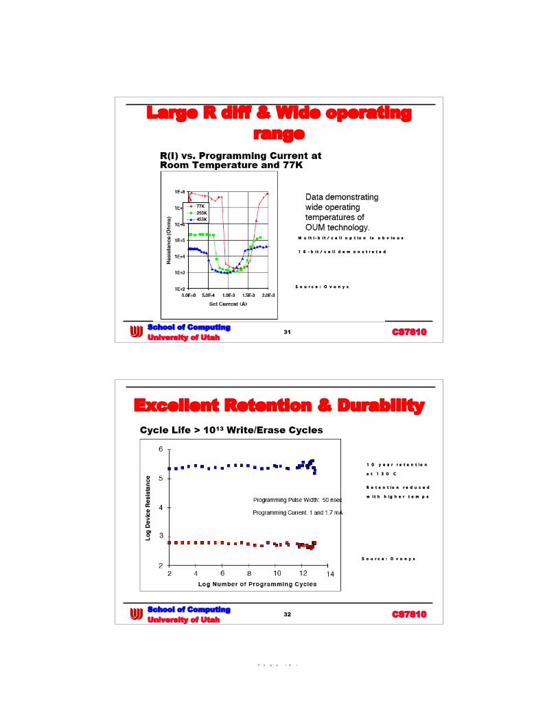
Large R diff & Wide operatingrange
M u l t i - b i t / c e l l o p t i o n i s o b v i o u s
1 6 - b i t / c e l l d e m o n s t r a t e d
S o u r c e : O v o n y x
32 CS7810School of ComputingUniversity of Utah
Excellent Retention & Durability
S o u r c e : O v o n y x
1 0 y e a r r e t e n t i o n
a t 1 3 0 C
R e t e n t i o n r e d u c e d
w i t h h i g h e r t e m p s

P a g e ‹ # ›
33 CS7810School of ComputingUniversity of Utah
Multi-bit requires Multi-pulse
E a s i e r c o n t r o l r e g i m e
t h a n a s i n g l e p u l s e w /
v a r y i n g d u r a t i o n
S o u r c e : O v o n y x
34 CS7810School of ComputingUniversity of Utah
Basically a very cheap material
S o u r c e : O v o n y x
P a g e ‹ # ›
35 CS7810School of ComputingUniversity of Utah
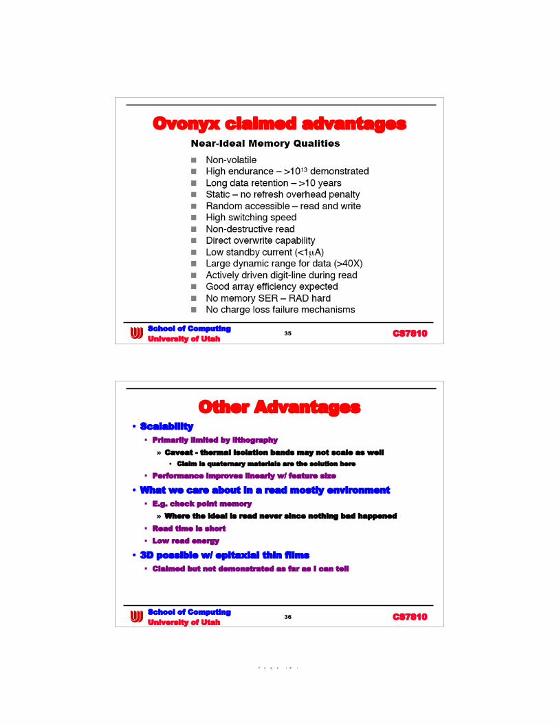
Ovonyx claimed advantages
36 CS7810School of ComputingUniversity of Utah
Other Advantages• Scalability
Primarily limited by lithography» Caveat - thermal isolation bands may not scale as well
• Claim is quaternary materials are the solution here
Performance improves linearly w/ feature size
• What we care about in a read mostly environment E.g. check point memory
» Where the ideal is read never since nothing bad happened Read time is short Low read energy
• 3D possible w/ epitaxial thin films Claimed but not demonstrated as far as I can tell
P a g e ‹ # ›
37 CS7810School of ComputingUniversity of Utah
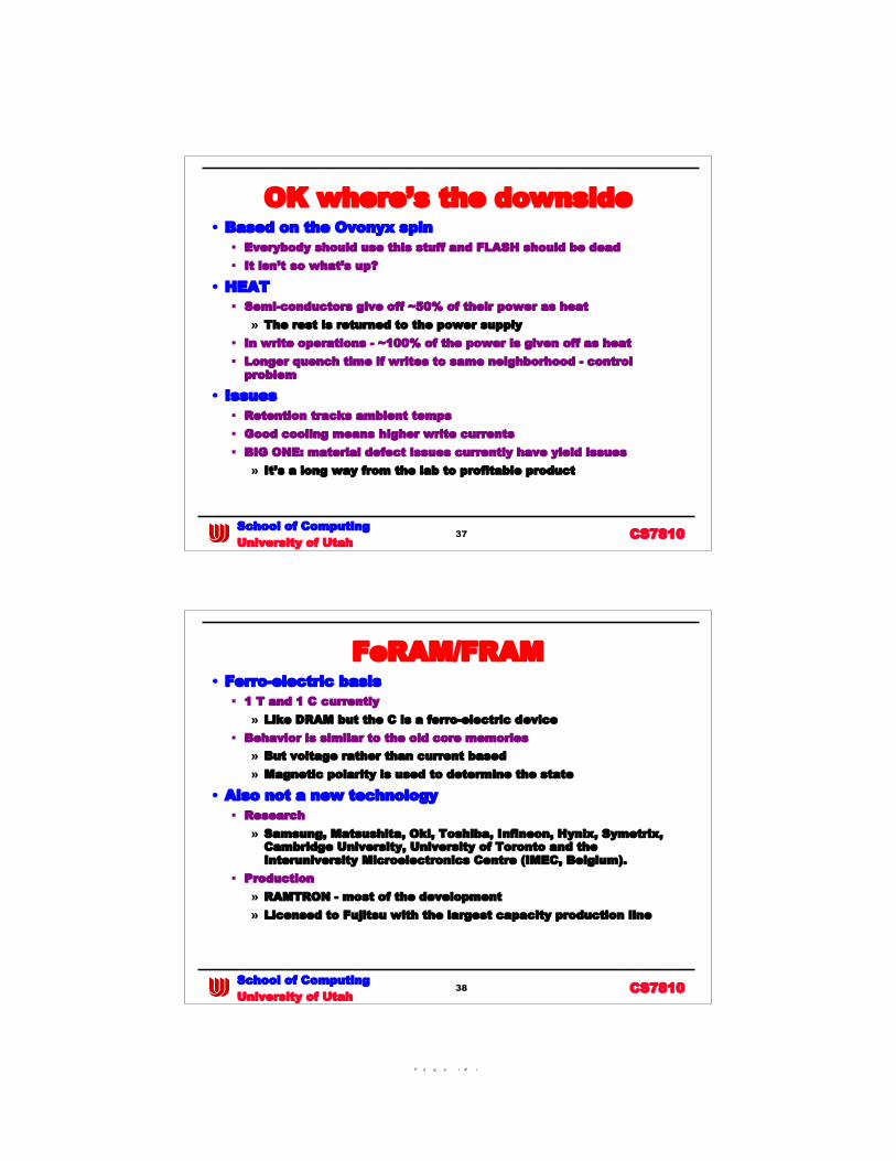
OK where’s the downside• Based on the Ovonyx spin
Everybody should use this stuff and FLASH should be dead It isn’t so what’s up?
• HEAT Semi-conductors give off ~50% of their power as heat
» The rest is returned to the power supply In write operations - ~100% of the power is given off as heat Longer quench time if writes to same neighborhood - control
problem
• Issues Retention tracks ambient temps Good cooling means higher write currents BIG ONE: material defect issues currently have yield issues
» It’s a long way from the lab to profitable product
38 CS7810School of ComputingUniversity of Utah
FeRAM/FRAM• Ferro-electric basis
1 T and 1 C currently» Like DRAM but the C is a ferro-electric device
Behavior is similar to the old core memories» But voltage rather than current based» Magnetic polarity is used to determine the state
• Also not a new technology Research
» Samsung, Matsushita, Oki, Toshiba, Infineon, Hynix, Symetrix,Cambridge University, University of Toronto and theInteruniversity Microelectronics Centre (IMEC, Belgium).
Production» RAMTRON - most of the development» Licensed to Fujitsu with the largest capacity production line

P a g e ‹ # ›
39 CS7810School of ComputingUniversity of Utah
Dwarfed by FLASH• Gartner Group 2005 reports
18.6 B$ FLASH 23 M$ for Ramtron
» Probably the largest supplier (made by Fujitsu??)
• Promise (conflicting reports) When compared to FLASH FeRAM offers
» lower power» faster write speed» much greater maximum number (exceeding 1016 for 3.3
V devices) of write-erase cycles.
40 CS7810School of ComputingUniversity of Utah
FeRAM Device Basics
B a s i c P l a n a r D e s i g n
S m a l l e r S t a c k e d V i a V a r i a n t
S o u r c e : P r o c I E E E , V . 8 8 , N o . 5 , M a y 2 0 0 0
L o o k s a l o t l i k e D R A M u s i n g p l a n a r C ’ s
P a g e ‹ # ›
41 CS7810School of ComputingUniversity of Utah
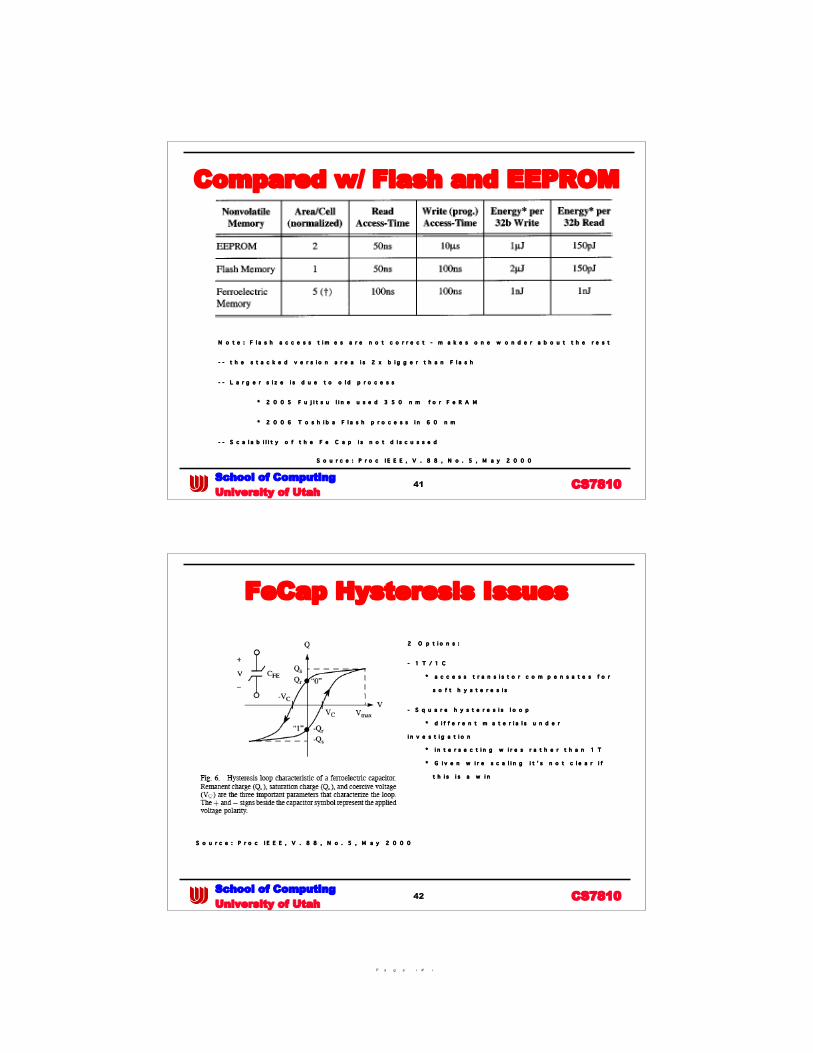
Compared w/ Flash and EEPROM
N o t e : F l a s h a c c e s s t i m e s a r e n o t c o r r e c t - m a k e s o n e w o n d e r a b o u t t h e r e s t
- - t h e s t a c k e d v e r s i o n a r e a i s 2 x b i g g e r t h a n F l a s h
- - L a r g e r s i z e i s d u e t o o l d p r o c e s s
* 2 0 0 5 F u j i t s u l i n e u s e d 3 5 0 n m f o r F e R A M
* 2 0 0 6 T o s h i b a F l a s h p r o c e s s i n 6 0 n m
- - S c a l a b i l i t y o f t h e F e C a p i s n o t d i s c u s s e d
S o u r c e : P r o c I E E E , V . 8 8 , N o . 5 , M a y 2 0 0 0
42 CS7810School of ComputingUniversity of Utah
FeCap Hysteresis Issues
S o u r c e : P r o c I E E E , V . 8 8 , N o . 5 , M a y 2 0 0 0
2 O p t i o n s :
- 1 T / 1 C
* a c c e s s t r a n s i s t o r c o m p e n s a t e s f o r
s o f t h y s t e r e s i s
- S q u a r e h y s t e r e s i s l o o p
* d i f f e r e n t m a t e r i a l s u n d e r
i n v e s t i g a t i o n
* i n t e r s e c t i n g w i r e s r a t h e r t h a n 1 T
* G i v e n w i r e s c a l i n g i t ’ s n o t c l e a r i f
t h i s i s a w i n
P a g e ‹ # ›
43 CS7810School of ComputingUniversity of Utah
Operation & Issues• Destructive read (like DRAM but w/o refresh)
Write a 1: if 0 the reversal generates a small current Detected by sense amp
• Wear out mechanism Imprinting - tendency to prefer one state if held there for a long
time + neighborhood issue
• Scaling Has scaled with Moore’s Law as feature size shrinks
• Issues Less dense than FLASH But with a longer future? TBD Need for a constant voltage reference ==> column overhead
» Potential problem due to future increasing process variation
44 CS7810School of ComputingUniversity of Utah
23 M$ Sold - for What?• Ramtron shows increases in which segments
Automotive air bags and black boxes» Seems odd given lots of magnetics - starters and
alternators RFID tags Smart cards Medical Printers (anybody know if HP uses this stuff?) RAID controllers
» Due to better wearout??

P a g e ‹ # ›
45 CS7810School of ComputingUniversity of Utah
MRAM - Magneto-Resistive RAM• Basics
2 Ferromagnetic plates separated by an insulator
• Not a new technology once again ‘55 cores used a similar principle ‘00 IBM/Infineon joint development partnership ‘04 16 Mb Infineon prototype
» TSMC, NEC, Toshiba announce MRAM cells ‘05 2 GHz MRAM cell demonstrated
» Renesas & Grandis show 65 nm MRAM cell» Freescale enters fray with spin torque technology or transistor
(STT) 06 Freescale markets 4 Mb STT chip
» NEC markets 250 MHz SRAM compatible MRAM
46 CS7810School of ComputingUniversity of Utah
Device
S o u r c e : I B M
P a g e ‹ # ›
47 CS7810School of ComputingUniversity of Utah
3 Operation Modes• “Classic”
Read» Two plates same polarity ==> lower R = 0» Opposite polarity ==> higher R = 1
Write» Crossing wires as in previous figure
Problems» Neighborhood problem at small size
• False writes to neighboring cells• Limits density to >= 180 nm
» Only a problem for write
48 CS7810School of ComputingUniversity of Utah
Toggle Mode• Multi-step write and multi-layer cell
More complex process Read
» Same as classic Write
» Timed write current offsets in the 2 wires to rotate field» Reduces neighborhood effect
• Scales well to 90 nm
P a g e ‹ # ›
49 CS7810School of ComputingUniversity of Utah
STT• The current focus of all research
Also a multi-layer cell
• Operation Read as usual Write
» Inject polarized (spin) electrons• As they enter a layer if spin state changes it exerts a
“torque” on nearby layer» Advantage
• Much reduced neighborhood effect– Much lower current requirements on bit and word lines– Scales below 65nm (haven’t seen a limit projection)
• Reduces write energy to near read energy
50 CS7810School of ComputingUniversity of Utah
Properties• Power
Read energy =~ DRAM but w/ no refresh» Claim 99% less in normal operation
Write energy 3-8x > DRAM for classic» STT solves this as Rd and Wr energy ~ same
• Longevity Indefinite
• Density Until market adopts non-critical (a.k.a. large) fabs used
» B$+ fab is the key barrier Hence nowhere near DRAM or FLASH

P a g e ‹ # ›
51 CS7810School of ComputingUniversity of Utah
Properties (cont’d)• Speed
Fast reads and writes < 2ns observed
• Overall Speed similar to SRAM Density similar to DRAM
» But not as good as FLASH No degradation No block erase - true random access
• Synopsis It’s one to watch closely Freescale is probably the best focus
52 CS7810School of ComputingUniversity of Utah
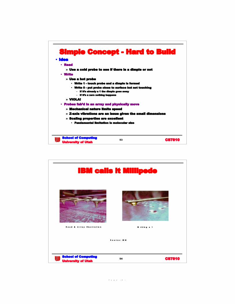
Probe Storage• Pioneered by IBM Zurich
Leverages AFM (atomic force microscope) technology Micro-machined cantilever to read and write indentations
in a polymer substrate
• Current demonstration density 641 Gb/in2
• Interestingly One of the current drivers of this technology is HP QSR?
P a g e ‹ # ›
53 CS7810School of ComputingUniversity of Utah
Simple Concept - Hard to Build• Idea
Read» Use a cold probe to see if there is a dimple or not
Write» Use a hot probe
• Write 1 - touch probe and a dimple is formed• Write 0 - put probe close to surface but not touching
– If it’s already a 1 the dimple goes away– If it’s a zero nothing happens
» VIOLA! Probes fab’d in an array and physically move
» Mechanical nature limits speed» Z-axis vibrations are an issue given the small dimensions» Scaling properties are excellent
• Fundamental limitation is molecular size
54 CS7810School of ComputingUniversity of Utah
IBM calls it Millipede
R e a d & A r r a y I l l u s t r a t i o n W r i t i n g a 1
S o u r c e : I B M
P a g e ‹ # ›
55 CS7810School of ComputingUniversity of Utah
Problems• Mechanical motion
Small makes it good BUT» Need to move the array likely slower than electrical
approach• Even at the scalable limit
• Yields Still experimental so device yield is off the chart low
• Role More likely a disk replacement than anything else
56 CS7810School of ComputingUniversity of Utah
Carbon Nanotube - NRAM• Least mature of the lot• Nantero owns most of the IP
Information more of a marketing blurb than anything else Have not found real publication data to date
» Hence no quantification or scaling properties» Numerous press releases which say the same thing
• Nantero claims Faster and denser than DRAM or FLASH Portable as FLASH Resistant to environment: temperature, magnetism

P a g e ‹ # ›
57 CS7810School of ComputingUniversity of Utah
Idea Basis• Sprinkle nanotubes over a silicon substrate• Pattern to create a bridge over a 13nm channel• Then
Read» Resistance based - usual sense amps etc.
Write» Bend the nanotube down to touch or not
• Van der Waals forces keep it bent
58 CS7810School of ComputingUniversity of Utah
StructureNonconductive spacers keepthe higher nanotubes flat andraised above the lower level.These spacers can bebetween five and tennanometers in height toseparate the layers ofnanotubes.These spacers must be tallenough to separate twolayers of nanotubes fromeach other when both are atrest, yet short enough toallow small charges toattract and cause bends inthe nanotubes.
S o u r c e : T h o m a s R u e c k e s , e t a l . , ” C a r b o n N a n o t u b e B a s e d N o n v o l a t i l e R a n d o m A c c e s s
M e m o r y
f o r M o l e c u l a r C o m p u t i n g ” , S C I E N C E , V O L 2 8 9 , 7 J U L Y 2 0 0 0 .

P a g e ‹ # ›
59 CS7810School of ComputingUniversity of Utah
Nantero NRAM
S o u r c e : N a n t e r o
60 CS7810School of ComputingUniversity of Utah
Structure
Fabricated on a silicon wafer, CNT ribbons are suspended 100nanometers above a carbon substrate layer.
S o u r c e : N a n t e r o
P a g e ‹ # ›
61 CS7810School of ComputingUniversity of Utah
NRAM Jury is Still Out• Concept is good - fab is problematic
5 nm gap between nano-tubes and channel hard to achieve Patterning must be very precise
» Tubes have to be thin enough and long enough to bendto create a contact
• Potential for universal memory Fast: 3 ns access demonstrated in 2006 by Nantero Scales: 22 nm demo in 2006
• But Commercial fab and a 1 cell lab test are miles apart
62 CS7810School of ComputingUniversity of Utah
RRAM - Resistive RAM• Missing Link (so far)
Lots of companies claim to be working on it» NTT, Sharp, Samsung, Fujitsu» Have yet to find performance and power numbers
• Obvious claims - low power, fast, high endurance
• Materials vary Perovskites (PCMO = Pr1-xCaxMnO3)
» Supply problem: Praseodymium is a rare earth metal Various transition metal oxides (groups 3-12) Chalcogenides (already covered in PCRAM part)
P a g e ‹ # ›
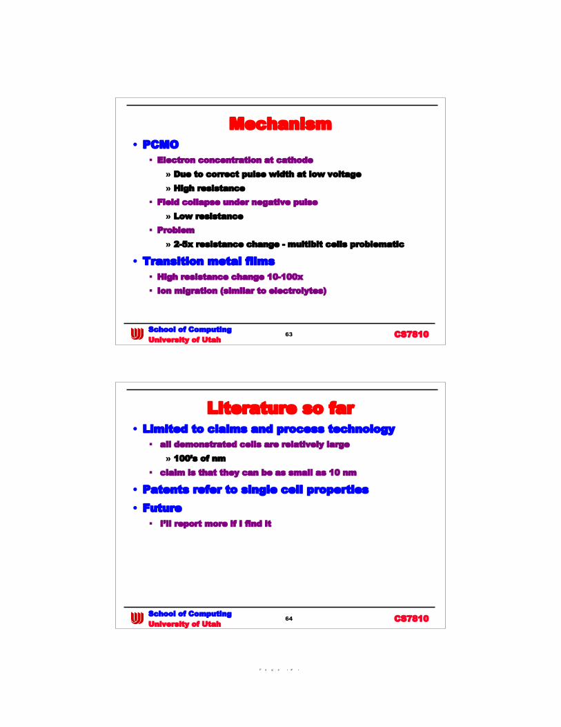
63 CS7810School of ComputingUniversity of Utah
Mechanism• PCMO
Electron concentration at cathode» Due to correct pulse width at low voltage» High resistance
Field collapse under negative pulse» Low resistance
Problem» 2-5x resistance change - multibit cells problematic
• Transition metal films High resistance change 10-100x Ion migration (similar to electrolytes)
64 CS7810School of ComputingUniversity of Utah
Literature so far• Limited to claims and process technology
all demonstrated cells are relatively large» 100’s of nm
claim is that they can be as small as 10 nm
• Patents refer to single cell properties• Future
I’ll report more if I find it
P a g e ‹ # ›
65 CS7810School of ComputingUniversity of Utah
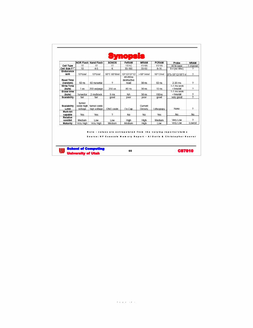
Synopsis
N o t e - v a l u e s a r e e x t r a p o l a t e d f r o m t h e v a r y i n g r e p o r t s / c l a i m s
S o u r c e : H P E x a s c a l e M e m o r y R e p o r t - A l D a v i s & C h r i s t o p h e r H o o v e r