Non-isolated Power Architecture With Diagnostics Reference ...
46
24 V 3.3 V 5 V Synchronous Buck Converter With Ultra-Low IQ 3.3 V 5 V LM5017 TPS54202 LM5165 TPS560430 TPS26624 LM2596S-adjevm LP87322Q1EVM 5 V 2 X DC-DC, 0.7 V to 3.36 V, 2 X LDO, 0.8 V to 3.3 V LMR36015 5 V TPS62821 TPS82740 TLV62084 1.5 V 3.3 V 3.3 V DC-DC with Hotrod package SN74LVC1G17 TVS3300 TVS3300 TVS3300 24 V 1.5 V Step-Down Converter with Eco-mode 2.5 V TPS82672 TLV62080 TPS73801D 1.2 V TPS54331 LMR33630 3.3 V TLV62569 LM2735X TPS560200 12 V 3.3 V TPS561201 3.3 V Synchronous Buck Converter With Ultra-Low EMI SN74LVC1G17 5 V 3.3 V 1 TIDUEP9 – June 2019 Submit Documentation Feedback Copyright © 2019, Texas Instruments Incorporated Non-isolated Power Architecture With Diagnostics Reference Design for Protection Relay Modules Design Guide: TIDA-010055 Non-isolated Power Architecture With Diagnostics Reference Design for Protection Relay Modules Description This reference design showcases non-isolated power supply architectures for protection relays with analog input/output and communication modules generated from 5-, 12-, or 24-V DC input. To generate the power supplies the design uses DC/DC converters with an integrated FET, a power module with an integrated inductor for size- and design-time-constrained applications, a HotRod™ package type for applications requiring low EMI and linear regulators (LDOs) for low ripple. Protections include a flat clamp TVS for input transient protection, an eFuse with configurable load current for overload protection and an ideal diode controller for input reversal protection. Additional features include an auto-switching power MUX, an analog temperature sensor, an input OK indication, a “no load” detection and a voltage supervisor. Resources TIDA-010055 Design Folder LM76002, LM5160, TPS7A39 Product Folder INA211-Q1, LMZ14202, TLV704 Product Folder TLV1117, TPS2662, REF3025 Product Folder TPS73801, TPS3840, LMZM23600 Product Folder TMP235, LM5017, LM5165, LMR36006 Product Folder TPS82740A, TLV62084, LM2735, SN74LVC1G17 Product Folder ASK Our E2E Experts WEBENCH® Calculator Tools Features • Power supplies for communication module: multiple non-isolated supply rails with varying load currents up to 1.5 A using a DC/DC converter with low I Q and EMI, DC/DC converter in HotRod™ package and DC/DC converter with Eco-mode™ • Power supplies for analog input/output modules: ±12-V split-rail supply for analog IO modules generated from a 24-V wide input synchronous buck converter, split rail DC/DC converters and LDOs and a ±10.5-V split-rail supply generated from 24 V using power modules with an integrated inductor in inverted buck configuration • Performance testing: Tested analog IO power supply performance by interfacing to high-accuracy AC analog input and DC analog output reference designs. Tested communication module power supply performance by interfacing to RS-485 EVMs (evaluation module), CAN EVMs, and 10/100 ethernet reference design, or 10/100/100 copper, or fiber interface EVM. • Pre-compliance testing: Tested power supply for electrical fast transients (EFT) and surge per IEC61000-4 and radiated emission per CISPR22 Applications • AC analog input module • Communication modules • Multifunction relay An IMPORTANT NOTICE at the end of this TI reference design addresses authorized use, intellectual property matters and other important disclaimers and information.
Transcript of Non-isolated Power Architecture With Diagnostics Reference ...

24 V
3.3 V
5 V
Synchronous Buck Converter With Ultra-Low IQ
3.3 V
5 V
LM5017
TPS54202
LM5165
TPS560430
TPS26624
LM2596S-adjevm LP87322Q1EVM
5 V
2 X DC-DC, 0.7 V to 3.36 V,2 X LDO, 0.8 V to 3.3 V
LMR36015 5 V TPS62821TPS82740TLV62084
1.5 V3.3 V3.3 V
DC-DC with Hotrod package
SN74LVC1G17
TVS3300TVS3300
TVS3300
24 V
1.5 VStep-Down Converter with Eco-mode
2.5 V
TPS82672
TLV62080
TPS73801D
1.2 VTPS54331
LMR33630 3.3 V
TLV62569
LM2735X
TPS560200
12 V
3.3 V
TPS561201 3.3 V
Synchronous Buck Converter With Ultra-Low EMI
SN74LVC1G17
5 V
3.3 V
1TIDUEP9–June 2019Submit Documentation Feedback
Copyright © 2019, Texas Instruments Incorporated
Non-isolated Power Architecture With Diagnostics Reference Design forProtection Relay Modules
Design Guide: TIDA-010055Non-isolated Power Architecture With DiagnosticsReference Design for Protection Relay Modules
DescriptionThis reference design showcases non-isolated powersupply architectures for protection relays with analoginput/output and communication modules generatedfrom 5-, 12-, or 24-V DC input. To generate the powersupplies the design uses DC/DC converters with anintegrated FET, a power module with an integratedinductor for size- and design-time-constrainedapplications, a HotRod™ package type for applicationsrequiring low EMI and linear regulators (LDOs) for lowripple. Protections include a flat clamp TVS for inputtransient protection, an eFuse with configurable loadcurrent for overload protection and an ideal diodecontroller for input reversal protection. Additionalfeatures include an auto-switching power MUX, ananalog temperature sensor, an input OK indication, a“no load” detection and a voltage supervisor.
Resources
TIDA-010055 Design FolderLM76002, LM5160, TPS7A39 Product FolderINA211-Q1, LMZ14202, TLV704 Product FolderTLV1117, TPS2662, REF3025 Product FolderTPS73801, TPS3840, LMZM23600 Product FolderTMP235, LM5017, LM5165, LMR36006 Product FolderTPS82740A, TLV62084, LM2735, SN74LVC1G17 Product Folder
ASK Our E2E ExpertsWEBENCH® Calculator Tools
Features• Power supplies for communication module: multiple
non-isolated supply rails with varying load currentsup to 1.5 A using a DC/DC converter with low IQand EMI, DC/DC converter in HotRod™ packageand DC/DC converter with Eco-mode™
• Power supplies for analog input/output modules:±12-V split-rail supply for analog IO modulesgenerated from a 24-V wide input synchronousbuck converter, split rail DC/DC converters andLDOs and a ±10.5-V split-rail supply generatedfrom 24 V using power modules with an integratedinductor in inverted buck configuration
• Performance testing: Tested analog IO powersupply performance by interfacing to high-accuracyAC analog input and DC analog output referencedesigns. Tested communication module powersupply performance by interfacing to RS-485 EVMs(evaluation module), CAN EVMs, and 10/100ethernet reference design, or 10/100/100 copper,or fiber interface EVM.
• Pre-compliance testing: Tested power supply forelectrical fast transients (EFT) and surge perIEC61000-4 and radiated emission per CISPR22
Applications• AC analog input module• Communication modules• Multifunction relay
An IMPORTANT NOTICE at the end of this TI reference design addresses authorized use, intellectual property matters and otherimportant disclaimers and information.

System Description www.ti.com
2 TIDUEP9–June 2019Submit Documentation Feedback
Copyright © 2019, Texas Instruments Incorporated
Non-isolated Power Architecture With Diagnostics Reference Design forProtection Relay Modules
1 System DescriptionFailure of power systems is one of the common problems faced by power generation, transmission, anddistribution companies. Power outages result in loss of revenue and reduce generation capacity. Powerutilities are working towards providing reliable power by using secondary equipment for protection, control,monitoring, and measurement systems to improve the power systems efficiency and reliability. The high-end secondary equipment used includes protection relay and terminal units such as remote terminal units,distribution terminal units, and feeder terminal units. Utility companies are also implementing andimproving multiple protection algorithms and diagnostic schemes to protect the assets and the grid, andpredict failures as early as possible. Signal processing and application processing including digital filtering,accurate measurement of analog inputs over wide input range, implementation of protection algorithms,user interface including LCD display, and implementing standard communication protocols based onIEC61850 standards.
For implementing applications including a user interface and standard communication protocols aprocessor with multiple cores and higher execution speed, standard Arm® architecture, external DDRmemory interface, and integrated peripherals simplifies the choice. The load current of the processor varywith execution speed, application, and transition between multiple operation modes resulting in widevariation in load current and the required power supply with fast transient load response. Since multiplerails are required, the power supply becomes complex increasing the solution size. Designing a powersupply solution with small form factor, higher efficiency to minimize internal heat and lower emission addsto other challenges during the design of communication module. Other challenges include protection of theDC inputs against output overload, diagnostics including voltage monitoring and load current monitoring.The power-supply architecture for the processor module is showcased in the High efficiency power supplyarchitecture reference design for protection relay processor module (TIDA-010011).
There are multiple modules in a protection relay. Analog modules are used for measurement of voltageand current inputs with input range of ±10.24 V or providing DC output voltage or current signal. Thesensor output is scaled using gain amplifiers to the ADC input range and require split power supplies.Additionally, for improved performance, low ripple outputs are required and are provided using dual LDOs.Communication modules provide multiple wired communication interface including Ethernet, RS232,RS485, and CAN. The communication modules also required a processor with MAC and multiple UARTs.The communication devices and processor requires multiple supply rails with varying load current. Therequired power supply rails for analog input, analog output, and communication modules are generated inthis reference design
The TIDA-010055 reference design address the previously-stated challenges and provides a solution thatcan be used during the design of a power supply for analog input/output and communication modulesresulting in reduced design efforts, faster time to market, high efficiency, and a small form factor.
This design can be used in multiple applications including:• Protection Relay: Protection relays detect defective lines, equipment, or other power system conditions
that are abnormal or dangerous in nature. Digital protection relays detect and locate faults bymeasuring electrical quantities in the power system, which is different during normal and intolerableconditions. To measure and protect different end equipment, protection relays interface to different IOsincluding AC analog inputs for measuring current and voltages, DC analog input or output for control,digital input or output for monitoring and interlocking , interface including Ethernet, RS232, RS485, andUSB for networking, HMI including LCD display or LEDs.
• Substation Automation and Merging unit: In substations, process-level primary equipment is monitoredusing RTU, bay controllers. The inputs to these equipment includes AC analog inputs for measuringcurrent and voltages, DC analog input or output for control, digital input or output for monitoring andinterlocking. Multiple communication options are also provided in this equipment for implementingautomation protocols. Since this equipment is installed in harsh environments, they are exposed toEMC and required to be protected against transients or other EMC for proper operation. Merging unitsare used to sample AC analog values on the process level in a substation and transmit the sampledvalues (SV) to protection devices, bay control units (BCU), or electric meters through fiber opticEthernet interface based on the IEC61850-9-2 protocol. A processor with the capability to sample theanalog inputs and process the samples is key to the design of the merging unit. Since this equipmentis installed near to the primary equipment, they are exposed to EMC and required to be protectedagainst transients or other EMC for proper operation.

www.ti.com System Description
3TIDUEP9–June 2019Submit Documentation Feedback
Copyright © 2019, Texas Instruments Incorporated
Non-isolated Power Architecture With Diagnostics Reference Design forProtection Relay Modules
1.1 Key System SpecificationsThe primary objective is to create a reference design platform to showcase different approaches togeneration of non-isolated power supply rails required for communication, analog input, and analog outputmodules from 24-V or 12-V or 5-V DC input using a DC/DC converter with integrated FET or powermodules with integrated inductor. The design additionally showcases operation of power supplies withwide input and high efficiency, generation of split-rail power supply using DC/DC converter and LDO,generation of stable reference with buffer, power MUXing two inputs, diagnostics, monitoring of loadcurrent and power supply rails.
Table 1. Power Supply for Analog IO Module SpecificationsPARAMETER DESCRIPTION SECTION
Supply generation using 24-V or 5-V input foranalog IO using DC/DC
24 V to 5 V, 5 V to load switch protected 5 V, input OK indication Section 2.3.1,Section 2.4.3Generation of supply rails including 5 V to ±14 V, ±14 V to ±12 V, 5 V to ±5 V
Generation of stable reference (series or shunt) with buffer
Onboard diagnostics using analog temperature sensor
Supply generation using 24-V input for analogIO using power module with input protection
Inverted buck configuration with 24 V to ±10.5 V using DC/DC power module Section 2.3.2,Section 2.4.2High efficiency 24 V to 5 V using DC/DC, 24-V eFuse with configurable load current, and
power supply status indication
Supply generation using 24-V input with inputreversal protection and no load detection
DC/DC input with reverse polarity protection, LDO and automatic power MUX , no loaddetection
Section 2.3.3
SIMPLE SWITCHER® and LDO for 5-V supply generation
Interface connector to EVM or other referencedesigns
Interface to TIDA-010034, TIDA-00946, TIDA-00928, TIDA-00227, TIDA-00226, TIDA-00834, TIDA-01633, ISO224EVM, PMP10618, PMP9379 to generate supply rails fromand evaluate performance of the generated power supplies
Table 2. Power Supply for Communication Module SpecificationsPARAMETER DESCRIPTION SECTION
Generation of multiple power supplies from 24-V input
Power supply generation (multiple supply rails with varying load current including 24 V, 5V and 3.3 V) using wide input DC/DC with input protection using eFuse
Section 2.3.4,Section 2.4.1,Section 2.4.2
Power supply generation (multiple supply rails with varying load current including 5 V,3.3 V, 1.8 V and 1.5 V) using synchronous step down converter with HotRod package
Power supply generation (multiple supply rails with varying load current including 24 V, 5V, and 3.3 V) using SIMPLE SWITCHER synchronous buck converter with ultra-low EMI
Power supply generation (multiple supply rails with varying load current including 3.3 V,2.5 V, 1.5 V and 1.2 V) using 3.5-V to 28-V input, 3-A, 570-kHz step-down converterwith Eco-mode
Interface to EVM LP87322Q1EVM, LM2596S-ADJEVM to generate supply rails from a and evaluateperformance of the generated power supplies
System Description www.ti.com
4 TIDUEP9–June 2019Submit Documentation Feedback
Copyright © 2019, Texas Instruments Incorporated
Non-isolated Power Architecture With Diagnostics Reference Design forProtection Relay Modules
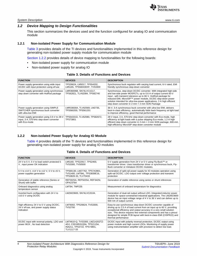
1.2 Device Mapping to Design FunctionalitiesThis section summarizes the devices used and the function configured for analog IO and communicationmodule
1.2.1 Non-isolated Power Supply for Communication ModuleTable 3 provides details of the TI devices and functionalities implemented in this reference design forgenerating non-isolated power supply module for communication module
Section 1.2.2 provides details of device mapping to functionalities for the following boards:• Non-isolated power supply for communication module• Non-isolated power supply for analog IO
Table 3. Details of Functions and DevicesFUNCTION DEVICES DESCRIPTION
Power supply generation using wide inputDC/DC with input protection using eFuse
TPS26624, LM5017, TPS54202,LM5165, TPS560430XF, TVS3300
Synchronous buck regulator with varying load current, 6-V rated, EMIfriendly synchronous step-down converter
Power supply generation using synchronousstep down converter with HotRod package
LMR36006B, SN74LVC1G17,TPS62821, TLV62084, TPS82740
Synchronous, step-down DC/DC converter. With integrated high-sideand low-side power MOSFETs, up to 0.6 A of output current 60-Vinput , with transient tolerance up to 66 V. HotRod package forreduced EMI, MicroSIP™ power module, DC/DC step-down powersolution intended for ultra-low-power applications, 2-A high efficientstep down converter in 2-mm × 2-mm SON Package
Power supply generation using SIMPLESWITCHER synchronous buck converterwith ultra-low EMI
LMR33630A, TLV62569, LM2735,TPS560200, TPS561201
36-V, 3-A synchronous buck converter with ultra-low EMI, deliversbest-in-class efficiency, automatically folds back frequency at light loadto improve efficiency, good thermal performance
Power supply generation using 3.5-V to 28-Vinput, 3 A, 570-kHz step-down converterwith Eco-mode
TPS54331D, TLV62080, TPS82672,TPS73801
28-V input, 3 A, 570-kHz step-down converter with Eco-mode, highefficiency at light loads with a pulse skipping Eco-mode, 1.2-A highefficient step down converter in 2-mm × 2-mm SON package, 600-mA,high-efficiency MicroSiP step-down converter module
1.2.2 Non-isolated Power Supply for Analog IO ModuleTable 4 provides details of the TI devices and functionalities implemented in this reference design forgenerating non-isolated power supply for analog IO modules
Table 4. Details of Functions and DevicesFUNCTION DEVICES DESCRIPTION
24 V to 5 V, 5 V to load switch protected 5V , input power OK indication
LM5160, TPS22917, TPS2400,TVS3300, TVS0500
5-V supply generation from 24 V or 5 V using Fly-Buck™ ortransformer driver. Uses transformer driver or synchronous buck, Fly-Buck converter or miniature DC/DC modules.
5 V to ±14 V, ±14 V to ±12 V, 5 V to ±5 V,power supplies generation
TPS65130, LM27762, TPS7A3901,TVS1400, LMT84L, TPS3839E16,TPS3828-33, TLV70433
Generation of split-rail power supply for IO modules operation usingsplit-rail DC/DC. LDO output over voltage protection and transientprotection
Generation of stable reference (Series orShunt) with buffer
REF3025A, REF5025A, REF3425I,OPA2376A
Generation of stable reference using series or shunt references
Onboard diagnostics using analogtemperature sensor
LMT84, TMP235 Measurement of onboard temperature for diagnostics
Inverted buck configuration with 24 V to±10.5 V using DC/DC
LMZM23600, SN74LVC2G34, Generation of dual-rail output without LDO. Integrated-inductor powermodule for space-constrained industrial applications. The LMZM23600device has an input voltage range of 4 V to 36 V and can deliver up to500 mA of output current.
High efficiency 24 V to 5 V using DC/DC,24-V eFuse, and power supply statusindication
LM76002, TPS26624, TVS3300,TVS2700
Easy-to-use synchronous step-down DC/DC converter capable ofdriving up to 2.5 A of load current from an input up to 60 V, providingexceptional efficiency and output accuracy in a very small solutionsize.. This device requires few external components and has a pinoutdesigned for simple PCB layout with best-in-class EMI (CISPR22) andthermal performance
DC/DC input with reversal polarity, LDO andpower MUX , No load detection
LM74610-Q, TVS3300, LMZ14202TZ-ADJ, CSD18531Q5A, TPS2115A,INA211, TPS3710, TPS73801,TLV1117-33
DC/DC input with polarity reversal protection, DC/DC output usingpower module and high current LDOs. Monitoring of supply powerusing instrumentation amplifier with provision to detect low load.
www.ti.com System Overview
5TIDUEP9–June 2019Submit Documentation Feedback
Copyright © 2019, Texas Instruments Incorporated
Non-isolated Power Architecture With Diagnostics Reference Design forProtection Relay Modules
Table 4. Details of Functions and Devices (continued)FUNCTION DEVICES DESCRIPTION
SIMPLE SWITCHER and LDO for 5-Vsupply generation
TPS560430, TPS7A0533 Simplest approach to power supply generation from 24 V,synchronous step-down DC/DC converter capable of driving up to600-mA load current, 36-V input
Interface to TO220 and TP247 modules orother reference designs
TPS54202 Interface to TIDA-00946, TIDA-00947, TIDA-00948, TIDA-00949,TIDA-010034 to generate multiple supply rails from a single 12-V or24-V DC input
2 System OverviewSome of the key requirements for design the power architecture for protection relay modules include:• Generation of the required supply rails (5 V to ±14 V, ±14 V to ±12 V, 5 V to ±5 V for analog IO and 5
V, 3,3 V, 2.5 V, 1.8 V and 1.2 V for communication) with high efficiency and scalable load current using5-, or 12-, or 24-V input using a DC/DC converter with integrated FET or power module with integratedinductor
• Isolating the output during input reversal and overload• Operation of the supply over wide range for applications using external auxiliary supply• Generation of stable reference (series or shunt) with buffer and low temperature drift• Onboard diagnostics using analog temperature sensor, input voltage status indication, load current
monitoring and voltage supervisor• Generation of split power supply (24 V to ±10.5 V) using DC/DC converter configured in inverted buck
configuration• Power supply for communication module using wide input DC/DC with input protection using eFuse• Power supply for communication module using synchronous step down converter with HotRod
package• Power supply for communication module using SIMPLE SWITCHER synchronous buck converter with
ultra-low EMI• Power supply for communication module using 3.5-V to 28-V input, 3-A, 570-kHz step-down converter
with Eco-mode• Protection of auxiliary supply input against voltage transients using flat clamp
The TIDA-010055 reference design provides solutions to the previously listed requirements and alsosolves some of the design challenges associated with the design of power architecture for protection relaymodules.
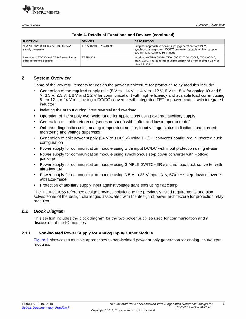
2.1 Block DiagramThis section includes the block diagram for the two power supplies used for communication and adiscussion of the IO modules.
2.1.1 Non-isolated Power Supply for Analog Input/Output ModuleFigure 1 showcases multiple approaches to non-isolated power supply generation for analog input/outputmodules.
TPS22917
TPS2400
TVS0500
TVS0500
LM5160
TVS0500
TVS3300
TPS65130
LM27761
TPS7A39
TLV70433
LMT84LPMTMP235 LM4040
REF3025REF3425REF5025
TPS3840DL30TPS3839TPS3828
OPA2376
TVS1400
TVS3300
TVS3300
TPS26624
TPS560430 TPS7A05
PMP9379
PMP10618
LM76002
LMZ14202TPS2115A
TPS73081
TLV1117
TVS3300
TVS0500LMZM23600
LMZM23600
LM74610CSD18531Q5A
SN74LVC2G34
INA211
LM4040
TPS3710
TVS1400
24 V
24 V
24 V
Synchronous Step-down DC/DC Converter 600 mA
eFuse
12 V or 24 V
24 VReversePolarityProtection
Dual-Supply Using Modules
10.5 V-10.5 VPG
LED buffer
No Load Detect
Power MUX 1-A LDOs
3.3 V
5 V
±12 V±15 V
3.3 V
5 V
Wide input 65 V, Synchronous buck/Fly-%XFN&RQYHUWHU
5 V
Input Voltage OK Voltage Supervisor
/RESET
RESET
Reference with Buffer
2.5 V
2.5 V
Dual-Supply LDOs
Synchronous Step-down DC/DC
SIMPLE SWITCHER® Power Module
±5 V±5 V±5 V
3.3 V
System Overview www.ti.com
6 TIDUEP9–June 2019Submit Documentation Feedback
Copyright © 2019, Texas Instruments Incorporated
Non-isolated Power Architecture With Diagnostics Reference Design forProtection Relay Modules
Figure 1. TIDA-010055 Non-isolated Power Supply for Analog IO Reference Design Block Diagram
2.1.1.1 Generation of Power-Supply Rails From 24-V InputThis design showcases the following functionalities:• Generation of 5-V DC power supply from 24-V input using wide input DC/DC converter• Generation of 5 V using power module with input reversal protection or synchronous step-down voltage
converter with eFuse protection• Generation of ±10.5-V from 24-V input using power module configured in inverted buck configuration
2.1.1.2 Generation of Power-Supply Rails From 5-V InputThis design showcases the following functionality:• Generation of split-rail ±15 V, ±12 V or ±5 V for operation of analog input or analog output modules• Protection of 5-V input against overload using load switch• Generation of required references with low drift from 5-V input
2.1.1.3 Generation of Clean Supply With Last-Stage LDOThis design showcases the following functionality:• Generation of 3.3 V from 5 V with varying load current (load current up to 1 A)• Automatic power MUX of 5-V inputs to the LDO from two different sources (power module or voltage
converter)
2.1.1.4 Input Protection Against TransientsThis design showcases protection of auxiliary DC input against transients using unidirectional orbidirectional flat clamp TVS.
24 V
3.3 V
5 V
Synchronous Buck Converter With Ultra-Low IQ
3.3 V
5 V
LM5017
TPS54202
LM5165
TPS560430
TPS26624
LM2596S-adjevm LP87322Q1EVM
5 V
2 X DC-DC, 0.7 V to 3.36 V,2 X LDO, 0.8 V to 3.3 V
LMR36015 5 V TPS62821TPS82740TLV62084
1.5 V3.3 V3.3 V
DC-DC with Hotrod package
SN74LVC1G17
TVS3300TVS3300
TVS3300
24 V
1.5 VStep-Down Converter with Eco-mode
2.5 V
TPS82672
TLV62080
TPS73801D
1.2 VTPS54331
LMR33630 3.3 V
TLV62569
LM2735X
TPS560200
12 V
3.3 V
TPS561201 3.3 V
Synchronous Buck Converter With Ultra-Low EMI
SN74LVC1G17
5 V
3.3 V
www.ti.com System Overview
7TIDUEP9–June 2019Submit Documentation Feedback
Copyright © 2019, Texas Instruments Incorporated
Non-isolated Power Architecture With Diagnostics Reference Design forProtection Relay Modules
2.1.1.5 Miscellaneous Diagnostic FunctionalitiesThis design showcases the following functionality• Voltage supervisor• Voltage detector• Analog temperature sensor• Input supply voltage OK indication• Buffering of the power good signal with LED drive for status indication onboard or remotely
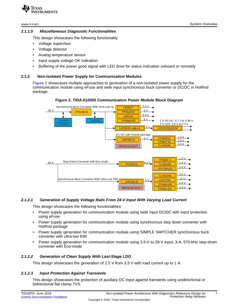
2.1.2 Non-isolated Power Supply for Communication ModulesFigure 2 showcases multiple approaches to generation of a non-isolated power supply for thecommunication module using eFuse and wide input synchronous buck converter or DC/DC in HotRodpackage.
Figure 2. TIDA-010055 Communication Power Module Block Diagram
2.1.2.1 Generation of Supply Voltage Rails From 24-V Input With Varying Load CurrentThis design showcases the following functionalities:• Power supply generation for communication module using wide input DC/DC with input protection
using eFuse• Power supply generation for communication module using synchronous step down converter with
HotRod package• Power supply generation for communication module using SIMPLE SWITCHER synchronous buck
converter with ultra-low EMI• Power supply generation for communication module using 3.5-V to 28-V input, 3-A, 570-kHz step-down
converter with Eco-mode
2.1.2.2 Generation of Clean Supply With Last-Stage LDOThis design showcases the generation of 2.5 V from 3.3 V with load current up to 1 A.
2.1.2.3 Input Protection Against TransientsThis design showcases the protection of auxiliary DC input against transients using unidirectional orbidirectional flat clamp TVS.
System Overview www.ti.com
8 TIDUEP9–June 2019Submit Documentation Feedback
Copyright © 2019, Texas Instruments Incorporated
Non-isolated Power Architecture With Diagnostics Reference Design forProtection Relay Modules
2.1.2.4 Miscellaneous Power FunctionalitiesThis section showcases the buffering of the power good signal with LED drive for status indicationonboard or remotely.
2.1.3 Details of TI Devices Used With Links to TI.comTable 5 lists the TI devices used and the links to TI.com
Table 5. TI Devices Used and TI.com Links
TI.com LINKS DEVICESLM5160, LM27762, TPS7A39, TPS65130 DC/DC and LDOREF3025, OPA2376, REF5025, LM4040 Op amp and referenceLMT84, TMP235, TVS3300, TVS0500 Temperature sensor, and flat clamp TVSTPS2662, TPS2115A, LMZ14202, TLV1117 eFuse, power MUX, DC/DC converter
LM74610-Q1, TPS2400 , LM76002, INA211 Ideal diode controller, comparator, DC/DC and instrumentationamplifier
TPS73801, TPS3710, TPS3839, TPS3828 LDO and voltage supervisorLMZM23600, TVS1400, TVS2700, SN74LVC2G34 DC/DC, flat clamp TVS and buffer for LED indicationTPS22917, TPS560430, TPS7A05, CSD18504Q5A Load switch, DC/DC, LDO and MOSFETTLV704, REF3425, TPS3840, LM5017 LDO, reference and DC/DCTPS54202, LM5165, LMR36006, TPS62821 DC/DCTLV62080, TPS54331, TLV62569, LMR33630 DC/DCSN74LVC1G17, SN74LVC1G07, TPS560200, TPS561201 Logic and DC/DCTPS826721, TPS82740A, TLV62084, CSD17571Q2 DC/DC and MOSFETLM2735 DC/DC
2.1.4 Interface to EVMThe design additionally provides a provision to connect to external devices and test the performance usingevaluation modules.
2.2 Design ConsiderationsSome of the key considerations for this design include:• Using wide input DC/DC converters with integrated FET or power modules with integrated inductor for
generation of the required DC power supply rails providing cost and size optimized option• Using buck converters with integrated inductor with high efficiency, improving reliability in size-
constrained application• Using buck converters with integrated switch in HotRod package for reduced EMI in applications
requiring high performance• Point-of-load power supply with high efficiency for generating low voltage and high current rails• Generation of split-rail power supplies for analog IO modules using split-rail DC/DC and dual LDO• Generation of split-rail power supply using power modules fo high efficiency and output load current
with the power module configured as inverter buck• Power supply diagnostics including power supply monitoring, and power supply switching using load
switches• Onboard temperature sensors for protection and diagnostics
This is a generic design focusing on the generation of power supply rails for protection relay modules andcan be used across other end equipment in grid infrastructure and other adjacent sectors including motordrives, factory and building automation, test and measurement, and medical sectors.
www.ti.com System Overview
9TIDUEP9–June 2019Submit Documentation Feedback
Copyright © 2019, Texas Instruments Incorporated
Non-isolated Power Architecture With Diagnostics Reference Design forProtection Relay Modules
2.2.1 DC/DC Converter With Internal FET or Power Module With Integrated Inductor AdvantagesDC/DC buck modules integrate inductors, FETs, compensation, and other passive components into asingle package to simplify the design process and speed customer time-to-market with a minimizedpower-supply footprint. Power modules are gaining popularity with the ensured EMI and EMC as well asfull characterized electrical and thermal performance and ease of prototyping. Step-down buck powermodules offer superior performance against alternative solutions while also helping fasten the design andqualification process to help get to market faster.
Advantages of the power module include:• Simpler solution, small size, and high power density with minimum external components• High efficiency and output accuracy, good load-transient response and low output ripple• Single family of devices can support multiple power supply rails due to programmability• Improved load and input regulation• Quick, easy to design, use, and minimizes external components• Reliable, low radiated EMI and cooler operating temperature
2.3 Highlighted ProductsThis section provides details of some of the TI products used in this reference design for generation ofrequired power supplies for protection relay modules.
2.3.1 Supply Generation Using 24-V Input or 5 V for Analog IO Module Using DC/DCThis section provides details of the devices used to generate analog input/output supplies, reference andmonitoring of the supplies using wide input DC/DC converter with integrated FET.
2.3.1.1 24 V to 5 V, 5 V to Load-Switch Protected 5-V, Input Power OKThe 24 V to 5 V, 5 V to load-switch protected 5-V, input power OK functionality is implemented using thefollowing devices:• LM5160, wide input 65-V, 2-A synchronous buck, Fly-Buck converter• TPS22917, ultra-low leakage, 5.5-V, 2-A, 80-mΩ on-resistance load switch• TPS2400, 5.5-V overvoltage protection controller with 100-V input transient protection• TVS3300, 33-V flat-clamp surge protection device• TVS0500, 5-V flat-clamp surge protection device
2.3.1.2 5 V to ±14 V, ±14 V to ±12 V, 5 V to ±5 V, Power Supplies GenerationThe 5 V to ±14 V, ±14 V to ±12 V, 5 V to ±5 V, power supplies generation functionality is implementedusing the following devices:• TPS65130, split-rail converter with dual, positive and negative outputs (300 mA typ)• LM27762, low-noise positive- and negative-output charge pump with integrated LDO• TPS7A3901, dual, 150-mA, wide-VIN, positive and negative low-dropout (LDO) voltage regulator• TPS3839E16, ultra-low power, supply voltage supervisor• TPS3828-33, voltage monitor with watchdog timer• TLV70433, 24-V input voltage, 150-mA, ultra-low-IQ low-dropout (LDO) regulator• TVS1400, 14-V flat-clamp surge protection device
System Overview www.ti.com
10 TIDUEP9–June 2019Submit Documentation Feedback
Copyright © 2019, Texas Instruments Incorporated
Non-isolated Power Architecture With Diagnostics Reference Design forProtection Relay Modules
2.3.1.3 Generation of Stable Reference (Series or Shunt) With BufferThe generation of stable reference (series or shunt) with buffer functionality is implemented using thefollowing devices:• REF3025A, 2.5-V 50-ppm/°C, 50 µA in SOT23-3 series (bandgap) voltage reference• REF5025A, 3 µVpp/V noise, 3-ppm/°C drift precision series voltage reference• REF3425I, 2.5-V low-drift low-power small-footprint series voltage reference• OPA2376A, precision, low-noise, low quiescent current operational amplifier
2.3.1.4 Onboard Diagnostics Using Analog Temperature SensorThe onboard diagnostics using analog temperature sensor functionality is implemented using the followingdevices:• TMP235, precision analog output temperature sensor• LMT84L, 1.5 V-capable, 10-µA analog output temperature sensor
2.3.2 Supply Generation Using 24-V Input for Analog IO Using Power Module With Input ProtectionThis section provides details of the devices used to generate analog input/output supplies using a powermodule in inverter buck configuration, automatic power MUX, input reversal protection and overloadprotection.
2.3.2.1 Inverted Buck Configuration With 24 V to ±10.5 V Using DC/DCThe inverted buck configuration with 24 V to ±10.5 V using DC/DC functionality is implemented using thefollowing devices:• LMZM23600, 36-V, 0.5-A step-down DC/DC power module• SN74LVC2G34, dual buffer gate• CSD17585F5T, 30 V N-channel FemtoFET™ MOSFET
2.3.2.2 High-Efficiency, 24 V to 5 V Using DC/DC, 24-V eFuse, and Power-Supply Status IndicationThe high-efficiency 24 V to 5 V using DC/DC, 24-V eFuse, and power-supply status indication functionalityis implemented using the following devices:• LM76002, 3.5-V to 60-V, 2.5-A synchronous step-down voltage converter• TPS26624, 60-V 800-mA industrial eFuse with integrated reverse polarity protection• TVS3300, 33-V flat-clamp surge protection device• TVS2700, 27-V flat-clamp surge protection device

www.ti.com System Overview
11TIDUEP9–June 2019Submit Documentation Feedback
Copyright © 2019, Texas Instruments Incorporated
Non-isolated Power Architecture With Diagnostics Reference Design forProtection Relay Modules
2.3.3 Supply Generation Using 24-V Input With Input Reversal Protection and No-Load DetectionThis section showcases generation of the required supply rails from 24-V input with input reversalprotection.
2.3.3.1 DC/DC Input With Reversal Polarity, LDO and Power MUX and No-Load DetectionThe DC/DC input with reversal polarity, LDO and power MUX and no-load detection functionality isimplemented using the following devices:• LM74610-Q, Zero IQ reverse polarity protection smart diode controller• LMZ14202TZ-ADJ, SIMPLE SWITCHER 6-V to 42-V, 2-A power module in leaded SMT-TO package• CSD18531Q5A, 60 V N-channel NexFET™ power MOSFETs, CSD18531Q5A• TPS2115A, auto-switching power MUX• INA211, 26-V, bidirectional, zero-drift, low-side, high-side, voltage output current sense amplifier• TPS3710, wide-VIN voltage detector• TPS73801, 1-A, low-noise, fast transient response low-dropout linear regulator• TLV1117-33, single output LDO, 800-mA, fixed and adjustable, internal current limit, thermal overload
protection• TVS3300, 33-V flat-clamp surge protection device
2.3.3.2 SIMPLE SWITCHER® and LDO for 5-V Supply GenerationThe SIMPLE SWITCHER and LDO for 5-V supply generation functionality is implemented using thefollowing devices:• TPS560430, SIMPLE SWITCHER 36-V, 600-mA buck regulator with high-efficiency sleep mode, 1.1
MHz, FPWM, adjustable• TPS7A0533, 1-µA, ultra-low IQ, 200-mA low-dropout (LDO) regulator in a small-size package
2.3.4 Generation of Power Supplies for Communication Module From 24-V InputThis section provides details of the devices used to generate different power rails for communicationmodule from 24-V input with overload protection.
2.3.4.1 Power-Supply Generation Using Wide Input DC/DC With Input Protection Using eFuseThe following devices have been used to generate the required supply rails:• TPS26624, 60-V 800-mA industrial eFuse with integrated reverse polarity protection• LM5017, 7.5 V to 100 V wide VIN, 600-mA constant on-time synchronous buck regulator• LM5165, 3-V to 65-V, 150-mA synchronous buck converter with ultra-low IQ
• TPS560430, SIMPLE SWITCHER 36-V, 600-mA buck regulator with high-efficiency sleep mode, 1.1MHz, FPWM, adjustable
• TVS3300, 33-V flat-clamp surge protection device
2.3.4.2 Power-Supply Generation Using Synchronous Step-Down Converter With HotRod™ PackageThe following devices have been used to generate the required supply rails:• LMR36006, 4.2-V to 60-V, 0.6-A ultra-small synchronous step-down converter• TPS62821, 1-A step-down converter with 1% accuracy in 1.5-mm × 2-mm QFN• TLV62084, 2-A high efficient step down converter in 2-mm × 2-mm SON package• TPS82740, 200-mA step-down converter module with 360-nA IQ
• SN74LVC1G17, single Schmitt-trigger buffer
System Overview www.ti.com
12 TIDUEP9–June 2019Submit Documentation Feedback
Copyright © 2019, Texas Instruments Incorporated
Non-isolated Power Architecture With Diagnostics Reference Design forProtection Relay Modules
2.3.4.3 Power-Supply Generation Using SIMPLE SWITCHER® Synchronous Buck Converter With Ultra-Low EMI
The following devices have been used to generate the required supply rails:• LMR33630, SIMPLE SWITCHER 3.8 V to 36 V, 3-A synchronous buck converter with ultra-low EMI• TLV62569, 2-A high-efficiency step-down buck converter in SOT23 and SOT563 package• LM2735, 520-kHz/1.6-MHz - space-efficient boost and SEPIC DC/DC regulator• TPS560200, 17-V input, 500-mA synchronous step-down regulator in SOT-23 with advanced Eco-
Mode• TPS561201, 4.5-V to 17-V input, 1-A synchronous step-down voltage regulator in 6-pin SOT-23
2.3.4.4 Power-Supply Generation Using 3.5-V to 28-V Input, 3-A, 570-kHz Step-Down Converter WithEco-mode™
The following devices have been used to generate the required supply rails:• TPS5433, 13.5-V to 28-V input, 3-A, 570-kHz step-down converter with Eco-mode• TLV62080, 1.2-A high efficient step down converter in 2-mm × 2-mm SON package• TPS82672, 600-mA, high-efficiency MicroSiP step-down converter module (profile < 1.0 mm)• TPS73801, 1-A low noise, fast transient response low-dropout linear regulator
2.3.5 EnhancementsThis section provides information on some of the design enhancements that can be considered during thedesign of the processor power modules and also provides a few commonly used devices.
2.3.5.1 Leveraging Other Reference DesignsThe following list of reference designs can be leveraged during the design of power supply rails for theprocessor module.• IIEEE802.3at Type-1 PoE and 12-V adapter input to point of load reference design for IP network
camera• 32-bit Arm® Cortex®-M4F MCU based Small form factor Serial-to-Ethernet Converter• Small Form Factor 12W Ultra Wide Range Power Supply for Protection Relays - Reference Design• High Accuracy Analog Front End Using 16-Bit SAR ADC with ±10V Measurement Range Reference
Design• Compact Programmable 4-20mA and ±10V Analog Output Reference Design for AC/Servo Drives• 5-V 1A, Low EMI, 94% Efficiency DC/DC Module in Dual Layer TO-220 Form Factor Reference Design• EMI/EMC Compliant 10/100 Mbps Ethernet Brick with Fiber or Twisted Pair Interface Reference
Design• ISO224 evaluation module• LP873220-Q1 Dual High-Current Buck Converters and Dual Linear Regulator Evaluation Module• LM2596 Step-Down Converter Evaluation Module• 15- to 60V Wide Input Four-Output SIMPLE SWITCHER® Reference Design Using LM46002 and
LMZ21701• Positive/Negative 15-V Output Supply Using Wide Vin Synchronous Buck Regulator Reference Design• Low noise power-supply reference design maximizing performance in 12.8 GSPS data acquisition
systems• Multi-rail TV power supply reference design, with flexible partitioning to maximize power savings• VBus protection with eFuse for solid state drive modules reference design
www.ti.com System Overview
13TIDUEP9–June 2019Submit Documentation Feedback
Copyright © 2019, Texas Instruments Incorporated
Non-isolated Power Architecture With Diagnostics Reference Design forProtection Relay Modules
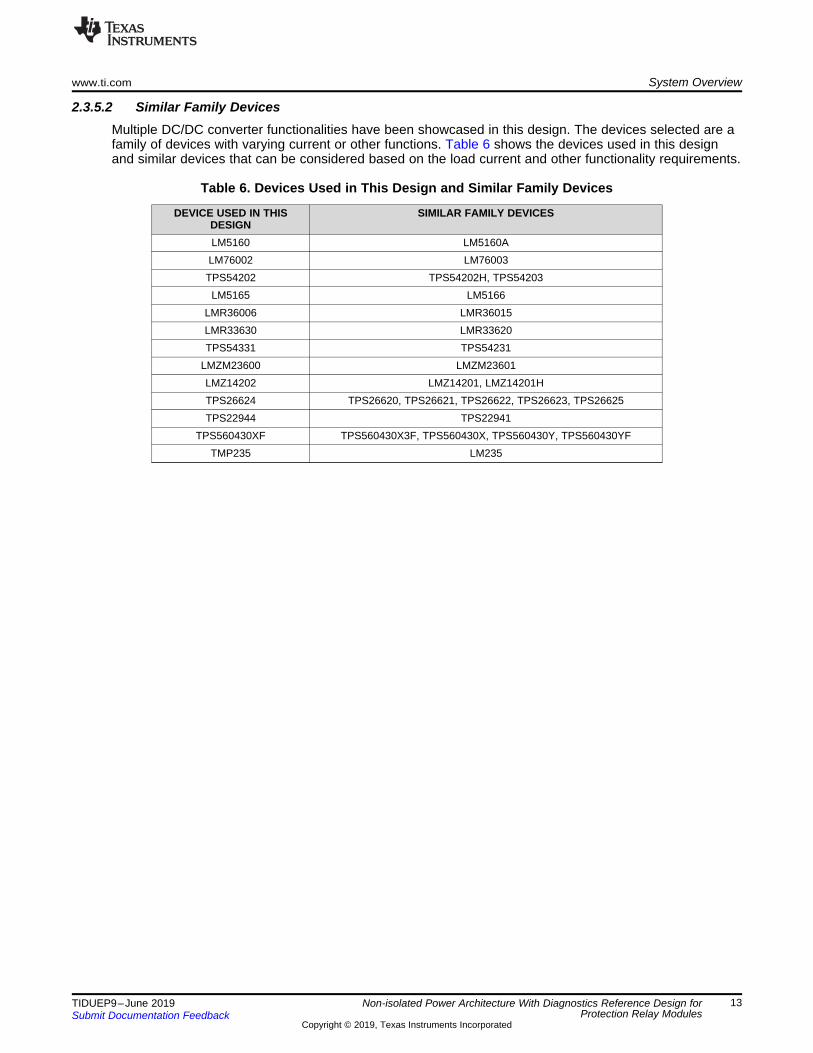
2.3.5.2 Similar Family DevicesMultiple DC/DC converter functionalities have been showcased in this design. The devices selected are afamily of devices with varying current or other functions. Table 6 shows the devices used in this designand similar devices that can be considered based on the load current and other functionality requirements.
Table 6. Devices Used in This Design and Similar Family Devices
DEVICE USED IN THISDESIGN
SIMILAR FAMILY DEVICES
LM5160 LM5160ALM76002 LM76003TPS54202 TPS54202H, TPS54203LM5165 LM5166
LMR36006 LMR36015LMR33630 LMR33620TPS54331 TPS54231
LMZM23600 LMZM23601LMZ14202 LMZ14201, LMZ14201HTPS26624 TPS26620, TPS26621, TPS26622, TPS26623, TPS26625TPS22944 TPS22941
TPS560430XF TPS560430X3F, TPS560430X, TPS560430Y, TPS560430YFTMP235 LM235
System Overview www.ti.com
14 TIDUEP9–June 2019Submit Documentation Feedback
Copyright © 2019, Texas Instruments Incorporated
Non-isolated Power Architecture With Diagnostics Reference Design forProtection Relay Modules
2.4 System Design TheoryThe design is split into the following two boards:• Power supply architecture for communication modules• Power supply architecture for analog input/output modules
The following sections provide details of the circuit design and implementation:
2.4.1 Power Supplies for Communication Modules With Input Connected to J2This section describes approaches for generation of power supply rails from 24-V DC input forcommunication modules with input connected to J2.
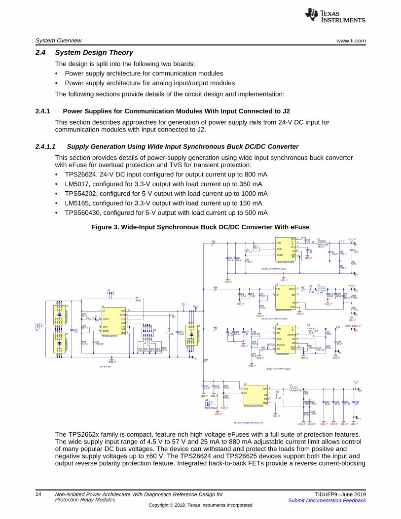
2.4.1.1 Supply Generation Using Wide Input Synchronous Buck DC/DC ConverterThis section provides details of power-supply generation using wide input synchronous buck converterwith eFuse for overload protection and TVS for transient protection:• TPS26624, 24-V DC input configured for output current up to 800 mA• LM5017, configured for 3.3-V output with load current up to 350 mA• TPS54202, configured for 5-V output with load current up to 1000 mA• LM5165, configured for 3.3-V output with load current up to 150 mA• TPS560430, configured for 5-V output with load current up to 500 mA
Figure 3. Wide-Input Synchronous Buck DC/DC Converter With eFuse
The TPS2662x family is compact, feature rich high voltage eFuses with a full suite of protection features.The wide supply input range of 4.5 V to 57 V and 25 mA to 880 mA adjustable current limit allows controlof many popular DC bus voltages. The device can withstand and protect the loads from positive andnegative supply voltages up to ±60 V. The TPS26624 and TPS26625 devices support both the input andoutput reverse polarity protection feature. Integrated back-to-back FETs provide a reverse current-blocking
www.ti.com System Overview
15TIDUEP9–June 2019Submit Documentation Feedback
Copyright © 2019, Texas Instruments Incorporated
Non-isolated Power Architecture With Diagnostics Reference Design forProtection Relay Modules
feature making the device suitable for systems with output voltage holdup requirements during power failand brownout conditions. Load, source, and device protection are provided with many adjustable featuresincluding overcurrent, output slew rate, and overvoltage and undervoltage thresholds. The internal robustprotection control blocks along with the high-voltage rating of the TPS2662x family helps to simplify thesystem designs for surge protection
The TPS560430 is an easy-to-use synchronous step-down DC/DC converter capable of driving up to a600-mA load current. With a wide input range of 4 V to 36 V, the device is suitable for a wide range ofapplications. The TPS560430 has 1.1-MHz and 2.1-MHz operating frequency versions for either highefficiency or small solution size. The TPS560430 also has an FPWM (forced PWM) version to achieveconstant frequency and small output voltage ripple over the full load range. Soft-start and compensationcircuits are implemented internally which allows the device to be used with minimum external components.The device has built-in protection features, such as cycle-by-cycle current limit, hiccup mode short-circuitprotection, and thermal shutdown in case of excessive power dissipation.

System Overview www.ti.com
16 TIDUEP9–June 2019Submit Documentation Feedback
Copyright © 2019, Texas Instruments Incorporated
Non-isolated Power Architecture With Diagnostics Reference Design forProtection Relay Modules
2.4.1.2 Power-Supply Generation Using DC/DC Converter in HotRod™ PackageThis section provides implementation details of power supply generation using DC/DC converter inHotRod™ package providing lower emission:• LMR36006, configured for 5-V output with load current up to 500 mA• TPS62821, configured for 1.5-V output with load current up to 925 mA• TLV62084, configured for 1.8-V output with load current up to 1000 mA• TPS82740, configured for 3.3-V output with load current up to 1000 mA• SN74LVC1G07, used for buffering power good output for diagnostics
Figure 4. DC/DC Converter With HotRod™ Package
The LMR36006 regulator is an easy-to-use, synchronous, step-down DC/DC converter. With integratedhigh-side and low-side power MOSFETs, up to 0.6 A of output current is delivered over a wide inputvoltage range of 4.2 V to 60 V. Tolerance goes up to 66 V. The transient tolerance reduces the necessarydesign effort to protect against overvoltages and meets the surge immunity requirements of IEC 61000-4-5. The LMR36006 uses peak-current-mode control to provide optimal efficiency and output voltageaccuracy. Precision enable gives flexibility by enabling a direct connection to the wide input voltage orprecise control over device start-up and shutdown. The power-good flag, with built-in filtering and delay,offers a true indication of system status eliminating the requirement for an external supervisor.
The LMR36006 is in a HotRod package which enables low noise, higher efficiency, and the smallestpackage to die ratio. The device requires few external components and has a pinout designed for simplePCB layout.
www.ti.com System Overview
17TIDUEP9–June 2019Submit Documentation Feedback
Copyright © 2019, Texas Instruments Incorporated
Non-isolated Power Architecture With Diagnostics Reference Design forProtection Relay Modules
2.4.2 Power Supplies for Communication Modules With Input Connected to J5This section describes approaches for generation of power supply rails from 24-V DC input forcommunication modules with input connected to J5.
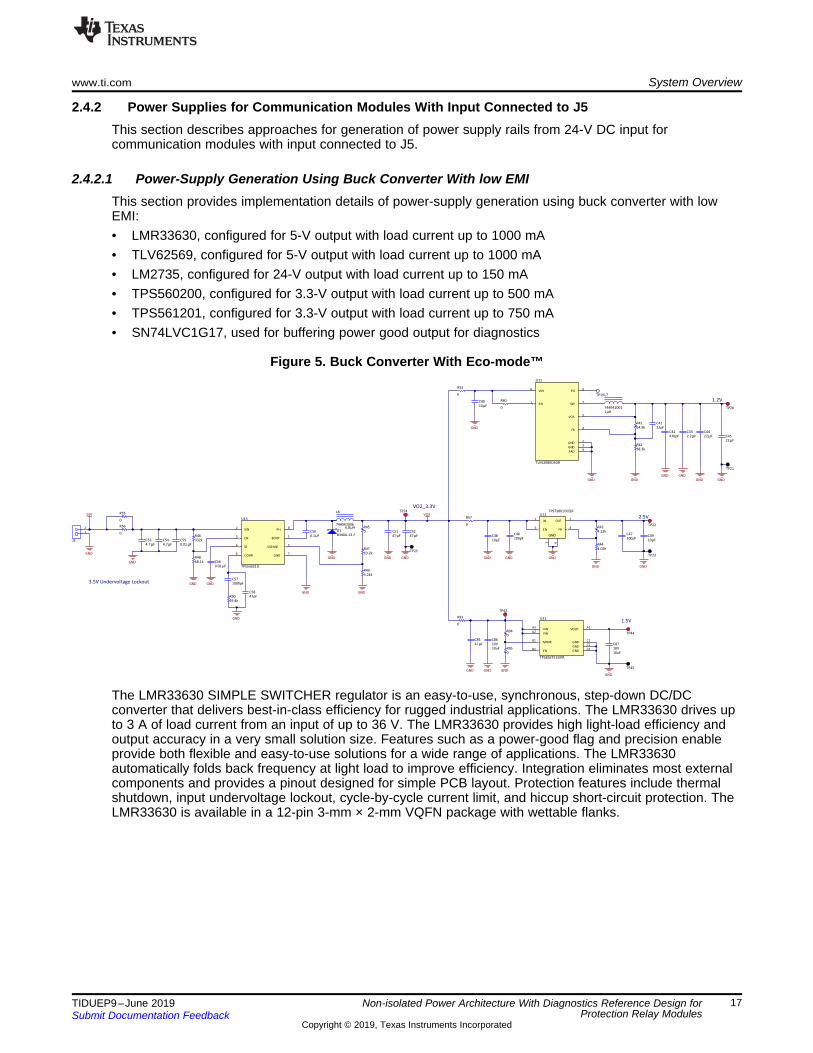
2.4.2.1 Power-Supply Generation Using Buck Converter With low EMIThis section provides implementation details of power-supply generation using buck converter with lowEMI:• LMR33630, configured for 5-V output with load current up to 1000 mA• TLV62569, configured for 5-V output with load current up to 1000 mA• LM2735, configured for 24-V output with load current up to 150 mA• TPS560200, configured for 3.3-V output with load current up to 500 mA• TPS561201, configured for 3.3-V output with load current up to 750 mA• SN74LVC1G17, used for buffering power good output for diagnostics
Figure 5. Buck Converter With Eco-mode™
The LMR33630 SIMPLE SWITCHER regulator is an easy-to-use, synchronous, step-down DC/DCconverter that delivers best-in-class efficiency for rugged industrial applications. The LMR33630 drives upto 3 A of load current from an input of up to 36 V. The LMR33630 provides high light-load efficiency andoutput accuracy in a very small solution size. Features such as a power-good flag and precision enableprovide both flexible and easy-to-use solutions for a wide range of applications. The LMR33630automatically folds back frequency at light load to improve efficiency. Integration eliminates most externalcomponents and provides a pinout designed for simple PCB layout. Protection features include thermalshutdown, input undervoltage lockout, cycle-by-cycle current limit, and hiccup short-circuit protection. TheLMR33630 is available in a 12-pin 3-mm × 2-mm VQFN package with wettable flanks.

System Overview www.ti.com
18 TIDUEP9–June 2019Submit Documentation Feedback
Copyright © 2019, Texas Instruments Incorporated
Non-isolated Power Architecture With Diagnostics Reference Design forProtection Relay Modules
2.4.2.2 Small-Size Buck Converter With Eco-mode™This section provides implementation details of power supply generation using small size buck converterwith Eco-mode:• TPS54331, configured for 5-V output with load current up to 1000 mA• TLV62080, configured for 1.2-V output with load current up to 950 mA• TPS82672, configured for 1.5-V output with load current up to 300 mA• TPS73801, configured for 2.5-V output with load current up to 750 mA
Figure 6. Buck DC/DC Converter low EMI
The TLV6208x family devices are small buck converters with few external components, enabling cost-effective solutions. They are synchronous step-down converters with an input voltage range of 2.5 and 2.7(2.5 V for TLV62080, 2.7 V for TLV62084x) to 6 V. The TLV6208x devices focus on high-efficiency step-down conversion over a wide output current range. At medium to heavy loads, the TLV6208x convertersoperate in PWM mode and automatically enter power save mode operation at light-load currents tomaintain high efficiency over the entire load current range. To address the requirements of system powerrails, the internal compensation circuit allows a wide range of external output capacitor values. With theDCS-Control™ (Direct Control with Seamless transition into Power save mode) architecture excellent loadtransient performance and output voltage regulation accuracy are achieved.
www.ti.com System Overview
19TIDUEP9–June 2019Submit Documentation Feedback
Copyright © 2019, Texas Instruments Incorporated
Non-isolated Power Architecture With Diagnostics Reference Design forProtection Relay Modules
2.4.3 Power-Supply Generation for Analog Input/Output Modules Using DC/DCThis section describes generation of 5 V using DC/DC converter and protection of 5-V output using loadswitch with the inputs connected to J4 and J1.
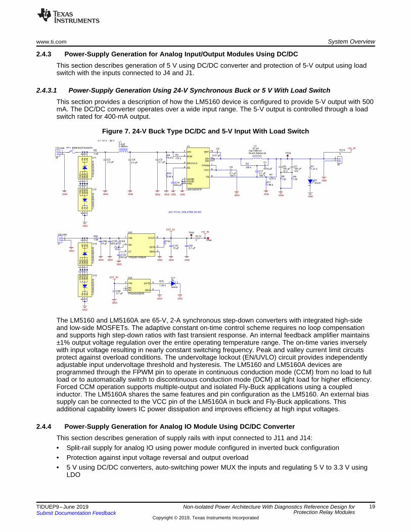
2.4.3.1 Power-Supply Generation Using 24-V Synchronous Buck or 5 V With Load SwitchThis section provides a description of how the LM5160 device is configured to provide 5-V output with 500mA. The DC/DC converter operates over a wide input range. The 5-V output is controlled through a loadswitch rated for 400-mA output.
Figure 7. 24-V Buck Type DC/DC and 5-V Input With Load Switch
The LM5160 and LM5160A are 65-V, 2-A synchronous step-down converters with integrated high-sideand low-side MOSFETs. The adaptive constant on-time control scheme requires no loop compensationand supports high step-down ratios with fast transient response. An internal feedback amplifier maintains±1% output voltage regulation over the entire operating temperature range. The on-time varies inverselywith input voltage resulting in nearly constant switching frequency. Peak and valley current limit circuitsprotect against overload conditions. The undervoltage lockout (EN/UVLO) circuit provides independentlyadjustable input undervoltage threshold and hysteresis. The LM5160 and LM5160A devices areprogrammed through the FPWM pin to operate in continuous conduction mode (CCM) from no load to fullload or to automatically switch to discontinuous conduction mode (DCM) at light load for higher efficiency.Forced CCM operation supports multiple-output and isolated Fly-Buck applications using a coupledinductor. The LM5160A shares the same features and pin configuration as the LM5160. An external biassupply can be connected to the VCC pin of the LM5160A in buck and Fly-Buck applications. Thisadditional capability lowers IC power dissipation and improves efficiency at high input voltages.
2.4.4 Power-Supply Generation for Analog IO Module Using DC/DC ConverterThis section describes generation of supply rails with input connected to J11 and J14:• Split-rail supply for analog IO using power module configured in inverted buck configuration• Protection against input voltage reversal and output overload• 5 V using DC/DC converters, auto-switching power MUX the inputs and regulating 5 V to 3.3 V using
LDO

System Overview www.ti.com
20 TIDUEP9–June 2019Submit Documentation Feedback
Copyright © 2019, Texas Instruments Incorporated
Non-isolated Power Architecture With Diagnostics Reference Design forProtection Relay Modules
2.4.4.1 Power Module Configured in Inverted Buck Configuration With eFuse ProtectionThe required supply rails are generated using the following DC/DC:• LMZM23600, configured for ±10.5 V with 350--mA load current• LM76002, configured for 5 V with 1250-mA load current• TPS26624, 24-V DC input with up to 800-mA output load current
Figure 8. Inverted Buck Power Module With eFuse Protection
The LM7600X regulator is an easy-to-use synchronous step-down DC/DC converter capable of driving upto 2.5 A (LM76002) or 3.5 A (LM76003) of load current from an input up to 60 V. The LM76002 providesexceptional efficiency and output accuracy in a very small solution size. Peak current-mode control isemployed. Additional features such as adjustable switching frequency, synchronization, FPWM option,power-good flag, precision enable, adjustable soft start, and tracking provide both flexible and easy-to-usesolutions for a wide range of applications. Automatic frequency foldback at light load and optional externalbias improve efficiency. This device requires few external components and has a pinout designed forsimple PCB layout with best-in-class EMI (CISPR22) and thermal performance. Protection features includeinput undervoltage lockout, thermal shutdown, cycle-by-cycle current limit, and short-circuit protection.
The LMZM23600 integrated-inductor power module is specifically designed for space-constrainedindustrial applications. It is available in two fixed output voltage options of 5-V and 3.3-V, and anadjustable (ADJ) output voltage option supporting a 2.5-V to 15-V range. The LMZM23600 has an inputvoltage range of 4-V to 36-V and can deliver up to 500-mA of output current. This power module isextremely easy to use, requiring only 2 external components for a 5-V or 3.3-V output design. All aspectsof the LMZM23600 are optimized for performance driven and low EMI industrial applications with space-constrained needs. An open-drain, power-good output provides a true indication of the system status andnegates the requirement for an additional supervisory component, saving cost and board space. Seamlesstransition between PWM and PFM modes along with a no-load supply current of only 28 µA ensures highefficiency and superior transient response for the entire load-current range.

www.ti.com System Overview
21TIDUEP9–June 2019Submit Documentation Feedback
Copyright © 2019, Texas Instruments Incorporated
Non-isolated Power Architecture With Diagnostics Reference Design forProtection Relay Modules
2.4.4.2 Power-Supply Generation Using SIMPLE SWITCHER® With Input Reversal ProtectionA summary of the devices used to generate the required power rails with no load detection and inputreversal protection follows:• LM74610-Q1, Zero IQ reverse polarity protection smart diode controller for reverse polarity protection• LMZ14202TZ-ADJ, configured for 5 V with 500-mA output• TPS2115A, Auto switching power MUX to switch between two 5-V outputs• INA211, 26 V, bidirectional, zero-drift, low-/high-side, voltage output current sense amplifier for no load
detection• TPS3710, Wide-VIN voltage detector used for no load detection• TPS73801, 1-A, low-noise, fast transient response low-dropout linear regulator configured for 3.3 V• TLV1117-33, Single output LDO, 700 mA, with fixed 3.3 V
Figure 9. SIMPLE SWITCHER® Input Reversal Protection
The TPS211xA family of power multiplexers enables seamless transition between two power supplies(such as a battery and a wall adapter), each operating at 2.8 V to 5.5 V and delivering up to 2 A,depending on the package. The TPS211xA family includes extensive protection circuitry, including user-programmable current limiting, thermal protection, inrush current control, seamless supply transition,cross-conduction blocking, and reverse-conduction blocking. These features greatly simplify designingpower multiplexer applications.
The TPS3710 wide-supply voltage detector operates over a 1.8-V to 18-V range. The device has a high-accuracy comparator with an internal 400-mV reference and an open-drain output rated to 18 V forprecision voltage detection. The monitored voltage can be set with the use of external resistors. The OUTpin is driven low when the voltage at the SENSE pin drops below (VIT–), and goes high when the voltagereturns above the respective threshold (VIT+). The comparator in the TPS3710 includes built-in hysteresisfor filtering to reject brief glitches, thereby ensuring stable output operation without false triggering.
System Overview www.ti.com
22 TIDUEP9–June 2019Submit Documentation Feedback
Copyright © 2019, Texas Instruments Incorporated
Non-isolated Power Architecture With Diagnostics Reference Design forProtection Relay Modules
2.4.5 Board Layout and SegregationThis section provides details of the board segregation based on functional blocks for TIDA-010055.
Some of the generic guidelines for configuring the DC/D converter outputs based on application include:• Refer to the device data sheet for configuring the output including calculations• The board is designed for optimal space and performance. When thermal is a concern, refer to the
device EVM and data sheet and provide the required copper area or heat sink for power dissipation
2.4.5.1 Board Segregation for Non-isolated Power-Supply Board for Communication ModuleThis reference design showcases multiple approaches for generation of the supply rails that can be usedwith communication module. Since devices with different topologies are used to generate supply rails, forease-of-design and component selection, the board is segregated into sections. Input to one section isprovided on J2 and the input to the other section is connected to J5. Refer to the block diagram andsystem design section for more details.
2.4.5.2 Board Segregation for Non-isolated Power Supply Board for IO ModuleThis reference design showcases multiple approaches for generation of the supply rails that can be usedwith the analog IO module. Since devices with different topologies are used to generate supply rails, forease-of-design and component selection, the board is segregated into sections.• Input to one section is provided generating split-rail power supplies using DC/DC buck converter, split-
rail DC/DC and LDOs are connected to J1 and J4• Input to other section with eFuse, wide-input high-efficiency DC/DC converter and power module
configured in inverted buck mode is connected to J11• Input to power module with integrated inductor, power MUX, LDOs and no load detection circuit is
connected to J14 and J19
See the block diagram and system design section for more details
2.4.5.3 PCB Layout for MicroSiP™ Module With Integrated InductorTo achieve optimal electrical and thermal performance, an optimized PCB layout is required. Someconsiderations for an optimized layout are:1. Place all components as close as possible to the IC.2. The input capacitor placement, specifically, must be closest to the VIN and GND pins of the device.3. Use wide and short traces for the main current paths to reduce the parasitic inductance and resistance.4. Connect the exposed thermal pad to bottom or internal layer ground planes using vias to enhance heat
dissipation of the device.5. The output current of the module needs to be derated when the device operates in a high ambient
temperature or delivers high output power. The amount of current derating is dependent upon the inputvoltage, output power, PCB layout design, and environmental thermal condition. Care should especiallybe taken in applications where the localized PCB temperature exceeds 65°C.
Generic layout guidelines are covered in this section. Refer to the layout considerations section of specificdevice data sheet for more details.

www.ti.com Hardware, Software, Testing Requirements, and Test Results
23TIDUEP9–June 2019Submit Documentation Feedback
Copyright © 2019, Texas Instruments Incorporated
Non-isolated Power Architecture With Diagnostics Reference Design forProtection Relay Modules
3 Hardware, Software, Testing Requirements, and Test ResultsThis section provides details the setup and testing done on TIDA-010055 reference design for validatingthe performance:• Required hardware and software connection• Functional testing• Performance testing• Summary of test results
3.1 Required Hardware and ConnectionsThe following boards and equipments are required validating the functionality and performance:• TIDA-010055 power supply boards for IO and communication modules with basic functional tests
completed• Programmable DC voltage source capable of varying voltage from 5 V to 30 V with programmable
current limit up to 3 A• Electronic load for testing the power supply outputs• Digital multi-meter with sufficient resolution for measuring the DC output voltages• Planned EVMs that are interfaced to TIDA-010055 for testing
3.1.1 TIDA-010055 Key Functional BlocksThe design has the following key functional blocks:• Power supply generation, monitoring and diagnostics from 24-V input• Generation of split-rail power supply voltages with regulation using LDOs• Diagnostics including voltage supervisor and temperature sensor

DC output Programmable Electronic Load
TIDA ±010009
LM2596 ±ADJEVMLP877322Q1EVM
24 V
TIDA ±010055 Communication Module Power Supply Board
24 VProgrammable DC Vol tage
Source
24 V
DC output Programmable Electronic Load
TIDA ±010034
PMP9379PMP10618
12 V
TIDA ±010055AFE Power Supply
Board
24 VProgrammable DC Vol tage
Source
24 V
Hardware, Software, Testing Requirements, and Test Results www.ti.com
24 TIDUEP9–June 2019Submit Documentation Feedback
Copyright © 2019, Texas Instruments Incorporated
Non-isolated Power Architecture With Diagnostics Reference Design forProtection Relay Modules
3.2 Testing and ResultsTesting of this design includes the following:• Functional testing• Performance testing• EMI testing
3.2.1 Test SetupThe design is broadly classified into these function blocks:• Generation of supply rails for communication module with wide DC input, eFuse, and TVS for
protection against transients• Generation of split-rail power supplies for operation of analog input/output modules using DC/DC
converter• Generation of split-rail power supplies using power modules configured in inverted buck configuration• Generation of DC supply high efficiency and section of DC supply using auto switching power MUX• Diagnostics including temperature sensing, input voltage OK, voltage supervisor, and no load
indication
3.2.1.1 Interfacing Between TIDA-010055 Boards, EVMs, Input Power Supply, and Electronics LoadThis section provides details of different boards that have been interfaced for testing TIDA-010055functionality. Figure 10 shows the interconnections between multiple board for testing the functionality.
Figure 10. TIDA-010055 Functional Testing Setup
24 V input, 5 V out
24 V input, 5 V outWith input reversal
protection
24 V input, SimpleSwitcher
J1.1
J1.2
J9-2
J16.2
TP20
eFuse-Output1
Ground
Ground
J4.1
J4.2
+24V, 1A
Ground
TP21
TP22
TP11
LED14, LED15
TP40
TP41
TP8
TP19
TP18
TP34
J21-1
+24V_SimpleSwitcherJ19.1 TP36
3.3V_1
5V_S
Ground
3.3V_S
JumperJ13 1:2
eFuse, 880 mA
J19.2
+24V, 1A
Ground
eFuse-Output2
DCDC_+10P5V
DCDC_-10P5V
VDC_5V_1
±10.5V_OK
VDC_5V_2
Ground
VDC_5V
3.3V_2
www.ti.com Hardware, Software, Testing Requirements, and Test Results
25TIDUEP9–June 2019Submit Documentation Feedback
Copyright © 2019, Texas Instruments Incorporated
Non-isolated Power Architecture With Diagnostics Reference Design forProtection Relay Modules
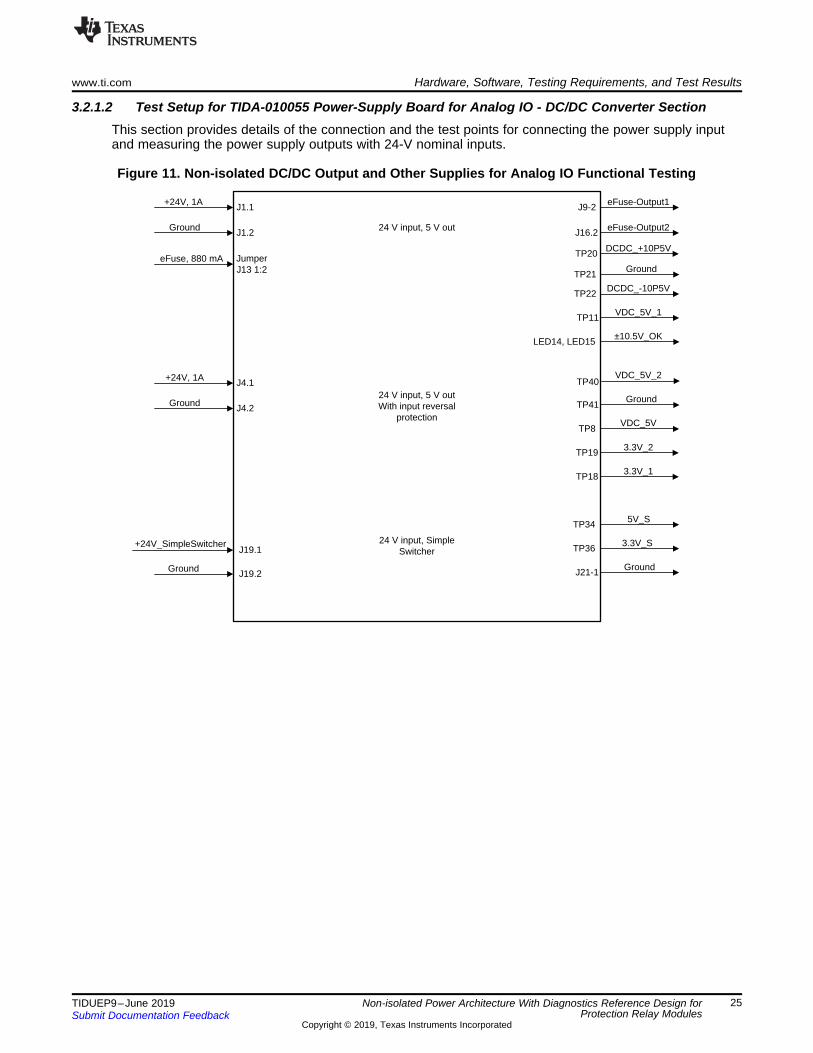
3.2.1.2 Test Setup for TIDA-010055 Power-Supply Board for Analog IO - DC/DC Converter SectionThis section provides details of the connection and the test points for connecting the power supply inputand measuring the power supply outputs with 24-V nominal inputs.
Figure 11. Non-isolated DC/DC Output and Other Supplies for Analog IO Functional Testing

24 V input, 5 V out
24 V input, 5 V outWith input reversal
protection
24 V input, SimpleSwitcher
J1.1
J1.2
J9-2
J16.2
TP20
eFuse-Output1
Ground
Ground
J4.1
J4.2
+24V, 1A
Ground
TP21
TP22
TP11
LED14, LED15
TP40
TP41
TP8
TP19
TP18
TP34
J21-1
+24V_SimpleSwitcherJ19.1 TP36
3.3V_1
5V_S
Ground
3.3V_S
JumperJ13 1:2
eFuse, 880 mA
J19.2
+24V, 1A
Ground
eFuse-Output2
DCDC_+10P5V
DCDC_-10P5V
VDC_5V_1
±10.5V_OK
VDC_5V_2
Ground
VDC_5V
3.3V_2
Hardware, Software, Testing Requirements, and Test Results www.ti.com
26 TIDUEP9–June 2019Submit Documentation Feedback
Copyright © 2019, Texas Instruments Incorporated
Non-isolated Power Architecture With Diagnostics Reference Design forProtection Relay Modules
3.2.1.3 Test Setup for TIDA-010055 Power-Supply Board for Analog IO - Power Module SectionThis section provides details of the connection and the test points for connecting the power supply inputand measuring the power supply outputs with 24-V nominal inputs.
Figure 12. Supply Rails Generated Using 5-V and 12-V Input
24 V input
24 V input
J2.1
J2.2, TP2, TP5, TP8, TP11, TP12
TP10
TP1
TP3
24V_DCI
VOUT_DCDC_P
Ground
J5.2
J5.1, TP31, TP34, TP39TP23, TP21, TP45, TP25
+24V, 1A
Ground
TP7
TP9
TP13
TP38
TP15
TP46
+24V, 2A
VCC_P_3.3
+5V_P
5V_S
VO1_5V
LMR1_PG
VO3_1.5V
VO4_3.3V
TP49 2.5V
C68
LED_D3
TP29
5V_LMR
24V/150mATP33
TP26
TP41
TP24
TP20
TP22
LMR_PG
3.3V/2A
+3.3Vsec
+3.3V
VO2_3.3V
1.2V
2.5V
TP44 1.5V
www.ti.com Hardware, Software, Testing Requirements, and Test Results
27TIDUEP9–June 2019Submit Documentation Feedback
Copyright © 2019, Texas Instruments Incorporated
Non-isolated Power Architecture With Diagnostics Reference Design forProtection Relay Modules
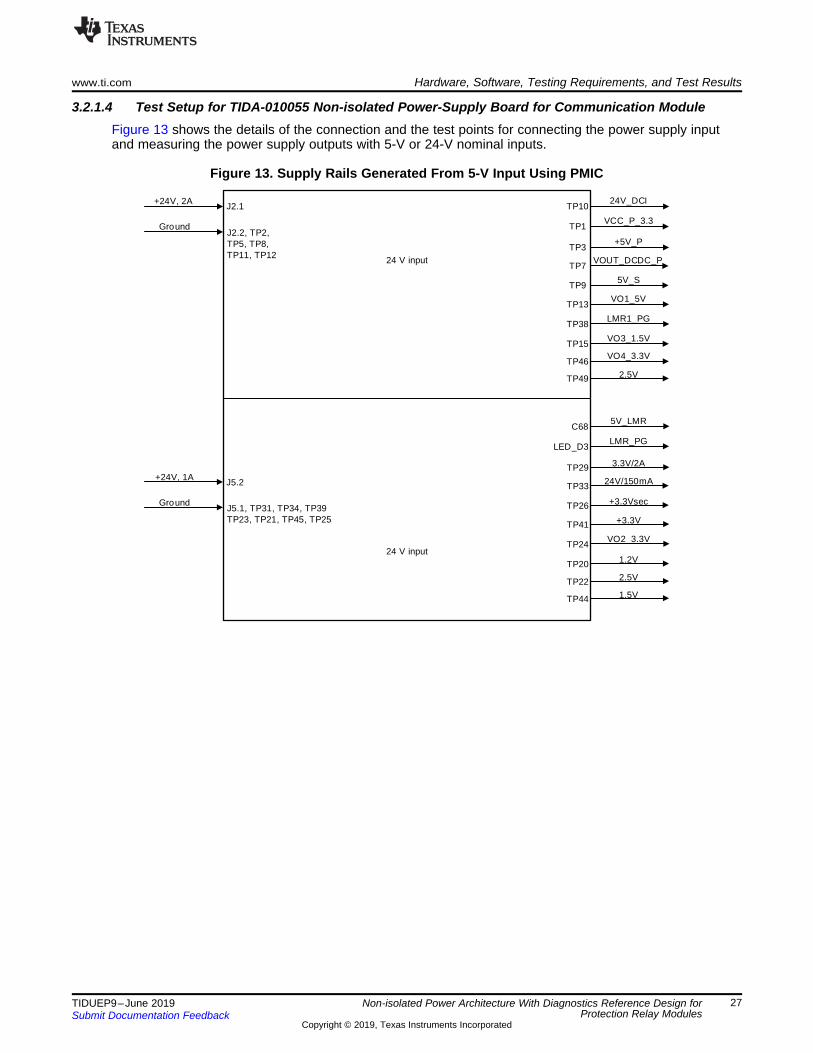
3.2.1.4 Test Setup for TIDA-010055 Non-isolated Power-Supply Board for Communication ModuleFigure 13 shows the details of the connection and the test points for connecting the power supply inputand measuring the power supply outputs with 5-V or 24-V nominal inputs.
Figure 13. Supply Rails Generated From 5-V Input Using PMIC

Hardware, Software, Testing Requirements, and Test Results www.ti.com
28 TIDUEP9–June 2019Submit Documentation Feedback
Copyright © 2019, Texas Instruments Incorporated
Non-isolated Power Architecture With Diagnostics Reference Design forProtection Relay Modules
3.2.2 Functional TestingThis section provides details of the functional tests done using the TIDA-010055 and observations.
3.2.2.1 24-V DC InputThis section provides details of the tests done and the test observations for the split-rail power suppliesgenerated using DC/DC from 24-V or 5-V input.
Table 7. Non-isolated Power Supply Board for Analog IO Measurements for DC/DC
SUPPLY INPUT INPUT CONNECTOR ANDFUNCTION
OUTPUT (V) MEASURED (V)
5-V DC input J1-1: Input TP43: 5 V 4.996J1-2: Ground J6-1: Ground
24-V input DC/DC J4-1: input TP24, J6-2: 5 V 5.126J4-2: Ground J6-1: Ground
TP1: 14 V 14.8TP2: –14 V –14.91TP29: 12 V 12.08TP31: –12 V –12.28
R23: LDO 5 V 5.11R40: LDO-5 V –4.996
TP6: REF_2.5 V_A 2.501TP5: REF_2.5 V 2.494
TP49: +3.3 V 3.288TP38: POR_Out OK
TP48: POR_Output OKTP46: Volt_Detect_Out OK
TP10: WDT input TP9: WDT_Out OKTP7: Temp_Out OK
TP45: Temp_Out1 OK
www.ti.com Hardware, Software, Testing Requirements, and Test Results
29TIDUEP9–June 2019Submit Documentation Feedback
Copyright © 2019, Texas Instruments Incorporated
Non-isolated Power Architecture With Diagnostics Reference Design forProtection Relay Modules
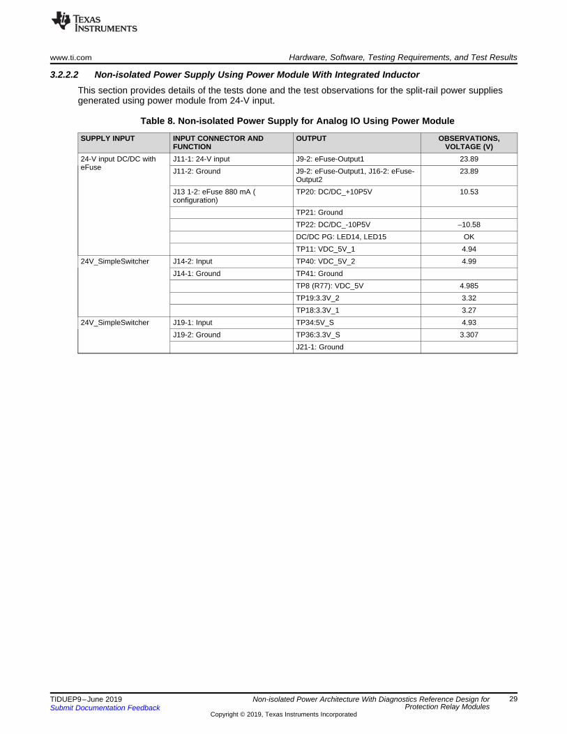
3.2.2.2 Non-isolated Power Supply Using Power Module With Integrated InductorThis section provides details of the tests done and the test observations for the split-rail power suppliesgenerated using power module from 24-V input.
Table 8. Non-isolated Power Supply for Analog IO Using Power Module
SUPPLY INPUT INPUT CONNECTOR ANDFUNCTION
OUTPUT OBSERVATIONS,VOLTAGE (V)
24-V input DC/DC witheFuse
J11-1: 24-V input J9-2: eFuse-Output1 23.89J11-2: Ground J9-2: eFuse-Output1, J16-2: eFuse-
Output223.89
J13 1-2: eFuse 880 mA (configuration)
TP20: DC/DC_+10P5V 10.53
TP21: GroundTP22: DC/DC_-10P5V –10.58DC/DC PG: LED14, LED15 OKTP11: VDC_5V_1 4.94
24V_SimpleSwitcher J14-2: Input TP40: VDC_5V_2 4.99J14-1: Ground TP41: Ground
TP8 (R77): VDC_5V 4.985TP19:3.3V_2 3.32TP18:3.3V_1 3.27
24V_SimpleSwitcher J19-1: Input TP34:5V_S 4.93J19-2: Ground TP36:3.3V_S 3.307
J21-1: Ground
Hardware, Software, Testing Requirements, and Test Results www.ti.com
30 TIDUEP9–June 2019Submit Documentation Feedback
Copyright © 2019, Texas Instruments Incorporated
Non-isolated Power Architecture With Diagnostics Reference Design forProtection Relay Modules
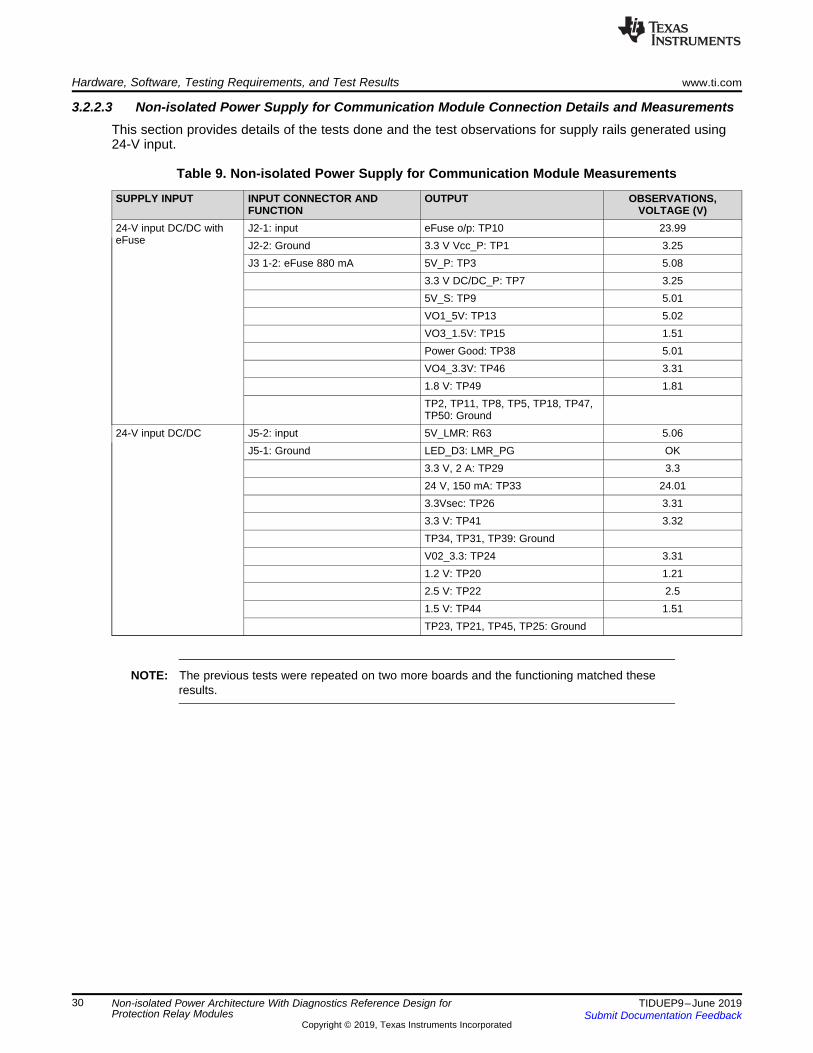
3.2.2.3 Non-isolated Power Supply for Communication Module Connection Details and MeasurementsThis section provides details of the tests done and the test observations for supply rails generated using24-V input.
Table 9. Non-isolated Power Supply for Communication Module Measurements
SUPPLY INPUT INPUT CONNECTOR ANDFUNCTION
OUTPUT OBSERVATIONS,VOLTAGE (V)
24-V input DC/DC witheFuse
J2-1: input eFuse o/p: TP10 23.99J2-2: Ground 3.3 V Vcc_P: TP1 3.25J3 1-2: eFuse 880 mA 5V_P: TP3 5.08
3.3 V DC/DC_P: TP7 3.255V_S: TP9 5.01VO1_5V: TP13 5.02VO3_1.5V: TP15 1.51Power Good: TP38 5.01VO4_3.3V: TP46 3.311.8 V: TP49 1.81TP2, TP11, TP8, TP5, TP18, TP47,TP50: Ground
24-V input DC/DC J5-2: input 5V_LMR: R63 5.06J5-1: Ground LED_D3: LMR_PG OK
3.3 V, 2 A: TP29 3.324 V, 150 mA: TP33 24.013.3Vsec: TP26 3.313.3 V: TP41 3.32TP34, TP31, TP39: GroundV02_3.3: TP24 3.311.2 V: TP20 1.212.5 V: TP22 2.51.5 V: TP44 1.51TP23, TP21, TP45, TP25: Ground
NOTE: The previous tests were repeated on two more boards and the functioning matched theseresults.
www.ti.com Hardware, Software, Testing Requirements, and Test Results
31TIDUEP9–June 2019Submit Documentation Feedback
Copyright © 2019, Texas Instruments Incorporated
Non-isolated Power Architecture With Diagnostics Reference Design forProtection Relay Modules
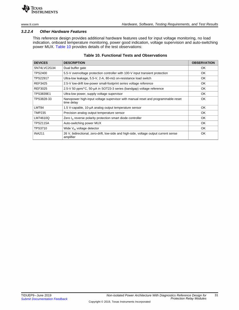
3.2.2.4 Other Hardware FeaturesThis reference design provides additional hardware features used for input voltage monitoring, no loadindication, onboard temperature monitoring, power good indication, voltage supervision and auto-switchingpower MUX. Table 10 provides details of the test observations:
Table 10. Functional Tests and Observations
DEVICES DESCRIPTION OBSERVATIONSN74LVC2G34 Dual buffer gate OKTPS2400 5.5-V overvoltage protection controller with 100-V input transient protection OKTPS22917 Ultra-low leakage, 5.5-V, 2-A, 80-mΩ on-resistance load switch OKREF3425 2.5-V low-drift low-power small-footprint series voltage reference OKREF3025 2.5-V 50 ppm/°C, 50-µA in SOT23-3 series (bandgap) voltage reference OKTPS3839E1 Ultra-low power, supply voltage supervisor OKTPS3828-33 Nanopower high-input voltage supervisor with manual reset and programmable-reset
time delayOK
LMT84 1.5 V-capable, 10-µA analog output temperature sensor OKTMP235 Precision analog output temperature sensor OKLM74610Q Zero IQ reverse polarity protection smart diode controller OKTPS2115A Auto-switching power MUX OKTPS3710 Wide VIN voltage detector OKINA211 26 V, bidirectional, zero-drift, low-side and high-side, voltage output current sense
amplifierOK

Hardware, Software, Testing Requirements, and Test Results www.ti.com
32 TIDUEP9–June 2019Submit Documentation Feedback
Copyright © 2019, Texas Instruments Incorporated
Non-isolated Power Architecture With Diagnostics Reference Design forProtection Relay Modules
3.3 Performance TestingThis section provides details of the performance tests including EMI tests that have been performed usingTIDA-010055 reference design.
3.3.1 EMI Test Setup for Testing TIDA-010055 Power-Supply Board for Communication ModuleFigure 14 shows the radiated emission setup for the reference design with an antenna at 3 M distanceplaced in a semi-anechoic chamber.
Figure 14. Three-Meter TIDA-010055 Communication RE Board Placement

www.ti.com Hardware, Software, Testing Requirements, and Test Results
33TIDUEP9–June 2019Submit Documentation Feedback
Copyright © 2019, Texas Instruments Incorporated
Non-isolated Power Architecture With Diagnostics Reference Design forProtection Relay Modules
3.3.2 EMI Performance of DC/DC Converters With 24-V Input Connected to J2The radiated emission for DC/DC converter is tested with the following configuration and 24-V input:• TPS26624, 24-V DC input with up to 800-mA output load current• LM5017, configured for 3.3-V output with 350-mA load current• TPS54202, configured for 5-V output with 400-mA load current• LM5165, configured for 3.3-V output with 150-mA load current• TPS560430, configured for 5-V output with 400-mA load current• LMR36006 configured for 5-V output• TPS62821, configured for 1.5-V output with 250-mA load current• TLV62084, configured for 1.8-V output with 250-mA load current• SN74LVC1G07, used for buffering power good output for diagnostics
Figure 15 shows the radiated emission plot.
Figure 15. TIDA-010055 J2 RE ClassB
3.3.3 EMI Performance of DC/DC Converters With 24-V Input Connected to J5The radiated emission for supply rails using a DC/DC converter is tested with the following configuration:• LMR33630, configured for 5-V output• TLV62569, configured for 5-V output with 400-mA load current• TPS560200, configured for 3.3-V output with 300-mA load current• TPS561201, configured for 3.3-V output with 300-mA load current• SN74LVC1G17, used for buffering power good output for diagnostics• TPS54331, configured for 5-V output• TLV62080, configured for 1.2-V output with 500-mA load current• TPS82672, configured for 1.5-V output with 300-mA load current• TPS73801, configured for 2.5-V output with 500-mA load current

Hardware, Software, Testing Requirements, and Test Results www.ti.com
34 TIDUEP9–June 2019Submit Documentation Feedback
Copyright © 2019, Texas Instruments Incorporated
Non-isolated Power Architecture With Diagnostics Reference Design forProtection Relay Modules
Figure 16 shows the radiated emission plot.
Figure 16. DC/DC Buck Power Module Radiated Emission J2 ClassB
3.3.4 Power-Supply Board for Analog IO EMI Performance Testing With 24-V Input Connected to J11The radiated emission for supply rails using the power module and DC/DC converters is tested with thefollowing configuration:• TPS26624, eFuse configured for 800-mA output with 300-mA load• LMZM23600, configured in inverted buck configuration for ±10.5-V output with 250-mA load• LM76002, configured for 5-V output with 300-mA load• SN74LVC2G34, used for buffering power good output for diagnostics
Figure 17 shows the radiated emission plot.
Figure 17. DC/DC, 12-V, 5-V Buck Power Module Radiated Emission

TIDA ± 010055 Communication Module Power Supply Board
TIDA ± 010055 AFE Power Supply Board
TIDA ± 00227Compact NX5
EFT Generator
LoadDC Output
AC Input240 V
240 V + EFT(1 KV ± 2.5 KV)
DC Output
www.ti.com Hardware, Software, Testing Requirements, and Test Results
35TIDUEP9–June 2019Submit Documentation Feedback
Copyright © 2019, Texas Instruments Incorporated
Non-isolated Power Architecture With Diagnostics Reference Design forProtection Relay Modules
3.3.5 EFT and Surge Test Setup, TIDA-010055 Boards Test Method, Acceptance Criteria, and ResultsEFT and Surge testing was done on the TIDA-010055 boards with the following test conditions:• 240-V AC supply connected to TIDA-00227 and TIDA-00227 reference design power supply output
connected to the TIDA-010055 non-isolated power supply board for communication module and surgewith 2 Ω applied
• 240-V AC supply connected to TIDA-00227 and TIDA-00227 reference design power supply outputconnected to the TIDA-01055 non-isolated power supply board for analog IO module and surge with 2Ω applied
• Surge with 42-Ω impedance and EFT applied on 24-V DC auxiliary supply
Figure 18 shows the setup for testing EFT:
Figure 18. Setup for EFT Testing
Figure 19 shows the TIDA-010055 power supply board for communication module interfaced to theTIDA-00227 reference design.
Figure 19. TIDA-010055 Supply for Communication Module Board Connected to TIDA-00227 for Testing

Hardware, Software, Testing Requirements, and Test Results www.ti.com
36 TIDUEP9–June 2019Submit Documentation Feedback
Copyright © 2019, Texas Instruments Incorporated
Non-isolated Power Architecture With Diagnostics Reference Design forProtection Relay Modules
Testing EMC With TI Design Board TIDA-00227 Connected at the InputTable 11 summarizes surge and EFT test results for TIDA-010055 communication board connected to the output of TIDA-00227 power supply with240-V AC input.
Table 11. Results for Non-isolated Power Supply Board for Communication Module Connected to TIDA-00227TEST TYPE AND STANDARD TRANSIENT VOLTAGE AMPLITUDE MEASUREMENT BEFORE TEST RESULT AFTER TEST
EFT IEC61000-4-4 ±1 kV, 5 kHz, 100 kHz for 1 minute J2 – 24-V input, TP3: 5.08, J6 – 24-V input5V_LMR:5.06 J2 – 24-V input, TP3: 5.08, J6 – 24-V input 5V_LMR:5.06
EFT IEC61000-4-4 ±2 kV, 5 kHz, 100 kHz for 1 minute J2 – 24-V input, TP3: 5.08, J6 – 24-V input5V_LMR:5.06 J2 – 24-V input, TP3: 5.08, J6 – 24-V input 5V_LMR:5.06
EFT IEC61000-4-4 ±2.5 kV, 5 kHz, 100 kHz for 1 minute J2 – 24-V input, TP3: 5.08, J6 – 24-V input5V_LMR:5.06 J2 – 24-V input, TP3: 5.08, J6 – 24-V input 5V_LMR:5.06
Surge, IEC61000-4-5 ±1 kV, 2 Ω, 5 pulses J2 – 24-V input, TP3: 5.08, J6 – 24-V input5V_LMR:5.06 J2 – 24-V input, TP3: 5.08, J6 – 24-V input 5V_LMR:5.06
Surge, IEC61000-4-5 ±2 kV, 2 Ω, 5 pulses J2 – 24-V input, TP3: 5.08, J6 – 24-V input5V_LMR:5.06 J2 – 24-V input, TP3: 5.08, J6 – 24-V input 5V_LMR:5.06
Surge, IEC61000-4-5 ±2.5 kV, 2 Ω, 5 pulses J2 – 24-V input, TP3: 5.08, J6 – 24-V input5V_LMR:5.06 J2 – 24-V input, TP3: 5.08, J6 – 24-V input 5V_LMR:5.06
Table 12 summarizes surge and EFT test results for the TIDA-010055 power supply board for analog IO module connected to the output of TIDA-00227 power supply with 240-V AC input.
Table 12. Results for Non-isolated Power-Supply Board for Analog IO Module Connected to TIDA-00227TEST TYPE AND
STANDARD TRANSIENT VOLTAGE AMPLITUDE MEASUREMENT BEFORE TEST RESULT AFTER TEST
EFT IEC61000-4-4 ±1 kV, 5 kHz, 100 kHz for 1 minute J4 – 24-V input, TP1:14.8V, TP2: 14.92V J11-24 V, TP20:10.53, TP22: 10.58
J4 – 24-V input, TP1:14.8V, TP2: 14.92V J11-24 V, TP20:10.53, TP22: 10.58
EFT IEC61000-4-4 ±2 kV, 5 kHz, 100 kHz for 1 minute J4 – 24-V input, TP1:14.8V, TP2: 14.92V J11-24 V, TP20:10.53, TP22: 10.58
J4 – 24-V input, TP1:14.8V, TP2: 14.92V J11-24 V, TP20:10.53, TP22: 10.58
EFT IEC61000-4-4 ±2.5 kV, 5 kHz, 100 kHz for 1 minute J4 – 24-V input, TP1:14.8V, TP2: 14.92V J11-24 V, TP20:10.53, TP22: 10.58
J4 – 24-V input, TP1:14.8V, TP2: 14.92V J11-24 V, TP20:10.53, TP22: 10.58
Surge, IEC61000-4-5 ±1 kV, 2Ω, 5 pulses J4 – 24-V input, TP1:14.8V, TP2: 14.92V J11-24 V, TP20:10.53, TP22: 10.58
J4 – 24-V input, TP1:14.8V, TP2: 14.92V J11-24 V, TP20:10.53, TP22: 10.58
Surge, IEC61000-4-5 ±2 kV, 2Ω, 5 pulses J4 – 24-V input, TP1:14.8V, TP2: 14.92V J11-24 V, TP20:10.53, TP22: 10.58
J4 – 24-V input, TP1:14.8V, TP2: 14.92V J11-24 V, TP20:10.53, TP22: 10.58
Surge, IEC61000-4-5 ±2.5 kV, 2Ω, 5 pulses J4 – 24-V input, TP1:14.8V, TP2: 14.92V J11-24 V, TP20:10.53, TP22: 10.58
J4 – 24-V input, TP1:14.8V, TP2: 14.92V J11-24 V, TP20:10.53, TP22: 10.58
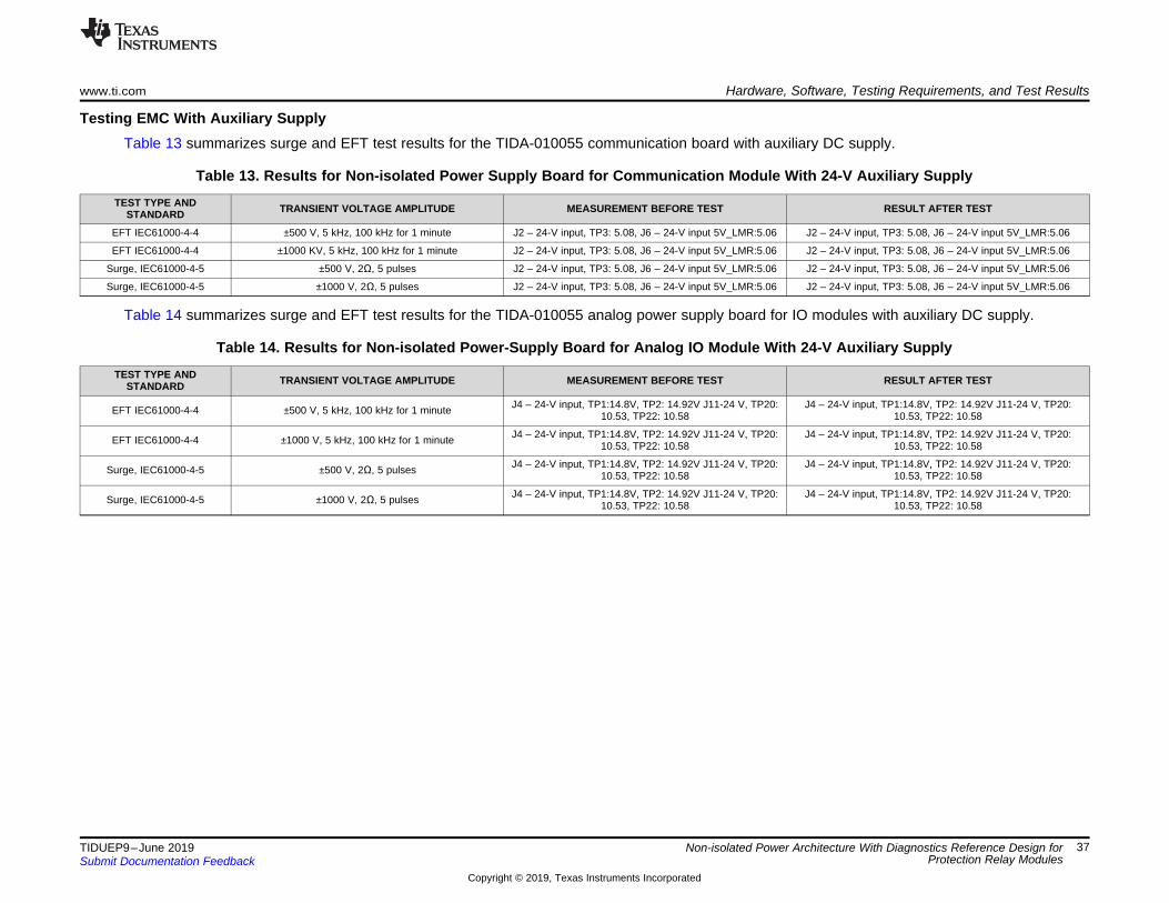
www.ti.com Hardware, Software, Testing Requirements, and Test Results
37TIDUEP9–June 2019Submit Documentation Feedback
Copyright © 2019, Texas Instruments Incorporated
Non-isolated Power Architecture With Diagnostics Reference Design forProtection Relay Modules
Testing EMC With Auxiliary SupplyTable 13 summarizes surge and EFT test results for the TIDA-010055 communication board with auxiliary DC supply.
Table 13. Results for Non-isolated Power Supply Board for Communication Module With 24-V Auxiliary SupplyTEST TYPE AND
STANDARD TRANSIENT VOLTAGE AMPLITUDE MEASUREMENT BEFORE TEST RESULT AFTER TEST
EFT IEC61000-4-4 ±500 V, 5 kHz, 100 kHz for 1 minute J2 – 24-V input, TP3: 5.08, J6 – 24-V input 5V_LMR:5.06 J2 – 24-V input, TP3: 5.08, J6 – 24-V input 5V_LMR:5.06
EFT IEC61000-4-4 ±1000 KV, 5 kHz, 100 kHz for 1 minute J2 – 24-V input, TP3: 5.08, J6 – 24-V input 5V_LMR:5.06 J2 – 24-V input, TP3: 5.08, J6 – 24-V input 5V_LMR:5.06
Surge, IEC61000-4-5 ±500 V, 2Ω, 5 pulses J2 – 24-V input, TP3: 5.08, J6 – 24-V input 5V_LMR:5.06 J2 – 24-V input, TP3: 5.08, J6 – 24-V input 5V_LMR:5.06
Surge, IEC61000-4-5 ±1000 V, 2Ω, 5 pulses J2 – 24-V input, TP3: 5.08, J6 – 24-V input 5V_LMR:5.06 J2 – 24-V input, TP3: 5.08, J6 – 24-V input 5V_LMR:5.06
Table 14 summarizes surge and EFT test results for the TIDA-010055 analog power supply board for IO modules with auxiliary DC supply.
Table 14. Results for Non-isolated Power-Supply Board for Analog IO Module With 24-V Auxiliary SupplyTEST TYPE AND
STANDARD TRANSIENT VOLTAGE AMPLITUDE MEASUREMENT BEFORE TEST RESULT AFTER TEST
EFT IEC61000-4-4 ±500 V, 5 kHz, 100 kHz for 1 minute J4 – 24-V input, TP1:14.8V, TP2: 14.92V J11-24 V, TP20:10.53, TP22: 10.58
J4 – 24-V input, TP1:14.8V, TP2: 14.92V J11-24 V, TP20:10.53, TP22: 10.58
EFT IEC61000-4-4 ±1000 V, 5 kHz, 100 kHz for 1 minute J4 – 24-V input, TP1:14.8V, TP2: 14.92V J11-24 V, TP20:10.53, TP22: 10.58
J4 – 24-V input, TP1:14.8V, TP2: 14.92V J11-24 V, TP20:10.53, TP22: 10.58
Surge, IEC61000-4-5 ±500 V, 2Ω, 5 pulses J4 – 24-V input, TP1:14.8V, TP2: 14.92V J11-24 V, TP20:10.53, TP22: 10.58
J4 – 24-V input, TP1:14.8V, TP2: 14.92V J11-24 V, TP20:10.53, TP22: 10.58
Surge, IEC61000-4-5 ±1000 V, 2Ω, 5 pulses J4 – 24-V input, TP1:14.8V, TP2: 14.92V J11-24 V, TP20:10.53, TP22: 10.58
J4 – 24-V input, TP1:14.8V, TP2: 14.92V J11-24 V, TP20:10.53, TP22: 10.58
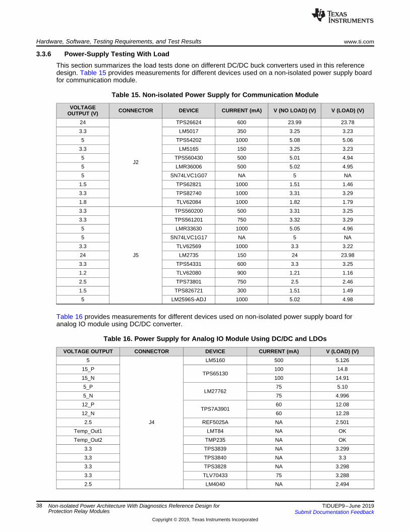
Hardware, Software, Testing Requirements, and Test Results www.ti.com
38 TIDUEP9–June 2019Submit Documentation Feedback
Copyright © 2019, Texas Instruments Incorporated
Non-isolated Power Architecture With Diagnostics Reference Design forProtection Relay Modules
3.3.6 Power-Supply Testing With LoadThis section summarizes the load tests done on different DC/DC buck converters used in this referencedesign. Table 15 provides measurements for different devices used on a non-isolated power supply boardfor communication module.
Table 15. Non-isolated Power Supply for Communication Module
VOLTAGEOUTPUT (V) CONNECTOR DEVICE CURRENT (mA) V (NO LOAD) (V) V (LOAD) (V)
24
J2
TPS26624 600 23.99 23.783.3 LM5017 350 3.25 3.235 TPS54202 1000 5.08 5.06
3.3 LM5165 150 3.25 3.235 TPS560430 500 5.01 4.945 LMR36006 500 5.02 4.955 SN74LVC1G07 NA 5 NA
1.5 TPS62821 1000 1.51 1.463.3 TPS82740 1000 3.31 3.291.8 TLV62084 1000 1.82 1.793.3
J5
TPS560200 500 3.31 3.253.3 TPS561201 750 3.32 3.295 LMR33630 1000 5.05 4.965 SN74LVC1G17 NA 5 NA
3.3 TLV62569 1000 3.3 3.2224 LM2735 150 24 23.983.3 TPS54331 600 3.3 3.251.2 TLV62080 900 1.21 1.162.5 TPS73801 750 2.5 2.461.5 TPS826721 300 1.51 1.495 LM2596S-ADJ 1000 5.02 4.98
Table 16 provides measurements for different devices used on non-isolated power supply board foranalog IO module using DC/DC converter.
Table 16. Power Supply for Analog IO Module Using DC/DC and LDOs
VOLTAGE OUTPUT CONNECTOR DEVICE CURRENT (mA) V (LOAD) (V)5
J4
LM5160 500 5.12615_P
TPS65130100 14.8
15_N 100 14.915_P
LM2776275 5.10
5_N 75 4.99612_P
TPS7A390160 12.08
12_N 60 12.282.5 REF5025A NA 2.501
Temp_Out1 LMT84 NA OKTemp_Out2 TMP235 NA OK
3.3 TPS3839 NA 3.2993,3 TPS3840 NA 3.33.3 TPS3828 NA 3.2983.3 TLV70433 75 3.2882.5 LM4040 NA 2.494
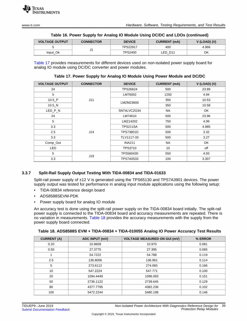
www.ti.com Hardware, Software, Testing Requirements, and Test Results
39TIDUEP9–June 2019Submit Documentation Feedback
Copyright © 2019, Texas Instruments Incorporated
Non-isolated Power Architecture With Diagnostics Reference Design forProtection Relay Modules
Table 16. Power Supply for Analog IO Module Using DC/DC and LDOs (continued)VOLTAGE OUTPUT CONNECTOR DEVICE CURRENT (mA) V (LOAD) (V)
5J1
TPS22917 400 4.966Input_Ok TPS2400 LED_D11 OK
Table 17 provides measurements for different devices used on non-isolated power supply board foranalog IO module using DC/DC converter and power modules.
Table 17. Power Supply for Analog IO Module Using Power Module and DC/DC
VOLTAGE OUTPUT CONNECTOR DEVICE CURRENT (mA) V (LOAD) (V)24
J11
TPS26624 500 23.895 LM76002 1250 4.94
10.5_PLMZM23600
350 10.5310.5_N 350 10.58
LED_P_N SN74LVC2G34 NA OK24
J14
LM74610 500 23.965 LMZ14202 750 4.99
3.3 TPS2115A 500 4.9852.5 TPS73801D 500 3.323.3 TLV1117-33 500 3.27
Comp_Out INA211 NA OKLED TPS3710 10 off
5J19
TPS560430 550 4.933.3 TPS7A0533 100 3.307
3.3.7 Split-Rail Supply Output Testing With TIDA-00834 and TIDA-01633Split-rail power supply of ±12 V is generated using the TPS65130 and TPS7A3901 devices. The powersupply output was tested for performance in analog input module applications using the following setup:• TIDA-00834 reference design board• ADS8588SEVM-PDK• Power supply board for analog IO module
An accuracy test is done using the split-rail power supply on the TIDA-00834 board initially. The split-railpower supply is connected to the TIDA-00834 board and accuracy measurements are repeated. There isno variation in measurements. Table 18 provides the accuracy measurements with the supply from thepower supply board connected.
Table 18. ADS8588S EVM + TIDA-00834 + TIDA-010055 Analog IO Power Accuracy Test Results
CURRENT (A) ADC INPUT (mV) VOLTAGE MEASURED ON GUI (mV) % ERROR0.20 10.9609 10.970 0.0810.50 27.3775 27.395 0.065
1 54.7222 54.788 0.1192.5 136.8056 136.961 0.1145 273.6112 274.065 0.16610 547.2224 547.771 0.10020 1094.4449 1096.093 0.15150 2736.1122 2739.645 0.12980 4377.7795 4382.236 0.102
100 5472.2244 5480.198 0.146
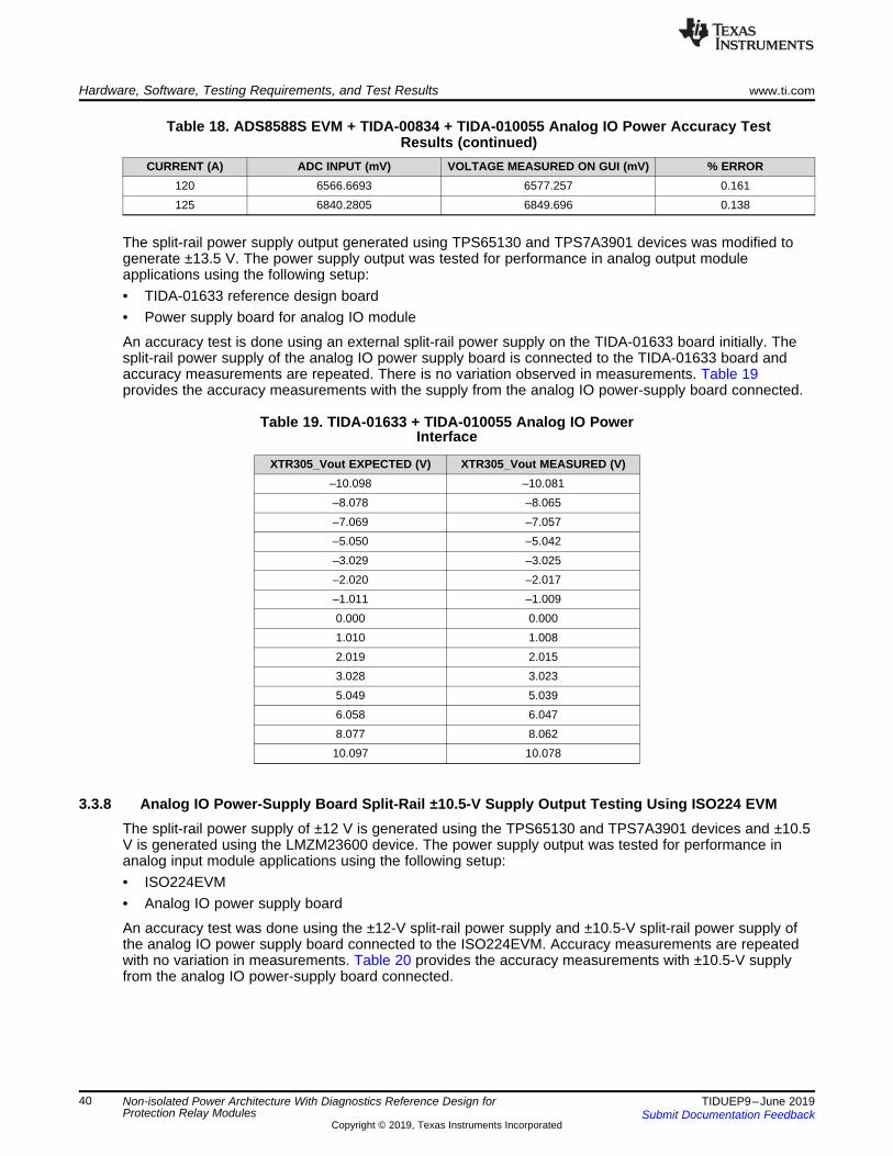
Hardware, Software, Testing Requirements, and Test Results www.ti.com
40 TIDUEP9–June 2019Submit Documentation Feedback
Copyright © 2019, Texas Instruments Incorporated
Non-isolated Power Architecture With Diagnostics Reference Design forProtection Relay Modules
Table 18. ADS8588S EVM + TIDA-00834 + TIDA-010055 Analog IO Power Accuracy TestResults (continued)
CURRENT (A) ADC INPUT (mV) VOLTAGE MEASURED ON GUI (mV) % ERROR120 6566.6693 6577.257 0.161125 6840.2805 6849.696 0.138
The split-rail power supply output generated using TPS65130 and TPS7A3901 devices was modified togenerate ±13.5 V. The power supply output was tested for performance in analog output moduleapplications using the following setup:• TIDA-01633 reference design board• Power supply board for analog IO module
An accuracy test is done using an external split-rail power supply on the TIDA-01633 board initially. Thesplit-rail power supply of the analog IO power supply board is connected to the TIDA-01633 board andaccuracy measurements are repeated. There is no variation observed in measurements. Table 19provides the accuracy measurements with the supply from the analog IO power-supply board connected.
Table 19. TIDA-01633 + TIDA-010055 Analog IO PowerInterface
XTR305_Vout EXPECTED (V) XTR305_Vout MEASURED (V)–10.098 –10.081–8.078 –8.065–7.069 –7.057–5.050 –5.042–3.029 –3.025–2.020 –2.017–1.011 –1.0090.000 0.0001.010 1.0082.019 2.0153.028 3.0235.049 5.0396.058 6.0478.077 8.06210.097 10.078
3.3.8 Analog IO Power-Supply Board Split-Rail ±10.5-V Supply Output Testing Using ISO224 EVMThe split-rail power supply of ±12 V is generated using the TPS65130 and TPS7A3901 devices and ±10.5V is generated using the LMZM23600 device. The power supply output was tested for performance inanalog input module applications using the following setup:• ISO224EVM• Analog IO power supply board
An accuracy test was done using the ±12-V split-rail power supply and ±10.5-V split-rail power supply ofthe analog IO power supply board connected to the ISO224EVM. Accuracy measurements are repeatedwith no variation in measurements. Table 20 provides the accuracy measurements with ±10.5-V supplyfrom the analog IO power-supply board connected.
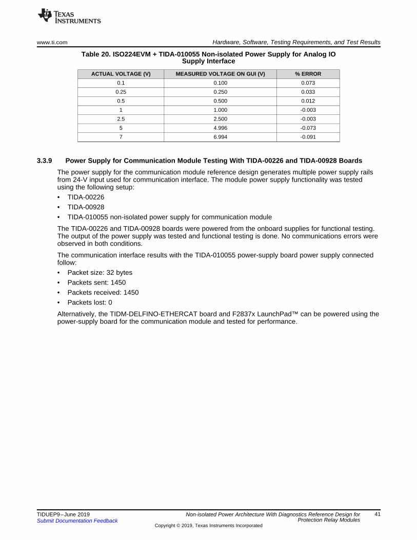
www.ti.com Hardware, Software, Testing Requirements, and Test Results
41TIDUEP9–June 2019Submit Documentation Feedback
Copyright © 2019, Texas Instruments Incorporated
Non-isolated Power Architecture With Diagnostics Reference Design forProtection Relay Modules
Table 20. ISO224EVM + TIDA-010055 Non-isolated Power Supply for Analog IOSupply Interface
ACTUAL VOLTAGE (V) MEASURED VOLTAGE ON GUI (V) % ERROR0.1 0.100 0.073
0.25 0.250 0.0330.5 0.500 0.0121 1.000 -0.003
2.5 2.500 -0.0035 4.996 -0.0737 6.994 -0.091
3.3.9 Power Supply for Communication Module Testing With TIDA-00226 and TIDA-00928 BoardsThe power supply for the communication module reference design generates multiple power supply railsfrom 24-V input used for communication interface. The module power supply functionality was testedusing the following setup:• TIDA-00226• TIDA-00928• TIDA-010055 non-isolated power supply for communication module
The TIDA-00226 and TIDA-00928 boards were powered from the onboard supplies for functional testing.The output of the power supply was tested and functional testing is done. No communications errors wereobserved in both conditions.
The communication interface results with the TIDA-010055 power-supply board power supply connectedfollow:• Packet size: 32 bytes• Packets sent: 1450• Packets received: 1450• Packets lost: 0
Alternatively, the TIDM-DELFINO-ETHERCAT board and F2837x LaunchPad™ can be powered using thepower-supply board for the communication module and tested for performance.
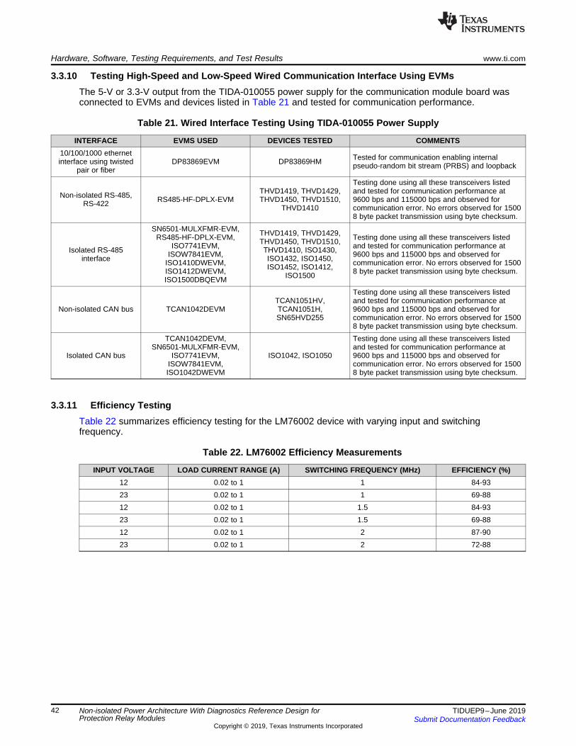
Hardware, Software, Testing Requirements, and Test Results www.ti.com
42 TIDUEP9–June 2019Submit Documentation Feedback
Copyright © 2019, Texas Instruments Incorporated
Non-isolated Power Architecture With Diagnostics Reference Design forProtection Relay Modules
3.3.10 Testing High-Speed and Low-Speed Wired Communication Interface Using EVMsThe 5-V or 3.3-V output from the TIDA-010055 power supply for the communication module board wasconnected to EVMs and devices listed in Table 21 and tested for communication performance.
Table 21. Wired Interface Testing Using TIDA-010055 Power Supply
INTERFACE EVMS USED DEVICES TESTED COMMENTS10/100/1000 ethernetinterface using twisted
pair or fiberDP83869EVM DP83869HM Tested for communication enabling internal
pseudo-random bit stream (PRBS) and loopback
Non-isolated RS-485,RS-422 RS485-HF-DPLX-EVM
THVD1419, THVD1429,THVD1450, THVD1510,
THVD1410
Testing done using all these transceivers listedand tested for communication performance at9600 bps and 115000 bps and observed forcommunication error. No errors observed for 15008 byte packet transmission using byte checksum.
Isolated RS-485interface
SN6501-MULXFMR-EVM,RS485-HF-DPLX-EVM,
ISO7741EVM,ISOW7841EVM,
ISO1410DWEVM,ISO1412DWEVM,ISO1500DBQEVM
THVD1419, THVD1429,THVD1450, THVD1510,THVD1410, ISO1430,ISO1432, ISO1450,ISO1452, ISO1412,
ISO1500
Testing done using all these transceivers listedand tested for communication performance at9600 bps and 115000 bps and observed forcommunication error. No errors observed for 15008 byte packet transmission using byte checksum.
Non-isolated CAN bus TCAN1042DEVMTCAN1051HV,TCAN1051H,SN65HVD255
Testing done using all these transceivers listedand tested for communication performance at9600 bps and 115000 bps and observed forcommunication error. No errors observed for 15008 byte packet transmission using byte checksum.
Isolated CAN bus
TCAN1042DEVM,SN6501-MULXFMR-EVM,
ISO7741EVM,ISOW7841EVM,ISO1042DWEVM
ISO1042, ISO1050
Testing done using all these transceivers listedand tested for communication performance at9600 bps and 115000 bps and observed forcommunication error. No errors observed for 15008 byte packet transmission using byte checksum.
3.3.11 Efficiency TestingTable 22 summarizes efficiency testing for the LM76002 device with varying input and switchingfrequency.
Table 22. LM76002 Efficiency Measurements
INPUT VOLTAGE LOAD CURRENT RANGE (A) SWITCHING FREQUENCY (MHz) EFFICIENCY (%)12 0.02 to 1 1 84-9323 0.02 to 1 1 69-8812 0.02 to 1 1.5 84-9323 0.02 to 1 1.5 69-8812 0.02 to 1 2 87-9023 0.02 to 1 2 72-88

www.ti.com Hardware, Software, Testing Requirements, and Test Results
43TIDUEP9–June 2019Submit Documentation Feedback
Copyright © 2019, Texas Instruments Incorporated
Non-isolated Power Architecture With Diagnostics Reference Design forProtection Relay Modules
3.4 Power Supply Related Reference Designs for Protection Relay ModulesThe reference designs in Table 23 can be used to design power architecture for modular protection relayswith plugable modules, multifunction relay, terminal unit and other grid end equipment requiring widesupply input operation, isolated or non-isolated power rails output with high efficiency, optimized size, andcost.
Table 23. Power Architecture Focused Reference Design
REFERENCE DESIGN FOCUS MODULE DESCRIPTION
TIDA-00127 Auxiliary power supplymodule
Wide input AC/DC power supply with supply override time of 50 ms ormore and 30-W output
TIDA-00227 Auxiliary power supplymodule
Wide input AC/DC power supply with supply override time of 50 ms ormore and 12W output
TIDA-00300AC analog input module,Communication module, DCanalog input/output module
Isolated power supply using DC/DC converter with integrated FET,DC/DC power module, Fly-Buck™ DC-DC converter and Transformerdriver for analog input/output, binary input and communication module
TIDA-010055AC analog input module,Communication module, DCanalog input/output module
Non Isolated power supply using DC-DC converter with integrated FET,DC/DC with integrated inductor, DC/DC in HotRod™ package for analoginput/output, binary input and communication module
TIDA-010011 Processor module
Non-isolated power supply architecture using DC/DC converter withintegrated FET/ DC/DC with integrated inductor, Power managementIntegrated circuit PMIC, DC/DC in HotRod™ package for processormodule with high efficiency and fast load transient response
TIDA-01027 Processor and dataacquisition module Low-noise power supply for data acquisition systems
3.5 Summary of Test ResultsTable 24 summarizes the tests performed on this design and the resulting observations.
Table 24. Summary and Observations of the Tests Performed
SERIAL NUMBER PARAMETERS OBSERVATIONS1 5 V from 24-V input using wide input DC/DC OK2 5-V output after load switch with input OK indication OK3 Split-rail DC/DC converter output with 5-V input OK4 LDO to generate ±12 V and ±5 V and 3.3 V OK5 Voltage reference outputs OK6 Analog temperature sensor outputs OK7 ±10.5-V output from DC/DC power module configured for inverted buck with LED
indicationOK
8 24-V to 5-V synchronous buck converter OK9 24-V to 5.5-V SIMPLE SWITCHER, 2 A with input reversal protection and SIMPLE
SWITCHER with 0.6 A and 3.3-V LDO outputOK
10 Power MUX, no load indication and 1-A LDO outputs OK11 eFuse and synchronous buck converter outputs OK12 Synchronous buck converter outputs with low EMI OK13 LM2596 and LP87322 EVM interface OK14 DC/DC converter with HotRod package OK15 Step-down converter with Eco-mode outputs OK16 Pre-compliance EMI and EMC testing as per CISPR22 and IEC61000-4-4, IEC61000-
4-5OK

Design Files www.ti.com
44 TIDUEP9–June 2019Submit Documentation Feedback
Copyright © 2019, Texas Instruments Incorporated
Non-isolated Power Architecture With Diagnostics Reference Design forProtection Relay Modules
4 Design Files
4.1 SchematicsTo download the schematics for each board, see the design files at TIDA-0010055.
4.2 Bill of MaterialsTo download the bill of materials (BOM) for each board, see the design files at TIDA-010055.
4.3 PCB Layout RecommendationsTo download the layout prints for each board, see the design files at TIDA-010055.
4.4 Altium ProjectTo download the Altium Designer® project files for each board, see the design files at TIDA-0010055.
4.5 Gerber FilesTo download the Gerber files for each board, see the design files at TIDA-010055.
4.6 Assembly DrawingsTo download the assembly drawings for each board, see the design files at TIDA-0010055.
5 Related DocumentationThe below is list of documents that can be referenced during design of power supplies for communicationand analog IO modules• Texas Instruments, Power Management Guide 2018 Marketing Selection Guide• Texas Instruments, A Topical Index of TI LDO Application Notes• Texas Instruments, TI Power Solutions. DC/DC Converter Modules for Space-Constrained Applications
Marketing Selection Guide• Texas Instruments, Inverting Application for the LMZM23601 and LMZM23600 Application Report• Texas Instruments, EMI Mitigation Techniques Using the LMZM23601 Application Report
5.1 TrademarksHotRod, Eco-mode, MicroSIP, Fly-Buck, FemtoFET, NexFET, DCS-Control, MicroSiP, LaunchPad aretrademarks of Texas Instruments.SIMPLE SWITCHER is a registered trademark of Texas Instruments.Altium Designer is a registered trademark of Altium LLC or its affiliated companies.Arm, Cortex are registered trademarks of Arm Limited.All other trademarks are the property of their respective owners.
5.2 Third-Party Products DisclaimerTI'S PUBLICATION OF INFORMATION REGARDING THIRD-PARTY PRODUCTS OR SERVICES DOESNOT CONSTITUTE AN ENDORSEMENT REGARDING THE SUITABILITY OF SUCH PRODUCTS ORSERVICES OR A WARRANTY, REPRESENTATION OR ENDORSEMENT OF SUCH PRODUCTS ORSERVICES, EITHER ALONE OR IN COMBINATION WITH ANY TI PRODUCT OR SERVICE.
www.ti.com Terminology
45TIDUEP9–June 2019Submit Documentation Feedback
Copyright © 2019, Texas Instruments Incorporated
Non-isolated Power Architecture With Diagnostics Reference Design forProtection Relay Modules
6 TerminologyI/O — Input or Output
EMI — Electro Magnetic Interference
POL — Point of Load
AFE —Analog Front End
7 About the AuthorsKALLIKUPPA MUNIYAPPA SREENIVASA is a systems architect at Texas Instruments where he isresponsible for developing reference design solutions for the industrial segment. Sreenivasa brings to thisrole his experience in high-speed digital and analog systems design. Sreenivasa earned his bachelor ofengineering (BE) in electronics and communication engineering (BE-E&C) from VTU, Mysore, India.
AMIT KUMBASI is a systems architect at Texas Instruments Dallas where he is responsible fordeveloping subsystem solutions for Grid Infrastructure within Industrial Systems. Amit brings to this rolehis expertise with defining products, business development, and board-level design using precision analogand mixed-signal devices. He holds a master’s in ECE (Texas Tech) and an MBA (University of Arizona).

IMPORTANT NOTICE AND DISCLAIMER
TI PROVIDES TECHNICAL AND RELIABILITY DATA (INCLUDING DATASHEETS), DESIGN RESOURCES (INCLUDING REFERENCEDESIGNS), APPLICATION OR OTHER DESIGN ADVICE, WEB TOOLS, SAFETY INFORMATION, AND OTHER RESOURCES “AS IS”AND WITH ALL FAULTS, AND DISCLAIMS ALL WARRANTIES, EXPRESS AND IMPLIED, INCLUDING WITHOUT LIMITATION ANYIMPLIED WARRANTIES OF MERCHANTABILITY, FITNESS FOR A PARTICULAR PURPOSE OR NON-INFRINGEMENT OF THIRDPARTY INTELLECTUAL PROPERTY RIGHTS.These resources are intended for skilled developers designing with TI products. You are solely responsible for (1) selecting the appropriateTI products for your application, (2) designing, validating and testing your application, and (3) ensuring your application meets applicablestandards, and any other safety, security, or other requirements. These resources are subject to change without notice. TI grants youpermission to use these resources only for development of an application that uses the TI products described in the resource. Otherreproduction and display of these resources is prohibited. No license is granted to any other TI intellectual property right or to any thirdparty intellectual property right. TI disclaims responsibility for, and you will fully indemnify TI and its representatives against, any claims,damages, costs, losses, and liabilities arising out of your use of these resources.TI’s products are provided subject to TI’s Terms of Sale (www.ti.com/legal/termsofsale.html) or other applicable terms available either onti.com or provided in conjunction with such TI products. TI’s provision of these resources does not expand or otherwise alter TI’s applicablewarranties or warranty disclaimers for TI products.
Mailing Address: Texas Instruments, Post Office Box 655303, Dallas, Texas 75265Copyright © 2019, Texas Instruments Incorporated