Nikkon Ghosh Dissertation Submitted to the Faculty of...
167
MONOLITHIC MULTIFINGER LATERAL NANODIAMOND ELECTRON EMISSION DEVICES By Nikkon Ghosh Dissertation Submitted to the Faculty of the Graduate School of Vanderbilt University in partial fulfillment of the requirements for the degree of DOCTOR OF PHILOSOPHY in Electrical Engineering December, 2012 Nashville, Tennessee Approved: Professor Weng P. Kang (Chair) Professor Jim L. Davidson Professor Bharat L. Bhuva Professor Yaqiong Xu Professor Deyu Li
-
Upload
duongkhuong -
Category
Documents
-
view
221 -
download
2
Transcript of Nikkon Ghosh Dissertation Submitted to the Faculty of...

MONOLITHIC MULTIFINGER LATERAL NANODIAMOND ELECTRON
EMISSION DEVICES
By
Nikkon Ghosh
Dissertation
Submitted to the Faculty of the
Graduate School of Vanderbilt University
in partial fulfillment of the requirements
for the degree of
DOCTOR OF PHILOSOPHY
in
Electrical Engineering
December, 2012
Nashville, Tennessee
Approved:
Professor Weng P. Kang (Chair)
Professor Jim L. Davidson
Professor Bharat L. Bhuva
Professor Yaqiong Xu
Professor Deyu Li
ii
To my dearest wife,
&
To my beloved parents and sister

iii
ACKNOWLEDGMENTS
I am deeply thankful to my dissertation advisor, Prof. Weng Poo Kang for
offering me the opportunity to work on this research, and continuously guiding me
through the course of my graduate study. His technical inputs helped me to clearly
understand the objectives of the research and develop problem-solving skills on more
than one occasions. He has expertly guided my growth in this field of research and
beyond and set targets for me to accomplish, which galvanized me to improve my
thought process and work attitude. I express my heartfelt gratitude to Prof. Jim L.
Davidson for his always prompt and sound technical assistance, constant encouragement
and camaraderie. He has played a great role in defining and widening the scope of this
research, in the process setting up exciting objectives to focus on during the progress of
my work. I would also like to thank Prof. Bharat L. Bhuva, Prof. Deyu Li and Prof.
Yaqiong Xu for serving on my Ph.D. committee. Their valuable technical suggestions
were instrumental in giving a well-defined shape to this research work. I am thankful to
all my present and ex-colleagues of the Diamond Microelectronics Research Group,
especially Dr. Supil Raina, Mr. Mick Howell, Mr. Shao-Hua Hsu, Dr. Bo K. Choi, Dr.
Karthik Subramanian, Dr. Yong Mui (Kelvin) Wong, Dr. Celestina LeQuan and Mr.
Rohit Takalkar for contributing vital suggestions through multiple discussions, along
with Dr. Anurat Wisitsora-at for indirectly providing me help through his previous work
on diamond vacuum field emission devices.
I thank Mr. Tran-Vinh Nguyen, Mr. Eric Woods, Mr. Gary Spinner and Dr.
Mikkel Thomas for allowing me to use the microfabrication facility at MiRC, Georgia

iv
Institute of Technology, Atlanta. Their valuable fabrication related technical suggestions
were extremely helpful in giving a well-defined shape to this research work. I would also
like to thank the Vanderbilt Institute of Nanoscale Science and Engineering (VINSE) for
providing its Clean Room facility for research. My acknowledgments also go to our
administrative assistant Ms. Lauren Fox for her efficient handling of the procurement of
all lab supplies required for this research, and also to Ms. Linda Koger, Department of
Electrical Engineering and Computer Science for her administrative help throughout the
course of my graduate program here at Vanderbilt. I am thankful to the Graduate School
at Vanderbilt University for travel grants, which helped me to attend and present my
work at various conferences.
I owe a lot to my wife, Anindita for playing a significant role in completion of
this dissertation. She, also being a graduate student at Vanderbilt, has been incredibly
supportive all through the course of my graduate studies, ensuring my confidence level is
always at its high, creating the most conducive atmosphere for me to focus on my
research. I would like to thank her for being there for me through this memorable
journey.
My parents, Mr. & Mrs. Ghosh, have instilled the importance of education in me
right from a very young age and positively encouraged me the same way during the highs
and lows of my educational career. They have devoted themselves at every possible stage
in my life so far to ensure I do not compromise with my education, for which I cannot
thank them enough. I would like to thank Miss. Kamalika Ghosh for being my precious,
loving and caring sister. I express my sincere appreciation to my uncle and aunt, Dr. and
Mrs. Basu, for encouraging me to pursue graduate studies at Vanderbilt University. I am

v
grateful to my parents-in-law, Dr. & Mrs. Sen for listening to me with endless patience
whenever I talk to them about my research.
I am indebted to my friends Surajit Pathak, Ananya Basu, Sandip Majumder,
Samrat Chatterjee, Saumitra Vajandar, Anupama Balasubramanian, Anitha
Balasubramanian, Sameer Mahajan, Puteri M. Hamari, Siyu Wei, William Paxton, Jason
Ballengee, Serkan Akbulut, Mesut Yilmaz and others, who have contributed in their own
unique ways during this period and always.

vi
ABSTRACT
Chemical-vapor-deposited (CVD) diamond is an excellent electron emission
material due to its low electron affinity, robust mechanical and chemical properties, high
thermal conductivity, and ability to withstand high temperature and radiation.
Nanocrystalline diamond, also known as nanodiamond, is an emerging form of CVD
diamond which vastly expanding its applicability in vacuum electronics. Apart from the
assets of the conventional CVD diamond, it possesses certain distinct properties which
include smaller grain-size, high volume density of grain-boundaries, smoother surface
morphology, n-type dopant incorporation and increased sp2-carbon content. However, the
utilization of nanodiamond in vacuum micro/nanoelectronics has been limited by the
complexity associated with its process integration.
The purpose of my research is to develop a reliable process technique to fabricate
efficient nanodiamond lateral electron emission devices operable at low voltage with high
emission current for applications in vacuum microelectronics and integrated-circuits. To
achieve this goal, first, a well-controlled process to realize useful and potential
nanodiamond electron emitter structures in array configurations using electron beam
lithography (EBL) and plasma etching techniques has been developed. Detail study
includes optimization of processing parameters for EBL, metal-mask deposition and
nanodiamond dry etching. The main part of the research includes the application of these
recently developed process techniques for the design, fabrication and characterization of
micro/nanopatterned nanodiamond lateral field emission devices which include sub-
micron gap two-terminal and multifinger three-terminal structures. 140-fingered

vii
nanodiamond lateral diode has been achieved for the first time with 300nm interelectrode
distance. On the other hand, the three-terminal structure is composed of 140 finger-like
emitters with integrated anode and gate, which also has never been reported before. The
electrical characteristics of these fabricated nanodiamond vacuum lateral field emission
devices demonstrated promising behavior with very low turn-on voltage with high and
stable emission current. It has also been observed for the first time that three emission
mechanisms dominated at different potential levels. The three-terminal structure showed
anode current enhancement and suppression behavior by changing gate bias. These
developments in the field of nanotechnology signify the integration of vacuum
electronics with the well-established IC process techniques favorable for high-speed and
high-power, IC-compatible, extreme-environment vacuum micro/nanoelectronics
applications.

viii
TABLE OF CONTENTS
Page
DEDICATION ………………………………… ....................................................... ……ii
ACKNOWLEDGEMENTS ………………………………… .................................. ……iii
ABSTRACT ………………………………… .......................................................... ……vi
TABLE OF CONTENTS ………………………………… .................................... ……viii
LIST OF FIGURES ………………………………… ................................................……x
LIST OF TABLES ………………………………… .............................................. ……xvi
CHAPTER
I. INTRODUCTION ......................................................................................................1
Overview of vacuum tubes and vacuum microelectronics …… .............................1
Motivation ................................................................................................................7
Objective of this research.........................................................................................8
Organization of the dissertation ...............................................................................9
II. NANOCRYSTALLINE DIAMOND .......................................................................10
Introduction to CVD diamond ………………………………… ..................……10
Morphology of nanocrystalline diamond ………………………………… ..……15
sp2/sp
3 composition of nanocrystalline diamond………………………… ...……16
Nitrogen as an n-type dopant in nanocrystalline diamond…………………...…..19
Effect of growth temperature ………………………………………………… …23
III. ELECTRON EMISSION and VFED OPERATING PRINCIPLES ........................25
Basics of electron emission into vacuum ...............................................................25
Fowler-Nordheim (F-N) theory of field emission .................................................27
Theory of Thermionic-Field emission ...................................................................31
Electron emission from nanodiamond ...................................................................35
Energy band diagram of nanodiamond ............................................................36
Emission mechanisms ......................................................................................38
Electron conduction through bulk-nanodiamond ...................................................48
Reported emission characteristics from nanodiamond structures ..........................49
Operating principles of VFE devices .....................................................................56

ix
Vacuum field emission diode...........................................................................56
Vacuum field emission triode ..........................................................................57
Three characteristic coefficients of a vacuum triode .................................59
IV. PROPOSED RESEARCH AND APPROACH ........................................................61
Overview ................................................................................................................61
Development of nanodiamond micropatterning technique ....................................62
Development of monolithic nanodiamond lateral vacuum diodes ........................64
Development of monolithic nanodiamond lateral vacuum triodes ........................65
V. DEVICE FABRICATION, RESULTS and DISCUSSION .....................................67
Deposition of nanocrystalline diamond thin-film ..................................................67
Micropatterning of the nanocrystalline diamond film ...........................................72
Nanodiamond RIE process development .........................................................73
Multifinger micron-gap nanodiamond lateral diodes fabrication ....................75
Fabrication of multifinger monolithic nanodiamond lateral triode ........................80
Fabrication of multifinger submicron-gap nanodiamond lateral diode .................84
VI. DEVICE CHARACTERIZATION, RESULTS and DISCUSSION ........................88
Device Characterization Techniques .....................................................................88
Electron emission characterization of lateral diodes .......................................88
Field emission characterization of nanodiamond lateral triodes ......................90
Electrical performance of nanodiamond vacuum electron emitters ......................91
Multifinger micron-gap nanodiamond lateral diodes ......................................91
Realizing Logic OR function .....................................................................94
Half-wave rectification and envelope detection ......................................100
Multifinger monolithic nanodiamond lateral triode .......................................102
Multifinger submicron-gap nanodiamond lateral diode ................................108
Lateral 3-terminal array devices for performance enhancement
-preliminary investigation for future work .........................................................121
VII. CONCLUSIONS AND RECOMMENDATIONS .................................................126
Nanodiamond thin film deposition for lateral device application .......................126
Nanodiamond lateral Micron-gap diode fabrication and characterization ..........127
Nanodiamond lateral multifinger triode fabrication and characterization ...........128
Nanodiamond lateral Submicron-gap diode fabrication and characterization .....129
Recommendations for future work ......................................................................132
List of publications (to date) ................................................................................134
Peer-reviewed journal articles ........................................................................134
Conference papers ..........................................................................................135
REFERENCES ………………………………… ..................................................……137

x
LIST OF FIGURES
Figure Page
Figure 2.1 Face-centered cubic structure of the diamond crystal .....................................11
Figure 2.2 Example of common types of LPCVD reactor. (a) Hot filament; (b) ‘NIRIM-
type’ microwave plasma reactor; (c) ‘ASTEX-type’ microwave plasma reactor and (d)
DC arc jet ...........................................................................................................................13
Figure 2.3 SEM and AFM images of nanocrystalline and microcrystalline MPCVD
diamond films ....................................................................................................................16
Figure 2.4 (a) Visible Raman spectrum of a nanocrystalline diamond film with 3-5 nm
grain size; (b) Typical Raman spectrum of a microcrystalline diamond film ...................18
Figure 2.5 (a) Visible Raman spectra of nanocrystalline diamond films deposited from 0,
2, 4, and 10% N2 in CH4/Ar/N2 source gas mixture; (b) UV Raman spectra of
nanocrystalline diamond films deposited from 1, 5 and 10% N2 in CH4/Ar/N2 source gas
mixture ...............................................................................................................................19
Figure 2.6 (a) High-resolution SIMS spectra of the UNCD film revealing the
incorporation of nitrogen with a CN- secondary ion peak with a mass of 26.0030 amu; (b)
Total nitrogen content and room-temperature conductivity as a function of nitrogen in the
plasma; (c) Arrhenius plot of conductivity data obtained in the temperature range 300–4.2
K for UNCD films synthesized using different nitrogen concentrations in the plasma; (d)
Depth profiles for the atomic carbon and nitrogen concentrations in a 1 µm-thick NCD
film .....................................................................................................................................21
Figure 2.7 (a) EDS x-ray microanalysis composition profile (X-ray count Vs Energy) of
the nanodiamond film deposited by CH4/H2/N2 MPECVD, indicating the incorporation of
nitrogen impurity in the diamond film; (b) Semi-log RBS plot (backscattered ion count
vs. energy) obtained from the CH4/H2/N2-nanodiamond possessing a distinct nitrogen
edge in its composition profile ...........................................................................................22
Figure 2.8 (a)-(b) SEM images of the surface morphology and corresponding cross-
section of UNCD films deposited at 800 C and 400 C; (c) UV-Raman spectra of UNCD
films deposited at various temperature; (d) Low temperature UNCD as hermetic coating
for BioMEMS, showing the materials integration feasibility offered by the material ......24
Figure 3.1 Mechanisms for thermionic (T), thermionic-field (T-F), and field emission
(F)………………………………………………………………………………………...26

xi
Figure 3.2 The field emission model for a metallic emitter proposed by Fowler and
Nordheim. Diagram shows the potential barrier and the triangular surface potential under
an applied electric field E ..................................................................................................28
Figure 3.3 Series of SEM images of a 25 nm diameter Si tip emitter coated with a UNCD
film with incremental coating thickness. The tip on the left is uncoated and successive
images represent coatings ranging from 100 nm to 2.4 µm in thickness ...........................30
Figure 3.4 (a) The dependence of the barrier width on image forces; (b) the barrier width
and the position of its maximum as a function of applied field; (c) the maximum height of
the barrier as a function of applied field ............................................................................34
Figure 3.5 Eight allotropes of carbon (a) Diamond; (b) Graphite; (c) Lonsdaleite; d) C60
(Buckministerfullerence); (e) C540; (f) C70; (g) Amorphous Carbon, and (h) Single-
walled carbon nanotube .....................................................................................................36
Figure 3.6 Energy band diagrams of diamond. (a) Positive electron affinity; (b) Effective
negative electron affinity; (c) True negative electron affinity ...........................................38
Figure 3.7 (a) Diamond cathode structure; (b) Energy band diagram at thermal
equilibrium; (c) Energy band diagram under forward bias ................................................39
Figure 3.8 Various shapes of field emitters and their figure of merit; (a) Rounded
whisker; (b) Sharpened pyramid; (c) Hemi-spheroidal; (d) Pyramid ................................41
Figure 3.9 Geometry of emitters; (a) The simple field enhancement approach; (b)-(c)
Illustration of the TSFE approach ......................................................................................42
Figure 3.10 (a) Electron transport through bulk diamond without sp2-carbon; (b) Field
enhancement due to presence of sp2-carbon in diamond film ...........................................46
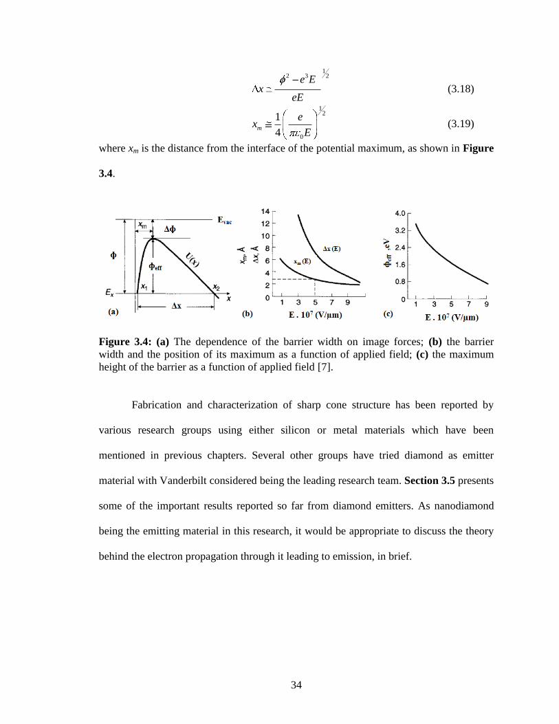
Figure 3.11 Energy band of diamond with dopants’ energy levels ..................................47
Figure 3.12 Energy band diagrams explain the (a) shallow trap and (b) deep trap energy
levels in an n-type material [154] ......................................................................................49
Figure 3.13 (a) SEM micrograph of a high density sharpened diamond tips array, inset
shows the high magnification image; (b) I-V and F-N plots (inset) for different growth
recipes; (c) a typical nanodiamond vertical transistor structure; (d) corresponding dc
characteristics .....................................................................................................................53
Figure 3.14 SEM micrographs of the nanodiamond lateral devices. (a) A 6-fingered
emitter, showing the intentionally undercut silicon layer beneath the nanodiamond; (b) a
section of a 125-fingered emitter; (c) a 2000-fingered comb array device; (d) Field
emission characteristics (I-E) of the ND lateral devices ....................................................54

xii
Figure 3.15 (a) SEM micrograph of a completely integrated nanodiamond lateral field
emission triode; (b) corresponding triode characteristics (Ia-Va-Vg) of the one-finger
nanodiamond lateral field emitter device, inset shows F–N plot; (c) monolithic diamond
lateral vacuum transistor; (d) corresponding DC transistor characteristics .......................55
Figure 3.16 (a)-(b) Field emission vacuum diode structure and symbol respectively; (c)-
(d) Field emission vacuum triode structure and symbol respectively ...............................58
Figure 4.1 Raith eLiNE electron beam lithography (EBL) tool .......................................62
Figure 4.2 Basic design of a sub-micron gap multifinger nanodiamond lateral field
emission diode ...................................................................................................................64
Figure 4.3 Basic design of a nanodiamond lateral multifinger field emission triode .......66
Figure 5.1 (a) Schematic diagram of a typical ASTeX® MPCVD system; (b) snapshot of
the CH4/H2/N2 plasma during nanodiamond deposition ....................................................68
Figure 5.2 SEM micrographs of deposited nanocrystalline diamond film grown by
CH4/H2/N2 MPECVD process technique at different conditions as shown in Table 5.1….
............................................................................................................................................70
Figure 5.3 (a) The high magnification SEM of the nanodiamond film to be used in this
research with average grain size of 5-10 nm deposited by CH4/H2/N2 microwave plasma
CVD process; (b) Corresponding cross-sectional view shows the thickness of the film…
............................................................................................................................................71
Figure 5.4 SEM of nanodiamond film coated with Al as masking material; (a) Al
thickness during the trial run; (b) Al thickness used throughout this research ..................74
Figure 5.5 Single-mask fabrication process for the micron-gap nanodiamond lateral field
emission diodes ..................................................................................................................76
Figure 5.6 SEM micrograph of four different devices (a) 125 finger diode; (b) 650 finger
diode; (c) 2000 finger diode; and (d) 9000 finger diode ...................................................78
Figure 5.7 High magnification SEM micrograph of the fabricated devices (a) 125 finger
diode; (b)-(c) comb shape configurations; and (d) higher magnification of a comb .........79
Figure 5.8 Mixed lithography fabrication approach schematic for the multifinger
nanodiamond lateral field emission triodes .......................................................................81
Figure 5.9 (a) SEM micrographs show the controlled e-beam exposure along the tip area.
(b) The substrate Si layer has been etched selectively to expose the box SiO2 in desired
places..................................................................................................................................82

xiii
Figure 5.10 a) SEM micrographs show the controlled etching has been achieved using
device Si layer of SOI wafer as hard mask. (b) The substrate Si layer has been exposed in
selective places…...............................................................................................................83
Figure 5.11 Mixed lithography fabrication approach schematic for the multifinger
submicron-gap nanodiamond lateral field emission diodes ...............................................86
Figure 5.12 (a)-(d) SEM micrographs of a 140-finger lateral nanodiamond field emission
diode with 300 nm interelectrode distance ........................................................................87
Figure 6.1 Schematic test set-up of the vacuum field emission lateral diode ...................89
Figure 6.2 Schematic test set-up for of the vacuum field emission lateral triode .............90
Figure 6.3 (a) Field emission characteristics of the nanodiamond lateral diodes in
discussion, showing the current enhancement obtained by increasing the emitter area. (b)
Corresponding Fowler-Nordheim behaviors indicates field emission ...............................93
Figure 6.4 (a) The standard symbol for a two-input OR gate and its Boolean expression;
(b) Corresponding truth table; (c) A diode OR circuit for positive diode-resistor logic,
where V(1), V(0) and V(R) corresponds to logic high, logic low and reference voltage
respectively ........................................................................................................................95
Figure 6.5 Oscilloscope images of Logic OR behavior for nanodiamond 125-finger
lateral diodes with 4 μm anode–cathode gap connected in circuit. ...................................96
Figure 6.6 Oscilloscope images of Logic OR behavior for nanodiamond 325-finger
lateral diodes with 4 μm anode–cathode gap connected in circuit ....................................96
Figure 6.7 Oscilloscope images of Logic OR behavior for nanodiamond 2000-finger
lateral diodes with 4 μm anode–cathode gap connected in circuit ....................................97
Figure 6.8 Oscilloscope images of Logic OR behavior for nanodiamond 9000-finger
lateral diodes with 4 μm anode–cathode gap connected in circuit ....................................97
Figure 6.9 Schematic representation of decrement in input logic highs with increasing
number of emission sites to maintain same output logic high ...........................................99
Figure 6.10 (a) A basic half-wave rectifier circuit; (b) Oscilloscope images verify the
half-wave rectification; (c) A linear envelope demodulator circuit; (d) Oscilloscope
images verify the envelope detection ...............................................................................101
Figure 6.11 (a) Triode emission characteristics of the nanodiamond lateral device
operating in mode-1 (handling Si as anode); (b) Corresponding F-N plots are calculated
by taking Vt into consideration .........................................................................................105

xiv
Figure 6.12 (a) Triode emission characteristics of the nanodiamond lateral device
operating in mode-2 (handling Si as gate); (b) Corresponding F-N plots are calculated by
taking Vt into consideration ..............................................................................................106
Figure 6.13 The emission behavior of the lateral triode was found to be very stable. For
example, at 45V, applied to both anode and gate, Ia was found to be 13 μA over a time
period of 10 hours’ time with 2% fluctuation ..................................................................107
Figure 6.14 (a) I-V characteristics of the fabricated 140-finger diode with 300 nm anode-
cathode distance at different temperature; (b) Stable emission current of 5, 10 and 15 µA
with little fluctuation at 8.31 V/µm, 9.86 V/µm and 11.21 V/µm respectively ..............109
Figure 6.15 Three different mechanisms dominate the electron emission. At lower field
(E < 20 V/μm), it follows F-N equation which is then followed by space-charge limited
conduction (SCLC) at moderate field (20 V/μm < E < 40 V/μm) and finally at higher
field (E > 40 V/μm) thermal-field emission (TFE) model dominates ..................... 111-112
Figure 6.16 Fitting the obtained data, upto 20 V/µm, in different mathematical models as
mentioned in Table 6.1. (a) Field Emission, best r2 value with negative slope; (b) Space-
Charge Limited Conduction, slope value > 2; (c) Thermal Field Emission, poorer r2
value; (d) Transition Region, not a straight line fit; (e) Frenkel-Poole conduction, not a
straight line fit; (f) Space-Charge Limited Conduction with Frenkel-Poole effect, worst r2
value .................................................................................................................................113
Figure 6.17 Fitting the obtained data, from 20 V/µm to 40 V/µm, in different
mathematical models as mentioned in Table 6.1. (a) Field Emission, mismatch in slope
direction; (b) Space-Charge Limited Conduction, best r2 value with slope ~2; (c) Thermal
Field Emission, poorer r2 value; (d) Transition Region, not a straight line fit; (e) Frenkel-
Poole conduction, not a straight line fit; (f) Space-Charge Limited Conduction with
Frenkel-Poole effect, mismatch in slope direction ..........................................................114
Figure 6.18 Fitting the obtained data, beyond 40 V/µm, in different mathematical models
as mentioned in Table 6.1. (a) Field Emission, mismatch in slope direction; (b) Space-
Charge Limited Conduction, slope value < 2; (c) Thermal Field Emission, best r2 value;
(d) Transition Region, not a straight line fit; (e) Frenkel-Poole conduction, mismatch in
slope direction; (f) Space-Charge Limited Conduction with Frenkel-Poole effect,
mismatch in slope direction .............................................................................................115
Figure 6.19 Energy band diagrams explain the three different emission mechanisms.
With the higher applied field the Fermi level moves up, i.e. qV<qV’<qV’’ and the voltage
drops inside the film increases, i.e. ΔV<ΔV’<ΔV’’. Also, the barrier height lowering due
to image charge at higher field is more, i.e. ΔΦ2>ΔΦ1. (a) Electron emission governed by
F-N at low field; (b) SCLC mechanism at moderate field; and (c) TFE at higher field; the
additional energy ΔE is provided by internal tip heating ......................................... 119-120

xv
Figure 6.20 Proposed microstructure for the nanodiamond vacuum lateral emitter array
three-terminal devices with 3-D gate ...............................................................................122
Figure 6.21 Few SEM images of the nanodiamond lateral emitter array vacuum three-
terminal devices with 3-D gate. (a) After pattern transfer on nanodiamond and
development; (b) Al coating to form metal lines (before ZEP520A lift-off); (c) Top view
of a defect free area; (d) High-magnification inclined view; (e)-(f) Discontinuous metal
line....................................................................................................................................125
Figure 6.22 (a) Present design of a nanodiamond lateral multifinger field emission
transistor; (b) Proposed microstructure for the nanodiamond lateral emitter array vacuum
three-terminal devices with deeper anode ........................................................................125
Figure 6.23 SEM images of the nanodiamond lateral emitter array vacuum three-terminal
devices shows that un-optimized handling Si etching resulted in cracks and bending in
the diamond film ..............................................................................................................125

xvi
LIST OF TABLES
Table Page
Table 1.1 Comparison of vacuum microelectronic & solid-state electronic
devices……………………………………………………………………… …………….3
Table 1.2 Material properties of diamond, silicon and metal for field emission
applications ..........................................................................................................................6
Table 2.1 Properties of CVD diamond and single-crystal diamond .................................11
Table 2.2 Typical surface nucleation densities of diamond after various surface
pretreatment conditions ......................................................................................................14
Table 5.1 Summery of the process parameter variation associated with respective
samples ...............................................................................................................................70
Table 6.1 The most common mechanisms of electron conduction, their expected current-
voltage relations and mathematical relations required for a straight line plot [106, 175-
176]. .................................................................................................................................112
Table 6.2 The coefficient of determination (r2) for the straight lines of best fit for
different data plots given at Table 1. (BOLD digits indicate best fit) .............................116
1
CHAPTER I
INTRODUCTION
1.1 Overview of vacuum tubes and vacuum microelectronics
The invention of solid-state transistors in 1947 [1] and the development of
integrated circuits in 1958 [2,3] had influenced scientists to believe that the time of using
large, fragile, and inefficient vacuum tubes was over. Compared to the tiny, fast and
reliable solid-state transistors, thermionic tubes required a vacuum to operate and used a
cathode heated to over 1000 C to generate the electrons which required a huge power in
performing a similar electronic task. For example, the first computer, ENIAC, had about
18,000 vacuum tubes, consumed a massive 200 kW of power and weighed over 30 tons
[4]. Consequently, solid-state transistors and ICs have replaced vacuum tubes in almost
every application of modern microelectronics and computing.
However, the rebirth of the vacuum tube in microstructure has generated renewed
interests in the exploitation of vacuum microelectronic devices (VMDs) for many new
applications such as high power and/or high frequency devices, e.g. medical X-ray, RF
for magnetic resonance imaging (MRI) machines, high voltage switching of computed
tomography (CT) scanners, electronic warfare, radar and communication systems,
industrial RF heating and welding, and radio and television broadcasting industries [5].
Unlike thermionic vacuum tubes, these VMEs devices are micro-structured vacuum
devices fabricated using sate of the art semiconductor microfabrication technology. These
devices are sometimes referred to as cold cathode field emitters. The main feature in

2
VMEs devices is the ballistic electron transport in vacuum which is more efficient than
the collision-dominated and mobility-limited transport in solid-state semiconductors. This
fundamental difference results in no dissipation of energy, a very small electron transport
time, almost independent of the ambient temperature and insensitive to radiation damage.
To generate free electrons in vacuum, the three most frequently applied
mechanisms are thermionic emission, field emission and thermionic-field emission.
Concisely, in thermionic electron emission process [6], the cathode is heated up to a very
high temperature (>1000ºC) in order to increase the internal thermal energy of electrons
so that they can overcome the work function or surface potential barrier of the material to
escape into vacuum. On the contrary, field emission is the process [7] of extraction of
electrons from a solid by applying intense electric fields across the vacuum. In this case,
electrons quantum-mechanically tunnel through the surface potential barrier into vacuum.
Lastly, thermionic-field emission process [8] involves both thermal heating and
application of electric field in the electron emission process. Details of electron field
emission theory proposed by Fowler-Nordheim which is used in this research are
discussed in Chapter III.
These “junction-free” vacuum devices also possess high-speed and long lifetime.
These characteristics are favorable for employing vacuum microelectronics in many
additional applications such as active elements in integrated circuits, field emitter arrays
for flat panel displays, large-area electron guns for high-definition television, scanning
electron microscopy and e-beam lithography [9-11]. However, the electron transport in
VMDs is limited by the crystal lattice of the emitting material, placing a bar on both the
miniaturization and the switching speed of active electronic devices. Table 1.1

3
summarizes the device properties of vacuum micro/nanoelectronic devices and solid-state
devices for promising applications [12].
Table 1.1: Comparison of vacuum microelectronic & solid-state electronic devices
Because of the above mentioned advantages, the search for the appropriate
material as electron field emitters with low operating voltage, high and stable emission
current for potential applications has been the core research of vacuum microelectronics

4
for last several decades. Recent works on field emission have been focused on the use of
electric field enhancement on sharp microtips and low work function emitter materials.
The hunt for appropriate material for VMEs devices started in early 1960s with
metal field emission diodes and triodes [13- 23]. However, they have limited potential
applications due to their high work functions which led to high threshold electric fields.
Further, the problem of impurity adsorption on metal surfaces contributed to current
instability and therefore, ultra high vacuum condition is required for stable operation.
Therefore, several approaches such as thermal annealing [19] and co-adsorption of
silicon (Si) and titanium (Ti) on tungsten (W) [24] have been proposed to improve the
stability and emission characteristics of the metal cathode. However, these approaches
increased the complexity of the fabrication process rather than significant performance
improvement. Several other materials such as GaN [25-27], BN [28], ZrN [29], GaAs
[30], and resist polymers [31] have also been reported as electron emission material.
However, electron field emitters made of these materials did not shown promising
performance for potential applications.
Next, silicon field emission devices have been studied because of well-established
silicon based microfabrication technology [32-43] which makes mass production of the
emitters possible. Diodes and triodes have been developed as the candidate for VME
devices. The silicon cathode is usually heavily doped (n+) to achieve low work function
(Φ ≈ 4.12 eV) and good ohmic contact with metal. The potential drop across the
depletion region in the n+ silicon is generally very small compared to the potential drop
across the vacuum gap because only small voltage is required for electrons to quantum-
mechanically tunnel through the thin depletion potential barrier into the conduction band

5
of n+ silicon. Thus, it is practical to assume that most of the potential drop across the
vacuum gap. The electric field at the apex allows electrons in conduction band of silicon
to quantum-mechanically tunnel through the silicon-vacuum potential barrier into the
vacuum and finally, they are accelerated by the electric field and collected at the anode.
But their field emission characteristics are relatively poor due to inadequate electrical,
thermal, mechanical, and chemical properties. For example, silicon field emitters, like
metal emitters, are very sensitive to impurity adsorption and thus require extremely high
vacuum condition for a stable operation. In addition, poor thermal conductivity and low
electric breakdown field prohibits its use in high power as well as high emission current
applications. Further, emission current has been found to degrade with time and
eventually the device has destroyed due to heat accumulation and atomic migration [44-
45]. Therefore, despite comprehensive efforts to develop efficient cathodes, only a
limited number of VME devices have moved to actual prototypes. These include
silicidation by metal adsorption [46-47], surface coating with different materials such as
TiN [48], and advanced emitter structures such as p+-n
++ junction [49], MOSFET [50],
MIS cathode [51-52], MOS cathode [53-54], porous silicon diodes [55] and hybrid
integration of field emitter arrays (FEAs) with solid-state MOSFETs or JFETs [25].
Again, as before, these techniques result in complicated fabrication processes with little
improvement in device performances and applicability in certain areas.
Recently, beside metal and Si cathodes, researchers working on VMEs have been
searching for alternate cold cathode materials, primarily allotropes of carbon; diamond,
diamond-like-carbon (DLC) and CNTs. Electron field emissions from diamond or
diamond-coated surfaces have been shown experimentally to yield large currents at low
6
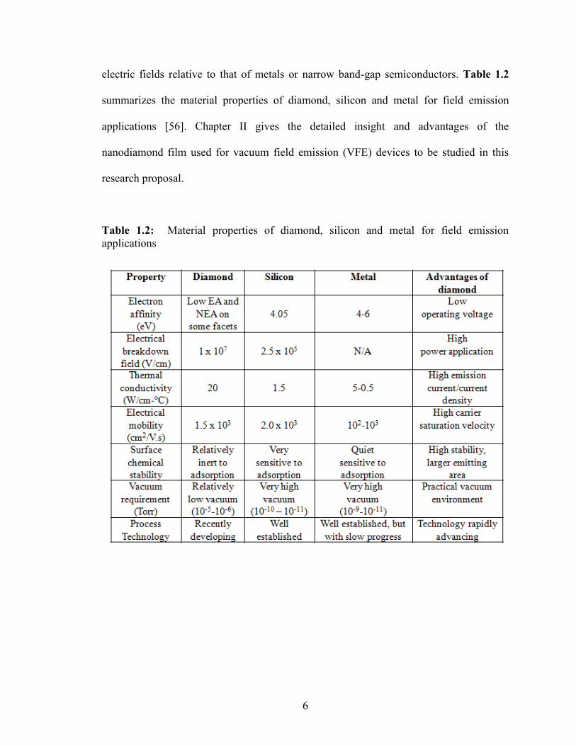
electric fields relative to that of metals or narrow band-gap semiconductors. Table 1.2
summarizes the material properties of diamond, silicon and metal for field emission
applications [56]. Chapter II gives the detailed insight and advantages of the
nanodiamond film used for vacuum field emission (VFE) devices to be studied in this
research proposal.
Table 1.2: Material properties of diamond, silicon and metal for field emission
applications
7
1.2 Motivation
This work was mainly motivated by the apparent advantages of vacuum
microelectronic devices over solid-state microelectronics and thermionic devices [57]:
Electrons travel much faster in vacuum with less energy lost and dissipation than
semiconductor devices. Because of optical and acoustic phonons scattering, the
speed of electrons in solid-state is limited by the carrier saturation velocity of the
solid (~105 m/s in silicon); whereas in vacuum, electrons’ speed is limited only by
the fundamental speed of light, ~3 x 10⁸ m/s.
Fast modulation with high electron energy is possible in VMDs devices. The
operating speed is limited only by the speed of light and device capacitance.
VMDs should hold high temperature and radiation tolerance, high reliability and
long life properties than solid-state devices which are primarily dominated by
electron scattering transport in semiconductors. This creates damages to the
crystal structure leading to spurious signals and general performance degradation.
Electron field emission can provide higher current density than thermionic
emission.
VMDs can operate at room temperature. Thus, eliminates the high operating
temperature requirement, as in vacuum tube.
VMDs can operate much faster than the traditional vacuum tubes because of their
small size.

8
1.3 Objective of this research
The scope of this research is focused on developing a reliable and consistent
process technique to fabricate submicron-gap diodes and multi-finger triode based on
nanocrystalline diamond thin films and to study their electron field emission
characteristics. The idea is to develop integrated-circuits compatible vacuum devices
operable at lower voltages or electric fields with higher emission currents for applications
of vacuum micro/nanoelectronics in harsh environment. This study may be classified as
follows:
Development of consistent process techniques for micropatterning diamond to
realize useful microstructures using dry etching techniques and multilevel mixed
lithography, viz. optical and electron beam lithography (EBL) approach.
Implementation of fabricated micro-gap nanodiamond lateral diode for vacuum
logic function realization and other applications.
Design and fabrication of micropatterned monolithic nanodiamond field emission
multifinger triodes using EBL.
Design and fabrication of micropatterned monolithic nanodiamond field emission
diodes with sub-micron gap interelectrode distance using EBL.
Electrical characterization of the fabricated nanodiamond vacuum field emitter
devices.
9
1.4 Organization of the dissertation
There are seven chapters in this report and they are organized in the following
topics:
Chapter I provides an overview of vacuum tubes and vacuum microelectronics. In
addition, the motivation, objectives and organization of this research are defined.
Chapter II is dedicated to introduce the material used in this research,
nanocrystalline diamond, and its unique properties, with particular emphasis on its
applicability to vacuum micro/nanoelectronics.
Chapter III contains a theoretical background of basic electron emission in
vacuum. It describes the basic electron conduction mechanisms through
nanodiamond leading to electron emission. This chapter also provides an
extensive survey of recent theoretical and experimental work on diamond field
emission.
Chapter IV explains the proposed research and the methodological approaches to
be used to achieve the objectives.
Chapter V describes the details of experimental, consisting of material and device
processing, with the corresponding SEM images and discussion.
Chapter VI presents the vacuum electrical characterization techniques and the
field emission performance of all devices developed, followed with analysis and
discussion of the device performance.
Chapter VII summarizes the accomplishments of the proposed research and
recommendations for future work.
10
CHAPTER II
NANOCRYSTALLINE DIAMOND
Diamond has the most extreme physical properties of any material, yet its
application in science and/or engineering has been limited due its scarcity and expense. It
is the high-pressure form of carbon with sp3-tetrahedral bonded cubic structure. Face-
centered cubic structure of the diamond crystal shown in Figure 2.1 [58], can be viewed
as two interpenetrating face-centered cubic lattices shifted along the body by (a/4, a/4,
a/4), where ‘a’ is the dimension of cubic unit cell. With the recent development of
techniques for depositing thin films of diamond on a variety of substrate materials, we
have the ability to exploit its various properties in many new and exciting applications.
As this research oriented towards the development of promising cold cathode material
using chemical vapor deposited (CVD) nanocrystalline diamond, it would be appropriate
to dedicate a chapter to explain the basic science and technology underlying of the CVD
diamond thin films and its rapid advancements in various fields including vacuum
nanoelectronics, NEMS, biomedicine, electrochemistry, optics, and beyond.
2.1 Introduction to CVD diamond
CVD processes offer an opportunity to exploit many desirable physical properties
of diamond. As Table 2.1 [59] shows, diamond is the hardest known material with lowest
coefficient of thermal expansion, is chemically inert and wear resistant, offers low
friction, has high thermal conductivity, is electrically insulating and optically transparent

11
Figure 2.1: Face-centered cubic structure of the diamond crystal [58].
Table 2.1: Properties of CVD diamond and single-crystal diamond
12
from the ultra-violet (UV) to the far infrared (IR) [60]. In most CVD methods, diamond
nucleation on non-diamond surfaces without pretreatment is usually very difficult and
slow. Most of the earlier studies on the low pressure CVD (LPCVD) diamond have
focused on examining various deposition techniques and characterizing the deposited
films which have led to a reasonable understanding of growth mechanisms and
processing parameters. Figure 2.2 shows some of the common types of LPCVD reactors
[61]. Extensive work [62-73] has been performed on the nucleation and early growth
stages to enhance the diamond nucleation to control film morphology. Thus, technical
problems associated with the nucleation of polycrystalline diamond films have been
adequately addressed. A number of nucleation enhancement methods [74-81] have been
developed to enable the control of nucleation density over several orders of magnitude. It
has been increased from <105 cm
-2 on untreated substrates to 10
11 cm
-2 on scratched or
biased substrates. The effects of surface conditions and deposition parameters on the
nucleation process have been investigated [82-85] in details to provide the guideline for
the selection of optimum surface pretreatment methods and deposition parameters.
Recently, advancements in experimental measurement method make it possible to
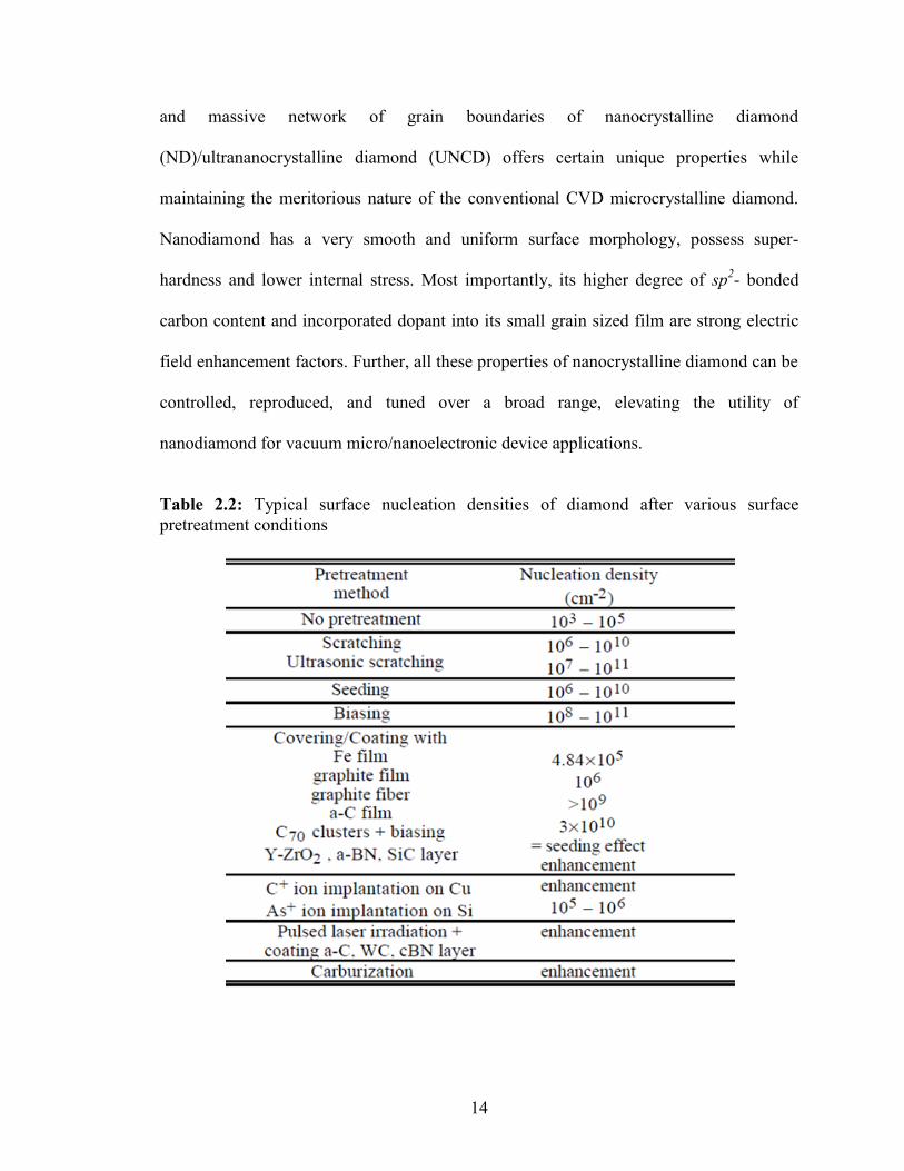
directly observe the nucleation stages. Table 2.2 gives the details of surface nucleation
densities of diamond after various surface pretreatments. The experimental investigations
have significantly contributed to understand the nucleation mechanisms in diamond CVD
process which may allow diamond to realize its potential as an electronic material in the
near future.
But the conventional CVD microcrystalline diamond is not used widely for
applications in micro/nanoelectronic devices, optical devices, nanoelectromechanical

13
Figure 2.2: Example of common types of LPCVD reactors [61]. (a) Hot filament; (b)
‘NIRIM-type’ microwave plasma reactor; (c) ‘ASTEX-type’ microwave plasma reactor
and (d) DC arc jet.
systems (NEMS) and thermal management devices. It is very important to modify this
material to feed-in to suitable application. To achieve this, the processing challenges and
the difficulties encountered in applying diamond in thin film and device forms can be
minimized by the development ofnanocrystalline diamond or “nanodiamond” which
possesses a grain size in the nanometer scale between 1 nm and 100 nm. Small grain size
14
and massive network of grain boundaries of nanocrystalline diamond
(ND)/ultrananocrystalline diamond (UNCD) offers certain unique properties while
maintaining the meritorious nature of the conventional CVD microcrystalline diamond.
Nanodiamond has a very smooth and uniform surface morphology, possess super-
hardness and lower internal stress. Most importantly, its higher degree of sp2- bonded
carbon content and incorporated dopant into its small grain sized film are strong electric
field enhancement factors. Further, all these properties of nanocrystalline diamond can be
controlled, reproduced, and tuned over a broad range, elevating the utility of
nanodiamond for vacuum micro/nanoelectronic device applications.
Table 2.2: Typical surface nucleation densities of diamond after various surface
pretreatment conditions

15
2.2 Morphology of nanocrystalline diamond
The grain size of a nanocrystalline diamond film can be typically controlled to be
as small as 2 nm. Figure 2.3 shows the typical cauliflower-like morphology of
nanocrystalline diamond with grain size of 15-20 nm [86]. The morphology change in the
diamond film brings with a large increase in the utility of the material. While considering
field emission, the nanometer range grain size results in formation of emitter tips with
ultra-small radius of curvature, leading to a high geometrical field enhancement factor.
Further, the increased grain boundary network can act as conduction channels, increasing
the electrical conductivity and thereby allowing better electron transport through the film.
Nanocrystalline diamond films overcome most of the drawbacks of traditional
microcrystalline diamond films as they are smooth, dense, pinhole free, phase-pure, and
can form conformal coating on a wide variety of materials. The nanocrystalline diamond
deposition technique and the effect of controlling the plasma chemistry on the
morphology of the diamond film have been explored by our research group in past [86-
87]. The SEM and atomic force microscopy (AFM) images in Figure 2.3 [86] confirm
that nanodiamond films have a smoother surface morphology and wider latitude for
materials integration than the microcrystalline microwave plasma-enhanced CVD
(MPCVD) diamond films.
The surface roughness (100-400 nm) of the CVD microdiamond film is
considered to be high for many applications. In order to overcome the problem of surface
roughness of diamond films either post-polishing should be adopted or naturally smooth
films should be grown without compromising their hardness and other useful properties.
However, post-polishing is expensive and time consuming. Nanocrystalline diamond has

16
a very smooth and uniform surface morphology with a typical RMS surface roughness of
8-20 nm, independent of the film thickness. The smoothness of the thin film is directly
related to its mechanical properties like coefficient of friction relevant to MEMS, and is
also a very critical factor in several cases including micropatterning of diamond films to
realize useful structures, and integration of different materials with diamond.
Figure 2.3: SEM and AFM images of nanocrystalline and microcrystalline MPCVD
diamond films [86].
2.3 sp2/sp
3 composition of nanocrystalline diamond
Nanodiamond is highly sp3-bonded in nature. Due to the decrease in the grain size
and increase in the volume density of grain boundaries, nanodiamond films encompass
increased sp2-bonded non-diamond carbon content, preferentially in the grain boundaries
[86]. It is known that the intensity and broadening of Raman peaks are directly correlated

17
to the crystal size of films. A broad sp3-diamond
peak (1332 cm
-1) and higher sp
2-carbon
shoulder (1560-1580 cm-1
) are typical characteristics of the Raman spectrum obtained
from a nanodiamond film, as shown in Figure 2.4 (a), in comparison with that of a
conventional microdiamond film (grain size: 1 µm-3 µm), featuring a sharp sp3-diamond
peak and a very small sp2-carbon signature, Figure 2.4 (b). The visible Raman
spectroscopy is mainly suitable to monitor the sp2-carbon behavior and follow the
evolution of sp2-carbon phase. It often gives rise to an intense background
photoluminescence that can mask the Raman line in nanodiamond, even in films with low
amounts of sp2–bonded carbon. Also, Raman scattering in visible range is about 50 times
more sensitive to the sp2-bonded carbon than the sp
3-bonded carbon [88-91].
UV–Raman spectroscopy using higher photons energy (shorter wavelength) can
characterize the nature of sp3-bond in the films more clearly [92]. Figure 2.5 (a) - (b)
show the typical visible and UV Raman spectra of nanocrystalline diamond films
respectively. The peak at 1332 cm− 1
, characteristic to sp3-bonding, which is not easily
resolvable in visible Raman spectroscopy, is clearly observed in Figure 2.5 (b). Also, it
can be seen that the ratio of the diamond (1332 cm-1
) to the nondiamond (1560 cm-1
)
band intensities, is large for the film deposited without any added N2 and decreases for
the films deposited with the gas. One of the theories suggests that, increasing the N2 in
the source gas mixture causes an increase in the relative number of grain boundaries in
the film, and it is at these grain boundaries that the sp2-bonded carbon atoms exist [93].
The presence of sp2-carbon as a strong field enhancement factor for electron emission has
been discussed in Chapter III.

18
Figure 2.4: (a) Visible Raman spectrum of a nanocrystalline diamond film with 3-5 nm
grain size; (b) Typical Raman spectrum of a microcrystalline diamond film [89-91].

19
Figure 2.5: (a) Visible Raman spectra of nanocrystalline diamond films deposited from
0, 2, 4, and 10% N2 in CH4/Ar/N2 source gas mixture; (b) UV Raman spectra of
nanocrystalline diamond films deposited from 1, 5 and 10% N2 in CH4/Ar/N2 source gas
mixture [92-93].
2.4 Nitrogen as an n-type dopant in nanocrystalline diamond
The success in fabricating diamond-based electronic devices has been limited
mainly due to the difficulty in achieving the effective n-type diamond. The problem lies
in the difficulty of finding a way to dope diamond so that its conductivity and carrier
mobility are sufficiently high to make diamond-based devices work at room temperature.
Nitrogen is among a few suitable dopants for nanocrystalline diamond. But, traditional
doping with nitrogen does not work, since nitrogen atoms at substitutional sites introduce
a deep donor level 1.7 eV below the conduction band, and thus is not thermally activated
at room temperature [94-95]. Unlike nitrogen doped single crystal diamond or
microcrystalline films, nanodiamond, due to its small grain size and thereby a high
density of grain boundaries, allows for easier incorporation of nitrogen impurities [96-
100]. Secondary ion mass spectroscopy (SIMS) data has shown that the content of
nitrogen in the UNCD film saturates at 2x10²⁰
atoms/cm3 (~ 0.2 % total nitrogen content
in the film), Figure 2.6 (a)-(b), when the nitrogen concentration in the plasma is 5 %

20
[96]. The conductivity at room temperature increases dramatically with nitrogen
concentration, from 0.016 (1 % N2) to 143 Ω-1
cm-1
(20 % N2), Figure 2.6 (c) [96].
Further, the nitrogen incorporation has been confirmed to be consistent through the depth
of the film, shown by the profiles of the carbon and nitrogen concentrations as a function
of depth for a nanocrystalline diamond film deposited from 1% CH4/5% N2/95% Ar, [93]
Figure 2.6 (d).
Researchers, including our group have reported successful nitrogen incorporation
and high electrical conductivity in nanocrystalline diamond. The high electrical
conductivity of nanodiamond obtained from CH4/H2/N2 plasma is attributed to the In-situ
addition of nitrogen gas to the growth chemistry in the MPECVD process. Energy
dispersive spectrometry X-ray microanalysis revealed the incorporation of nitrogen in the
nanodiamond film, Figure 2.7 (a) which displays a real time histogram of X-ray count
per channel versus energy expressed in keV [86]. The nanodiamond film profile exhibits
the characteristic carbon and nitrogen elemental peaks at X-ray energies of 0.277 and
0.392 keV, respectively. Further, RBS experiments conducted [86] on the CH4/H2/N2-
plasma derived nanodiamond film also indicated the incorporation of nitrogen. The semi-
log RBS plot, Figure 2.7 (b), displays a distinct nitrogen edge, thus confirming the
presence of nitrogen in the nanodiamond. An idea of the nitrogen distribution profile can
be obtained using the graph. While the edge, typically occurring at 565 keV according to
the RBS calibration, shows that nitrogen is present at the surface of the film, the step-like
profile is indicative of nitrogen also distributed in the nanodiamond bulk. Quantitatively,
the nitrogen concentration was found to be ~ 4.5×10²¹
cm−3
in the near-surface region (~
50 Å) of the nanodiamond film. The actual percentage composition was ~ 1.45 %. RBS,

21
being a surface-sensitive technique, could be used to accurately verify the nitrogen
concentration in the near-surface region. The electrical conductivity of nanodiamond can
be enhanced by increasing the percentage of nitrogen included in the growth plasma.
Another effective technique to achieve nitrogen-doping in nanocrystalline diamond is to
increase the microwave power and pressure at a particular nitrogen gas flow rate.
Figure 2.6: (a) High-resolution SIMS spectra of the UNCD film revealing the
incorporation of nitrogen with a CN- secondary ion peak with a mass of 26.0030 amu; (b)
Total nitrogen content and room-temperature conductivity as a function of nitrogen in the
plasma; (c) Arrhenius plot of conductivity data obtained in the temperature range 300–4.2
K for UNCD films synthesized using different nitrogen concentrations in the plasma; (d)
Depth profiles for the atomic carbon and nitrogen concentrations in a 1 µm-thick NCD
film [93,96].

22
Figure 2.7: (a) EDS x-ray microanalysis composition profile (X-ray count Vs Energy) of
the nanodiamond film deposited by CH4/H2/N2 MPECVD, indicating the incorporation of
nitrogen impurity in the diamond film; (b) Semi-log RBS plot (backscattered ion count
vs. energy) obtained from the CH4/H2/N2-nanodiamond possessing a distinct nitrogen
edge in its composition profile [86].

23
2.5 Effect of growth temperature
In most CVD processes, substrate temperature is set to above 700 °C to obtain
high quality crystalline diamond films at reasonably high deposition rates which have
greatly limited the applications of diamond films in microelectronic devices. Therefore,
reducing the substrate temperature during deposition without sacrificing the quality of
diamond films and deposition rates comparable to those characteristic of high-
temperature growth, is of great scientific and practical significance. Researchers [101-
102] have shown successful dense and continuous ND/UNCD film synthesis at
temperatures as low as 400 °C using optimized ultrasonic seeding process. The
nanocrystalline diamond growth process plasma chemistry exhibits much less
temperature dependence than the conventional microcrystalline diamond deposition
process. The temperature dependence of the UNCD deposition is reflected in the
microstructural development shown in the SEM micrographs, Figure 2.8 (a)-(b). The
UV-Raman spectra of the UNCD films prepared at different temperatures are shown in
Figure 2.8 (c). There are three prominent peaks in this spectrum, with a clear diamond
peak at 1332 cm−1 that increases in intensity as the deposition temperature decreases.
The peak labeled N2 is due to nitrogen gas present along the optical path of the
spectrometer. This reported development signals a suitable platform material for
application to diamond-based stand alone microelectronic and/or integrated
microelectronic/microelectromechanical systems (MEMS) devices. Deposition at low
temperatures can enhance the feasibility of integrating diamond with other materials, and
can pitchfork its application in integrated circuits and other applications, Figure 2.8 (d).

24
Figure 2.8: (a)-(b) SEM images of the surface morphology and corresponding cross-
section of UNCD films deposited at 800 C and 400 C; (c) UV-Raman spectra of UNCD
films deposited at various temperature; (d) Low temperature UNCD as hermetic coating
for BioMEMS, showing the materials integration feasibility offered by the material
[86,101-102].
So far, this chapter elucidates how the unique properties of nanocrystalline
diamond can be favorable for electron field emission. Nitrogen-incorporation to
nanocrystalline diamond makes it electronically active, while retaining the thermal and
mechanical stabilization properties of the diamond material, making it a highly potential
and reliable candidate for electron emitter. The possible electron conduction mechanisms
through bulk diamond resulting in emission current have been discussed in Chapter III.
Later, Chapter V describes the process techniques and exact parameters developed for
growing nanodiamond film used in this research.
25
CHAPTER III
ELECTRON EMISSION and VFED OPERATING PRINCIPLES
This chapter reviews the theoretical aspects of electron emission in detail and the
present understanding of the possible electron emission mechanisms from CVD diamond.
Following that, some of the important results reported so far from diamond emitters are
presented. Last but not least, the basic operating principles of VFE devices, such as diode
and triode, are presented.
3.1 Basics of electron emission into vacuum
Electron emission is the process of emitting electrons from a solid surface into
vacuum under external influences, viz. electric field or heat or both. The three most
common processes of electron emission are thermionic emission, thermionic-field
emission, and field emission. In each of these processes, energies in form of either heat or
electric field or both are exerted on the solid to extract electron. The mechanisms for
these processes can be explained by considering the energy band diagram [87] of a metal-
vacuum system as shown in Figure 3.1.
For thermionic emission, electrons emit into vacuum at very high temperature of
1500-2500 °C depending on the metal work function. At 0 K, all the electrons in solid
have energy below the Fermi level (EF). With the increase in temperature, some electrons
gain kinetic energy and thus, have total energy above Fermi level. At sufficient high

26
temperature, some electrons gain total energy higher than vacuum level (Evac), (T) e- in
Figure 3.1, and readily emit into vacuum with no applied potential.
At moderate temperature, some electrons, (T-F) e- in Figure 3.1, have total
energy above EF but below vacuum level and thus, are not readily to emit into vacuum. In
order for these electrons to emit into vacuum, a moderate electric field must be applied to
thin down the potential barrier as illustrated in Figure 3.1. This thermal-field activated
emission process, via quantum-mechanical tunneling, is called thermionic-field emission.
Depending on the metal work function, thermionic-field emission from metal can be
observed at temperature range of 700-1500 °C.
Figure 3.1: Mechanisms for thermionic (T), thermionic-field (T-F), and field emission
(F) [87].
Whereas, electron field emission is a unique quantum-mechanical effect of
electrons, (F) e- in Figure 3.1, tunneling from a condensed matter (solid or liquid) into
vacuum. At low temperature, most of electrons have total energy below EF. Thus, a
strong external electric field must be applied to extract the electrons. Since, electric field
is the main energy source that induces electron emission; this phenomenon is called field

27
emission. The efficiency of this process is tens of millions of times higher than in other
known emission processes. The extremely high current density and no energy
consumption by the emission process afford exceptionally wide possibilities for practical
application of this effect. Electron emission can also occurs by other methods such as
light excitation (photoelectric electron emission), external electron energy (secondary
electron emission), and internal polarization switching (ferroelectric electron emission).
These interesting electron emission phenomena are beyond the scope of this research.
However, the basic theoretical aspects of electron field emission as the main topic of this
research are further discussed in the two following sections.
3.2 Fowler-Nordheim (F-N) theory of field emission
The original field emission (FE) theory for cold cathodes with flat surface was
first developed by Fowler and Nordheim in 1928 [103]. If an electric field is applied to
the surface of a solid, the rectangular surface potential step change into a triangular shape
which is shown in Figure 3.2. If the width of the surface potential barrier approaches ~2
nm, which is the tunneling distance for low energy electrons, the confined electrons will
quantum-mechanically tunnel from the highest occupied states in the solid into vacuum
and an emission current will be detected at the positively biased anode [7,57].
According to Fowler-Nordheim (F-N) theory, the dependence of the emission
current density, J (A/cm2), on the work function of the emitting surface, Φ (eV) and the
local electric field just above the emitter surface, E = V/d (V/cm), is exponential. The F-
N equation can be written as [103-105]:
2 3/2
1 2expI E
J k kA E
(3.1)

28
where I (A) is the emission current, A (cm2) is the emission area, and k1 and k2 are
universal constants given by:
k1 = e3 / 8 h = 1.54 x 10
-6 AeVV
-2 (3.2)
k2 = 4(2me)1/2
/ 3eħ = 6.83 x 10⁷ eV
-3/2Vcm
-1 (3.3)
where e is the elementary positive charge, me is the electron mass, h is the Planck’s
constant, and ħ = h/2 .
Figure 3.2: The field emission model for a metallic emitter proposed by Fowler and
Nordheim. Diagram shows the potential barrier and the triangular surface potential under
an applied electric field E.
The Eq. 3.1 was derived for a metal cathode with the following physical assumptions [7]:
I. The metal cathode has a free-electron band structure,
II. The electrons obey Fermi-Dirac statistics,
III. It is at 0 ºK,

29
IV. The cathode has a smooth flat surface,
V. The cathode has a work function which is uniform across the emitting surface
and independent of electric field.
VI. The electric field outside the metal surface is uniform, and
VII. The effect of image field between the emitted electrons and the surface is
neglected in a first approximation.
To include the image field effect, in 1956, Murphy and Good [106] presented a
full mathematical analysis of the standard physical assumptions in F-N theory. The result
is the inclusion of two electric field dependent elliptical functions v(y) and t2(y) in Eq.
(3.1), where y is the image charge lowering contribution to Φ given by,
2/1
3
Fky
(3.4)
where,
k3 = (e3/4 o)
1/2 = 3.79 x 10
-4 eVV
-1/2cm
1/2 (3.5)
and ε0 is the permittivity of vacuum (8.85x10⁻¹⁴
Fcm-1
).
Further, let us consider the sharp cone structure, as shown in Figure 3.3 [107]
which results in non-uniform electric field as illustrated in Figure 3.2. The electric field
is highest at the tip apex and rapidly decreases outward to the anode. Thus, the F-N
equation, Eq. (3.1), which is derived for planar cathode cannot be precisely applied. The
precise calculation of potential distribution, electric field, and emission current for a
sharp microstructure involves numerical calculation of 3-dimensional Poisson equation
and Schrodinger equation for electron emission [108-110]. However, the emission current
for a sharp microstructure can be obtained with a simple modification of Fowler-

30
Nordheim equation for a planar metal cathode by replacing the parallel electric field (E)
in Eq. (3.1), with electric field at the apex of the sharp microstructure (F) that is
F E (3.6)
where, β is defined as the geometrical field enhancement factor.
So taking all into consideration, the revised F-N equation can then be expressed as [7]:
2 3/2
1 22
( ) ( )exp
( )
I E v yJ k k
A t y E
(3.7)
Figure 3.3: Series of SEM images of a 25 nm diameter Si tip emitter coated with a
UNCD film with incremental coating thickness. The tip on the left is uncoated and
successive images represent coatings ranging from 100 nm to 2.4 µm in thickness [107].
This simple approximation implies that the emission current for a sharp
microstructure, generally referred as the “Spindt cathode”, is equivalent to the emission
current of a planar cathode of the same vacuum gap but the effective electric field is
increased by the factor of β. This approximation agrees very well with experimental
results because the electric field of a sharp tip is strongest at the apex and reduced rapidly
for the region away from the apex and hence, it can be assumed that most of emission

31
current arises from electron tunneling within the vicinity of this highest electric field
region. Thus for FE, electrons with energies below the EF predominates and tunneling
through field dependent barrier is mainly responsible for variation in emission current at
low temperature. FE can be verified by a straight line with a negative slope by plotting
the one over electric field (1/E) as abscissa (x-axis) and the Ln(J/E2) as the ordinate (y-
axis).
3.3 Theory of Thermionic-Field emission
As the field emission equation is independent of temperature term, a diversion of
the experimental data from the F-N straight line has been observed at moderate or high
temperature. In 1956 [106], Murphy and Good presented an elaborated calculation
considering the thermal effect on field emission. In absence if any external heating,
Dolan and Dyke [111] used an internal tip heating model to calculate the steady state
temperature rise at the tip which is given by:
2 2T aJ r (3.8)
where a depends on the emitter cone angle and r is the tip radius. In brief, as proposed by
them in 1953, there are two main sources of energy which cause heating of the tip during
field emission at higher field. The first is Nottingham heating, which produces a power
density input W1 (W/cm2) at the tip surface,
1 . FW J E (3.9)
where ΔEF is the difference between EF and the average electron energy (EFavg), i.e. ΔEF
= EF – EFavg. This heating occurs at or just inside the emitter tip surface and is
proportional to the emission current density (J). As J increases, Nottingham heating

32
increases which increases the tip temperature. This results an increase in average energy
of the emitted electrons and become equal to the Fermi energy at the inversion
temperature (Ti). As temperature increases further, Nottingham cooling takes place.
Hence it tends to stabilize the tip temperature at a value near the inversion temperature.
The second energy input to the tip is resistive heating, which produces a power density
W2 (W/cm2) inside the tip,
2
2 .W J (3.10)
where ρ is the resistivity of the emitter. Thus W2 is proportional to J2 and increases as ρ
and J increases with the tip temperature increment. Hence an unstable emission could be
possible at higher current density and temperature.
The theoretical treatment of thermionic emission leads to Richardson’s equation
modified by the Schottky dependence on the square root of the applied field [112]. The
origin of Schotty barrier lowering comes from the image potential that an electron
experience near the conducting surface. The force (F’) between an electron at x into the
vacuum from the surface and its image is given by [113]:
2
2
0
'16
eF eE
x (3.11)
The potential energy is found by integrating the force from x>0 to α, resulting:
2
0 0
1( )
16 16image
x x
e eV x Edx dx
x x (3.12)
Now, under the applied electric field E:
( ) 'fieldV x F x eEx (3.13)
Thus the sum of the potential U(x) is given by:

33
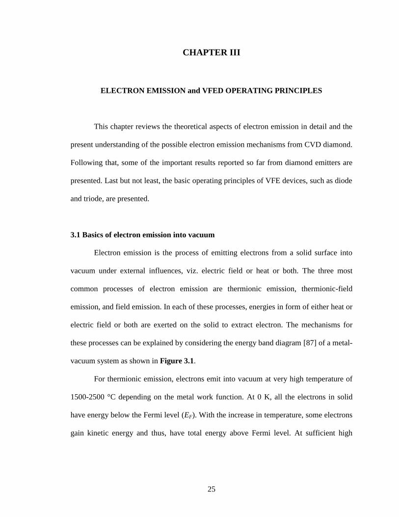
0
( )16
eU x eEx
x (3.14)
The maximum is obtained by differentiating the potential and setting equal to zero, i.e.
0
016
d eeEx
dx x (3.15)
which gives,
12
max
016
EV e (3.16)
Therefore, under applied field the surface potential barrier (Φeff) is effectively reduced to
Φ - Vmax, as shown in Figure 3.4 (a). The emission current associated with this Schottky
Barrier Lowering (SBL), namely Thermal-Field Emission (TFE), is given by [106]:
24
exp
i
i
eEe
J ATkT
(3.17)
where A is effective Richardson’s constant, εi is the material permittivity, k is the
Boltzmann constant and T is the temperature in Kelvin. TFE can be verified by a straight
line with a positive slope by plotting the square root of the electric field (E½) as abscissa
(x-axis) and the Ln(J/T2) as the ordinate (y-axis).
Under higher electric field, the dimensions of the potential barrier at the solid-
vacuum interface become on the same order as interatomic distances and the radii of
close-range interactions [7]. The width of the image force barrier, Δx = | Δx1 – Δx2|,
where x1 and x2 are the classical turning points as shown in Figure 3.4 (a), has been
calculated [7] by assuming the kinetic energy of the electrons in the direction of emission
is zero at the turning points, i.e.
34
12 3 2e E
xeE
(3.18)
12
0
1
4m
ex
E (3.19)
where xm is the distance from the interface of the potential maximum, as shown in Figure
3.4.
Figure 3.4: (a) The dependence of the barrier width on image forces; (b) the barrier
width and the position of its maximum as a function of applied field; (c) the maximum
height of the barrier as a function of applied field [7].
Fabrication and characterization of sharp cone structure has been reported by
various research groups using either silicon or metal materials which have been
mentioned in previous chapters. Several other groups have tried diamond as emitter
material with Vanderbilt considered being the leading research team. Section 3.5 presents
some of the important results reported so far from diamond emitters. As nanodiamond
being the emitting material in this research, it would be appropriate to discuss the theory
behind the electron propagation through it leading to emission, in brief.

35
3.4 Electron emission from nanodiamond
Diamond is one of the main high-pressure crystalline allotropes of carbon with
sp3-tetrahedral bonded cubic structure, as shown in Figure 3.5 [114]. When its surfaces
are terminated with hydrogen atoms, the electron affinity, which is a measure of the
energy barrier that electrons must overcome to escape into vacuum, can become negative.
Thus, the presence of low/negative electron affinity (NEA) on hydrogen-terminated
diamond surfaces, coupled with practical chemical vapor deposition (CVD) of diamond
on a variety of substrates, has attracted attention of diamond’s promise as a high
performance cold cathode material. Experimentally, diamond has been observed to emit
electrons at relatively low electric fields and generate useful current densities [87].
3.4.1 Energy band diagram of nanodiamond
Electron field emission from diamond has been experimentally observed to yield
high emission current at low applied electric field. However, the mechanisms responsible
for low field emission from diamond are not clearly understood. Diamond surfaces have
remarkable energy band diagrams, which are different from most of other
semiconductors. A complete knowledge on energy band diagram of diamond surfaces is
key information to understand electron field emission from diamond.
Diamond is an indirect wide band-gap material with Eg =5.45 eV. So far, three
distinct types of diamond surfaces have been widely studied [115-123]. Figure 3.6 (a)
illustrates hydrogen-free diamond surfaces with small positive electron affinity. Partially
hydrogenated (111) and (100) diamond surfaces have effective negative electron affinity
(NEA), as illustrated in Figure 3.6 (b). This reduction in electron affinity, together with a

36
short characteristic band bending at the surface results in the effective negative electron
affinity surface. Furthermore, diamond surface coated with a thin layer of metal such as
Zirconium (Zr), Cobalt (Co), and Ni [124-125] also exhibit effective negative electron
affinity property as illustrated in Figure 3.6 (c).
Figure 3.5 Eight allotropes of carbon (a) Diamond; (b) Graphite; (c) Lonsdaleite; d) C60
(Buckministerfullerence); (e) C540; (f) C70; (g) Amorphous Carbon, and (h) Single-
walled carbon nanotube [114].

37
Further, it is believed that a true NEA surface also exists on the Cesium (Cs) or
Cesium oxide (Cs2O) coated diamond (100) surface [126]. The occurrence of the true
NEA has not been found for conventional semiconductor materials. Assuming a diamond
surface with small positive electron affinity, a complete energy band diagram for electron
emission from that surface may be drawn as shown in Figure 3.7 [87]. For electron
emission to occur, electrons must quantum- mechanically tunnel through the potential
barrier at metal-diamond interface into diamond. Then the electrons will drift through the
bulk diamond to reach a small potential barrier at diamond-vacuum interface and finally
tunnel into vacuum under an electric field. Small or even negative electron affinity of
diamond is believed by many to be responsible for observing low field emission because
it would allow electrons from the conduction band to emit into vacuum easily with low
applied electric field. However, electron in conduction band of diamond is limited due to
its wide band gap. Thus, electron must be injected from metal into conduction band of
diamond in order for emission to occur. This requires a high electric field since the
potential barrier at metal-diamond interface would be as high as work function of silicon
or metals. Thus, the basic energy band diagram as described is inadequate for the
explanation of the observed low field emission from diamond.
In order to explain the field emission mechanism from diamond, a better
understanding of carrier transport through diamond-metal interface and the bulk diamond
film is needed. A more complete energy band structure, which includes the effect of grain
boundary and defects of polycrystalline diamond, is also required to be studied. So far,
several field emission mechanisms, carrier transport through the bulk and field emission
enhancement models for various types of diamond emitters have been proposed. The

38
following section summarizes some of the important proposed theories and models. The
low/negative electron affinity property of diamond surfaces may be important and can
make diamond an efficient emitter but it is not adequate to explain its good field emission
behavior. For field emission to occur, and sustain, there must be a continuous supply of
electrons into the bulk diamond and a sustainable electron transport mechanism through it
to reach the emitting surface. Moreover, the energy levels of these electrons relative to
the vacuum level are critical in determining the threshold field required for emission.
Figure 3.6: Energy band diagrams of diamond. (a) Positive electron affinity; (b)
Effective negative electron affinity; (c) True negative electron affinity [87].

39
Figure 3.7: (a) Diamond cathode structure; (b) Energy band diagram at thermal
equilibrium; (c) Energy band diagram under forward bias [87].

40
3.4.2 Emission mechanisms
Simple field enhancement model
Among the various models, the simplest argument cites the classic field emission
theory by considering local field enhancements on sharp morphological features
protruding from the diamond surface. The electric field at a given applied potential is
enhanced by these sharp microstructures [127] and thereby more electron tunnel into
vacuum. Field emission from diamond-microtips exhibit significant enhancement in both
total emission current and stability compared to planar diamond emitter. The geometrical
field enhancement factor β depends only on the shape of the microstructure. The figures
of merit (f) for various shapes are estimated [12] and shown in Figure 3.8. It can be
concluded that the rounded whisker shape is the closest to the “ideal” field emitter. While
on the contrary, a wide-angle pyramidal shape is very poor as a field emitter even though
it has excellent thermal and mechanical stability. Further, the electric field distribution at
the surface of a rounded whisker, Figure 3.8(a), can be evaluated in closed form as a
function of polar angle θ using elementary electrostatic theory as [12]:
3cosV hEd r
(3.20)
3coshr
(3.21)
where h is the height of the sphere from the base and r is the radius of the tip. For h>>r, E
≈ (h/r)(V/d) and β ≈ h/r. Ideally, the field at the apex of a floating sphere is given by E =
(h/r)(V/d). However, to apply the simple field enhancement model, the microstructure
must have certain geometry with a smooth surface which is not practical.

41
Figure 3.8: Various shapes of field emitters and their figure of merit; (a) Rounded
whisker; (b) Sharpened pyramid; (c) Hemi-spheroidal; (d) Pyramid [12].
Two step field enhancement (TSFE) model
This model is the modified version of the simple field enhancement model to
account for the complicated morphology of diamond surface. The emitting surface is
considered to be rough and consists of a number of small protrusions act as tiny tips. The
emitting tip with height h1 and sharpness of radius r1 is assumed to consist of a number of
tiny tips with height h2 and sharpness of radius r2 as shown in Figure 3.9 [128]. The
electric field on the blunt tip is equal to
11
1
h VEr d
(3.22)
and the field enhancement at the end of protrusions is equal to
2 1 22 1
2 1 2
h h h VE Er rr d
(3.23)
Based on the TSFE model, the emission current were calculated using the F-N analysis
from diamond coated silicon field emitters and found to be in good agreement with
experimental data. This model has also been well applied to explain the increase in the

42
geometrical field enhancement of sharpened pyramidal diamond microtips [86-87]. In
this case, the sharpened diamond microtip was modeled as a large conical tip with tip
height of h1 and tip radius curvature of r1, superimposed with a sharp tiny conical tip with
tip height of h2 and tip radius curvature of r2, as shown in Figure 3.9 (c). The electric
field at the sharpened tip apex arises from a two-cascaded tip structure. In the first step,
the electric field at the apex of large conical tip is enhanced by the factor of h1/r1 from the
planar base, while in the second step; the electric field at the apex of the sharp tiny
conical tip is enhanced by the factor of h2/r2 from the apex of large conical tip. Thus, the
total geometrical field enhancement factor could be written as the product of the two field
enhancement factors of the cascaded tip structure:
2
2
1
1
r
h
r
hg
(3.24)
Figure 3.9: Geometry of emitters; (a) The simple field enhancement approach; (b)-(c)
Illustration of the TSFE approach [128].

43
Estimation of the geometrical field enhancement using this model was found to be in
good agreement with the result obtained from F-N analysis. However, this model does
not address the source of electrons in the wide-bandgap and effective electron transport to
the surface of diamond.
Lowering of the surface work function model
In the lowering of the surface work function model, it is assumed that the sharp
microtip and the complicated surface morphology result in significant reduction of the
surface work function. A significant enhancement in field emission after diamond coating
on silicon tip was observed which could also be attributed to the lowering of the surface
work function by diamond [128]. Although it is unclear how diamond could have
sufficient amount of electrons in or near the conduction band to produce large emission
currents. In addition, it has been found that the diamond surface work function can be
lower by coating with a low work function material such as Cs [126]. It has been found
that the diamond surface treated with O2 plasma and Cs deposition substantially enhances
the electron emission for Li-doped and N-doped diamond [129]. It has been suggested
that oxygen-terminated diamond surface reacts with Cs to form an oxygen-stable
diamond-O-Cs surface that lowers the surface work function of diamond. However, the
lowering of work function by Cs treatment for field emission enhancement is not a
practical technique because Cs is an expensive and reactive element.
Further, hydrogen treatment on diamond surfaces was found to improve field
emission characteristic significantly [120-121]. The lowering of work function of
diamond surfaces by hydrogen termination was believed to be the most probable
explanation for the observed field emission enhancement. The termination of hydrogen

44
on diamond surface is known to form a positive surface dipole that could produce band
bending and result in lowering of electron affinity and work function of diamond
surfaces. On the other hand, oxygen treatment was found to degrade field emission
characteristic of diamond surface [125,130]. The degraded emission property was
believed to cause by the increasing of work function of diamond. The termination of
oxygen on diamond surface is known to form a negative surface dipole to produce band
bending which results in increasing of electron affinity and work function of diamond
surfaces.
Defect/impurity theory
The defect/impurity theory suggests that structural defects and impurities can
form energy states within the band gap of diamond [131-132]. When the defect density is
sufficiently high, the electronic states of various defects can interact and form additional
energy bands. If these bands are wide enough or closely placed, the electron hopping
mechanism within the bands, similar to the Poole-Frenkel conduction mechanism or the
Hill type conduction [133-135] could easily provide a steady flow of electrons to the
surface and sustain a stable electron emission. The electrons can either be excited into the
conduction band or unoccupied surfaces states from these defect/impurity bands to emit,
or tunnel directly from the defect/impurity bands into vacuum. These defects/impurities
essentially raise the Fermi level by acting as donors of electrons and thus reduce the
tunneling barrier. This theory is supported by overwhelming experimental data indicating
that defective or lower quality diamonds have better emission properties. It also appears
to explain why emission characteristics are enhanced in many “doped” diamonds, not

45
necessarily because of the electrical doping effect, but rather by the creation of defects
during the doping process.
Presence sp2-carbon content in the diamond film
This model is based on the observation that active emission sites correspond to
discrete location of defects or graphite inclusions on the diamond surface [136-139]. To
sustain a continuous flow of emitting electrons, it has been assumed to be supplied to the
emitting surface through conduction channels formed in diamond via an electroforming
process at high electric fields [87]. Also, grain boundaries in diamond films [108] and
hydrogenated diamond surfaces [109,140] have been suggested to function as conduction
channels.
Wisitsorat-at [87] proposed that isolated conducting sp2 nano-particles in the
diamond film form a series of cascaded MIM (metal-insulator-metal) microstructures.
Such a particle could therefore enhance the electric field distribution locally across the
junction where it forms a contact with the electrode surface, which enhances the electric
field inside the diamond film, thereby increasing the field enhancement factor. The image
effect at the diamond-sp2
interface causes band bending in the conduction band of
diamond as illustrated in Figure 3.10. The enhanced electric field decreases the width of
tunneling distance, W, at the metal-diamond interface significantly, and thereby increases
the electron tunneling probability from metal into the conduction band of diamond. The
electrons in the conduction band of diamond are then accelerated toward the next floating
sp2
particle under the induced electric field. Thus, the sp2
particles would enhance
diamond field emission.

46
Figure 3.10: (a) Electron transport through bulk diamond without sp2-carbon; (b) Field
enhancement due to presence of sp2-carbon in diamond film [87].
Field emission enhancement via doping
If the conduction band of diamond, with small or negative electron affinity, can
be directly populated with electrons via donors, a very small electric field is sufficient to
induce electron emission. So in theory, adding n-type donor impurities into diamond is
the best approach to enhance electron emission. On the other hand, the addition of p-type
acceptor impurities into diamond should degrade mission from diamond since the
addition of holes in the valence band would reduce the number of electrons in the
conduction band. In practice, it is not easy to introduce impurities especially donors into
diamond since diamond is a wide band gap material with very tight lattice structure. The
diamond film doped with various n-type dopants such as phosphorous (P) and nitrogen
(N) has currently been shown to be possible [129,141-143] using ion implantation for the
first time. N and P have been successfully incorporated into CVD diamond films by the
addition of various dopant gases such as nitrogen (N2), ammonia (NH3), urea
((NH3)2CO), and phosphine (P2H5) into CH4/H2 plasma [86,144]. The n-type dopants
47
such as N, Li and P provide donor levels within the energy gap as illustrated in Figure
3.11. The energy levels associated with Li and P dopants are still unknown, but it has
been found that the substitutional nitrogen forms a donor level ~ 1.7 eV below the
conduction band [87]. Assuming NEA property on diamond surface, the vacuum energy
level is ~ 0.7 eV below the conduction band. Thus, the nitrogen donor level is 1 eV below
the vacuum level, which means that the work function is approximately 1 eV. Therefore,
a low electric field is sufficient for electron emission. Other experiments [141-146] using
phosphorous and nitrogen as n-type dopants with no Cs treatment have independently
confirmed that a diamond emitter with n-type dopants shows a better emission
characteristic than a p-type (boron-doped) diamond emitter. In this research, n-type
dopant incorporated nanodiamond film developed by Vanderbilt [86] has been used to
achieve enhanced electron field emission.
Figure 3.11 Energy band of diamond with dopants’ energy levels [87].
Other interesting models
Various other proposed models provide additional insight into the conduction of
electron through the bulk of the diamond [87,147]. These methods include electron
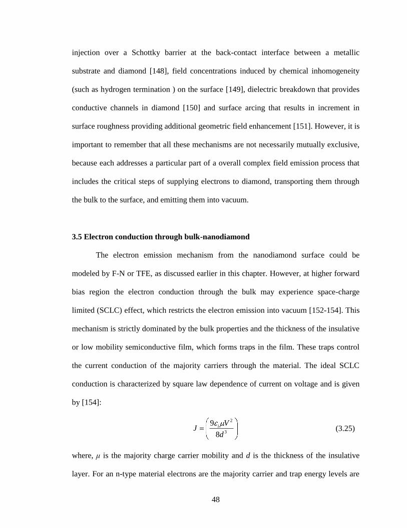
48
injection over a Schottky barrier at the back-contact interface between a metallic
substrate and diamond [148], field concentrations induced by chemical inhomogeneity
(such as hydrogen termination ) on the surface [149], dielectric breakdown that provides
conductive channels in diamond [150] and surface arcing that results in increment in
surface roughness providing additional geometric field enhancement [151]. However, it is
important to remember that all these mechanisms are not necessarily mutually exclusive,
because each addresses a particular part of a overall complex field emission process that
includes the critical steps of supplying electrons to diamond, transporting them through
the bulk to the surface, and emitting them into vacuum.
3.5 Electron conduction through bulk-nanodiamond
The electron emission mechanism from the nanodiamond surface could be
modeled by F-N or TFE, as discussed earlier in this chapter. However, at higher forward
bias region the electron conduction through the bulk may experience space-charge
limited (SCLC) effect, which restricts the electron emission into vacuum [152-154]. This
mechanism is strictly dominated by the bulk properties and the thickness of the insulative
or low mobility semiconductive film, which forms traps in the film. These traps control
the current conduction of the majority carriers through the material. The ideal SCLC
conduction is characterized by square law dependence of current on voltage and is given
by [154]:
2
3
9
8
i VJ
d
(3.25)
where, μ is the majority charge carrier mobility and d is the thickness of the insulative
layer. For an n-type material electrons are the majority carrier and trap energy levels are
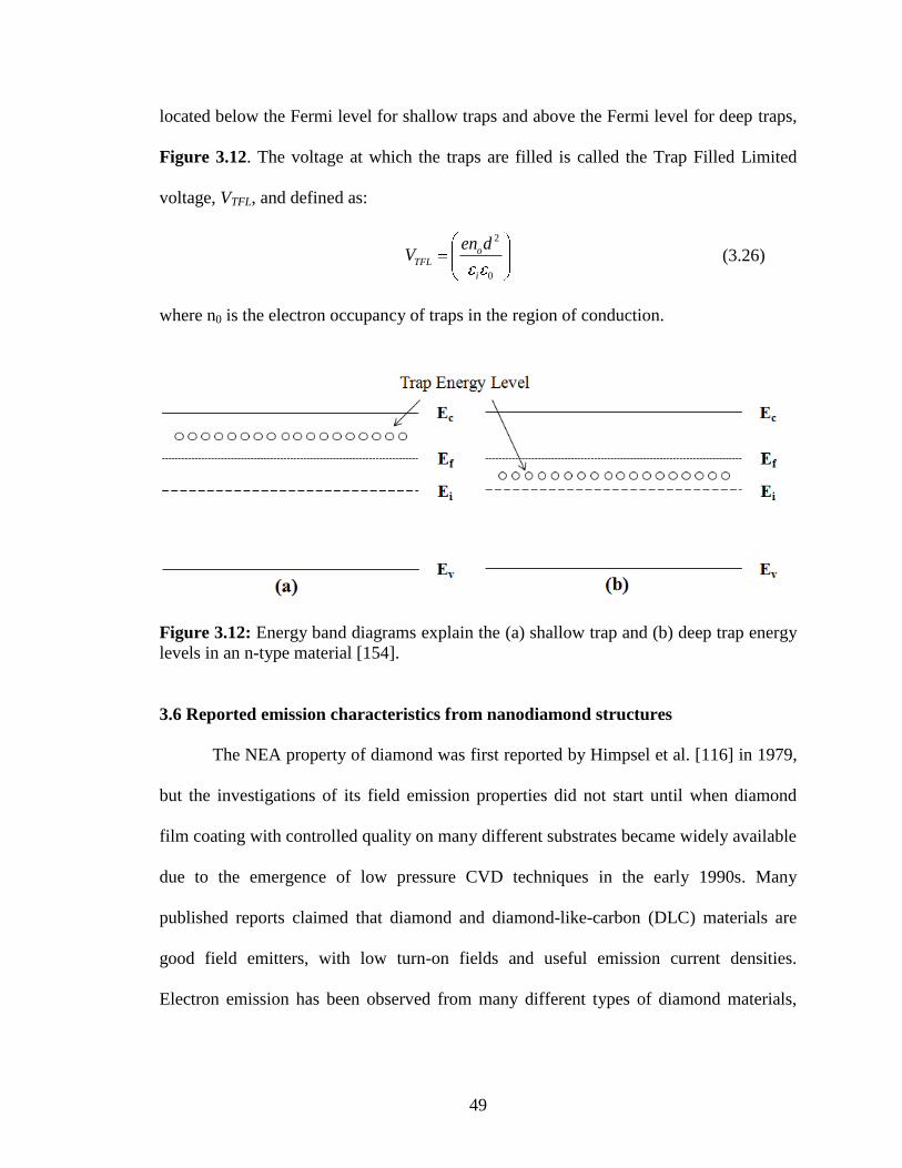
49
located below the Fermi level for shallow traps and above the Fermi level for deep traps,
Figure 3.12. The voltage at which the traps are filled is called the Trap Filled Limited
voltage, VTFL, and defined as:
2
0
oTFL
i
en dV
(3.26)
where n0 is the electron occupancy of traps in the region of conduction.
Figure 3.12: Energy band diagrams explain the (a) shallow trap and (b) deep trap energy
levels in an n-type material [154].
3.6 Reported emission characteristics from nanodiamond structures
The NEA property of diamond was first reported by Himpsel et al. [116] in 1979,
but the investigations of its field emission properties did not start until when diamond
film coating with controlled quality on many different substrates became widely available
due to the emergence of low pressure CVD techniques in the early 1990s. Many
published reports claimed that diamond and diamond-like-carbon (DLC) materials are
good field emitters, with low turn-on fields and useful emission current densities.
Electron emission has been observed from many different types of diamond materials,
50
vapor-deposited islands and films with varying surface morphologies, crystallite sizes
and nanocrystalline coatings [86-102,116-132].
Few of the early reports on diamond field emission include Wang et al. [136] who
reported low-field (< 3 V/µm) electron emission from undoped CVD polycrystalline
diamond films, Geis et al. [128] who measured emission currents from a diamond diode
structure consisting of a p-type & carbon ion implanted diamond surface, and Djubua et
al. [15] who showed that arrays of diamond-like carbon cones formed by plasma
polymerization required the lowest operating voltage for emission when compared to
arrays of Mo and Hf tips. Outstanding emission properties are discovered in both
ultrafine diamond powders containing 1- 20 nm crystallites produced by explosive
synthesis and nanocrystalline or ultra-nanocrystalline diamond films (composed of ~1-
100 nm crystallites) [144,155-158]. Emission has been found to originate from sites that
are associated with defect structures in diamond rather than sharp features on the surface
[136, 158-161]. Compared with conventional Si or metal microtip emitters, diamond
emitters show lower threshold fields, improved emission stability, and robustness in low/
medium vacuum environments. Attempts have also been made to apply diamond
coatings on tips of silicon or metal-emitter arrays to further enhance the emission
characteristics [128, 151].
Nanocrystalline diamond, a strongly emerging form of CVD diamond as an
engineering material, has dominated research in vacuum micro/nanoelectronics in recent
years. Over the last few years Vanderbilt Diamond Group has become one of the leading
research groups in this area and reported emission characteristics from various structures.
A uniquely engineered mold transfer process has been developed for the fabrication of
51
micro-patterned pyramidal diamond emitters with uniform microtip structures. In
addition, methods to improve the diamond field emission behavior have been
systematically studied which include the incorporation of sp2 into diamond tips/bulk,
vacuum-thermal-electric (VTE) treatment, p-type doping, and tip sharpening. Figure
3.13 (a)-(b) shows the SEM micrograph of a high density sharpened diamond tips array
and corresponding field emission behavior [87]. Also, triode and transistor structures
were fabricated and their emission characteristics were studied as a function of the device
parameters of anode-cathode spacing, diamond doping, and array sizes. Figure 3.13 (c)-
(d) shows a typical nanodiamond vertical transistor structure and corresponding electrical
behavior.
Further, optical lithography-controlled finger-like emitter geometry and small
interelectrode spacing in a versatile, low capacitance structure with a built-in gate, anode
and insulator, achieved using a simple fabrication method are attributes of the lateral field
emitter array (FEA) device [86]. Diode structures have been achieved with different
interelectrode spacing. Figure 3.14 shows three diode structures with different numbers
of finger-like emitter and corresponding emission behavior showing that the current
enhancement obtained by increasing the emitter area. Furthermore, vacuum triode and
transistor have also been demonstrated successfully in a completely integrated planar
lateral emitter configuration, as shown in Figure 3.15. Importantly, this had led to the
development of the first vacuum microelectronic technology with operational
temperature immunity (upto 200 C) as well as radiation hardness; tested upto 15 MRad
total doses and 4.4(1013
) neutrons/cm2 level of radiation exposure.

52
However, there are couples of limitations which are preventing the application of
nanodiamond lateral FEDs into microelectronic circuits. Maximum current limit is one of
them. The lateral vacuum triodes and transistors, as mentioned above, demonstrated an
emission current in the range of ~1 µA which is quite low compared to its solid state
counterparts. The current enhancement in the diode structures has been achieved by
increasing the number of emission sights/tips. But it has increased the device area
footprint as well as fabrication complications leading to lesser yield. Further, emission
current has been increased by reducing the interelectrode gap [86]. However, lithography
limitation and other fabrication techniques used in the process put on hold on further
miniaturization.

53
Figure 3.13: (a) SEM micrograph of a high density sharpened diamond tips array, inset
shows the high magnification image; (b) I-V and F-N plots (inset) for different growth
recipes; (c) a typical nanodiamond vertical transistor structure; (d) corresponding dc
characteristics [87].
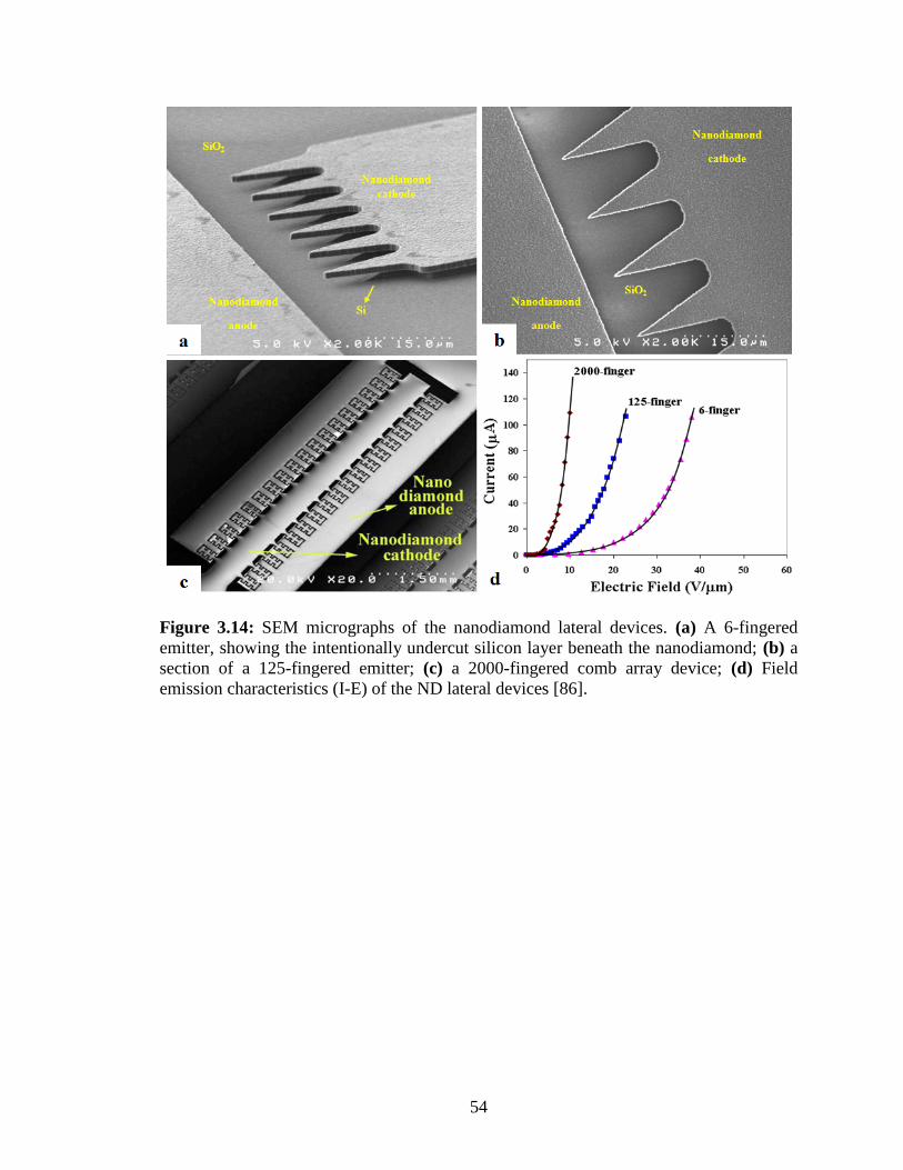
54
Figure 3.14: SEM micrographs of the nanodiamond lateral devices. (a) A 6-fingered
emitter, showing the intentionally undercut silicon layer beneath the nanodiamond; (b) a
section of a 125-fingered emitter; (c) a 2000-fingered comb array device; (d) Field
emission characteristics (I-E) of the ND lateral devices [86].

55
Figure 3.15: (a) SEM micrograph of a completely integrated nanodiamond lateral field
emission triode; (b) corresponding triode characteristics (Ia-Va-Vg) of the one-finger
nanodiamond lateral field emitter device, inset shows F–N plot; (c) monolithic diamond
lateral vacuum transistor; (d) corresponding DC transistor characteristics [86].
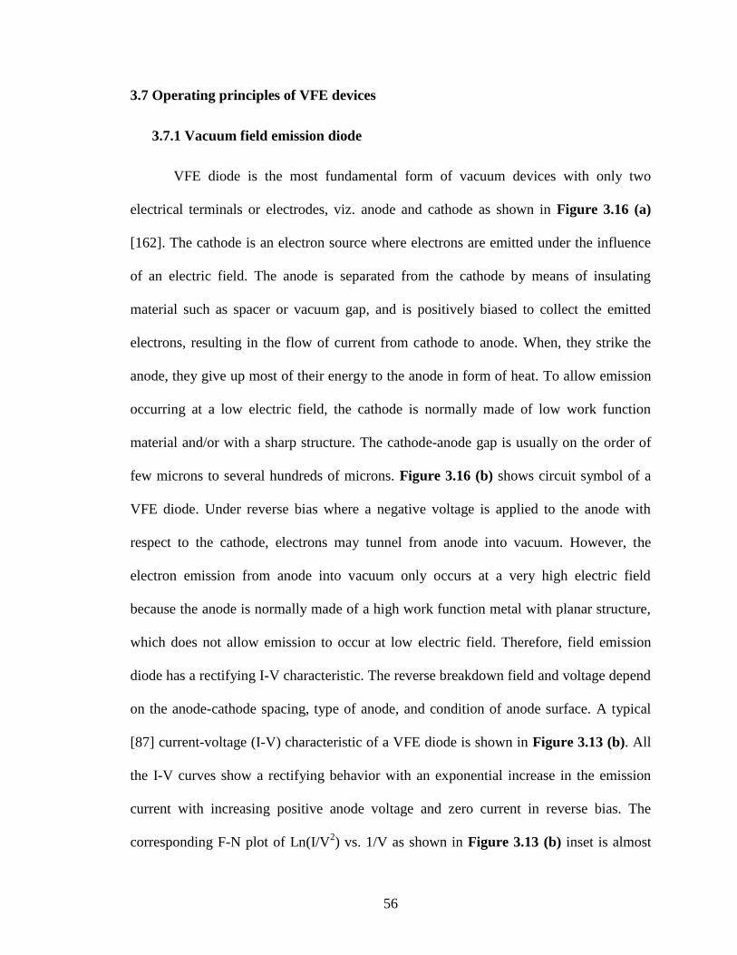
56
3.7 Operating principles of VFE devices
3.7.1 Vacuum field emission diode
VFE diode is the most fundamental form of vacuum devices with only two
electrical terminals or electrodes, viz. anode and cathode as shown in Figure 3.16 (a)
[162]. The cathode is an electron source where electrons are emitted under the influence
of an electric field. The anode is separated from the cathode by means of insulating
material such as spacer or vacuum gap, and is positively biased to collect the emitted
electrons, resulting in the flow of current from cathode to anode. When, they strike the
anode, they give up most of their energy to the anode in form of heat. To allow emission
occurring at a low electric field, the cathode is normally made of low work function
material and/or with a sharp structure. The cathode-anode gap is usually on the order of
few microns to several hundreds of microns. Figure 3.16 (b) shows circuit symbol of a
VFE diode. Under reverse bias where a negative voltage is applied to the anode with
respect to the cathode, electrons may tunnel from anode into vacuum. However, the
electron emission from anode into vacuum only occurs at a very high electric field
because the anode is normally made of a high work function metal with planar structure,
which does not allow emission to occur at low electric field. Therefore, field emission
diode has a rectifying I-V characteristic. The reverse breakdown field and voltage depend
on the anode-cathode spacing, type of anode, and condition of anode surface. A typical
[87] current-voltage (I-V) characteristic of a VFE diode is shown in Figure 3.13 (b). All
the I-V curves show a rectifying behavior with an exponential increase in the emission
current with increasing positive anode voltage and zero current in reverse bias. The
corresponding F-N plot of Ln(I/V2) vs. 1/V as shown in Figure 3.13 (b) inset is almost

57
linear with a negative slope. No deviation due to image and space charge effect can be
observed because the current density is not sufficiently high.
3.7.2 Vacuum field emission triode
Field emission vacuum triode is a three-electrode electronic device, as shown in
Figure 3.16 (c)-(d) [162]. The first two electrodes are cathode and anode as described for
the field emission diode. The third electrode is called grid or gate which is placed
between the cathode and anode in the form of a suitable mesh, screen or circular flat
structure. The emission current flowing from the cathode to the anode must pass through
the gate. Due to the proximity of the gate electrode to the electron-emitting cathode, a
small gate voltage is sufficient to cause a high electric field on the emitter for the
extraction of electrons into vacuum. The gate is, therefore, in a strategic position, and can
largely control the anode current flow. Also, it helps to reduce space charge when
operating in vacuum diode configuration. If the gate is grounded to the cathode, the field
emission behavior of a triode is the same as that of a diode because the gate contributes
no effect on the electric field between anode and cathode. If the gate is made slightly
positive with respect to the cathode, the gate significantly increases the electric field at
the cathode, thus permitting the anode to draw a larger emission current. On the other
hand, if the gate is made negative with respect to the cathode, the negative electric field
of the gate significantly reduces the electric field at the cathode, which results in a
smaller emission current.
A standard thermionic field emission triode normally operates with the gate
voltage made negative with respect to cathode. In this way, cathode-anode current is
controlled by repelling electrons from the gate. On the other hand, the field emission
58
triode normally operates in the opposite regime as the thermionic field emission triode. If
the gate were biased more negative than the cathode, there would be a possibility of
having electron emission from the gate that would create an undesired gate-anode leakage
current. By operating the gate with positive bias, there will be no reverse field emission
from the gate. Under reverse bias where a negative voltage is applied to anode with
respect to cathode at a given gate voltage, there will be no emission current between
anode and cathode until the reverse breakdown voltage is reached where reverse electron
tunneling from anode occurs. Normally, field emission triodes do not operate under these
conditions.
Figure 3.16: (a)-(b) Field emission vacuum diode structure and symbol respectively; (c)-
(d) Field emission vacuum triode structure and symbol respectively [162].

59
Three characteristic coefficients of a vacuum triode
The performance characteristics of a vacuum triode are determined by three
important parameters [87], viz. amplification factor (µ), gate-anode transconductance
(gm), and anode resistance (ra). These three coefficients are particularly useful for ac
equivalent circuit modeling of vacuum triode. First, μ is a measure of the effectiveness of
gate voltage (Vg) in controlling the anode current (Ia). In other words, the amplification
factor is the ratio of a change in anode voltage (Va) to a change in gate voltage at constant
anode current. It is also called static gain. This parameter determines the voltage gain
(Av) of the amplifier for signal amplification applications. Mathematically, it can be
defined as,
constIg
a
a
V
V (3.27)
Next, gm indicates the current driving capability, the voltage gain and high
frequency response of a triode amplifier. It is defined as the change in the anode current
due to a change in the gate voltage at a given anode voltage. It is also called mutual
conductance or simply, transconductance. Mathematically,
constVg
am
a
V
Ig (3.28)
Last, ra measures the effectiveness of anode voltage in controlling anode current
at a certain gate voltage and can be expressed as:
constantg
aa
a V
Vr
I (3.29)

60
The values of μ, gm and ra are not constant, in the strict sense, because these values
vary with the operating conditions. For a given set of conditions, however, a useful
relation exists among these coefficients.
. .a a aa m
a g g
V I Vr g
I V V (3.30)

61
CHAPTER IV
PROPOSED RESEARCH AND APPROACH
4.1 Overview
The purpose of this research is to develop a reliable fabrication process to achieve
efficient monolithic multifinger nanodiamond lateral field emission devices operable at
low voltage with high emission current for vacuum micro/nanoelectronics and IC-
compatible applications. To achieve this goal, the research is classified into two main
sections. First part deals with the study, processing and optimization of the processing
parameters for multilevel electron beam lithography (EBL) and dry etching methods used
in this research to develop well-controlled, highly selective and reproducible processes
for micropatterning of nanodiamond films using thin metal film as masking layer. The
Raith eLiNE EBL tool, Figure 4.1 [163-164], has been used throughout the research for
precise lithography. The following part of the research includes the application of these
developed processes for designing, fabrication and characterization of
micro/nanopatterned nanodiamond lateral field emission devices. Various multi-mask
level fabrication schemes, involving RIE-enabled batch-processing have been
successfully employed to yield nanodiamond lateral field emitter cathodes in sub-micron
gap two-terminal and multifinger three-terminal configurations. The specific device
design, fabrication details, characterization techniques, device behaviors and
experimental results achieved are presented and discussed in chapter V and VI. The
following sections summarize the significance of this research and the adopted approach.

62
Figure 4.1: Raith eLiNE electron beam lithography (EBL) tool [163-164].
4.2 Development of nanodiamond micropatterning technique
As discussed in the previous chapters, nitrogen-incorporated nanocrystalline
diamond is a very promising form of CVD diamond. The nanodiamond growth plasma
chemistry can be effectively controlled to define the grain size, sp2-carbon content, and
the nitrogen n-type conductivity in the thin film. A suitable process technique involving
CH4/H2/N2 microwave plasma-enhanced chemical vapor deposition (MPCVD) to grow
nitrogen-incorporated nanodiamond on silicon-on-insulator (SOI) has been identified.
This nanodiamond film would be utilized for vacuum field emission in different
geometry. Detail growth technique is mentioned in the next chapter.
63
The fabrication method adopted in this research is a subtractive process. Each
additional step that requires selective removal of unwanted materials potentially widens
the pattern. The amount of widening is dependent on the masking material thickness.
Thus, the development of robust micropatterning technique for nanodiamond is essential
to utilize its unique properties and realize useful device structures. Non-uniformity in
diamond emitter microstructures can result in uncontrolled randomly scattered emission
sites, inconsistent emission behavior and no long-term stability. Nanodiamond lateral
devices with micron-range anode-cathode spacing have been reported earlier using
optical lithography [86]. However, minimizing the gap is necessary for achieving sub-
volt turn-on. EBL has been introduced to overcome the conventional photolithography
limitations and to achieve sub-micron gap design requirements. Incorporation of EBL
into the process sequence would make it more complicated and thus, require developing a
new series of recipes which involve the identification of proper photoresist with right
thickness, optimum EBL exposure parameters and appropriate metal masking layer
thickness. Further, nanodiamond etch recipe for the sub-micron gap pattern will be
developed using inductively coupled plasma-reactive ion etch technique (ICP-RIE) in
pure oxygen plasma with good selectivity, etch rate and reproducibility. Experimental
trials involve different etchant gas chemistries, power and pressure, which would
ultimately lead to establish a complete nanodiamond micropatterning process for
fabricating advanced nanodiamond lateral diode and triodes.
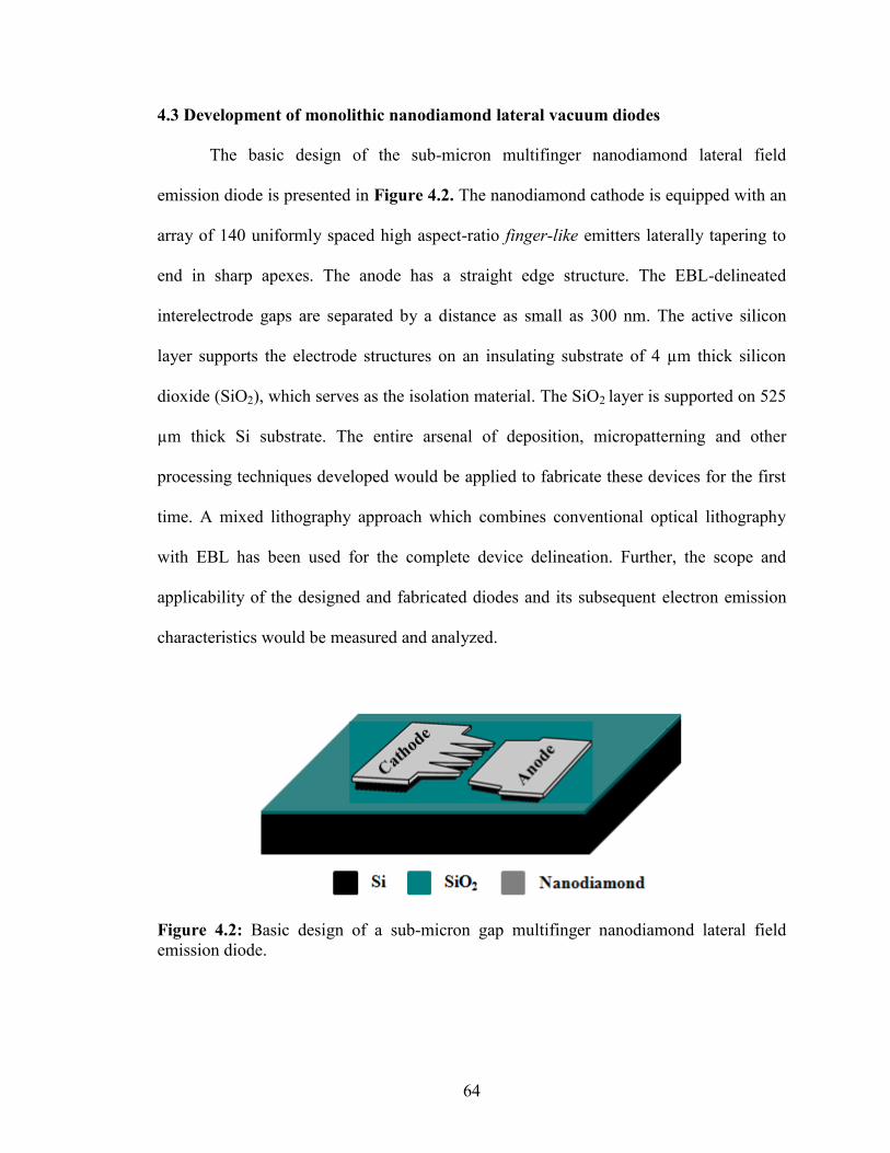
64
4.3 Development of monolithic nanodiamond lateral vacuum diodes
The basic design of the sub-micron multifinger nanodiamond lateral field
emission diode is presented in Figure 4.2. The nanodiamond cathode is equipped with an
array of 140 uniformly spaced high aspect-ratio finger-like emitters laterally tapering to
end in sharp apexes. The anode has a straight edge structure. The EBL-delineated
interelectrode gaps are separated by a distance as small as 300 nm. The active silicon
layer supports the electrode structures on an insulating substrate of 4 µm thick silicon
dioxide (SiO2), which serves as the isolation material. The SiO2 layer is supported on 525
µm thick Si substrate. The entire arsenal of deposition, micropatterning and other
processing techniques developed would be applied to fabricate these devices for the first
time. A mixed lithography approach which combines conventional optical lithography
with EBL has been used for the complete device delineation. Further, the scope and
applicability of the designed and fabricated diodes and its subsequent electron emission
characteristics would be measured and analyzed.
Figure 4.2: Basic design of a sub-micron gap multifinger nanodiamond lateral field
emission diode.

65
4.4 Development of monolithic nanodiamond lateral vacuum triodes
Lateral configuration is one of the best approaches to achieve 3-terminal field
emission devices, as those can be fabricated in monolithic configuration. An important
parameter for vacuum triode design is the emission current modulation by gate voltage.
For most practical applications, the modulating voltage is desired to be small. Similarly
for the diamond vacuum triode, the gate voltage relies on the turn-on electric field of
diamond cathode, the gate-cathode spacing and the number of emission sites. Figure 4.3
represents the multifinger nanodiamond lateral triode design which has never been
realized earlier. The structure is a monolithic field emission device, with 140 efficient
nanodiamond finger-like emitter array as cathode with integrated anode and gate. SOI
wafer has been used as the basic substrate. As expected, the fabrication complicacy has
gone higher with more EBL steps and further etching/lift-off processes. A majority of this
research would be focused on the development of these multifinger nanodiamond lateral
field emission 3-terminal structures owing to its immense potential as a microelectronic
device. To realize the structure, Figure 4.3, a selective portion of the SOI oxide(SiO2)
has to be etched away from under the nanodiamond finger to expose them to the
underneath handling Si. Selection of proper masking material for etching the 4 µm SiO2
has proved to be a challenging task. Next chapter elaborates the fabrication challenges
encountered and their solutions. Later, the electrical performance of the fabricated
devices has to be studied.

66
Figure 4.3 Basic design of a nanodiamond lateral multifinger field emission triode.

67
CHAPTER V
DEVICE FABRICATION, RESULTS and DISCUSSION
A nanodiamond field emission device developed in lateral configuration can
result in efficient low-voltage and high-frequency electronic performance. A lithography-
controlled emitter geometry and small interelectrode separation in a versatile, low
capacitance structure including a built-in anode and insulator are salient attributes of a
lateral field emitter device. By process integration of nitrogen-incorporated nanodiamond
film deposition with the controlled diamond micropatterning technique, multiple lateral
nanodiamond field emitter arrays have been batch-fabricated on SOI wafers, creating a
useful approach to realize potential vacuum electron devices for applications. This
chapter describes the process techniques developed for the nanodiamond material, and
the fabrication schemes for the development of monolithic nanodiamond lateral field
emitter devices, along with experimental results.
5.1 Deposition of nanocrystalline diamond thin-film
In this research, nanocrystalline diamond films were deposited in an ASTeX®
MPCVD system with a 1.5 kW generator, operating at 2.45 GHz. The schematic of a
typical MPCVD system is shown in Figure 5.1 (a). The substrate temperature was set
using an induction heater independent of the plasma. The growth system was coupled
with a controlled gas handling system, allowing precise control of the process gas flow
rates. Since silicon-on-insulator (SOI) wafers (2 μm active Si on 4 µm buried oxide on a
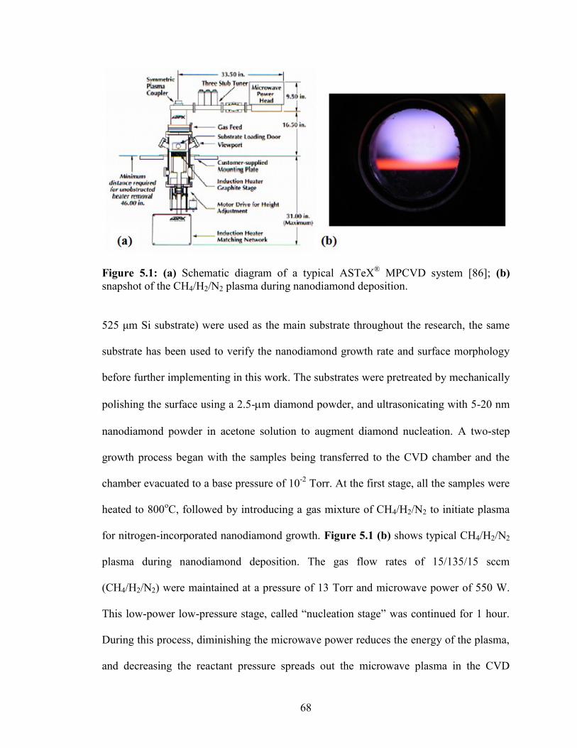
68
Figure 5.1: (a) Schematic diagram of a typical ASTeX®
MPCVD system [86]; (b)
snapshot of the CH4/H2/N2 plasma during nanodiamond deposition.
525 μm Si substrate) were used as the main substrate throughout the research, the same
substrate has been used to verify the nanodiamond growth rate and surface morphology
before further implementing in this work. The substrates were pretreated by mechanically
polishing the surface using a 2.5-m diamond powder, and ultrasonicating with 5-20 nm
nanodiamond powder in acetone solution to augment diamond nucleation. A two-step
growth process began with the samples being transferred to the CVD chamber and the
chamber evacuated to a base pressure of 10-2
Torr. At the first stage, all the samples were
heated to 800oC, followed by introducing a gas mixture of CH4/H2/N2 to initiate plasma
for nitrogen-incorporated nanodiamond growth. Figure 5.1 (b) shows typical CH4/H2/N2
plasma during nanodiamond deposition. The gas flow rates of 15/135/15 sccm
(CH4/H2/N2) were maintained at a pressure of 13 Torr and microwave power of 550 W.
This low-power low-pressure stage, called “nucleation stage” was continued for 1 hour.
During this process, diminishing the microwave power reduces the energy of the plasma,
and decreasing the reactant pressure spreads out the microwave plasma in the CVD
69
growth chamber. Thus the reaction process is starved. Hence, the two events, diamond
nucleation and growth compete against each other for the limited amount of energy
available. In this condition, the nucleation density will increase and the grain size
diminishes [86]. Thus, a high density of nano-sized, fine diamond grains conglomerate
on the substrate to initiate the nanocrystalline diamond film. This growth rate control
process methodology facilitates the synthesis of a very thin, continuous and smooth layer
of CVD nanodiamond. In the next step, viz. ‘growth stage’, to conduct a set of
comprehensive trials, the growth temperature and pressure were varied while the same
gas flow rate and temperature were maintained. Microwave power was increased to 1000
W from 550 W for faster growth rate. This process was continued for another 3 hours.
Table 5.1summerizes the process parameter variation associated with respective samples.
The morphology of the CVD diamond films were examined using a scanning electron
microscope (SEM), while the average grain size was determined by scanning across the
surface of the film. Figure 5.2 shows the set of CVD diamond films that was synthesized
in order to identify a smooth and conductive diamond film for this study. The images
revel that the “Sample d” has the lowest surface roughness compared to the others and
that is why it has been selected for further processing. Figure 5.3 shows the high
magnification and cross-sectional images of the corresponding sample, which clearly
shows the small grain size of 5-10 nm and a thickness of 1-1.2 µm on SOI wafer.

70
Table 5.1: Summery of the process parameter variation associated with respective
samples
Figure 5.2: SEM micrographs of deposited nanocrystalline diamond film grown by
CH4/H2/N2 MPECVD process technique at different conditions as shown in Table 5.1.

71
Figure 5.3: (a) The high magnification SEM of the nanodiamond film to be used in this
research with average grain size of 5-10 nm deposited by CH4/H2/N2 microwave plasma
CVD process; (b) Corresponding cross-sectional view shows the thickness of the film.
The film growth rate was found to be ~0.25 m/hr. The low surface roughness is
extremely important to minimize the photon/electron scattering during lithography;
otherwise it would result into wider device structure. A common method of scratch test
which was used to evaluate the adhesion strength of the nanodiamond film onto the
substrate showed that film has an excellent adhesion to its base. Further, electrical
resistance measurements were performed using a multimeter, probed on identical-sized
gold (Au) circular electrodes on the surface of nanodiamond film. Direct measurement of
the electrical conductivity at room temperature showed that the “Sample d” has a
resistance of 1-10 k. The high electrical conductivity of nanodiamond obtained from
CH4/H2/N2 MPCVD is attributed to the incorporation of nitrogen. Also, the nitrogen
concentration should be uniform throughout the diamond layer because the incorporation
technique is homogeneous throughout thin film deposition. The Increase in electrical
conductivity clearly indicates a decrease in the work function; experimental techniques to
estimate this reduction in the work function of the material form a subject of further
study. The continuity, conductivity and uniformity of this thin film over a 1-inch wafer

72
area were found to be highly suitable for integration into device forms based on previous
studies discussed elsewhere[86]. The grain size has been assumed to be the same
throughout the depth of the diamond film.
5.2 Micropatterning of the nanocrystalline diamond film
One of the reasons for CVD diamond being less utilized as a field emitter is that it
is difficult to pattern diamond films due to the scarcity of appropriate wet or dry etching
techniques. Diamond, being the hardest material, requires a well-controlled etch process
to be patterned uniformly to realize useful structures for varied applications. Lithography
on microcrystalline diamond substrates is also a concern, due to its surface roughness.
With the nanodiamond films developed in this research, having a small grain size and
smooth surface morphology and uniformly controllable thickness, it is possible to
overcome many lithography problems. The Vanderbilt Diamond Laboratory has
previously created a mold transfer and diamond micropatterning technique to generate
topologically managed diamond vacuum field emitters in both lateral and vertical
geometry [86-87]. In this research, first, a reactive ion etch (RIE) nanodiamond
micropatterning process technique is developed using a Trion Phantom II RIE tool, which
has been utilized later in this study in the fabrication of a variety of diamond-based
devices. Next the development of lateral sub-micron gap diode and multifinger triode has
been discussed using EBL.

73
5.2.1 Nanodiamond RIE process development
Reactive ion etching of diamond has been attempted by different research groups
with moderate success. Low etch rate, non-uniform etching, and inadequate mask-defined
selectivity for device-level micropatterning have been some of the issues encountered
during the etching. This research overcomes these concerns to develop a consistent and
well-controlled micropatterning technique and realize potential electron field emitter
structures. Experimentation involving different plasma technology sources, etchant gas
chemistries, power and pressure conditions, and masking materials of varied thicknesses
led to the establishment of the nanodiamond micropatterning process. The utilization of
an ICP-RIE system, based on the inductively-coupled plasma technology combining a
high conductance, high vacuum compatible process chamber with an ICP source to
produce very high ion density at controlled low pressures. Metal used as an etching mask
would protect un-exposed areas on the diamond from being removed. Since aluminum
(Al) did adhere well to the diamond substrate, it was tested as masking material. As
thickness is a critical parameter, for subsequent lateral field emission device processing,
the Al mask thickness was optimized according to diamond film thickness and ND RIE
process parameters as shown in Figure 5.4. Al masking layer of 400 nm thick was found
to offer good selectivity, allowing the micropatterned nanodiamond structures to retain
the beneficial properties of the material. Based on the results, several other modifications
in the fabrication process have been done to avoid problems in future. First, an additional
ultrasonic cleaning in acetone was introduced after ND growth to remove any unwanted
particle or carbon flex from the surface enhancing the smoothness of the ND surface.
These carbon flexes were believed to deposit on the surface from the inside wall of the

74
MPCVD chamber during or after the synthesis. Next, the substrate heating during RIE of
ND has been addressed. Since the RIE tool, Trion Phantom II, does not provide any
substrate holder cooling mechanism, the total etch time has been divided into several
small etching steps and a cooling gas has been introduced into the chamber in between.
Thus each modified ND RIE cycle consists of two steps; Oxygen (O2) plasma etching
followed by surface cooling using carbon tetrafluoride (CF4) without any plasma. CF4 has
been used because of it high thermal conductivity and compatibility with material used in
this process. In wafer-scale fabrication, the developed process scheme can also improve
the processing yield to achieve monolithic emitter devices. The results are demonstrated
in the successive sections with detail process parameters.
Figure 5.4: Cross-sectional SEM of nanodiamond film coated with Al as masking
material; (a) Al thickness during the trial run; (b) Al thickness used throughout this
research.

75
5.2.2 Multifinger micron-gap nanodiamond lateral diodes fabrication
Nitrogen-incorporated nanodiamond films grown by the CH4/H2/N2 MPCVD,
described earlier in this chapter were applied in the fabrication of lateral nanodiamond
array cathodes in four different diode configurations. The physical and electrical
characteristics of the diamond devices have been explored by Subramanian at Vanderbilt
[86]. Although the focus of this research is on submicron-gap diode and multifinger
triode, the micron-gap diode structure obtained by several modifications and its field
emission properties can be evaluated before application in advanced monolithic device
configurations.
The micron-gap nanodiamond lateral field emitter devices were physically
realized using an uncomplicated single-mask fabrication technique using optical
lithography, paralleling conventional IC processing technology. The process schema is
shown in Figure 5.5. The fabrication begins with the growth of a 1-1.2-μm thick
nitrogen-incorporated nanodiamond film on a SOI wafer by CH4/H2/N2 MPECVD. Then
the substrate is ultrasonically cleaned in acetone bath to remove any unwanted particle
from the surface resulting smoother surface. Next, an aluminum metal layer of 400nm
thick is deposited on the nanodiamond by e-beam evaporation. The Al layer is then
patterned with the lateral device structures using optical photolithography, the exposed
aluminum being etched away at room temperature by a commercially available wet
chemical, PAE (80% phosphoric acid-based etchant) and the photoresist removed. With
this aluminum serving as a mask, micropatterning of the nanodiamond film is carried out.
R.F.-assisted pure oxygen plasma chemistry was identified to be a very efficient diamond
etchant. As mentioned earlier, the patterning of ND film using ICP-RIE consists of two

76
steps; etching and subsequent cooling. The beginning of each cycle starts with the ‘etch
step’ which includes a coil R.F. power of 800 W, platen R.F. power of 150 W, oxygen
flow rate of 30 sccm, at a pressure of 10 mTorr. Then, at ‘cooling step’, the gas flow was
stitched to CF4 with flow rate of 100 sccm at a pressure of 300 mTorr. No coil and platen
power was applied during the second step. The etch conditions of high R.F. power and
low pressure helped achieve good anisotropy, the high energy reactive ions with
minimum ion scattering giving a moderate diamond etch rate of ~ 0.2 μm/min and
directionality. The selective etching ratio of diamond against aluminum was found to be
suitably high for device pattern formation. The etching was examined to be uniform over
Figure 5.5: Single-mask fabrication process for the micron-gap nanodiamond lateral
field emission diodes.

77
a reasonably large area, leaving a smooth substrate surface with no residue at the end of
the RIE process, facilitating high-yield batch-fabrication of devices applying
nanodiamond. Finally, a silicon etch step was performed to expose the underlying SiO2
layer of the SOI substrate, which serves as the isolating material. This process step is
performed by using HF:HNO3 solution at room temperature in 1:30 ratio. The wet
etching of active Si layer ensures no plasma damage of the exposed SiO2 surface layer,
which enhance the device performance and life by minimizing possible surface electron
conduction during device operation. Also, this Si layer has intentionally been over-etched
to facilitate electron emission only from the nanodiamond tips. Post-fabrication, the
nanodiamond lateral devices are subjected to RCA chemical cleaning procedure,
followed in the silicon wafer industry standard process technology, to remove any
contaminants present on the emitter surface. Lateral field emission diodes, fabricated
using this nanodiamond micropattern process technique are presented in Figure 5.6-5.7.
The emitters of 125-fingered diodes are designed in a straight line, while 650-, 2000- and
9000-fingered diodes are composed of arrays in comb shape configurations, with each
comb composed of 65 fingers, as shown in Figure 5.8 (b)-(d), with uniform anode-
cathode spacing. The 650-fingered lateral device is composed of two isolated anodes,
325-fingers associated with each, and a common cathode. The large contact pads aid
visual electrical probing. The field emission characteristics of the nanodiamond microtip
array cathodes are reported in the next chapter.
This ensuing section put forward the basic fabrication process schemes developed
for monolithically integrated nanodiamond lateral submicron-gap diode and multifinger
triode with some advancement and alteration in the processing sequences.
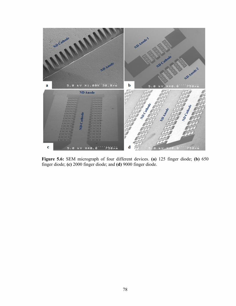
78
Figure 5.6: SEM micrograph of four different devices. (a) 125 finger diode; (b) 650
finger diode; (c) 2000 finger diode; and (d) 9000 finger diode.

79
Figure 5.7: High magnification SEM micrograph of the fabricated devices. (a) 125 finger
diode; (b)-(c) comb shape configurations; and (d) higher magnification of a comb.

80
5.3 Fabrication of multifinger monolithic nanodiamond lateral triode
Nanodiamond lateral triode has also been fabricated using almost the same
process scheme with few additional steps at the end. The monolithic lateral vacuum
microtriode comprises of 140 nanodiamond finger-like structures as emitter with straight
edge nanodiamond pad as 2nd
electrode, and the precisely exposed substrate Si as 3rd
electrode, all on the same substrate. The structure was achieved by control of lithography
and the subsequent subtractive processes. For better understanding, the fabrication
process can be divided into two parts. In the first part, a nanodiamond diode structure has
been obtained with the nanodiamond electrodes sitting on active Si layer, and in the next
part; EBL has been introduced to realize the third electrode.
The first part could have been achieved by optical lithography to accommodate batch
fabrication. The process is performed as mentioned in section 5.2.2, until the active Si
layer etch step, “Step 7” in Figure 5.5. The fabrication schematic for the nanodiamond
triode structures are shown in Figure 5.8. Additionally, upto the diode configuration, the
structure could have been achieved using EBL which is going to be discussed thoroughly
in the next section. The Si layer has been used as a hard mask for the next processing
part. In the following processing steps, after ND etching, e-Resist ZEP 520A is coated on
the surface and a line of dimension 1µm x 1.6mm is drawn along the emitter tips on the
ZEP coated Si layer using e-beam lithography. After developing, the resist is used as
mask to etch the exposed Si. Figure 5.9 shows the SEM images of the device structure
after controlled e-beam writing and selective Si etching. The etching is performed using
the RIE tool as mentioned earlier in this chapter. ZEP 520A has been chosen over PMMA
for its better compatibility for dry etching. Next, the resist is striped-off and oxide etching

81
is performed using the patterned Si as mask. Finally, the device Si layer is removed to
achieve the electrode isolation and standard RCA cleaning procedure is performed to
remove any contaminations. Figure 5.10 shows the final device structure.
Figure 5.8: Mixed lithography fabrication approach schematic for the multifinger
nanodiamond lateral field emission triodes.
Compatibility of diamond films for integration with many other different
materials (semiconductors, metals, oxides) is a requisite for realizing active diamond-
based devices. The development of the planar nanodiamond lateral field emission device
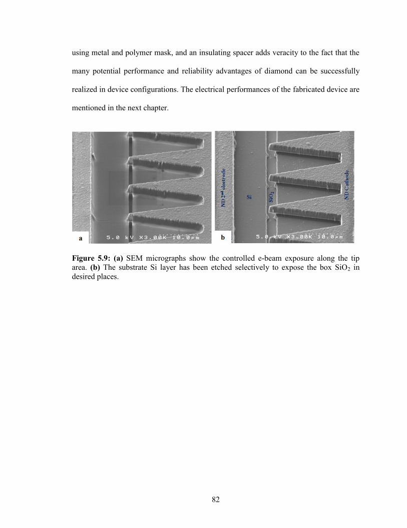
82
using metal and polymer mask, and an insulating spacer adds veracity to the fact that the
many potential performance and reliability advantages of diamond can be successfully
realized in device configurations. The electrical performances of the fabricated device are
mentioned in the next chapter.
Figure 5.9: (a) SEM micrographs show the controlled e-beam exposure along the tip
area. (b) The substrate Si layer has been etched selectively to expose the box SiO2 in
desired places.
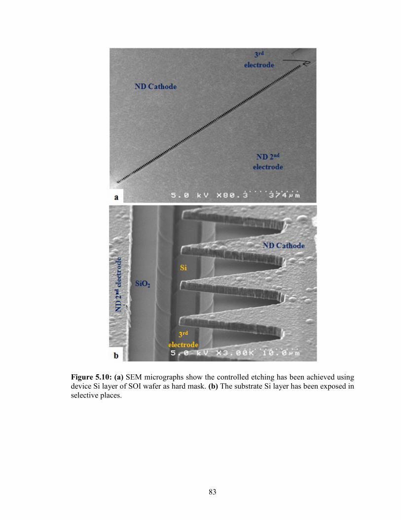
83
Figure 5.10: (a) SEM micrographs show the controlled etching has been achieved using
device Si layer of SOI wafer as hard mask. (b) The substrate Si layer has been exposed in
selective places.

84
5.4 Fabrication of multifinger submicron-gap nanodiamond lateral diode
Decreasing the interelectrode distance is one of the most effective ways to reduce
the turn-on voltage/field of FEDs. Due to the optical lithography resolution, much of the
early research on lateral vacuum FEDs was limited to inter-electrode spacing in the
micron range. Sub-micron spacing would essentially offer high field strength without the
use of high voltage and can be achieved using EBL as proposed in this section. Basically,
E-beam lithography consists of shooting a narrow, concentrated beam of electrons onto
an e-beam sensitive resist coated substrate. This lithography technology is sequential,
which means it write pattern after pattern in a sequence. A combination of self-organized
designs guided by highly sophisticated software is transferred over the surface of a
substrate by scanning the surface using a tightly focused high resolution electron beam.
When the e-beam hits the surface, high energy electron bombardment causes bond
breakage in the resist polymer which then can be used for pattern transfer. Further,
software driven EBL design editor and a pattern generator make the mask design
versatile.
Several important EBL process parameters have been considered for attaining
submicron-gap dimension which include incident beam voltage, dosage, resist thickness
and pattern development time [165]. Higher resolution can be achieved in EBL by using
a very thin resist and a thinner nanodiamond film combination. Thinner films are
preferred since the scattering volume of incident energetic electrons is limited in the
thinner film; scattering effects are reduced as compared with a thicker film. There is also
a delicate balance between the accelerating voltage that would yield a sufficient bore-
through power and result in a tolerable forward and back scattering. A higher

85
accelerating voltage (e.g., 20-40 kV) would give a higher resolution for densely packed
patterns such as the diode structure used in this work. However, back scattered electron
would expose unintended areas, and as a result of the electron scattering from the
proximity effect, the lines in densely patterned areas gets wider than designed. In
contrast, a lower accelerating voltage would offer less scattering, however the beam
resolution deteriorates and designs would be compromised. Another EBL parameter that
requires attention for attaining a sub-micron emission gap is the exposure dose. As a
general rule, the exposure dose increases for decreasing feature sizes. Insufficient dosage
results in shorted devices while over dosage result in wide emission gaps. It can also
induce cross-linking, forming a negative resist. As a result, there will be photoresist
residue on the substrate, while the surrounding area that was exposed positively will wash
away. The EBL written structure is also highly sensitive to development time. E-beam
exposure breaks the e-resist into fragments that are dissolved preferentially by a
developer. Taking all these possible variations into consideration the EBL parameters
have been selected [166] to get the desired structure, which has been discussed next.
The e-beam delineated lateral vacuum diodes comprised of an array of uniformly
spaced, high aspect ratio, 140 finger-like cathode emitters separated by nanometer
distance. The straight-edged integrated anode is isolated by a thick oxide (SiO2) layer
from the emitter giving it the rectifying geometrical field enhancement factor. The
fabrication process mentioned here is based on mixed lithography approach, i.e. using
both optical and e-beam lithography in sequence. The complete fabrication schematic is
presented in Figure 5.10. Upto Al deposition, the approach is same as micron-gap
structure. Then a single-mask conventional lithography is used to delineate the contact

86
pads for both the anode and cathode structures on the AZ 5214E photoresist coated metal
layer. The exposed Al is etched away at room temperature by a wet chemical, PAE and
the photoresist removed. Next, to introduce EBL, a high performance positive e-beam
resist is coated on the substrate surface. ZEP 520A has been chosen due to its high
resolution, high sensitivity and extremely good dry etch resistance. EBL is then used to
delineate the device structure on the e-resist coated Al mask. After developing the
Figure 5.11: Mixed lithography fabrication approach schematic for the multifinger
submicron-gap nanodiamond lateral field emission diodes.
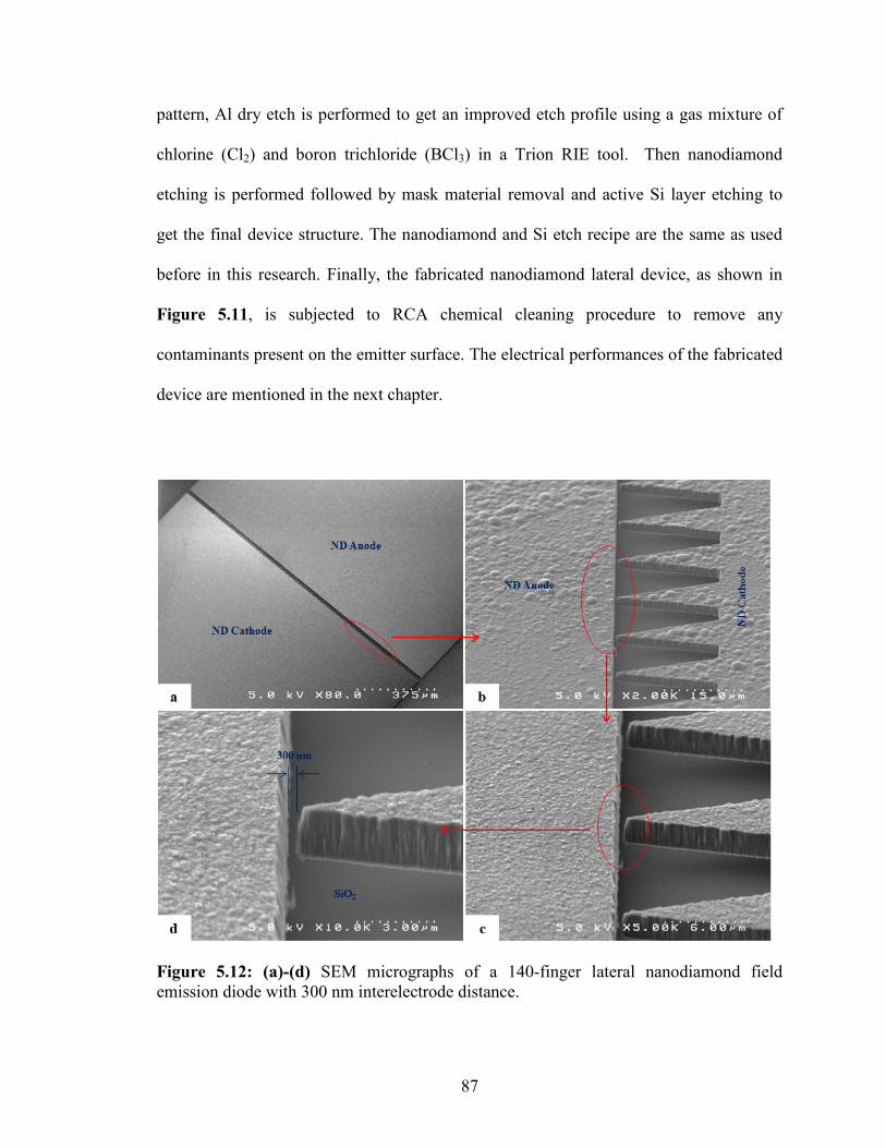
87
pattern, Al dry etch is performed to get an improved etch profile using a gas mixture of
chlorine (Cl2) and boron trichloride (BCl3) in a Trion RIE tool. Then nanodiamond
etching is performed followed by mask material removal and active Si layer etching to
get the final device structure. The nanodiamond and Si etch recipe are the same as used
before in this research. Finally, the fabricated nanodiamond lateral device, as shown in
Figure 5.11, is subjected to RCA chemical cleaning procedure to remove any
contaminants present on the emitter surface. The electrical performances of the fabricated
device are mentioned in the next chapter.
Figure 5.12: (a)-(d) SEM micrographs of a 140-finger lateral nanodiamond field
emission diode with 300 nm interelectrode distance.

88
CHAPTER VI
DEVICE CHARACTERIZATION, RESULTS and DISCUSSION
This chapter outlines the electrical characterization methods employed for the
fabricated nanodiamond devices, viz. diodes and triodes. It also presents and discusses
the electrical performance of these nanodiamond structures under vacuum.
6.1 Device Characterization Techniques
6.1.1 Electron emission characterization of lateral diodes
The electrical performance of lateral diode in vacuum was characterized using the
test set-up shown in Figure 6.1. The fabricated device was maintained in a vacuum
environment of ~10-7
Torr. Flat gold (Au) dots were placed on the contact pads of the
cathode and anode of the lateral device, and were electrically connected to the circuit via
metal probes. The emission current from the nanodiamond fingered emitter cathode was
measured as a function of the applied anode voltage. A continuous power supply, capable
of incrementing the applied voltage in very small intervals was used for low-voltage
characterization of the lateral diodes. Prior to emission characterization, the nanodiamond
lateral device was subjected to in-situ vacuum tip conditioning by means of thermal
desorption to get rid of water vapor or other residual adsorbates on the surface of the
nanodiamond accumulated at the terminus of the emitter device processing or by
exposure to ambient. With the device seated on a heated stage, heat treatment was
performed at 350 C for several hours inside the vacuum chamber. The temperature was

89
measured and controlled by means of a thermocouple feedback at close proximity of the
device. The device was then cooled down slowly to room temperature. Then, without the
application of an external heat source, the nanodiamond lateral emitters were maintained
at a particular emission current, ~10 μA for an hour or more during normal vacuum diode
operation by adjusting the anode voltage, where the extracted field emission current was
used to execute more localized cleaning of the nanodiamond emitter fingertip. The tip
conditioning treatment was terminated when a stable current was obtained for a period of
time. Such post-fabrication conditioning/processing techniques are also common in
conventional silicon IC fabrication technology, such as the rapid thermal annealing
(RTA) treatment performed following an ion implantation step to repair the primary
crystalline damage in the silicon. After the tip conditioning, the I-V characterization of
the nanodiamond lateral diode was performed.
Figure 6.1: Schematic test set-up of the vacuum field emission lateral diode.

90
6.1.2 Field emission characterization of nanodiamond lateral triodes
The testing circuit for emission characteristic of the monolithic lateral vacuum
triode, in a common emitter configuration, is shown in Figure 6.2. Taking the advantage
of the device structure, the device can be operated in two modes of operation by
interchanging the anode and gate. Depending on the mode of operation, a load resistor Ra
in the anode circuit was used to limit the current in the case of short circuit. A resistor Rg
was also used to limit the gate leakage current in the case of short circuit. The anode
emission current was then measured as a function of gate and anode voltages in a vacuum
environment of ~10-7
Torr. The procedures for triode testing were as follows. Initially,
the anode voltage was increased to extract electrons from the cathode, with no gate bias
applied, until a significant anode emission current was perceived. Next, the gate voltage
was altered from zero to apply positive and negative bias and the subsequent anode
current modulation was measured.
Figure 6.2: Schematic test set-up for of the vacuum field emission lateral triode.

91
The anode emission currents versus time were taken by a computer data
acquisition system. For each set of emission current (Ia) measurement, the anode voltage
was scanned manually while keeping the gate voltage constant. The gate voltage was then
changed to a new value and the same emission measurement was repeated until a
complete data set for all gate voltages in the range of interest were attained. The emission
characteristics of triodes were obtained by plotting the anode emission current versus gate
and anode voltages.
6.2 Electrical performance of nanodiamond vacuum electron emitters
6.2.1 Multifinger micron-gap nanodiamond lateral diodes
Each of the nanodiamond lateral devices fabricated in section 5.2.2 were tested
individually in a vacuum chamber, as described earlier, up to an emission current of 60-
50 μA to study the current vs voltage behavior. The 9000-fingered lateral emitters
showed the lowest threshold electric field of ~0.5 V/μm and ~60 μA of emission current
at an electric field of ~3 V/μm or at 12 V. Next, the 2000-fingered lateral emitter was
tested for electrical characterization, which showed threshold electric field of ~1.1 V/μm
and ~58 μA of emission current at an electric field of ~5.5 V/μm or at 22 V. The testing
was followed by the 325-fingered lateral emitter which exhibited a higher threshold field
of ~1.4 V/μm and required ~57 V or an electric field of 14.25 V/μm to generate an
emission current of ~50 μA. Whereas the threshold field of the lateral diodes with 125-
fingered was as high as ~1.5 V/μm and the emission current of ~50 μA was observed at
~19.5 V/μm or at 78 V. The emission current value at the threshold electric field was set
to 10 nA per finger. The current-voltage/field characteristics of these four different

92
Figure 6.3: (a) Field emission characteristics of the nanodiamond lateral diodes in
discussion, showing the current enhancement obtained by increasing the emitter area. (b)
Corresponding Fowler-Nordheim behaviors indicates field emission.

93
devices were shown in Figure 6.3 (a) and the field emission tunneling behaviors were
confirmed by the corresponding linear Fowler-Nordheim plots, Figure 6.3 (b). The F-N
plots of the diodes have almost equal negative slopes, indicating that the work function
(Φ) and field enhancement factor (β) are essentially same for all the four lateral
structures. The slope can be found by taking natural logarithm of Eq. (3.7) and
comparing it with the equation of a straight line, y=mx+c. The observed turn-on electric
field of the nanodiamond lateral emitter is significantly lower than that of comparable
silicon lateral field emitters utilizing an ultra-sharp tip apex, which is typically > 100
V/μm [156-157,167-170]. This is attributed to the superior material properties of
nitrogen-incorporated nanocrystalline diamond offering the diamond emitter diode a
higher effective field enhancement factor or a lower work function than a silicon field
emitter diode. The reported results from silicon lateral field emitters also confirm that for
the electric fields at which the nanodiamond lateral diode operates, there can be no
emission from the silicon layer beneath the nanodiamond fingers. Moreover, the lateral
device processing has been optimized to overetch the Si layer intentionally, as shown in
Figure 5.8 (b), which leaves the silicon having a wider gap distance from the anode and
also with a larger radius of curvature pattern. Further, the active silicon layer of the SOI
substrate was chosen to have a relatively low dopant concentration. All these factors
clearly prove that the emission characteristics of the lateral diode are contributed solely
by nanodiamond.

94
Realizing Logic OR function
Vacuum field emission logic gates have been proposed and simulated before
[171-172], but practical application wasn’t possible because of their design complexity
and high turn-on field. After characterizing individually, three of the four structures, 125-
, 2000- and 9000-fingered diodes, were connected to their identical pair using diode-
resister logic, Figure 6.4 (c), to perform the logical operations [173]. Whereas, utilizing
the structural advantage, only one 650-fingered device was used to realize the same logic.
The 650-fingered lateral device is composed of two identical 325-fingers diodes on a
common cathode with two separately addressable anodes. A square wave from a function
generator was used as the input signal. The input logic low is defined as 0 V and input
logic high is defined separately with a peak to peak amplitude of 18, 10, 7 and 2.2 V for
125-, 325-, 2000 and 9000-fingered lateral structures respectively, in order to maintain
the same output logic high of 1-2 V, and low of 0 V. When the input high was applied to
the anode terminals, A and B, of each pair of similar devices without any time delay, the
output followed the input signal. Next, whenever either of the inputs was set to logic
high, output followed the input. Finally, logic zero was observed at the outputs of each
configuration when both the inputs were set to zero. Oscilloscope images of the Logic
OR behavior under different input configuration for each of the nanodiamond structures
are shown in Figures 6.5-6.8.

95
Figure 6.4: (a) The standard symbol for a two-input OR gate and its Boolean expression;
(b) Corresponding truth table; (c) A diode OR circuit for positive diode-resistor logic,
where V(1), V(0) and V(R) corresponds to logic high, logic low and reference voltage
respectively.

96
Figure 6.5: Oscilloscope images of Logic OR behavior for nanodiamond 125-finger
lateral diodes with 4 μm anode–cathode gap connected in circuit.
Figure 6.6: Oscilloscope images of Logic OR behavior for nanodiamond 325-finger
lateral diodes with 4 μm anode–cathode gap connected in circuit.

97
Figure 6.7: Oscilloscope images of Logic OR behavior for nanodiamond 2000-finger
lateral diodes with 4 μm anode–cathode gap connected in circuit.
Figure 6.8: Oscilloscope images of Logic OR behavior for nanodiamond 9000-finger
lateral diodes with 4 μm anode–cathode gap connected in circuit.

98
Clearly If and only if both the inputs are logic zero, only then the output goes to
zero, otherwise logic one. Hence, these gates correctly perform a logical OR function.
However, while operating in OR configuration, a difference between the input-output
logic highs was observed. Ideally, diodes do not introduce any losses into the circuit
which is not really valid for vacuum diodes and has been explained by theory of field
emission under vacuum at chapter III. It can clearly be noticed that the emission current
may be increased in five different physical ways [86]:
1. Increasing the emission area;
2. Increasing the potential;
3. Field enhancement by tip sharpening;
4. Lowering the emitter work function by doping;
5. Reducing inter electrode spacing.
Earlier in this study we have mentioned the decrease in work function of the
nanodiamond film by incorporating nitrogen in the methane-hydrogen mix during
MPCVD. It is also important to note that the lateral diodes were batch fabricated,
ensuring same work function (Φ), field enhancement factor (β) and inter-electrode
spacing. The F-N plots in Figure 6.3 (b) have almost the same slope values, reconfirms
the above statement. Thus the argumentation of overall emission current capability of the
multi-fingered lateral diodes is attributed to the increase in the emitter area and there by
the number of potential emission sites in the cathode. This clearly explains the current-
field characteristics of the different diodes, Figure 6.3 (a), and hence the mismatch in
input-output logic-high levels for different pairs of structures, Figure 6.9.

99
Figure 6.9: Schematic representation of decrement in input logic highs with increasing
number of emission sites to maintain same output logic high.
Conductivity measurements of the lateral devices in an open-air environment
before and after emission testing were conducted to examine the quality of the silicon
dioxide layer. If the measured current is a leakage current or hopping conduction current
via SiO2, it must remain unchanged in open air as well as in vacuum environments
because leakage and hopping are conduction currents in solid-state devices. However, no
current is observed in open air environment. Therefore, it is sufficient to conclude from
these experimental measurements that the measured current from the micron-gap

100
nanodiamond lateral diodes is indeed the field emission current from nanodiamond
fingers into vacuum.
Half-wave rectification and envelope detection
Further, vacuum microelectronic half-wave rectifier and envelope detector using a
single 2000-fingered nanodiamond lateral field emitter diode with 4 μm interelectrode
spacing have been studied. The diode was connected in a simple diode-resistor circuit
[173], Figure 6.10 (a), to realize the half-wave rectification. In this configuration, current
is allowed to flow only when the diode is forward biased, outputting the positive half of
the signal. The rectification behavior was verified by the oscilloscope images across a
load resistor (R), Figure 6.10 (b). But this pulsating nature of the output voltage makes it
unsuitable as a dc supply for electronic circuit. The simplest way to reduce the variation
is to place a capacitor (C) across the R, Figure 6.10 (c).
Thus, the envelope fading behavior was observed by placing a 1 µF capacitor at
the output in parallel with the 1 MΩ load resistor, Fig 3b. As the rectified output is fed to
the filter circuit; the capacitor charges to the peak of the diode output. Then it discharges
through the load resistor R for almost the entire cycle, until the raising rectified wave
exceeds the capacitor voltage. Then the diode turns on again to charge the capacitor up to
the peak as before and the process repeats by itself. The time constant value, R*C, is
chosen to be much greater than discharge interval to prevent the output voltage decrease
too much during discharge cycle. A 15 V peak-to-peak sine wave from a function
generator was used as an input signal. However, while operating in both the

101
configurations, a difference of ~5.75 V between the input and output highs were observed
which has been explained in the previous section.
Figure 6.10: (a) A basic half-wave rectifier circuit; (b) Oscilloscope images verify the
half-wave rectification; (c) A linear envelope demodulator circuit; (d) Oscilloscope
images verify the envelope detection.

102
6.2.2 Multifinger monolithic nanodiamond lateral triode
Field emitter triodes are important building blocks in the development of high-
speed, temperature- and radiation-immune vacuum microelectronics. Having examined
nanodiamond as a vacuum diode, the research was extended to examine a nanodiamond
triode in lateral configuration. Lateral triodes were developed, utilizing the same
microfabrication tools applied for the lateral diodes as mentioned in the previous chapter.
Then the 3-terminal lateral configurations were tested under vacuum to investigate the
triode characteristics. It was identified that the position of the gates and anode with
respect to the cathode in the device design plays a significant role in determining its
characteristics.
The 140-finger nanodiamond lateral triode with 10 μm spacing between the
nanodiamond electrodes and 8 μm spacing between the nanodiamond finger emitter and
exposed handling Si was characterized for field emission in a common emitter
configuration in a vacuum condition of ~10-7
Torr. The device structure is shown in
Figure 5.9. The circuit schematic of the test setup is shown in Figure 6.2. The device
was operated similar to classical thermionic triode, where the anode was used to turn-on
the cathode which incorporates multiple nanodiamond fingered emitter, while the gates
were employed to modulate the emission from the cathode to the anode. The only
difference in this case is the gate voltage modulates the electric field at the emitter tip and
hence the tunneling probability, whereas in the thermionic triode, the gate controls the
space charge near the emitter. Taking the advantage of the device structure, the triode
was operated in two modes of operation by interchanging the anode and gate.

103
In the first mode of characterization the handling Si was used as anode and the
other nanodiamond electrode as gate. Figure 6.11 (a) displays the triode I-V
characteristics of the nanodiamond lateral vacuum device at room temperature, indicating
that the anode current is effectively controlled with a gate bias; higher applied positive
gate voltages give higher emission current, whereas negative gate voltages suppress the
emission behavior. For each set of emission current (Ia) measurement, the anode voltage
(Va) was scanned manually while keeping the gate voltage (Vg) constant. The gate voltage
was then changed to a new value and the same emission measurement was repeated until
a complete data set for all gate voltages in the range of interest were attained. For
example, a large anode current (Ia) of ~27 μA was obtained at an Anode voltage (Va) of
~60 V, when the gate bias (Vg) was 10 V. On the other hand, when negative 10 V was
applied at the gate, Ia suppressed to ~12 μA at same Va. During this 3-terminal operation,
the resultant potential field at the cathode consists of two components. They are the
potential field produced by the gate and the field provided by the anode. Thus the total
voltage at the cathode (Vt) is given by [86]:
Vt = Vg + γ.Va (6.1)
where γ is is a constant determined by gate construction. It also weakly depends
on the gate and anode voltages. However, the characteristics of the field emission triodes
depend upon many other factors such as gate-cathode spacing, gate-anode spacing, size
and geometry of gate. The total emission current from the cathode is therefore obtained
by putting Vt into the F-N equation, Eq. (3.7), in the place of anode-cathode voltage (V).
The device characteristics were consistent with the modified F-N relationship, Figure
6.11 (b), which confirms that the emission current is due to tunneling mechanism under

104
different applied electric fields. γ has been calculated by finding the amplification factor
(µ), Eq. (3.27), from the I-V curves. By performing partial differentiation according to
the definition in Eq. (3.7), µ of a field emission triode can be shown equal to γ-1
. Further,
the transconductance parameter (gm), Eq. (3.28), was determined to be ~0.75 µS at Va =
60 V.
In the second mode of operation the handling Si was used as gate and the other
nanodiamond electrode as anode, while keeping the cathode fixed. Figure 6.12 (a)
displays the triode I-V characteristics of the nanodiamond lateral vacuum device at room
temperature, indicating that the anode current was effectively controlled by gate bias. A
larger anode current (Ia) of ~40 μA was obtained at an Anode voltage (Va) of ~60 V,
when the gate bias (Vg) was 10 V. Whereas, negative 10 V at the gate, suppressed Ia to
~20 μA at same Va. It is believed that the higher current attributes to the position of the
gate which is 2 μm closer than the previous case. The total cathode voltage (Vt) was
calculated as earlier case and the device characteristics were also found to follow the
accordingly modified F-N relationship, Figure 6.12 (b), confirming that the measured
anode current is due to the field emission mechanism. Further, the transconductance
parameter (gm) was calculated to be ~0.85, which is one of the highest reported for lateral
device, especially with cathode-gate separation in microns. It is also important to mention
here that the gate-intercepted current must be small relative to the anode current for
optimum performance of the device as triode. As observed in both the cases, the gate
current (Ig) for this lateral triode was below 1μA at the moderate positive gate voltage
(Vg). Furthermore, the emission behavior of the lateral triode was found to be very stable,
e.g. at 45 V, around 13 μA, of current was measured with 2% of fluctuations,

105
Figure 6.11: (a) Triode emission characteristics of the nanodiamond lateral device
operating in mode-1 (handling Si as anode); (b) Corresponding F-N plots are calculated
by taking Vt into consideration.
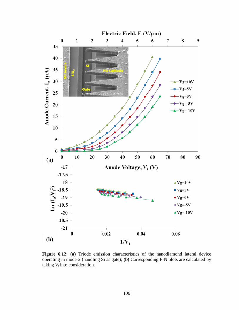
106
Figure 6.12: (a) Triode emission characteristics of the nanodiamond lateral device
operating in mode-2 (handling Si as gate); (b) Corresponding F-N plots are calculated by
taking Vt into consideration.

107
as shown in Figure 6.13. A total of 18x103 data points were collected over the time
period of 10 hours at an equal time interval. While collecting the data, the diode
configuration was achieved by shorting both the interchangeable electrodes and used as a
single anode.
Figure 6.13: The emission behavior of the lateral triode was found to be very stable. For
example, at 45V, applied to both anode and gate, Ia was found to be 13 μA over a time
period of 10 hours’ time with 2% fluctuation.

108
6.2.3 Multifinger submicron-gap nanodiamond lateral diode
The lateral construct provides latitude for further reduction of the device
operating voltage by realizing sub-micron interelectrode spacing with advanced e-beam
lithography. In this section, the electrical characteristics of the fabricated 140-finger
vacuum diode with 300 nm anode-cathode spacing have been reported. Other than SEM
observation, the isolation between the electrodes, as shown in Figure 5.11, has been
verified by electrical resistance measurement using a multimeter on two nanodiamond
contact pads. It was found to be open (> 500 MΩ). The circuit schematic of the test setup
is shown in Figure 6.1. Prior to emission characterization, the nanodiamond lateral
device was subjected to in-situ tip conditioning, as mentioned in section 6.1.1. At room
temperature (270C) the lateral emitter showed the lowest threshold voltage of ~1 V and
0.95 mA of emission current at ~29 V (97 V/μm). Next, the substrate temperature has
increased subsequently to get different sets of I-V characteristics. It has been observed
that the emission currents have increased to 0.98 mA at 1000C and 1 mA at 200
0C at
equivalent electric field. Figure 6.14 (a) shows the corresponding I-V characteristics. The
effective voltage has been obtained by subtracting voltage drop across Ra from the
applied voltage (Va). The emission current from the structure was allowed to stabilize
over a period at different electric fields. Figure 6.14 (b) shows the stable emission
current of 5, 10 and 15 µA with little fluctuation at 8.31 V/µm, 9.86 V/µm and 11.21
V/µm respectively; a total of 3600 data points were collected by a computerized data
acquisition system for every current value at every second.

109
Figure 6.14: (a) I-V characteristics of the fabricated 140-finger diode with 300 nm
anode-cathode distance at different temperature; (b) Stable emission current of 5, 10 and
15 µA with little fluctuation at 8.31 V/µm, 9.86 V/µm and 11.21 V/µm respectively.

110
Previously we have observed that the field emission from micron-gap ND lateral
structures, Figures 5.6-5.7, is governed by F-N equation, Figure 6.3. However, the
submicron gap structure showed a significant divergence from the F-N plot at higher field
region (> ~20 V/μm), as shown in Figure 6.15 (a). So it has become extremely important
to study other possible conduction mechanisms for the 300 nm gap structure. The
expected I-V relations for some of these conduction models are given in Table 6.1,
indicating that a straight line can be obtained by plotting the appropriate mathematical
form of these relations as abscissa and ordinate. The coefficient of determination (r2)
gives a direct measure of how well each model fits the experimental data [174]; provided
the direction and value of the slope has been satisfied. As seen in the F-N plot at room
temperature, Figure 6.15 (a); it can be divided in three distinct regions. In other words,
each region of operation is dominated by different emission mechanisms. Data fitting into
six different mathematical models suggest that at lower field (E < 20 V/μm), electron
emission follows F-N equation which is then followed by space-charge limited
conduction (SCLC) [175-176] at moderate field (20 V/μm < E < 40 V/μm) and finally at
higher field (E > 40 V/μm) thermal-field emission (TFE) [106] dominates. Figure 6.15
clearly represents those three different areas. Figure 6.16-6.18 shows the data fitting into
each of the emission models mentioned in Table 1. Table 6.2 summaries the coefficient
of determination (r2) value of the analysis at different temperature and over the entire
applied electric field.

111

112
Figure 6.15: Three different mechanisms dominate the electron emission. At lower field
(E < 20 V/μm), it follows F-N equation which is then followed by space-charge limited
conduction (SCLC) at moderate field (20 V/μm < E < 40 V/μm) and finally at higher
field (E > 40 V/μm) thermal-field emission (TFE) model dominates.
Table 6.1: The most common mechanisms of electron conduction, their expected
current-voltage relations and mathematical relations required for a straight line plot [106,
175-176].
where, a = k2ɸ
3/2d/β ; k2 = constant; b = (e/4πdεi)
1/2 ; c = (kTt/8π
3)1/2
; c’ = ϴ/24(kT)3 ;
ϴ = 3t-2
-2vt-3
; t & v = parabolic function; b’ = 0.89e3/2
/(πdεi)1/2
*Theoretical slope value = 2

113
Figure 6.16: Fitting the obtained data, upto 20 V/µm, in different mathematical models
as mentioned in Table 6.1. (a) Field Emission, best r2 value with negative slope; (b)
Space-Charge Limited Conduction, slope value > 2; (c) Thermal Field Emission, poorer
r2 value; (d) Transition Region, not a straight line fit; (e) Frenkel-Poole conduction, not a
straight line fit; (f) Space-Charge Limited Conduction with Frenkel-Poole effect, worst r2
value.

114
Figure 6.17: Fitting the obtained data, from 20 V/µm to 40 V/µm, in different
mathematical models as mentioned in Table 6.1. (a) Field Emission, mismatch in slope
direction; (b) Space-Charge Limited Conduction, best r2 value with slope ~2; (c) Thermal
Field Emission, poorer r2 value; (d) Transition Region, not a straight line fit; (e) Frenkel-
Poole conduction, not a straight line fit; (f) Space-Charge Limited Conduction with
Frenkel-Poole effect, mismatch in slope direction.

115
Figure 6.18: Fitting the obtained data, beyond 40 V/µm, in different mathematical
models as mentioned in Table 6.1. (a) Field Emission, mismatch in slope direction; (b)
Space-Charge Limited Conduction, slope value < 2; (c) Thermal Field Emission, best r2
value; (d) Transition Region, not a straight line fit; (e) Frenkel-Poole conduction,
mismatch in slope direction; (f) Space-Charge Limited Conduction with Frenkel-Poole
effect, mismatch in slope direction.

116
Table 6.2 The coefficient of determination (r2) for the straight lines of best fit for
different data plots given at Table 1. (BOLD digits indicate best fit)
A possible explanation for the above observation can be made using a cascaded
Metal-Insulator-Metal (MIM) energy band diagram for the n-type nanocrystalline
diamond film [177-178] with localized shallow trap level lying below the conduction
band, as shown in Figure 6.19. For simplicity, the figure has been drawn by assuming
equal grain size throughout the film. It has also been assumed that the trap density (Nt) is
quite uniformly distributed throughout the film and initially, the trap levels remain
partially occupied [154] under thermal equilibrium without external biasing or any other
forms of stimulation. At lower field, neglecting the effect of image charge, the cascaded
MIM (metal sp2
- insulator sp3
- metal sp2) structure, Figure 6.19 (a), forms a conduction

117
channel consists of sp2 floating particles allowing electrons to tunnel through sp
3-
diamond [135,179-180]. A voltage drop, ΔV appears across each grain or sp3 particle. In
this forward bias region, since the amount of excess majority carrier (electron)
concentration in the conduction band is less, the trap level remains partially occupied
which causes negligible effect on the tunneling electrons. Thus, the emission behavior
obeys F-N model with negative slope, given by Eq. (3.17).
As the bias increases, the trap in the insulative layer (sp3) will capture more and
thereby, immobilize most of the injected electrons [103]. The rate at which this capture
process occurs is proportional to the density of electrons in the conduction band (n), the
density of empty localized state, the probability that an electron passes near a state and is
captured by the state [181]. Thus, the capture rate (r) can be written as:
[ {1 ( )}]t t th nr n N f E v (6.1)
where f(Et) is the probability that the traps are occupied. The product of electron thermal
velocity (vth) and capture cross section (σn) gives the probability that an electron is
captured by a localized trap. Thus, during this period of forward bias, the data points start
to divert from the F-N plot and a square law dependence is observed, which is also
known as SCLC conduction [175-176,182-183]. At this point the trap level is completely
filled with electrons. The MIM energy band diagram of this region of the forward bias is
shown in Figure 6.19 (b). The voltage drop across each grain is higher than the previous
case, i.e. ΔV’>ΔV. If the localized trap charge is an appreciable fraction of the total
charge in the material, it applies a considerable repulsive force on the tunneling electrons.
This lowers the drift mobility and further reduces the free carrier concentration in
conduction band near the surface [154]. Thus the electron emission is limited by the

118
availability of the majority carriers at the surface. The SCLC expression is described in
Eq. (3.25). Further, the theoretical slope of SCLC model is found to be ‘two’ by taking
natural logarithm on both sides of the governing equation and comparing it with an
equation of a straight line. In this region, the calculated slope value based on
mathematical analysis of the experimental data justifies the physical phenomenon,
Figure 6.15 (b). Also, it is believed that the image charge effect can be observed in this
region of operation [7], which results in a small barrier height reduction (ΔΦB1). The
barrier height can be calculated as mentioned earlier in Section 3.3.
As the bias has increased further, more electrons tunnel into vacuum from the
emitting diamond surface. It is believed that, this high volume of electrons’ extraction
from very small cathode tip area causes localized tip heating and has been explained
earlier, in Section 3.3. Thus, by absorbing the available additional heat energy, the
electrons tunnel into vacuum from higher energy state (Ec+ΔE), as shown in Figure 6.19
(c). The emission current associated with this phenomenon is called Thermal-Field
Emission (TFE), which is given by Eq. (3.19). The data fitting to the TFE model strongly
support the physical explanation, as shown in Figure 6.15 (c) [184-185]. However, in the
bulk, the electron transport is still limited by the space-charge and the voltage drop across
each grain is higher than the previous two cases, i.e. ΔV’’>ΔV’>ΔV. Also at this high field
forward bias region, due to the increased image charge density, the barrier height reduces
further (ΔΦB2), i.e. ΔΦB2 > ΔΦB1. Furthermore, at high field region, an increase in
substrate temperature by an external heater alters the total amount of charge in the
conduction band of nanodiamond [186]. The additional thermal energy provides the
trapped electrons the energy required to make a transition to the conduction band. This
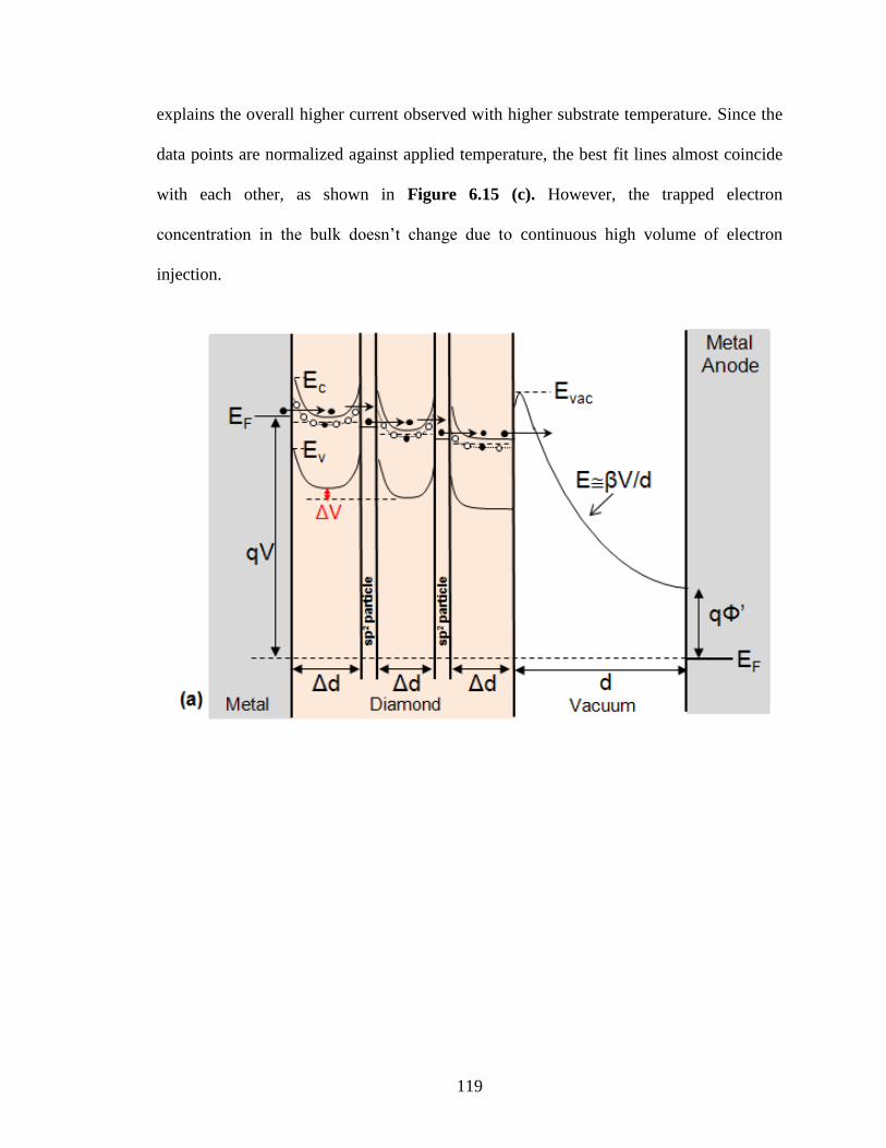
119
explains the overall higher current observed with higher substrate temperature. Since the
data points are normalized against applied temperature, the best fit lines almost coincide
with each other, as shown in Figure 6.15 (c). However, the trapped electron
concentration in the bulk doesn’t change due to continuous high volume of electron
injection.

120
Figure 6.19: Energy band diagrams explain the three different emission mechanisms.
With the higher applied field the Fermi level moves up, i.e. qV<qV’<qV’’ and the voltage
drops inside the film increases, i.e. ΔV<ΔV’<ΔV’’. Also, the barrier height lowering due
to image charge at higher field is more, i.e. ΔΦ2>ΔΦ1. (a) Electron emission governed by
F-N at low field; (b) SCLC mechanism at moderate field; and (c) TFE at higher field; the
additional energy ΔE is provided by internal tip heating.

121
Lateral 3-terminal array devices for performance enhancement – preliminary
investigation for future work
An advance lateral emitter triode array can be developed in future to improve the
performance of the existing triode leading to the transistor structure. It has been shown
earlier in this research that the position of the electrodes play a critical role in
determining the characteristics of the devices. The current scaling behavior of the
nanodiamond lateral field emitters has been demonstrated by other researchers [86-87].
Increasing the cathode area and decreasing the interelectrode gap with uniformly
micropatterned arrays of fingers will lower the operating electric field and voltage and
enhance the current, resulting in increased transconductance suitable for achieving high
signal gain from the triode device, when operated as an amplifier. Since, in the present
structure the gate-cathode gap is in microns, a structural change in the lateral triode
design is required to achieve an enhanced device characteristic.
Figure 6.20 shows the proposed change in the design of the electrodes. The
monolithic structure is composed of an array of nanodiamond lateral finger-like emitters
with metal gate pads at the same plane of the cathode and placed in between the fingers.
All the gate pads are connected by a metal line placed on top of the box oxide. The
device can be fabricated using the multilevel mixed lithography processes developed in
this research. The nanodiamond cathode and anode can be micropatterned by optical
lithography and reactive ion-etch. The gate electrode design can then be transferred onto
the structure by electron-beam lithography followed by gate metal evaporation. During
this research the process flow has been tried but the structure has not been successfully
realized due to various factors. Figure 6.21 shows some of the SEM images captured

122
during processing. Figure 6.21 (c)-(d) shows the desired defect free area of the structure.
However, strategically placed gate formation and metal line melting/peel-off were the
two major concerns at that time. By fine tuning the process parameters and using more
advanced dry etching process and tools, the realization the structure is highly possible.
The distance between the anode and cathode can easily be varied by using proper mask,
while the design and separation of the gate can be controlled by e-beam lithography. It is
believed that, for anode-cathode distance (d) greater than 100 µm, transistor responses
can be observed [86]. Further, to improve the electrical behavior, the metal lines in front
of the emitting tips can be coated by insulating films which will reduce gate intercepted
current.
Figure 6.20: Proposed microstructure for the nanodiamond vacuum lateral emitter array
three-terminal devices with 3-D gate.
Another advance design can be proposed to achieve the transistor performance.
The structure can be built from the current triode structure, as shown in Figure 6.22(b).
The fabrication steps are very similar to the current structure, except an additional deep
Si etching has to be performed to remove handling Si from the exposed trenches
underneath the nanodiamond finger tips. This will allow moving the anode further away
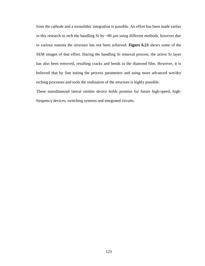
123
from the cathode and a monolithic integration is possible. An effort has been made earlier
in this research to etch the handling Si by ~80 µm using different methods, however due
to various reasons the structure has not been achieved. Figure 6.23 shows some of the
SEM images of that effort. During the handling Si removal process, the active Si layer
has also been removed, resulting cracks and bends in the diamond film. However, it is
believed that by fine tuning the process parameters and using more advanced wet/dry
etching processes and tools the realization of the structure is highly possible.
These nanodiamond lateral emitter device holds promise for future high-speed, high-
frequency devices, switching systems and integrated circuits.

124
Figure 6.21: Few SEM images of the nanodiamond lateral emitter array vacuum three-
terminal devices with 3-D gate. (a) After pattern transfer on nanodiamond and
development; (b) Al coating to form metal lines (before ZEP520A lift-off); (c) Top view
of a defect free area; (d) High-magnification inclined view; (e)-(f) Discontinuous metal
line.

125
Figure 6.22: (a) Present design of a nanodiamond lateral multifinger field emission
transistor; (b) Proposed microstructure for the nanodiamond lateral emitter array vacuum
three-terminal devices with deeper anode.
Figure 6.23: SEM images of the nanodiamond lateral emitter array vacuum three-
terminal devices shows that un-optimized handling Si etching resulted in cracks and
bending in the diamond film.

126
CHAPTER VII
CONCLUSIONS AND RECOMMENDATIONS
In this dissertation, nanocrystalline diamond has been developed as an applicable
microelectronic material. Thin film fabrication processes have been identified for
nitrogen-incorporated nanodiamond and integrated for device fabrication for utilization in
vacuum field emission microelectronics (VFEM). The central idea of this development is
to built and characterize monolithic submicron gap nanodiamond diode and multifinger
triode devices in lateral emitter configuration, demonstrating enhanced electron emission
characteristics at low turn-on voltage and electric field, high and stable emission current,
operational temperature and radiation tolerance, making them potential candidates for
realizing IC-compatible high-speed, high-power, extreme environment electronics,
sensors, and nanoelectromechanical systems (NEMS). In this chapter, the findings from
the experimental works are summarized followed by recommendations for future studies
on lateral vacuum field emission device technology.
7.1 Nanodiamond thin film deposition for lateral device application
Before arriving to the actual device fabrication step, a controlled and consistent
process techniques have been developed to deposit and micropattern nanocrystalline
diamond thin films with properties favorable for vacuum field emission. Factors
contributing to electron field emission from diamond were identified and a suitable form
of the material offering these field enhancement factors realized. An effective growth-rate

127
control method has been obtained and implemented to deposit nanodiamond films with
grain size less than 20 nm and lower surface roughness. Throughout the process
CH4/H2/N2 gas combination was used in a microwave plasma-enhanced chemical vapor
deposition (MPCVD) system. Nitrogen, a suitable n-type dopant in nanocrystalline
diamond films, has been incorporated successfully to realize high electrical conductivity
at room temperature and thereby enhanced electron transport and electron emission
properties. To apply nanodiamond as an efficient electron emitter, a micropatterning
process was developed to derive geometrical field enhancement. The difficulty in
patterning diamond films to build micron/submicron scale devices, has been resolved by
the development of a highly selective and uniform nanodiamond etch process using an
oxygen plasma reactive ion etch (RIE) technique. A high diamond etch rate of ~0.2
µm/min was achieved, and various electron field emitter micro/nanostructures of
nanodiamond realized. Further, a process flow, compatible with conventional
semiconductor integrated circuit (IC) process technology and integration, has been
developed to fabricate nanodiamond lateral field emitter devices on a SOI wafer.
7.2 Nanodiamond lateral Micron-gap diode fabrication and characterization
Monolithic lateral micron gap diodes in chip-type architecture were consistently
batch-processed on silicon-on-insulator (SOI) wafers using a single mask. The deposition
and micropatterning techniques developed for nanodiamond were applied with precise
lithography processing to yield this lateral device features. High aspect-ratio finger-like
nanodiamond lateral emitters as cathode, with a nanodiamond edge structure as anode
was achieved. These lateral diodes were designed with different numbers of emitters,

128
viz., 125, 325, 2000 and 9000, and with equal anode–cathode spacing, ranging from 4-10
µm by design. The emitters of 125-fingered diodes were put in a straight line, while 650-,
2340- and 9360-fingered diodes were composed of arrays in comb shape configurations,
with each comb composed of 65 fingers. Upon completion of the fabrication step, several
aspects of the field emission behavior of the nanodiamond lateral micron-gap diodes were
investigated. A low turn-on voltage of 2.2 V had been achieved from the highest number
of emitter structure. Further, a vacuum logic OR gate had been realized successfully for
the first time using these lateral nanodiamond field emission diodes. The current scaling
phenomenon had been proven to occur from the increase in emission area, i.e. the
increase in number of potential emission sites in the cathode which directly affects the
amplitude of the input signal required to maintain the same output logic for different pairs
of logic OR gates. Furthermore, half-wave rectifier and envelope detector had been
realized using one of the lateral nanodiamond field emission diodes which incorporate
uniformly micropatterned nanodiamond lateral fingers in a comb-array structure at the
cathode geometry. The approach demonstrates a new way of developing temperature- and
radiation-tolerant logic circuits for integrated vacuum microelectronics.
7.3 Nanodiamond lateral multifinger triode fabrication and characterization
The same nanodiamond film was applied to build monolithic lateral vacuum
triodes, with the lateral cathode, gate, and anode integrated on the same substrate.
Advanced micropatterning techniques had been developed with precise lithography
processing to yield this multifinger three-terminal structure for the first time. The anode
can induce the electron emission and result in gate-modulated triode characteristics.

129
Taking the advantage of the device structure, the triode was operated in two modes of
operation by interchanging the anode and gate. A large anode current (Ia) in the range of
27-40 μA was obtained with the transconductance parameter (gm) calculated to be ~0.85
µS, which is one of the highest reported for lateral device, especially with cathode-gate
separation in microns. However, it was identified that the behavior of the lateral emitter
device can be varied by altering the distances between the 3-terminals. Further, negligible
gate leakage current attributes for reliable applications.
7.4 Nanodiamond lateral Submicron-gap diode fabrication and characterization
Reducing the inter-electrode spacing to the sub-micron range offers whole new
and exciting opportunities for nanodiamond lateral device applications, such as lower
operating voltage. After identifying a conductive nanodiamond film with smooth surface,
work was conducted to incorporate electron beam lithography in the fabrication process
and development of sub-micron gap nanodiamond lateral device technology. The micron
gap lateral devices were limited by the resolution capability of traditional optical
lithography. In this part of the work, 140-finger nanodiamond lateral vacuum diode with
300 nm anode-cathode distances was fabricated for the first time using multilevel-mixed-
lithography, which includes optical and electron beam (EBL) lithography. Lower turn-on
with higher stable emission current had been noticed. Further, the possible electron
emission mechanism models were identified and verified by fitting the data to different
emission models. It was observed that the diode’s region of operation is dominated by
three different emission mechanisms. Data fitting into six different mathematical models
suggest that at lower field, electron emission follows Fowler-Nordheim (F-N) equation
130
which is then followed by space-charge limited conduction (SCLC) at moderate field and
finally at higher field, thermal-field emission (TFE) dominates. The coefficient of
determination (r2) of the line of best fit, direction of the slope and its magnitude provided
a direct measure of how well each model fits the experimental data. The behaviors have
been successfully explained using electron energy band diagram.
The emission characteristics of the nanodiamond lateral devices were observed to
be stable and repeatable over time. Low current fluctuations of less than 2% were
observed in the µA emission current regime, which increased slightly at high currents
(mA regime), operating in a vacuum condition of ~10-7
Torr. Further improvement in the
current stability behavior of the diamond lateral emitters can be expected at very low
pressure levels of 10-9
-10-11
Torr. Nevertheless, the ability of the diamond emitter to
function with good stability even at medium pressure levels was noticed. Overall,
nanocrystalline diamond is a favorable material for electron field emission, with its
properties well suited for use in a broad range of applications. With the emergence of
nanodiamond, the utility of CVD diamond can now be vastly expanded to perpetuate the
development of robust devices and products from the material. One such application is
explored in this research in the form of lateral vacuum field emission microelectronics.
The nanodiamond lateral emitter device represents a new category of diamond-based
electronics, made possible from the development of a consistent microfabrication process
capable of achieving desirable micro/nanostructures from the material. The potential
demonstrated by the developed monolithic nanodiamond lateral field emitter diode and
triode devices signify an efficient approach to accomplish rugged integrated circuits (ICs)

131
and electronic systems for terrestrial as well as space-based applications, offering much
higher operational limits, in the near future.
132
7.5 Recommendations for future work
Advanced future research works on the nanodiamond lateral vacuum
microelectronic devices, can be summarized in the form of following investigations:
(i) Design, simulate, fabricate, and characterize a nanodiamond lateral field emitter
array triode with smaller cathode-gate distance and examine its transconductance
and gain performance for high frequency amplifiers.
(ii) Design, simulate, fabricate, and characterize a nanodiamond lateral field emitter
array transistor and examine its transconductance and gain performance for high
frequency amplifiers.
(iii) Apply the diamond lateral field emitter diode and triode devices monolithically in
integrated circuits (ICs) and build different digital logic gates, differential
amplifiers, and complex electronic systems.
(iv) Develop a <100 nm interelectrode-gap diamond lateral field emission diode
employing e-beam lithography patterning process and demonstrate ultra-low
voltage device turn-on and operation.
(v) Pursue the reliability and high current potential shown by the nanodiamond lateral
comb array emitter diode on high-k substrates for high power applications.
(vi) Develop an advanced package for the lateral device with high vacuum sealing for
portable and commercial utilization of the device and technology.
(vii) Extend the temperature insensitivity and radiation hardness potential of the
diamond lateral vacuum device into a packaged device and for custom
applications such as space communication electronics and sensors.

133
(viii) Study the field emission response of the lateral vacuum device at very low
(freezing) temperatures for cryogenic electronic circuits.
(ix) EBL writing is very time consuming; so further reduce the electrode area to allow
for efficient use of EBL to pattern monolithic designs.

134
7.6 List of publications (to date)
The results of this proposed and related research have been published in journals
and conferences as listed below.
Peer-reviewed journal articles:
1. “A Monolithic Electron Beam Amplified Carbon Nanotube Field Emission Cell”
N. Ghosh, W.P. Kang, Y.M. Wong, and J.L. Davidson
Diamond and Related Materials, 19 (2-3) (2010) 247-251
2. “Enhanced Electron-Field Emission From Nanodiamond Ridge-Structured
Emission Arrays Capped on Micropatterned Silicon Pillars”
N. Ghosh, W. P. Kang, J. L. Davidson, and S. Raina
Journal of Vacuum Science and Technology B, 28 (2010) 1016
3. “A Miniaturized Power Source Using Electron Stimulated Impact Ionization Field
Emission”
N. Ghosh, W. P. Kang, and J. L. Davidson
Applied Physics Letter, 97 (2010) 173112
4. “Nanodiamond Lateral Field Emission Vacuum Logic OR Gate”
N. Ghosh, W. P. Kang, and J. L. Davidson
Electronics letters 47 16 (2011) 926
5. “A Review of Recent Results on Diamond Vacuum Lateral Field Emission Device
Operation in Radiation Environments”
K. Subramanian, W.P. Kang, J.L. Davidson, N. Ghosh, K.F. Galloway
Microelectronic Engineering 88 (2011) 2924–2929
6. “Half-Wave Rectification and Envelope Detection Utilizing Monolithic
Nanodiamond Lateral Field Emission Diode”
N. Ghosh, W. P. Kang, and J. L. Davidson
Electronics letters 47 21 (2011) 1187-1189
7. “Fabrication and Implementation of Nanodiamond Lateral Field Emission Diode
for Logic OR Function”
N. Ghosh, W. P. Kang, and J. L. Davidson
Diamond and Related Materials 23 (2012) 120–124
8. “Nanostructure TEM Analysis of Diamond Cold Cathode Field Emitters”
T.C. Wade, D.W. Coffey, N. Ghosh, J.E. Wittig, W.P. Kang, L.F. Allard, K.A.
Unocic, J.L. Davidson, and N.H. Tolk
Diamond & Related Materials 22 (2012) 29–32

135
9. “The Effect of Ballast-Resistor and Field-Screening on Electron-Emission from
Nanodiamond Emitters Fabricated on Micropatterned Silicon Pillar Arrays”
N. Ghosh, W. P. Kang, J. L. Davidson, and S. Raina
Journal of Vacuum Science and Technology B 30 (2012) 012201
Conference papers:
1. “Nano-Diamond Ridge Structure Emission Arrays Capped on Micropatterned
Silicon Pillars”
N. Ghosh, W. P. Kang, S. Raina, and J. L. Davidson
Technical Digest of the 22nd International Vacuum Nanoelectronics Conference
(IVNC2009), pp. 179-180, July 20-24, 2009, Hamamatsu, Japan
2. “Diamond Field Emission Arrays (DFEAs) for High-Power Free Electron
Lasers”
Y. M. Wong, W. P. Kang, J. L. Davidson, B. K. Choi, N. Ghosh, M. Howell, J.D.
Jarvis, H.L. Andrews, and C.A. Brau
Technical Digest of the 22nd International Vacuum Nanoelectronics Conference
(IVNC2009), pp. 203-204, July 20-24, 2009, Hamamatsu, Japan
3. “Fabrication and Implementation of Nanodiamond Lateral Field Emission Diode
for Logic OR Function”
N. Ghosh, W. P. Kang and J. L. Davidson
4th International Conference on New Diamond and Nano Carbons (NDNC2010),
May 16th-20th, 2010, Suzhou, China
4. “Carbon-derived Cold Cathodes for Vacuum Electronic Applications”
W. P. Kang, J. L. Davidson, K. Subramanian, Y. M. Wong, S. H. Hsu, N. Ghosh,
S. Riana
Nanotech 2010 Conference and Expo, June 21-24, 2010, Anaheim, CA
5. “The effect of ballast resistor and field screening on electron emission of nano-
diamond emitters fabricated on micropatterned silicon pillar arrays”
N. Ghosh, W.P. Kang, S. Raina, and J. Davidson
Technical Digest of the 23rd International Vacuum Nanoelectronics Conference
(IVNC2010), pp.193-194, 26-30 July 2010, Palo Alto, CA
6. “Resonant Tunneling and Extreme Brightness from Diamond Field Emitters and
Carbon Nanotubes”
- J.D. Jarvis, N. Ghosh, N. de Jonge, E.C. Heeres, B. Ivanov, W.P. Kang, J.L.
Davidson, and C.A. Brau
Technical Digest of the 23rd International Vacuum Nanoelectronics Conference
(IVNC2010), pp.195, 26-30 July 2010, Palo Alto, CA
- J.D. Jarvis, N. Ghosh, B.L. Ivanov, B.L. Kohler, J.L. Davidson, and C.A. Brau

136
Technical Digest of the 32nd International Free Electron Laser Conference (FEL
2010), FEL technology I: Injector and Linac , WERB 46, pp.504, 23-27 August
2010, Malmö, Sweden
7. "Enhanced Supercapacitor Using 3-D CNT/MnO2 Webs Hanging on Silicon
Micro-Pillars"
S. Raina, N. Ghosh, W. Kang, and J. Davidson
220th ECS Meeting & Electrochemical Energy Summit, October 9-14, 2011,
Boston, Massachusetts
8. “Devalopment of a miniaturized Smith-Purcell free-electron laser”
J.D. Jarvis, N. Ghosh, B. Ivanov, J. Kohler, W.P. Kang, J.L. Davidson, and C.A.
Brau
23rd International Vacuum Nanoelectronics Conference (IVNC2010), 26-30 July
2010, Palo Alto, CA
9. “Nanodiamond Lateral Field Emission Half-Wave Rectifier”
N. Ghosh, W. P. Kang, and J. L. Davidson
21th
European Conf. on Diamond, Diamond-like Materials, Carbon Nanotubes,
and Nitrides, (Diamond 2010), P1.114, Sept 5-9, 2010, Budapest, Hungary
10. “Nanostructure Analysis of Diamond Cold-Cathode Field Emitter”
T.C. Wade, N. Ghosh, J.E. Wittig, W. P. Kang, L. F. Allard, K. Unocic, J. L.
Davidson, N. H. Tolk
EN-ThP17, 58th
Annual American Vacuum Society Symposium, October 2011,
Nashville, TN, USA
11. “Nanodiamond Vacuum Field Emission Integrated Devices”
W.P. Kang, S.H. Hsu, N. Ghosh, J.L. Davidson, J.H. Huang, and D.V. Kerns
25th
International Vacuum Nanoelectronics Conference (IVNC), 9-13 July 2012,
Jeju, South Korea
12. “Nanodiamond Microelectrode Array with Mesa Structure Fabricated for Bio-
Analytical Applications”
S. Raina, N. Ghosh, and W.P. Kang
Pacific Rim Meeting (PRiME) on Electrochemical and Solid-state Science, 7-12
October 2012, Honolulu, Hawaii, USA

137
REFERENCES
[1] J. Bardeen and W.H. Brattain, “The transistor, a semi-conductor triode”, Phys. Rev.,
74 (1948) 230
[2] R.N. Noyce, “Semiconductor device-and-lead structure”, US Patent 2981877, 1959
[3] J.S. Kilby, “Invention of the integrated circuit”, IEEE Trans. Electron Devices, 23
(1976) 648
[4] H.H. Goldstine and A. Goldstine, “The electronic numerical integrator and computer
(ENIAC)”, IEEE Annals Hist. Comput., 18 (1996) 10
[5] J.C. Whitaker, “Power Vacuum Tubes Handbook 2nd Edition”, CRC Press LLC,
2000
[6] C. Herring and M.H. Nichols, “Thermionic emission”, Rev. of Mod. Phys., 21 2
(1949) 187
[7] G. Fursey, “Field emission in vacuum microelectronics”, Kluwer Academic/Plenum
Publishers, New York, 2005
[8] M.E. Kiziroglou, X. Li, A.A. Zhukov, P.A.J. de Groot, and C.H. de Groot,
“Thermionic field emission at electrodeposited Ni–Si Schottky barriers”, Solid-State
Electronics, 52 (2008) 1032
[9] K.R. Shoulders, “Microelectronics using electron-beam-activated machining
techniques”, Adv. Comp., 2 (1961) 135
[10] H.H. Busta, “Review-Vacuum Microelectronics-1992”, J. Micromech. Microeng., 2
(1992) 42
[11] P.R. Schwoebel and I. Brodie, “Surface-science aspects of vacuum
microelectronics”, J. Vac. Sci. Technol. B, 13 (1995) 1391
[12] T. Utsumi, “Vacuum Electronics: What’s New and Exciting”, IEEE Trans. Electron
Devices, 38 (1991) 2276
[13] C. A. Spindt, “A thin film field emission cathode”, J. Appl. Phys., 39 (1968) 3504
[14] I. Brodie, “Physical considerations in vacuum micorelectronics devices,” IEEE
Trans. on Electron Devices, 36 11 (1989) 2641

138
[15] B.C. Djubua and N.N. Chubun, “Emission properties of Spindt-type cold cathodes
with different emission cone material,” IEEE Trans. on Electron Devices, 38 10
(1991) 2314
[16] C.A. Spindt, C.E. Holland, A. Rosengreen, and I. Brodie, “Field emitter arrays for
vacuum microelectronics,” IEEE Trans. on Electron Devices, 38 10 (1991) 2355
[17] E.A. Adler, Z. Bardai, R. Forman, D.M. Goebel, R.T. Longo, and M. Sokolich,
“Demonstration of low voltage field emission,” IEEE Trans. on Electron Devices, 38
10 (1991) 2304
[18] T. Sakai, T. Ono, M. Nakamoto, and N. Sakuma, “Self-align Si gate field emitter
arrays using the transfer mold technique,” J. Vac. Sci. Technol. B, 16 2 (1998) 770
[19] F. Ito, K. Konuma, A. Okamoto, and A. Yano, “Effects of thermal annealing on
emission characteristics and emitter surface properties of a Spindt-type field
emission cathode,” J. Vac. Sci. Technol. B, 16 2 (1998) 783
[20] C.W. Oh, C.G. Lee, B.G. Park, J.D. Lee, and J.H. Lee, “Fabrication of metal field
emitter arrays for low voltage and high current operation,” J. Vac. Sci. Technol. B,
16 2 (1998) 807
[21] J.E. Pogemiller, H.H. Busta, and B.J. Zimmerman, “Gated chromium volcano
emitters”, J. Vac. Sci. Techno. B, 12 2 (1994) 680
[22] H.H. Busta, R.R. Shadduck, and W.J. Orvis, “Field emission from tungsten-clad
silicon pyramids”, IEEE Trans. on Electron Devices, 36 11 (1989) 2679
[23] H.H. Busta, R.J. Espinosa, A.T. Rakhimov, N.V. Suetin, M.A. Timofeyev, P.
Bressler, M. Schramme, J.R. Fields, M.E. Kordesch, and A. Silzars, “Performance of
nanocrystalline graphite field emitters”, Solid-state Electronics, 45 6 (2001) 1039
[24] H. Adachi, K. Ashihara, Y. Saito, and H. Nakane, “Reduction of work function on
W(100) field emitter due to co adsorption of Si and Ti,” J. Vac. Sci. Technol. B, 16 2
(1998) 875
[25] R.D. Underwood, S. Keller, U.K. Mishra, D. Kapolnek, B.P. Keller, and S.P.
Denbaars, “GaN field emitter array diode with integrated anode,” J. Vac. Sci.
Technol. B, 16 2 (1998) 822
[26] T. Kozawa, M. Suzuki, Y. Taga, Y. Gotoh, and J. Ishikawa, “Fabrication of GaN
field emitter arrays by selective area growth technique,” J. Vac. Sci. Technol. B, 16 2
(1998) 833

139
[27] M.S. Chung, B.G. Yoon, J.M. Park, P.H. Cutler, and N. M. Miskovsky, “Calculation
of bulk states contributions to field emission from GaN,” J. Vac. Sci. Technol. B, 16
2 (1998) 906
[28] H.H. Busta and R.W. Pryor, “Electron emission from a laser ablated and laser
annealed BN thin film emitter,” J. Appl. Phys., 82 (1997) 5148
[29] M. Nagao, Y. Fujimori, Y. Gotoh, H. Tsuji, and J. Ishikawa, “Emission
characteristics of ZrN thin film field emitter array fabricated by ion beam assisted
deposition technique,” J. Vac. Sci. Technol. B, 16 2 (1998) 829
[30] F. Ducroquet, P. Kropfeld, O. Yaradou, and A. Vanoverschelde, “Fabrication and
emission characteristics of GaAs tip and wedge-shaped field emitter arrays by wet
etching,” J. Vac. Sci. Technol. B, 16 2 (1998) 787
[31] A. Fernandez, H.T. Nguyen, J.A. Britten, R.D. Boyd, M.D. Perry, D.R. Kania, and
A.M. Hawryluk, “Use of Interference lithography to pattern arrays of submicron
resist structures for field emission flat panel displays,” J. Vac. Sci. Technol. B, 15 2
(1998) 729
[32] W.J. Orvis, C.F. McConaghy, D.R. Ciarlo, J.H. Yee, and E.W. Hee, “Modeling and
Fabricating Micro-Cavity Integrated Vacuum Tubes,” IEEE Trans. on Electron
Devices, 36 11 (1989) 2615
[33] C.E. Hunt, J.T. Trujillo, and W.J. Orvis, “Structure and Electrical Characteristic of
Silicon Field Emission Microelectronic Devices,” IEEE Trans. on Electron Devices,
38 10 (1991) 2309
[34] Q. Li, W.P. Kang, M.Y. Yuan, J.F. Xu, D. Zhang, and J.L. Wu, “Fabrication and
characterization of silicon field emission diodes and triodes,” J. Vac. Sci. Technol. B,
12 2 (1994) 676
[35] J.H. Lee, S. Kang, Y.H. Song, K.I. Cho, S.Y. Lee, and H.J. Yoo, “Fabrication and
characterization of silicon field emitter arrays by spin-on-glass etch-back process,” J.
Vac. Sci. Technol. B, 16 1 (1998) 238
[36] S. Kang, J.H. Lee, B.G. Yu, K.I. Cho, and H.J. Yoo, “Novel structure of silicon field
emission cathode with sputtered TiW for gate electrode,” J. Vac. Sci. Technol. B, 16
1 (1998) 242
[37] K. Higa, K. Nishii, and T. Asano, “Gated Si field emitter arrays prepared by using
anodization,” J. Vac. Sci. Technol. B, 16 2 (1998) 651
[38] P. Bruschi, A. Diligenti, F. Iani, A. Nannini, and M. Piotto, “Fabrication of a silicon-
vacuum field emission microdiode with a moving anode,” J. Vac. Sci. Technol. B, 16
2 (1998) 665

140
[39] M.R. Rakhshandehroo and S.W. Pang, “Fabrication of self-aligned silicon field
emission devices and effects of surface passivation on emission current,” J. Vac. Sci.
Technol. B, 16 2 (1998) 765
[40] J.H. Lee, Y. Song, S. Kang, K.I Cho, S. Y. Lee, and H.J. Yoo, “Polycrystalline
silicon field emitter arrays prepared by silicidation-sharpening technique at low
temperature,” J. Vac. Sci. Technol. B, 16 2 (1998) 773
[41] J.R. Jessing, H.R. Kim, D.L. Parker, and M.H. Weichold, “Fabrication and
characterization of gated porous silicon cathode field emission arrays,” J. Vac. Sci.
Technol. B, 16 2 (1998) 777
[42] S.E. Huq, M. Huang, P.R. Wilshaw, and P.D. Prewett, “Microfabrication and
characterization of gridded polycrystalline silicon field emitter devices,” J. Vac. Sci.
Technol. B, 16 2 (1998) 796
[43] J.H. Lee, Y. Song, S. Kang, Y. Lee, K.I. Cho, and H.J. Yoo, “Fabrication and
characterization of silicon field emitter arrays with focusing electrode by chemical
mechanical polishing process,” J. Vac. Sci. Technol. B, 16 2 (1998) 811
[44] Q. Li, J.F. Xu, H.B. Song, X.F. Liu, and W.P. Kang, “Instability and reliability of
silicon field emission array,” J. Vac. Sci. Technol. B, 14 3 (1996) 1889
[45] Y. Song, J.H. Lee, S.Kang, S.G. Kim, K.I. Cho, and H.J. Yoo, “Analysis of electron
emission degradation in silicon field emitter arrays,” J. Vac. Sci. Technol. B, 16 2
(1998) 811
[46] M. Takai, T. Iriguchi, H. Morimoto, A. Hosono, and S. Kawabuchi, “Electron
emission from gated silicide field emitter arrays,” J. Vac. Sci. Technol. B, 16 2
(1998) 790
[47] H.S. Uh, B.G. Park, and J.D. Lee, “Surface application of molybdenum silicide on to
gated poly-Si emitter for enhanced field emission performance,” J. Vac. Sci.
Technol. B, 16 2 (1998) 866
[48] S. Kang, J.H. Lee, Y. Song, Y.T. Kim, K.I. Cho, and H.J. Yoo, “Emission
characteristics of TiN-coated silicon field emitter arrays,” J. Vac. Sci. Technol. B, 16
2 (1998) 871
[49] Q. Li, M.Y. Yuan, W.P. Kang, J.F. Xu, D. Zhang, and J.L. Wu, “Fabrication and
characterization of an array of gated avalanche p+-n++ junction as a micro-vacuum
triode,” J. Vac. Sci. Technol. B, 12 5 (1994) 1
[50] T. Hirano, S. Kanemaru, and J. Itoh, “A MOSFET-structured Si tip for stable
emission current,” IEDM 96 Technical Digest, S.F., CA, Dec 8-11, (1996) 309

141
[51] Y. Miyamoto, A. Yamaguchi, K. Oshima, W. Saitoh, and M. Asada, “Metal-
insulator- semiconductor emitter with an epitaxial CaF2 layer as the insulator,” J.
Vac. Sci. Technol. B, 16 2 (1998) 851
[52] J. Ishikawa, Y. Gotoh, S. Sadakane, K. Inoue, M. Nagao, and H. Tsuji, “Emission
stability analysis of cone-shaped metal-insulator-semiconductor cathode by Monte
Carlo simulation,” J. Vac. Sci. Technol. B, 16 2 (1998) 895
[53] H. Mimura, Y. Abe, J. Ikeda, K. Tahara, Y. Neo, H. Shimawaki, and K. Yokoo,
“Resonant Fowler-Nordheim tunneling emission from metal-oxide-semiconductor
cathodes,” J. Vac. Sci. Technol. B, 16 2 (1998) 803
[54] J. Ikeda, A. Yamada, K. Okamoto, Y. Abe, K. Tahara, H. Mimura, and K. Yokoo,
“Tunneling emission from valence band of Si-metal-oxide-semiconductor electron
tunneling cathode,” J. Vac. Sci. Technol. B, 16 2 (1998) 818
[55] X. Sheng, H. Koyama, and N. Koshida, “Efficient surface-emitting cold cathodes
based on electroluminescent porous silicon diodes,” J. Vac. Sci. Technol. B, 16
2(1998) 793
[56] J. Liu, V.V. Zhirnov, A.F. Myers, G.J. Wojak, W.B. Choi, J.J. Hren, S.D. Wolter,
M.T. McClure, B.R. Stoner, and J.T. Glass, “Field emission characteristics of
diamond coated silicon field emitter,” J. Vac. Sci. Technol. B, 13 2(1994) 422
[57] W. Zhu, “Vacuum microlelectronics”, John Wiley & Sons, 2001
[58]S.T. Lee, Z. Lin, and X. Jiang, “CVD diamond films: nucleation and growth”,
Materials Science and Engineering, 25 (1999) 123
[59] J.E. Field, “The properties of diamond”, Academic Press, London, 1979
[60] H.O. Pierson, “Handbook of carbon, graphite, diamond and fullerenes”, Noyes
Publications, New Jersey, 1993
[61] P.W. May. “Diamond thin films: a 21st-century material”, Phil. Trans. R. Soc. Lond.
A, 358 (2000) 473
[62] X. Jiang, K. Schiffmann, A. Westphal, and C.P. Klages, “Atomic‐force‐microscopic
study of heteroepitaxial diamond nucleation on (100) silicon”, Appl. Phys. Lett., 63 9
(1993) 1203
[63] K. Tamaki, Y. Watanabe, Y. Nakamura, and S. Hirayama, “Nucleation of diamond
particles by hot filament chemical vapour deposition”, Thin Solid Films, 236 1-2
(1993) 115

142
[64] D. Kim, H. Lee, and J. Lee, “Effect of reaction pressure on the nucleation behaviour
of diamond synthesized by hot-filament chemical vapour deposition”, J. Mater. Sci.,
28 24 (1993) 6704
[65] W.R.L. Lambrecht, C.H. Lee, B. Segall, and J.C. Angus, “Diamond nucleation by
hydrogenation of the edges of graphitic precursors”, Nature, 364 6438 (1993) 607
[66] G.A. Hirata, L. Cota-Araiza, M. Avalos-Borja, and M.H. Farfas, “Nucleation and
growth of diamond films on mu c-SiC/x-Si by hot-filament CVD”, J. Phys.:
Condensed Matter, 5 33A (1993) A305
[67] J. Singh and M. Vellaikal, “Nucleation of diamond during hot filament chemical
vapor deposition”, J. Appl. Phys., 73 6 (1993) 2831
[68] D.N. Belton and S.J. Schmieg, “Nucleation of chemically vapor deposited diamond
on platinum and nickel substrates”, Thin Solid Films, 212 1-2 (1992) 68
[69] Y.H. Shing, F.S. Pool, and D.H. Rich, “Low-pressure microwave plasma nucleation
and deposition of diamond films”, Thin Solid Films, 212 1-2 (1992) 150
[70] M.M. Waite and S.I. Shah, “X‐ray photoelectron spectroscopy of initial stages of
nucleation and growth of diamond thin films during plasma assisted chemical vapor
deposition”, Appl. Phys. Lett., 60 19 (1992) 2344
[71] P.A. Dennig and D.A. Stevenson, “Influence of substrate topography on the
nucleation of diamond thin films”, Appl. Phys. Lett., 59 13 (1991) 1562
[72] M.A. George, A. Burger, W.E. Collins, J.L. Davidson, A.V. Barnes and N.H. Tolk,
“Investigation of nucleation and growth processes of diamond films by atomic force
microscopy”, J. Appl. Phys., 76 7 (1994) 4099
[73] J. Singh, “Nucleation and growth mechanism of diamond during hot-filament
chemical vapour deposition”, J. Mater. Sci., 29 10 (1994) 2761
[74] B.R. Stoner, S.R. Sahaida, J.P. Bade, and P. Southworth, “Highly oriented, textured
diamond films on silicon via bias-enhanced nucleation and textured growth”, J.
Mater. Res., 8 6 (1993) 1334
[75] S.D. Wolter, B.R. Stoner, J.T. Glass, P.J. Ellis, D.S. Buhaenko, C.E. Jenkins, and P.
Southworth, “Textured growth of diamond on silicon via in situ carburization and
bias‐enhanced nucleation”, Appl. Phys. Lett., 62 11 (1993) 1215
[76] P.N. Barnes and R.L.C. Wu, “Nucleation enhancement of diamond with amorphous
films”, Appl. Phys. Lett., 62 1 (1993) 37

143
[77] K. Kobayashi, T. Nakano, N. Mutsukura, and Y. Machi, “Characterization of
diamond nucleation on Fe/Si substrate by hot-filament chemical vapor deposition”,
Vacuum, 44 1 (1993) 1
[78] T.P. Ong, F. Xiong, R.P.H. Chang, and C.W. White, “Nucleation and growth of
diamond on carbon-implanted single crystal copper surfaces”, J. Mater. Res., 7 9
(1992) 2429
[79] P.E. Pehrsson, J. Glesener and A. Morrish, “Chemical vapor deposition diamond
nucleation induced by sp2 carbon on unscratched silicon”, Thin Solid Films, 212 1-2
(1992) 81
[80] T.P. Ong, F. Xiong, R.P.H. Chang and C.W. White, “Mechanism for diamond
nucleation and growth on single crystal copper surfaces implanted with carbon”,
Appl. Phys. Lett., 60 17 (1992) 2083
[81] K.V. Ravi and C.A. Koch, “Nucleation enhancement of diamond synthesized by
combustion flame techniques”, Appl. Phys. Lett., 57 4 (1990) 348
[82] S. Park and J. Lee, “Nucleation behaviour of diamond particles on silicon substrates
in a hot-filament chemical vapour deposition”, J. Mater. Sci., 28 7 (1993) 1799
[83] S.I. Shah and M.M. Waite, “Effect of oxygen on the nucleation and growth of
diamond thin films”, Appl. Phys. Lett., 61 26 (1992) 3113
[84] Y. Hibino and Y. Hayashi, “Increase in nucleation density of diamond film growth
by d.c plasma chemical vapor deposition”, Surf. Coat. Technol., 54-55 1-3 (1992)
365
[85] J. Singh, M. Vellaikal and R. Dat, “Gas flow effects in synthesis of diamond by hot-
filament chemical vapor deposition”, Thin Solid Films, 238 1 (1994) 133
[86] K Subramanian, “Development of nanocrystalline diamond lateral vacuum field
emission devices”, PhD dissertation, Department of Electrical Engineering,
Vanderbilt University, Nashville, TN, USA, 2008
[87] Wisitsorat-at, Anurat, “Micropatterned diamond vacuum field emission devices”,
PhD Dissertation, Department of Electrical Engineering, Vanderbilt University,
Nashville, TN, USA, 2002
[88] A.C. Ferrari, and J. Robertson, “Raman spectroscopy of amorphous, nanostructures,
diamond-like carbon and nanodiamond”, Phil. Trans. R. Soc. Lond. A, 362 (2004)
2477
[89] S. Prawer, and R.J. Nemanich, “Raman spectroscopy of diamond and doped
diamond”, Phil. Trans. R. Soc. Lond. A, 362 (2004) 2537-2565

144
[90] S. Reich ,and C. Thomsen, “Raman spectroscopy of graphite”, Phil. Trans. R. Soc.
Lond. A, 362 (2004) 2271-2288
[91] O.A. Williams, M. Daenen, J. D'Haen, K. Haenen, J. Maes, V.V. Moshchalkov, M.
Nesládek, and D.M. Gruen, “Comparison of the growth and properties of
ultrananocrystalline diamond and nanocrystalline diamond”, Diamond Relat. Mater.,
15 (2006) 654
[92] Y.C. Chen, N.H. Tai, and I.N. Lin, “Substrate temperature effects on the electron
field emission properties of nitrogen doped ultra-nanocrystalline diamond”,
Diamond Relat. Mater., 17 (2008) 457
[93] Q. Chen, D.M. Gruen, A.R. Krauss, T.D. Corrigan, M. Witek, and G.M. Swain,
“The structure and electrochemical behavior of nitrogen-containing nanocrystalline
diamond films deposited from CH4/N2/Ar mixtures”, J. Electrochem. Soc., 148
(2001) E44
[94] K.L. Ma, W.J. Zhang, Y.S. Zou, Y.M. Chong, K.M. Leung, I. Bello, and S.T. Lee,
“Electrical properties of nitrogen incorporated nanocrystalline diamond films”,
Diamond Relat. Mater., 15 (2006) 626
[95] Y.K. Liu, P.L. Tso, D. Pradhan, I.N. Lin, M. Clark, and Y. Tzeng, “Structural and
electrical properties of nanocrystalline diamond (NCD) heavily doped by nitrogen”,
Diamond Relat. Mater., 14 (2005) 2059
[96] S. Bhattacharyya, O. Auciello, J. Birrell, J.A. Carlisle, L.A. Curtiss, A.N. Goyette,
D.M. Gruen, A.R. Krauss, J. Schlueter, A. Sumant, and P. Zapol, “Synthesis and
characterization of highly-conducting nitrogen-doped ultrananocrystalline diamond
films”, Appl. Phys. Lett., 79 (2001) 1441
[97] Y. Dai, D. Dai, C. Yan, B. Huang, and S. Han, “N-type electric conductivity of
nitrogen-doped ultrananocrystalline diamond films”, Phys. Rev.B, 71 (2005) 075421
[98] S. Bhattacharyya, “Mechanism of high n-type conduction in nitrogen-doped
nanocrystalline diamond”, Phys. Rev. B, 70 (2004) 125412
[99] P. Zapol, M. Cternberg, L.A. Curtiss, T. Frauenheim, and D.M. Gruen, “Tight-
binding molecular-dynamics simulation of impurities in ultrananocrystalline
diamond grain boundaries”, Phys. Re. B, 65 (2001) 045403
[100] V.I. Polyakov, A.I. Rukovishnikov, N.M. Rossukanyi, V.G. Pereverzev, S.M.
Pimenov, J.A. Carlisle, D.M. Gruen, and E.N. Loubnin, “Charge-based deep level
transient spectroscopy of undoped and nitrogen-doped ultrananocrystalline
diamond films”, Diamond Relat. Mater., 12 (2003) 1776

145
[101] X. Xiao, J. Birrell, J.E. Gerbi, O. Auciello, and J.A. Carlisle, “Low temperature
growth of ultrananocrystalline diamond”, J. Appl. Phys., 96 (2004) 2232
[102] D. Pradhan, Y.C. Lee, C.W. Pao, W.F. Pong and I.N. Lin, “Low temperature
growth of ultrananocrystalline diamond film and its field emission properties”,
Diamond Relat. Mater., 15 (2006) 2001
[103] R.H. Fowler, and L. Nordheim, “Electron emission in intense electric fields,” Proc.
Royal Soc. London, A 119 (1928) 173
[104] J.M. Houston, “The slope of logarithmic plots of the Fowler-Nordhime equation”,
Phys. Rev., 88 2 (1952) 349
[105] R.G. Forbes, “Field emission: new theory for the derivation of emission area from a
Fowler-Nordheim plot”, J. Vac. Sci. Tech. B, 17 (1999) 526
[106] E.L. Murphy, and R.H. Good, “Thermionic emission, field emission, and the
transition region”, Phys. Rev., 102 6 (1956) 1464
[107] A.R. Krauss, O. Auciello, M.Q. Ding, D.M. Gruen, Y. Huang, V.V. Zhirnov, E.I.
Givargizov, A. Breskin, R. Chechen, E. Shefer, V. Konov, S. Pimenov, A.
Karabutov, A. Rakhimov, and N. Suetin, “Electron field emission for
ultrananocrystalline diamond films”, J. Appl. Phys., 89 (2001) 2958
[108] N. Garcia, M. I. Marques, A. Asenjo, A. Correia, “Experimental and theoretical
characterization of integrated field emission nanotips,” J. Vac. Sci. Technol. B, 16 2
(1998) 654
[109] G.N. Fursey and D.V. Glazanov, “Deviation from the Folwer-Nordhiem theory and
peculiarities of field electron emission from small-scale objects,” J. Vac. Sci.
Technol. B, 16 2 (1998) 910
[110] J. Jung, B. Lee, and J.D. Lee, “Effective three-demensional simulation of field
emitter array and its optimal design methodology using an evolution strategy,” J.
Vac. Sci. Technol. B, 16 2 (1998) 920
[111] W.P. Danke, J.K. Trqlan, E.E. Martin, and J.P. Barbqur, “The field emission
initiated vacuum arc. i. experiments on arc initiation”, Phys. Rev., 91 (1953) 1043
[112] S. Coulombe, and J-L Meunier, “Thermo-field emission: a comparative study”, J.
Phys. D: Appl. Phys., 30 (1997) 776
[113] D. Blumenthal, “Lecture 6”, (2009) ECE162B
[114] http://en.wikipedia.org/wiki/File:Eight_Allotropes_of_Carbon.png

146
[115] J. van der Weide, Z. Zhang, P.K. Baumann, M.G. Wemnsell, J. Bernholc, and R.J.
Nemanich, “Negative-electron affinity effects on the diamond (100) surfaces” Phys.
Rev. B, 50 19 (1994) 5803
[116] F.J. Himpsel, J.A. Knapp, J.A. Van Vechten, and D.E. Eastman, “Quantum
photoyield of diamond(111)-A stable negative-affinity emitter”, Phys. Rev. B, 20
(1979) 624
[117] C. Bandis, and B.B. Pate, “Photoelectric emission form negative-electron-affinity
diamond (111) surfaces: exciton breakup versus conduction band”, Phys. Rev. B, 52
16 (1995) 12056
[118] I.L. Krainsky, V.M. Asnin, G.T. Mearini, and J.A. Dayton, “Negative-electron
affinity effect on the surface of chemical-vapor-deposited diamond polycrystalline
films”, Phys. Rev. B, 53 12 (1996) 7650
[119] C. Bandis and B.B. Pate, “Simultaneous field emission and photoemission from
diamond”, Appl. Phys. Lett., 69 3 (1996) 366
[120] J. Liu, V.V. Zhirnov, W.B. Choi, G.J. Wojak, A.F. Myers, J.J. Cuomo, and J.J.
Hren, “Electron emission from a hydrogenated diamond surface,” Appl. Phys.
Lett., 69 26 (1996) 4038
[121] T.P. Humphreys, R.E. Thomas, D.P. Malta, J.B. Posthill, M.J. Mantini, R.A.
Rudder, G.C. Hudson, R.J. Markunas, and C. Pettenkofer, “The role of atomic
hydrogen and its influence on the enhancement of secondary electron emission
from C(001) surfaces,” Appl. Phys. Lett., 70 10 (1997) 1257
[122] J.E. Yater, A. Shih, and R. Abrams, “Electron transport and emission properties of
C(100),” Phys. Rev. B, 56 8 (1997) 56
[123] I.L. Krainsky and V.M. Asnin, “Negative electron affinity mechanism for diamond
surfaces,” Appl. Phys. Lett., 72 20 (1998) 2574
[124] P.K. Baumann, and R.J. Nemanich, “Electron affinity and schottky barrier height of
metal-diamond (100), (111) and (110) interfaces,” J. Appl. Phys., 82 (1997) 5148
[125] J. van der Weide and R.J. Nemanich, “Influence of interfacial hydrogen and
oxygen on the Schottky barrier height of nickel on (111) and (100) diamond
surfaces”, Physical Review B, 49 (1994) 13629
[126] W.E. Pickett, “Negative-electron-affinity and low work function surface cesium on
oxygenated diamond (100),” Phys. Rev. Lett., 73 12 (1994) 1664
147
[127] W.P. Kang, J.L. Davidson, M. Howell, B. Bhuva, D.L Kinser and D.V. Kerns,
“Micro-pattern polycrystalline diamond field emitter diode arrays,” J. Vac. Sci.
Technol. B, 14 1(1996) 2068
[128] E. I. Givargizov, V. V. Zhirnov, A. N. Stepanova, E. V. Rakova, A. N. Kiselev, and
P. S. Plekhanov, “Microstructure and field emission of diamond particles on silicon
tips”, Appl. Surf. Sci., 87-88 (1995) 24
[129] M.W. Geis, and J.C. Twichell, “Electron field emission from diamond and other
carbon materials after H2, O2, and Cs treatment”, Appl. Phys. Lett., 67 (1995) 1328
[130] T. Yamada, H. Ishihara, K. Okano, S. Koizumi, and J. Itoh, “Electron emission
from the pyramidal-shaped diamond after hydrogen and oxygen surface
treatments”, J. Vac. Sci. Technol. B, 15 5 (1997) 1678
[131] W. Zhu, G.P. Kochanski, S. Jin, and L. Seibles, “Defect‐enhanced electron field
emission from chemical vapor deposited diamond”, J. Appl. Phys. 78 (1995) 2707
[132] W. Zhu, G.P. Kochanski, S. Jin, L. Seibles, D. Jacobson, M. McCormack, and A.
White, “Electron field emission from ion‐implanted diamond”, Appl. Phys, Lett. 67
(1995) 1157
[133] R.M. Hill, “Transport phenomena in thin films”, Thin Solid Films, 12 2 (1972) 367
[134] M. Lenzlinger, and E.H. Snow, “Fowler-Nordhime tunneling into thermally grown
SiO2”, J. Appl. Phys. 40 (1969) 278
[135] J. Plsek, and Z. Knor, “Field emission study of metal-oxide-metal systems”, Appl.
Surf. Sci., 171 (2001) 157
[136] C. Wang, A. Garcia, D.C. Ingram, M. Lake, and M.E. Kordesch, “Cold field
emission from CVD diamond films observed in emission electron microscopy”,
Electron Lett. 27 (1991) 1459
[137] N.S. Xu, Y. Tzeng, and R.V. Latham, “Similarities in the 'cold' electron emission
characteristics of diamond coated molybdenum electrodes and polished bulk
graphite surfaces”, J. Phys. D: Appl. Phys. 26 (1993) 1776
[138] N.S. Xu, Y. Tzeng, and R.V. Latham, “A diagnostic study of the field emission
characteristics of individual micro-emitters in CVD diamond films”, J. Phys. D:
Appl. Phys. 27 (1994) 1988
[139] O.M. Kuttel, O. Groening, and L. Schlapbach, “Surface conductivity induced
electron field emission from an indium cluster sitting on a diamond surface”, J.
Vac. Sci. Technol. A, 16 (1998) 3464
148
[140] W.P. Kang, J.L. Davidson, A. Wisitsora-at, M. Howell, A. Jamaludin, Y.M. Wong,
K.L. Soh, and D.V. Kerns, “Fabrication and field emission characteristics of lateral
diamond field emitter”, J. Vac. Sci. Technol. B, 21 (2003) 593
[141] K. Okano, T. Yamada, H. Ishihara, S. Koizumi, and J. Itoh, “Electron field
emission from nitrogen-doped pyramidal-shape diamond and its battery
operation,” Appl. Phys. Lett., 70 16 (1997) 2201
[142] K. Okano and K. K. Gleason, “Electron emission from phosphorus and boron
doped polycrystalline diamond films,” Electron. Lett., 31 (1995) 74
[143] C. Kimura, S. Koizumi, M. Kamo, and T. Sugino, “Behavior of electron emission
from phosphorus-doped epitaxial diamond films”, Diamond Relat. Mater., 8
(1999) 759
[144] D. Zhou, A.R. Krauss, L.C. Qin, T.G. McCauley, D.M. Gruen, T.D. Corrigan,
R.P.H. Chang, and H. Gnaser, “Synthesis and electron field emission of
nanocrystalline diamond thin films grown from N2/CH4 microwave plasmas,” J.
Appl. Phys., 82 (1997) 4546
[145] M.W. Geis, J.C. Twichell, and T.M Lyszcazarz, “Diamond Emitters Fabrication
and Theory,” J. Vac. Sci. Technol. B, 14 (1996) 2060
[146] P.Lerner, P.H. Cutler, and N.M. Miskovsky, “Theoretical analysis of field emission
from a metal diamond cold cathode emitter,” J. Vac. Sci. Technol. B, 15 (1997) 337
[147] P.W. May, S. Hohn, M.N.R. Ashfold, W.N. Wang, N.A. Fox, T.J. Davis, and J.W.
Steeds, “Field emission from chemical vapor deposited diamond and diamond-like
carbon films: Investigations of surface damage and conduction mechanisms”, J.
Appl. Phys. 84 (1998) 1618
[148] M.W. Geis, J.C. Twichell, N.N. Efremow, K. Krohn, and T.M. Lyszczarz,
“Comparison of electric field emission from nitrogen‐doped, type Ib diamond, and
boron‐doped diamond”, Appl. Phys. Lett., 68 (1996) 2294
[149] I. Andrienko, A. Cimmino, D. Hoxley, S. Prawer, and R. Kalish, “Field emission
from boron-doped polycrystalline diamond film at the nanometer level within
grains”, Appl. Phys, Lett. 77 (2000) 1221
[150] J.D. Shovlin and M.E. Kordesch, “Electron emission from chemical vapor
deposited diamond and dielectric breakdown”, Appl. Phys, Lett. 65 (1994) 863
[151] O. Groning, O.M. Kuttel, P. Groning, and L. Schlapbach, “Field emitted electron
energy distribution from nitrogen-containing diamondlike carbon”, Appl. Phys.
Lett. 71 (1997) 2253
149
[152] J.A. Castelino, “Estimating mobility values from electroluminescence
measurements on organic polymers”, M.E. Thesis, Department of Electrical
Engineering and Computer Science, Massachusetts Institute of Technology, USA,
1995
[153] S.M. Sze, and K.K. Ng, “Physics of semiconductor devices”, John Wiley and Sons,
New York, 1981
[154] T.G. Stults, “Electrical characterization and analysis of a metal/undoped
diamond/doped diamond schottky diode”, M.S. Thesis, Department of Electrical
Engineering, Vanderbilt University, Nashville, TN, USA, 1994
[155] W. Zhu, G.P. Kochanski, and S. Jin, “Low-field electron emission from undoped
nanostructured diamond”, Science 282 (1998) 1471
[156] D.M. Gruen, “Nanocrystalline diamond films”, Annu. Rev. Mater. Sci. 29 (1999)
211
[157] T.G. MaCauley, T.D. Corrigan, A.R. Krauss, O. Auciello, and D. Zhou, Mater.
Res. Soc. Symp. Proc. 498 (1998) 227
[158] O. Groning, O.M. Kuttel, P. Groning, and L. Schlapbach, “Field emission
properties of nanocrystalline chemically vapor deposited-diamond films”, J. Vac.
Sci. Technol. B, 17 (1999) 1970
[159] V. Milanović, L. Doherty, D. A. Teasdale, C. Zhang, S. Parsa, V. Nguyen, M. Last,
and K. S. J. Pister, “Deep reactive ion etching for lateral field emission devices”,
IEEE Electron Device Lett. 21 (2000) 271
[160] M. Yun, A. Turner, R.J. Roedel, and M.N. Kozicki, “Novel lateral field emission
device fabricated on silicon-on-insulator material”, J. Vac. Sci. Technol. B, 17
(1999) 1561
[161] Y. Gotoh, K. Inoue, T. Ohtake, H. Ueda, Y. Hishida, H. Tsuji, and J. Ishikawa,
“Application of focused ion beam techniques to the fabrication of lateral-type thin-
film edge emitters”, Jpn. J. Appl. Phys, 33 (1994) L63
[162] Y.M. Wong, “Alligned carbon nanotube vacuum field emission devices”, PhD
dissertation, Department of Electrical Engineering, Vanderbilt University,
Nashville, TN, USA, 2006
[163] http://www.vanderbilt.edu/vinse/facility_details.php?FacilityID=7
[164] http://www.raith.de/

150
[165] P. Coane, “Introduction to Electron Beam Lithography”, Louisiana Tech
University, Institute for Micromanufacturing, Louisiana, USA
[166] http://www.zeon.co.jp/
[167] J.H. Park, H.I. Lee, H.S. Tae, J.S. Huh, and J.H. Lee, “Lateral field emission diodes
using SIMOX wafer’, IEEE Trans.Electron Devices, 44 (1997) 1018
[168] M.S. Lim, C.M. Park, M.K. Han, and Y.I. Choi, “Investigation of field emission
characteristics for Si-base materials: Titanium silicide, poly-Si, and single crystal
Si”, J. Vac. Sci. Technol. B, 17 (1999) 635
[169] W.J. Zang, J.H. Lee, J.H. Lee, Y.H. Bee, C.A. Choi, and S.H. Hahm, ‘Lateral field
emission diode with wedge-type tip and nanogap on separation by implantation of
oxygen silicon”, J. Vac. Sci. Technol. B, 18 (2000) 1006
[170] V. Milanovic, L. Doherty, D.A. Teasdale, C. Zhang, S. Parsa, V. Nguyen, M. Last,
and K.S.J. Pister, “Deep reactive ion etching for lateral field emission”, IEEE
Trans.Electron Devices, 21 6 (2000) 271
[171] L. Zhang, A.Q. Gui, and W.N. Carr, “Lateral vacuum microelectronic logic gate
design”, J. Micromech. Microeng. 1 (1991) 126
[172] W. Prost, U. Auer, F.J. Tegude, C. Pacha, K.F. Goser, G. Janssen, and T. van der
Roer, “Manufacturability and robust design of nanoelectronic logic circuits based
on resonant tunnelling diodes”,Int. J. Circ. Theor. Appl., 28 (2000) 537
[173] A.S. Sedra, and K.C. Smith, “Microelectronic Circuits”, Oxford University Press,
New York, 2004
[174] R. Boddy, and G. Smith, “Statistical methods in practice: For scientists and
technologist”, John Wiley & Sons, New York, 2009
[175] R.M. Hill, “Hopping conduction in amorphous solids”, Philos. Mag., 23 59 (1971)
1307
[176]P.N. Murgatroyd, “Theory of space-charge-limited current enhanced by Frenkel
effect”, J. Phys. D: Appl. Phys., 3 (1970) 151
[177] G. Baccarani, B. Rico, and G. Spadini, “Transport properties of polycrystalline
silicon films”, J. Appl. Phys., 49 11 (1978) 5565
[178] M. Kimura, S. Inoue, T. Shimoda, and T. Sameshima, “Current Paths over Grain
Boundaries in Polycrystalline Silicon Films”, Jpn. J. Appl. Phys., 40 (2001) 5243

151
[179] A. Wisitsorat-at, W.P. Kang, J.L. Davidson, Q. Li, J.F. Xu, and D.V. Kerns,
“Efficient electron emitter utilizing boron-doped diamond tips with sp2 content”,
Appl. Surf. Sci., 146 (1999) 280
[180] W.P. Kang, T. Fisher, and J.L. Davidson, “Diamond microemitters-The new
frontier of electron field emissions and beyond”, New Diamond and Frontier
Carbon Technology, 11 2 (2001) 129
[181] R.S. Muller, T.I. Kamins, and M Chan, “Device Electronics for Integrated
Circuits”, 3rd
Edition, John Wiley & Sons, New York, 2003
[182] W.P. Dyke, and J.K. Trolan, “Field emission: Large current densities, space charge,
and vacuum arc”, Phys. Rev., 89 4 (1953) 799
[183] M-C Lin, “Space charge effects on the I-V characteristics of field emission
arrayes”, J. Vac. Sci. Technol. B, 25 2 (2007) 493
[184] D.G. Walker, C.T. Harris, T.S. Fisher, and J.L. Davidson, “Estimation of
parameters in thermal-field emission from diamond”, Diamond Relat. Mater, 14
(2005) 113
[185] F.A. Padovani, and R. Stratton, “Field and thermionic-field emission in Schottky
barriers”, Solid-state electronics, 9 (1966) 695
[186] A. Rose, “Space-charge-limited currents in solids”, Phys. Rev., 97 6 (1955) 1538