NI sbRIO-9605/9606/9623/9626/9633/9636 OEM … · OEM OPERATING INSTRUCTIONS AND SPECIFICATIONS NI...
60
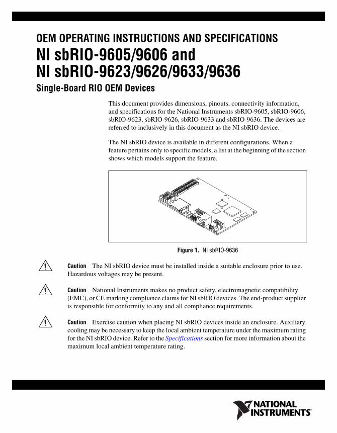
OEM OPERATING INSTRUCTIONS AND SPECIFICATIONS NI sbRIO-9605/9606 and NI sbRIO-9623/9626/9633/9636 Single-Board RIO OEM Devices This document provides dimensions, pinouts, connectivity information, and specifications for the National Instruments sbRIO-9605, sbRIO-9606, sbRIO-9623, sbRIO-9626, sbRIO-9633 and sbRIO-9636. The devices are referred to inclusively in this document as the NI sbRIO device. The NI sbRIO device is available in different configurations. When a feature pertains only to specific models, a list at the beginning of the section shows which models support the feature. Figure 1. NI sbRIO-9636 Caution The NI sbRIO device must be installed inside a suitable enclosure prior to use. Hazardous voltages may be present. Caution National Instruments makes no product safety, electromagnetic compatibility (EMC), or CE marking compliance claims for NI sbRIO devices. The end-product supplier is responsible for conformity to any and all compliance requirements. Caution Exercise caution when placing NI sbRIO devices inside an enclosure. Auxiliary cooling may be necessary to keep the local ambient temperature under the maximum rating for the NI sbRIO device. Refer to the Specifications section for more information about the maximum local ambient temperature rating.
Transcript of NI sbRIO-9605/9606/9623/9626/9633/9636 OEM … · OEM OPERATING INSTRUCTIONS AND SPECIFICATIONS NI...
OEM OPERATING INSTRUCTIONS AND SPECIFICATIONS
NI sbRIO-9605/9606 and NI sbRIO-9623/9626/9633/9636Single-Board RIO OEM Devices
This document provides dimensions, pinouts, connectivity information, and specifications for the National Instruments sbRIO-9605, sbRIO-9606, sbRIO-9623, sbRIO-9626, sbRIO-9633 and sbRIO-9636. The devices are referred to inclusively in this document as the NI sbRIO device.
The NI sbRIO device is available in different configurations. When a feature pertains only to specific models, a list at the beginning of the section shows which models support the feature.
Figure 1. NI sbRIO-9636
Caution The NI sbRIO device must be installed inside a suitable enclosure prior to use. Hazardous voltages may be present.
Caution National Instruments makes no product safety, electromagnetic compatibility (EMC), or CE marking compliance claims for NI sbRIO devices. The end-product supplier is responsible for conformity to any and all compliance requirements.
Caution Exercise caution when placing NI sbRIO devices inside an enclosure. Auxiliary cooling may be necessary to keep the local ambient temperature under the maximum rating for the NI sbRIO device. Refer to the Specifications section for more information about the maximum local ambient temperature rating.
NI sbRIO-960x/962x/963x OEM Instructions & Specifications 2 ni.com
Caution Do not operate the NI sbRIO device in a manner not specified in these operating instructions. Product misuse can result in a hazard. You can compromise the safety protection built into the product if the product is damaged in any way. If the product is damaged, return it to National Instruments for repair.
What You Need to Get StartedThis section lists the software and hardware you need to start programming the NI sbRIO device.
Software RequirementsYou need a development computer with the following software installed on it. Go to ni.com/info and enter the Info Code rdsoftwareversion for information about software version compatibility.
❑ LabVIEW 2011.1 or later
❑ LabVIEW Real-Time Module 2011.1 or later
❑ LabVIEW FPGA Module 2011.1 or later
❑ NI-RIO 4.1 or later
Hardware RequirementsYou need the following hardware to use the NI sbRIO device.
❑ NI sbRIO device
❑ 9–30 VDC power supply
❑ Power plug assembly
❑ Ethernet cable
© National Instruments 3 NI sbRIO-960x/962x/963x OEM Instructions & Specifications
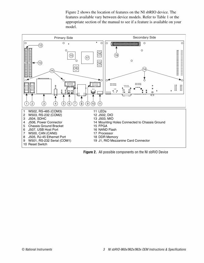
Figure 2 shows the location of features on the NI sbRIO device. The features available vary between device models. Refer to Table 1 or the appropriate section of the manual to see if a feature is available on your model.
Figure 2. All possible components on the NI sbRIO Device
1 W502, RS-485 (COM3)2 W503, RS-232 (COM2)3 J504, SDHC4 J506, Power Connector5 Chassis Ground Bracket6 J507, USB Host Port7 W500, CAN (CAN0)8 J505, RJ-45 Ethernet Port9 W501, RS-232 Serial (COM1)10 Reset Switch
11 LEDs12 J502, DIO13 J503, MIO14 Mounting Holes Connected to Chassis Ground15 FPGA16 NAND Flash17 Processor18 DDR Memory19 J1, RIO Mezzanine Card Connector
54 6 7 8 9 10 11
1416
1517
19
14
Primary Side Secondary Side
31 2
12
13
18
18
NI sbRIO-960x/962x/963x OEM Instructions & Specifications 4 ni.com
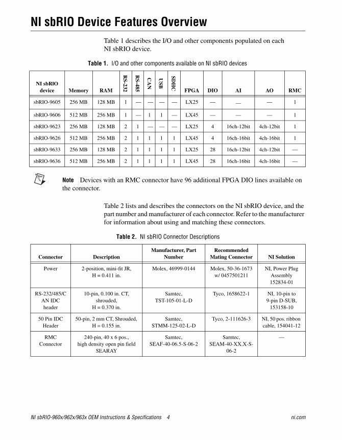
NI sbRIO Device Features OverviewTable 1 describes the I/O and other components populated on each NI sbRIO device.
Note Devices with an RMC connector have 96 additional FPGA DIO lines available on the connector.
Table 2 lists and describes the connectors on the NI sbRIO device, and the part number and manufacturer of each connector. Refer to the manufacturer for information about using and matching these connectors.
Table 1. I/O and other components available on NI sbRIO devices
NI sbRlO device Memory RAM
RS-232
RS-485
CA
N
USB
SDH
C
FPGA DIO AI AO RMC
sbRIO-9605 256 MB 128 MB 1 — — — — LX25 — — — 1
sbRIO-9606 512 MB 256 MB 1 — 1 1 — LX45 — — — 1
sbRIO-9623 256 MB 128 MB 2 1 — — — LX25 4 16ch-12bit 4ch-12bit 1
sbRIO-9626 512 MB 256 MB 2 1 1 1 1 LX45 4 16ch-16bit 4ch-16bit 1
sbRIO-9633 256 MB 128 MB 2 1 1 1 1 LX25 28 16ch-12bit 4ch-12bit —
sbRIO-9636 512 MB 256 MB 2 1 1 1 1 LX45 28 16ch-16bit 4ch-16bit —
Table 2. NI sbRIO Connector Descriptions
Connector DescriptionManufacturer, Part
NumberRecommended
Mating Connector NI Solution
Power 2-position, mini-fit JR, H = 0.411 in.
Molex, 46999-0144 Molex, 50-36-1673 w/ 0457501211
NI, Power Plug Assembly152834-01
RS-232/485/CAN IDC header
10-pin, 0.100 in. CT, shrouded,
H = 0.370 in.
Samtec, TST-105-01-L-D
Tyco, 1658622-1 NI, 10-pin to 9-pin D-SUB,
153158-10
50 Pin IDC Header
50-pin, 2 mm CT, Shrouded, H = 0.155 in.
Samtec, STMM-125-02-L-D
Tyco, 2-111626-3 NI, 50 pos. ribbon cable, 154041-12
RMC Connector
240-pin, 40 x 6 pos., high density open pin field
SEARAY
Samtec, SEAF-40-06.5-S-06-2
Samtec, SEAM-40-XX.X-S-
06-2
—
© National Instruments 5 NI sbRIO-960x/962x/963x OEM Instructions & Specifications
Note Samtec SEAM connectors come in multiple heights, indicated in mm by the XX.X portion of the following example part number: SEAM-40-XX.X-S-06-2. The height of the mating connector you select to mate to the RMC connector determines the height of the standoffs you need. Samtec, the connector manufacturer, requires that standoffs be 0.15 mm taller than the combined height of the RMC and mating connectors. Therefore, to determine the required standoff height, you must add the heights of the connectors plus 0.15 mm. For example, if you are using a SEAM-40-03.0-S-06-2 connector to mate to the RMC connector (SEAF-40-06.5-S-06-2), the required standoff height is 3.0 mm + 6.5 mm + 0.15 mm = 9.65 mm. Standoffs of this height are available from National Instruments (NI 153166-12) or Samtec (SO-0965-03-02-L-N). Consult Samtec for alternative heights and options. You must observe keepouts and maximum heights with all RMC and mating connector combinations.
NI sbRIO-960x/962x/963x OEM Instructions & Specifications 6 ni.com
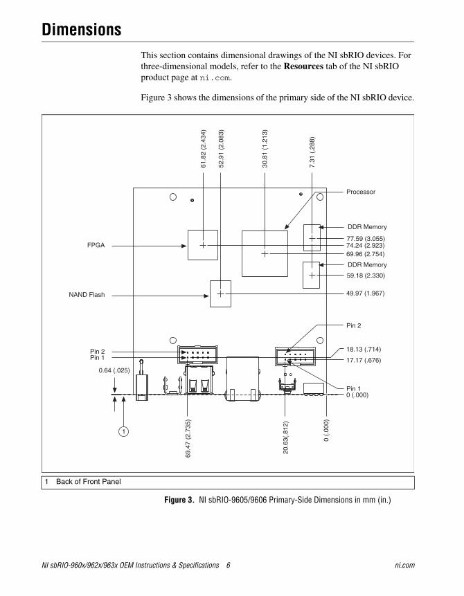
DimensionsThis section contains dimensional drawings of the NI sbRIO devices. For three-dimensional models, refer to the Resources tab of the NI sbRIO product page at ni.com.
Figure 3 shows the dimensions of the primary side of the NI sbRIO device.
Figure 3. NI sbRIO-9605/9606 Primary-Side Dimensions in mm (in.)
1 Back of Front Panel
0 (.000)
0.64 (.025)
0 (.
000)
FPGA
NAND Flash
Processor
20.6
3(.8
12)
Pin 1
17.17 (.676)
18.13 (.714)
Pin 2
49.97 (1.967)
69.96 (2.754)74.24 (2.923)
30.8
1 (1
.213
)
52.9
1 (2
.083
)
61.8
2 (2
.434
)
69.4
7 (2
.735
)
Pin 1Pin 2
77.59 (3.055)
7.31
(.2
88)
59.18 (2.330)
DDR Memory
DDR Memory
1
© National Instruments 7 NI sbRIO-960x/962x/963x OEM Instructions & Specifications
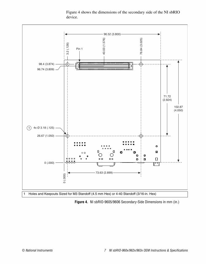
Figure 4 shows the dimensions of the secondary side of the NI sbRIO device.
Figure 4. NI sbRIO-9605/9606 Secondary-Side Dimensions in mm (in.)
1 Holes and Keepouts Sized for M3 Standoff (4.5 mm Hex) or 4-40 Standoff (3/16-in. Hex)
4x Ø 3.18 (.125)
0 (.
000)
26.67 (1.050)
3.2
(.12
6)
Pin 1
96.74 (3.809)
98.4 (3.874)
40.0
3 (1
.576
)
76.8
4 (3
.025
)
1
73.63 (2.899)
96.52 (3.800)
0 (.000)
71.72(2.824)
102.87(4.050)
NI sbRIO-960x/962x/963x OEM Instructions & Specifications 8 ni.com
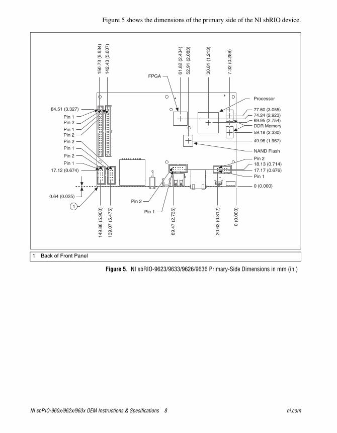
Figure 5 shows the dimensions of the primary side of the NI sbRIO device.
Figure 5. NI sbRIO-9623/9633/9626/9636 Primary-Side Dimensions in mm (in.)
1 Back of Front Panel
0 (0
.000
)
139.
07 (
5.47
5)
149.
86 (
5.90
0)
0 (0.000)
Pin 117.17 (0.676)18.13 (0.714)Pin 2
NAND Flash
49.96 (1.967)
59.18 (2.330)
DDR Memory69.95 (2.754)74.24 (2.923)77.60 (3.055)
Processor
84.51 (3.327)
17.12 (0.674)
0.64 (0.025)
Pin 1Pin 2Pin 2Pin 1
Pin 1
Pin 2
142.
43 (
5.60
7)
61. 8
2 (2
.434
)
FPGA
52.9
1 (2
.083
)
30.8
1 (1
.213
)
7.32
(0.
288)
20.6
3 (0
.812
)
69.4
7 (2
.735
)
Pin 2
Pin 1
150.
73 (
5.93
4)
Pin 1Pin 2
1
© National Instruments 9 NI sbRIO-960x/962x/963x OEM Instructions & Specifications
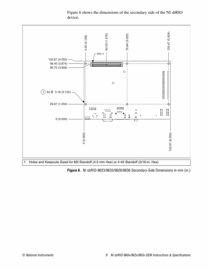
Figure 6 shows the dimensions of the secondary side of the NI sbRIO device.
Figure 6. NI sbRIO-9623/9633/9626/9636 Secondary-Side Dimensions in mm (in.)
1 Holes and Keepouts Sized for M3 Standoff (4.5 mm Hex) or 4-40 Standoff (3/16-in. Hex)
3.20
(0.
126)
40.0
3 (1
.576
)
76.8
4 (3
.025
)
150.
47 (
5.92
4)
Pin 1
0 (0.000)
26.67 (1.050)
3.18 (0.125)6x Ø
96.75 (3.809)98.40 (3.874)
102.87 (4.050)
0 (0
.000
)
153.
67 (
6.05
0)
1
NI sbRIO-960x/962x/963x OEM Instructions & Specifications 10 ni.com
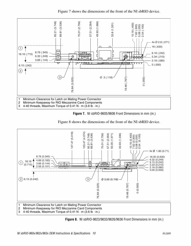
Figure 7 shows the dimensions of the front of the NI sbRIO device.
Figure 7. NI sbRIO-9605/9606 Front Dimensions in mm (in.)
Figure 8 shows the dimensions of the front of the NI sbRIO device.
Figure 8. NI sbRIO-9623/9633/9626/9636 Front Dimensions in mm (in.)
1 Minimum Clearance for Latch on Mating Power Connector2 Minimum Keepaway for RIO Mezzanine Card Components3 4-40 threads, Maximum Torque of 0.41 N · m (3.6 lb · in.)
1 Minimum Clearance for Latch on Mating Power Connector2 Minimum Keepaway for RIO Mezzanine Card Components3 4-40 threads, Maximum Torque of 0.41 N · m (3.6 lb · in.)
0 (.
000)Ø 3 (.118)
18.16 (.715)
16 (.630)
6.16 (.242)
0 (.000)
2.16 (.085)
5.34 (.210)
2.54
(.1
00)
5.08
(.2
00)
7.62
(.3
00)
10.1
6 (.
400)
33.8
(1.
331)
49.9
3 (1
.966
)
57.5
1 (2
.264
)
70.0
1 (2
.756
)
89.8
1 (3
.536
)
95.2
1 (3
.748
)8.76 (.345)
3.66 (.144)
6.32 (.249)
6.15 (.242)
19.4
8 (.
767)
76.8
4 (3
.025
)
4x Ø 2.8 (.071)
1
2
3
18.16(0.715)
6.15 (0.242)
2.56 (0.101)3.66 (0.144)4.66 (0.183)
8.76 (0.345)
5.33 (0.210)2.16 (0.085)
6.32 (0.249)6.15 (0.242)
16.00 (0.630)
Ø 3.00 (0.118)
0 (0
.000
)
19.4
8 (0
.767
)
76.8
4 (0
.025
)
127.
47 (
5.01
8)
103.
47 (
4.07
4)
95.2
1 (3
.748
)89
.81
(3.5
36)
70.0
1 (2
.756
)
57.5
1 (2
.264
)
50.0
5 (1
.971
)
33.9
3 (1
.336
)
10.1
6 (0
.400
)7.
62 (
0.30
0)5.
08 (
0.20
0)2.
54 (
0.10
0)
1.80 (0.71)4x Ø
0.00 (0.000)
3
1
2
© National Instruments 11 NI sbRIO-960x/962x/963x OEM Instructions & Specifications
Note For more information about the dimensions of the NI sbRIO device, including detailed dimensional drawings, go to ni.com/dimensions.
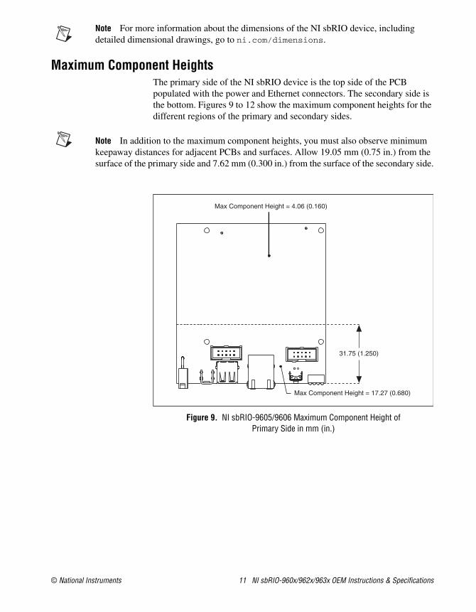
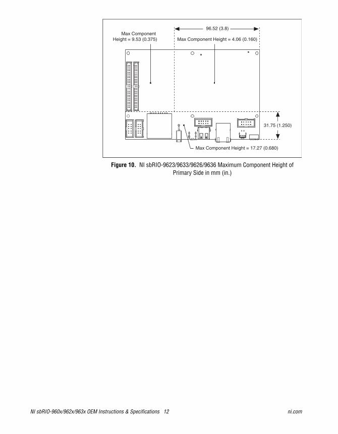
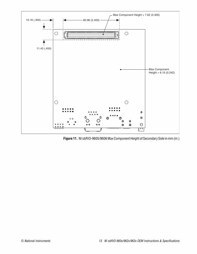
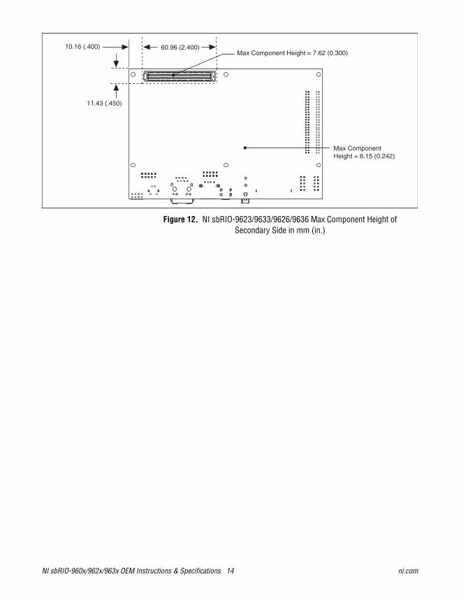
Maximum Component HeightsThe primary side of the NI sbRIO device is the top side of the PCB populated with the power and Ethernet connectors. The secondary side is the bottom. Figures 9 to 12 show the maximum component heights for the different regions of the primary and secondary sides.
Note In addition to the maximum component heights, you must also observe minimum keepaway distances for adjacent PCBs and surfaces. Allow 19.05 mm (0.75 in.) from the surface of the primary side and 7.62 mm (0.300 in.) from the surface of the secondary side.
Figure 9. NI sbRIO-9605/9606 Maximum Component Height of Primary Side in mm (in.)
Max Component Height = 4.06 (0.160)
Max Component Height = 17.27 (0.680)
31.75 (1.250)
NI sbRIO-960x/962x/963x OEM Instructions & Specifications 12 ni.com
Figure 10. NI sbRIO-9623/9633/9626/9636 Maximum Component Height of Primary Side in mm (in.)
Max Component Height = 4.06 (0.160)Max Component
Height = 9.53 (0.375)
Max Component Height = 17.27 (0.680)
31.75 (1.250)
96.52 (3.8)
© National Instruments 13 NI sbRIO-960x/962x/963x OEM Instructions & Specifications
Figure 11. NI sbRIO-9605/9606 Max Component Height of Secondary Side in mm (in.)
Max ComponentHeight = 6.15 (0.242)
Max Component Height = 7.62 (0.300)
60.96 (2.400)
11.43 (.450)
10.16 (.400)
NI sbRIO-960x/962x/963x OEM Instructions & Specifications 14 ni.com
Figure 12. NI sbRIO-9623/9633/9626/9636 Max Component Height of Secondary Side in mm (in.)
Max Component Height = 6.15 (0.242)
Max Component Height = 7.62 (0.300)60.96 (2.400)
11.43 (.450)
10.16 (.400)
© National Instruments 15 NI sbRIO-960x/962x/963x OEM Instructions & Specifications
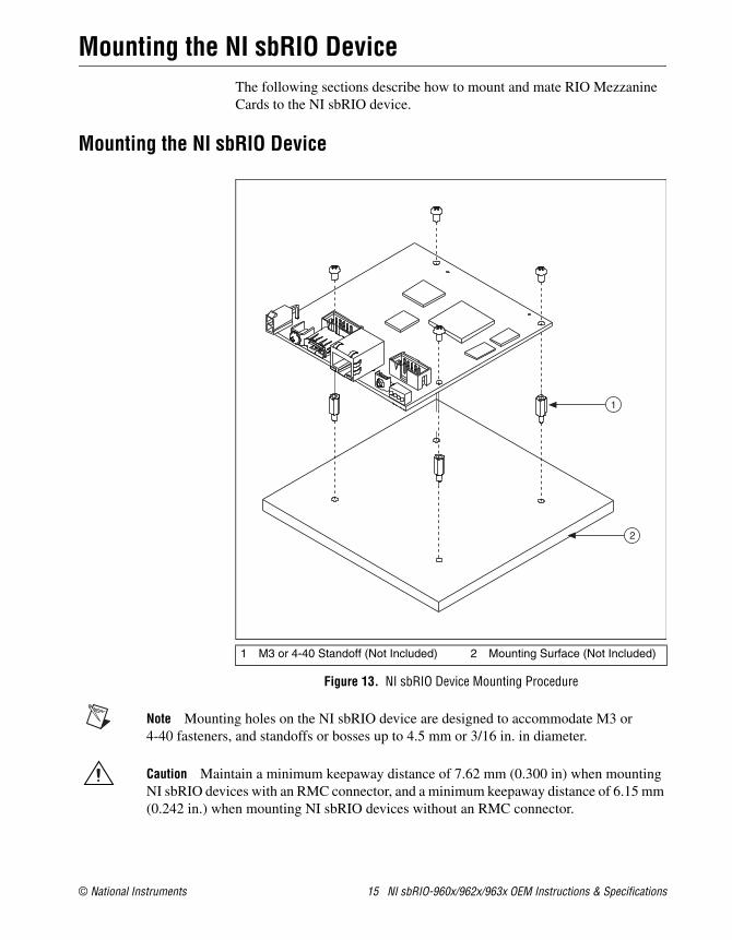
Mounting the NI sbRIO DeviceThe following sections describe how to mount and mate RIO Mezzanine Cards to the NI sbRIO device.
Mounting the NI sbRIO Device
Figure 13. NI sbRIO Device Mounting Procedure
Note Mounting holes on the NI sbRIO device are designed to accommodate M3 or 4-40 fasteners, and standoffs or bosses up to 4.5 mm or 3/16 in. in diameter.
Caution Maintain a minimum keepaway distance of 7.62 mm (0.300 in) when mounting NI sbRIO devices with an RMC connector, and a minimum keepaway distance of 6.15 mm (0.242 in.) when mounting NI sbRIO devices without an RMC connector.
1 M3 or 4-40 Standoff (Not Included) 2 Mounting Surface (Not Included)
1
2
NI sbRIO-960x/962x/963x OEM Instructions & Specifications 16 ni.com
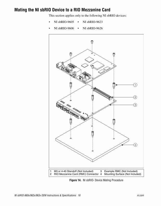
Mating the NI sbRIO Device to a RIO Mezzanine CardThis section applies only to the following NI sbRIO devices:
Figure 14. NI sbRIO- Device Mating Procedure
• NI sbRIO-9605 • NI sbRIO-9623
• NI sbRIO-9606 • NI sbRIO-9626
1 M3 or 4-40 Standoff (Not Included)2 RIO Mezzanine Card (RMC) Connector
3 Example RMC (Not Included)4 Mounting Surface (Not Included)
1
2
3
4
© National Instruments 17 NI sbRIO-960x/962x/963x OEM Instructions & Specifications
Understanding Ground ConnectionsThe front I/O connector shields, chassis ground bracket, and mounting holes near the front I/O are connected together internally to form chassis ground. Chassis ground is capacitively coupled to digital ground near the power connector. For the best possible ESD protection, connect chassis ground at the mounting holes or the chassis ground bracket to a low inductance earth ground.
When connecting the NI sbRIO device to external devices, ensure that stray ground currents are not using the device as a return path. Significant stray currents traversing through the NI sbRIO device can result in device failure.
To verify correct grounding of the NI sbRIO device, make sure the current flowing into the power connector equals the current flowing out of the power connector. These currents should be measured with a current probe after final assembly of the end system. Investigate and remove any current differences.
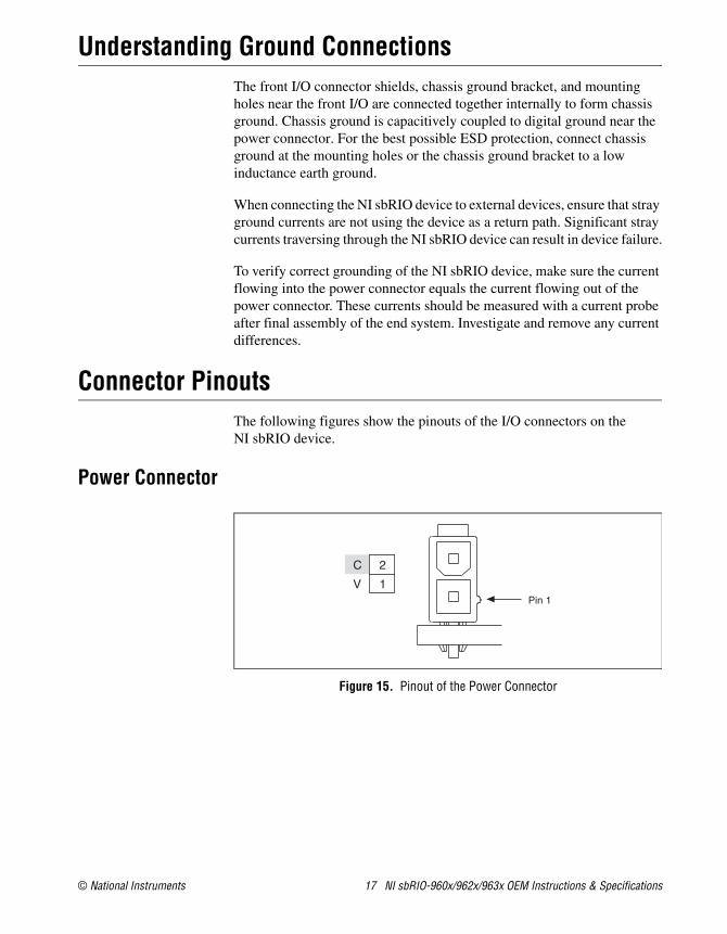
Connector PinoutsThe following figures show the pinouts of the I/O connectors on the NI sbRIO device.
Power Connector
Figure 15. Pinout of the Power Connector
V
C 2
1Pin 1
NI sbRIO-960x/962x/963x OEM Instructions & Specifications 18 ni.com
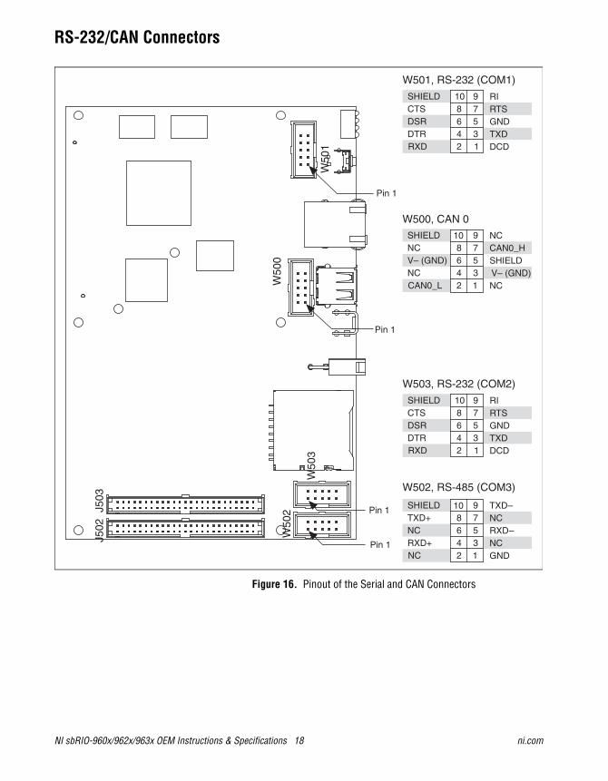
RS-232/CAN Connectors
Figure 16. Pinout of the Serial and CAN Connectors
CAN0_LNCV– (GND)NCSHIELD
NC
SHIELDCAN0_H
V– (GND)
NC10 98 76 54 32 1
Pin 1
RXDDTRDSRCTSSHIELD
DCD
GNDRTS
TXD
RI10 98 7
564 32 1
Pin 1
NCRXD+NCTXD+SHIELD
GND
RXD–NC
NC
TXD–10 98 76 54 32 1
RXDDTRDSRCTSSHIELD
DCD
GNDRTS
TXD
RI10 98 7
564 32 1
W500, CAN 0
W501, RS-232 (COM1)
W502, RS-485 (COM3)
W503, RS-232 (COM2)
Pin 1
Pin 1
J503
J502
W50
2
W50
3
W50
0
W50
1
© National Instruments 19 NI sbRIO-960x/962x/963x OEM Instructions & Specifications
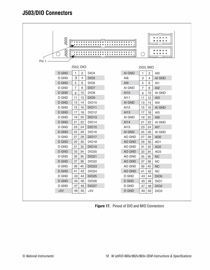
J503/DIO Connectors
Figure 17. Pinout of DIO and MIO Connectors
D GND
D GND
D GND
D GND
AO GND
AO GND
AO GND
AO GND
AO GND
AO GND
AO GND
AO GND
AI GND
AI15
AI14
AI GND
AI13
AI12
AI GND
AI11
AI10
AI GND
AI9
AI8
AI GND
+5V
D GND
D GND
D GND
D GND
D GND
D GND
D GND
D GND
D GND
D GND
D GND
D GND
D GND
D GND
D GND
D GND
D GND
D GND
D GND
D GND
D GND
D GND
D GND
D GND
+5V
DIO26
DIO25
DIO23
DIO22
DIO21
DIO20
DIO27
DIO24
DIO19
DIO18
DIO17
DIO16
DIO15
DIO14
DIO13
DIO12
DIO11
DIO10
DIO9
DIO8
DIO7
DIO6
DIO5
DIO4 1 2
3 4
5 6
7 8
9 10
11 12
13 14
15 16
17 18
19 20
21 22
23 24
25 26
27 28
29 30
31 32
33 34
35 36
37 38
39 40
41 42
43 44
45 46
47 48
49 50 DIO3
DIO1
DIO0
NC
NC
NC
AO3
DIO2
NC
AO2
AO1
AO0
AI GND
AI7
AI GND
AI6
AI5
AI GND
AI4
AI3
AI GND
AI2
AI1
AI GND
AI0 1 2
3 4
5 6
7 8
9 10
11 12
13 14
15 16
17 18
19 20
21 22
23 24
25 26
27 28
29 30
31 32
33 34
35 36
37 38
39 40
41 42
43 44
45 46
47 48
49 50
Pin 1
J502, DIO J503, MIOJ5
03J5
02
NI sbRIO-960x/962x/963x OEM Instructions & Specifications 20 ni.com
RIO Mezzanine Card ConnectorThis section applies only to the following NI sbRIO devices:
The RIO Mezzanine Card connector provides connections for 96 FPGA I/O channels, as well as pins reserved for future use.
The table on the following page lists the pinout for the RIO Mezzanine Card connector, indicating the pin number and corresponding function.
Note Users interested in additional processor functionality such as serial, CAN, USB, or Ethernet should contact a local National Instruments representative for custom design opportunities. A non-recurring engineering charge (NRE) may apply.
Note Reserved and unused lines should be left disconnected on RIO Mezzanine Cards. Future versions of this manual may update their definition.
Note National Instruments suggests using pins DIO0 through DIO63 first to maintain future compatibility. DIO64 through DIO95 are not guaranteed to be provided on future products.
Caution RMCs are not hot-swappable. Disconnect power before mating or unmating.
• NI sbRIO-9605 • NI sbRIO-9623
• NI sbRIO-9605 • NI sbRIO-9626
© National Instruments 21 NI sbRIO-960x/962x/963x OEM Instructions & Specifications
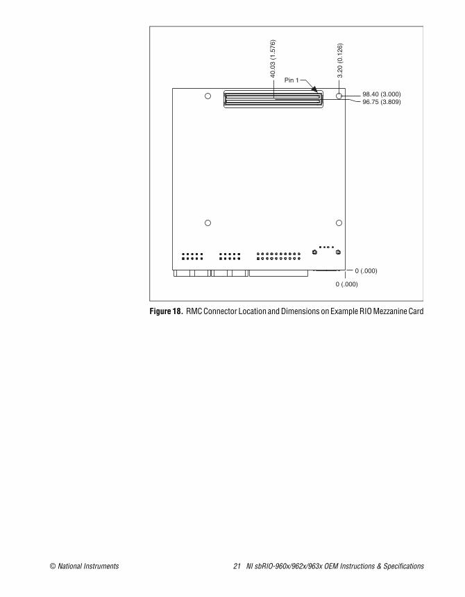
Figure 18. RMC Connector Location and Dimensions on Example RIO Mezzanine Card
98.40 (3.000)96.75 (3.809)
3.20
(0.
126)
40.0
3 (1
.576
)
Pin 1
0 (.000)
0 (.000)
NI sbRIO-960x/962x/963x OEM Instructions & Specifications 22 ni.com
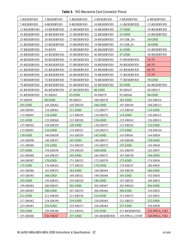
Table 3. RIO Mezzanine Card Connector Pinout
1-RESERVED 2-RESERVED 3-RESERVED 4-RESERVED 5-RESERVED 6-RESERVED
7-RESERVED 8-RESERVED 9-RESERVED 10-RESERVED 11-RESERVED 12-RESERVED
13-RESERVED 14-RESERVED 15-RESERVED 16-RESERVED 17-GND 18-RESERVED
19-RESERVED 20-RESERVED 21-RESERVED 22-RESERVED 23-GND 24-RESERVED
25-RESERVED 26-RESERVED 27-RESERVED 28-RESERVED 29-USB_D+ 30-GND
31-RESERVED 32-RESERVED 33-RESERVED 34-RESERVED 35-USB_D– 36-GND
37-RESERVED 38-RST# 39-RESERVED 40-RESERVED 41-GND 42-RESERVED
43-RESERVED 44-RESERVED 45-RESERVED 46-RESERVED 47-GND 48-RESERVED
49-RESERVED 50-RESERVED 51-RESERVED 52-RESERVED 53-RESERVED 54-5V
55-RESERVED 56-RESERVED 57-RESERVED 58-RESERVED 59-RESERVED 60-5V
61-RESERVED 62-RESERVED 63-RESERVED 64-RESERVED 65-RESERVED 66-5V
67-RESERVED 68-RESERVED 69-RESERVED 70-RESERVED 71-RESERVED 72-5V
73-RESERVED 74-RESERVED 75-RESERVED 76-RESERVED 77-RESERVED 78-GND
79-RESERVED 80-RESERVED 81-RESERVED 82-RESERVED 83-GND 84-RESERVED
85-RESERVED 86-RESERVED 87-RESERVED 88-GND 89-DIO47 90-DIO15
91-RESERVED 92-DIO63 93-GND 94-DIO79 95-DIO46 96-GND
97-DIO95 98-GND 99-DIO31 100-DIO78 101-GND 102-DIO14
103-GND 104-DIO62 105-DIO30 106-GND 107-DIO45 108-DIO13
109-DIO94 110-DIO61 111-GND 112-DIO77 113-DIO44 114-GND
115-DIO93 116-GND 117-DIO29 118-DIO76 119-GND 120-DIO12
121-GND 122-DIO60 123-DIO28 124-GND 125-DIO43 126-DIO11
127-DIO92 128-DIO59 129-GND 130-DIO75 131-DIO42 132-GND
133-DIO91 134-GND 135-DIO27 136-DIO74 137-GND 138-DIO10
139-GND 140-DIO58 141-DIO26 142-GND 143-DIO41 144-DIO9
145-DIO90 146-DIO57 147-GND 148-DIO73 149-DIO40 150-GND
151-DIO89 152-GND 153-DIO25 154-DIO72 155-GND 156-DIO8
157-GND 158-DIO56 159-DIO24 160-GND 161-DIO39 162-DIO7
163-DIO88 164-DIO55 165-GND 166-DIO71 167-DIO38 168-GND
169-DIO87 170-GND 171-DIO23 172-DIO70 173-GND 174-DIO6
175-GND 176-DIO54 177-DIO22 178-GND 179-DIO37 180-DIO5
181-DIO86 182-DIO53 183-GND 184-DIO69 185-DIO36 186-GND
187-DIO85 188-GND 189-DIO21 190-DIO68 191-GND 192-DIO4
193-GND 194-DIO52 195-DIO20 196-GND 197-DIO35 198-DIO3
199-DIO84 200-DIO51 201-GND 202-DIO67 203-DIO34 204-GND
205-DIO83 206-GND 207-DIO19 208-DIO66 209-GND 210-DIO2
211-GND 212-DIO50 213-DIO18 214-GND 215-DIO33 216-DIO1
217-DIO82 218-DIO49 219-GND 220-DIO65 221-DIO32 222-GND
223-DIO81 224-GND 225-DIO17 226-DIO64 227-GND 228-DIO0
229-GND 230-DIO48 231-DIO16 232-GND 233-RESERVED 234-FPGA_VIO
235-DIO80 236-VBAT 237-GND 238-RESERVED 239-FPGA_CONF 240-FPGA_VIO
© National Instruments 23 NI sbRIO-960x/962x/963x OEM Instructions & Specifications
RMC Power RequirementsThe RIO Mezzanine Card connector provides power on six pins. The 5 V rail consists of pins 54, 60, 66, and 72, and is the main source of power to a RIO Mezzanine Card. The FPGA_VIO rail consists of pins 234 and 240, and is used to supply I/O power and determine I/O levels for the FPGA I/O pins.
Table 4 lists the rail requirements for each of the rails on a RIO Mezzanine Card connector.
RIO Mezzanine Cards should not source any current onto any of the power pins and should be able to tolerate 5 V and FPGA_VIO coming up in any order.
RMC VBATThe NI sbRIO device implements an onboard real-time clock (RTC) to keep track of absolute time. The RMC connector provides a VBAT line to power the RTC. Without a battery, absolute time will be reset during a power cycle. Batteries connected to VBAT must have a nominal output between 3.0 V and 3.6 V, and a maximum output of 3.7 V. If VBAT is not being used, leave it disconnected.
USB on RMC ConnectorThe USB pair on the RMC Connector has a 90 Ω differential trace impedance. To ensure the best possible signal integrity, route the USB pair with a similar trace impedance. If USB is not being used, leave it disconnected.
RMC RST#The RST# signal indicates that power provided through the RMC Connector is valid. RST# is guaranteed to be asserted (active low) for at least 1 ms when the controller is powered up or reset. There should be no more than 30 pF on the RST# line of a RIO Mezzanine Card. This includes the RMC Connector, traces, vias, and device pins. Refer to 3.3 V Digital I/O on RIO Mezzanine Card Connector in the Specifications section for output logic levels.
Table 4. NI RIO Mezzanine Card Rail Requirements
Voltage Tolerance Max Current Max Ripple and Noise
5 V +/– 5% 1.5 A 50 mV
FPGA_VIO (3.3 V) +/– 5% 0.33 A 50 mV
NI sbRIO-960x/962x/963x OEM Instructions & Specifications 24 ni.com
FPGA_CONFThe FPGA_CONF signal asserts high when the FPGA has been programmed. When the FPGA is unconfigured the signal is floating. A pulldown resistor is required when using this signal to ensure it returns to ground.
3.3 V Digital I/OThe NI sbRIO device provides 3.3 V digital I/O via the RIO Mezzanine Card connector and the 50-pin IDC headers. The following sections provide figures and specifications for a single DIO channel on each connector.
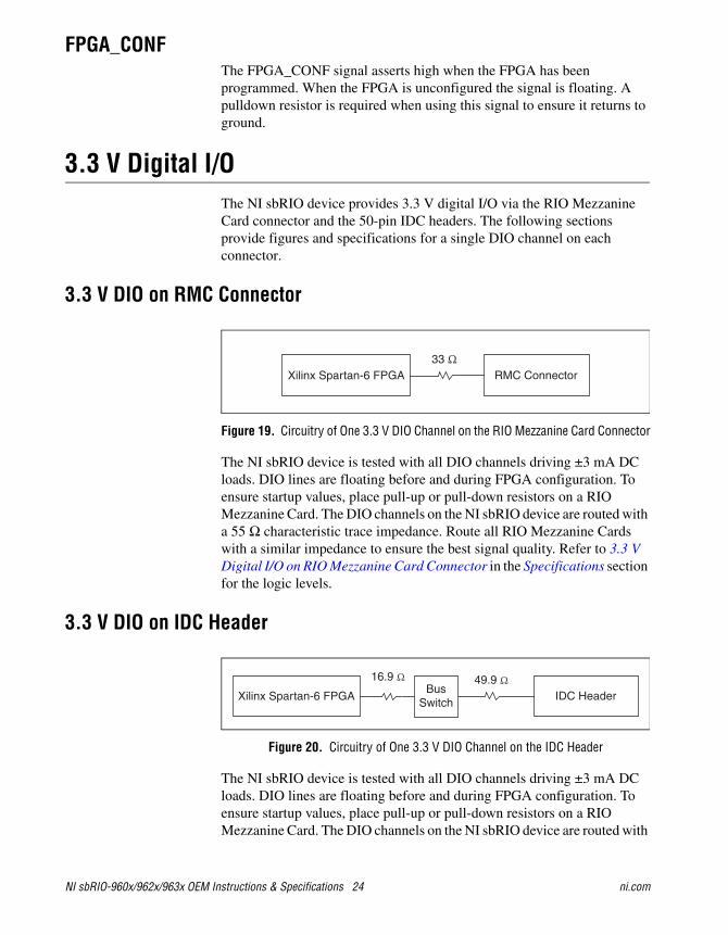
3.3 V DIO on RMC Connector
Figure 19. Circuitry of One 3.3 V DIO Channel on the RIO Mezzanine Card Connector
The NI sbRIO device is tested with all DIO channels driving ±3 mA DC loads. DIO lines are floating before and during FPGA configuration. To ensure startup values, place pull-up or pull-down resistors on a RIO Mezzanine Card. The DIO channels on the NI sbRIO device are routed with a 55 Ω characteristic trace impedance. Route all RIO Mezzanine Cards with a similar impedance to ensure the best signal quality. Refer to 3.3 V Digital I/O on RIO Mezzanine Card Connector in the Specifications section for the logic levels.
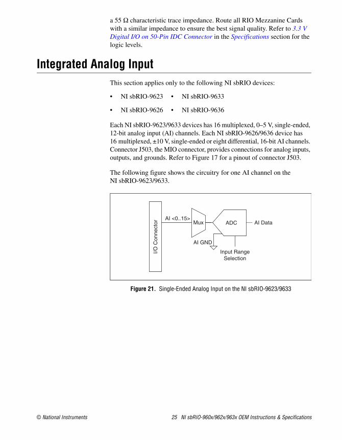
3.3 V DIO on IDC Header
Figure 20. Circuitry of One 3.3 V DIO Channel on the IDC Header
The NI sbRIO device is tested with all DIO channels driving ±3 mA DC loads. DIO lines are floating before and during FPGA configuration. To ensure startup values, place pull-up or pull-down resistors on a RIO Mezzanine Card. The DIO channels on the NI sbRIO device are routed with
Xilinx Spartan-6 FPGA RMC Connector33 Ω
Xilinx Spartan-6 FPGA IDC Header49.9 Ω
BusSwitch
16.9 Ω
© National Instruments 25 NI sbRIO-960x/962x/963x OEM Instructions & Specifications
a 55 Ω characteristic trace impedance. Route all RIO Mezzanine Cards with a similar impedance to ensure the best signal quality. Refer to 3.3 V Digital I/O on 50-Pin IDC Connector in the Specifications section for the logic levels.
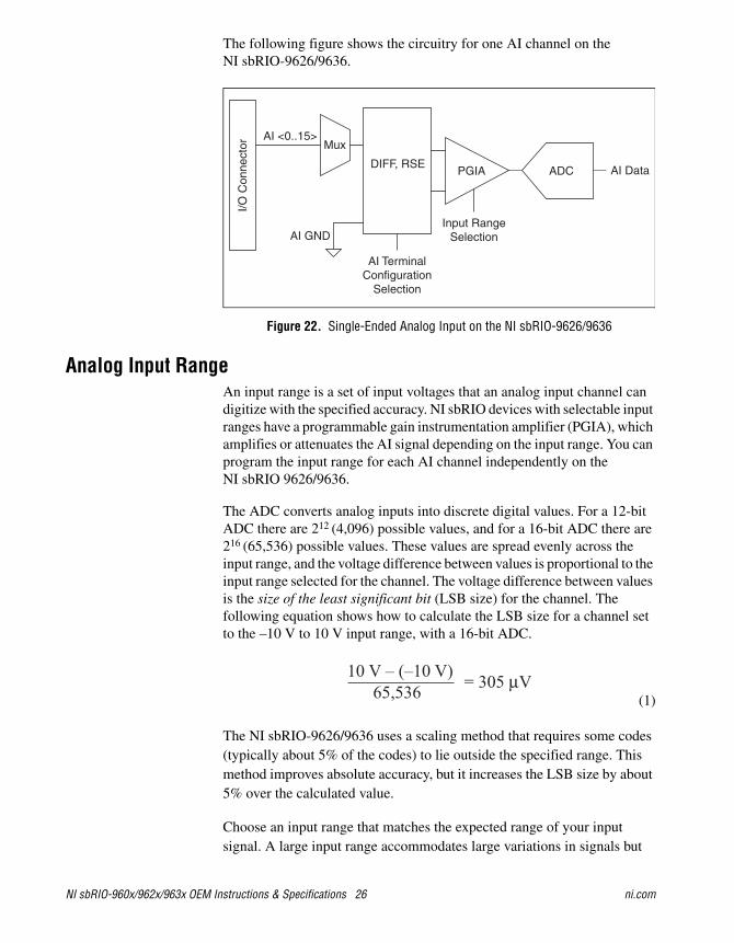
Integrated Analog InputThis section applies only to the following NI sbRIO devices:
Each NI sbRIO-9623/9633 devices has 16 multiplexed, 0–5 V, single-ended, 12-bit analog input (AI) channels. Each NI sbRIO-9626/9636 device has 16 multiplexed, ±10 V, single-ended or eight differential, 16-bit AI channels. Connector J503, the MIO connector, provides connections for analog inputs, outputs, and grounds. Refer to Figure 17 for a pinout of connector J503.
The following figure shows the circuitry for one AI channel on the NI sbRIO-9623/9633.
Figure 21. Single-Ended Analog Input on the NI sbRIO-9623/9633
• NI sbRIO-9623 • NI sbRIO-9633
• NI sbRIO-9626 • NI sbRIO-9636
I/O C
onne
ctor
AI <0..15>Mux
AI GND
Input RangeSelection
ADC AI Data
NI sbRIO-960x/962x/963x OEM Instructions & Specifications 26 ni.com
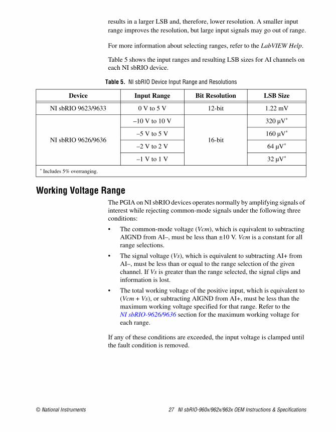
The following figure shows the circuitry for one AI channel on the NI sbRIO-9626/9636.
Figure 22. Single-Ended Analog Input on the NI sbRIO-9626/9636
Analog Input RangeAn input range is a set of input voltages that an analog input channel can digitize with the specified accuracy. NI sbRIO devices with selectable input ranges have a programmable gain instrumentation amplifier (PGIA), which amplifies or attenuates the AI signal depending on the input range. You can program the input range for each AI channel independently on the NI sbRIO 9626/9636.
The ADC converts analog inputs into discrete digital values. For a 12-bit ADC there are 212 (4,096) possible values, and for a 16-bit ADC there are 216 (65,536) possible values. These values are spread evenly across the input range, and the voltage difference between values is proportional to the input range selected for the channel. The voltage difference between values is the size of the least significant bit (LSB size) for the channel. The following equation shows how to calculate the LSB size for a channel set to the –10 V to 10 V input range, with a 16-bit ADC.
(1)
The NI sbRIO-9626/9636 uses a scaling method that requires some codes (typically about 5% of the codes) to lie outside the specified range. This method improves absolute accuracy, but it increases the LSB size by about 5% over the calculated value.
Choose an input range that matches the expected range of your input signal. A large input range accommodates large variations in signals but
DIFF, RSE
I/O C
onne
ctor
AI <0..15>Mux
AI GND
PGIA
AI TerminalConfiguration
Selection
Input RangeSelection
ADC AI Data
10 V – (–10 V)65,536 = 305 μV
© National Instruments 27 NI sbRIO-960x/962x/963x OEM Instructions & Specifications
results in a larger LSB and, therefore, lower resolution. A smaller input range improves the resolution, but large input signals may go out of range.
For more information about selecting ranges, refer to the LabVIEW Help.
Table 5 shows the input ranges and resulting LSB sizes for AI channels on each NI sbRIO device.
Working Voltage RangeThe PGIA on NI sbRIO devices operates normally by amplifying signals of interest while rejecting common-mode signals under the following three conditions:
• The common-mode voltage (Vcm), which is equivalent to subtracting AIGND from AI–, must be less than ±10 V. Vcm is a constant for all range selections.
• The signal voltage (Vs), which is equivalent to subtracting AI+ from AI–, must be less than or equal to the range selection of the given channel. If Vs is greater than the range selected, the signal clips and information is lost.
• The total working voltage of the positive input, which is equivalent to (Vcm + Vs), or subtracting AIGND from AI+, must be less than the maximum working voltage specified for that range. Refer to the NI sbRIO-9626/9636 section for the maximum working voltage for each range.
If any of these conditions are exceeded, the input voltage is clamped until the fault condition is removed.
Table 5. NI sbRIO Device Input Range and Resolutions
Device Input Range Bit Resolution LSB Size
NI sbRIO 9623/9633 0 V to 5 V 12-bit 1.22 mV
NI sbRIO 9626/9636
–10 V to 10 V
16-bit
320 µV*
–5 V to 5 V 160 µV*
–2 V to 2 V 64 µV*
–1 V to 1 V 32 µV*
* Includes 5% overranging.
NI sbRIO-960x/962x/963x OEM Instructions & Specifications 28 ni.com
Best Practices for Scanning Multiple ChannelsNI sbRIO devices can scan multiple channels at high rates and digitize the signals accurately. If your application scans multiple channels, settling error can affect the accuracy of your measurements. Settling error is a difference between the input value and the value that the ADC digitizes, and is the result of switching between multiplexed input channels. National Instruments defines settling error as the difference between a single-channel measurement of a signal and a multiple-channel measurement of the same signal. Settling errors are directly proportional to channel-to-channel voltage step size and the time between acquisitions. NI sbRIO devices scan at a fixed rate equal to the maximum aggregate rate.
To ensure the lowest possible settling errors, design your application according to the following best practices:
1. Use Low-Impedance Sources—Ensure that the impedance of signal sources is less than 1 kΩ. High-impedance sources increase settling errors and decrease accuracy at fast scanning rates. You can reduce impedance by connecting a voltage-follower circuit between the signal source and the AI pin of the channel. For more information about reducing impedance, go to ni.com/info and entering the Info Code rdbbis.
2. Use Short, High-Quality Cabling—Using short, high-quality cables can minimize several effects that degrade accuracy, including crosstalk, transmission line effects, and noise. The capacitance of the cable can also increase the settling error. National Instruments recommends using individually shielded twisted-pair wires shorter than 2 m to connect AI signals to the device. Refer to the Connecting Analog Input Signals section for more information.
3. Minimize Voltage Step between Adjacent Channels—Settling error increases with the voltage step between channels. If you know the expected input ranges of your signals, you can group signals with similar expected ranges together on adjacent channels.
Note When you program your I/O node with a scan list, the NI sbRIO device scans channels in numerical order at a fixed rate. Calling a second I/O node adds an extra delay before the first channel but does not reduce settling error.
© National Instruments 29 NI sbRIO-960x/962x/963x OEM Instructions & Specifications
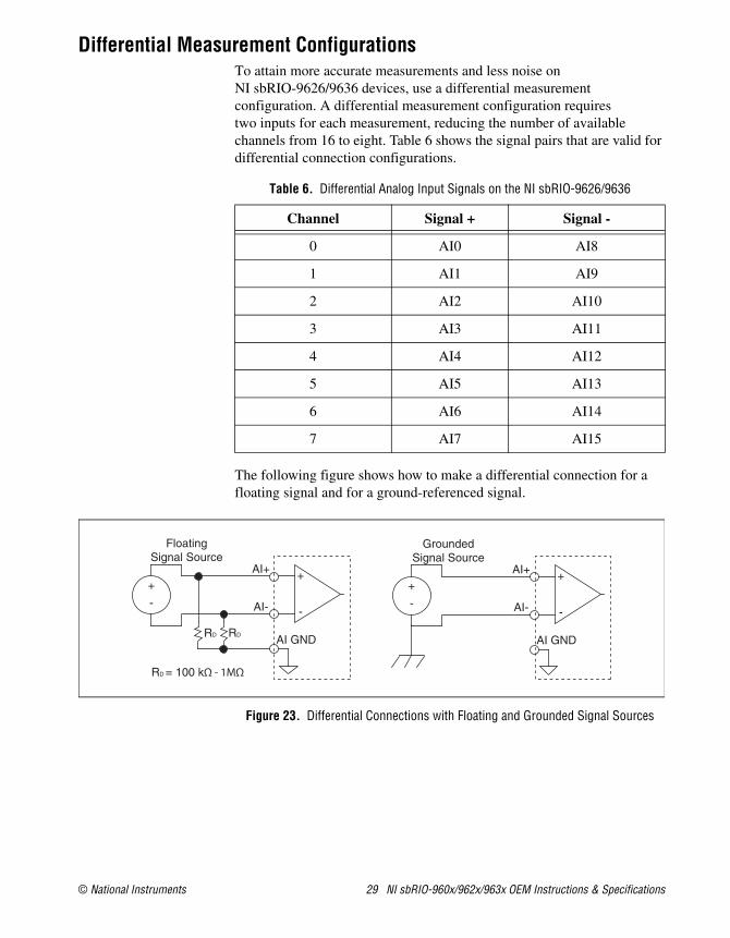
Differential Measurement ConfigurationsTo attain more accurate measurements and less noise on NI sbRIO-9626/9636 devices, use a differential measurement configuration. A differential measurement configuration requires two inputs for each measurement, reducing the number of available channels from 16 to eight. Table 6 shows the signal pairs that are valid for differential connection configurations.
The following figure shows how to make a differential connection for a floating signal and for a ground-referenced signal.
Figure 23. Differential Connections with Floating and Grounded Signal Sources
Table 6. Differential Analog Input Signals on the NI sbRIO-9626/9636
Channel Signal + Signal -
0 AI0 AI8
1 AI1 AI9
2 AI2 AI10
3 AI3 AI11
4 AI4 AI12
5 AI5 AI13
6 AI6 AI14
7 AI7 AI15
+
-
RD RD
+
-
RD = 100 kΩ - 1MΩ
AI+
AI-
AI GND
FloatingSignal Source
+
-
+
-
AI+
AI-
AI GND
GroundedSignal Source
NI sbRIO-960x/962x/963x OEM Instructions & Specifications 30 ni.com
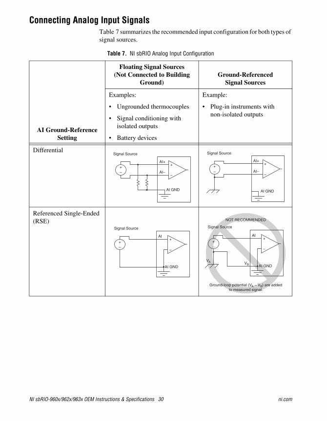
Connecting Analog Input SignalsTable 7 summarizes the recommended input configuration for both types of signal sources.
Table 7. NI sbRIO Analog Input Configuration
AI Ground-Reference Setting
Floating Signal Sources (Not Connected to Building
Ground)Ground-Referenced
Signal Sources
Examples:
• Ungrounded thermocouples
• Signal conditioning with isolated outputs
• Battery devices
Example:
• Plug-in instruments with non-isolated outputs
Differential
Referenced Single-Ended (RSE)
+–
+
–
AI+
AI–
AI GND
Signal Source
+–
+
–
AI+
AI–
AI GND
Signal Source
+–
+
–
AI
AI GND
Signal Source
Ground-loop potential (VA – VB) are addedto measured signal.
NOT RECOMMENDED
+–
+
–
AI
AI GNDVB
VA
Signal Source
© National Instruments 31 NI sbRIO-960x/962x/963x OEM Instructions & Specifications
Connecting Floating Signal Sources
What Are Floating Signal Sources?A floating signal source is not connected to the building ground system, but has an isolated ground-reference point. Some examples of floating signal sources are outputs of transformers, thermocouples, battery-powered devices, optical isolators, and isolation amplifiers. An instrument or device that has an isolated output is a floating signal source.
When to Use Differential Connections with Floating Signal SourcesUse DIFF input connections for any channel that meets any of the following conditions:
• The input signal is low level (less than 1 V).
• The leads connecting the signal to the device are greater than 3 m (10 ft).
• The input signal requires a separate ground-reference point or return signal.
• The signal leads travel through noisy environments.
• Two analog input channels, AI+ and AI–, are available for the signal.
DIFF signal connections reduce noise pickup and increase common-mode noise rejection. DIFF signal connections also allow input signals to float within the common-mode limits of the PGIA.
Refer to the Using Differential Connections for Floating Signal Sources section for more information about differential connections.
When to Use Referenced Single-Ended (RSE) Connections with Floating Signal SourcesOnly use RSE input connections if the input signal meets the following conditions:
• The input signal can share a common reference point, AI GND, with other signals that use RSE.
• The input signal is high-level (greater than 1 V).
• The leads connecting the signal to the device are less than 3 m (10 ft).
DIFF input connections are recommended for greater signal integrity for any input signal that does not meet the preceding conditions.
In the single-ended modes, more electrostatic and magnetic noise couples into the signal connections than in DIFF configurations. The coupling is the
NI sbRIO-960x/962x/963x OEM Instructions & Specifications 32 ni.com
result of differences in the signal path. Magnetic coupling is proportional to the area between the two signal conductors. Electrical coupling is a function of how much the electric field differs between the two conductors.
With this type of connection, the NI sbRIO device rejects both the common-mode noise in the signal and the ground potential difference between the signal source and the device ground.
Using Differential Connections for Floating Signal SourcesIt is important to connect the negative lead of a floating source to AI GND (either directly or through a bias resistor). Otherwise, the source may float out of the maximum working voltage range of the PGIA device and the return erroneous data.
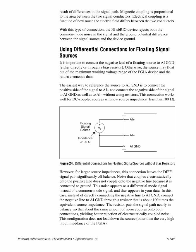
The easiest way to reference the source to AI GND is to connect the positive side of the signal to AI+ and connect the negative side of the signal to AI GND as well as to AI– without using resistors. This connection works well for DC-coupled sources with low source impedance (less than 100 Ω).
Figure 24. Differential Connections for Floating Signal Sources without Bias Resistors
However, for larger source impedances, this connection leaves the DIFF signal path significantly off balance. Noise that couples electrostatically onto the positive line does not couple onto the negative line because it is connected to ground. This noise appears as a differential mode signal instead of a common-mode signal, and thus appears in your data. In this case, instead of directly connecting the negative line to AI GND, connect the negative line to AI GND through a resistor that is about 100 times the equivalent source impedance. The resistor puts the signal path nearly in balance, so that about the same amount of noise couples onto both connections, yielding better rejection of electrostatically coupled noise. This configuration does not load down the source (other than the very high input impedance of the PGIA).
–
+
Inpedance<100 Ω
AI GND
AI+
AI–
Vs
FloatingSignalSource
© National Instruments 33 NI sbRIO-960x/962x/963x OEM Instructions & Specifications
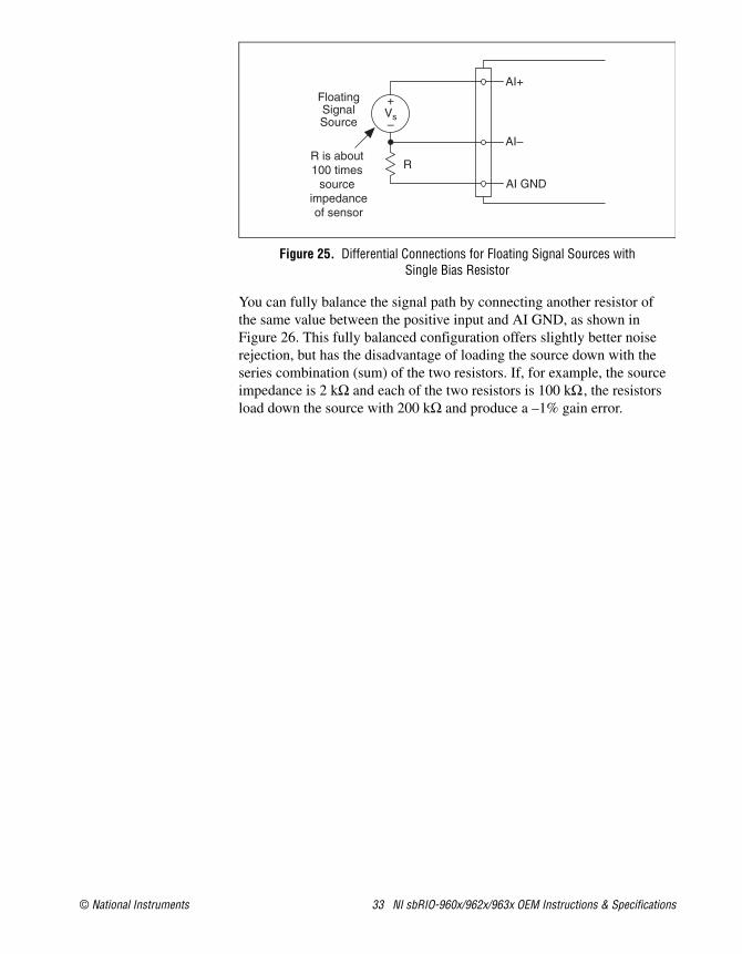
Figure 25. Differential Connections for Floating Signal Sources with Single Bias Resistor
You can fully balance the signal path by connecting another resistor of the same value between the positive input and AI GND, as shown in Figure 26. This fully balanced configuration offers slightly better noise rejection, but has the disadvantage of loading the source down with the series combination (sum) of the two resistors. If, for example, the source impedance is 2 kΩ and each of the two resistors is 100 kΩ , the resistors load down the source with 200 kΩ and produce a –1% gain error.
–
+
R is about 100 times
source impedanceof sensor
AI GND
R
Vs
FloatingSignalSource
AI+
AI–
NI sbRIO-960x/962x/963x OEM Instructions & Specifications 34 ni.com
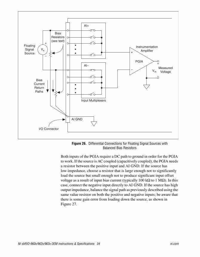
Figure 26. Differential Connections for Floating Signal Sources with Balanced Bias Resistors
Both inputs of the PGIA require a DC path to ground in order for the PGIA to work. If the source is AC coupled (capacitively coupled), the PGIA needs a resistor between the positive input and AI GND. If the source has low-impedance, choose a resistor that is large enough not to significantly load the source but small enough not to produce significant input offset voltage as a result of input bias current (typically 100 kΩ to 1 MΩ). In this case, connect the negative input directly to AI GND. If the source has high output impedance, balance the signal path as previously described using the same value resistor on both the positive and negative inputs; be aware that there is some gain error from loading down the source, as shown in Figure 27.
PGIA
–
+
–
+
–
+
FloatingSignalSource
BiasCurrentReturnPaths
AI GND
Input Multiplexers
MeasuredVoltage
InstrumentationAmplifier
AI+
AI–
I/O Connector
BiasResistors(see text)
Vs
Vm
© National Instruments 35 NI sbRIO-960x/962x/963x OEM Instructions & Specifications
Figure 27. Differential Connections for AC Coupled Floating Sources with Balanced Bias Resistors
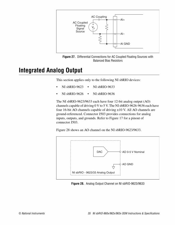
Integrated Analog OutputThis section applies only to the following NI sbRIO devices:
The NI sbRIO-9623/9633 each have four 12-bit analog output (AO) channels capable of driving 0 V to 5 V. The NI sbRIO-9626-9636 each have four 16-bit AO channels capable of driving ±10 V. All AO channels are ground-referenced. Connector J503 provides connections for analog inputs, outputs, and grounds. Refer to Figure 17 for a pinout of connector J503.
Figure 28 shows an AO channel on the NI sbRIO-9623/9633.
Figure 28. Analog Output Channel on NI sbRIO-9623/9633
• NI sbRIO-9623 • NI sbRIO-9633
• NI sbRIO-9626 • NI sbRIO-9636
–
+
AI GND
Vs
AC CoupledFloatingSignalSource
AI+
AI–
AC Coupling
DAC
NI sbRIO - 9623/33 Analog Output
AO 0-5 V Nominal
AO GND
NI sbRIO-960x/962x/963x OEM Instructions & Specifications 36 ni.com
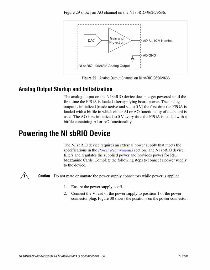
Figure 29 shows an AO channel on the NI sbRIO-9626/9636.
Figure 29. Analog Output Channel on NI sbRIO-9626/9636
Analog Output Startup and InitializationThe analog output on the NI sbRIO device does not get powered until the first time the FPGA is loaded after applying board power. The analog output is initialized (made active and set to 0 V) the first time the FPGA is loaded with a bitfile in which either AI or AO functionality of the board is used. The AO is re-initialized to 0 V every time the FPGA is loaded with a bitfile containing AI or AO functionality.
Powering the NI sbRIO DeviceThe NI sbRIO device requires an external power supply that meets the specifications in the Power Requirements section. The NI sbRIO device filters and regulates the supplied power and provides power for RIO Mezzanine Cards. Complete the following steps to connect a power supply to the device.
Caution Do not mate or unmate the power supply connectors while power is applied.
1. Ensure the power supply is off.
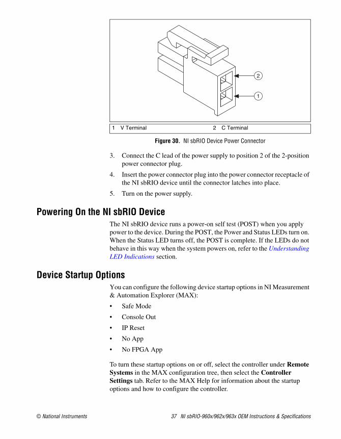
2. Connect the V lead of the power supply to position 1 of the power connector plug. Figure 30 shows the positions on the power connector.
DACGain andProtection
NI sbRIO - 9626/36 Analog Output
AO 10 V Nominal
AO GND
/–+
© National Instruments 37 NI sbRIO-960x/962x/963x OEM Instructions & Specifications
.
Figure 30. NI sbRIO Device Power Connector
3. Connect the C lead of the power supply to position 2 of the 2-position power connector plug.
4. Insert the power connector plug into the power connector receptacle of the NI sbRIO device until the connector latches into place.
5. Turn on the power supply.
Powering On the NI sbRIO DeviceThe NI sbRIO device runs a power-on self test (POST) when you apply power to the device. During the POST, the Power and Status LEDs turn on. When the Status LED turns off, the POST is complete. If the LEDs do not behave in this way when the system powers on, refer to the Understanding LED Indications section.
Device Startup OptionsYou can configure the following device startup options in NI Measurement & Automation Explorer (MAX):
• Safe Mode
• Console Out
• IP Reset
• No App
• No FPGA App
To turn these startup options on or off, select the controller under Remote Systems in the MAX configuration tree, then select the Controller Settings tab. Refer to the MAX Help for information about the startup options and how to configure the controller.
1 V Terminal 2 C Terminal
1
2
NI sbRIO-960x/962x/963x OEM Instructions & Specifications 38 ni.com
You can configure the device to launch an embedded stand-alone LabVIEW RT application each time it resets. Refer to the Running a Stand-Alone Real-Time Application (RT Module) topic of the LabVIEW Help for more information.
Device Reset OptionsYou can configure the device to launch a LabVIEW FPGA application each time it is reset. Table 8 lists the reset options available on the NI sbRIO device. These options determine how the FPGA behaves when the device is reset in various conditions. Use the RIO Device Setup utility to select reset options. Access the RIO Device Setup utility by selecting Start»All Programs»National Instruments»NI-RIO»RIO Device Setup.
Note If you want a VI to run when loaded to the FPGA, complete the following steps.
1. Right-click the FPGA Target item in the Project Explorer window in LabVIEW.
2. Select Properties.
3. In the General category of the FPGA Target Properties dialog box, place a check in the Run when loaded to FPGA checkbox.
4. Compile the FPGA VI.
Connecting the NI sbRIO Device to a NetworkConnect the device to an Ethernet network using the RJ-45 Ethernet port on the controller front panel. Use a standard Category 5 (CAT-5) or better shielded, twisted-pair Ethernet cable to connect the device to an Ethernet hub, or use an Ethernet crossover cable to connect the device directly to a computer.
Caution To prevent data loss and to maintain the integrity of your Ethernet installation, do not use a cable longer than 100 m.
Table 8. NI sbRIO Reset Options
Reset Option Behavior
Do not autoload VI Does not load the FPGA bit stream from flash memory.
Autoload VI on device powerup Loads the FPGA bit stream from flash memory to the FPGA when the device powers on.
Autoload VI on device reboot Loads the FPGA bit stream from flash memory to the FPGA when you reboot the device either with or without cycling power.
© National Instruments 39 NI sbRIO-960x/962x/963x OEM Instructions & Specifications
The first time you power up the device, it attempts to initiate a DHCP network connection. If the device is unable to initiate a DHCP connection, it connects to the network with a link-local IP address with the form 169.254.x.x. After powerup, you must install software on the device and configure the network settings in Measurement & Automation Explorer (MAX).
Note Installing software may change the network behavior of the device. For information about network behavior by installed software version, go to ni.com/info and enter the Info Code ipconfigcrio.
Connecting Serial DevicesNI sbRIO devices populated with RS-232 and RS-485 serial ports can connect to devices such as displays or input devices. Use the Serial VIs to read from and write to the serial port from a LabVIEW RT application. For more information about using the Serial VIs, refer to the Serial VIs and Functions topic of the LabVIEW Help.
Connecting CAN NetworksNI sbRIO devices populated with one IDC header provide connections to a CAN bus. CAN-enabled NI sbRIO devices have pins for CAN_H and CAN_L, which can connect to the CAN bus signals. The CAN port uses an NXP PCA82C251T high-speed CAN transceiver that is fully compatible with the ISO 11898 standard and supports baud rates up to 1 Mbps.
The port has two common pins (GND) that serve as the reference ground for CAN_H and CAN_L. You can connect the CAN bus reference ground (sometimes referred to as CAN_V–) to one or both COM pins. The port also has an optional shield pin (SHLD) that can connect to a shielded CAN cable. Connecting SHLD may improve signal integrity and EMC performance.
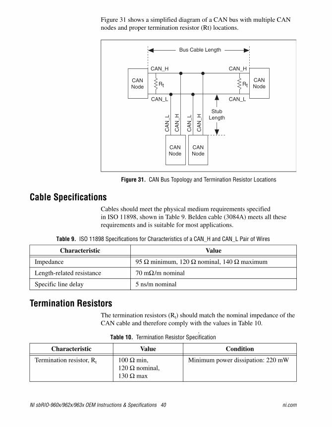
CAN Bus Topology and TerminationA CAN bus consists of two or more CAN nodes cabled together. The CAN_H and CAN_L pins of each node are connected to the main CAN bus cable through a short connection called a stub. The pair of signal wires, CAN_H and CAN_L, constitutes a transmission line. If the transmission line is not terminated, signal changes on the bus cause reflections that can cause communication errors. The CAN bus is bidirectional, and both ends of the cable must be terminated. This requirement does not mean that every node on the bus should have a termination resistor; only the two nodes at the far end of the cable should have termination resistors.
NI sbRIO-960x/962x/963x OEM Instructions & Specifications 40 ni.com
Figure 31 shows a simplified diagram of a CAN bus with multiple CAN nodes and proper termination resistor (Rt) locations.
Figure 31. CAN Bus Topology and Termination Resistor Locations
Cable SpecificationsCables should meet the physical medium requirements specified in ISO 11898, shown in Table 9. Belden cable (3084A) meets all these requirements and is suitable for most applications.
Termination ResistorsThe termination resistors (Rt) should match the nominal impedance of the CAN cable and therefore comply with the values in Table 10.
.
Table 9. ISO 11898 Specifications for Characteristics of a CAN_H and CAN_L Pair of Wires
Characteristic Value
Impedance 95 Ω minimum, 120 Ω nominal, 140 Ω maximum
Length-related resistance 70 mΩ /m nominal
Specific line delay 5 ns/m nominal
Table 10. Termination Resistor Specification
Characteristic Value Condition
Termination resistor, Rt 100 Ω min, 120 Ω nominal, 130 Ω max
Minimum power dissipation: 220 mW
CANNode
CANNode
CANNode
Rt Rt
CANNode
CAN_H
CAN_L
CAN_H
CAN_L
CA
N_H
CA
N_L
CA
N_H
CA
N_L
Bus Cable Length
StubLength
© National Instruments 41 NI sbRIO-960x/962x/963x OEM Instructions & Specifications
Cable LengthsThe cabling characteristics and desired bit transmission rates affect the allowable cable length. You can find detailed cable length recommendations in the ISO 11898, CiA DS 102, and DeviceNet specifications.
ISO 11898 specifies 40 m total cable length with a maximum stub length of 0.3 m for a bit rate of 1 Mb/s. The ISO 11898 specification allows for significantly longer cable lengths at lower bit rates, but each node should be analyzed for signal integrity problems.
Number of CAN NodesThe maximum number of nodes depends on the electrical characteristics of the nodes on the network. If all nodes meet the ISO 11898 requirements, you can connect at least 30 nodes to the bus. You can connect higher numbers of nodes if the electrical characteristics of the node do not degrade signal quality below ISO 11898 signal level specifications.
USB PortThis section applies only to the following NI sbRIO devices:
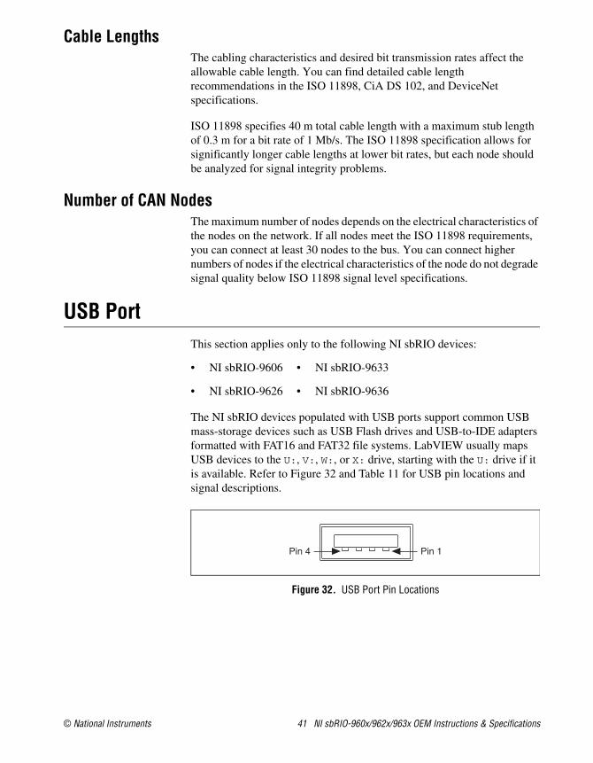
The NI sbRIO devices populated with USB ports support common USB mass-storage devices such as USB Flash drives and USB-to-IDE adapters formatted with FAT16 and FAT32 file systems. LabVIEW usually maps USB devices to the U:, V:, W:, or X: drive, starting with the U: drive if it is available. Refer to Figure 32 and Table 11 for USB pin locations and signal descriptions.
Figure 32. USB Port Pin Locations
• NI sbRIO-9606 • NI sbRIO-9633
• NI sbRIO-9626 • NI sbRIO-9636
Pin 1Pin 4
NI sbRIO-960x/962x/963x OEM Instructions & Specifications 42 ni.com
Using the System Clock to Provide Data TimestampsAt startup, the system clock of the NI sbRIO-9605/9606 resets to January 1, 1970, 12:00 a.m. (midnight), unless VBAT is implemented on the RMC.For information about synchronizing the system clock with an SNTP time server on the network at startup, go to ni.com/info and enter the Info Code criosntp.
Using the Reset ButtonPressing the Reset button reboots the processor. The FPGA continues to run unless you select the Autoload VI on device reboot boot option. Refer to the Device Reset Options section for more information.
Note To force the device into safe mode, hold the reset button down for 5 seconds, then release. The device will be in safe mode with output from the COM1 serial port enabled.
Table 11. USB Port Signal Descriptions
Pin Signal Name Signal Description
1 VCC Cable power (+5 V)
2 D– USB data–
3 D+ USB data+
4 GND Ground
© National Instruments 43 NI sbRIO-960x/962x/963x OEM Instructions & Specifications
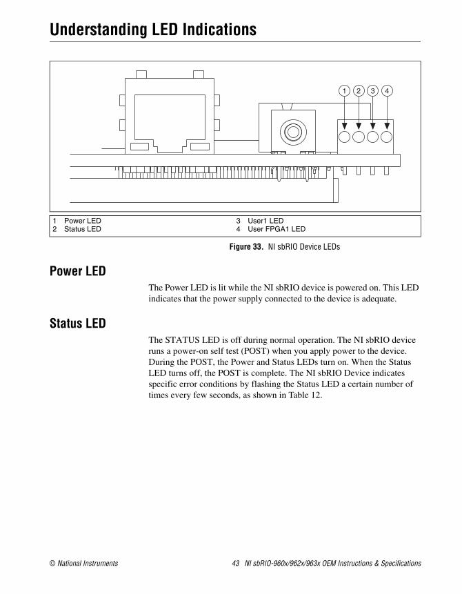
Understanding LED Indications
Figure 33. NI sbRIO Device LEDs
Power LEDThe Power LED is lit while the NI sbRIO device is powered on. This LED indicates that the power supply connected to the device is adequate.
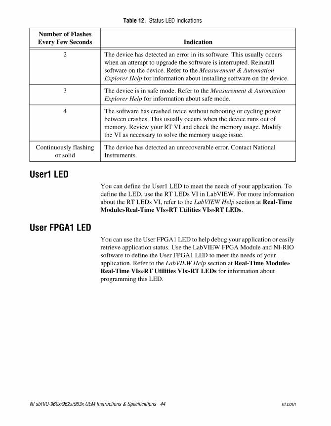
Status LEDThe STATUS LED is off during normal operation. The NI sbRIO device runs a power-on self test (POST) when you apply power to the device. During the POST, the Power and Status LEDs turn on. When the Status LED turns off, the POST is complete. The NI sbRIO Device indicates specific error conditions by flashing the Status LED a certain number of times every few seconds, as shown in Table 12.
1 Power LED2 Status LED
3 User1 LED4 User FPGA1 LED
3 421
NI sbRIO-960x/962x/963x OEM Instructions & Specifications 44 ni.com
User1 LEDYou can define the User1 LED to meet the needs of your application. To define the LED, use the RT LEDs VI in LabVIEW. For more information about the RT LEDs VI, refer to the LabVIEW Help section at Real-Time Module»Real-Time VIs»RT Utilities VIs»RT LEDs.
User FPGA1 LEDYou can use the User FPGA1 LED to help debug your application or easily retrieve application status. Use the LabVIEW FPGA Module and NI-RIO software to define the User FPGA1 LED to meet the needs of your application. Refer to the LabVIEW Help section at Real-Time Module»Real-Time VIs»RT Utilities VIs»RT LEDs for information about programming this LED.
Table 12. Status LED Indications
Number of Flashes Every Few Seconds Indication
2 The device has detected an error in its software. This usually occurs when an attempt to upgrade the software is interrupted. Reinstall software on the device. Refer to the Measurement & Automation Explorer Help for information about installing software on the device.
3 The device is in safe mode. Refer to the Measurement & Automation Explorer Help for information about safe mode.
4 The software has crashed twice without rebooting or cycling power between crashes. This usually occurs when the device runs out of memory. Review your RT VI and check the memory usage. Modify the VI as necessary to solve the memory usage issue.
Continuously flashing or solid
The device has detected an unrecoverable error. Contact National Instruments.
© National Instruments 45 NI sbRIO-960x/962x/963x OEM Instructions & Specifications
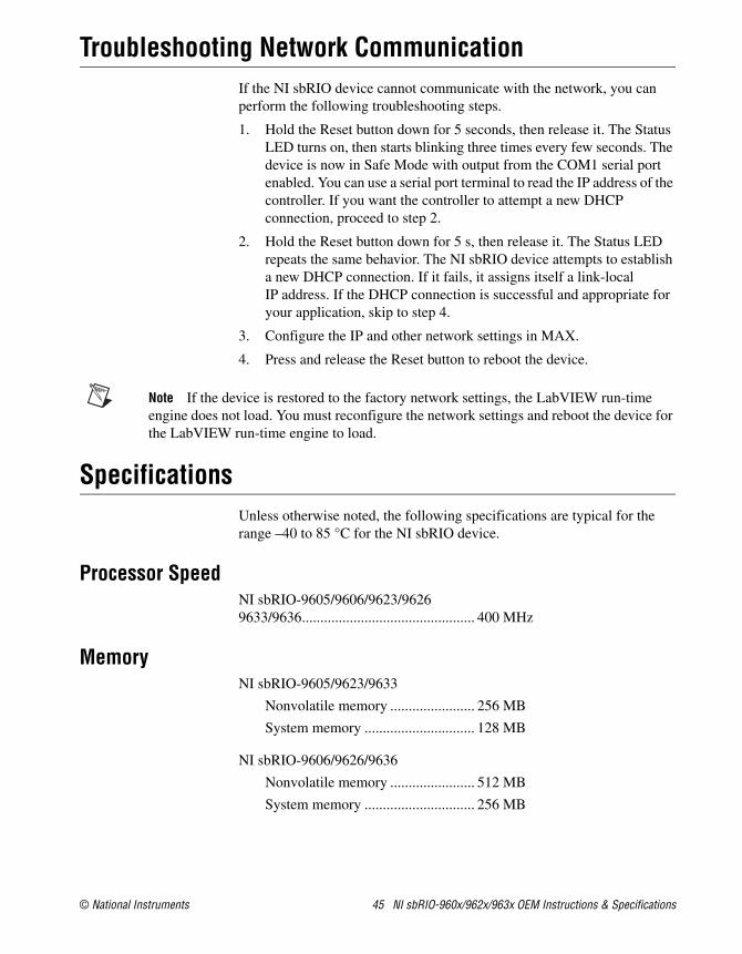
Troubleshooting Network CommunicationIf the NI sbRIO device cannot communicate with the network, you can perform the following troubleshooting steps.
1. Hold the Reset button down for 5 seconds, then release it. The Status LED turns on, then starts blinking three times every few seconds. The device is now in Safe Mode with output from the COM1 serial port enabled. You can use a serial port terminal to read the IP address of the controller. If you want the controller to attempt a new DHCP connection, proceed to step 2.
2. Hold the Reset button down for 5 s, then release it. The Status LED repeats the same behavior. The NI sbRIO device attempts to establish a new DHCP connection. If it fails, it assigns itself a link-local IP address. If the DHCP connection is successful and appropriate for your application, skip to step 4.
3. Configure the IP and other network settings in MAX.
4. Press and release the Reset button to reboot the device.
Note If the device is restored to the factory network settings, the LabVIEW run-time engine does not load. You must reconfigure the network settings and reboot the device for the LabVIEW run-time engine to load.
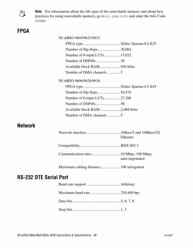
SpecificationsUnless otherwise noted, the following specifications are typical for the range –40 to 85 °C for the NI sbRIO device.
Processor SpeedNI sbRIO-9605/9606/9623/96269633/9636............................................... 400 MHz
MemoryNI sbRIO-9605/9623/9633
Nonvolatile memory ....................... 256 MB
System memory .............................. 128 MB
NI sbRIO-9606/9626/9636
Nonvolatile memory ....................... 512 MB
System memory .............................. 256 MB
NI sbRIO-960x/962x/963x OEM Instructions & Specifications 46 ni.com
Note For information about the life span of the nonvolatile memory and about best practices for using nonvolatile memory, go to ni.com/info and enter the Info Code SSDBP.
FPGANI sbRIO-9605/9623/9633
FPGA type .......................................Xilinx Spartan-6 LX25
Number of flip-flops........................30,064
Number of 6-input LUTs.................15,032
Number of DSP48s..........................38
Available block RAM......................936 kbits
Number of DMA channels ..............5
NI sbRIO-9606/9626/9636
FPGA type .......................................Xilinx Spartan-6 LX45
Number of flip-flops........................54,576
Number of 6-input LUTs.................27,288
Number of DSP48s..........................58
Available block RAM......................2,088 kbits
Number of DMA channels ..............5
NetworkNetwork interface ...................................10BaseT and 100BaseTX
Ethernet
Compatibility ..........................................IEEE 802.3
Communication rates ..............................10 Mbps, 100 Mbps, auto-negotiated
Maximum cabling distance.....................100 m/segment
RS-232 DTE Serial PortBaud rate support....................................Arbitrary
Maximum baud rate................................230,400 bps
Data bits ..................................................5, 6, 7, 8
Stop bits ..................................................1, 2
© National Instruments 47 NI sbRIO-960x/962x/963x OEM Instructions & Specifications
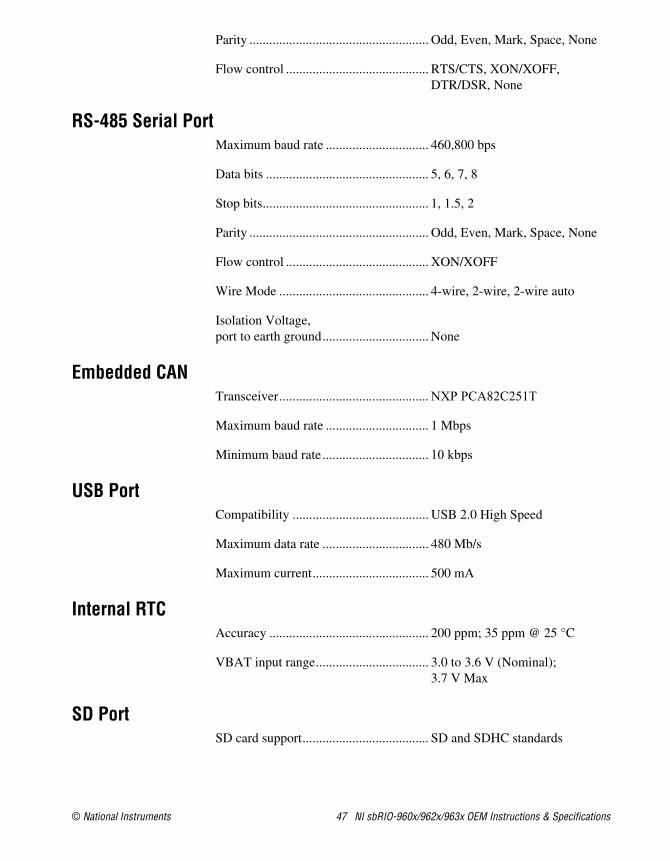
Parity ...................................................... Odd, Even, Mark, Space, None
Flow control ........................................... RTS/CTS, XON/XOFF, DTR/DSR, None
RS-485 Serial PortMaximum baud rate ............................... 460,800 bps
Data bits ................................................. 5, 6, 7, 8
Stop bits.................................................. 1, 1.5, 2
Parity ...................................................... Odd, Even, Mark, Space, None
Flow control ........................................... XON/XOFF
Wire Mode ............................................. 4-wire, 2-wire, 2-wire auto
Isolation Voltage, port to earth ground................................ None
Embedded CANTransceiver............................................. NXP PCA82C251T
Maximum baud rate ............................... 1 Mbps
Minimum baud rate ................................ 10 kbps
USB PortCompatibility ......................................... USB 2.0 High Speed
Maximum data rate ................................ 480 Mb/s
Maximum current................................... 500 mA
Internal RTCAccuracy ................................................ 200 ppm; 35 ppm @ 25 °C
VBAT input range.................................. 3.0 to 3.6 V (Nominal); 3.7 V Max
SD PortSD card support...................................... SD and SDHC standards
NI sbRIO-960x/962x/963x OEM Instructions & Specifications 48 ni.com
3.3 V Digital I/O on RIO Mezzanine Card ConnectorNumber of DIO channels........................96
Max tested current per channel...............±3 mA
Max total current, all lines ......................288 mA
Note The performance of the RMC DIO lines is bounded by the FPGA, signal integrity, the application timing requirements, and the RMC design. A general SPI application will typically be able to meet these requirements and achieve frequencies of up to 10 MHz. For more information on using DIO to connect to RMCs, go to ni.com/info and enter the Info Code RMCDIO.
Input logic levels
Input low voltage, VIL ......................0 V min; 0.8 V max
Input high voltage, VIH ....................2.0 V min; 3.465 V max
Output logic levels
Output high voltage, VOH
sourcing 3 mA .................................2.4 V min; 3.465 V max
Output low voltage, VOL
sinking 3 mA ...................................0.0 V min; 0.4 V max
3.3 V Digital I/O on 50-Pin IDC ConnectorNumber of DIO channels
NI sbRIO-9623/9626 .......................4
NI sbRIO-9633/9636 .......................28
Max tested current per channel...............±3 mA
Max total current, all lines
NI sbRIO-9623/9626 .......................12 mA
NI sbRIO-9633/9636 .......................84 mA
Input logic levels
Input low voltage, VIL ......................0 V min; 0.8 V max
Input high voltage, VIH ....................2.0 V min; 5.25 V max
Output logic levels
Output high voltage, VOH
sourcing 3 mA .................................2.4 V min; 3.465 V max
Output low voltage, VOL
sinking 3 mA ...................................0.0 V min; 0.4 V max
© National Instruments 49 NI sbRIO-960x/962x/963x OEM Instructions & Specifications
Analog Input Characteristics
NI sbRIO-9623/9633Number of channels ............................... 16 single-ended
ADC Resolution..................................... 12 bits
Maximum aggregate sampling rate........ 500 kS/s
Input range ............................................. 0–5 V nominal
Input impedance
Powered on, idle ............................. 250 MΩAcquiring 500 kS/s ......................... 325 kΩPowered off/overload...................... 1 kΩ
Overvoltage protection........................... None
AI accuracy
Note For information about measuring the local ambient temperature, refer to the Environmental section.
INL ......................................................... ±0.024% of range
DNL ....................................................... ±0.024% of range
Input bandwidth (-3 dB)......................... 6 MHz
NI sbRIO-9626/9636Number of channels ............................... 16 single-ended or 8 differential
ADC Resolution..................................... 16 bits
Maximum aggregate sampling rate........ 200 kS/s
Input range ............................................. ±10 V, ±5 V, ±2 V, ±1 V
Measurement Conditions
Percent of Reading (Gain Error)
Percent of Range* (Offset Error)
Typical (25 °C, ±5 °C) 0.11% 0.03%
Max (–40 to 85 °C) 0.55% 0.16%
* Range = 5 V
NI sbRIO-960x/962x/963x OEM Instructions & Specifications 50 ni.com
Maximum working voltage (signal + common mode)
Input impedance
Powered on ......................................> 1 GΩ in parallel with 100 pF
Powered off/overload ......................2.3 kΩ min
Overvoltage protection
Powered on ...................................... ±25 V, for up to 2 AI pins
Powered off ..................................... ±15V
AI accuracy
Gain drift.................................................12 ppm of reading/°C
Offset drift ..............................................4 ppm of range/°C
AI Noise
INL.......................................................... ±64 ppm of range, max
DNL ........................................................No missing codes guaranteed
Range Working voltage
10 V ±11 V
5 V ± 10.5 V
2 V ± 9 V
1 V ± 8.5 V
Measurement Conditions Range
Percent of Reading
(Gain Error)
Percent of Range
(Offset Error)
Typical (25 °C, ±5 °C)
1 V
0.042%
0.007%
2 V 0.007%
5 V 0.007%
10 V 0.008%
Max (–40 to 85 °C)
1 V 0.380% 0.179%
2 V 0.360% 0.138%
5 V 0.348% 0.113%
10 V 0.344% 0.105%
Range Working voltage
10 V 200 µVRMS
5 V 105 µVRMS
2 V 45 µVRMS
1 V 30 µVRMS
© National Instruments 51 NI sbRIO-960x/962x/963x OEM Instructions & Specifications
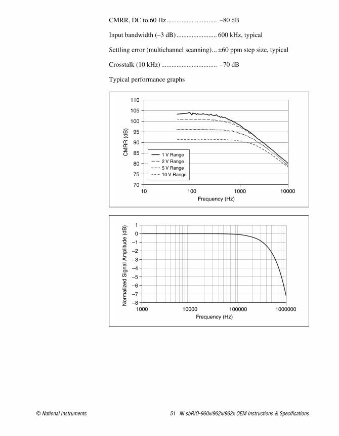
CMRR, DC to 60 Hz.............................. –80 dB
Input bandwidth (–3 dB) ........................ 600 kHz, typical
Settling error (multichannel scanning)... ±60 ppm step size, typical
Crosstalk (10 kHz) ................................. –70 dB
Typical performance graphs
CM
RR
(dB
)
Frequency (Hz)10 100 1000 10000
110
100
105
90
95
85
80
70
75
1 V Range2 V Range5 V Range10 V Range
Nor
mal
ized
Sig
nal A
mpl
itude
(dB
)
Frequency (Hz)1000 10000 100000 1000000
1
–2
–4
–7
–8
–6
–5
–3
–1
0
NI sbRIO-960x/962x/963x OEM Instructions & Specifications 52 ni.com
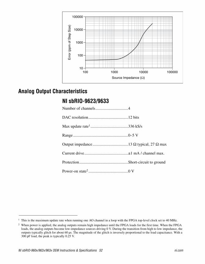
Analog Output Characteristics
NI sbRIO-9623/9633Number of channels................................4
DAC resolution.......................................12 bits
Max update rate1 .....................................336 kS/s
Range ......................................................0–5 V
Output impedance...................................13 Ω typical, 27 Ω max
Current drive...........................................±1 mA / channel max.
Protection................................................Short-circuit to ground
Power-on state2 .......................................0 V
1 This is the maximum update rate when running one AO channel in a loop with the FPGA top-level clock set to 40 MHz.2 When power is applied, the analog outputs remain high impedance until the FPGA loads for the first time. When the FPGA
loads, the analog outputs become low-impedance sources driving 0 V. During the transition from high to low impedance, the outputs typically glitch for about 60 µs. The magnitude of the glitch is inversely proportional to the load capacitance. With a 300 pF load, the peak is typically 0.25 V.
Err
or (
ppm
of S
tep
Siz
e)
Source Impedance (Ω)
100 1000 10000 100000
100000
10000
1000
100
10
© National Instruments 53 NI sbRIO-960x/962x/963x OEM Instructions & Specifications
AO accuracy
Note For information about measuring the local ambient temperature, refer to the Environmental section.
INL ......................................................... ±0.018% of range, max
Capacitive drive ..................................... 1 nF, typical
Slew rate................................................. 0.75 V / µsec, typical
NI sbRIO-9626/9636Number of channels ............................... 4
DAC resolution ...................................... 16 bits
Max update rate1 .................................... 336 kS/s
Range ..................................................... ±10 V
Overrange operating voltage
Minimum ........................................ 10.3 V
Typical ............................................ 10.6 V
Max ................................................. 10.9 V
Output impedance .................................. 0.4 Ω typical
Current drive .......................................... ±3 mA / channel max.
Protection ............................................... Short-circuit to ground
Power-on state2 ...................................... 0 V
Measurement ConditionsPercent of Reading
(Gain Error)Percent of Range*
(Offset Error)
Typical (25 °C, ±5 °C) 0.12% 0.02%
Max (–40 to 85 °C) 0.80% 0.12%
* Range is 5 V.
1 This is the maximum update rate when running one AO channel in a loop with the FPGA top-level clock set to 40 MHz.2 When the analog output initializes, a glitch occurs for about 20 µs, peaking at 1.3 V, typical.
NI sbRIO-960x/962x/963x OEM Instructions & Specifications 54 ni.com
AO accuracy
Gain drift.................................................23 ppm of reading/°C
Offset drift ..............................................5.4 ppm of range/°C
INL..........................................................±194 ppm of range, max
DNL ........................................................±16 ppm of range, max
Capacitive drive ......................................1.5 nF, typical
Slew rate .................................................3.7 V / µsec, typical
Settling time (100 pF load to 320 μV)
FS step .............................................50 μs
2 V step............................................12 μs
0.2 V step.........................................9 μs
Power RequirementsThe NI sbRIO device requires a power supply connected to the power connector. Refer to Figure 2 for the location of the power connector. Refer to the Powering the NI sbRIO Device section for information about connecting the power supply.
Caution Exceeding the power limits may cause unpredictable behavior by the device.
Recommended power supply..................55 W, 30 VDC max
Power supply voltage range....................9–30 VDC1
Measurement ConditionsPercent of Reading
(Gain Error)Percent of Range*
(Offset Error)
Typical (25 °C, ±5 °C) 0.09% 0.02%
Max (–40 to 85 °C) 0.50% 0.20%
* Range is 10 V.
1 The NI sbRIO device is 1–2% more efficient with a 9 V power supply than with a 30 V power supply.
© National Instruments 55 NI sbRIO-960x/962x/963x OEM Instructions & Specifications
The total power required by the NI sbRIO device from its power supply depends heavily on how it is being used, and can be approximated by the following calculations:
Total power requirement = Pint + PDIO + P5V + PUSB
where Pint is the power consumption by the NI sbRIO device internal operation, including integrated I/O functions
PDIO is the power consumption by the 3.3 V DIO lines across the RMC, MIO, or DIO connectors
P5V is the power consumption by the 5 V voltage output across the RMC or MIO connectors
P3.3V is the power consumption by the 3.3 V voltage output across the RMC Connector
PUSB is the power consumption of a device plugged into the USB port
PSD is the power consumption of an SD card plugged into the SD slot
PAO is the power consumption of the Analog output across the MIO connector
When calculating each component of the maximum power consumption the following efficiency factors must be used:
η3.3 V, ηDIO and ηSD = 80%
η5 V and ηUSB = 90%
ηAO = 50%
PAO is the power consumption of the Analog output across the MIO connector
Note You must add 10% to the calculated or measured total power requirement to account for transient and startup conditions.
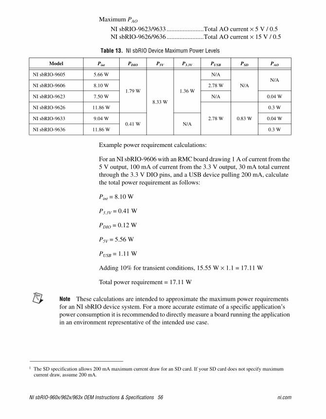
Maximum Pint......................................... Refer to Table 13.
Maximum PDIO....................................... Total DIO current × 3.3 V / 0.8
Maximum P5V ........................................ Total 5 V current × 5 V / 0.9
Maximum P3.3V ...................................... Total 3.3 V current × 3.3 V / 0.8
Maximum PUSB ...................................... Total USB current × 5 V / 0.9
Maximum PSD1....................................... Total SD current × 3.3 V / 0.8
NI sbRIO-960x/962x/963x OEM Instructions & Specifications 56 ni.com
Maximum PAO
NI sbRIO-9623/9633 .......................Total AO current × 5 V / 0.5 NI sbRIO-9626/9636 .......................Total AO current × 15 V / 0.5
Example power requirement calculations:
For an NI sbRIO-9606 with an RMC board drawing 1 A of current from the 5 V output, 100 mA of current from the 3.3 V output, 30 mA total current through the 3.3 V DIO pins, and a USB device pulling 200 mA, calculate the total power requirement as follows:
Pint = 8.10 W
P3.3V = 0.41 W
PDIO = 0.12 W
P5V = 5.56 W
PUSB = 1.11 W
Adding 10% for transient conditions, 15.55 W × 1.1 = 17.11 W
Total power requirement = 17.11 W
Note These calculations are intended to approximate the maximum power requirements for an NI sbRIO device system. For a more accurate estimate of a specific application’s power consumption it is recommended to directly measure a board running the application in an environment representative of the intended use case.
1 The SD specification allows 200 mA maximum current draw for an SD card. If your SD card does not specify maximum current draw, assume 200 mA.
Table 13. NI sbRIO Device Maximum Power Levels
Model Pint PDIO P5V P3.3V PUSB PSD PAO
NI sbRIO-9605 5.66 W
1.79 W
8.33 W
1.36 W
N/A
N/AN/A
NI sbRIO-9606 8.10 W 2.78 W
NI sbRIO-9623 7.50 W N/A 0.04 W
NI sbRIO-9626 11.86 W
2.78 W 0.83 W
0.3 W
NI sbRIO-9633 9.04 W0.41 W N/A
0.04 W
NI sbRIO-9636 11.86 W 0.3 W
© National Instruments 57 NI sbRIO-960x/962x/963x OEM Instructions & Specifications
NI sbRIO-9605
Power consumption whilesourcing RMC................................. 19.1 W Max
NI sbRIO-9606
Power consumption whilesourcing RMC................................. 25.4 W Max
NI sbRIO-9623
Power consumption whilesourcing RMC................................. 21.7 W Max
NI sbRIO-9626
Power consumption whilesourcing RMC................................. 29.9 W Max
NI sbRIO-9633
Power consumption......................... 21.9 W Max
NI sbRIO-9636
Power consumption......................... 24.7 W Max
EnvironmentalThe NI sbRIO device is intended for indoor use only.
Local ambient temperature near device(IEC 60068-2-1, IEC 60068-2-2)
NI sbRIO-960x ............................... –40 to 85 °C
NI sbRIO-962x ............................... –40 to 85 °C
NI sbRIO-963x ............................... –40 to 85 °C
Note Measure the local ambient temperature by placing thermocouples on both sides of the PCB, 0.2 in. (5 mm) from the board surface. Avoid placing thermocouples next to hot components such as the FPGA, processor, or near board edges, which can cause inaccurate temperature measurements. In addition to the local ambient temperature, the case temperature of the components should not exceed the recommended maximum case temperature.
NI sbRIO-960x/962x/963x OEM Instructions & Specifications 58 ni.com
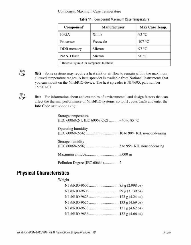
Component Maximum Case Temperature
Note Some systems may require a heat sink or air flow to remain within the maximum allowed temperature ranges. A heat spreader is available from National Instruments that you can mount on the NI sbRIO device. The heat spreader is NI 9695, part number 153901-01.
Note For information about and examples of environmental and design factors that can affect the thermal performance of NI sbRIO systems, so to ni.com/info and enter the Info Code sbriocooling.
Storage temperature(IEC 60068-2-1, IEC 60068-2-2) ...........–40 to 85 °C
Operating humidity(IEC 60068-2-56) ...................................10 to 90% RH, noncondensing
Storage humidity(IEC 60068-2-56) ...................................5 to 95% RH, noncondensing
Maximum altitude...................................5,000 m
Pollution Degree (IEC 60664) ................2
Physical CharacteristicsWeight
NI sbRIO-9605 ................................85 g (2.998 oz)
NI sbRIO-9606 ................................89 g (3.139 oz)
NI sbRIO-9623 ................................123 g (4.24 oz)
NI sbRIO-9626 ................................133 g (4.69 oz)
NI sbRIO-9633 ................................131 g (4.62 oz)
NI sbRIO-9636 ................................132 g (4.66 oz)
Table 14. Component Maximum Case Temperature
Component* Manufacturer Max Case Temp.
FPGA Xilinx 93 °C
Processor Freescale 107 °C
DDR memory Micron 97 °C
NAND flash Micron 90 °C
* Refer to Figure 2 for component locations

© National Instruments 59 NI sbRIO-960x/962x/963x OEM Instructions & Specifications
Safety VoltagesConnect only voltages that are within this limit.
V terminal to C terminal ........................ 30 VDC max, Measurement Category I
Measurement Category I is for measurements performed on circuits not directly connected to the electrical distribution system referred to as MAINS voltage. MAINS is a hazardous live electrical supply system that powers equipment. This category is for measurements of voltages from specially protected secondary circuits. Such voltage measurements include signal levels, special equipment, limited-energy parts of equipment, circuits powered by regulated low-voltage sources, and electronics.
Caution Do not connect the system to signals or use for measurements within Measurement Categories II, III, or IV.
Environmental ManagementNI is committed to designing and manufacturing products in an environmentally responsible manner. NI recognizes that eliminating certain hazardous substances from our products is beneficial to the environment and to NI customers.
For additional environmental information, refer to the NI and the Environment Web page at ni.com/environment. This page contains the environmental regulations and directives with which NI complies, as well as other environmental information not included in this document.
Waste Electrical and Electronic Equipment (WEEE)EU Customers At the end of the product life cycle, all products must be sent to a WEEE recycling center. For more information about WEEE recycling centers, National Instruments WEEE initiatives, and compliance with WEEE Directive 2002/96/EC on Waste and Electronic Equipment, visit ni.com/environment/weee.
RoHSNational Instruments (RoHS)
National Instruments RoHS ni.com/environment/rohs_china(For information about China RoHS compliance, go to ni.com/environment/rohs_china.)
LabVIEW, National Instruments, NI, ni.com, the National Instruments corporate logo, and the Eagle logo are trademarks of National Instruments Corporation. Refer to the Trademark Information at ni.com/trademarks for other National Instruments trademarks. Other product and company names mentioned herein are trademarks or trade names of their respective companies. For patents covering National Instruments products/technology, refer to the appropriate location: Help»Patents in your software, the patents.txt file on your media, or the National Instruments Patent Notice at ni.com/patents. Refer to the Export Compliance Information at ni.com/legal/export-compliance for the National Instruments global trade compliance policy and how to obtain relevant HTS codes, ECCNs, and other import/export data.
© 2012 National Instruments. All rights reserved. 373378C-01 Aug 12
Where to Go for SupportThe National Instruments Web site is your complete resource for technical support. At ni.com/support you have access to everything from troubleshooting and application development self-help resources to email and phone assistance from NI Application Engineers.
National Instruments corporate headquarters is located at 11500 North Mopac Expressway, Austin, Texas, 78759-3504. National Instruments also has offices located around the world to help address your support needs. For telephone support in the United States, create your service request at ni.com/support and follow the calling instructions or dial 512 795 8248. For telephone support outside the United States, visit the Worldwide Offices section of ni.com/niglobal to access the branch office Web sites, which provide up-to-date contact information, support phone numbers, email addresses, and current events.