NI PXIe-5160 Specifications - National...
24
DEVICE SPECIFICATIONS NI PXIe-5160 2.5 GS/s, 10-Bit Digitizer This document lists the specifications for the NI PXIe-5160, 500 MHz digitizer. Unless otherwise noted, the following conditions were used for each specification: • All vertical ranges • All bandwidths and bandwidth limit filters • Sample rate set to 1.25 GS/s or 2.5 GS/s • Onboard Sample clock locked to onboard Reference clock Warranted specifications describe the warranted, traceable product performance over ambient temperature ranges of 0 °C to 45 °C and include guardband for measurement uncertainty, unless otherwise noted. Specifications are warranted under the following conditions: • The NI 5160 module is warmed up for 15 minutes at ambient temperature • Self-calibration is completed after warm-up period • Calibration cycle is maintained • The PXI Express chassis fan speed is set to HIGH, the foam fan filters are removed if present, and the empty slots contain PXI chassis slot blockers and filler panels. For more information about cooling, refer to the Maintain Forced-Air Cooling Note to Users document available at ni.com/manuals. • NI-SCOPE 4.1 or later instrument driver is used • External calibration is performed at 23 °C ± 3 °C Typical specifications are unwarranted values that are representative of measurements taken during development or production and cover the expected performance of units over ambient temperature ranges of 0 °C to 45 °C with a 90% confidence level. Characteristic values (or supplemental information) describe additional information about the product that may be useful, including expected performance that is not covered under Warranted or Typical values. Specifications are subject to change without notice. For the most recent NI 5160 specifications, visit ni.com/manuals. To access the NI 5160 documentation, including the NI High-Speed Digitizers Getting Started Guide, go to Start»All Programs»National Instruments»NI-SCOPE»Documentation. In Windows 8, click NI Launcher and select NI-SCOPE in the window that appears.
Transcript of NI PXIe-5160 Specifications - National...
DEVICE SPECIFICATIONS
NI PXIe-51602.5 GS/s, 10-Bit Digitizer
This document lists the specifications for the NI PXIe-5160, 500 MHz digitizer.
Unless otherwise noted, the following conditions were used for each specification:• All vertical ranges• All bandwidths and bandwidth limit filters• Sample rate set to 1.25 GS/s or 2.5 GS/s• Onboard Sample clock locked to onboard Reference clock
Warranted specifications describe the warranted, traceable product performance over ambienttemperature ranges of 0 °C to 45 °C and include guardband for measurement uncertainty,unless otherwise noted. Specifications are warranted under the following conditions:• The NI 5160 module is warmed up for 15 minutes at ambient temperature• Self-calibration is completed after warm-up period• Calibration cycle is maintained• The PXI Express chassis fan speed is set to HIGH, the foam fan filters are removed if
present, and the empty slots contain PXI chassis slot blockers and filler panels. For moreinformation about cooling, refer to the Maintain Forced-Air Cooling Note to Usersdocument available at ni.com/manuals.
• NI-SCOPE 4.1 or later instrument driver is used• External calibration is performed at 23 °C ± 3 °C
Typical specifications are unwarranted values that are representative of measurements takenduring development or production and cover the expected performance of units over ambienttemperature ranges of 0 °C to 45 °C with a 90% confidence level.
Characteristic values (or supplemental information) describe additional information about theproduct that may be useful, including expected performance that is not covered underWarranted or Typical values.
Specifications are subject to change without notice. For the most recent NI 5160specifications, visit ni.com/manuals.
To access the NI 5160 documentation, including the NI High-Speed Digitizers Getting StartedGuide, go to Start»All Programs»National Instruments»NI-SCOPE»Documentation. InWindows 8, click NI Launcher and select NI-SCOPE in the window that appears.
Caution To ensure the specified EMC performance, operate this product only withdouble-shielded cables (for example, RG-223/U) and accessories.
Caution The protection provided by the NI 5160 can be impaired if it is used in amanner not described in this document.
ContentsAnalog Input............................................................................................................................. 3
Impedance and Coupling.................................................................................................. 3Voltage Levels...................................................................................................................3Accuracy........................................................................................................................... 5Bandwidth and Transient Response.................................................................................. 5Spectral Characteristics.....................................................................................................9
Horizontal................................................................................................................................11Sample Clock.................................................................................................................. 11Phase-Locked Loop (PLL) Reference Clock.................................................................. 12External Sample Clock (CLK IN, Front Panel Connector)............................................ 12External Reference Clock In (CLK IN, Front Panel Connector)....................................13Reference Clock Out (CLK OUT, Front Panel Connector)............................................ 13
Trigger.....................................................................................................................................13Analog Trigger (Edge Trigger Type).............................................................................. 14External Trigger (TRIG, Front Panel Connector)........................................................... 14Digital Trigger (Digital Trigger Type)............................................................................ 15Programmable Function Interface (PFI 0 and PFI 1, Front Panel Connectors)..............15
Waveform Specifications........................................................................................................ 16Memory Sanitization...............................................................................................................16Calibration...............................................................................................................................16
External Calibration........................................................................................................ 16Self-Calibration...............................................................................................................16Calibration Specifications............................................................................................... 17
Power...................................................................................................................................... 17Software.................................................................................................................................. 17
Driver Software...............................................................................................................17Application Software...................................................................................................... 17Interactive Soft Front Panel and Configuration.............................................................. 17TClk Specifications.........................................................................................................17
Physical................................................................................................................................... 18Front Panel Connectors...................................................................................................18Dimensions and Weight.................................................................................................. 19
Environment............................................................................................................................21Operating Environment...................................................................................................21Storage Environment.......................................................................................................21
Shock and Vibration................................................................................................................21Compliance and Certifications................................................................................................22
Safety.............................................................................................................................. 22Electromagnetic Compatibility....................................................................................... 22CE Compliance .............................................................................................................. 22
2 | ni.com | NI PXIe-5160 Specifications
Online Product Certification........................................................................................... 22Environmental Management........................................................................................... 23
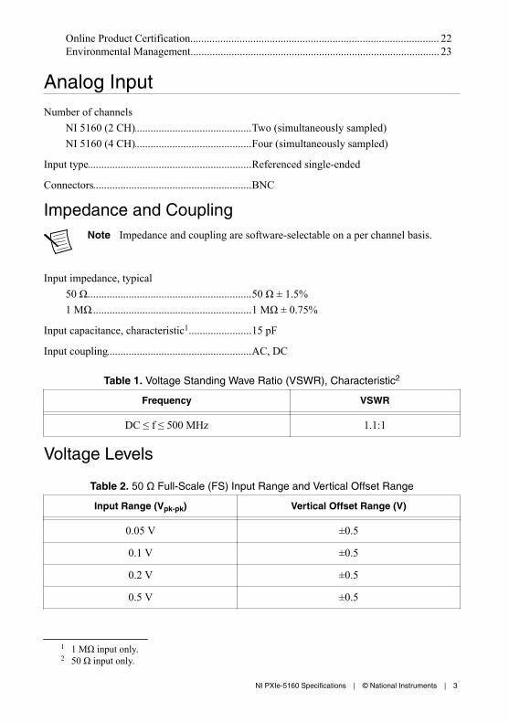
Analog InputNumber of channels
....................................................................NI 5160 (2 CH) Two (simultaneously sampled)
....................................................................NI 5160 (4 CH) Four (simultaneously sampled)
............................................................................Input type Referenced single-ended
............................................................................Connectors BNC
Impedance and CouplingNote Impedance and coupling are software-selectable on a per channel basis.
Input impedance, typical....................................................................50 Ω 50 Ω ± 1.5%....................................................................1 MΩ 1 MΩ ± 0.75%
............................................................................Input capacitance, characteristic1 15 pF
............................................................................Input coupling AC, DC
Table 1. Voltage Standing Wave Ratio (VSWR), Characteristic2
Frequency VSWR
DC ≤ f ≤ 500 MHz 1.1:1
Voltage Levels
Table 2. 50 Ω Full-Scale (FS) Input Range and Vertical Offset Range
Input Range (Vpk-pk) Vertical Offset Range (V)
0.05 V ±0.5
0.1 V ±0.5
0.2 V ±0.5
0.5 V ±0.5
1 1 MΩ input only.2 50 Ω input only.
NI PXIe-5160 Specifications | © National Instruments | 3
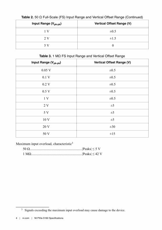
Table 2. 50 Ω Full-Scale (FS) Input Range and Vertical Offset Range (Continued)
Input Range (Vpk-pk) Vertical Offset Range (V)
1 V ±0.5
2 V ±1.5
5 V 0
Table 3. 1 MΩ FS Input Range and Vertical Offset Range
Input Range (Vpk-pk) Vertical Offset Range (V)
0.05 V ±0.5
0.1 V ±0.5
0.2 V ±0.5
0.5 V ±0.5
1 V ±0.5
2 V ±5
5 V ±5
10 V ±5
20 V ±30
50 V ±15
Maximum input overload, characteristic3
....................................................................50 Ω |Peaks| ≤ 5 V
....................................................................1 MΩ |Peaks| ≤ 42 V
3 Signals exceeding the maximum input overload may cause damage to the device.
4 | ni.com | NI PXIe-5160 Specifications
Accuracy
............................................................................Resolution 10 bits
............................................................................DC accuracy4 ±[(2% × |Reading - Vertical Offset|)+ (1.4% × |Vertical Offset|)+ (0.6% of FS) + 600 µV]
............................................................................DC drift, characteristic5 ±[(0.1% × |Reading - Vertical Offset|)+ (0.025% × |Vertical Offset|)+ (0.03% of FS)] per °C
............................................................................AC amplitude accuracy4 ±0.5 dB at 50 kHz
............................................................................AC amplitude drift, characteristic5 ±0.01 dB per °C at 50 kHz
Table 4. Crosstalk (CH to/from CH), Characteristic6
Input Impedance Input Frequency Crosstalk
50 Ω
DC ≤ f ≤ 100 MHz -60 dB
100 MHz < f ≤ 500 MHz -45 dB
1 MΩ7DC ≤ f ≤ 100 MHz -55 dB
100 MHz < f ≤ 200 MHz -45 dB
Bandwidth and Transient Response
Bandwidth (-3 dB)8
....................................................................50 Ω, typical 500 MHz
....................................................................1 MΩ, characteristic9 300 MHz
............................................................................Bandwidth-limiting filters 20 MHz, 175 MHz
4 Within ±3 °C of self-calibration temperature. This specification is typical for peak-to-peak input ranges of 0.05 V to 0.1 V and warranted for all other input ranges.
5 Used to calculate errors when onboard temperature changes more than ±3 °C from theself-calibration temperature.
6 Measured on one channel with test signal applied to another channel, with same range setting onboth channels.
7 Only valid on peak-to-peak input ranges of 0.05 V to 10 V.8 Normalized to 50 kHz.9 Verified using a 50 Ω source and 50 Ω feed-through terminator.
NI PXIe-5160 Specifications | © National Instruments | 5
Rise/fall time, typical10
....................................................................50 Ω 750 ps
....................................................................1 MΩ9 1.4 ns
AC-coupling cutoff (-3 dB)11
....................................................................50 Ω12 170 kHz
....................................................................1 MΩ 17 Hz
Figure 1. NI 5160 Step Response, 50 Ω, 1 Vpk-pk Input Range, -0.25 V ProgrammableOffset, 500 ps Rising Edge, Characteristic
Vol
ts
0.10
–0.55
–0.50
–0.45
–0.40
–0.35
–0.30
–0.25
–0.20
–0.15
–0.10
–0.05
0.00
0.05
Time (ns)
8–2 –1 0 1 2 3 4 5 6 7
10 50% FS input pulse.11 Verified using a 50 Ω source.12 With AC coupling enabled, the DC resistance to ground is 20 kΩ.
6 | ni.com | NI PXIe-5160 Specifications
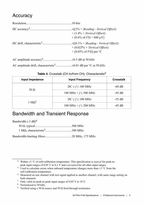
Figure 2. NI 5160 Step Response, 1 MΩ, 1 Vpk-pk Input Range, -0.25 V ProgrammableOffset, 500 ps Rising Edge, Characteristic13
Vol
ts0.10
–0.55
–0.50
–0.45
–0.40
–0.35
–0.30
–0.25
–0.20
–0.15
–0.10
–0.05
0.00
0.05
Time (ns) 7–2 –1 0 1 2 3 4 5 6
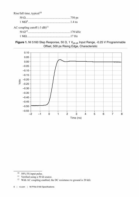
Figure 3. NI 5160 50 Ω Frequency Response, 1 Vpk-pk, 2.5 GS/s, Characteristic
Frequency (Hz)1 G1 M 100 M 200 M 300 M 400 M 500 M 600 M 700 M 800 M 900 M
1
–19
–17
–15
–13
–11
–9
–7
–5
–3
–1
Nor
mal
ized
Am
plitu
de (
dB)
13 Verified using a 50 Ω source and 50 Ω feed-through terminator.
NI PXIe-5160 Specifications | © National Instruments | 7
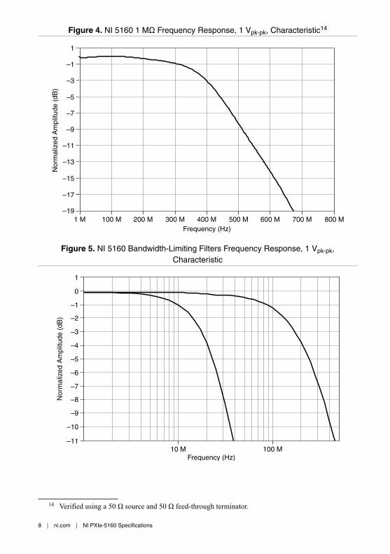
Figure 4. NI 5160 1 MΩ Frequency Response, 1 Vpk-pk, Characteristic14
Nor
mal
ized
Am
plitu
de (
dB)
1
–19
–17
–15
–13
–11
–9
–7
–5
–3
–1
Frequency (Hz)800 M1 M 100 M 200 M 300 M 400 M 500 M 600 M 700 M
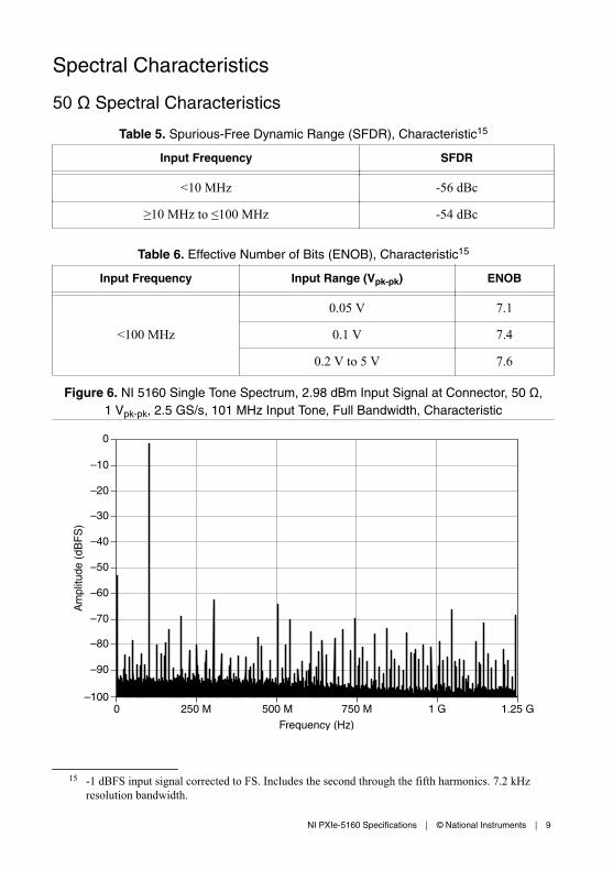
Figure 5. NI 5160 Bandwidth-Limiting Filters Frequency Response, 1 Vpk-pk,Characteristic
1
–11
–10
–9
–8
–7
–6
–5
–4
–3
–2
–1
0
Frequency (Hz)10 M 100 M
Nor
mal
ized
Am
plitu
de (
dB)
14 Verified using a 50 Ω source and 50 Ω feed-through terminator.
8 | ni.com | NI PXIe-5160 Specifications
Spectral Characteristics
50 Ω Spectral Characteristics
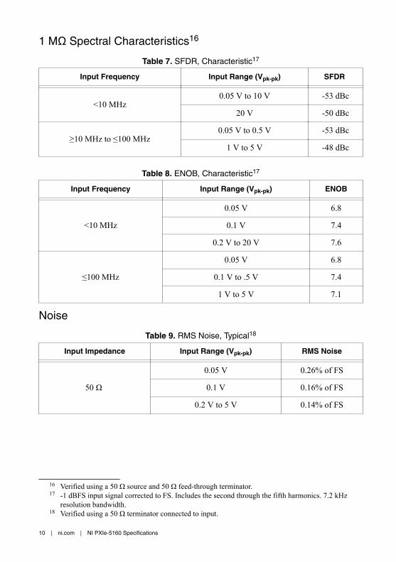
Table 5. Spurious-Free Dynamic Range (SFDR), Characteristic15
Input Frequency SFDR
<10 MHz -56 dBc
≥10 MHz to ≤100 MHz -54 dBc
Table 6. Effective Number of Bits (ENOB), Characteristic15
Input Frequency Input Range (Vpk-pk) ENOB
<100 MHz
0.05 V 7.1
0.1 V 7.4
0.2 V to 5 V 7.6
Figure 6. NI 5160 Single Tone Spectrum, 2.98 dBm Input Signal at Connector, 50 Ω,1 Vpk-pk, 2.5 GS/s, 101 MHz Input Tone, Full Bandwidth, Characteristic
0
–100
–90
–80
–70
–60
–50
–40
–30
–20
–10
1.25 G0 250 M 500 M 750 M 1 G
Am
plitu
de (
dBF
S)
Frequency (Hz)
15 -1 dBFS input signal corrected to FS. Includes the second through the fifth harmonics. 7.2 kHzresolution bandwidth.
NI PXIe-5160 Specifications | © National Instruments | 9
1 MΩ Spectral Characteristics16
Table 7. SFDR, Characteristic17
Input Frequency Input Range (Vpk-pk) SFDR
<10 MHz
0.05 V to 10 V -53 dBc
20 V -50 dBc
≥10 MHz to ≤100 MHz0.05 V to 0.5 V -53 dBc
1 V to 5 V -48 dBc
Table 8. ENOB, Characteristic17
Input Frequency Input Range (Vpk-pk) ENOB
<10 MHz
0.05 V 6.8
0.1 V 7.4
0.2 V to 20 V 7.6
≤100 MHz
0.05 V 6.8
0.1 V to .5 V 7.4
1 V to 5 V 7.1
Noise
Table 9. RMS Noise, Typical18
Input Impedance Input Range (Vpk-pk) RMS Noise
50 Ω
0.05 V 0.26% of FS
0.1 V 0.16% of FS
0.2 V to 5 V 0.14% of FS
16 Verified using a 50 Ω source and 50 Ω feed-through terminator.17 -1 dBFS input signal corrected to FS. Includes the second through the fifth harmonics. 7.2 kHz
resolution bandwidth.18 Verified using a 50 Ω terminator connected to input.
10 | ni.com | NI PXIe-5160 Specifications
Table 9. RMS Noise, Typical18 (Continued)
Input Impedance Input Range (Vpk-pk) RMS Noise
1 MΩ
0.05 V 0.26% of FS
0.1 V 0.16% of FS
0.2 V to 50 V 0.14% of FS
Skew
Channel-to-channel skew, characteristic....................................................................50 Ω to 50 Ω <25 ps....................................................................1 MΩ to 1 MΩ <125 ps....................................................................50 Ω to 1 MΩ <800 ps
Horizontal
Sample Clock
Sources....................................................................Internal Onboard clock (internal VCO)....................................................................External Front panel SMB connector
Onboard Clock
Real-time sample rate range19
....................................................................One channel enabled 76.299 kS/s to 2.5 GS/s
....................................................................Two channels enabled20 76.299 kS/s to 2.5 GS/s
....................................................................Four channels enabled 76.299 kS/s to 1.25 GS/s
19 Divide by n decimation from 1.25 GS/s used for all rates less than 1.25 GS/s. For more informationabout the Sample Clock and decimation, refer to the NI High-Speed Digitizers Help.
20 For the NI 5160 (4 CH), supported on channels 0 and 2. For the NI 5160 (2 CH),supported on channels 0 and 1.
NI PXIe-5160 Specifications | © National Instruments | 11
............................................................................Random Interleaved Sampling (RIS)range21
Up to 50 GS/s
............................................................................Sample clock jitter, characteristic22 250 fs RMS (12 kHz to 10 MHz)
............................................................................Timebase frequency 2.5 GHz
............................................................................Timebase accuracy, typical ±10 ppm
Phase-Locked Loop (PLL) Reference Clock
Sources....................................................................Internal Onboard 10 MHz reference or PXI_CLK10
(backplane connector)....................................................................External External 10 MHz at front panel CLK IN
connector
............................................................................Duty cycle tolerance 45% to 55%
External Sample Clock (CLK IN, Front PanelConnector)
............................................................................Input voltage range, when configuredas a Sample Clock
-10 dBm through 16 dBm
............................................................................Maximum input overload, whenconfigured as a Sample Clock
18 dBm
............................................................................Impedance 50 Ω
............................................................................Coupling AC
............................................................................Frequency range 1.25 GHz to 2.5 GHz23
21 With one channel enabled, stepped in multiples of 2.5 GS/s. With two channels enabled,stepped in multiples of 2.5 GS/s. With four channels enabled, stepped in multiples of1.25 GS/s.
22 Includes the effects of the converter aperture uncertainty and the clock circuitry jitter.Excludes trigger jitter.
23 To achieve the same real-time sample rate ranges as the onboard clock, a 2.5 GHz frequency isrequired.
12 | ni.com | NI PXIe-5160 Specifications
External Reference Clock In (CLK IN, Front PanelConnector)
............................................................................Input voltage range, when configuredas a Reference Clock
200 mVpk-pk to 4 Vpk-pk
............................................................................Maximum input overload, whenconfigured as a Reference Clock
5 Vpk-pk with |Peaks| ≤ 10 V
............................................................................Impedance 50 Ω
............................................................................Coupling AC
............................................................................Frequency range24 10 MHz
Reference Clock Out (CLK OUT, Front PanelConnector)
............................................................................Output impedance 50 Ω
............................................................................Logic type 3.3 V CMOS
............................................................................Maximum current drive ±10 mA
Trigger............................................................................Supported trigger Reference (Stop) Trigger
............................................................................Trigger types Edge, digital, immediate, hysteresis, andsoftware
Trigger sources....................................................................NI 5160 (2 CH) CH 0, CH 1, TRIG, PFI 0, PFI 1,
PXI_TRIG <0..6>, and Software....................................................................NI 5160 (4 CH) CH 0, CH 1, CH 2, CH 3, PFI 0, PFI 1,
PXI_TRIG <0..6>, and Software
............................................................................Time-to-digital conversion circuittime resolution
4 ps
............................................................................Dead time, characteristic 710 ns
............................................................................Holdoff 6.4 ns to 27.4 s
............................................................................Trigger delay, characteristic From 0 to 73,786,976 seconds (28 months)
24 The PLL Reference Clock frequency must be accurate to ±25 ppm.
NI PXIe-5160 Specifications | © National Instruments | 13
Analog Trigger (Edge Trigger Type)
Sources....................................................................NI 5160 (2 CH) CH 0, CH 1, or TRIG25
....................................................................NI 5160 (4 CH) CH 0, CH 1, CH 2, or CH 3
Trigger filters, characteristic....................................................................Low-frequency reject 150 kHz....................................................................High-frequency reject 150 kHz
............................................................................Trigger sensitivity, characteristic 3% of FS at ≤10 MHz
............................................................................Trigger accuracy, characteristic26 6% of FS at ≤10 MHz
............................................................................Trigger jitter, typical 4.7 ps
External Trigger (TRIG, Front Panel Connector)Note TRIG is valid only for the NI 5160 (2 CH) device.
............................................................................Connector BNC
............................................................................Impedance 50 Ω or 1 MΩ
............................................................................Coupling AC or DC
Input voltage range....................................................................50 Ω ±2.5 V....................................................................1 MΩ ±5 V
Maximum input overload, characteristic....................................................................50 Ω |Peaks| ≤ 5 V....................................................................1 MΩ |Peaks| ≤ 42 V
............................................................................Trigger sensitivity, characteristic 3% of FS at ≤10 MHz
............................................................................Trigger accuracy, characteristic27 6% of FS at ≤10 MHz
............................................................................Trigger jitter, typical 4.7 ps
25 For specifications on the TRIG input, refer to the External Trigger (TRIG, Front Panel Connector)section.
26 When the impedance settings of the triggering input and the analog input channel arethe same. For more information about functionality when using mixed impedancesbetween input channels or external trigger, visit ni.com/kb and enter 5W8CFE8P.
27 When the impedance settings of the triggering input and the analog input channel arethe same. For more information about functionality when using mixed impedancesbetween input channels or external trigger, visit ni.com/kb and enter 5W8CFE8P.
14 | ni.com | NI PXIe-5160 Specifications
Digital Trigger (Digital Trigger Type)
Sources28
....................................................................Front panel SMB connector PFI <0..1>
....................................................................Backplane connector PXI_TRIG<0..6>
Programmable Function Interface (PFI 0 and PFI 1,Front Panel Connectors)
............................................................................Connector SMB jack
............................................................................Direction Bidirectional
As an Input (Trigger)
............................................................................Destination Start Trigger (Acquisition Arm),Reference (Stop) Trigger,Arm Reference Trigger, Advance Trigger
............................................................................Input impedance 10 kΩ
............................................................................VIH 2.0 V
............................................................................VIL 0.8 V
............................................................................Maximum input overload -0.5 V to 5.5 V
............................................................................Maximum frequency 25 MHz
As an Output (Event)
............................................................................Sources Ready for Start,Start Trigger (Acquisition Arm),Ready for Reference, Arm Reference Trigger,Reference (Stop) Trigger, End of Record,Ready for Advance, Advance Trigger,Done (End of Acquisition),Probe Compensation29
............................................................................Output impedance, characteristic 50 Ω
............................................................................Logic type 3.3 V CMOS
28 Subsample trigger accuracy not supported on PFI 1 or PXI_TRIG<0..6>.29 1 kHz, 50% duty cycle square wave, PFI 1 only.
NI PXIe-5160 Specifications | © National Instruments | 15
............................................................................Maximum current drive ±10 mA
............................................................................Maximum frequency 25 MHz
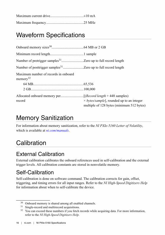
Waveform Specifications
............................................................................Onboard memory sizes30 64 MB or 2 GB
............................................................................Minimum record length 1 sample
............................................................................Number of pretrigger samples31 Zero up to full record length
............................................................................Number of posttrigger samples31 Zero up to full record length
Maximum number of records in onboardmemory32
....................................................................64 MB 65,536
....................................................................2 GB 100,000
............................................................................Allocated onboard memory perrecord
[(Record length + 448 samples)× bytes/sample], rounded up to an integermultiple of 128 bytes (minimum 512 bytes)
Memory SanitizationFor information about memory sanitization, refer to the NI PXIe-5160 Letter of Volatility,which is available at ni.com/manuals.
Calibration
External CalibrationExternal calibration calibrates the onboard references used in self-calibration and the externaltrigger levels. All calibration constants are stored in nonvolatile memory.
Self-CalibrationSelf-calibration is done on software command. The calibration corrects for gain, offset,triggering, and timing errors for all input ranges. Refer to the NI High-Speed Digitizers Helpfor information about when to self-calibrate the device.
30 Onboard memory is shared among all enabled channels.31 Single-record and multirecord acquisitions.32 You can exceed these numbers if you fetch records while acquiring data. For more information,
refer to the NI High-Speed Digitizers Help.
16 | ni.com | NI PXIe-5160 Specifications
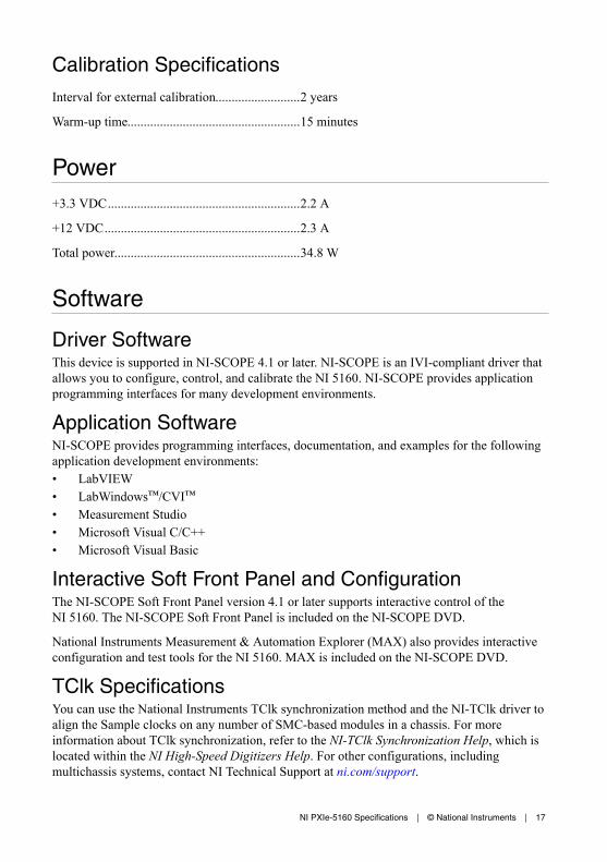
Calibration Specifications
............................................................................Interval for external calibration 2 years
............................................................................Warm-up time 15 minutes
Power............................................................................+3.3 VDC 2.2 A
............................................................................+12 VDC 2.3 A
............................................................................Total power 34.8 W
Software
Driver SoftwareThis device is supported in NI-SCOPE 4.1 or later. NI-SCOPE is an IVI-compliant driver thatallows you to configure, control, and calibrate the NI 5160. NI-SCOPE provides applicationprogramming interfaces for many development environments.
Application SoftwareNI-SCOPE provides programming interfaces, documentation, and examples for the followingapplication development environments:• LabVIEW• LabWindows™/CVI™
• Measurement Studio• Microsoft Visual C/C++• Microsoft Visual Basic
Interactive Soft Front Panel and ConfigurationThe NI-SCOPE Soft Front Panel version 4.1 or later supports interactive control of theNI 5160. The NI-SCOPE Soft Front Panel is included on the NI-SCOPE DVD.
National Instruments Measurement & Automation Explorer (MAX) also provides interactiveconfiguration and test tools for the NI 5160. MAX is included on the NI-SCOPE DVD.
TClk SpecificationsYou can use the National Instruments TClk synchronization method and the NI-TClk driver toalign the Sample clocks on any number of SMC-based modules in a chassis. For moreinformation about TClk synchronization, refer to the NI-TClk Synchronization Help, which islocated within the NI High-Speed Digitizers Help. For other configurations, includingmultichassis systems, contact NI Technical Support at ni.com/support.
NI PXIe-5160 Specifications | © National Instruments | 17
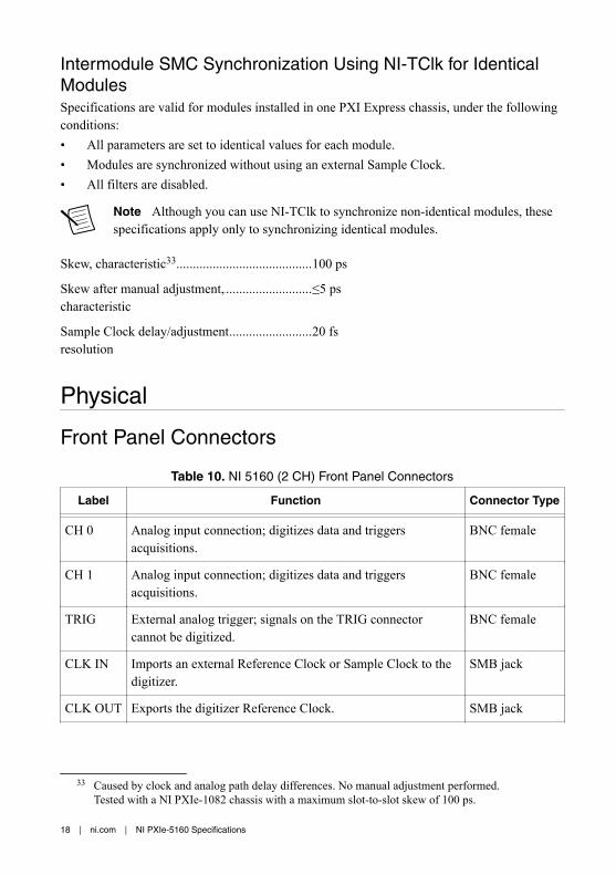
Intermodule SMC Synchronization Using NI-TClk for IdenticalModulesSpecifications are valid for modules installed in one PXI Express chassis, under the followingconditions:• All parameters are set to identical values for each module.• Modules are synchronized without using an external Sample Clock.• All filters are disabled.
Note Although you can use NI-TClk to synchronize non-identical modules, thesespecifications apply only to synchronizing identical modules.
............................................................................Skew, characteristic33 100 ps
............................................................................Skew after manual adjustment,characteristic
≤5 ps
............................................................................Sample Clock delay/adjustmentresolution
20 fs
Physical
Front Panel Connectors
Table 10. NI 5160 (2 CH) Front Panel Connectors
Label Function Connector Type
CH 0 Analog input connection; digitizes data and triggersacquisitions.
BNC female
CH 1 Analog input connection; digitizes data and triggersacquisitions.
BNC female
TRIG External analog trigger; signals on the TRIG connectorcannot be digitized.
BNC female
CLK IN Imports an external Reference Clock or Sample Clock to thedigitizer.
SMB jack
CLK OUT Exports the digitizer Reference Clock. SMB jack
33 Caused by clock and analog path delay differences. No manual adjustment performed.Tested with a NI PXIe-1082 chassis with a maximum slot-to-slot skew of 100 ps.
18 | ni.com | NI PXIe-5160 Specifications
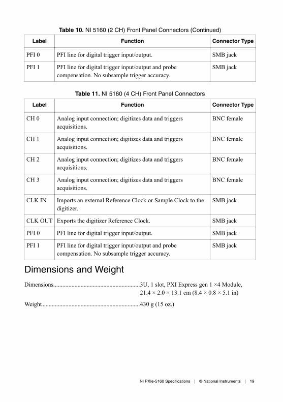
Table 10. NI 5160 (2 CH) Front Panel Connectors (Continued)
Label Function Connector Type
PFI 0 PFI line for digital trigger input/output. SMB jack
PFI 1 PFI line for digital trigger input/output and probecompensation. No subsample trigger accuracy.
SMB jack
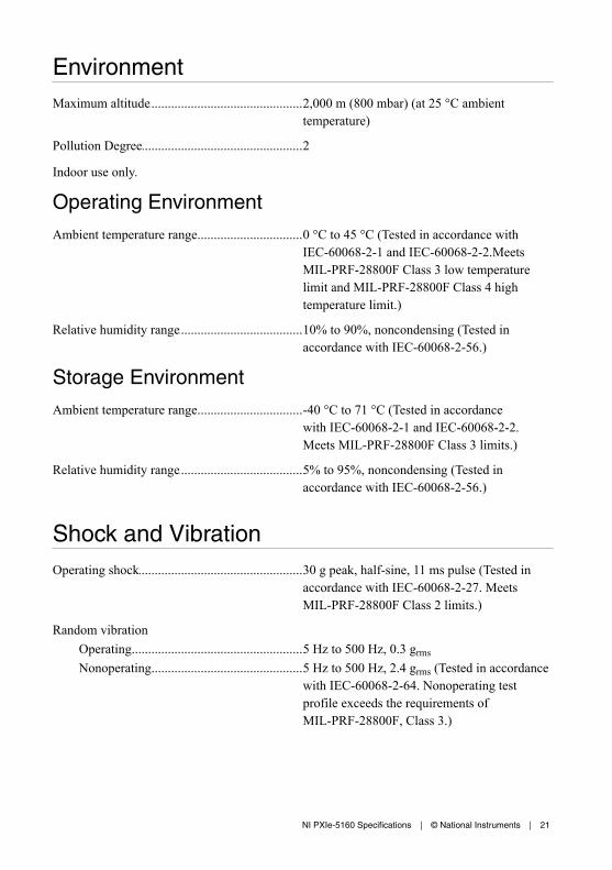
Table 11. NI 5160 (4 CH) Front Panel Connectors
Label Function Connector Type
CH 0 Analog input connection; digitizes data and triggersacquisitions.
BNC female
CH 1 Analog input connection; digitizes data and triggersacquisitions.
BNC female
CH 2 Analog input connection; digitizes data and triggersacquisitions.
BNC female
CH 3 Analog input connection; digitizes data and triggersacquisitions.
BNC female
CLK IN Imports an external Reference Clock or Sample Clock to thedigitizer.
SMB jack
CLK OUT Exports the digitizer Reference Clock. SMB jack
PFI 0 PFI line for digital trigger input/output. SMB jack
PFI 1 PFI line for digital trigger input/output and probecompensation. No subsample trigger accuracy.
SMB jack
Dimensions and Weight
............................................................................Dimensions 3U, 1 slot, PXI Express gen 1 ×4 Module,21.4 × 2.0 × 13.1 cm (8.4 × 0.8 × 5.1 in)
............................................................................Weight 430 g (15 oz.)
NI PXIe-5160 Specifications | © National Instruments | 19
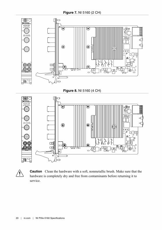
Figure 7. NI 5160 (2 CH)
NI PXIe-516010-Bit 2.5 GS/s
500 MHz Digitizer
50Ω: 5 Vpk MAX1MΩ: 42 Vpk MAX
CH 1
CH 0
TRIG
CLKIN
OUT 1
PFI0
Figure 8. NI 5160 (4 CH)
NI PXIe–516010-Bit 2.5 GS/s
500 MHz Digitizer
CH 0
CH 1
CH 2
50Ω: 5 Vpk MAX1MΩ: 42 Vpk MAX
CH 3
CLKIN
OUT 1
PFI0
Caution Clean the hardware with a soft, nonmetallic brush. Make sure that thehardware is completely dry and free from contaminants before returning it toservice.
20 | ni.com | NI PXIe-5160 Specifications
Environment............................................................................Maximum altitude 2,000 m (800 mbar) (at 25 °C ambient
temperature)
............................................................................Pollution Degree 2
Indoor use only.
Operating Environment
............................................................................Ambient temperature range 0 °C to 45 °C (Tested in accordance withIEC-60068-2-1 and IEC-60068-2-2.MeetsMIL-PRF-28800F Class 3 low temperaturelimit and MIL-PRF-28800F Class 4 hightemperature limit.)
............................................................................Relative humidity range 10% to 90%, noncondensing (Tested inaccordance with IEC-60068-2-56.)
Storage Environment
............................................................................Ambient temperature range -40 °C to 71 °C (Tested in accordancewith IEC-60068-2-1 and IEC-60068-2-2.Meets MIL-PRF-28800F Class 3 limits.)
............................................................................Relative humidity range 5% to 95%, noncondensing (Tested inaccordance with IEC-60068-2-56.)
Shock and Vibration............................................................................Operating shock 30 g peak, half-sine, 11 ms pulse (Tested in
accordance with IEC-60068-2-27. MeetsMIL-PRF-28800F Class 2 limits.)
Random vibration....................................................................Operating 5 Hz to 500 Hz, 0.3 grms
....................................................................Nonoperating 5 Hz to 500 Hz, 2.4 grms (Tested in accordancewith IEC-60068-2-64. Nonoperating testprofile exceeds the requirements ofMIL-PRF-28800F, Class 3.)
NI PXIe-5160 Specifications | © National Instruments | 21
Compliance and Certifications
SafetyThis product is designed to meet the requirements of the following electrical equipment safetystandards for measurement, control, and laboratory use:• IEC 61010-1, EN 61010-1• UL 61010-1, CSA 61010-1
Note For UL and other safety certifications, refer to the product label or the OnlineProduct Certification section.
Electromagnetic CompatibilityThis product meets the requirements of the following EMC standards for electrical equipmentfor measurement, control, and laboratory use:• EN 61326-1 (IEC 61326-1): Class A emissions; Basic immunity• EN 55011 (CISPR 11): Group 1, Class A emissions• AS/NZS CISPR 11: Group 1, Class A emissions• FCC 47 CFR Part 15B: Class A emissions• ICES-001: Class A emissions
Note In the United States (per FCC 47 CFR), Class A equipment is intended foruse in commercial, light-industrial, and heavy-industrial locations. In Europe,Canada, Australia, and New Zealand (per CISPR 11), Class A equipment is intendedfor use only in heavy-industrial locations.
Note Group 1 equipment (per CISPR 11) is any industrial, scientific, or medicalequipment that does not intentionally generate radio frequency energy for thetreatment of material or inspection/analysis purposes.
Note For EMC declarations and certifications, refer to the Online ProductCertification section.
CE Compliance This product meets the essential requirements of applicable European Directives, as amendedfor CE marking, as follows:• 2006/95/EC; Low-Voltage Directive (safety)• 2004/108/EC; Electromagnetic Compatibility Directive (EMC)
Online Product CertificationTo obtain product certifications and the DoC for this product, visit ni.com/certification, searchby model number or product line, and click the appropriate link in the Certification column.
22 | ni.com | NI PXIe-5160 Specifications
Environmental ManagementNI is committed to designing and manufacturing products in an environmentally responsiblemanner. NI recognizes that eliminating certain hazardous substances from our products isbeneficial not only to the environment but also to NI customers.
For additional environmental information, refer to the Minimize Our Environmental Impactweb page at ni.com/environment. This page contains the environmental regulations anddirectives with which NI complies, as well as other environmental information not included inthis document.
Waste Electrical and Electronic Equipment (WEEE)EU Customers At the end of the product life cycle, all products must be sent to aWEEE recycling center. For more information about WEEE recycling centers,National Instruments WEEE initiatives, and compliance withWEEE Directive 2002/96/EC on Waste Electrical and Electronic Equipment, visit ni.com/environment/weee.htm.
电子信息产品污染控制管理办法(中国 RoHS)中国客户 National Instruments 符合中国电子信息产品中限制使用某些有害物
质指令(RoHS)。关于 National Instruments 中国 RoHS 合规性信息,请登录
ni.com/environment/rohs_china。(For information about China RoHScompliance, go to ni.com/environment/rohs_china.)
NI PXIe-5160 Specifications | © National Instruments | 23

Refer to the NI Trademarks and Logo Guidelines at ni.com/trademarks for information on National Instruments trademarks.Other product and company names mentioned herein are trademarks or trade names of their respective companies. For patentscovering National Instruments products/technology, refer to the appropriate location: Help»Patents in your software, thepatents.txt file on your media, or the National Instruments Patent Notice at ni.com/patents. You can find information aboutend-user license agreements (EULAs) and third-party legal notices in the readme file for your NI product. Refer to the ExportCompliance Information at ni.com/legal/export-compliance for the National Instruments global trade compliance policy andhow to obtain relevant HTS codes, ECCNs, and other import/export data.
© 2013—2014 National Instruments. All rights reserved.
374020C-01 Apr14