NHD-3.5-320240MF-ATXL#-CTP-1 · 8 7/20/18 CTP Adhesive Increased from 0.18 to 0.3mm, & Backlight...
16
NHD-3.5-320240MF-ATXL#-CTP-1 TFT (Thin-Film-Transistor) Color Liquid Crystal Display Module NHD- Newhaven Display 3.5- 3.5” Diagonal 320240- 320xRGBx240 Pixels MF- Model A- Built-in Driver / No Controller T- White LED Backlight X- TFT L- 12:00 Optimal View, Wide Temperature #- RoHS Compliant CTP-1 Capacitive Touch Panel with Controller Newhaven Display International, Inc. 2661 Galvin Ct. Elgin IL, 60124 Ph: 847-844-8795 Fax: 847-844-8796 www.newhavendisplay.com [email protected] [email protected]
Transcript of NHD-3.5-320240MF-ATXL#-CTP-1 · 8 7/20/18 CTP Adhesive Increased from 0.18 to 0.3mm, & Backlight...

NHD-3.5-320240MF-ATXL#-CTP-1
TFT (Thin-Film-Transistor) Color Liquid Crystal Display Module
NHD- Newhaven Display 3.5- 3.5” Diagonal 320240- 320xRGBx240 Pixels MF- Model A- Built-in Driver / No Controller T- White LED Backlight X- TFT L- 12:00 Optimal View, Wide Temperature #- RoHS Compliant CTP-1 Capacitive Touch Panel with Controller
Newhaven Display International, Inc.
2661 Galvin Ct. Elgin IL, 60124
Ph: 847-844-8795 Fax: 847-844-8796
www.newhavendisplay.com [email protected] [email protected]

[2]
Document Revision History Revision Date Description Changed by
0 2/1/2012 Initial Release SB
1 12/11/2012 Timing characteristics updated AK
2 4/25/2014 Optical characteristics updated ML
3 5/30/2014 Driver information updated AK
4 4/1/2015 CTP mechanical dimensions updated AK
5 12/03/15 Luminance Updated, Backlight Lifetime Added, Datasheet Reformat
SB
6 7/5/16 Chromaticity Added SB
7 12/8/16 VDD, IDD, and Chromaticity Updated SB
8 7/20/18 CTP Adhesive Increased from 0.18 to 0.3mm, & Backlight Characteristics Updated
SB
Functions and Features • 320xRGBx240 resolution
• LED backlight
• 3.3V power supply
• 24-bit Parallel digital RGB interface (6.4MHz)
• Capacitive Touch Panel with controller o 5 point multi-touch input o Gesture input
▪ Zoom In/Out ▪ Swipe Up/Down/Left/Right

C
B
A
D
E
F
C
B
A
D
E
F
4321 8765
4321 8765
CHECKED BY:
DRAWN DATE:
07/20/18 NSSHEET 1 OF 1
- THIRD ANGLE PROJECTION
DRAWING/PART NUMBER:
STANDARD TOLERANCES(UNLESS OTHERWISE SPECIFIED)
LINEAR:XX.XX.XXX.XX
UNLESS OTHERWISE SPECIFIED
NHD-3.5-320240MF-ATXL#-CTP-1REVISION:
1.0SIZE:
A3SCALE:
DRAWN BY:
S. BaxiCHECKED DATE:
THIS DRAWING IS SOLELY THE PROPERTY OF NEWHAVEN DISPLAY INTERNATIONAL, INC.THE INFORMATION IT CONTAINS IS NOT TO BE DISCLOSED, REPRODUCED OR COPIED INWHOLE OR PART WITHOUT WRITTEN APPROVAL FROM NEWHAVEN DISPLAY.
±0.3 mm±0.3 mm±0.3 mm
- DIMENSIONS ARE IN MILLIMETERS
SYMBOL REVISION DATE
DO NOT SCALE DRAWING
A. Khan
07/20/18
APPROVED BY:
APPROVED DATE:
07/20/18
A. Khan
NOTES:1. Display Size: 3.5” TFT2. Optimal View: Full View3. Display Mode: Transmissive / Normally White / Anti-Glare4. Driver IC: NV3035C5. Supply Voltage: 3.3V6. Backlight: White LED / 19.2 V (Typ) / 18 mA7. Brightness: 330 cd/m² (Typ)8. Touch Panel: PCAP
Symbol
Pin No. Symbol 1 LED_K 2 LED_K 3 LED_A 4 LED_A 5 NC 6 NC 7 NC 8 RSTB 9 SPENB
10 SPCK 11 SPDA
12-19 B0-B7 20-27 G0-G7 28-35 R0-R7
36 HSD 37 VSD 38 CLKIN 39 NC 40 NC 41 VDD 42 VDD 43 NC 44 NC 45 NC 46 NC 47 NC 48 NC 49 NC 50 NC 51 NC 52 DEN 53 GND 54 GND
76.90 ±0.170.68±0.15 (VA) 3.11
63.9
0 ±
0.1
53.1
6 ±
0.1
(VA)
7.92
4-R0.30
50.0
0±0.
5
16.0
0±0.
5 23.00±0.53.
6±0.
3
7.00±0.1
6.50
12.50
10.0
0
0.15
±0.1
2.7±
0.3
6*0.7±0.05
1.00±0.05(Pitch)
2-1.00±0.1
A0.3±0.05
CTP: 1.40Adhesive (0.3)
Total: 4.9±0.3
TFT: 3.2±0.15

[4]
Pin Description
TFT: Pin No. Symbol External Connection Function Description
1-2 LED_K Power Supply Backlight Cathode (Ground)
3-4 LED_A Power Supply Backlight Anode (18mA @ 19.2V)
5-7 NC - No Connect
8 RSTB MPU Active LOW Reset signal
9 SPENB MPU Active LOW Serial Chip Select signal
10 SPCK MPU Serial Clock signal
11 SPDA MPU Serial Data signal
12-19 B0-B7 MPU Blue Data signals
20-27 G0-G7 MPU Green Data signals
28-35 R0-R7 MPU Red Data signals
36 HSD MPU Horizontal (Line) Sync signal
37 VSD MPU Vertical (Frame) Sync signal
38 CLKIN MPU Dot Clock signal
39-40 NC - No Connect
41-42 VDD Power Supply Supply Voltage for LCD and logic (3.3V)
43-51 NC - No Connect
52 DEN - Data Enable signal (No Connect)
53-54 GND Power Supply Ground
Recommended connector: 54pin, 0.5mm pitch, FFC connector. Molex P/N 51296-5494
Capacitive Touch Panel: Pin No. Symbol External Connection Function Description
1 VDD Power Supply Supply voltage for Logic (3.0V)
2 VSS Power Supply Ground
3 SCL MPU Serial I2C Clock (Requires pull-up resistor)
4 SDA MPU Serial I2C Data (Requires pull-up resistor)
5 /INT MPU Interrupt signal from touch panel module to host
6 /RESET MPU Active LOW Reset signal
Recommended connector: 6pin, 1.0mm pitch, FFC connector. Molex P/N 52271-0679
Driver/Controller Information
TFT: Built-in NV3035C driver. No controller. Please download specification at http://www.newhavendisplay.com/app_notes/NV3035C.pdf Note: To achieve optimum VCOM and VGL settings, the SPI interface may be used to set the following registers: R0Eh = 6Bh R0Fh = 24h
Capacitive Touch Panel: Built-in FocalTech FT5216 Capacitive Touch Controller. Please download specification at http://www.newhavendisplay.com/app_notes/FT5x16.pdf

[5]
Electrical Characteristics
TFT: Item Symbol Condition Min. Typ. Max. Unit
Operating Temperature Range TOP Absolute Max -20 - +70 ⁰C
Storage Temperature Range TST Absolute Max -30 - +80 ⁰C
Supply Voltage VDD - 3.0 3.3 3.6 V
Supply Current IDD VDD=3.3V 5 10 20 mA
“H” Level input VIH - 0.8*VDD - VDD V
“L” Level input VIL - VSS - 0.2*VDD V
“H” Level output VOH - VDD-0.4 - VDD V
“L” Level output VOL - VSS - VSS+0.4 V
Backlight Supply Current ILED - - 18 20 mA
Backlight Supply Voltage VLED ILED = 18 mA 18.0 19.2 20.4 V
Backlight Lifetime* - ILED = 18 mA TOP = 25° C
20,000 50,000 - Hrs.
*Backlight lifetime is rated as Hours until half-brightness, under normal operating conditions. The LED of the backlight is driven by current drain; drive voltage is for reference only. Drive voltage must be selected to ensure backlight current drain is below MAX level stated.
Capacitive Touch Panel: Item Symbol Condition Min. Typ. Max. Unit
Operating Temperature Range TOP Absolute Max -20 - +70 ⁰C
Storage Temperature Range TST Absolute Max -30 - +80 ⁰C
Supply Voltage VDD - 2.8 3.3 3.6 V
Supply Current – Operating IDD VDD = 3.3V
- 6.0 - mA
Supply Current – Hibernate IDD - 1.0 - µA
“H” Level input VIH - 0.7*VDD - VDD V
“L” Level input VIL - VSS - 0.3*VDD V
“H” Level output VOH - 0.7*VDD - VDD V
“L” Level output VOL - VSS - 0.3*VDD V
Optical Characteristics Item Symbol Condition Min. Typ. Max. Unit
Optimal Viewing Angles
Top ϕY+
CR ≥ 10
- 60 - ⁰
Bottom ϕY- - 40 - ⁰
Left θX- - 60 - ⁰
Right θX+ - 60 - ⁰
Contrast Ratio CR - 200 350 - -
Luminance LV ILED = 18mA 265 330 - cd/m2
Response Time Rise TR
TOP=25°C - 25 40 ms
Fall TF - 25 40 ms
Chromaticity
Red XR - 0.556 0.606 0.656 -
YR - 0.302 0.352 0.402 -
Green XG - 0.268 0.318 0.368 -
YG - 0.541 0.591 0.641 -
Blue XB - 0.093 0.143 0.193 -
YG - 0.052 0.102 0.152 -
White XW - 0.230 0.280 0.330 -
YW - 0.256 0.306 0.356 -

[6]
Capacitive Touch Panel Material Characteristics: Property Requirement Unit
IC FT5216GM7 -
ITO Glass thickness 0.55 mm
Surface Hardness ≥6 H
Light transmission 83% ± 5% -
Operating Humidity 20~90 RH
Storage Humidity 20~90 RH
Capacitive Touch Panel Registers Address Name B7 B6 B5 B4 B3 B2 B1 B0 Access
00h DEVICE_MODE
Device Mode [2..0]
R/W
01h GEST_ID Gesture ID [7..0] R
02h TD_STATUS
Touch Points [3..0] R
03h TOUCH1_XH Event Flag
1st Touch X Position MSB [11..8] R
04h TOUCH1_XL 1st Touch X Position LSB [7..0] R
05h TOUCH1_YH Touch ID [3..0] 1st Touch Y Position MSB [11..8] R
06h TOUCH1_YL 1st Touch Y Position LSB [7..0] R
07h
R
08h
R
09h TOUCH2_XH Event Flag
2nd Touch X Position MSB [11..8] R
0Ah TOUCH2_XL 2nd Touch X Position LSB [7..0] R
0Bh TOUCH2_YH Touch ID [3..0] 2nd Touch Y Position MSB [11..8] R
0Ch TOUCH2_YL 2nd Touch Y Position LSB [7..0] R
0Dh
R
0Eh
R
0Fh TOUCH3_XH Event Flag
3rd Touch X Position MSB [11..8] R
10h TOUCH3_XL 3rd Touch X Position LSB [7..0] R
11h TOUCH3_YH Touch ID [3..0] 3rd Touch Y Position MSB [11..8] R
12h TOUCH3_YL 3rd Touch Y Position LSB [7..0] R
13h
R
14h
R
15h TOUCH4_XH Event Flag
4th Touch X Position MSB [11..8] R
16h TOUCH4_XL 4th Touch X Position LSB [7..0] R
17h TOUCH4_YH Touch ID [3..0] 4th Touch Y Position MSB [11..8] R
18h TOUCH4_YL 4th Touch Y Position LSB [7..0] R
19h
R
1Ah
R
1Bh TOUCH5_XH Event Flag
5th Touch X Position MSB [11..8] R
1Ch TOUCH5_XL 5th Touch X Position LSB [7..0] R
1Dh TOUCH5_YH Touch ID [3..0] 5th Touch Y Position MSB [11..8] R
1Eh TOUCH5_YL 5th Touch Y Position LSB [7..0] R
1Fh
R

[7]
Address Name B7 B6 B5 B4 B3 B2 B1 B0 Access
80h ID_G_THGROUP valid touching detect threshold R/W
81h ID_G_THPEAK valid touching peak detect threshold R/W
82h ID_G_THCAL the threshold when calculating the focus of touching R/W
83h ID_G_THWATER the threshold when there is surface water R/W
84h ID_G_TEMP the threshold of temperature compensation R/W
85h ID_G_THDIFF the threshold whether the coordinate is different from original R/W
86h ID_G_CTRL
Power Control Mode [1..0] R/W
87h ID_G_TIME_ENTER_MONITOR the timer for entering monitor status R/W
88h ID_G_PERIODACTIVE
Period Active [3..0] R/W
89h ID_G_PERIODMONITOR the timer of entering idle when in monitor status R/W
A0h ID_G_AUTO_CLB_MODE auto calibration mode R/W
A1h ID_G_LIB_VERSION_H Firmware Library Version H byte R
A2h ID_G_LIB_VERSION_L Firmware Library Version L byte R
A3h ID_G_CIPHER Chip vendor ID R
A4h ID_G_MODE the interrupt status to host R
A5h ID_G_PMODE Power Consume Mode A6h ID_G_FIRMID Firmware ID R
A7h ID_G_STATE Running State A8h ID_G_FT5201ID CTPM Vendor ID R
A9h ID_G_ERR Error Code R
AAh ID_G_CLB Configure TP module during calibration in Test Mode R/W
FEh LOG_MSG_CNT The log MSG count R
FFh LOG_CUR_CHA Current character of log message R
NOTE: Registers 80h – AFh have been configured for optimum settings and do not need to be modified.

[8]
Register No Register Name Bits Value Description
00h Device Mode [2:0] 000b Normal Operating Mode
100b Test Mode - read raw data (reserved)
001b System Information Mode (reserved)
01h Gesture ID [7:0] 48h Zoom In
49h Zoom Out
00h No Gesture
02h Touch Points [3:0] 000b 0 touch points detected
001b 1 touch point detected
010b 2 touch points detected
011b 3 touch points detected
100b 4 touch points detected
101b 5 touch points detected
03h Touch 1 Event Flag [7:6] 00b Put Down
01b Put Up
10b Contact
11b Reserved
03h TOUCH1_XH [3:0] 0h - 1h Upper 4 bits of X touch coordinate
04h TOUCH1_XL [7:0] 00h - FFh Lower 8 bits of X touch coordinate
05h TOUCH1_YH [3:0] 0h - 1h Upper 4 bits of Y touch coordinate
06h TOUCH1_YL [7:0] 00h - FFh Lower 8 bits of Y touch coordinate
09h Touch 2 Event Flag [7:6] 00b Put Down
01b Put Up
10b Contact
11b Reserved
09h TOUCH2_XH [3:0] 0h - 1h Upper 4 bits of X touch coordinate
0Ah TOUCH2_XL [7:0] 00h - FFh Lower 8 bits of X touch coordinate
0Bh TOUCH2_YH [3:0] 0h - 1h Upper 4 bits of Y touch coordinate
0Ch TOUCH2_YL [7:0] 00h - FFh Lower 8 bits of Y touch coordinate
0Fh Touch 3 Event Flag [7:6] 00b Put Down
01b Put Up
10b Contact
11b Reserved
0Fh TOUCH3_XH [3:0] 0h - 1h Upper 4 bits of X touch coordinate
10h TOUCH3_XL [7:0] 00h - FFh Lower 8 bits of X touch coordinate
11h TOUCH3_YH [3:0] 0h - 1h Upper 4 bits of Y touch coordinate
12h TOUCH3_YL [7:0] 00h - FFh Lower 8 bits of Y touch coordinate
15h Touch 4 Event Flag [7:6] 00b Put Down
01b Put Up
10b Contact
11b Reserved
15h TOUCH4_XH [3:0] 0h - 1h Upper 4 bits of X touch coordinate
16h TOUCH4_XL [7:0] 00h - FFh Lower 8 bits of X touch coordinate
17h TOUCH4_YH [3:0] 0h - 1h Upper 4 bits of Y touch coordinate
18h TOUCH4_YL [7:0] 00h - FFh Lower 8 bits of Y touch coordinate

[9]
Register No Register Name Bits Value Description
1Bh Touch 5 Event Flag [7:6] 00b Put Down
01b Put Up
10b Contact
11b Reserved
1Bh TOUCH5_XH [3:0] 0h - 1h Upper 4 bits of X touch coordinate
1Ch TOUCH5_XL [7:0] 00h - FFh Lower 8 bits of X touch coordinate
1Dh TOUCH5_YH [3:0] 0h - 1h Upper 4 bits of Y touch coordinate
1Eh TOUCH5_YL [7:0] 00h - FFh Lower 8 bits of Y touch coordinate
80h ID_G_THGROUP [7:0] 00h - FFh Valid touching detect threshold Recommended: 46h
Actual value will be 4 times register’s value
81h ID_G_THPEAK [7:0] 00h - FFh valid touching peak detect threshold Recommended: 3Ch
82h ID_G_THCAL [7:0] 00h - FFh Touch focus threshold Recommended: 1Dh
83h ID_G_THWATER [7:0] 00h - FFh threshold when there is surface water Recommended: D3h
84h ID_G_THTEMP [7:0] 00h- FFh threshold of temperature compensation Recommended: EBh
85h ID_G_THDIFF [7:0] 00h- FFh Touch difference threshold Recommended: A0h
Actual value is 32 times the register’s value
86h ID_G_CTRL [1:0] 00h Power Control Mode: Not Auto Jump
01h Power Control Mode: Auto Jump
87h ID_G_TIME_ENTER_MONITOR [7:0] 00h-FFh Delay to enter 'Monitor' status (s) Recommended: C8h
88h ID_G_PERIODACTIVE [3:0] 3h-Eh Period of 'Active' status (ms) Recommended: 6h
89h ID_G_PERIODMONITOR [7:0] 1Eh-FFh Timer to enter ‘idle’ when in 'Monitor' (ms) Recommended: 28h
A0h ID_G_AUTO_CLB_MODE [7:0] 00h Auto calibration mode: Enable auto calibration
FFh Auto calibration mode: Disable auto calibration
A1h ID_G_LIB_VERSION_H [7:0] 30h Firmware Library Version H byte
A2h ID_G_LIB_VERSION_L [7:0] 01h Firmware Library Version L byte
A3h ID_G_CIPHER [7:0] 0Ah Chip vendor ID
A4h ID_G_MODE [0:0] 00h Interrupt status: Enable interrupt to host
01h Interrupt status: Disable interrupt to host
A5h ID_G_PMODE [1:0] 00h 'Active' Mode
01h 'Monitor' Mode
03h 'Hibernate' Mode
A6h ID_G_FIRMID [7:0] 06h Firmware ID
A7h ID_G_STATE [7:0] 00h Running State: Configure
01h Running State: Work
02h Running State: Calibration
03h Running State: Factory
04h Running State: Auto-calibration
A8h ID_G_FT5201ID [7:0] 79h CTPM Vendor's Chip ID
A9h ID_G_ERR [7:0] 01h Error Code: OK
03h Error Code: Chip register writing inconsistent with reading
05h Error Code: Chip start fail
1Ah Error Code: Calibration match fail

[10]
Timing Characteristics – TFT Display

[11]
Input Data Format
Clock and Data Input Timing Diagram

[12]
3-wire Timing Diagram
Input Data Timing

[13]
Timing Characteristics – Capacitive Touch Panel Data Transfer Format

[14]
Power ON Sequence
Reset Sequence

[15]
Sample code to read touch data:
i2c_start(); i2c_tx(0x70); //Slave Address (Write) i2c_tx(0x00); //Start reading address i2c_stop();
i2c_start(); i2c_tx(0x71); //Slave Address (Read) for(i=0x00;i<0x1F;i++) {touchdata_buffer[i] = i2c_rx(1);} i2c_stop();
Sample code to overwrite default register values:
i2c_start(); i2c_tx(0x70); //Slave Address (Write) i2c_tx(0xA4); //ID_G_Mode i2c_tx(0x01); //Disable interrupt status to host i2c_stop();
[16]
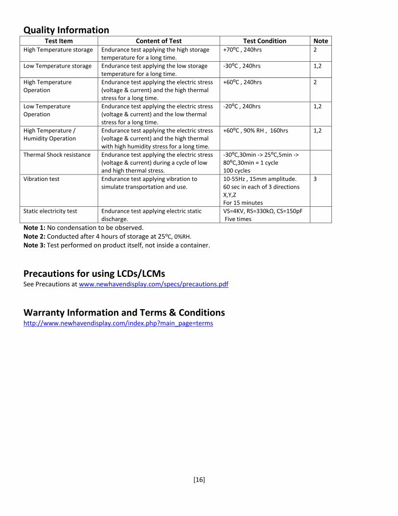
Quality Information Test Item Content of Test Test Condition Note
High Temperature storage Endurance test applying the high storage temperature for a long time.
+70⁰C , 240hrs 2
Low Temperature storage Endurance test applying the low storage temperature for a long time.
-30⁰C , 240hrs 1,2
High Temperature Operation
Endurance test applying the electric stress (voltage & current) and the high thermal stress for a long time.
+60⁰C , 240hrs 2
Low Temperature Operation
Endurance test applying the electric stress (voltage & current) and the low thermal stress for a long time.
-20⁰C , 240hrs 1,2
High Temperature / Humidity Operation
Endurance test applying the electric stress (voltage & current) and the high thermal with high humidity stress for a long time.
+60⁰C , 90% RH , 160hrs 1,2
Thermal Shock resistance Endurance test applying the electric stress (voltage & current) during a cycle of low and high thermal stress.
-30⁰C,30min -> 25⁰C,5min -> 80⁰C,30min = 1 cycle 100 cycles
Vibration test Endurance test applying vibration to simulate transportation and use.
10-55Hz , 15mm amplitude. 60 sec in each of 3 directions X,Y,Z For 15 minutes
3
Static electricity test Endurance test applying electric static discharge.
VS=4KV, RS=330kΩ, CS=150pF Five times
Note 1: No condensation to be observed. Note 2: Conducted after 4 hours of storage at 25⁰C, 0%RH.
Note 3: Test performed on product itself, not inside a container.
Precautions for using LCDs/LCMs See Precautions at www.newhavendisplay.com/specs/precautions.pdf
Warranty Information and Terms & Conditions http://www.newhavendisplay.com/index.php?main_page=terms