Next Generation Microprocessor Status, Use Cases and ...
38
Next Generation Microprocessor Status, Use Cases and Benchmarks ESA Workshop in Avionics Data, Control and Software Systems (ADCSS) 2011 Multi-Core Processors for Space Applications 27 October, 2011 www.aeroflex.com/gaisler
Transcript of Next Generation Microprocessor Status, Use Cases and ...

Next Generation Microprocessor
Status, Use Cases and Benchmarks
ESA Workshop in Avionics Data, Controland Software Systems (ADCSS) 2011Multi-Core Processors for Space Applications
27 October, 2011
www.aeroflex.com/gaisler

2
Overview
• NGMP is an ESA activity developing a multi-core system with higher performance compared to earlier generations of European Space processors
• Part of the ESA roadmap for standard microprocessor components
• Aeroflex Gaisler's assignment consists of specification, the architectural (VHDL) design, and verification by simulation and on FPGA
• FPGA prototypes with several downsized configurations have been delivered.
• NGMP activity is currently on hold in anticipation of progress on the European Space DSM technology. To be resumed in 2012.
• Work is progressing on developing a functional prototype (FP)
• This presentation will focus on: Current status, architecture overview, how to use the NGMP and some preliminary benchmark data

3
Current status / Development Schedule
• NGMP activity
– Aug 2009: Kick-off
– Feb 2010: Definition and specification
– June 2010: First versions of FPGA prototypes
– Dec 2010: Final RTL code, FPGA Demonstrator
– Aug 2011: Verified ASIC netlist (postponed)
• Functional prototype
– May 2011: Kick-off
– July 2011: Definition and specification
– Nov 2011: Architectural/Detailed design
– Jan 2012: Layout generation and verification
– May 2012: Prototype implementation, design validation
– Devices on evaluation board are expected to be available in Q2 2012.
• Manufacturing of FM prototype parts not yet decided
• Development of flight model in a separate contract
4
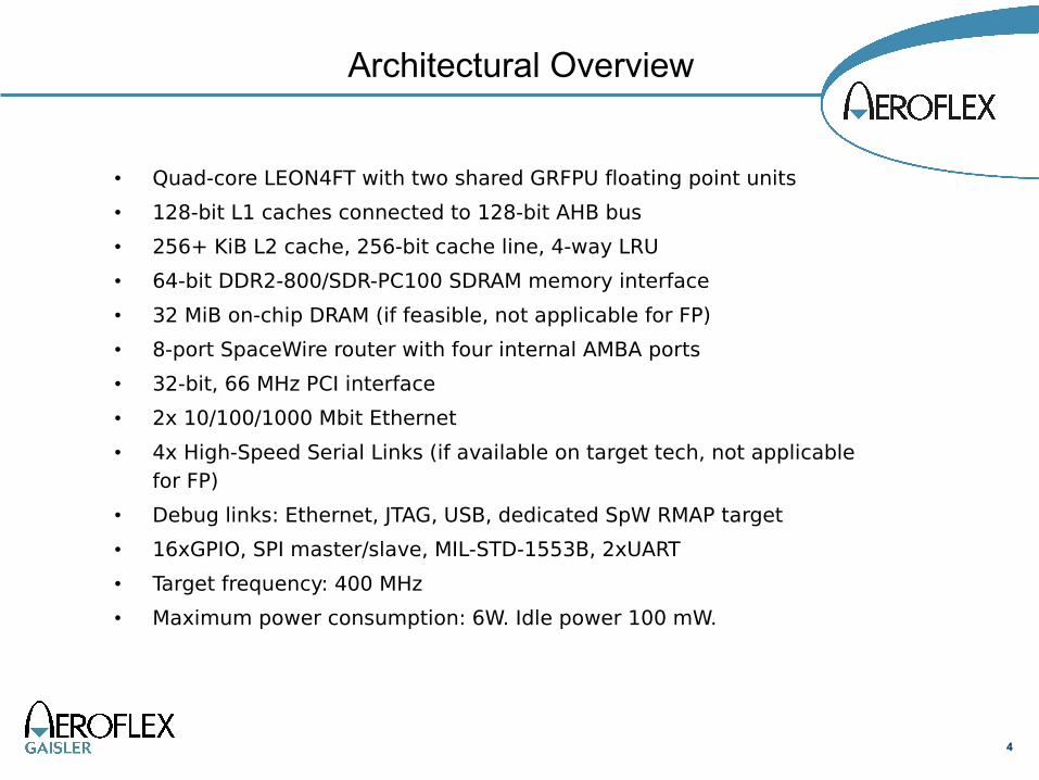
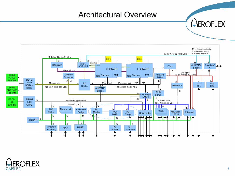
Architectural Overview
• Quad-core LEON4FT with two shared GRFPU floating point units
• 128-bit L1 caches connected to 128-bit AHB bus
• 256+ KiB L2 cache, 256-bit cache line, 4-way LRU
• 64-bit DDR2-800/SDR-PC100 SDRAM memory interface
• 32 MiB on-chip DRAM (if feasible, not applicable for FP)
• 8-port SpaceWire router with four internal AMBA ports
• 32-bit, 66 MHz PCI interface
• 2x 10/100/1000 Mbit Ethernet
• 4x High-Speed Serial Links (if available on target tech, not applicable for FP)
• Debug links: Ethernet, JTAG, USB, dedicated SpW RMAP target
• 16xGPIO, SPI master/slave, MIL-STD-1553B, 2xUART
• Target frequency: 400 MHz
• Maximum power consumption: 6W. Idle power 100 mW.
5
Architectural Overview
L2Cache
PCIMaster
128-bit AHB @ 400 MHz
32-bit AHB @ 400 MHz
Processor bus
Slave IO bus
PROM& IO
CTRL
PROMIO
8/16-bit
HSSLSpW router
USBDCL
MemoryScrubber
128-bit AHB @ 400 MHz
Memory bus
UARTGPIO
DSU
AHBStatus
JTAGDCL
AHB/APBBridge
AHB/AHBBridge
PCITarget
PCIDMA
Ethernet
AHB BridgeIOMMU
AHB/AHBBridge
32-bit AHB @ 400 MHz
Master IO bus
32-bit AHB @ 400 MHzDebug bus
32-bit APB @ 400 MHz
SpW RMAPDCL
AHBStatus
PCIArbiter
EthernetHSSLHSSLHSSL
UART
S S SS S S
SS
S
S
S
SM
SMM
M
M MM
MMM
M
MS
S
S S S
M = Master interface(s)S = Slave interface(s)X = Snoop interface
X
X
MX
S
X
M
SM
S
S
MX
IRQ(A)MP
Timers 0watchdog
S
S
MX MX
CLKGATE S
AHBTRACE
AHB/APBBridge
32-bit APB @ 400 MHz
LEON4STAT. UNIT
S
M
M SS
Timers 1 -4 S
X
S
M
Statistics
Interrupt bus
Caches MMU
FPU
FPU
Caches MMU
IRQCTRL
LEON4FTCaches MMU
LEON4FT
FPU
FPUIRQCTRL
LEON4FTCaches MMU
LEON4FT
S
SPIcontroller
S
96-bitDDR2-800SDRAM
96-bitPC100
SDRAM DDR2AND
SDRAMCTRL
MIL-STD-1553B
M
S

6
Architecture - Processor Bus
L2Cache
PCIMaster
128-bit AHB @ 400 MHz
32-bit AHB @ 400 MHz
Processor bus
Slave IO bus
PROM& IO
CTRL
PROMIO
8/16-bit
HSSLSpW router
USBDCL
MemoryScrubber
128-bit AHB @ 400 MHz
Memory bus
UARTGPIO
DSU
AHBStatus
JTAGDCL
AHB/APBBridge
AHB/AHBBridge
PCITarget
PCIDMA
Ethernet
AHB BridgeIOMMU
AHB/AHBBridge
32-bit AHB @ 400 MHz
Master IO bus
32-bit AHB @ 400 MHzDebug bus
32-bit APB @ 400 MHz
SpW RMAPDCL
AHBStatus
PCIArbiter
EthernetHSSLHSSLHSSL
UART
S S SS S S
SS
S
S
S
SM
SMM
M
M MM
MMM
M
MS
S
S S S
M = Master interface(s)S = Slave interface(s)X = Snoop interface
X
X
MX
S
X
M
SM
S
S
MX
IRQ(A)MP
Timers 0watchdog
S
S
MX MX
CLKGATE S
AHBTRACE
AHB/APBBridge
32-bit APB @ 400 MHz
LEON4STAT. UNIT
S
M
M SS
Timers 1 -4 S
X
S
M
Statistics
Interrupt bus
Caches MMU
FPU
FPU
Caches MMU
IRQCTRL
LEON4FTCaches MMU
LEON4FT
FPU
FPUIRQCTRL
LEON4FTCaches MMU
LEON4FT
S
SPIcontroller
S
96-bitDDR2-800SDRAM
96-bitPC100
SDRAM DDR2AND
SDRAMCTRL
MIL-STD-1553B
M
S
7
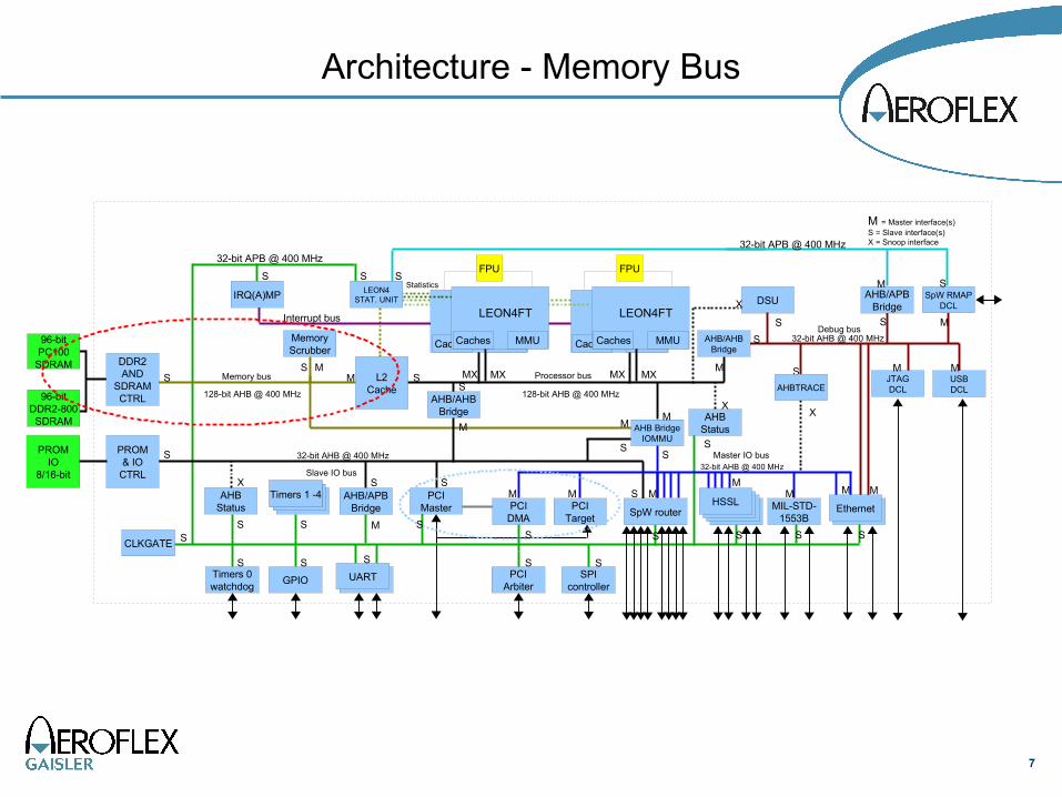
Architecture - Memory Bus
L2Cache
PCIMaster
128-bit AHB @ 400 MHz
32-bit AHB @ 400 MHz
Processor bus
Slave IO bus
PROM& IO
CTRL
PROMIO
8/16-bit
HSSLSpW router
USBDCL
MemoryScrubber
128-bit AHB @ 400 MHz
Memory bus
UARTGPIO
DSU
AHBStatus
JTAGDCL
AHB/APBBridge
AHB/AHBBridge
PCITarget
PCIDMA
Ethernet
AHB BridgeIOMMU
AHB/AHBBridge
32-bit AHB @ 400 MHz
Master IO bus
32-bit AHB @ 400 MHzDebug bus
32-bit APB @ 400 MHz
SpW RMAPDCL
AHBStatus
PCIArbiter
EthernetHSSLHSSLHSSL
UART
S S SS S S
SS
S
S
S
SM
SMM
M
M MM
MMM
M
MS
S
S S S
M = Master interface(s)S = Slave interface(s)X = Snoop interface
X
X
MX
S
X
M
SM
S
S
MX
IRQ(A)MP
Timers 0watchdog
S
S
MX MX
CLKGATE S
AHBTRACE
AHB/APBBridge
32-bit APB @ 400 MHz
LEON4STAT. UNIT
S
M
M SS
Timers 1 -4 S
X
S
M
Statistics
Interrupt bus
Caches MMU
FPU
FPU
Caches MMU
IRQCTRL
LEON4FTCaches MMU
LEON4FT
FPU
FPUIRQCTRL
LEON4FTCaches MMU
LEON4FT
S
SPIcontroller
S
96-bitDDR2-800SDRAM
96-bitPC100
SDRAM DDR2AND
SDRAMCTRL
MIL-STD-1553B
M
S
8
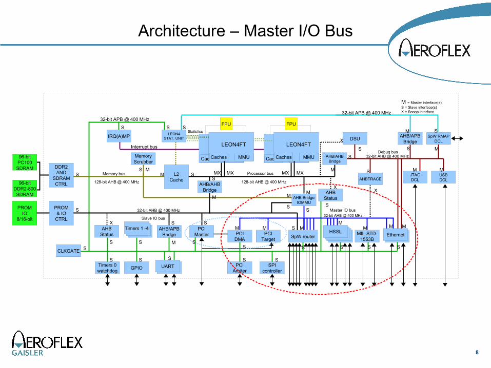
Architecture – Master I/O Bus
L2Cache
PCIMaster
128-bit AHB @ 400 MHz
32-bit AHB @ 400 MHz
Processor bus
Slave IO bus
PROM& IO
CTRL
PROMIO
8/16-bit
HSSLSpW router
USBDCL
MemoryScrubber
128-bit AHB @ 400 MHz
Memory bus
UARTGPIO
DSU
AHBStatus
JTAGDCL
AHB/APBBridge
AHB/AHBBridge
PCITarget
PCIDMA
Ethernet
AHB BridgeIOMMU
AHB/AHBBridge
32-bit AHB @ 400 MHz
Master IO bus
32-bit AHB @ 400 MHzDebug bus
32-bit APB @ 400 MHz
SpW RMAPDCL
AHBStatus
PCIArbiter
EthernetHSSLHSSLHSSL
UART
S S SS S S
SS
S
S
S
SM
SMM
M
M MM
MMM
M
MS
S
S S S
M = Master interface(s)S = Slave interface(s)X = Snoop interface
X
X
MX
S
X
M
SM
S
S
MX
IRQ(A)MP
Timers 0watchdog
S
S
MX MX
CLKGATE S
AHBTRACE
AHB/APBBridge
32-bit APB @ 400 MHz
LEON4STAT. UNIT
S
M
M SS
Timers 1 -4 S
X
S
M
Statistics
Interrupt bus
Caches MMU
FPU
FPU
Caches MMU
IRQCTRL
LEON4FTCaches MMU
LEON4FT
FPU
FPUIRQCTRL
LEON4FTCaches MMU
LEON4FT
S
SPIcontroller
S
96-bitDDR2-800SDRAM
96-bitPC100
SDRAM DDR2AND
SDRAMCTRL
MIL-STD-1553B
M
S

9
Architecture – Slave I/O Bus
L2Cache
PCIMaster
128-bit AHB @ 400 MHz
32-bit AHB @ 400 MHz
Processor bus
Slave IO bus
PROM& IO
CTRL
PROMIO
8/16-bit
HSSLSpW router
USBDCL
MemoryScrubber
128-bit AHB @ 400 MHz
Memory bus
UARTGPIO
DSU
AHBStatus
JTAGDCL
AHB/APBBridge
AHB/AHBBridge
PCITarget
PCIDMA
Ethernet
AHB BridgeIOMMU
AHB/AHBBridge
32-bit AHB @ 400 MHz
Master IO bus
32-bit AHB @ 400 MHzDebug bus
32-bit APB @ 400 MHz
SpW RMAPDCL
AHBStatus
PCIArbiter
EthernetHSSLHSSLHSSL
UART
S S SS S S
SS
S
S
S
SM
SMM
M
M MM
MMM
M
MS
S
S S S
M = Master interface(s)S = Slave interface(s)X = Snoop interface
X
X
MX
S
X
M
SM
S
S
MX
IRQ(A)MP
Timers 0watchdog
S
S
MX MX
CLKGATE S
AHBTRACE
AHB/APBBridge
32-bit APB @ 400 MHz
LEON4STAT. UNIT
S
M
M SS
Timers 1 -4 S
X
S
M
Statistics
Interrupt bus
Caches MMU
FPU
FPU
Caches MMU
IRQCTRL
LEON4FTCaches MMU
LEON4FT
FPU
FPUIRQCTRL
LEON4FTCaches MMU
LEON4FT
S
SPIcontroller
S
96-bitDDR2-800SDRAM
96-bitPC100
SDRAM DDR2AND
SDRAMCTRL
MIL-STD-1553B
M
S

10
Architecture - Debug Bus
L2Cache
PCIMaster
128-bit AHB @ 400 MHz
32-bit AHB @ 400 MHz
Processor bus
Slave IO bus
PROM& IO
CTRL
PROMIO
8/16-bit
HSSLSpW router
USBDCL
MemoryScrubber
128-bit AHB @ 400 MHz
Memory bus
UARTGPIO
DSU
AHBStatus
JTAGDCL
AHB/APBBridge
AHB/AHBBridge
PCITarget
PCIDMA
Ethernet
AHB BridgeIOMMU
AHB/AHBBridge
32-bit AHB @ 400 MHz
Master IO bus
32-bit AHB @ 400 MHzDebug bus
32-bit APB @ 400 MHz
SpW RMAPDCL
AHBStatus
PCIArbiter
EthernetHSSLHSSLHSSL
UART
S S SS S S
SS
S
S
S
SM
SMM
M
M MM
MMM
M
MS
S
S S S
M = Master interface(s)S = Slave interface(s)X = Snoop interface
X
X
MX
S
X
M
SM
S
S
MX
IRQ(A)MP
Timers 0watchdog
S
S
MX MX
CLKGATE S
AHBTRACE
AHB/APBBridge
32-bit APB @ 400 MHz
LEON4STAT. UNIT
S
M
M SS
Timers 1 -4 S
X
S
M
Statistics
Interrupt bus
Caches MMU
FPU
FPU
Caches MMU
IRQCTRL
LEON4FTCaches MMU
LEON4FT
FPU
FPUIRQCTRL
LEON4FTCaches MMU
LEON4FT
S
SPIcontroller
S
96-bitDDR2-800SDRAM
96-bitPC100
SDRAM DDR2AND
SDRAMCTRL
MIL-STD-1553B
M
S
11
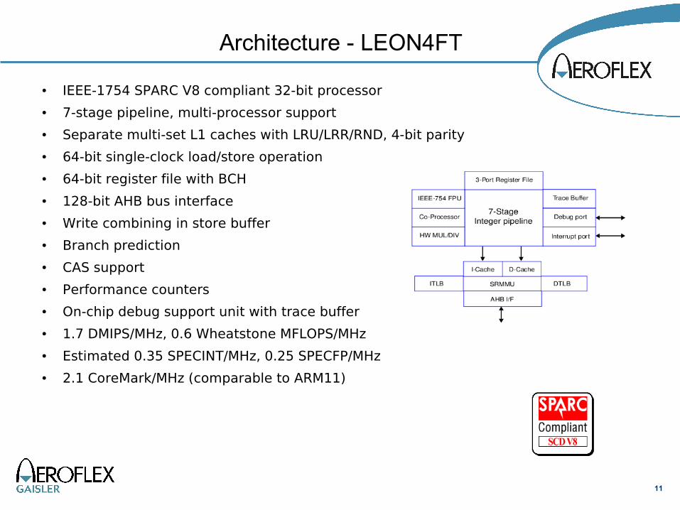
● IEEE-1754 SPARC V8 compliant 32-bit processor
● 7-stage pipeline, multi-processor support
● Separate multi-set L1 caches with LRU/LRR/RND, 4-bit parity
● 64-bit single-clock load/store operation
● 64-bit register file with BCH
● 128-bit AHB bus interface
● Write combining in store buffer
● Branch prediction
● CAS support
● Performance counters
● On-chip debug support unit with trace buffer
● 1.7 DMIPS/MHz, 0.6 Wheatstone MFLOPS/MHz
● Estimated 0.35 SPECINT/MHz, 0.25 SPECFP/MHz
● 2.1 CoreMark/MHz (comparable to ARM11)
Architecture - LEON4FT
12
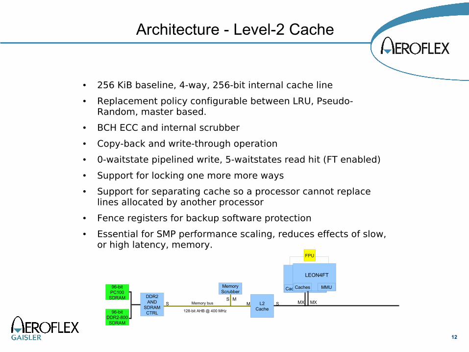
● 256 KiB baseline, 4-way, 256-bit internal cache line
● Replacement policy configurable between LRU, Pseudo-Random, master based.
● BCH ECC and internal scrubber
● Copy-back and write-through operation
● 0-waitstate pipelined write, 5-waitstates read hit (FT enabled)
● Support for locking one more more ways
● Support for separating cache so a processor cannot replace lines allocated by another processor
● Fence registers for backup software protection
● Essential for SMP performance scaling, reduces effects of slow, or high latency, memory.
Architecture - Level-2 Cache
L2Cache
MemoryScrubber
128-bit AHB @ 400 MHz
Memory busSM
SM MXS
MX
Caches MMU
FPU
FPUIRQCTRL
LEON4FTCaches MMU
LEON4FT
96-bitDDR2-800SDRAM
96-bitPC100
SDRAM DDR2AND
SDRAMCTRL

13
● Can access external DDR2/SDRAM and on-chip SDRAM
● Performs the following operations:
● Initialization
● Scrubbing
● Memory re-generation
● Configurable by software
● Counts correctable errors with option to alert CPU
● Supports, together with DDR2 SDRAM and SDRAM memory controller, on-line code switch in case of permanent device failure
Architecture - Memory scrubber
L2Cache
MemoryScrubber
128-bit AHB @ 400 MHz
Memory busSM
MS
96-bitDDR2-800SDRAM
96-bitPC100
SDRAM DDR2AND
SDRAMCTRL
14
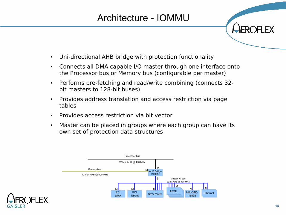
● Uni-directional AHB bridge with protection functionality
● Connects all DMA capable I/O master through one interface onto the Processor bus or Memory bus (configurable per master)
● Performs pre-fetching and read/write combining (connects 32-bit masters to 128-bit buses)
● Provides address translation and access restriction via page tables
● Provides access restriction via bit vector
● Master can be placed in groups where each group can have its own set of protection data structures
Architecture - IOMMU
128-bit AHB @ 400 MHz
Processor bus
HSSLSpW routerPCI
TargetPCI
DMAEthernet
AHB BridgeIOMMU
32-bit AHB @ 400 MHz
Master IO bus
EthernetHSSLHSSLHSSL
M
MM
MMM
S
M
MIL-STD-1553B
M
Memory bus
128-bit AHB @ 400 MHz

15
● The standard LEON3/4 multiprocessor interrupt controller has been extended to support AMP configurations
● Controller in NGMP has four internal interrupt controllers
● Each processor can be dynamically routed to one of these (internal) controllers
Architecture - Interrupt controller
16
Architecture - Separation
● Measures taken to improve separation include:
● Extension of interrupt controller, multiple timer units
● Peripheral register areas start on page boundaries
● Inclusion of IOMMU
● Separation is accomplished by relying on
● Processor memory management units
● I/O memory management unit
● L2 cache fence registers
● The current hardware support for separation should provide efficient protection against misbehaving software and unwanted external accesses (for instance from PCI/RMAP)
● Shared resources that will lead to SW instances affecting each other:
● Shared AMBA buses/L2 cache/memory controller
● FPU sharing
17
● We will now look at some high level “use cases” for the NGMP architecture:
● Symmetric multiprocessing configurations
● Asymmetric multiprocessing configurations
● PROM-less booting
● SpaceWire router/bridge
How to use NGMP

18
● Symmetric multiprocessing is supported by configuring all LEON4 cores to use the same interrupt controller.
● SMP configurations with 2 – 4 processors are supported
● Operating systems that support SMP for LEON include:
● Linux 2.6+
● VxWorks 6.7
● eCos
● RTEMS (work is progressing)
How to use NGMP – SMP
19
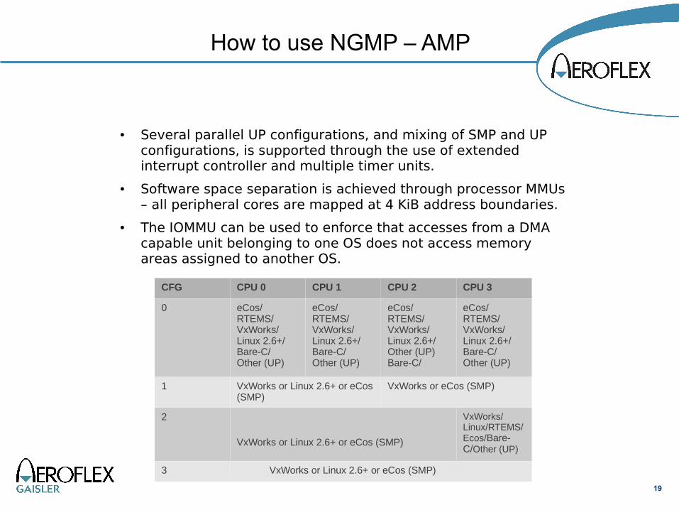
CFG CPU 0 CPU 1 CPU 2 CPU 3
0 eCos/RTEMS/VxWorks/Linux 2.6+/Bare-C/Other (UP)
eCos/RTEMS/VxWorks/Linux 2.6+/Bare-C/Other (UP)
eCos/RTEMS/VxWorks/Linux 2.6+/Other (UP)Bare-C/
eCos/RTEMS/VxWorks/Linux 2.6+/Bare-C/Other (UP)
1 VxWorks or Linux 2.6+ or eCos (SMP)
VxWorks or eCos (SMP)
2
VxWorks or Linux 2.6+ or eCos (SMP)
VxWorks/Linux/RTEMS/Ecos/Bare-C/Other (UP)
3 VxWorks or Linux 2.6+ or eCos (SMP)
● Several parallel UP configurations, and mixing of SMP and UP configurations, is supported through the use of extended interrupt controller and multiple timer units.
● Software space separation is achieved through processor MMUs – all peripheral cores are mapped at 4 KiB address boundaries.
● The IOMMU can be used to enforce that accesses from a DMA capable unit belonging to one OS does not access memory areas assigned to another OS.
How to use NGMP – AMP

20
Taking advantage of the four LEON4FT
● Advantage: More processing power, more functions on one chip
● Design goal of maximum average performance has a cost in jitter/predictability
● Our general recommendation: Use a simple SMP OS
● Linux/VxWorks/eCos with SMP support
● Developers hesitant to trust an SMP kernel
● UP instances of RTEMS/VxWorks/eCos/Bare-C/Other can be used by linking images to separate memory areas
● Booting multiple images is supported by MKPROM2
● May need static MMU tables to enforce separation
● Developer need to assign hardware resources
● But apart from added work on setup, no news● More functions on one chip● The cost is increased jitter

21
PROM-less / SpW applications
● PROM-less booting possible via SpaceWire
● Connect via RMAP
● Configure main memory controller
● Use HW memory scrubber to initialize memory
● Enable L2 cache
● Upload software
● Assign processor start address(es)
● Start processor(s)
● SpaceWire router, with eight external ports, is fully functional without processor intervention
● Device can also act as a software/processor-free bridge between SpW and PCI/SPI/1553 etc.
● IOMMU can be used to restrict RMAP access
22
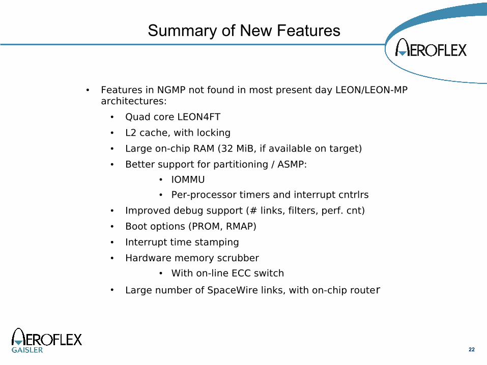
● Features in NGMP not found in most present day LEON/LEON-MP architectures:
● Quad core LEON4FT
● L2 cache, with locking
● Large on-chip RAM (32 MiB, if available on target)
● Better support for partitioning / ASMP: ● IOMMU● Per-processor timers and interrupt cntrlrs
● Improved debug support (# links, filters, perf. cnt)
● Boot options (PROM, RMAP)
● Interrupt time stamping
● Hardware memory scrubber● With on-line ECC switch
● Large number of SpaceWire links, with on-chip router
Summary of New Features

23
Benchmarks - Overview
● Benchmarks
● I/O traffic
● FPU sharing
● Scaling
● Comparison with AT697, UT699, GR712RC
24
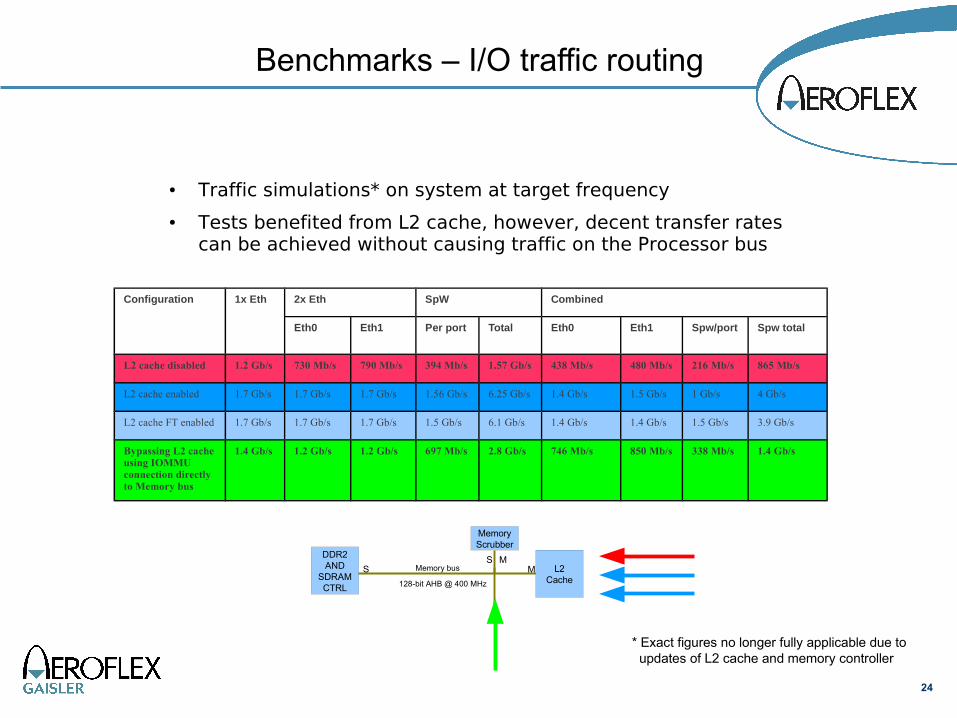
Benchmarks – I/O traffic routing
● Traffic simulations* on system at target frequency
● Tests benefited from L2 cache, however, decent transfer rates can be achieved without causing traffic on the Processor bus
Configuration 1x Eth 2x Eth SpW Combined
Eth0 Eth1 Per port Total Eth0 Eth1 Spw/port Spw total
L2 cache disabled 1.2 Gb/s 730 Mb/s 790 Mb/s 394 Mb/s 1.57 Gb/s 438 Mb/s 480 Mb/s 216 Mb/s 865 Mb/s
L2 cache enabled 1.7 Gb/s 1.7 Gb/s 1.7 Gb/s 1.56 Gb/s 6.25 Gb/s 1.4 Gb/s 1.5 Gb/s 1 Gb/s 4 Gb/s
L2 cache FT enabled 1.7 Gb/s 1.7 Gb/s 1.7 Gb/s 1.5 Gb/s 6.1 Gb/s 1.4 Gb/s 1.4 Gb/s 1.5 Gb/s 3.9 Gb/s
Bypassing L2 cache using IOMMU connection directly to Memory bus
1.4 Gb/s 1.2 Gb/s 1.2 Gb/s 697 Mb/s 2.8 Gb/s 746 Mb/s 850 Mb/s 338 Mb/s 1.4 Gb/s
* Exact figures no longer fully applicable due to updates of L2 cache and memory controller
L2Cache
MemoryScrubber
128-bit AHB @ 400 MHz
Memory busSM
MS
DDR2AND
SDRAMCTRL
25
Benchmarks – FPU sharing (0)
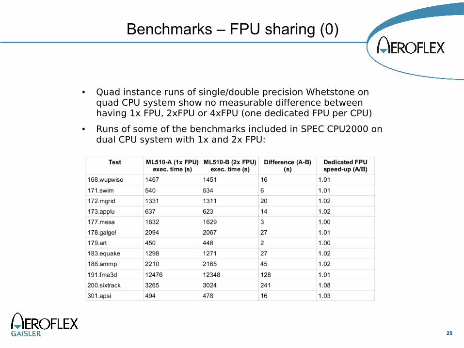
● Quad instance runs of single/double precision Whetstone on quad CPU system show no measurable difference between having 1x FPU, 2xFPU or 4xFPU (one dedicated FPU per CPU)
● Runs of some of the benchmarks included in SPEC CPU2000 on dual CPU system with 1x and 2x FPU:
26
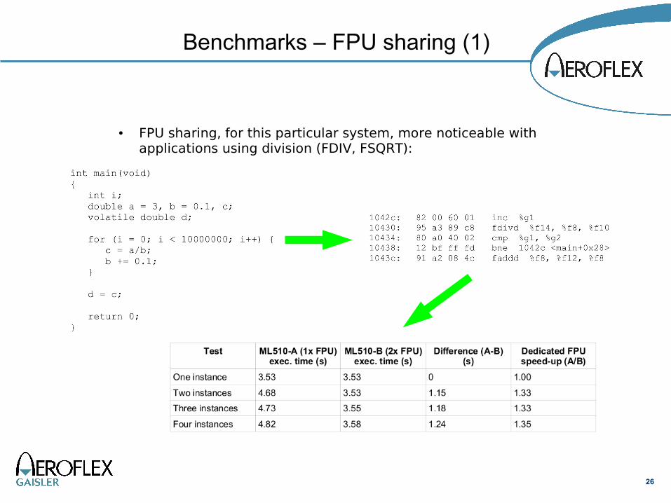
Benchmarks – FPU sharing (1)
● FPU sharing, for this particular system, more noticeable with applications using division (FDIV, FSQRT):

27
Benchmarks – Scaling (0)
● Running gcc, parser, eon, twolf, applu and art CPU2000 benchmarks first sequentially and then in parallel on one to four cores:
4 seq inst / 1 core4 par inst / 1 core
4 par inst / 2 cores4 par inst / 3 cores
4 par inst / 4 cores1 inst / 1 core
0
2000
4000
6000
8000
10000
12000
14000
Benchmark
Exe
cutio
n ti
me
43% increase in exec time4x the amount of work
Speed-up is 2.91 whengoing to four cores
28
4 par inst / 4 cores1 inst / 1 core
0
1000
2000
3000
4000
5000
Exe
cutio
n ti
me
(s)
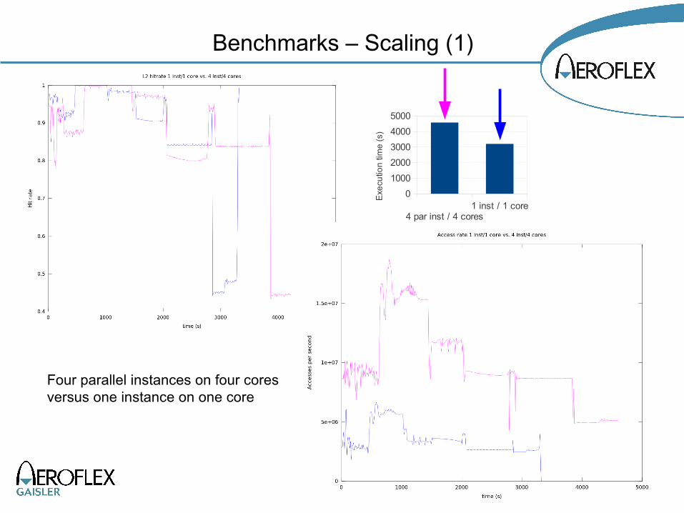
Benchmarks – Scaling (1)
Four parallel instances on four coresversus one instance on one core
29
4 par inst / 1 core4 par inst / 4 cores
02000400060008000
100001200014000
Exe
cutio
n ti
me
(s)
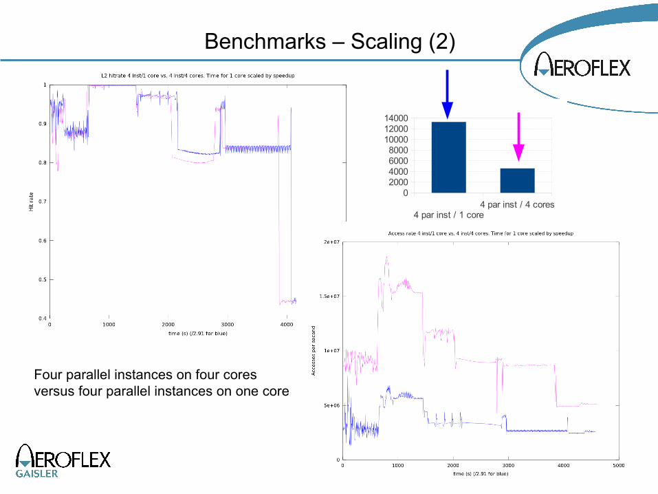
Benchmarks – Scaling (2)
Four parallel instances on four coresversus four parallel instances on one core

30
Benchmarks - Comparison
● Comparison with existing processors targeted for space
● Benchmark scores relative to AT697:
Benchmark AT697 UT699 GR712RC NGMP
164.gzip 1 0.94 (0.66) 1.1 (1.1) 1.31 (5.24)176.gcc 1 0.79 (0.55) 0.97 (0.97) 1.3 (5.2)256.bzip2 1 0.93 (0.65) 1.06 (1.06) 1.33 (5.32)AOCS 1 1.2 (0.84) 1.52 (1.52) 1.79 (7.16)Basicmath 1 1.3 (0.91) 1.46 (1.46) 1.62 (6.48)Coremark, 1 thread 1 0.89 (0.62) 1.09 (1.09) 1.21 (4.84)Coremark, 4 threads 1 0.89 (0.62) 2.05 (2.05) 4.59 (18.36)Dhrystone 1 0.94 (0.66) 1.05 (1.05) 1.39 (5.56)Dhrystone, 4 instances 1 0.94 (0.66) 1.61 (1.61) 4.81 (19.24)Linpack 1 1.2 (0.84) 1.26 (1.26) 1.71 (6.84)Whetstone 1 1.94 (1.36) 2 (2) 2.22 (8.88)Whetstone, 4 instances 1 1.94 (1.36) 3.7 (3.7) 8.68 (34.72)
All benchmarks were compiled with GCC-4.3.2 tuned for SPARC V8. All systems were clocked at 50 MHz during the tests, using 32-bit SDRAM (LEON2/3) or 64-bit DDR2 (NGMP)Note that the maximum operating frequency of the devices differ, here all tests are run at 50 MHzValues in parentheses are scaled for maximum frequency.

31
● NGMP simulator based on GRSIM
● C-models of IP cores linked into final simulator
● Re-entrant and thread-safe library
● Accuracy goal is 90% over extended period
● NGMP is fully supported by GRMON/GRMON2 debug tools
● Complemented by standard RTOS trace tools
Simulator and Debugger

32
● Functional prototype on evaluation board is expected to be available Q2 2012
● Will not include HSSL, nor large on-chip RAM
● Includes both DDR2 and SDR SDRAM on separate pins
● FPGA prototypes with reduced NGMP designs available now
● Xilinx ML510, Synopsys HAPS-51, TerASIC DE2
● Aeroflex Gaisler GR-CPCI-XC4V with LX200 FPGA
● Aeroflex Gaisler GR-PCI-XC5V
Prototypes

33
Thank you for listening
For updates and to download the NGMP specification, please see:
http://microelectronics.esa.int/ngmp/ngmp.htm

34
● Fault-tolerance in the NGMP system is aimed at detecting and correcting SEU errors in on-chip and off-chip RAM
● L1 cache and register files in LEON4FT are protected using parity and BCH
● L2 cache will use BCH
● External SDRAM will be protected using Reed-Solomon
● Boot PROM will use BCH
● RAM blocks in on-chip IP cores will be protected using BCH or TMR, smaller buffers can be synthesized as flip-flops
● Flip-flops will be protected with SEU-hardened library cells if available or TMR otherwise
Extra: Fault-Tolerance Summary
35
The NGMP has improved debugging support compared to the LEON2FT
and many existing LEON3 implementations. The new features include:
● Several high-speed debug interfaces
● Non-intrusive debugging through dedicated Debug bus
● AHB trace buffer with filtering
● Instruction trace buffer with filtering
● Hardware data watchpoints
Extra: Improved Debugging Support

36
Extra: Improved Profiling Support (0)
The NGMP has improved profiling support compared to the LEON2FT and LEON3. The new features allow to measure the following metrics:
● Processor statistics
● Instruction/Data cache/TLB miss/hold
● Data write buffer hold
● Total/Integer/FP instruction count
● Branch predication miss
● Total execution time (excluding debug mode)
● Special filters allow counting number of:● Integer branches● CALL instructions● Regular type 2 instructions● LOAD and STORE instructions● LOAD instructions● STORE and instructions
37
Extra: Improved Profiling Support (1)
In addition the processor statistics you can also measure:
● L2 cache hit/miss rate
● AHB utilization
● AHB utilization per master
● Total AHB utilization
● Interrupt time stamp unit allows users to measure interrupt handler latencies

38
● Baseline is ST 65nm space technology
● Requirements
● DDR2 PHY
● I/O standards: LVTTL, SSTL, PCI
● Memory: ● 1-port RAM, 2-port RAM● High density 1-port RAM/SDRAM
● Backup options:
● UMC 90 nm with DARE library
● Tower 130 nm with Ramon library
● FP target technology: eASIC Nextreme2
Extra: Target technology