
New Product Introduction - Rutronik elektronische ......Supports fast charging for Samsung and Apple...
11
New Product Introduction OptiMOS TM 5 40V MOSFET Normal Level in SuperSO8 5x6 sTOLL - new 7x8 mm 2 Power MOS package OPTIREG™ Power Management IC (PMIC) TLF30682, TLF30681 Extension of CoolSiC™ MOSFET Easy portfolio with TIM EasyPACK™ 3B with TRENCHSTOP™ IGBT7 for 1500 V PV string inverters EiceDRIVER™ WCDSC006 - Half-bridge level-shift gate-driver IC REF_10WTX_QI_4102 - 15W Qi transmitter for charging BCR431U - Linear low-voltage-drop LED driver IC XENSIV™ Sense2GoL pulse development kit KIT_6W_13V_P7_950V - Auxiliary DC-DC supply solution June 2020
Transcript of New Product Introduction - Rutronik elektronische ......Supports fast charging for Samsung and Apple...

New Product Introduction
OptiMOSTM 5 40V MOSFET Normal Level in SuperSO8 5x6
sTOLL - new 7x8 mm2 Power MOS package
OPTIREG™ Power Management IC (PMIC) TLF30682, TLF30681
Extension of CoolSiC™ MOSFET Easy portfolio with TIM
EasyPACK™ 3B with TRENCHSTOP™ IGBT7 for 1500 V PV string inverters
EiceDRIVER™ WCDSC006 - Half-bridge level-shift gate-driver IC
REF_10WTX_QI_4102 - 15W Qi transmitter for charging
BCR431U - Linear low-voltage-drop LED driver IC
XENSIV™ Sense2GoL pulse development kit
KIT_6W_13V_P7_950V - Auxiliary DC-DC supply solution
June 2020

OptiMOSTM 5 40 V MOSFET Normal Level in SuperSO8 5x6
With the OptiMOSTM 5 40 V normal level product family Infineon offers a
benchmark solution for applications requiring normal level (higher
threshold voltage) drive capability.
The high Vth in the normal level portfolio offers immunity to false turn-on
due to noisy environments. In addition, lower QGD/QGS ratios (CGD/CGS
divider ratio) reduce the peak of the gate voltage spikes, further
contributing to the robustness against unwanted turn-on.
Benefits
Normal gate drive offers immunity to false turn-on in noisy environments
Increased operating temperature for robust designs
Reduced switching losses leading to greater system efficien-
cy and power density
Suitable for operation at higher frequencies enabling ad-vanced motor control techniques like field oriented control (FOC), direct torque control (DTC) as well as block commuta-tion method
Capable of withstanding high surge current during in-rush, locked rotor and braking scenarios
Increased current carrying capability
Product collaterals / Online support
Product family page
Product brief
Application diagram
Features
Normal Level gate threshold (2.8 V typical)
175°C junction temperature (Tj)
Optimized charge ratio QGD/QGS <0.8 for dv/dt and noise immunity
Low gate charge
Strong linear mode /SOA rating
High current rating
Target applications
Battery powered applications
Battery powered tools
Battery management
Low voltage drives
Product overview incl. data sheet link
OPN SP Number Package
ISC015N04NM5ATMA1 SP005352240 SuperSO8
ISC017N04NM5ATMA1 SP005399103 SuperSO8
ISC019N04NM5ATMA1 SP005352244 SuperSO8
ISC028N04NM5ATMA1 SP005399107 SuperSO8
ISC036N04NM5ATMA1 SP005399111 SuperSO8
ISC046N04NM5ATMA1 SP005399115 SuperSO8
ISC058N04NM5ATMA1 SP005399119 SuperSO8

sTOLL - new 7x8 mm2 Power MOS package
New OptiMOS™-6 40 V Mosfet in sTOLL Package (high power
leadless package in 7x8 mm2) for future automotive applications
(JEDEC name is MO-319A and IEC name is HSOF-5).
sTOLL offers high current capability of 250 A and a footprint of 56
mm2 which is even smaller than DPAK (65 mm2). In combination
with Infineon’s leading OptiMOS™-6 40 V power MOS technology,
sTOLL offers best in class power density and power efficiency at
Infineon’s well known quality level for robust automotive
packages.
Benefits
High power + current density
High thermal capacity
lead-frame package
Reduced conduction losses
Optimized switching behavior
Reduced form factor compared to traditional DPAK/D2PAK
Industry standard package (JEDEC MO-319A)
Product collaterals / Online support
Product Page
Product brief
Application diagram
Features
JEDEC registered
7x8 mm² small footprint
250 A high current capability
Leadless package with low package resistance and minimized stray inductance
Leading 40 V technology OptiMOS-5TM + OptiMOS-6TM
RDS(on) range: 0,6 mOhm – 1,4 mOhm
AOI capable package for Automated optical inspection
Target applications
12 V EPS
12 V BLDC
12 V - 48 V DC/DC
Product overview incl. data sheet link
OPN SP Number Package
IAUA250N04S6N006AUMA1 SP003127488 PG-HSOF-5
IAUA250N04S6N007AUMA1 SP003127494 PG-HSOF-5
IAUA200N04S5N010AUMA1 SP001497688 PG-HSOF-5
IAUA180N04S5N012AUMA1 SP002655470 PG-HSOF-5
IAUA180N04S5N012AUMA1 SP001497666 PG-HSOF-5

OPTIREG™ Power Management IC (PMIC) TLF30682, TLF30681
Automotive PMICs, capable to withstand a battery connection at the
input, supplying 3 different voltage domains at the outputs optimized
to power different loads such a CAN transceiver, memory modules
and the core of a microcontroller. The devices integrate internal and
external voltage monitoring and feature a window watchdog in a
7x7mm² VQFN-48 package.
Benefits
High efficiency and flexibility
Wide temperature range
Reduced number of external components for minimized PCB-area
Minimized values of external components for cost optimization
Product collaterals / Online support
Product family page
Product brief TLF30681QVS01
Product brief TLF30682QVS01
TLF30681 Simulation Models
TLF30682 Simulation Models
Block diagram
Features
Pre-/post-regulator concept: Buck/SMPR-Buck & SMPR-Boost –µC or MMIC or DSP –Core or memory –Transceivers
UV/OV-monitoring for integrated rails
UV/OV-monitoring for external rails
Flexible window-watchdog
Competitive advantage
Small footprint
Reduced number of external components and minimized value
of those
Automotive grade with wide temperature range
Minimized values external components for cost optimization
High system reliability
Easy and fast implementation
Safety documents available on request
Target applications TLF30682
76-79 GHz radar
Multi-purpose camera
Human machine interface
Target applications TLF30681
77 GHz SRR (Short Range Radar)
24 GHz radar
60 GHz radar (In-cabin sensing)
Product overview incl. data sheet link
OPN SP Number Package
TLF30682QVS01XUMA1 SP001588618 PG-VQFN-48
TLF30682QVS01BOARDTOBO1 SP001622202 board
TLF30681QVS01XUMA1 SP005347674 PG-VQFN-48
TLF30681QVS01BOARDTOBO1 SP005427058 board
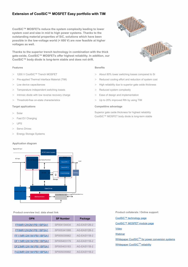
Extension of CoolSiC™ MOSFET Easy portfolio with TIM
CoolSiC™ MOSFETs reduce the system complexity leading to lower
system cost and size in mid to high power systems. Thanks to the
outstanding material properties of SiC, solutions which have been
possible in the low-voltage world (< 600 V) are now feasible at higher
voltages as well.
Thanks to the superior trench technology in combination with the thick
gate-oxide, CoolSiC™ MOSFETs offer highest reliability. In addition, our
CoolSiC™ body diode is long-term stable and does not drift.
Benefits
About 80% lower switching losses compared to Si
Reduced cooling effort and reduction of system cost
High reliability due to superior gate oxide thickness
Reduced system complexity
Ease of design and implementation
Up to 20% improved Rth by using TIM
Product collaterals / Online support
CoolSiC™ technology page
CoolSiC™ MOSFET module page
Video
Webinar
Whitepaper CoolSICTM for power conversion systems
Whitepaper CoolSICTM reliability
Application diagram
Features
1200 V CoolSiC™ Trench MOSFET
Pre-applied Thermal Interface Material (TIM)
Low device capacitances
Temperature independent switching losses
Intrinsic diode with low reverse recovery charge
Threshold-free on-state characteristics
Competitive advantage
Superior gate oxide thickness for highest reliability
CoolSiC™ MOSFET body diode is long-term stable
Target applications
Solar
Fast EV Charging
UPS
Servo Drives
Energy Storage Systems
Product overview incl. data sheet link
OPN SP Number Package
FF6MR12W2M1PB11BPSA1 SP004134434 AG-EASY2B-2
FF8MR12W2M1PB11BPSA1 SP005341588 AG-EASY2B-2
FF11MR12W1M1PB11BPSA1 SP005035982 AG-EASY1B-2
DF11MR12W1M1PB11BPSA1 SP005403179 AG-EASY1B-2
DF23MR12W1M1PB11BPSA1 SP005403183 AG-EASY1B-2
F423MR12W1M1PB11BPSA1 SP005035992 AG-EASY1B-2

EasyPACK™ 3B with TRENCHSTOP™ IGBT7 for 1500 V PV string inverters
The solar power market is undergoing a trend towards 1500 V
solutions, which allow for more series connections, less cable, fewer
generator connection boxes and fewer inverters.
The new EasyPACK™ 3B with TRENCHSTOP™ IGBT7 is especially
designed for this market; it offers not only the established flexible pin
-grid system to realize customized solutions, but the 950 V Active
Neutral Point-Clamping (ANPC) topology can generate alternating
current from 1500 V direct current with particularly low loss levels.
EasyPACK™ 3B is a total solution for 1500 V solar inverters. For
MPPT (Maximum Power Point Tracker), Infineon offers a single
module solution in dual-boost topology with 3 MPPTs in one module.
Each of the MPPT can handle up to 26 A current. This makes this
solution ready for bi-facial solar panels.
For the inverter stage, Infineon offers two solutions: one with Si
diodes and one with CoolSiC™ Schottky diodes. The EasyPACK™ 3B
with TRENCHSTOP™ IGBT7 and CoolSiC™ Schottky diode can
achieve up to 10% higher power density.
Benefits
Extend the well-known Easy power module family
Achieve higher power with only a few mechanical modifications for
current inverter designs
Voltage class and topology result in extreme low losses for a given
power rating < 150 kW
Pin-out allows fast switching speed for achieving low loss
PressFIT pins are the best fit for automated, high-volume produc-tion
Product collaterals / Online support
Family Page Easy Power Modules
Family page TRENCHSTOP™ IGBT7
Whitepaper
Video
Application diagram
Features
Innovative base-plate-less power module in Easy 3B housing
400 A nominal current
Optimized voltage class (950 V) in 3-level ANPC topology
Low parasitic inductance pin-out design
Press-FIT pins
Integrated NTC
Two options: Si or CoolSiC™ Schottky diode
Competitive advantage
Broadest 12 mm portfolio without baseplate on the market to cover ap-plications from 600 V to 1700 V
Target applications
Solar string inverter solutions
Product overview incl. data sheet link
OPN SP Number Package
F3L400R10W3S7B11BPSA1 SP003503062 AG-EASY3B-1
F3L400R10W3S7FB11BPSA1 SP003723550 AG-EASY3B-1
FS3L200R10W3S7FB11BPSA1 SP003733416 AG-EASY3B-1

EiceDRIVER™ WCDSC006 - Half-bridge level-shift gate-driver IC
The half-bridge gate driver EiceDRIVER™ WCDSC006 is particularly
suitable to drive both high-side and low-side MOSFETs in a half-
bridge inverter configuration especially in inductive wireless power
charging technology for smartphones.
Benefits
Increased robustness
Faster switching mode and higher efficiency results
Increase flexibility
No need of external components
Higher margin and more robust operation
No risk of cross conduction
Product collaterals / Online support
Product page
Product brief
Block diagram
Features
-0.3 V to 7 V input bin capability
4 A sink and 2 A source current capability for high-side and lo-
side drivers
Independent high-side / low-side TTL logic inputs
Integrated bootstrap diode
Maximum bootstrap voltage of 60 V
5 ns (typ) dead-time to prevent shoot-through
Target applications
Wireless charging
Product overview incl. data sheet link
OPN SP Number Package
WCDSC006XUMA1 SP002574622 PG-WSON-10

REF_10WTX_QI_4102 - 15W Qi transmitter for charging smartphones
The 15W wireless power transmitter evaluation module is a high-
performance, easy-to-use development kit designed for applications
up to 15W of power transfer. It supports an input voltage range of 9-
12V and is compatible with QC 3.0 adapters.
The transmitter provides the designer a certified platform that
drastically reduces the development time of their end application.
The system supports WPC v1.2.4 receivers up to 15W. Smartphones
with proprietary fast charge capability are also supported.
Benefits
Development effort reduction
Efficiency and accurate FOD
Reduced system costs
Fast charging capability
Product collaterals / Online support
Product page
Interactive 3D board model
Solution brief
Quick start guide
Solution diagram
Features
Up to 15W wireless power transfer
WPC Qi v1.2.4 EPP certified (MP-A11 coil)
Fixed frequency power transfer
Supports fast charging for Samsung and Apple phones
VIN range: 9 -12V and 83% peak efficienc
To be operated with Q.C. 3.0 adapter
Improved accuracy of foreign object detection (FOD)
Target applications
Mobile phone, tablet
Electric toys
IoT (Medical, health, smart home)
Wireless charging
Product overview incl. product page link
OPN SP Number Package
REF10WTXQI4102TOBO1 SP003078392 board
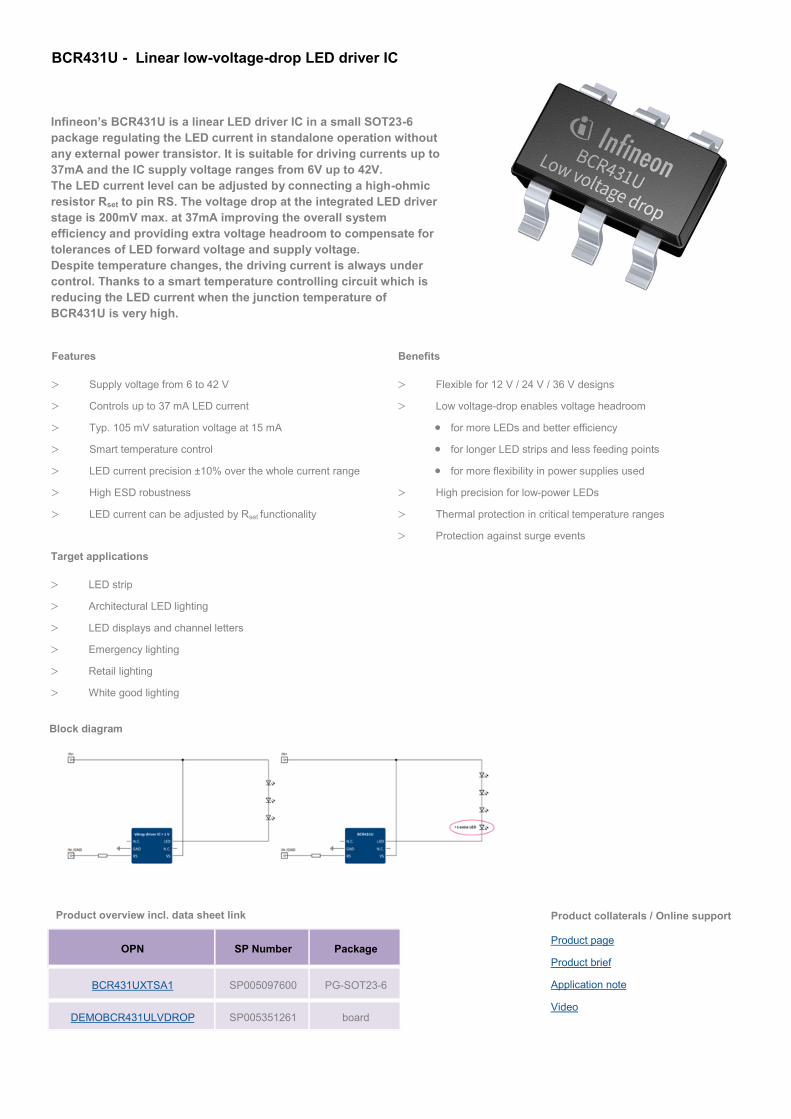
BCR431U - Linear low-voltage-drop LED driver IC
Infineon’s BCR431U is a linear LED driver IC in a small SOT23-6
package regulating the LED current in standalone operation without
any external power transistor. It is suitable for driving currents up to
37mA and the IC supply voltage ranges from 6V up to 42V.
The LED current level can be adjusted by connecting a high-ohmic
resistor Rset to pin RS. The voltage drop at the integrated LED driver
stage is 200mV max. at 37mA improving the overall system
efficiency and providing extra voltage headroom to compensate for
tolerances of LED forward voltage and supply voltage.
Despite temperature changes, the driving current is always under
control. Thanks to a smart temperature controlling circuit which is
reducing the LED current when the junction temperature of
BCR431U is very high.
Benefits
Flexible for 12 V / 24 V / 36 V designs
Low voltage-drop enables voltage headroom
for more LEDs and better efficiency
for longer LED strips and less feeding points
for more flexibility in power supplies used
High precision for low-power LEDs
Thermal protection in critical temperature ranges
Protection against surge events
Product collaterals / Online support
Product page
Product brief
Application note
Video
Block diagram
Features
Supply voltage from 6 to 42 V
Controls up to 37 mA LED current
Typ. 105 mV saturation voltage at 15 mA
Smart temperature control
LED current precision ±10% over the whole current range
High ESD robustness
LED current can be adjusted by Rset functionality
Target applications
LED strip
Architectural LED lighting
LED displays and channel letters
Emergency lighting
Retail lighting
White good lighting
Product overview incl. data sheet link
OPN SP Number Package
BCR431UXTSA1 SP005097600 PG-SOT23-6
DEMOBCR431ULVDROP SP005351261 board

XENSIV™ Sense2GoL pulse development kit
This development kit allows the user to implement and test several
sensing applications at the 24 GHz ISM band such as motion
detection and speed measurement. The kit operates in a pulsed
mode achieving 18 m detection range with a sensor power
consumption less than 5 mW. The demonstration kit consists of two
boards, the radar front end board: SHIELD_BGT24LTR11 and the
microcontroller board: RADAR BB XMC4700. The baseboard adds
additional flexibility by allowing battery operation, current
measurements, SD card reader for storage and Arduino compatible
pin connectors.
Benefits
Fast prototyping with flexible kit
Arduino Library available
Can be battery driven
Covers multiple applications/use cases
Product collaterals / Online support
Product page
Product brief
Application notes
3D model
Video
Block diagram
Features
Capability to detect motion, speed and direction of movement (approaching or retreating)
Detection range of 18 m for human target at a power consump-tion < 5 mW ›High sensitivity of detection in comparison to PIR
Operates in harsh environments and detects through non-metallic materials
Multiple power supply possibilities: Micro USB, external power supply, or battery
Arduino compatible microcontroller board (Arduino standard connectors)
Modulation parameters can be changed to suit the application requirements
Multiple current sensors for current consumption monitoring and optimization
Target applications
Security
Indoor and outdoor lighting
Smart home
Automatic door opener
Intelligent switches
Speed measurement
Product overview incl. product page link
OPN SP Number Package
DEMOSENSE2GOLPULSETOBO1 SP005400656 board

KIT_6W_13V_P7_950V - Auxiliary DC-DC supply solution
In power supplies that are used for server, telecom, and
industrial applications there is typically a small bias power
supply in addition to the main power converter. This 6W bias
board is designed to run in a system where it is continuously
powered from the 400VDC output of a boost power factor
correction (PFC) converter and provides power to the fan,
gatedrivers, and controller. This board uses the ICE5QSAG
quasi-resonant (QR) flyback controller and the new 950V
CoolMOS™ P7 (IPU95R3K7P7). This 950V breakdown voltage
gives additional margin in the system to ensure the bias
continues to run through surge events. This design was done
as a snubberless flyback converter to further improve the
efficiency over the entire load range.
Benefits
High efficiency
Low cost solution
Reduced PCB hotspot due to elimination of the snubber network
Product collaterals / Online support
Product page
Application note
Features
Quasi-resonant flyback using a Infineon’s second genera-tion controller
Snubberless operation to improve efficiency
950 V breakdown voltage allows operating off of higher
input voltages
Primary side regulated 13 V and a secondary side unregu-lated 13 V output
Target applications
Power supplies
SMPS
Product overview incl. product page link
OPN SP Number Package
KIT6W13VP7950VTOBO1 SP005416612 board