New materials and technologies for next-gen smart ......New materials and technologies for next-gen...
117
CHOSE New materials and technologies for next-gen smart, integrated energy harvesting/storage devices Prof. Francesca Brunetti SUMMER SCHOOL NiPS/EnABLES 3 rd –6 th September 2019 Hotel Giò , Perugia
Transcript of New materials and technologies for next-gen smart ......New materials and technologies for next-gen...

CHOSE
New materials and technologies for next-gen smart, integrated energy harvesting/storage
devices
Prof. Francesca Brunetti
SUMMER SCHOOL NiPS/EnABLES
3rd – 6th September 2019
Hotel Giò , Perugia

CHOSE
CHOSE-Center for Hybrid and Organic Solar Energy
Objectives• Printed electronics •Research and Development on organic and Perovskites photovoltaics• Device design• Technology transfer to Industry
People• 6 staff members• 6 RTD A• 12 PhD• 12 Post Doc
Basic Research IndustrializationCHOSE
Spin-off

CHOSE
CHOSE- Facilities
CHOSE – TT650 mq
CHOSE –MI200 mq
CHOSE –NT70 mq
ESTER100 mq

CHOSE
CHOSE ACTIVITIES
CHOSE
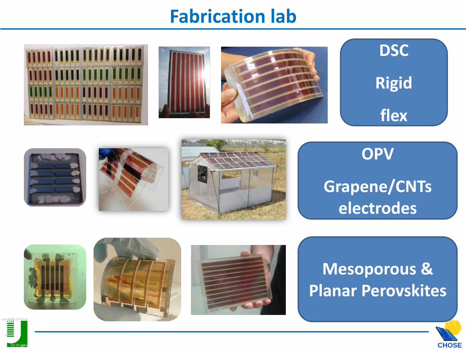
OPV
Grapene/CNTselectrodes
Mesoporous & Planar Perovskites
DSC
Rigid
flex
Fabrication lab

CHOSE
Outline• Background and motivation
• Printing techniques for new generation energy harvesting/storage devices
• The role of substrates: rigid or flexible?
• Examples of printed energy harvesting system: the case of organic and perovskite solar cells
– Working principles
– Role of architectures
– Material engineering for printing processes
– Scaling up to large scale printed devices
– Stability issue
• Examples of printed energy storage system: supercapacitors and batteries
– What is the difference between a supercapacitor and a battery?
– Working principles
– Devices architecture
– Material engineering for printing processes
– Scaling up to large scale printed devices
• How to integrate solar cells and storage systems?
• Conclusions and future perspectives

CHOSE
Background
Sustainable energy supply is of paramount importance to support an expanding worldwith increasing living standards and growing energy needs. On the other hand, in the lastfew years, new generation of portable electronics devices have been enriching ourprofessional and recreational lives to an extent that they have become indispensable foralmost everyone. Flexible and stretchable devices can be used in a wide range ofconsumer applications, ranging from wearable electronics, to mobile healthcare, toInternet of Things (IoT) technology
Smart man

CHOSE
From conventional electronics to printed electronics
• Microelectronics changed the world by enabling many intelligent products
• A new field of electronics is emerging that cannot be made small, but must be big in order to interact with big things
• This is flexible, printed electronics and its most important feature is that it can conform to surfaces to impact a wide range of applications

CHOSE
Printed electronic market
* APAC =Asia Pacific, ROW= Rest of the World
*
https://www.marketsandmarkets.com/Market-Reports/printed-electronics-market-197.html
The overall printed electronics market is estimated to reach USD 13.6 billion by 2023 from USD 6.8 billion in 2018, at a Compound Annual Growth Rate (CAGR) of 14.92% during 2018–2023

CHOSE
Background: A paradigm shift in electronics
Conventional processing Additive/printing processing
Subtractive batch processes (photolithography and wet/dry etching for layer definitions)
Additive continuous processes (printing, laser processing etc.) for layer definitions
Controlled (e.g., a vacuum environment)
Ambient temperature and pressure conditions
Fixed, long production runs of 'same product'
Flexible, short production runs -'flexible' product functionality
Conventional Electronics Organic Electronics

CHOSE
What do we need for Printable Electronics?
Low cost
Large area
Compatible with unconventional
substrates
Stability/
Durability
In air compatible process

CHOSE
Applications

CHOSE
Printing technologies classification 1/2
Printing techniques
Contact printingtechniques
Screen printing Blade coating
Fexographicprinting
Gravure printing
Slot die coating Pad printing
Non-contactprinting
techniques
Laser Direct Writing
Aereosol/Spray coating
Inkjet printing

CHOSE
Printing technology classification 2/2
Roll to roll printing techniques Batch printing techniques

CHOSE
Inks type
Both organic and inorganic inks have been developed for printed electronics

CHOSE
Inks characteristics
The most common types of inks are water, oil or solvents based. The general form of theink consist of a mixture of compounds (pigments or dyes, resins, solvents, fillers,humectant and additives), in liquid or solid state, with specific proprieties adapted to theprinting technology characteristic, such as viscosity, surface tension, etc., to be easilyprinted in a large variety of substrates.
THE INK FORMULATION REQUIRES THE USE OF GREEN AND SUSTAINABLE
MATERIALS, FURTHERMORE HAS, IN SOME SPECIFIC CASES TO BE
ADAPTED TO THE SUBSTRATE WHERE IT HAS TO BE DEPOSITED
• Non halogenated solvents
• Non-toxic and with low volatile organic
compounds (VOC)
• Boiling point ≤ 200°C
• Reduced environmental impact

CHOSE
Printable substratesUnderstanding the printing process and relationships between process parameters andprinting quality (e.g., print resolution, uniformity and electrical conductivity of printedlayer) is necessary for process optimization, as well as the suitability of the selectedmaterial in terms of adhesion and final applications; the appropriateness of the printedtechnology and ink, properties, the process deposition rate, etc. In this context the typesubstrate plays a fundamental role
• Glass is rigid, heavy, typically hydrophobic, but issemitransparent, is a good barrier as encapsulant fororganic materials and can survive to high temperatures
• Metal can be flexible and treated at high temperature islimited on the freedom of design and is high cost
• Polymers composites, such as, glass-reinforced epoxylaminates with flame retardant have been largely used inrigid printed circuit boards (PCB)
• Non-reinforced polymers such as, PET, PEN, PDMS, areflexible, lightweight materials, more economicallyprocessed, can be transparent. Their major drawback lieson the low surface energy, which, normally requires aprior surface treatment before printing and low processingtemperatures.
• Paper, flexible reciclable, lightweight, low cost, compatiblewith most of the inks used for printed electronics. Maindrawback, low processing temperature and durability

CHOSE
Interaction between the ink and the substrate
The transfer and distribution of the ink on a substrate depends on thewettability, spreadability and adhesion capabilities.
Several factors influence the quality of the printed material
• Substrate properties (chemical composition, surface topography and porosity, etc.).
• Conductive ink properties (chemical composition, rheological behavior, the rate of solvent evaporation, etc.).
• The superficial tension (ST) of the ink and the surface energy (SE) of the substrate that will receive the ink, i.e., the difference between them.
• Functional groups and their intermolecular forces present in the ink/polymer system.
Superficial Tension (ST) refers to the amount of cohesive forces between liquid molecules.
The SE describes the degree of energy with which the molecules of the surface of a solid draw and allow adherence of a fluid

CHOSE
Wettability and contact angle
The contact angle measurement allows to evaluate the surface wettability,spreadability and adhesion.
How to increase the wettability?
Inks formulation
Surface treatments
Plasma treatment
Chemical or mechanical induced roughening of the surface
Use of a primer (Silanization for example)

CHOSE
Contact angle: the case of PEDOT:PSS on glass
Poly(3,4-ethylenedioxythiophene)-poly(styrenesulfonate) (PEDOT:PSS) is a printablepolymer commonly used in organic electronics for several application: as conductiveelectrode or hole transporting material in solar cells and OLED, for printed RFID tags,as component for sensor, for RF shielding. It has several formulation, in terms ofadditive used in the solution that allow to change its properties and in general can bepurchased in water based suspensions

CHOSE
Large area coating techniques
PAD-PRINTING
SCREEN-PRINTING
F.C. Krebs / Solar Energy Materials & Solar Cells 93 (2009) 394–412
INK-JET PRINTING
DOCTOR BLADING
SLOT-DIE
SPRAY-COATING
There is a huge amount of film-forming techniques, and each of it can have specific characteristic and can be applied to the realization of printed electronic device
Y. Galagan et al. Adv. Eng. Mater. 2018, 1701190

CHOSE
Lab scale vs high volume processingTypically on lab scale small substrates are used Mostly used techniques are:
spin coating, doctor blading, casting
On large scale, a roll-to-roll coating, in which the substrate can be imagined as a
continuous roll of material on which the different substrates are deposited, is
currently under development.
The ideal process on large area
• Solution processing of all layers on
flexible substrates controlling the film
thickness, uniformity and shape
• Few coating and printing steps, high
speed
• Small amount of materials
• Free from costly indium, toxic solvents
and chemicals
• Low environmental impact and a high
degree of recyclability.
• Low costs

CHOSE
First step
material deposition
Second step (spin-up)
ramp acceleration
Third step
costant rotation speed
(film levelling, solvent
evaporation)
Spin coating
w = rotation speed
K and a = empirical constants that depend
on the physical properties of the solvent
(viscosity, volatility and diffusivity), of the
solute (molecular weight) and of the
concentration of the solute
d = kwa
K. Norrman, A. Ghanbari-Siahkali, N.B. Larsen, Rep. Prog. Chem.
Sect. C 101 (2005) 174–201.
This is a batch deposition technique, used typically in lab to test new materials for severaltype of printable devices (solar cells, photodetectors, OLED, OTFT, sensors

CHOSE
Advantages:
• Highly reproducible films homogeneous on large area (max dim.
1,5m x 1,5)
• Well established coating technique
Disadvantages:
• High waste of materials
• Serial technique for which each substrate have to be handled
separately
• No patterning allowed
Good on lab scale to optimize devices and materials
Spin coating

CHOSE
Blade Coating
The doctor blade technique is widely used in laboratory fabrication due to its
simplicity.This process relies on a coating being applied to the substrate
which then passes through a 'gap' between a moving or fixed 'knife' and a
fixed or moving support. As the coating and substrate pass through, the
excess is scraped off. This process can be used for high viscosity coatings
and very high coat weights. There are innumerable variants of the relatively
simple process which is rugged, hard-working and somewhat inaccurate.

CHOSE
Doctor blading
F.C. Krebs / Solar Energy Materials & Solar Cells 93 (2009) 394–412
The final thickness of film depends on:
•The gap between the blade and the
film
• The concentration of the solid
material, density of the material
• Surface energy
• Surface tension of the coating
solution
• Meniscus formed between the blade
and the wet film
cgd
2
1
g= gap distance
c= concentration of the solid material
=density of the material in the final film

CHOSE
Advantages:
• Simple technique
• Less waste of material respect to spin coating (< 5%)
•No degradation of the multilayer organisation occurs with successive
depositions
• Possible application to R2R process in his knife over edge configuration
Disadvantages:
• Slow technique
• Problems with the crystallization of the material during the deposition
• No patterning allowed
Doctor blading

CHOSE
Blade Coating

CHOSE
Screen Printing
Step 1 - Preparing the screen
A fine fabric mesh is coated with a photosensitive emulsion. The mesh is stretched over a frame.
Step 2 - Creating the stencil
The positive films are laid directly on top of the mesh. Ultraviolet light is shown onto the assembly. Where
there is an image on the positive film, no light gets through to the emulsion on the screening assembly
beneath, leaving it unexposed. Where the film is clear, the light passes through and hits the emulsion, causing
it to harden. When the development process is complete, the unexposed, soft areas of emulsion are washed
away, leaving only the porous fabric mesh.
Step 3 - Printing
The stencil is placed directly on top of the item that will receive the ink. Ink is poured on top of the stencil,
and a squeegee is scraped over the top, forcing ink through the image area of the stencil, and onto the
printable surface.
Step 4 - Drying
It is typical that the ink will be cured thermally or with ultraviolet light, so that subsequent layers can be
applied without difficulty, and so that printed items can be stacked on top of each other immediately.

CHOSE
F.C. Krebs / Solar Energy Materials & Solar Cells 93 (2009) 394–412
ckVd pscreen
Vscreen=theoretical paste
volume of the screen
kp= pick-out ratio
c=concentration of the solid
material
=density of the material in
the final film
Parameters:
Ink:
High Viscosity
Surface tension
Low volatility
Squeegee:
Hardness
Speed
Pressure
Screen:
Nominal thread diameter
Mesh count
Open area
Film thickness
Screen Printing

CHOSE
Advantages:
• Applicable for any soluble or dispersible polymer
• Smooth areas possible (<5 nm deviation)
• Large areas possible (up to 1 m2)
• Low cost equipment
• Proceeds at ambient temperatures
• Almost no loss of material during the deposition
Disadvantages
• Batch operated (semi-continuous process )
• Screens have to be cleaned often
• Ink on the screen can pick up contamination
• Many parameters for tuning layer thickness and smoothness
Screen Printing

CHOSE
Screen Printing

CHOSE
Slot-die CoatingThe slot-die coating is a contact printing technique where the slot head allows,
thanks to the specific design of the internal mask, the deposition of patterns with
several line dimension.
d= thickness (cm),
f= flowrate (cm3 min-1),
S=web speed (cm min-1)
w= coated width (cm)
c= solid content in the inking (cm-3)
R=density of the dried ink material (g cm-3)

CHOSE
Slot-die CoatingAdvantages:
• Applicable for any soluble or dispersible polymer with low
viscosity
• Smooth areas possible (<5 nm deviation)
• Large areas possible (up to 1 m2)
• Proceeds at ambient temperatures
• Almost no loss of material during the deposition
• Thicknesses up to 50 microns
• Easy in changing the pattern
Disadvantages
• Design of the head is very complex
• Meniscus has to be controlled very carefully
• Many parameters for tuning layer thickness and smoothness
CHOSE
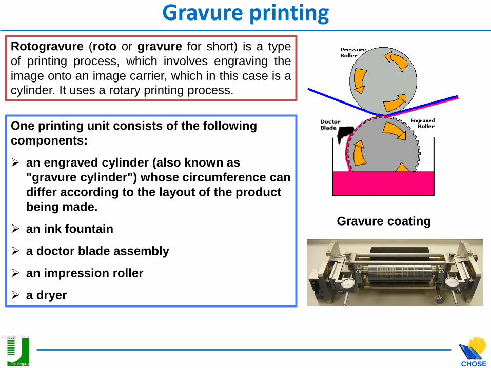
Gravure printing
Gravure coating
Rotogravure (roto or gravure for short) is a type
of printing process, which involves engraving the
image onto an image carrier, which in this case is a
cylinder. It uses a rotary printing process.
One printing unit consists of the following
components:
an engraved cylinder (also known as
"gravure cylinder") whose circumference can
differ according to the layout of the product
being made.
an ink fountain
a doctor blade assembly
an impression roller
a dryer

CHOSE
Gravure printing
Gravure coating
Advantages:
printing cylinders that can last through large-
volume runs without the image degrading
good quality image reproduction
low per-unit costs running high volume
production
Disadvantages
high start-up costs: hundreds of thousands
of copies needed to make it profitable
rasterized lines and texts
long lead time for cylinder preparation,
which is offsite as the techniques used are
so specialized

CHOSE
Inkjet printing
Inkjet printing
cVNd dd
Nd= Number of droplets
Vd= Droplets volume
c=concentration of the solid
material
=density of the material in
the final film
S. Sumaiya et al. Technologies 2017, 5, 53; doi:10.3390/technologies5030053

CHOSE
Inkjet printing
S. Sumaiya et al. Technologies 2017, 5, 53; doi:10.3390/technologies5030053

CHOSE
Spray-coating technique
ADVANTAGES
• Solution processing Low-cost deposition
• Large Area deposition suitable also for flexible substrates
with different morphologies
• Fluid waste reduced respect to spin-coating
• Easy to use
ISSUES
• Film control thickness, uniformity and roughness
• Many process-variables to be controlled
Commercial Airbrush

CHOSE
Spray-Coating parametersInstrument variables
N2 Flow
Polymer
Ink
Hot Plate
Distance
Dual
Action
Lever
Air Pressure(P) : Air pressure inside the nozzle
Velocity(V) : speed of nozzle X Y movements
T=30°c : Substrate temperature
d : Distance between Spray nozzle and substrate
Nozzle Aperture(AP): Nozzle opening radius
Flow rate (FR): Flow rate of solution

CHOSE
AtomizationFor low-viscosity liquids, the deformation of the drop is primarily determined by the Weber number (We), a dimensionless parameter representing the ratio of the aerodynamic forces and the stabilizing surface tension:
𝑊𝑒 = (𝜌𝑉2𝐷 Τ) 𝜎
where ρ is the gas density (kg/m3), V is the initial relative velocity between the gas and
the liquid (m/s), D is the initial diameter of the drop (m) and σ is the surface tension of
the drop (N/m). The higher the Weber number, the larger are the deforming external
pressures forces (resulting in droplet breakup) compared with the reforming surface
tension forces, aiming at droplet aggregation.
- Bag 12<We<100
- Stripping (or shear) 100<We<350
- Catastrophic We>350

CHOSE
Drop impact

CHOSE
Drop impact
The parameters that affect the outcome of the drop are listed in Table: in addition to
the impact velocity (V), the drop size (D), the surface tension (σ) and the viscosity (µ)
included in Weber and Ohnesorge numbers, the surface roughness and wettability are
also considered through the roughness amplitude (Ra), the roughness wavelength (Rw)
and the receding contact angle (Ɵrec).

CHOSE
PEDOT:PSS Spray coating
Variable Parameters: PRESSURE Variable Parameters: dilution, time of spray
Before
After
Distancenozzle/substrate: 16 cm Distance
nozzle/substrate: 13 cm
Variable Parameters: distance from substrate
Final deposition of PH1000 on CPP

CHOSE
Large area spray coating
CHOSE
Comparison of the deposition techniques
F.C. Krebs / Solar Energy Materials & Solar Cells 93 (2009) 394–412

CHOSE
Example 1: Printable solar cellsand modules

CHOSE
Application: Solar cell realization

CHOSE
Solution processed Photovoltaic
OPV -OPVius Expo Milan 2015
DSSC Façade System
at EPFL SOLARONIX
OPV – CSEM Brasil 2016
Saule- Flexible Perovskite solar module
CHOSE
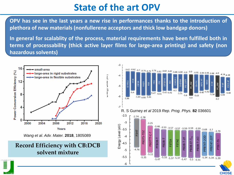
State of the art OPV
R. S Gurney et al 2019 Rep. Prog. Phys. 82 036601
Wang et al. Adv. Mater. 2018, 1805089
OPV has see in the last years a new rise in performances thanks to the introduction ofplethora of new materials (nonfullerene acceptors and thick low bandgap donors)
In general for scalablity of the process, material requirements have been fulfilled both interms of processability (thick active layer films for large-area printing) and safety (nonhazardous solvents)
Record Efficiency with CB:DCB solvent mixture

CHOSE
Single-layer device
Problem: insufficient photon-current conversion (efficiency ~ 0,1%)
a) polymers are amorphous
“hopping” transport
low mobility
b) strong electrostatic interactions
strong exciton bound
high dissociation energies
c) exciton diffusion length ~10nm, but dissociation occurs at the interfaces (too far!)
Single-layer
–
+
hν
eVTransparent electrode
Semiconductor polymer
Metal electrode (opaque)
Optical source

CHOSE
Single layer organic devices
• Organic films between asymmetric contacts
• Light generates excitons, charge separation by exciton dissociation at interfaces
• Exciton diffusion length 1-10 nm, absorption depth >100 nm
• Photocurrent limited by exciton diffusion length
• Power efficiency < 0.1%

CHOSE
Bi-layer device (heterojunction)
Use of two polymers, donor and acceptor (p and n type) better conversion efficiency (~1%)
photon absorption and exciton formation next to interface
exciton dissociation favored by energetic levels
Remaining problems:
? higher series resistance
? solvent-crossing
Double-layer
Transparent electrode
Donor polymer (p)
Metal electrode
Acceptor polymer (n)
–
+
hν
Optical source
eV

CHOSE
Bulk-Heterojunction (BHJ) Device
Photo-Voltaic effect in organic heterojunction:1) Photon absorption2) Exciton formation3) Exciton diffusion to heterojunction a-d (acceptor-
donor)
4) Exciton dissociation (electrons “hop” from
LUMOdonor to LUMOacceptor)5) Carriers transport towards electrodes6) Harvesting of carriers at electrodes
P3HT
[60]PCBM
trasperent anode
polymer blend (BHJ)
metal cathode
light source
polymer
(donor)
fullerene
(acceptor)
P3HT
[60]PCBMheterojunction a-d

CHOSE
How get OPV with good preformances?

CHOSE
Morphology
a,b) Schematic pictures showing the microscopic
process during annealing. c) Grazing incidence X-
ray spectrum on a blend before and after
annealing, showing the evolution of the a-axis
oriented P3HT crystals.
Dennler et al., Adv. Mater., 2009, 21, 1–16
Effect of the thermal annealing on the
phase separation
TEM images of 1:1 blend of P3HT and
PCBM prior (a) and after (b) thermal
annealing at 150°C for 30 minutes (scale
bar 0.5 mm).
Thomson et al., Angew. Chem. Int. Ed., 2008, 47, 58–77

CHOSE
Effects of morphology
Room-temperature electron () and hole (ο)
zero-field mobilities in (1:1) blends of
P3HT:PCBM as a function of postproduction
annealing temperature of the completed
devices. For comparison, the hole mobility
measured in pristine P3HT devices (Δ) is also
shown.
Mihailetchi et al., Adv. Funct. Mater., 2006, 16, 699
Absorption spectra of P3HT:PCBM blend
films for different annealing temperatures.
Mihailetchi et al., Adv. Funct. Mater., 2006, 16, 699

CHOSE
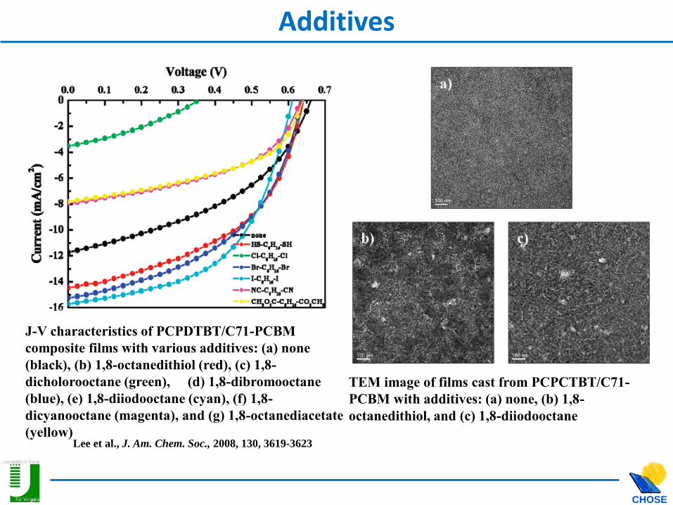
Additives
Lee et al., J. Am. Chem. Soc., 2008, 130, 3619-3623
CHOSE
Additives
Lee et al., J. Am. Chem. Soc., 2008, 130, 3619-3623
J-V characteristics of PCPDTBT/C71-PCBM
composite films with various additives: (a) none
(black), (b) 1,8-octanedithiol (red), (c) 1,8-
dicholorooctane (green), (d) 1,8-dibromooctane
(blue), (e) 1,8-diiodooctane (cyan), (f) 1,8-
dicyanooctane (magenta), and (g) 1,8-octanediacetate
(yellow)
TEM image of films cast from PCPCTBT/C71-
PCBM with additives: (a) none, (b) 1,8-
octanedithiol, and (c) 1,8-diiodooctane

CHOSE
Ink preparation for AN INDUSTRY COMPATIBLE PROCESS
GREEN MATERIALS & SUSTAINABILITY
• Non halogenated solvents
• Non-toxic and with low volatile
organic compounds (VOC)
• Boiling point ≤ 200°C
• Reduced environmental
impact
S. Zhang et al. Materials Today Volume 19, Number 9 November 2016

CHOSE
Solvent typically used for OPV solution preparation
S. Zhang et al. Materials Today Volume 19, Number 9 November 2016

CHOSE
How to change materials towards the use of green solvents?
S. Zhang et al. Materials Today Volume 19, Number 9 November 2016

CHOSE
Ink preparation: role of solvent
Boiling points: MS = 165°C / AP = 202°C
• δD Dispersive interaction
• δp Intermolecular dipole interaction
• δH Hydrogen bond interaction
C.Park et al., Organic Electronics, Vol, 12, Issue 9, September 2011, Pages 1465-1470
The choiche of the proper solvent can be done using the Hansen solubility parameters(HSP), which describe the total cohesion energy, E by three contributions: the dispersioninteractions, Ed, permanent dipolepermanent dipole molecular interactions, Ep, and thehydrogen bonding molecular interactions, Eh.
δ=(E/V)1/2

CHOSE
Ink preparation: The role of molecular weight
P3HT high molecularweight (60-75k)P3HT:PCB60M
P3HT low molecular weight(21k)P3HT:PCB60M
ORTHO PARA
P3HT high molecularweight (60-75k) in o-DCB:CB
P3HT:PCB60MSPIN DCB:CB
40°
Voc (mV) Jsc
(mA/cm2)
FF (%) Eff (%)
Inverted
structure
510 7.8 45 1.8
Direct
structure
546 9.4 49 2.5
P3HT(Poly(3-hexylthiophene-2,5-diyl): PCBM ([6,6]-phenyl-C61-butyric acid methyl ester) with non- halogenated solvent (Xylenes)
G. Susanna et al., Solar Energy Materials & Solar Cells 95 (2011) 1775–1778
M-Koppe et al ,Macromolecules, 2009, 42 (13), pp 4661–4666

CHOSE
Water based OPV
Low efficiency η= 0.7 %

CHOSE
Example of printing techniques appliedto OPV: spray coating

CHOSE
η ~4,1%
FF 59%
Dep Amb Tk (nm) Voc [V]Jsc
[mA/cm2]
FF
[%]η [%]
SpinN2
200 0.6311.96 55 5.1
Air
9.97 53 3.3
Spray
135 0.66 8.89 60 3.6
2000.64
10.34 57 3.8
270 10.98 59 4.1
340 0.61 10.62 50 3.2
G. Susanna et al., Solar Energy Materials & Solar Cells 95 (2011) 1775–1778
Co-Solvent optimization: morphology tuning
Spin DCBSpray DCB:CB
40°
Spray DCB:CB
70°
Spray DCB:CB
50°
Spray DCB:CB
25°
Spray DCB
DCB: improves the phase separation
CB: allows better spray deposition
Co-solvent mixture: DCB:CB (1:5)

CHOSE
BHJ-SC with non-Chlorinated solvents
Susanna et al. Solar EnergyMaterials&SolarCells134(2015)194–198
PCBM
polymer
(donor)
fullerene derivative
(acceptor)
PTB7
The introduction of non-chlorinated solventsplays a fundamental role in the direction of
large area device realization

CHOSE
Fully spray coated module
https://nanohub.org
PTB7:PCBM sprayed active layer
ALUMINIUM opaque
PEDOT:PSS
HWF electrode
Glass substrate
Electron transporting layer (ETL)
PHOTO-ACTIVE LAYER
Hole transporting layer (HTL)
Anode
Cathode
HOLE TRANSPORTING LAYER & TOPELECTRODE
ELECTRON TRANSPORTING LAYER
1° INTERFACE: ELECTRON TRANSPORTING LAYERLAYER
PHOTO-ACTIVE LAYER
ZnOITO
PEIE
• Work Function reduction
• Lower energy barrier for charge transportPAL/ETL
• Avoid electron trapping and high seriesresistance
• Charge acceleration transfer
• Reduction of recombination at interface
PEDOT:PSS
PHOTO-ACTIVE layer
HWF electrode
MoO3 evaporated
Ag evaporated
SMALL AREA DEVICE 0.1 cm2
CHOSE
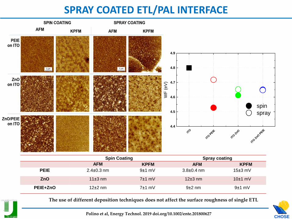
SPRAY COATED ETL/PAL INTERFACE
Polino et al, Energy Technol. 2019 doi.org/10.1002/ente.201800627
ITO
ITO P
EIE
ITO Z
nO
ITO Z
nO P
EIE
4.4
4.5
4.6
4.7
4.8
4.9
spin
spray
WF
(e
V)
The use of different deposition techniques does not affect the surface roughness of single ETL
Spin Coating Spray coating
AFM KPFM AFM KPFM
PEIE 2.4±0.3 nm 9±1 mV 3.8±0.4 nm 15±3 mV
ZnO 11±3 nm 7±1 mV 12±3 nm 10±1 mV
PEIE+ZnO 12±2 nm 7±1 mV 9±2 nm 9±1 mV

CHOSE
SPRAY COATED ETL/PAL INTERFACE
Polino et al, Energy Technol. 2019 doi.org/10.1002/ente.201800627
ZnO/PEIE PAL Voc (mV) Jsc
(mA/cm2)
FF(%) Eff(%)
Spray Spray 0.68±0.30 13.7±0.20 54±0.07 5.5±0.01Spin Spin 0.70±0.01 14±0.08 67±0.08 6.6±0.40spray Spin 0.70±0.02 13±0.07 65±0.08 6.0±0.06

CHOSE
https://nanohub.org
SPRAY COATED HTL/PAL INTERFACE
2° INTERFACE: HOLE TRANSPORTING LAYER & ANODE
ZnOITO
PEIE
PEDOT:PSS
PHOTO-ACTIVE layer
HWF electrode
HTL
PEDOT:PSS
PEDOT:PSS
PH1000 PEDOT:PSS vs. ANHYDROUS PEDOT (A-PEDOT)
PH1000 ON PTB7 A-PEDOT ON PTB7
Rs (Ω∕) T550(%) δ dc/δ op
ITO 8 85.5 289
A-PEDOT (REF) 20 40 16.2
CPP:PH1000 26 40 12.4
CPP : A-PEDOT 37 66.9 22.9
Polino et al, Energy Technol. 2019 doi.org/10.1002/ente.201800627
Voc
(mV)
Jsc (mA/cm2) FF
(%)
Eff
(%)
CPP:PH1000 0.69 8.60 28.2 1.7
CPP:A-PEDOT 0.68 15.6 33.8 3.6CPP:A-PEDOT (ILL.PEDOT)
0.64 9.55 33.2 2.0

CHOSE
FROM SMALL TO LARGE AREA
The module is composed of 4 series-connected solar cells
Active area
7mm x 49mm x 4 = 13.7cm2
Laser patterned ITO
substrate Mask to deposit
ETL/BLEND/HTL
Mask to deposit
HTL/ANODEP1 P2 P3

CHOSE
FULL SPRAY MODULES
Voc (V) Jsc (mA/cm2) FF (%) Eff (%)
MoO3 Ag evap 2.8 3.0 37.2 3.0
V2O5/ A-PEDOT 2.5 1.1 30.6 0.8
-0.5 0.0 0.5 1.0 1.5 2.0 2.5 3.0
-3.36-3.15-2.94-2.73-2.52-2.31-2.10-1.89-1.68-1.47-1.26-1.05-0.84-0.63-0.42-0.210.000.210.42
Voltage (V)
Cu
rre
nt
De
ns
ity
(m
A/c
m2
)
13 cm2 active area
3-Layers spray coated
Full spray

CHOSE
FULL SPRAY MODULES AT WORK!

CHOSE
Devices on flexible substrates
Semi-trasparent Flexible

CHOSE
Completely inkjet printed OSC
T.M Eggenhuisen et al, J. Mater. Chem. A, 3, (2015)
All-inkjet printed large area (>1 cm2) organic
solar cells with power conversion efficiency of
4.1% deposited from environmentally friendly
solvents in an air atmosphere.
The semitransparent front and back electrodes
consist of PEDOT:PSS and conductive Ag
fingers, avoiding the use of ITO.

CHOSE
Fully printed OPV
Y. Galagan et al. Adv. Eng. Mater. 2018, 1701190

CHOSE
Large area Modules
Techniques used:
Screen printing
Blade coating
Slot-die coating
Maximum efficiency on the modulewith low bandgap polymers: 5%
HOPV conference, Rome, May 2019

CHOSE
Perovskite Solar cellsPSC

CHOSE
Organometal trihalide Perovskite
Methylammonium lead halide perovskite
A=CH3NH3(+) ; B= Pb(+); Sn X= I(-), Cl(-), Br(-)
CH3NH3PbI3
Baikie et al. J. Mater. Chem. A, 2013, 1, 5628, G. Eperon et al Energy Environ. Sci., 2014,7, 982-988, P. Gau et al, Energy Environ. Sci., 2014,7, 2448-2463
Direct band gap of 1.51 eV for CH3NH3PbI3
ABX
Solution process
MethylAmmonium Lead (Pt) Iodite (MAPI) Good hole and electron conductor, Diffusion length from 100 nm to 1 μm
By the insertion of Br atoms (x) on the perovskite crystalline structure, or using adifferent organic molecule the energy gap can be varied.

CHOSE
Mesostructured vs Planar Perovskite Solar cells
Y. Zhang, et al. Materials Horizons, 2015, 2, 315-322
Easier perovskite grown
Better charge transport
Less production step
No sintering step
Mesostructured
(DSC like)
Planar
(OPV like)

CHOSE
Several deposition methods
Spin coating perovskite Drying RT Annealing 90-130°C
1) One-step procedure
PbI2 depositionCH3NH3I addition
Perovskite layer
2) Two-step procedure
1a) 3 CH3NH3I + PbCl2 → CH3NH3PbI3-xClx + …
CH3NH3I + Pbl2 → CH3NH3PbI31b) Solvent engineering
3) Vapor deposition
S. Casaluci,et al. Journal of Power Sources 297, 504 (2015)

CHOSE
Key issue for PSK ink formulation
Li et al. (2018) DOI: 10.1039/c8ta04120b

CHOSE
From cells to Modules
1 cm2
10 cm2
100 cm2
?

CHOSE
Perovskite module: Monolithic integration
BL-TiO2
PerovskiteHTL
TiO2/Perovskite
FTO
GLASS
Au
Scribing of the FTO.
Easy: laser (CO2 etc.)
Patterning of C-TiO2, Perovskite
and HTM. Very critical

CHOSE
Au/FTO: Influence on the I-V characteristics
TLM meas. Lt [mm] RC [Ω]
Au/BL-TiO2/FTO 3.6 2.607
Au/FTO 0.7 0.091
BL
BL
F. Matteocci et al. Prog. Photovoltaics 24, (2016) 436

CHOSE
Laser Patterning Procedures (LPP)
CO2 Laser
(l=10µm) Au deposition
Nd:YVO4 Laser
(l=532nm)
Au deposition
LPPPEROVSKITE
nc-TiO2
FTOBL-TiO2
Perovskite
LPPP3HT
CO2
LaserP3HT
LPPPEROVSKITE/P3HT
nc-TiO2
FTOBL-TiO2
Perovskite
P3HT
F. Matteocci et al. Prog. Photovoltaics 24, (2016) 436

CHOSE
Optimization of the laser patterning
FF=78%
FF=55%
Module number Layer Patterning VOC [V] JSC [mA/cm2] FF (%) PCE (%)
Modules 1-2PEROVSKITE CO2 LASER
3.27 -11.6 55.4 5.3 P3HT Chemical Etch
Modules 3-4PEROVSKITE CO2 LASER
3.34 -12.1 66.1 6.7 P3HT CO2 LASER
Modules 5-6PEROVSKITE
P3HTNd:YVO4 LASER 3.36 -13.4 77.8 8.2
CO2
Laser patterning
10.1 cm2 active area
Nd:YVO4
Laser patterning
F. Matteocci et al. Prog. Photovoltaics 24, (2016) 436

CHOSE
Spiro-OMeTAD Modules: one vs two step
Eff= 13%, 10.1 cm2
Very limited hysteresis effect
𝐽𝑅𝑆 ෨𝑉 − 𝐽𝐹𝑆 ෨𝑉
𝐽𝑅𝑆 ෨𝑉= 0.065
෨𝑉 = 0.8𝑉𝑂𝐶scan rate: 0.15V/s
(aa)
F. Matteocci et al. Prog. Photovoltaics 24, (2016) 436

CHOSE
From modules to MODULES
10 x
10 cm2
100 cm2
?

CHOSE
From spin coating to air-assited blade coating
SPIN 10 M. SPIN 30 M. BLADE 10 M. BLADE 30 M.0.0
0.2
0.4
0.6
0.8
1.0
1.2
Vo
c (
mV
)
SPIN 10 M. SPIN 30 M. BLADE 10 M. BLADE 30 M.0
5
10
15
20
Js
c (
mA
/cm
2)
SPIN 10 M. SPIN 30 M. BLADE 10 M. BLADE 30 M.0
2
4
6
8
10
12
14
PC
E (
%)
SPIN 10 M. SPIN 30 M. BLADE 10 M. BLADE 30 M.0
20
40
60
80
FF
(%
)
0.0 0.2 0.4 0.6 0.8 1.0 1.2
-20
-15
-10
-5
0
Jsc (
mA
/cm
2)
Tensione (V)
J (3.3 - Blade)
J (2.3 - Spin)
Blade 13.3%
Spin 12.1%
A new high performing air-assisted blade coating technique for perovskite printing
Two-step deposition
Small area
Glass
air
blade
PbI2
S. Razza et al. J. Power sources 277, 286 (2015)

CHOSE
Scaling-up of perovskite modules (100 cm2)
S. Razza et al. J. Power sources 277, 286 (2015)
Optimized blade coating deposition

CHOSE
Large area PSK modules
Palma et al., IEEE Journal of Photovoltaics, 2017, 10.1109/JPHOTOV.2017.2732223

CHOSE
Non Chlorinated solvent for HTM
F.Isabelli et al. ACS applied energy Materials, 10.1021/acsaem.8b01122
Commonly used as HTM for PSC, diluited in Chlorobenzene which isnot suitable for scalable process

CHOSE
Non Chlorinated solvent for HTM
F.Isabelli et al. ACS applied energy Materials, 10.1021/acsaem.8b01122

CHOSE
Non Chlorinated solvent for HTM
F.Isabelli et al. ACS applied energy Materials, 10.1021/acsaem.8b01122
Optical microscope images of spiro-
OMeTAD layer deposited from
different solvents: (A) chlorobenzene,
(B) anisole, (C) phenetole, (D) o-xylene, (E) p-xylene, and (F) toluene
A) Spin coating with
different
postannealing
temperatures after
the deposition of
spiro-OMeTAD and
B) Doctor blading
CHOSE
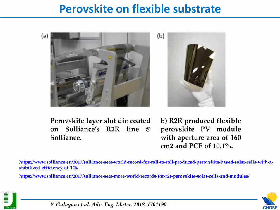
Perovskite on flexible substrate
https://www.solliance.eu/2017/solliance-sets-world-record-for-roll-to-roll-produced-perovskite-based-solar-cells-with-a-stabilized-efficiency-of-126/
https://www.solliance.eu/2017/solliance-sets-more-world-records-for-r2r-perovskite-solar-cells-and-modules/
Perovskite layer slot die coatedon Solliance’s R2R line @Solliance.
b) R2R produced flexibleperovskite PV modulewith aperture area of 160cm2 and PCE of 10.1%.
Y. Galagan et al. Adv. Eng. Mater. 2018, 1701190

CHOSE
PSC on unconventional substrates: Paper
First perovskite
solar cell on paper
State of the art efficiency
(2.7%) for cell on paper
S. Castro et al, IEEE EDL, 2017

CHOSE
Example 2: Energy storage

CHOSE
Energy storage: several possibilities
CAES = Compressed Air Energy Storage; LAES = Liquid Air Energy Storage; SNG = Synthetic Natural Gas

CHOSE
Which type of storage?

CHOSE
Pros and Cons

CHOSE
Electrochemical and chemical energy storage devices
Supercapacitor
J. Xie et al, Journal of Power Sources 401 (2018)

CHOSE
How do they work?
Solid or liquid electrolyte
Electroactive materialElectrode
Activatedcarbon
Separator
Supercapacitor Battery
+ -
Energy storage mechanism and the similar device
configuration/characterization techniques cause
confusions.
• Batteries: rapid surface-controlled electrochemical
reactions
• Supercapacitors: stores energy in the crystal lattices or
porous materials through much slower electrochemical
reactions with limits from the phase transformation,
chemical binding changes or/and reactant diffusions.
J. Xie et al, Journal of Power Sources 401 (2018)

CHOSE
Power vs Energy
J. Xie et al, Journal of Power Sources 401 (2018)

CHOSE
Electric double layer supercapacitors
• EDLCs are supercapacitors that employelectrostatic charge separation only.
• The energy storage process of EDLCs takes placeat the interface between the electrode surface andthe electrolyte
• The electrostatic charge transfer is fullyreversible, which results in efficient devices witha long life-time
• The separator is ion permeable and also preventsshort circuits between the electrodes.
• The space between the electrodes is filled withelectrolyte.
• By charging the device, two layers of oppositecharge are formed at the interface between theelectrode and the electrolyte,

CHOSE
Which printing techniques for Supercaps?
Zang et al. Chem. Soc. Rev., 2019, 48, 3229--3264

CHOSE
Possible supercap architectures
Vertical /sandwich
Planar
Zang et al. Chem. Soc. Rev., 2019, 48, 3229--3264

CHOSE
Which substrate?
Zang et al. Chem. Soc. Rev., 2019, 48, 3229--3264

CHOSE
Example of screen printed supercap
• Simmetric planar supercap
• Electrodes: RuO2/PEDOT:PSS/ graphene
• Electrolyte: 1 M H2SO4
• A specific capacitance of 820 F g-1
• Asimmetric planar supercap
• Electrodes: reduced GO
• Electrolyte: H2SO4 PVA gel electrolyte
• Aereal capacitance of 2.5 mF cm-2
S. Cho, M. Kim and J. Jang, ACS Appl. Mater. Interfaces, 2015, 7, 10213–10227, A. M. Abdelkader, N. Karim, C. Valles, S. Afroj, K. S. Novoselov
and S. G. Yeates, 2D Mater., 2017, 4, 035016

CHOSE
3D printed supercap
• Asimmetric planar supercap
• Electrodes: V2O5/GO//G-VNQDs/GO
• Electrolyte: PVA/LiCl
• A potential window of 1.6 V, an areal capacitance, of 207.9 mF cm-2, an areal energy density of 73.9 mW h cm-2
• Asimmetric planar supercap
• Electrodes: V2O5/GO//G-VNQDs/GO
• Electrolyte: PVA/LiCl
• A potential window of 1.6 V, an areal capacitance, of 207.9 mF cm-2, an areal energy density of 73.9 mW h cm-2
CHOSE
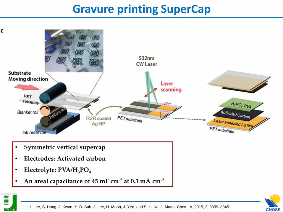
Gravure printing SuperCap
• Symmetric vertical supercap
• Electrodes: Activated carbon
• Electrolyte: PVA/H3PO4
• An areal capacitance of 45 mF cm-2 at 0.3 mA cm-2
H. Lee, S. Hong, J. Kwon, Y. D. Suh, J. Lee, H. Moon, J. Yeo, and S. H. Ko, J. Mater. Chem. A, 2015, 3, 8339–8345

CHOSE
Supercap applications

CHOSE
Integration PV and SC
L. Manjakkal et al.Nano Energy 51 (2018) 604–612, Dong et al. Nano Energy Volume 42, December 2017, Pages 181-186, Liu et al. ACS Appl. Mater. Interfaces201792722361-22368

CHOSE
Acknowledgement
www.chose.it
EU Graphene Flagship Contract n. 604391
People from CHOSE
A.Di CarloA.RealeT.M.BrownG.PolinoF.De RossiG.Susanna
L.La NotteA.AgrestiS.PescetelliF.MatteocciB.TaheriL.Cinà