Stretchable, adhesive and ultra-conformable elastomer thin ...
Full Terms & Conditions of access and use can be found athttp://www.tandfonline.com/action/journalInformation?journalCode=tadr20
Download by: [University of Glasgow] Date: 11 November 2015, At: 04:04
Advanced Robotics
ISSN: 0169-1864 (Print) 1568-5535 (Online) Journal homepage: http://www.tandfonline.com/loi/tadr20
New materials and advances in making electronicskin for interactive robots
N. Yogeswaran, W. Dang, W.T. Navaraj, D. Shakthivel, S. Khan, E.O. Polat, S.Gupta, H. Heidari, M. Kaboli, L. Lorenzelli, G. Cheng & R. Dahiya
To cite this article: N. Yogeswaran, W. Dang, W.T. Navaraj, D. Shakthivel, S. Khan, E.O. Polat,S. Gupta, H. Heidari, M. Kaboli, L. Lorenzelli, G. Cheng & R. Dahiya (2015) New materialsand advances in making electronic skin for interactive robots, Advanced Robotics, 29:21,1359-1373, DOI: 10.1080/01691864.2015.1095653
To link to this article: http://dx.doi.org/10.1080/01691864.2015.1095653
© 2015 Taylor & Francis and The RoboticsSociety of Japan
Published online: 05 Nov 2015.
Submit your article to this journal Article views: 22
View related articles View Crossmark data
Citing articles: 1 View citing articles

Advanced Robotics, 2015Vol. 29, No. 21, 1359–1373, http://dx.doi.org/10.1080/01691864.2015.1095653
SURVEY PAPER
New materials and advances in making electronic skin for interactive robots
N. Yogeswarana,b, W. Danga,b, W.T. Navaraja, D. Shakthivela, S. Khanb, E.O. Polata, S. Guptaa,b, H. Heidaria, M. Kabolic,L. Lorenzellib, G. Chengc and R. Dahiyaa∗
aElectronics and Nanoscale Engineering Division, University of Glasgow, Glasgow G12 8QQ, UK; bCenter for Materials andMicrosystems, Fondazione Bruno Kessler, Trento 38123, Italy; cInstitute for Cognitive Systems, Technical University of Munich,
80333 München, Germany
(Received 11 August 2015; revised 14 September 2015; accepted 15 September 2015)
Flexible electronics has huge potential to bring revolution in robotics and prosthetics as well as to bring about the nextbig evolution in electronics industry. In robotics and related applications, it is expected to revolutionise the way withwhich machines interact with humans, real-world objects and the environment. For example, the conformable electronicor tactile skin on robot’s body, enabled by advances in flexible electronics, will allow safe robotic interaction duringphysical contact of robot with various objects. Developing a conformable, bendable and stretchable electronic systemrequires distributing electronics over large non-planar surfaces and movable components. The current research focus inthis direction is marked by the use of novel materials or by the smart engineering of the traditional materials to developnew sensors, electronics on substrates that can be wrapped around curved surfaces. Attempts are being made to achieveflexibility/stretchability in e-skin while retaining a reliable operation. This review provides insight into various materialsthat have been used in the development of flexible electronics primarily for e-skin applications.
Keywords: electronic skin; novel materials; tactile sensing; robotics
1. Introduction
The rapid advancement in technology in the last few decadeshas now enabled development of robots which has longbeen a mere concept in science fiction movies. From itsprimitive stage as controlled industrial tool operating hu-man restricted environment, robots have evolved into au-tonomous and self-adapting systems to variant situations.Furthermore, robots such as humanoids are expected to beinvolved in day to day human interaction, therefore it isalso critical to build a safer system which can interact withhuman. One possible approach of building such system isby inducing the sense of touch to robots.[1]
Among various human senses, sense of touch plays acrucial role in the way in which we perceive our environ-ment. For instance, information such as surface roughness,temperature and size which are critical for object discrim-ination and manipulation can only be determined by thesense of touch.[2] Inspired from human skin, the develop-ment of artificial skin (also referred to as synthetic skin orelectronic skin (e-skin)) has become an area of immenseinterest to scientists. The primary function of e-skin is toprovide tactile information which could be used to evalu-ate aforementioned parameters for the object handling. Inaddition, tactile sensors can also provide information on
∗Corresponding author. Email: [email protected]
surface compliance, hardness of object and electrical con-ductivities. [3–5] Other possible functionality which couldbe embraced by e-skin are chemical, temperature and bio-logical sensors. Furthermore, development of self-healingmaterials are currently under investigation.[6]
In addition to development of sensors, integration ofsensors over a large area is also a critical requirement forthe development of efficient e-skin. Furthermore, distribu-tion of sensors over non-uniform (or curvy) surface wouldprovide an improved performance due to higher distribu-tion of sensors.[7] In addition to robotics, e-skin can alsohave an influence in applications such as personal healthcare monitoring,[8] wearable technology,[9] artificial intel-ligence and medical prosthetics.[10]
This paper presents an overview of various material usedin the development of e-skin which is critical componentsin tactile sensing. However, unlike in previous review intactile sensing, we have primarily focused on the materialsused for the development of e-skin sensors.[2,11]
2. Tactile sensing for humanoids
Tactile sensing for robots has been studied since 1980s. Inthe context of humanoids, tactile sensing is primarily used
© 2015 Taylor & Francis and The Robotics Society of Japan
Dow
nloa
ded
by [
Uni
vers
ity o
f G
lasg
ow]
at 0
4:04
11
Nov
embe
r 20
15

1360 N. Yogeswaran et al.
in the effort to replicate the human sense of touch througha smart interplay of hardware and software. It is one of thefundamental sources of information required for accurateperception, and is essential to any tasks requiring objectmanipulation, gripper dexterity or interaction with an un-known, cluttered environment. Tactile sensing can greatlyassist vision systems by providing information unobtainablesolely from image data, such as weight, surface texture orstiffness. A simple example illustrating the importance ofthis sense is the difficulty of tying shoe laces together withnumbed fingers; such a task is extremely difficult; however,with the sense of touch restored it becomes trivial (at leastfor a robotic system that has learned how to tie shoes).
Development of flexible and stretchable electronic skincan inspire new functionality and precise tactile informa-tion. The electronic skin depending on the material andsensor architecture can be utilised to measure normal andsheer forces, vibration temperature and nociception.[12]Furthermore, e-skin also provides a pathway for a saferhuman-robot interaction. Through tactile interaction, var-ious touch or contact modalities may be carried out; a robotmay be patted, slapped, punched, or tickled, with each ac-tion representative of a separate communicative intent. Forany robotic system that is to work closely with humans,evaluation and classification of these touch modalities isvital.[13] In other words, humanoids should understand,just as humans do, that a slap is a form of negative feedbackthat a pat is one of encouragement and so on.[14] Moreover,having flexible, stretchable tactile sensors over whole bodyof humanoids are particularly important in applications suchas disabled and aged care, nursing and caring for patientswith mild mental impairment, where a significant amountof communication is non-verbal interaction.[15]
Furthermore, touch information is beneficial for a naturalhandling of a robots motion by users. For instance, userscan push the robot away in an arbitrary direction to place itaccordingly.
Tactile sensors can be also classified based on its trans-duction mechanisms. Frequently used transduction mech-anisms include capacitive, piezoresitive, piezoelectric, tri-boelectric, ultrasonic, optical and magnetic. The detailedstudy of some of these mechanisms are available in [12].
Over the years, there has been a paradigm shift in thedevelopment of flexible and stretchable e-skin. Early workson development of flexible e-skin involved the use of flex-ible PCB or PCB on flexible substrate onto which the elec-tronic components were mounted. Examples of such workincludes development of triangular [16] and hexagonal [17]tactile skin patches. Kim et al. [18] developed such a skinusing silicon micro-machining and packing technology (ona flexible substrate), allowing for the detection of normaland shear forces at high resolution. This skin was shownto be able to effectively measure normal force, hardness,slip and touch. Such a sensor is ideal for touch classifica-tion since movements such as tapping and rubbing can be
easily differentiated via the applied shear force. Restrictingmeasurement to only force allows for a higher resolution,however it limits the ability to collect vibro-tactile data.RI-MAN [19] is one of the few humanoid robots capable ofinteracting through whole-body contact, and is able to per-form complex movements such as lifting a human with itsarms. Semiconductor pressure sensors were placed in multi-ple sections of the robot body, providing tactile feedback onthe position and orientation of the human subject. However,poor bending radii limited their use in applications such asfinger tips of robotic hands which require larger bendingradii.
In recent years, the trend in development of e-skin hasshifted to development of flexible and stretchable electron-ics. Nevertheless, the development of flexible and stretch-able electronics has been impeded by many challengesincluding those posed by today’s electronic systems, whichare developed on rigid and non-planar substrates. Develop-ment of flexible and stretchable electronic systems requiresnovel and cost-effective fabrication techniques, new mate-rials that lead to innovative devices and structural designsthat can withstand large strain or deformity during their use.In addition to technological aspects of the sensory device,the performance of robotic system equipped with e-skinalso depends on the appropriate processing and learningmethods that interpret information contained in tactile data.For instance, dexterous object manipulation with an an-thropomorphic hand requires flexible electronic skin whichcan provide high enough spatial tactile resolution. Flexibleand bendable robotic skin provides the robotic hand withthe ability to accurately detect and accordingly to learn thephysical properties of in-hand object for dexterous in-handobject manipulation.
The haptically accessible object characteristics can bedivided into two general classes: geometric and materialproperties. The geometric properties can be recognised bythe object size and shape and the related work can be foundin [20–22]. The object material can be characterised anddifferentiated based on surface texture, stiffness and ther-mal quality obtained through tactile sensing. For instance,in order to classify cotton, linen, silk and denim fabrics,Song et al. designed a mechanism to generate the relativemotion at a certain speed between the PVDF film and sur-face of the perceived fabric. In this study, neural networkand K-means clustering algorithms were used for fabricsurface texture recognition.[23] Five textiles were exploredand discriminated from each other via k-nearest neighbour(K-NN) using an active sliding touch strategy and an arrayof microelectromechanical systems (MEMS) in the distalphalanx of a robotic finger.[24] Jamali et al. fabricated abiologically inspired artificial finger composed of siliconwithin which were two PVDF pressure sensors and twostrain gauges. The finger was mounted on a robotic grip-per and was scraped over eight materials. The Majorityvoting learning method was employed to find the optimal
Dow
nloa
ded
by [
Uni
vers
ity o
f G
lasg
ow]
at 0
4:04
11
Nov
embe
r 20
15

Advanced Robotics 1361
(a) (b)
Figure 1. Robots equipped with e-skin. (a) NAO Humanoid Robot with multi-modal artificial skin, at the Institute for Cognitive Systems,TUM- Germany; (b) the Shadow Robotic Hand with BioTac Sensors on fingertips at the Shadow Robot Company UK.
technique for the texture recognition problem.[25] Kaboliet al. proposed a set of biologically inspired tactile featuredescriptors to classify and categorize objects through theirtexture and weight, respectively [14]. In this respect, theNAO humanoid robot with multi-modal artificial skin onthe arms was employed. The NAO humanoid equippedmulti-modal artificial skin is shown in Figure 1(a). In [15],for the first time, an anthropomorphic robotic hand calledShadow Hand with artificial skin on the fingertips, shownin Figure 1(b), discriminated 20 different in-hand objectswith different shapes via the surface texture properties.
3. Materials for the development of stretchableelectronics
The ability to stretch, flex and self-heal on occurrence ofdamage are some of the defining features of human skin.In addition, its extraordinary sensing capability to detecta broad range of force further signifies its importance tohuman. It is critical to incorporate some of these featuresinto e-skin to achieve better performance from robots thatcould match or rival the performance of humans. Therefore,the choice of materials for the development of electronicskin is critical as they greatly influence both the mechanicaland electrical performance of the device. Stretchable elec-tronics are realised via: (a) synthesis of novel materials suchas composites of soft materials with conductive fillers (b)Smart structural engineering and designs such as serpentine-like structures for interconnects or wires. Furthermore, flex-ible nature of materials could also facilitate towards low cost
and large area fabrication such as roll-to-roll production.Anoverview of various material used in the development ofstretchable electronics will be presented in the forthcomingsection.
3.1. Substrates
Silicon has an unprecedented impact on the electronics in-dustry over the last several decades and its wafer has becomethe natural choice as a substrate for new developments inmodern electronics. However, the rigid and brittle natureof Si wafer limits its use in the development of flexibleelectronics applications. Among various polymers, elas-tomers like PDMS have received a significant attentiondue to the biocompatibility, chemical inertness and me-chanical strength (Young’s Modulus of 1.8MPa).[26–28]An apparent advantage of elastomer for e-skin applicationis its conformability to uneven surface, thus aiding distri-bution of sensors. Rogers’s group demonstrated that higherstrain could be accommodated by building devices on topof islands moulded on top of PDMS. In this scenario theislands were capable of withstanding a strain of 452% be-tween the trenches presented within the island while thestrain at top and bottom surface of the island were 0.32and 0.36%, respectively.[29] In another study, Yamada etal. demonstrated carbon nanotube strain sensor with PDMSas a substrate. The reported device was capable of accom-modating strain of up to 280%.
Other polymers such as Ecoflex,[30,31] polyimide (PI),[32,33] polyurethane and poly(ethylene naphthalate)(PEN) [34] have been investigated as suitable substrate
Dow
nloa
ded
by [
Uni
vers
ity o
f G
lasg
ow]
at 0
4:04
11
Nov
embe
r 20
15

1362 N. Yogeswaran et al.
for flexible electronics applications. A significant advan-tage of Ecoflex in comparison with the other polymer is itsbiodegradability.[30]
3.2. Dielectric
Dielectric materials are one of the most critical componentsin the development of flexible electronics devices. Someof the key criterions expected of dielectric materials arehigh capacitance and low temperature processability. Highcapacitance layers are preferable for a low voltage or high-performance operation. PDMS has been one of the versatilematerials in terms of its applications for the developmentof flexible and stretchable electronics, in addition to its useas a substrate, PDMS has also been exploited as a dielectricmaterial. Furthermore, it has also been demonstrated thatmicro structuring of PDMS film results in an improveddevice sensitivity and device performance for pressure sens-ing applications.[8,35] Microstructures on PDMS allow itto elastically deform on application of an external force,thereby storing and releasing the energy eventually leadingto the reduction of the viscoelastic creep. Besides PDMS,other polymers such as polyimide,[34] co-polymers suchas P(VDF-TrFE) [36,37] has also been used as dielectricfor pressure sensing applications. Other materials that havebeen investigated as dielectric material for flexible elec-tronics applications include polymer composites compris-ing of nanofillers, high-K dielectric materials and liquidion gels.[38] Some of the high-K nanomaterials used todevelop hybrid dielectric materials includes TiO2 [39] andBaTiO3.[40] In addition to other high-K dielectric compos-ite, high-K materials like aluminium oxide (Al2O3),[32]tantalum oxide (Ta2O5)/SiO2 [41] have also been used asgate dielectric. Ion gels, also referred to as gel electrolytecomprises of an ionic liquid and a co-block polymer.[38]Ion gel provides a very high capacitance as a result ofnanometer thick double layer formation at the electrode-electrolyte interface and it proves to be an ideal materialfor gate dielectrics. Furthermore, faster response time, highfrequency operation (10 kHz) and solution process compat-ibility makes it a suitable dielectric material for flexibleelectronics applications.[42] Sun et al. [43] reported a de-velopment of coplanar gate graphene field effect transistormatrix comprising ion gel as a gate dielectric for pressuresensing applications.
3.3. Active materials
3.3.1. Nanowires
Nanowires (NWs) of semiconducting materials are one ofactively researched materials for the development of flex-ible and stretchable electronics due to their excellent elec-trical and mechanical properties.[44–46] NWs of inorganicmaterials are attractive choice for realising electronics forrobotic skin applications. In particular, semiconducting NWs
possess interesting electrical, optical, mechanical and elec-trochemical properties, which would be ideal for applica-tions such as nanoelectronics, sensors, optoelectronics andphotovoltaics applications. Some of widely used NWs in-cludes zinc oxide (ZnO),[47] germanium (Ge),[33] Galliumarsenide (GaAs) , InAs [48] and Silicon (Si).[49,50] Thougha significant progress has been made on the synthesis ofNWs via top-down and bottom-up approach, the higher costassociated with synthesis of NWs and difficulty in obtaininga highly aligned uniform NWs limits its potential use inlarge area electronic applications. In a recent work, Javeygroup have demonstrated fabrication of pressure sensorson a polyimide substrate suitable for large area electron-ics applications including electronic skin. The developedpressure sensor was based on Ge/Si core-shell NW FET(Field Effect Transistor) which was grounded via a pressure-sensitive rubber (PSR).[33] Application of pressure causesa change in conductance of PSR thus affecting FET char-acteristics in a manner similar to POSFET (PiezoelectricOxide Semiconducting FET) tactile sensing devices,[51,52]which we developed in past and the organic FET-basedpressure sensors reported by Someya group.[34]Among thecompound semiconductors, ZnO NWs have been shown tobe tactile sensing element based in piezotronic transductionmechanisms.[53] As grown ZnO films have been used infabrication of large area self-powered tactile imaging cir-cuit. This brings an opportunity to directly integrate materialsynthesis, device fabrication and mechanical actuation. Asagainst conventional vertical wrap gated FETs,[47] ZnOpiezotronic transistor consisting of metal-semiconductor-metal junctions which utilises polarisation of immobile ionsfor device operation has been demonstrated. The channelconductivity of ZnO piezotronic transistor was modulatedby externally applied stress over the metal surface. The ex-ternally applied strain causes polarisation of ZnO, which af-fects the transport characteristics. Hence, the transport char-acteristics are affected by externally applied strain, whicheffects the polarisation in the ZnO NWs. The reported taxeldensity of the strain gated piezotronic array is 8464 cm−2,which is 35 times higher than that of the mechanoreceptorsin human’s fingertip. Also, the pressure sensitivity valuesmatch with the human skin, i.e. few kPa to 30 kPa. Thesemerits clearly demonstrate the reduced gap between thehuman skin and the artificial e-skin. In another study, ahighly sensitive pressure sensor was developed by incor-porating tissues impregnated in gold NWs between twoPDMS substrates- of which the bottom substrate consistedof interdigitated array of electrodes. The change in pressureis detected by monitoring the change in resistance of the de-vice. In addition to pressure, this device was also capable ofdifferentiating between various mechanical stimuli such asbending, torsional, pressing forces and acoustic vibration. Inaddition, the device is reported to be scalable, in which casethe approach is ideal for large area fabrication. However, ad-ditional sensing/functional capabilities such as temperature
Dow
nloa
ded
by [
Uni
vers
ity o
f G
lasg
ow]
at 0
4:04
11
Nov
embe
r 20
15
Advanced Robotics 1363
sensing, texture recognition, distributed heating and signalprocessing need to be added in these approaches to makethem perform at par or better than human skin. This is verywell possible using Si NWs based approach for artificialskin in tandem with various sensors realised with inorganicNWs. Si nanoribbons-based transduction mechanisms fore-skin has been demonstrated to sense light and temperature.An e-skin with all these sensors could find powerful andinteresting applications in robotics. However, the transferrelated issues delay utilisation of the full potential of theelementary and compound semiconductor NWs. Currenttransfer printing processes need to be scaled up for large areaprinting. Figure 3 depicts fabrication steps for top-downsynthesis of silicon microwire and the subsequent trans-fer printing process. Development of new manufacture-friendly transfer process certainly helps to benefit morefrom semiconducting NWs. One such initiative is the print-ing of electronic layers from NWs, which we areinvestigating through PRINTSKIN project.[54]
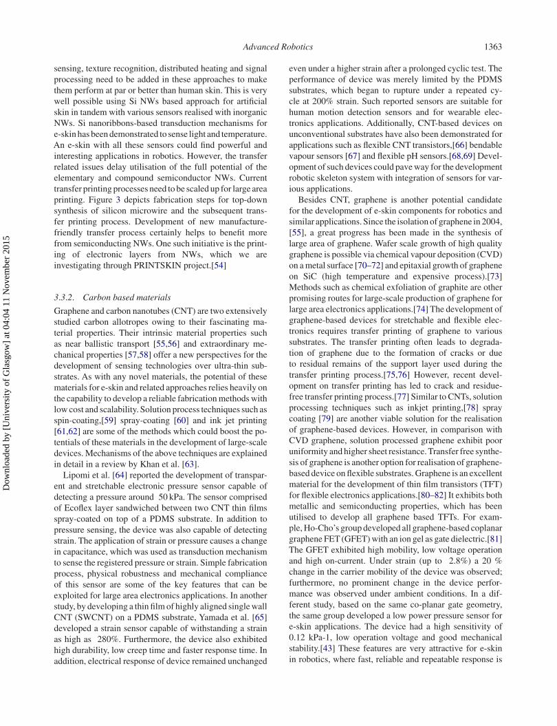
3.3.2. Carbon based materials
Graphene and carbon nanotubes (CNT) are two extensivelystudied carbon allotropes owing to their fascinating ma-terial properties. Their intrinsic material properties suchas near ballistic transport [55,56] and extraordinary me-chanical properties [57,58] offer a new perspectives for thedevelopment of sensing technologies over ultra-thin sub-strates. As with any novel materials, the potential of thesematerials for e-skin and related approaches relies heavily onthe capability to develop a reliable fabrication methods withlow cost and scalability. Solution process techniques such asspin-coating,[59] spray-coating [60] and ink jet printing[61,62] are some of the methods which could boost the po-tentials of these materials in the development of large-scaledevices. Mechanisms of the above techniques are explainedin detail in a review by Khan et al. [63].
Lipomi et al. [64] reported the development of transpar-ent and stretchable electronic pressure sensor capable ofdetecting a pressure around 50 kPa. The sensor comprisedof Ecoflex layer sandwiched between two CNT thin filmsspray-coated on top of a PDMS substrate. In addition topressure sensing, the device was also capable of detectingstrain. The application of strain or pressure causes a changein capacitance, which was used as transduction mechanismto sense the registered pressure or strain. Simple fabricationprocess, physical robustness and mechanical complianceof this sensor are some of the key features that can beexploited for large area electronics applications. In anotherstudy, by developing a thin film of highly aligned single wallCNT (SWCNT) on a PDMS substrate, Yamada et al. [65]developed a strain sensor capable of withstanding a strainas high as 280%. Furthermore, the device also exhibitedhigh durability, low creep time and faster response time. Inaddition, electrical response of device remained unchanged
even under a higher strain after a prolonged cyclic test. Theperformance of device was merely limited by the PDMSsubstrates, which began to rupture under a repeated cy-cle at 200% strain. Such reported sensors are suitable forhuman motion detection sensors and for wearable elec-tronics applications. Additionally, CNT-based devices onunconventional substrates have also been demonstrated forapplications such as flexible CNT transistors,[66] bendablevapour sensors [67] and flexible pH sensors.[68,69] Devel-opment of such devices could pave way for the developmentrobotic skeleton system with integration of sensors for var-ious applications.
Besides CNT, graphene is another potential candidatefor the development of e-skin components for robotics andsimilar applications. Since the isolation of graphene in 2004,[55], a great progress has been made in the synthesis oflarge area of graphene. Wafer scale growth of high qualitygraphene is possible via chemical vapour deposition (CVD)on a metal surface [70–72] and epitaxial growth of grapheneon SiC (high temperature and expensive process).[73]Methods such as chemical exfoliation of graphite are otherpromising routes for large-scale production of graphene forlarge area electronics applications.[74] The development ofgraphene-based devices for stretchable and flexible elec-tronics requires transfer printing of graphene to varioussubstrates. The transfer printing often leads to degrada-tion of graphene due to the formation of cracks or dueto residual remains of the support layer used during thetransfer printing process.[75,76] However, recent devel-opment on transfer printing has led to crack and residue-free transfer printing process.[77] Similar to CNTs, solutionprocessing techniques such as inkjet printing,[78] spraycoating [79] are another viable solution for the realisationof graphene-based devices. However, in comparison withCVD graphene, solution processed graphene exhibit pooruniformity and higher sheet resistance. Transfer free synthe-sis of graphene is another option for realisation of graphene-based device on flexible substrates. Graphene is an excellentmaterial for the development of thin film transistors (TFT)for flexible electronics applications.[80–82] It exhibits bothmetallic and semiconducting properties, which has beenutilised to develop all graphene based TFTs. For exam-ple, Ho-Cho’s group developed all graphene-based coplanargraphene FET (GFET) with an ion gel as gate dielectric.[81]The GFET exhibited high mobility, low voltage operationand high on-current. Under strain (up to 2.8%) a 20 %change in the carrier mobility of the device was observed;furthermore, no prominent change in the device perfor-mance was observed under ambient conditions. In a dif-ferent study, based on the same co-planar gate geometry,the same group developed a low power pressure sensor fore-skin applications. The device had a high sensitivity of0.12 kPa-1, low operation voltage and good mechanicalstability.[43] These features are very attractive for e-skinin robotics, where fast, reliable and repeatable response is
Dow
nloa
ded
by [
Uni
vers
ity o
f G
lasg
ow]
at 0
4:04
11
Nov
embe
r 20
15

1364 N. Yogeswaran et al.
Figure 2. Large area graphene for flexible device applications. (a,b) Transfer printing of roll-to-roll fabricated 30 inch graphene andthe resistive graphene based touch screen film using flexible polyethylene terephthalate (PET) substrates [87].(c) Schematic illustrationand the operation of the broadband optical modulators based on graphene supercapacitors [121]. Application of bias voltage through theelectrolyte medium dopes the graphene layers and yields a transmittance change with the blocking of interband transitions in graphene.(d) Graphene based flexible electrochromic devices [88].
much desired.[2] Other graphene-based solutions, whichcan also be used in robotic systems, are flexible and trans-parent strain sensors,[83] flexible supercapacitors [84] andgas sensors on bendable and soft substrates.[85,86] In thatsense, current focus of the graphene research is the fabrica-tion of large area graphene electrodes on flexible substratesfor touch sensor and smart window applications. Figure 2(a)and (b) show the transfer printing of roll-to-roll fabricated30 inch graphene and touch sensor panel developed usinggraphene on flexible polyethylene terephthalate (PET) sub-strates [87]. Figure 2(c) shows the schematic illustration andthe operation mechanism of the broadband optical modula-tors based on graphene supercapacitors [121]. Applicationof bias voltage through the electrolyte medium dopes thegraphene layers and shifts the Fermi level. This causesthe blocking of interband transitions in graphene whichmakes the material more transparent. Figure 2(d) shows thegraphene based flexible electrochromic devices [88]. Mul-tilayer graphene changes its colour with the intercalationof ions through the graphene layers. At 5 V device allowsto see the University of Glasgow logo placed beneath it.Device operation is stable under mechanical stress.
Given these developments, the integration of graphenesheets onto flexible, ultra-thin and soft substrates couldfind variety of uses in robotic skin ranging from motionsensing to display applications. For example, the usageof large area graphene sheets as flexible and transparent
electrodes [87] in the robotic skin would yield to advancedsensing of many environmental parameters due to high car-rier mobility and high surface coverage. Alternately, us-age of graphene-based flexible electrochromic devices [88]and/or graphene/nanotube-based smart windows [89] couldprovide skin like display panels over the limbs of a hu-manoid to show the information about the current status ofthe system.
3.3.3. Organic materials
Organic semiconductors fuelled the initial developmentsin the field of stretchable and flexible electronics. Thoughthese materials exhibit a poor mobility in comparison withinorganic semiconductors, the low cost and large area fabri-cation compatibility are some of their advantages.Organic materials have tremendous prospective applica-tions for electronic skin applications. Some of the widelyused conductive polymers include poly (3,4-ethylenedioxythiophene):polystyrene sulfonate (PEDOT:PSS), poly(3-hexylthiophene 2,5-diyl) (P3HT), polypyrrole andpolyaniline (PANI). These conductive polymers can be usedas conductive fillers in the composite.[12] Organic semi-conductors are widely used materials in the developmentof flexible electronics. Some of the organic semiconductorsused in the development of e-skin includes pentacene andrubrene.[34,35]
Dow
nloa
ded
by [
Uni
vers
ity o
f G
lasg
ow]
at 0
4:04
11
Nov
embe
r 20
15

Advanced Robotics 1365
Figure 3. Schematic of fabrication steps of silicon wires by top-down approach and the subsequent transfer printing of the wireto a target substrate using PDMS as supporting layer; (a)–(b)silicon microstructure were obtained by lithographic patterningand deep ion reactive etching of SOI wafer; (d)–(e) siliconmicrowire transferred using a plasma exposed PDMS; (f)–(h)silicon microwires transferred to the target substrate and finallythe PDMS was removed.[45]
3.3.4. Stretchable polymer composite
Polymers are an interesting class of materials for the devel-opment of flexible and stretchable electronics owing to theirexcellent mechanical properties. Nevertheless, the poorelectrical conductivity of these materials limits their use tosubstrate and dielectric applications during the developmentof flexible electronic. Introduction of conductive fillers intothe polymers results in a composite with high electricalconductivity and mechanical stretchability.[90–92] Thoughpolymer composites have long been investigated, its poten-tial application has been limited by high filler concentrationwhich has a negative effect on the mechanical properties ofthe composites.[93] Issues such as high filler concentrationcan be obviated by the introduction of nanomaterials. Unliketraditional conductive fillers, the use of nanomaterials asfillers could enable the composites to acquire the desiredproperty at a lower filler concentration.[94,95] Some ofthe widely used nanofillers are graphite nanopallets, NWs,carbon nanotubes (CNT) and graphene. The high aspectratios of nanofillers such as CNT and graphite flakes are thekey reasons behind the low percolation threshold of thesematerials. Percolation threshold is the minimum volumefraction of the conductive filler required for the transitionof the polymer from its insulation to conduction phase.[12]
The transition of the polymer from its insulating to con-ductive phase occurs when the concentration of the fillersexceed the percolation threshold, resulting in a formationof conductive network within the polymer matrix. A lowerpercolation threshold is preferable to retain the elasticityof polymer. The percolation threshold can be influencedby various factors such as type of polymer matrix, size,shape, aspect ratio and surface condition of fillers.[96] Inaddition to aforementioned parameters, uniform dispersionof fillers within the polymer also plays a crucial role inachieving a lower percolation threshold.[97] Dispersion offillers within the polymer can be achieved by various tech-niques such as sonication,[98] ball milling,[99] mechanicalstirring, sheer mixing [100] and surfactant-assisted process.Carbon black an amorphous form of carbon is an attractivecandidate for the development of conductive fillers havebeen used in the development of flexible tensile stress andpressure sensors.[101] Among the list of other filler materi-als, CNT is another attractive candidate as a nanofiller.[94,95] The high aspect ratio of CNT often leads to a lowerpercolation threshold. The realisation of nanocompositesand devices is greatly influenced by patterning technologies.Among the various patterning techniques of composites,the most common technique is moulding. As depicted inFigure 4(a), a master mould made of SU-8 or other UV cur-able material is fabricated with desired structures patternedby standard photolithography. The prepared nanocompositeis then poured onto the mould and cured. Following curingof composite, the polymer substrate is poured on top ofthe patterned conductive composite on the mould. Finally,the bilayer film consisting of polymer substrate/conductivecomposite is peeled from the mould resulting in a patternedstructure of the composite on the substrate.[102,103] An-other popular patterning technology is the micro-contactprinting which relies on the PDMS mould made by castingor machining and transfers the conductive composites ontopolymer substrate shown in Figure 4(b).[104]
3.4. Smart structural engineering
Traditionally, electronics has been developed via use ofinorganic materials and metals. Development of stretchableelectronics utilising these material is highly favourable dueto their superior electronic performance and mature fabrica-tion technology. However, the use of these materials is lim-ited due to their rigid and brittle nature. Dahiya et al. [105]reported development of piezoelectric oxide semiconductorfield effect transistors (POSFET) for robotic tactile applica-tions. The device demonstrated a sensitivity of 102.4 mV/N.Though the device exhibited a good sensitivity, its use inelectronics skin application is limited due to the rigidnessof the POSFET. Such hurdle in the development of flexibleelectronics through the use of intrinsically brittle materialcan be overcome by the smart structural engineering ofthe materials, to accommodate the strain caused due to
Dow
nloa
ded
by [
Uni
vers
ity o
f G
lasg
ow]
at 0
4:04
11
Nov
embe
r 20
15

1366 N. Yogeswaran et al.
Figure 4. (a) Moulding process for patterning CNTs-PDMS composite.[88] (b) Micro-contact printing for patterning CNT-PDMScomposite.[104]
flexing of the materials. Some of the widely used structuralengineering techniques includes: (1) Thinning down of Siwafer (2) Buckling; (3) Use of stretchable interconnects toconnect rigid islands.[106]
3.4.1. Ultra-thin Silicon chips
The organic semiconductor-based analogue and digitalelectronics is not sufficient to meet many challenges, espe-cially those related to high performance requirements andstabilities. They are severely unstable to design analoguecircuit and sensor blocks such as comparators, amplifiersand ADCs.[107] This is mainly due to low charge carriermobility of organic semiconductors, which results in de-vices that are much slower than their inorganic counter-parts. To overcome these challenges, new forms of highmobility material such as single crystal Si nanowires andultra-thin chips have been investigated. Although verypromising, the Si micro-/nanoscale structures basedapproach is still at infancy. On the other hand, ultra-thinflexible chips are promising as they enable compactelectronics and are bendable.
Si chips are traditionally built on wafers whose thick-nesses are in the range of 100 micrometres. These wafersare intrinsically brittle, thus limiting their use in the devel-opment of flexible electronics. Flexibility can be inducedinto Si wafer if it is thinned below 50 µm, in the range of20–50 µm. In addition at 10 µm range, the Si exhibited atransparent nature, therefore enabling its usage in displaysapplications.[108] These ultra-thin flexible Si chips can betransferred onto a polymeric foil to form system in foil (SiF)devices for electronic skin applications.[109] Thinning of Sichips are generally achieved either by physical or chemicalmethods.
Among the physical methods, back grinding of waferis the most popular method for thinning of wafer usinga grinder wheel. Traditionally, the removal rate for backgrinding ranges from 0.1−100µm/min.[110,111] The backgrinding of the sample causes sub surface damage and crackat the edges. The thinned wafers are transferred using acarrier wafer, following which the thin membrane is even-tually removed.[112] In addition, thin Si-based devices andnanomembranes can also be achieved by chemical etchingof SOI (Si on Insulator) wafer. Chemical etching of Si canbe achieved either via both dry and wet etching process. Thethinned Si is removed from SOI wafers by etching the under-lying oxide. Some of the widely used wet etchants of Si areethylenediamine prrocatechol (EDP), potassium hydroxide(KOH), tetramethylammonium hydroxide (TMAH). Wetetching of samples lead to undercutting,[113] which couldbe evaded by using dry etching process. Common dry etch-ing techniques include: (1) Plasma systems; (2) Ion etching;(3) Reactive ion etching. High cost of SOI wafer is anotherlimiting factor. Various alternates for SOI wafers have beenproposed. Some of the techniques include Dicing BeforeGrinding (DBG),[114] thinning of wafer by a combinationof selective wet etching and back grinding process- Thedevices are fabricated on top of epitaxial grown Si. Otheravailable techniques for thinning of chip includes Chip film,Hyperion and Taiko [108,115,116].
Despite progress and achievement of the ultra-thin Sichips in improving of the bendable electronics, the con-ventional BSIM (Berkeley Short-channel IGFET Model)models fail to predict the behaviour of such devices sincethey are appropriate for rigid and planar structures. Thesemodels need to characterise and capture the effects relatedto uniaxial, biaxial and shear stress, which is important fromcircuit design aspect as well as various bendable electronicsapplications.
Dow
nloa
ded
by [
Uni
vers
ity o
f G
lasg
ow]
at 0
4:04
11
Nov
embe
r 20
15

Advanced Robotics 1367
(h)
Figure 5. Fabrication process flow for engineering 3D buckled structure. (a)–(g) Process steps in the formation and 3D buckledsemiconductor nanoribbons and process of incorporating it within the PDMS. (h) Response of the semiconductor nanoribbon underapplication of force.[118].
Figure 6. Percolation path of gold film on a PDMS substrate (a) SEM micrograph of gold film on a PDMS substrate at different strainfrom 0–20%. The random cracks observed at 0% strain is due to mismatch in thermal expansion coefficient PDMS and gold film occurredduring the cooling process following the deposition of gold film. (b) Schematic of conduction percolation pathway on gold film at 0%strain and 20% strain.[120]
Dow
nloa
ded
by [
Uni
vers
ity o
f G
lasg
ow]
at 0
4:04
11
Nov
embe
r 20
15

1368 N. Yogeswaran et al.
3.4.2. Formation of wavy patterns
Buckling is another technique that enables stretchability ofintrinsically inelastic material. It is achieved by depositinga thin film of thin inelastic material on top of a pre-strainedelastomer. Wavy patterns are formed on relaxation. Uniaxialstrain of elastomer results in a linear waveform while abiaxial strain results in 2D herringbone structure.[117] In astudy by Roger’s group, a pop-up structure consisting of Siand GaAs nanoribbons were fabricated and these structureswere capable of withstanding a stretchability and compress-ibility of 100 and 25%, respectively. [118]. The fabrica-tion process flow of this pop-up structure is depicted byFigure 5. A significant advantage of buckling technique isthat it enables the use of inorganic semiconductor mate-rial. Buckling has been demonstrated in various materi-als ranging from metallic, semiconducting and CNT thinfilms. Lipomi et al. [64], demonstrated a transparent pres-sure and strain sensor based on the buckling mechanisms.The developed sensors withstood a strain of 150% alongwith high conductivity. Other similar approaches to attainbuckling include structures such as serpentine and coiledspring etc. These pop-up structures can also be exploited asstretchable interconnects connecting two rigid sections ofthe circuits.[119]
3.4.3. Formation of micro-crack patterns
Formation of intentional micro-cracks is one approach thatcould be used in the development of stretchable electronics.This is achieved by depositing a thin metal film on top of anelastomeric substrate. Continuous loading and unloadingcauses the formation of cracks on the metallic film, theformation of percolation path by the micro-cracks played acritical role in the conductivity of the film. Graz et al. [120]demonstrated the formation of micro-crack on a thin goldfilm deposited on top of PDMS substrate. The film exhib-ited an excellent robustness under a strain of 20% for over250,000 cycles. Figure 6(a) shows the SEM micrographsof micro-cracks formed in on the gold film at differentstrain while Figure 6(b) shows a schematic of percolationconduction path at different strain.
3.5. Summary
Flexibility and stretchability will be the key criterions offuture electronic skin. As described above, this could beachieved either via smart structural engineering and use ofnovel materials. In addition to mechanical robustness, thechoice of the material is also influenced by the application.For instance, PDMS could be used as both a substrate anddielectric based on applications.
The use of smart structural engineering techniques wouldenable the use of well-established silicon technology to de-velop flexible and stretchable e-skin sensors. Furthermore,sensors developed via these technique would enable better
system integration thus aiding easy integration with circuitsof data collection, signal condition and processing of thereceived data.
Novel materials such as nanowires, CNT and grapheneexhibit excellent mechanical and electrical properties whichare critical parameters for the development of e-skin sen-sors. Nevertheless, the use of these novel materials is limitedby the higher fabrication cost and yet to be optimised trans-fer printing that would suit large-scale production of deviceswith similar characteristics. In addition to passive sensors,developed via various transduction mechanisms, develop-ment of transistors using the novel material are highly de-sirable as it would enable the development of active circuitmatrix for large-scale sensing with low power consump-tion. It will also enable easier readout circuit and individualaccess to devices. Development of FET using the novelmaterial is challenging due to various aspects. Graphene forinstance is a zero bandgap material, therefore GFET oftenexhibit a high off-current leading high power consumptionin its off state.
Organic materials are also desirable for the developmentof flexible components for e-skin due to low cost. Someya’sgroup has pioneered the development of organic FET forpressure sensor applications and have developed pressuresensors suitable for robotic fingertip.[34]
4. Conclusions
The development of flexible and stretchable sensors fore-skin applications has seen an unprecedented growth inrecent years. This has to be attributed to development ofnovel material and engineering which has enabled inno-vative devices. Flexible and stretchable e-skin would havesignificant impact on the tactile sensing capability of hu-manoids, therefore will have a critical component of futurehumanoids.
Despite several reported progress in development of flex-ible pressure and strain sensors for e-skin application, thereare still several significant hurdles that need to be addressedto enable mass production. This includes low-cost fabrica-tion process with higher device yield with similar charac-teristics. Other factors such as lower power consumption,device sensitivity, device stability after repeated operation,response time and operation bandwidth are also criticalfactors. More importantly, device integration with systemis crucial for the true success of e-skin for tactile sens-ing of humanoids. This would require development of anelectronic interface consisting components for digitalisationof signal, signal conditioning, data processing and trans-mission of data. Furthermore, the performance of roboticsystem equipped with e-skin will also heavily be governedby the software algorithms processing and learning methodsto distinguish between different tactile data. In addition totactile sensing, other features like self-healing, chemical andbiological sensing can also benefit e-skin. Recent develop-
Dow
nloa
ded
by [
Uni
vers
ity o
f G
lasg
ow]
at 0
4:04
11
Nov
embe
r 20
15

Advanced Robotics 1369
ments have led to e-skin sensors exceeding sensitivity ofhuman skins in terms of detection of human skin. Althoughthere are many issues yet to be addressed, the progressin the development trend in e-skin suggest that humanoidequipped with flexible and stretchable will be possible innear future.
Disclosure statementNo potential conflict of interest was reported by the authors.
FundingThis work was supported by the European Commission undergrant agreement PITN-GA-2012-317488-CONTEST and Engi-neering and Physical Science Council (EPSRC) Fellowship forGrowth – Printable Tactile Skin (EP/M002527/1).
Notes on contributorsN. Yogeswaran received his BEng (Hons) de-gree in Electronic engineering from Universityof Surrey, UK where he specialised in devices.Following his undergraduate degree, he pur-sued a masters degree in Nanoelectronics andNanotechnology at University of Southampton,UK. Currently, he is enrolled as a PhD studentat University of Glasgow, UK. He is currentlycarrying out his research activities at FBK, Italy
under the supervision of Leandro Lorenzelli and Ravinder Dahiya.His research work is focused on the development of physical andchemical sensors on flexible substrate for E-skin applications.
W. Dang is a PhD student at Universityof Glasgow, UK. and a Marie Curie Fellowat Fondazione Bruno Kessler, Trento, Italy.She received an MSc degree in MicrosystemsEngineering from University of Freiburg,Germany. Her work is focused on the stretch-able interconnects and their integration withsensors/actuators on flexible and conformablesubstrates.
W.T. Navaraj received his BE degree inElectronics and Communication Engineeringfrom Anna University-Thiagarajar College ofEngineering in 2009 and MTech degree inAdvanced Semiconductor Electronics fromAcademy of Scientific and Innovative Research(AcSIR) in 2011. Before joining Universityof Glasgow for his PhD, he was working asa Scientist in Sensors and Nanotechnology
Group at CSIR-Central Electronics Engineering Research Institute(CEERI), Pilani, India’s pioneer research institute in the area ofelectronics. His current research interests include flexible elec-tronics, nano-electronic devices and technology, tactile sensing,sensors-to-devices-to-systems, 3D printing prosthetics/robotics.He has won CSIR-QHS Fellowship, best paper awards ininternational conferences, Department Topper during master?sdegree, Child scientist award from NCSTC-DST, District Topperin Higher Secondary Exams, Anna Award from Govt. of TamilNadu and several prizes in various engineering projects and
robotics events. He is a student member of IEEE-UK, IEEE-EDSSociety, IEEE Sensors Council, IEEE Nanotechnology Council,member of IET-UK, associate member of IE (India), life fellow ofOSI.
D. Shakthivel studied MSc Materials Scienceat Bharathiyar University, Coimbatore India.He received his PhD in 2014 from the IndianInstitute of Science, Bangalore, India, workingon growth of semiconducting nanowires byvapour-liquid-solid mechanism using CVDmethod. His research interests focused ongrowth and characterisation of nanowires fornanolectronic devices. Currently, he is working
as a postdoctoral researcher at the School of Engineering,University of Glasgow, United Kingdom. He is working onsemiconducting nanowires for flexible electronic devices.
S. Khan received his masters degree inElectronic Engineering from Jeju NationalUniversity, South Korea, and BS Engineeringfrom GIK Institute of Engg Sciences andTechnology, Pakistan. His research interestsare in the development of flexible thin filmelectronics on large area plastic substratesemploying printing technologies. He is cur-rently a PhD student with the University of
Trento and his research is based within the MicrosystemsTechnology research unit at FBK (Fondazione Bruno Kessler),Trento, under the supervision of Ravinder Dahiya and LeandroLorenzelli. His research focus is development of printing routesfor flexible electronics manufacturing using transfer printing of Simicro/nanostructures on plastic substrates.
E.O. Polat received his BSc degree in physicsfrom Izmir Institute of Technology, Turkey in2009. He got his PhD degree in physics fromBilkent University, Turkey in 2015. He is apost-doctoral research fellow in the Universityof Glasgow. His PhD research covers thegraphene-based optoelectronics. After the firstdemonstration of ‘Synthesis of Graphene onGold’, he and his colleagues from Bilkent
University showed for the first time a ‘Graphene Based OpticalModulator’ working in visible wavelengths. Then, by extendinghis research on multilayer graphene, he created ‘GrapheneBased Flexible Smart Windows’ that can change colour withthe application of voltage. Recently, he and his colleaguesdemonstrated active flexible surfaces that enable electrical controlof reflection, transmission and absorption of microwaves byusing large-area graphene electrodes. He holds 3 patents andmore than 10 publications in high impact factor journals. He isawarded for the ‘Young Scientist Award’ of European MaterialResearch Society (E-MRS) in 2014, and Silver Leaf Award ofIEEE Prime in 2015. Currently, his main focus is integration ofgraphene on unconventional substrates which enables electronicsand optoelectronic devices with new mechanical functionalities.He is with the ‘Bendable Electronics and Sensing Technologies(BEST) Group’ leaded by Ravinder Dahiya in University ofGlasgow and he is working on the heterogeneous integration of Sito graphene-based ultra-thin and flexible devices.
Dow
nloa
ded
by [
Uni
vers
ity o
f G
lasg
ow]
at 0
4:04
11
Nov
embe
r 20
15

1370 N. Yogeswaran et al.
S. Gupta is a first-year PhD student withinthe Department of Electronics and Nano-Scale Engineering, University of Glasgow,UK. He obtained his bachelor’s degree inElectrical Engineering from Indian Institute ofTechnology Kanpur. Currently, he is workingas a Marie Curie fellow at Fondazione BrunoKessler, Italy on flexible POSFET for touchsensing in electronic skin under framework of
CONTEST project. His areas of interest are flexible electronicsand semiconductor physics.
H. Heidari is a Postdoctoral Researcherin Electronic and Nanoscale EngineeringDivision at University of Glasgow, UK. Hereceived BSEE and MSEE degrees in 2005and 2008, respectively. Heidari subsequentlycompleted his PhD in Microelectronics underthe direction of Franco Maloberti fromthe University of Pavia, Italy, where heworked on Integrated CMOS Magnetic Sensor
Microsystems. In past, he worked at Hamrah-e-Avval (MobileTelecommunication Company of Iran) and Azad University, Iran.Heidari served on the local organising committee for the IEEEPRIME 2015 conference held in Glasgow, Scotland. He is amember of IEEE and a reviewer for several international journalsand conferences. He received honorary mention paper award atthe IEEE ISCAS 2014 and gold leaf award at IEEE PRIME 2014conferences. He was a Visiting Scholar at the State Key Laboratoryof Analog and Mixed-Signal VLSI at the University of Macau,China.
M. Kaboli received his bachelors in Electricaland Electronic Engineering and masters inWireless Systems and Signal Processing fromthe Royal Institute of Technology (KTHUniversity) in Stockholm, Sweden, in 2011. Hejoined Idiap lab/EPFL university as a researchassistant in March 2011. Since April 2013, hehas been with the Tactile Sensing Group withGordon Cheng, Institute for Cognitive Systems,
Technische Universit’at M’unchen in Munich, Germany. Hiscurrent research interests include Tactile Learning and TactileTransfer Learning in Robotic Systems.
L. Lorenzelli received the Laurea degree inElectronic Engineering from the Universityof Genova in 1994 and in 1998 the PhD inElectronics Materials and Technologies fromUniversity of Trento. During the PhD, hisresearch activity concerned simulation anddesign of electrochemical microsensors usingCMOS foundry services. Since 1998, he joinedthe staff of the ITC-irst Microsystems Division
and he was involved in the realisation of microsystems forbiomedical, environmental and agro-food applications. Since2005, he directs the BioMEMS research area at FBK-irst (‘BrunoKessler’ Foundation). His research interests include biosensors,nanobiotechnology, lab-on-chip, medical diagnostic and point-of-care devices.
G. Cheng is the professor and chair ofCognitive Systems, and founding director ofthe Institute for Cognitive Systems, TechnischeUniversität München, Munich, Germany. Hewas the Head of the Department of HumanoidRobotics and Computational Neuroscience,ATR Computational Neuroscience Laborato-ries, Kyoto, Japan, from 2002 to 2008. Hewas the group leader for the JST International
Cooperative Research Project, Computational Brain, from 2004to 2008. He was designated a project leader from 2007 to 2008for the National Institute of Information and CommunicationsTechnology of Japan. He has held visiting professorshipsworldwide in multidisciplinary fields comprising mechatronics inFrance, neuroengineering in Brazil and computer science in theUSA. He held fellowships from the Center of Excellence andthe Science and Technology Agency of Japan. Both of thesefellowships were taken at the Humanoid Interaction Laboratory,Intelligent Systems Division at the Electrotechnical Laboratory,Japan. He received the PhD degree in systems engineeringfrom the Department of Systems Engineering, The AustralianNational University, in 2001, and the bachelor?s and master?sdegrees in computer science from the University of Wollongong,Wollongong, Australia, in 1991 and 1993, respectively. Hewas the managing director of the company G.T.I. Computingin Australia. His current research interests include humanoidrobotics, cognitive systems, brain machine interfaces, biomimeticof human vision, human-robot interaction, active vision andmobile robot navigation. He is the co-inventor of approximately15 patents and has co-authored approximately 180 to 250 technicalpublications, proceedings, editorials and book chapters.
R. Dahiya is currently a reader and anEPSRC fellow in Electronics and NanoscaleEngineering with the University of Glasgow,Glasgow, UK. He received the PhD degree fromthe Italian Institute of Technology, Genoa, Italy,and the University of Genoa, Genoa, the MTechdegree from the Indian Institute of TechnologyDelhi, New Delhi, India, and the BTech(Hons.) degree from Kurukshetra University,
Kurukshetra, India. He was with the Netaji Subhas Instituteof Technology, New Delhi, the Italian Institute of Technology,Fondazione Bruno Kessler, Trento, Italy, and the Universityof Cambridge, Cambridge, UK. His research interests includeflexible and printable electronics, tactile sensing, electronic skinand robotics. He has authored over 90 papers, one book, andholds one patent. He received the Marie Curie Fellowship andthe EPSRC Fellowship. He has worked on many internationalprojects and is currently coordinating a European Commission-Funded Initial Training Network on Electronic Skin. Dahiya ison the Editorial Boards of the IEEE SENSORS JOURNAL andthe IEEE TRANSACTIONS ON ROBOTICS. He was the GuestEditor of four Special Journal Issues. He was a recipient of theUniversity Gold Medal in 1999, and two Best Paper Awards at theIEEE conferences.
References[1] Dahiya R, NavarajWT, Khan S, et al. Developing electronic
skin with the sense of touch. Inf. Display. 2015:2–6.[2] Dahiya RS, Mittendorfer P, Valle M, et al. Directions
toward effective utilization of tactile skin: a review. IEEESens. J. 2013;13:4121–4138.
Dow
nloa
ded
by [
Uni
vers
ity o
f G
lasg
ow]
at 0
4:04
11
Nov
embe
r 20
15

Advanced Robotics 1371
[3] Jonathan E, Jack C, Chang L. Development of polyimideflexible tactile sensor skin. J. Micromech. Microeng.2003;13:359–366.
[4] Hasegawa Y, Shikida M, Shimizu T, et al.Amicromachinedactive tactile sensor for hardness detection. Sens. ActuatorsA: Phys. 2004;114:141–146.
[5] Lee MH, Nicholls HR. Review article tactile sensingfor mechatronics’a state of the art survey. Mechatronics.1999;9:1–31.
[6] Tee BCK, Wang C, Allen R, et al. An electrically andmechanically self-healing composite with pressure- andflexion-sensitive properties for electronic skin applications.Nat. Nanotechnol. 2012;7:825–832.
[7] Rogers JA, Someya T, Huang Y. Materials and mechanicsfor stretchable electronics. Science. 2010;327:1603–1607.
[8] Schwartz G, Tee BCK, Mei J, et al. Flexible polymertransistors with high pressure sensitivity for applicationin electronic skin and health monitoring. Nat. Commun.2013;4:1859.
[9] Gong S, Schwalb W, Wang Y, et al. A wearable and highlysensitive pressure sensor with ultrathin gold nanowires.Nat. Commun. 2014;5:3132.
[10] Ma Z. An electronic second skin. Science. 2011;333:830–831.
[11] Dahiya RS, Metta G, Valle M, et al. Tactile sensing-fromhumans to humanoids. IEEE Trans. Rob. 2010;26:1–20.
[12] Dahiya R, Valle M. Tactile sensing technologies. In:Robotic tactile sensing. Netherlands: Springer; 2013. p. 79–136.
[13] Kaboli M, Long A, Cheng G. Humanoids learn touchmodalities identification via multi-modal robotic skin androbust tactile descriptors. Adv. Rob. Forthcoming 2015.
[14] Thomaz AL, Hoffman G, Breazeal C. Reinforcementlearning with human teachers: understanding howpeople want to teach robots. In: The 15th IEEEInternational Symposium on Robot and Human InteractiveCommunication, ROMAN. Hatfield; 2006. p. 352–357.
[15] Argall BD, Billard AG. A survey of tactile human robotinteractions. Rob. Auton. Syst. 2010;58:1159–1176.
[16] Schmitz A, Maiolino P, Maggiali M, et al. Methods andtechnologies for the implementation of large-scale robottactile sensors. IEEE Trans. Rob. 2011;27:389–400.
[17] Mittendorfer P, Cheng G. Humanoid multimodal tactile-sensing modules. IEEE Trans. Rob. 2011;27:401–410.
[18] Kim K, Lee KR, Lee DS, et al. A silicon-based flexibletactile sensor for ubiquitous robot companion applications.J. Phys.: Conf. Ser. 2006;34:399–403.
[19] Mukai T, Hirano S, Kato Y. Fast and accurate tactilesensor system for a human-interactive robot. INTECHOpen Access Publisher; 2008.
[20] Liu H, Greco J, Song X, et al. Tactile image basedcontact shape recognition using neural network. In: IEEEConference on Multisensor Fusion and Integration forIntelligent Systems (MFI). Hamburg; 2012. p. 138–143.
[21] Liu H, Song X, Nanayakkara T, et al. A computationallyfast algorithm for local contact shape and pose classificationusing a tactile array sensor. In: IEEE InternationalConference on Robotics and Automation (ICRA). SaintPaul, MN; 2012. p. 1410–1415.
[22] Jia Y, Tian J. Surface patch reconstruction from ‘One-Dimensional’ tactile data. IEEE Trans. Autom. Sci. Eng.2010;7:400–407.
[23] Song A, Han Y, Hu H, et al. A Novel Texture Sensor forFabric Texture Measurement and Classification. Instrum.Meas. 2014;63:1739–1747.
[24] Oddo CM, Controzzi M, Beccai L, et al. Roughnessencoding for discrimination of surfaces in artificial active-touch. IEEE Trans. Rob. 2011;27:522–533.
[25] Jamali N, Sammut C. Majority voting: material classifica-tion by tactile sensing using surface texture. IEEE Trans.Rob. 2011;27:508–521.
[26] Gates BD, Xu Q, Stewart M, et al. New approaches tonanofabrication: molding, printing, and other techniques.Chem. Rev. 2005;105:1171–1196.
[27] Mi Y, Chan Y, Trau D, et al. Micromolding of PDMSscaffolds and microwells for tissue culture and cellpatterning: a new method of microfabrication by the self-assembled micropatterns of diblock copolymer micelles.Polymer. 2006;47:5124–5130.
[28] Dahiya R, Gottardi G, Laidani N. PDMS residues-free mi-cro/macrostructures on flexible substrates. Microelectron.Eng. 2015;136:57–62.
[29] Lee J, Wu J, Ryu JH, et al. Stretchable semiconductortechnologies with high areal coverages and strain-limitingbehavior: demonstration in high-efficiency dual-junctionGaInP/GaAs photovoltaics. Small. 2012;8:1851–1856.
[30] Irimia-Vladu M, Troshin PA, Reisinger M, et al. Environ-mentally sustainable organic field effect transistors. Org.Electron. 2010;11:1974–1990.
[31] Lee P, Lee J, Lee H, et al. Highly stretchable and highlyconductive metal electrode by very long metal nanowirepercolation network. Adv. Mater. 2012;24:3326–3332.
[32] Wang C, Hwang D, Yu Z, et al. User-interactive electronicskin for instantaneous pressure visualization. Nat. Mater.2013;12:899–904.
[33] Takei K, Takahashi T, Ho JC, et al. Nanowire active-matrixcircuitry for low-voltage macroscale artificial skin. Nat.Mater. 2010;9:821–826.
[34] Someya T, Sekitani T, Iba S, et al. A large-area, flexiblepressure sensor matrix with organic field-effect transistorsfor artificial skin applications. Proc. Nat. Acad. Sci. U.S.A.2004;101:9966—9970.
[35] Mannsfeld SCB, Tee BCK, Stoltenberg RM, et al. Highlysensitive flexible pressure sensors with microstructuredrubber dielectric layers. Nat. Mater. 2010;9:859–864.
[36] Trung TQ, Tien NT, Seol YG, et al. Transparent and flexibleorganic field-effect transistor for multi-modal sensing. Org.Electron. 2012;13:533–540.
[37] Khan S, Dang W, Lorenzelli L, et al. Flexible pressuresensors based on screen printed P(VDF-TrFE) andP(VDF-TrFE)/MWCNTs. IEEE Trans. Semicond. Manuf.Forthcoming 2015.
[38] Lee J, Panzer MJ, He Y, et al. Ion gel gated polymer thin-film transistors. J. Am. Chem. Soc. 2007;129:4532–4533.
[39] Maliakal A, Katz H, Cotts PM, et al. Inorganic oxide core,polymer shell nanocomposite as a high K gate dielectricfor flexible electronics applications. J. Am. Chem. Soc.2005;127:14655—14662.
[40] Schroeder R, Majewski LA, Grell M. High-performanceorganic transistors using solution-processed nanoparticle-filled high-k polymer gate insulators. Adv. Mater.2005;17:1535–1539.
[41] Liu J, Buchholz DB, Hennek JW, et al. All-amorphous-oxide transparent, flexible thin-film transistors. Effi-cacy of bilayer gate dielectrics. J. Am. Chem. Soc.2010;132:11934–11942.
[42] Cho JH, Lee J, Xia Y, et al. Printable ion-gel gate dielectricsfor low-voltage polymer thin-film transistors on plastic.Nat. Mater. 2008;7:900–906.
Dow
nloa
ded
by [
Uni
vers
ity o
f G
lasg
ow]
at 0
4:04
11
Nov
embe
r 20
15

1372 N. Yogeswaran et al.
[43] Sun Q, Kim DH, Park SS, et al. Transparent, low-powerpressure sensor matrix based on coplanar-gate graphenetransistors. Adv. Mater. 2014;26:4735–4740.
[44] Sun Y, Rogers JA. Inorganic semiconductors for flexibleelectronics. Adv. Mater.-Deerfield Beach Weinheim.2007;19:1897–1916.
[45] Dahiya RS, Adami A, Collini C, et al. Fabrication of singlecrystal silicon micro-/nanostructures and transferring themto flexible substrates. Microelectron. Eng. 2012;98:502–507.
[46] Liu X, Long Y-Z, Liao L, et al. Large-scale integrationof semiconductor nanowires for high-performance flexibleelectronics. ACS Nano. 2012;6:1888–1900.
[47] Bryllert T, Wernersson L-E, Löwgren T, et al. Ver-tical wrap-gated nanowire transistors. Nanotechnology.2006;17:S227–S230.
[48] Takahashi T, Takei K, Adabi E, et al. Parallel array in asnanowire transistors for mechanically bendable, ultrahighfrequency electronics. ACS Nano. 2010;4:5855—5860.
[49] Friedman RS, McAlpine MC, Ricketts DS, et al.Nanotechnology High-speed integrated nanowire circuits.Nature. 2005;434:1085–1085.
[50] McAlpine MC, Friedman RS, Jin S, et al. High-performance nanowire electronics and photonics on glassand plastic substrates. Nano Lett. 2003;3:1531–1535.
[51] Dahiya RS, Adami A, Collini C, et al. POSFETtactilesensing chips using CMOS technology. In 2013 IEEESensors; Baltimore, MD; 2013. p. 1–4.
[52] Dahiya RS, Metta G, Valle M, et al. Piezoelectric oxidesemiconductor field effect transistor touch sensing devices.Appl. Phys. Lett. 2009;95:034105.
[53] Wu W, Wen X, Wang ZL. Taxel-addressable matrix ofvertical-nanowire piezotronic transistors for active andadaptive tactile imaging. Science. 2013;340:952–957.
[54] Bendable Electronics & Sensing Technologies Group.[10 August 2015]. Available from: http://www.gla.ac.uk/schools/engineering/research/divisions/ene/researchthemes/micronanotechnology/best/projects/.
[55] Novoselov KS, Geim AK, Morozov SV, et al. Electricfield effect in atomically thin carbon films. Science.2004;306:666–669.
[56] Dürkop T, Getty SA, Cobas E, et al. Extraordinarymobility in semiconducting carbon nanotubes. Nano Lett.2004;4:35–39.
[57] Frank IW, Tanenbaum DM, van der Zande AM, et al.Mechanical properties of suspended graphene sheets. J.Vac. Sci. Technol. B. 2007;25:2558–2561.
[58] Krishnan A, Dujardin E, Ebbesen TW, et al. Young’smodulus of single-walled nanotubes. Phys. Rev. B.1998;58:14013–14019.
[59] Jo JW, Jung JW, Lee JU, et al. Fabrication of highlyconductive and transparent thin films from single-walledcarbon nanotubes using a new non-ionic surfactant via spincoating. ACS Nano. 2010;4:5382–5388.
[60] Schindler A, Brill J, Fruehauf N, et al. Solution-depositedcarbon nanotube layers for flexible display applications.Phys. E: Low-dimension. Syst. Nanostruct. 2007;37:119–123.
[61] Kordás K, Mustonen T, Tóth G, et al. Inkjet printingof electrically conductive patterns of carbon nanotubes.Small. 2006;2:1021–1025.
[62] Okimoto H, Takenobu T, Yanagi K, et al. Tunable carbonnanotube thin-film transistors produced exclusively viainkjet printing. Adv. Mater. 2010;22:3981–3986.
[63] Khan S, Lorenzelli L, Dahiya RS. Technologies for printingsensors and electronics over large flexible substrates: areview. IEEE Sens. J. 2015;15:3164–3185.
[64] Lipomi DJ, Vosgueritchian M, Tee BCK, et al. Skin-likepressure and strain sensors based on transparent elasticfilms of carbon nanotubes. Nat. Nanotechnol. 2011;6:788–792.
[65] Yamada T, Hayamizu Y, Yamamoto Y, et al. A stretchablecarbon nanotube strain sensor for human-motion detection.Nat. Nanotechnol. 2011;6:296–301.
[66] Artukovic E, Kaempgen M, Hecht DS, et al. Transparentand flexible carbon nanotube transistors. Nano Lett.2005;5:757–760.
[67] Parikh K, Cattanach K, Rao R, et al. Flexible vapour sensorsusing single walled carbon nanotubes. Sens. Actuators B:Chem. 2006;113:55–63.
[68] Kaempgen M, Roth S. Transparent and flexible carbonnanotube/polyaniline pH sensors. J. Electroanal. Chem.2006;586:72–76.
[69] Ferrer-Anglada N, Kaempgen M, Roth S. Transparentand flexible carbon nanotube/polypyrrole and carbonnanotube/polyaniline pH sensors. Phys. Status Solidi (B).2006;243:3519–3523.
[70] Li X, Cai W, An J. Large-area synthesis of high-qualityand uniform graphene films on copper foils. Science.2009;324:1312–1314.
[71] Bae S, Kim H, Lee Y, et al. Roll-to-roll production of30-inch graphene films for transparent electrodes. NatNanotechnol. 2010;5:574–578.
[72] Polat EO, Balci O, Kakenov N, et al. Synthesis ofgraphene on ultra-smooth copper foils for large area flexibleelectronics. In: 11th International Conference on PhDResearch in Microelectronics & Electronics (IEEE Prime2015); Glasgow; 2015. p. 53–56.
[73] Emtsev KV, Bostwick A, Horn K, et al. Towards wafer-sizegraphene layers by atmospheric pressure graphitization ofsilicon carbide. Nat. Mater. 2009;8:203–207.
[74] Segal M. Selling graphene by the ton. Nat. Nanotechnol.2009;4:612–614.
[75] Li X, Zhu Y, Cai W, et al. Transfer of large-area graphene films for high-performance transparentconductive electrodes. Nano Lett. 2009;9:4359–4363.
[76] Kim KS, Zhao Y, Jang H, et al. Large-scale pattern growthof graphene films for stretchable transparent electrodes.Nature. 2009;457:706–710.
[77] Liang X, Sperling BA, Calizo I, et al. Toward clean andcrackless transfer of graphene. ACS Nano. 2011;5:9144–9153.
[78] Dua V, Surwade SP, Ammu S, et al. All-organic vaporsensor using inkjet-printed reduced graphene oxide.Angew. Chem. Int. Ed. 2010;49:2154–2157.
[79] Pham VH, Cuong TV, Hur SH, et al. Fast and simplefabrication of a large transparent chemically-convertedgraphene film by spray-coating. Carbon. 2010;48:1945–1951.
[80] Kim BJ, Jang H, Lee S-K, et al. High-performanceflexible graphene field effect transistors with ion gel gatedielectrics. Nano Lett. 2010;10:3464–3466.
[81] Kim BJ, Lee S-K, Kang MS, et al. Coplanar-gatetransparent graphene transistors and inverters on plastic.ACS Nano. 2012;6:8646–8651.
[82] Lee S-K, Kim BJ, Jang H, et al. Stretchable graphenetransistors with printed dielectrics and gate electrodes.Nano Lett. 2011;11:4642–4646.
Dow
nloa
ded
by [
Uni
vers
ity o
f G
lasg
ow]
at 0
4:04
11
Nov
embe
r 20
15

Advanced Robotics 1373
[83] Bae SH, Lee Y, Sharma BK, et al. Graphene-basedtransparent strain sensor. Carbon. 2013;51:236–242.
[84] Wu Q, Xu YX, Yao ZY, et al. Supercapacitors based onflexible graphene/polyaniline nanofiber composite films.ACS Nano. 2010;4:1963–1970.
[85] Yi J, Lee JM, Il Park W. Vertically aligned ZnOnanorods and graphene hybrid architectures for high-sensitive flexible gas sensors. Sens. Actuators B-Chem.2011;155:264–269.
[86] Jeong HY, Lee DS, Choi HK, et al. Flexible room-temperature NO2 gas sensors based on carbon nan-otubes/reduced graphene hybrid films. Appl. Phys. Lett.2010;96.
[87] Bae S, Kim H, Lee Y, et al. Roll-to-roll production of30-inch graphene films for transparent electrodes. Nat.Nanotechnol. 2010;5:574–578.
[88] Polat EO, Balci O, Kocabas C. Graphene based flexibleelectrochromic devices. Sci. Rep. 2014;4:6484.
[89] Bonaccorso F, Sun Z, Hasan T, et al. Graphene photonicsand optoelectronics. Nat. Photonics. 2010;4:611–622.
[90] Lu N, Lu C, Yang S, et al. Highly sensitive skin-mountablestrain Gauges based entirely on elastomers. Adv. Funct.Mater. 2012;22:4044–4050.
[91] Cai L, Song L, Luan P, et al. Super-stretchable, transparentcarbon nanotube-based capacitive strain sensors for humanmotion detection. Sci. Rep. 2013;3:3048.
[92] Ding H, Feng T, Chen Y, et al. Field emission propertiesof carbon nanotubes in a stretchable polydimethylsiloxanematrix. Appl. Surf. Sci. 2012;258:5191–5194.
[93] Niu X, Peng S, Liu L, et al. Characterizing and patterningof PDMS-based conducting composites. Adv. Mater.-Deerfield Beach Weinheim. 2007;19:2682–2686.
[94] Khosla A, Gray BL. Preparation, characterizationand micromolding of multi-walled carbon nanotubepolydimethylsiloxane conducting nanocomposite polymer.Mater. Lett. 2009;63:1203–1206.
[95] Lee J-B, Khang D-Y. Electrical and mechanicalcharacterization of stretchable multi-walled carbonnanotubes/polydimethylsiloxane elastomeric compositeconductors. Compos. Sci. Technol. 2012;72:1257–1263.
[96] Li L, Chung DDL. Electrically conducting powder filledpolyimidesiloxane. Composites. 1991;22:211–218.
[97] HuangYY, Terentjev EM. Tailoring the electrical propertiesof carbon nanotube polymer composites. Adv. Funct.Mater. 2010;20:4062–4068.
[98] Ajayan PM, Stephan O, Colliex C, et al. Aligned carbonnanotube arrays formed by cutting a polymer resinnanotube composite. Science. 1994;265:1212–1214.
[99] Yoshio S, Tatami J,Yamakawa T, et al. Dispersion of carbonnanotubes in ethanol by a bead milling process. Carbon.2011;49:4131–4137.
[100] Gojny FH, Wichmann MHG, Köpke U, et al. Carbonnanotube-reinforced epoxy-composites: enhanced stiffnessand fracture toughness at low nanotube content. Compos.Sci. Technol. 2004;64:2363–2371.
[101] Knite M, Teteris V, Kiploka A, et al. Polyisoprene-carbonblack nanocomposites as tensile strain and pressure sensormaterials. Sens. Actuators A: Phys. 2004;110:142–149.
[102] Khosla A, Gray BL. Preparation, micro-patterningand electrical characterization of functionalized carbon-nanotube polydimethylsiloxane nanocomposite polymer.Macromol. Symp. 2010;297:210–218.
[103] Mohamed I, Kay G. Fabrication of micro pillars usingmultiwall carbon nanotubes/polymer nanocomposites. J.Micromech. Microeng. 2013;23:055012.
[104] Chao-Xuan L, Jin-Woo C. Patterning conductive PDMSnanocomposite in an elastomer using microcontactprinting. J. Micromech. Microeng. 2009;19:085019.
[105] Dahiya RS, Adami A, Pinna L, et al. Tactile sensing chipswith POSFET array and integrated interface electronics.IEEE Sens. J. 2014;14:3448–3457.
[106] Lacour SP, Jones J, Wagner S, et al. Stretchableinterconnects for elastic electronic surfaces. Proc. IEEE.2005;93:1459–1467.
[107] Heidari H, Wacker N, Roy S, et al. Towards bendableCMOS magnetic sensors. In: 11th Conference on Ph.D.Research in Microelectronics and Electronics (PRIME);July 2015. Glasgow; 2015. p. 314–317.
[108] Burghartz JN, Harendt C, Tu H, et al. Ultra-thin chipfabrication for next-generation silicon processes. In:Bipolar, BiCMOS Circuits and Technology Meeting,BCTM 2009; IEEE; Capri; 2009. p. 131–137.
[109] Dahiya RS, Gennaro S. Bendable ultra-thin chips onflexible foils. IEEE Sens. J. 2013;13:4030–4037.
[110] Landesberger C, Paschke C, Spöhrle H-P, Bock K.Handbook of 3D integration. Vol. 3. Wiley; Weinheim,Germany; 2014.
[111] Tian YB, Kang RK, Guo DM, et al. Investigation onmaterial removal rate in rotation grinding for large-scalesilicon wafer. Mater. Sci. Forum. 2004;471:7. p. 362–368.
[112] Pei ZJ, Fisher GR, Liu J. Grinding of silicon wafers: areview from historical perspectives. Int. J. Mach. ToolsManuf. 2008;48:1297–1307.
[113] Biswas K, Kal S. Etch characteristics of KOH, TMAH anddual doped TMAH for bulk micromachining of silicon.Microelectron. J. 2006;37:519–525.
[114] Landesberger C, Klink G, Schwinn G, et al. New dicing andthinning concept improves mechanical reliability of ultrathin silicon. In: Proceedings. International Symposium onAdvanced Packaging Materials: Processes, Properties andInterfaces; Braselton, GA; 2001. p. 92–97.
[115] Dekker R, Dumling M, Fock JH, et al. A 10 µm thick RF-ID tag for chip-in-paper applications. In: Proceedings of theBipolar/BiCMOS Circuits and Technology Meeting. SantaBarbara, CA; 2005. p. 18–21.
[116] Smick T, Ryding G, Glavish H, et al. Ion implant apparatusand a method of implanting ions. Google Patents; USpatent; 2014.
[117] Choi WM, Song J, Khang D-Y, et al. Biaxially stretchable“Wavy” silicon nanomembranes. Nano Lett. 2007;7:1655–1663.
[118] Sun Y, Choi WM, Jiang H, et al. Controlled bucklingof semiconductor nanoribbons for stretchable electronics.Nat. Nanotechnol. 2006;1:201–207.
[119] Ko HC, Stoykovich MP, Song J, et al. A hemisphericalelectronic eye camera based on compressible siliconoptoelectronics. Nature. 2008;454:748–753.
[120] Graz IM, Cotton DPJ, Lacour SP. Extended cyclic uniaxialloading of stretchable gold thin-films on elastomericsubstrates. Appl. Phys. Lett. 2009;94:071902.
[121] Polat EO, Kocabas C. Broadband Optical ModulatorsBased on Graphene Supercapacitors. Nano Letters.13:5851–5857.
Dow
nloa
ded
by [
Uni
vers
ity o
f G
lasg
ow]
at 0
4:04
11
Nov
embe
r 20
15