Neurmorphic Architectures Kenneth Rice and Tarek Taha Clemson University.
17
Neurmorphic Architectures Kenneth Rice and Tarek Taha Clemson University
-
Upload
logan-bates -
Category
Documents
-
view
213 -
download
0
Transcript of Neurmorphic Architectures Kenneth Rice and Tarek Taha Clemson University.

Neurmorphic Architectures
Kenneth Rice and Tarek TahaClemson University

Historical Highlights

Analog VLSICarver Mead and his
students pioneered the development aVLSI technology for use in neural circuits
They developed a silicon retina which electronically emulated the first 3 layers of the retina Image from [3]

Artificial Neural Network ChipsEarly neuromorphic architectures were
artificial neural network chipsExamples:
ETANN : (1989) Entirely analog chip that was designed for feed forward artificial neural network operation.
Ni1000 : (1996) Significantly more powerful than ETANN, however has narrower functionality
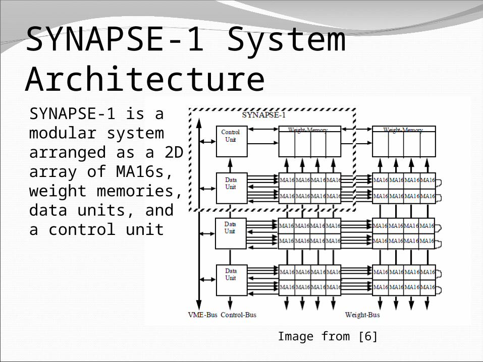
SYNAPSE-1 System Architecture
Image from [6]
SYNAPSE-1 is a modular system arranged as a 2D array of MA16s, weight memories, data units, and a control unit

Modern Architectures:Custom Circuits

Neurogrid(2005) Neurogrid is a multi-chip system
developed by Kwabena Boahen and his group at Stanford University [9]Objective is to emulate neurons Composed of a 4x4 array of NeurocoresEach Neurocore contains a 256x256 array of
neuron circuits with up to 6,000 synapse connections

The FACETS Project(2005) Fast Analog
Computing with Emergent Transient States (FACETS)A project designed by
an international collective of scientists and engineers funded by the European Union
Recently developed a chip containing 200,000 neuron circuits connected by 50 million synapses.
Image from [9]

Torres-Huitzil: FPGA ModelTorres-Huitzil et. al (2005) designed an
hardware architecture for a bio-inspired neural model for motion estimation. Architecture has 3 basic components which
perform spatial, temporal, and excitatory-inhibitory connectionist processing.
Observed approximately 100 x speedup over Pentium 4 processor implementation for 128x128 images

CMOL based designDeveloped by Dan Hammerstrom

HTM on FPGAsImplemented on a Cray XD1
Level 2
AMD Processor
Level 1
AMD Processor
FPGA PEPE FPGA PEPE
AMD Processor
Off-ChipMemory
Off-ChipMemory
Level 2
AMD Processor
Level 1
Level 3
AMD Processor
FPGA PEPE FPGA PEPE
AMD Processor
Off-ChipMemory
Off-ChipMemory
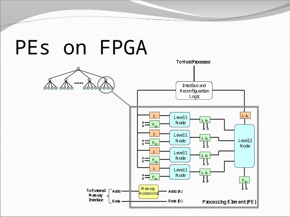
PEs on FPGATo Host Processor
Interface and Reconfiguration
Logic
Level 2Node
Pxu
λ /π
Addr Addr (A)Memory
Access UnitA D
Data (D)Data
To External Memory Interface Processing Element (PE)
λ /πPxu
λ
A D
AD
λ
Pxu
λ /πLevel 1Node
A D
AD
A DPxu
λλ /π
Level 1NodeA
D
Pxu
λλ /π
Level 1Node
A D
AD
Level 1Node
To Host Processor
Interface and Reconfiguration
Logic
Level 2Node
Pxu
λ /π
Addr Addr (A)Memory
Access UnitA D
Data (D)Data
To External Memory Interface Processing Element (PE)
λ /πPxu
λ
A DA D
ADAD
λ
Pxu
λ /πLevel 1Node
A D
AD
A DPxu
λλ /π
Level 1NodeA
D
Pxu
λλ /π
Level 1Node
A DA D
ADAD
Level 1Node
To Host Processor
Interface and Reconfiguration
Logic
Level 2Node
Pxu
λ /π
Addr Addr (A)Memory
Access UnitA D
Data (D)Data
To External Memory Interface Processing Element (PE)
λ /πPxu
λ
A D
AD
λ
Pxu
λ /πLevel 1Node
A D
AD
A DPxu
λλ /π
Level 1NodeA
D
Pxu
λλ /π
Level 1Node
A D
AD
Level 1Node
To Host Processor
Interface and Reconfiguration
Logic
Level 2Node
Pxu
λ /π
Addr Addr (A)Memory
Access UnitA D
Data (D)Data
To External Memory Interface Processing Element (PE)
λ /πPxu
λ
A DA D
ADAD
λ
Pxu
λ /πLevel 1Node
A D
AD
A DPxu
λλ /π
Level 1NodeA
D
Pxu
λλ /π
Level 1Node
A DA D
ADAD
Level 1Node

Large Scale SimulationsIBM:
Blue Brain Project: IBM & EPFL (Switzerland)
IBM Almaden Research Center
Los Alamos National Lab
Air Force Research Laboratory (Rome, NY)
Academia:
Portland State University
Royal Institute of Technology (KTM, Sweden)

AFRL PS3 Cluster

For more informationVisit Institute of Neuromorphic Engineering:
http://www.ine-web.org/

References[1] Neuromorphic,
<http://en.wikipedia.org/wiki/Neuromorphic>.[2] Hammerstrom, D. “A Survey of Bio-Inspired and Other
Alternative Architectures,” in Waser, Rainer (ed.) Nanotechnology. Volume 4: Information technology II. Weinheim: Wiley-VCH, pp. 251-282, 2006.
[3] Carver Mead, <http://en.wikipedia.org/wiki/Carver_Mead>[4] Holler, M., et al. “An Electrically Trainable Artificial Neural
Network (ETANN) with 10240 "Floating Gate” Synapses,” International Joint Conference on Neural Networks, 1989.
[5] Nestor, I., Ni1000 Recognition Accelerator - Data Sheet, 1-7, 1996.
[6] Ramacher, U. et al. “SYNAPSE-1: a high-speed general purpose parallel neurocomputer system, “ IPPS ( 774-781). 1995.

References[7] R. Serrano-Gotarredona, T. et al. “A Neuromorphic Cortical Layer
Microchip for Spike Based Event Processing Vision Systems,” IEEE Trans. on Circuits and Systems, Part-I. Vol. 53, No. 12, pp. 2548-2566, December 2006.
[8] Serrano-Gotarredona, R., et al. “AER Building Blocks for Multi-Layer Multi-Chip Neuromorphic Vision Systems,” , Advances in Neural Information Processing Systems (NIPS), 18: 1217-1224, Dec, Y. Weiss and B. Schölkopf and J. Platt (Eds.), MIT Press, 2005
[9] Brains in Silicon,<http://www.stanford.edu/group/brainsinsilicon/index.html >.
[10] FACETS: Fast Analog Computing with Emergent Transient States, <http://facets.kip.uni-heidelberg.de/index.html>.
[11] Graham-Rowe, D. “Building a Brain on a Silicon Chip,” in Technology Review, March 25, 2009. [Online]. Available: <http://www.technologyreview.com/computing/22339/page1/ >. [ Accessed March 28, 2009].
[12] C. Torres-Huitzil, et. al. “On-chip Visual Perception of Motion: A Bio-inspired Connectionist Model on FPGA, “ Neural Networks Journal, 18(5-6):557-565, 2005.