NASA HANDBOOK NASA-HDBK 8739 · handbook provides guidance that, if applied, may increase...
161
NASA HANDBOOK NASA-HDBK 8739.23A National Aeronautics and Space Administration Washington, DC 20546 Approved: 02-02-2016 Superseding: NASA-HDBK-8739.23 With Change 1 NASA COMPLEX ELECTRONICS HANDBOOK FOR ASSURANCE PROFESSIONALS MEASUREMENT SYSTEM IDENTIFICATION: METRIC APPROVED FOR PUBLIC RELEASE – DISTRIBUTION IS UNLIMITED
Transcript of NASA HANDBOOK NASA-HDBK 8739 · handbook provides guidance that, if applied, may increase...

NASA HANDBOOK NASA-HDBK 8739.23A
National Aeronautics and Space Administration Washington, DC 20546
Approved: 02-02-2016 Superseding: NASA-HDBK-8739.23
With Change 1
NASA COMPLEX ELECTRONICS HANDBOOK FOR ASSURANCE PROFESSIONALS
MEASUREMENT SYSTEM IDENTIFICATION: METRIC
APPROVED FOR PUBLIC RELEASE – DISTRIBUTION IS UNLIMITED

NASA-HDBK 8739.23A—2016-02-02
2 of 161
Mars Exploration Rover (2003)

NASA-HDBK 8739.23A—2016-02-02
3 of 161
DOCUMENT HISTORY LOG
Status Document Revision
Approval Date Description
Baseline 2011-02-16 Initial Release
(JWL4)
Change 1 2011-03-29 Editorial correction to page 2 figure caption
(JWL4)
Revision A 2016-02-02
Significant changes were made in this revision, including: expanded content;
reflected terminology and technology from the NASA-HDBK-4008, Programmable
Logic Devices (PLD) Handbook (released in 2013); eliminated duplication with the PLD
Handbook; and, incorporated other clarifications and corrections.
(MW)

NASA-HDBK 8739.23A—2016-02-02
4 of 161
This page intentionally left blank.


NASA-HDBK 8739.23A—2016-02-02
6 of 161
This page intentionally left blank.
NASA-HDBK 8739.23A—2016-02-02
7 of 161
TABLE OF CONTENTS
1 OVERVIEW ................................................................................................................ 12
1.1 Purpose .......................................................................................................................... 12
1.2 Scope ............................................................................................................................. 12
1.3 Anticipated Audience .................................................................................................... 13
1.4 Handbook Layout .......................................................................................................... 14
2 REFERENCE DOCUMENTS AND LINKS ............................................................ 15
2.1 Reference Documents ................................................................................................... 15 2.1.1 Government Documents ............................................................................................... 15 2.1.2 International Standards ................................................................................................. 16
2.2 Links ............................................................................................................................. 17
3 DEFINITIONS AND ACRONYMS .......................................................................... 18
3.1 Definitions..................................................................................................................... 18
3.2 Acronyms ...................................................................................................................... 24
4 COMPLEX ELECTRONICS OVERVIEW ............................................................ 26
4.1 Configurable Versus Non-Configurable Devices ......................................................... 26 4.1.1 How does Programmable Logic differ from Firmware? ............................................... 27 4.1.2 Comparing Complex Electronics and Software ............................................................ 27
4.2 Programmable versus Designable Devices ................................................................... 28
4.3 Concerns and Issues ...................................................................................................... 28 4.3.1 Verification Issues with Complex Electronics .............................................................. 28
4.4 Summary ....................................................................................................................... 29
5 QUALITY ASSURANCE ON A PLD....................................................................... 30
5.1 Process Assurance Overview ........................................................................................ 30
5.2 Why Do Process Assurance? ........................................................................................ 30
5.3 Tools of the Process Assurance Trade .......................................................................... 32 5.3.1 Documentation Review ................................................................................................. 32 5.3.2 Formal Inspections, Reviews, and Walkthroughs ......................................................... 32 5.3.3 Audits ............................................................................................................................ 33 5.3.4 Analyses ........................................................................................................................ 33
5.4 Identifying Complex Electronics .................................................................................. 33 5.4.1 Simple versus Complex ................................................................................................ 33 5.4.2 How to Determine if Complex Electronics are being developed by a Project ............. 34

NASA-HDBK 8739.23A—2016-02-02
8 of 161
5.4.3 What Next? ................................................................................................................... 34
6 DESIGN PROCESS .................................................................................................... 36
6.1 Overview of the Complex Electronics Design Process ................................................ 36
6.2 Design Life Cycle ......................................................................................................... 36
6.3 Criticality Assessment .................................................................................................. 41
6.4 Process Assurance Activities ........................................................................................ 42
6.5 Planning and Requirements Phase ................................................................................ 43 6.5.1 Planning ........................................................................................................................ 43 6.5.2 Requirements ................................................................................................................ 48 6.5.3 Assurance Roles ............................................................................................................ 50
6.6 Preliminary Design Phase ............................................................................................. 52 6.6.1 Roles of the Engineering Design Team ........................................................................ 52 6.6.2 Assurance Roles ............................................................................................................ 52
6.7 Detailed Design Phase .................................................................................................. 53 6.7.1 Roles of the Engineering Design Team ........................................................................ 53 6.7.2 Assurance Roles ............................................................................................................ 53
6.8 Design Implementation Phase....................................................................................... 53 6.8.1 Synthesis ....................................................................................................................... 54 6.8.2 Simulation ..................................................................................................................... 54 6.8.3 Test Benches ................................................................................................................. 56 6.8.4 Implement the Design ................................................................................................... 57 6.8.5 Programming the Device .............................................................................................. 59 6.8.6 Assurance Roles During Implementation ..................................................................... 59
6.9 Verification ................................................................................................................... 62 6.9.1 What Should an Assurance Person Look for? .............................................................. 63
7 PLDS DEVELOPED BY A SUPPLIER ................................................................... 64
8 METRICS .................................................................................................................... 65
9 SUPPORTING PROCESSES .................................................................................... 66
9.1 Configuration Management (CM) ................................................................................ 66
9.2 Reliability ...................................................................................................................... 66
9.3 Maintenance and Maintainability ................................................................................. 66
10 FUTURE TRENDS ..................................................................................................... 68
10.1 Changes in Complex Electronics Design and Verification ........................................... 68 10.1.1 Hardware/software Codesign and Coverification ......................................................... 68 10.1.2 System Modeling .......................................................................................................... 69
10.2 Into the Not-So-Distant Future ..................................................................................... 70

NASA-HDBK 8739.23A—2016-02-02
9 of 161
10.2.1 In-field or Reconfigurable SoC ..................................................................................... 70 10.2.2 FPGA Microprocessors/Systems .................................................................................. 71 10.2.3 Reconfigurable Computing ........................................................................................... 71
10.3 NASA Assurance Changes ........................................................................................... 72
APPENDIX A THE HISTORY OF COMPLEX ELECTRONICS ................................ 74
A.1 A Bit of History ............................................................................................................ 74
A.2 Simple Programmable Logic Devices .......................................................................... 74
A.3 Complex Programmable Logic Devices (CPLD) ......................................................... 76
A.4 Field Programmable Gate Array (FPGA) ..................................................................... 78
A.5 Application Specific Integrated Circuit (ASIC) ........................................................... 79
A.6 System-on-Chip (SoC) .................................................................................................. 79
A.7 How Complex Electronis Devices Remember Their Configuration ............................ 80
APPENDIX B HARDWARE DESCRIPTION LANGUAGES ....................................... 84
B.1 Overview of Hardware Description Languages (HDLs) .............................................. 84
B.2 General Hardware Description Language Concepts ..................................................... 84
B.3 Programming ExampleS ............................................................................................... 91
B.4 Abstraction .................................................................................................................... 93
APPENDIX C EXAMPLES ................................................................................................ 96
C.1 CPLD ............................................................................................................................ 96
C.2 FPGA .......................................................................................................................... 101
C.3 ASIC ........................................................................................................................... 107
C.4 SoC .............................................................................................................................. 113
C.5 Reconfigurable Computing ......................................................................................... 120
APPENDIX D CODING STYLE GUIDELINES ............................................................ 126
D.1 Introduction ................................................................................................................. 126
D.2 Top-Down Design ....................................................................................................... 126
D.3 Signals and Variables .................................................................................................. 133
D.4 Packages ...................................................................................................................... 137
D.5 Technology-Specific Code (Xilinx) ............................................................................ 141
D.6 Coding for Synthesis ................................................................................................... 150
APPENDIX E PLD ASSESSMENT FORM .................................................................... 160

NASA-HDBK 8739.23A—2016-02-02
10 of 161
LIST OF TABLES
Table 1: Complexity Guidelines ............................................................................................ 33 Table 2: CE vs. SW Development Phases ............................................................................. 39 Table 3: PLD Artifacts for Each Milestone ........................................................................... 41 Table 4: PLD Assurance Effort .............................................................................................. 42 Table 5: Requirement Verification Activities ........................................................................ 51 Table 6: Design Verification Activities ................................................................................. 52 Table 7: Design Implementation Verification Activities ....................................................... 54 Table 8: Verification Activities.............................................................................................. 62 Table A-1: Simple PLD Comparisons ....................................................................................... 76 Table A-2: FPGA vs. ASIC Comparison ................................................................................... 82 Table B-1: VHDL vs. Verilog.................................................................................................... 88
LIST OF FIGURES
Figure 1: How Complex Electronics Compares ...................................................................... 26 Figure 2: Generic CE Waterfall Development ........................................................................ 37 Figure 3: Quality Assurance Support for PLD Development ................................................. 40 Figure 4: Complex Electronics Design Views ........................................................................ 45 Figure A-1: Example of PAL Structure ....................................................................................... 75 Figure A-2: CPLD vs. FPGA Layout .......................................................................................... 78 Figure A-3: SoC Example Configuration .................................................................................... 79 Figure A-4: External Programmer ............................................................................................... 81 Figure B-1: General HDL Development ..................................................................................... 87 Figure B-2: AOI VHDL to Verilog Comparison ........................................................................ 92 Figure B-3: Complex Electronics Domains ................................................................................ 94 Figure B-4: Warning Buzzer Example ........................................................................................ 94 Figure C-1: CPLD ....................................................................................................................... 96 Figure C-2: MIDN ....................................................................................................................... 99 Figure C-3: FCF ........................................................................................................................ 100 Figure C-4: FGPA ..................................................................................................................... 101 Figure C-5: Other CPLD Missions ............................................................................................ 106 Figure C-6: ASIC ...................................................................................................................... 107 Figure C-7: ASIC Die................................................................................................................ 109 Figure C-11: SOC ........................................................................................................................ 113 Figure C-12: Reconfigurable SoC ............................................................................................... 116 Figure C-13: ChipSat OBC ......................................................................................................... 119 Figure D-1: Behavioral Code .................................................................................................... 126 Figure D-2: Structural Code ...................................................................................................... 127 Figure D-3: One Line Per Signal/Named Association .............................................................. 128 Figure D-4: Header Template .................................................................................................... 129 Figure D-5: Process, Function, and Procedure Header ............................................................. 129

NASA-HDBK 8739.23A—2016-02-02
11 of 161
Figure D-6: Inline Comments .................................................................................................... 130 Figure D-7: Proper Indentation.................................................................................................. 130 Figure D-8: Confusing_in and_out suffixes .............................................................................. 132 Figure D-9: Internal Signals Representing Output Ports ........................................................... 133 Figure D-10: Correct Use of Variables........................................................................................ 136 Figure D-11: Incorrect Use of Variables ..................................................................................... 136 Figure D-12: A Constant Guiding the Generation of Logic ........................................................ 138 Figure D-13: Address Width Defined by a Constant .................................................................. 139 Figure D-14: Modular Function Use ........................................................................................... 140 Figure D-15: Use of Types and Aliases ...................................................................................... 141 Figure D-16: Three-state Implementation of 4:1 Multiplexer ..................................................... 144 Figure D-17: Xilinx LUT-RAM Inference .................................................................................. 145 Figure D-18: LUT-ROM Inference ............................................................................................. 146 Figure D-19: Virtex Block RAM inference ................................................................................. 146 Figure D-20: Clock Enable Inference .......................................................................................... 148 Figure D-21: Inference of Xilinx Shift Register LUT (SRL) ...................................................... 149 Figure D-22: Local Asynchronous Reset and TC & Well-Behaved Synchronous Reset & CE . 152 Figure D-23: Well Behaved Local Asynchronous Reset and TC & Well-Behaved Synchronous
Reset & CE ............................................................................................................ 152 Figure D-24: Priority Encoded Logic .......................................................................................... 157 Figure D-25: For-Loop Cascaded Logic Implementation ........................................................... 158 Figure D-26: Latch Inference ...................................................................................................... 159 Figure D-27: Elimination of Inadvertent Latch Inference ........................................................... 159

NASA-HDBK 8739.23A—2016-02-02
12 of 161
NASA COMPLEX ELECTRONICS HANDBOOK FOR ASSURANCE PROFESSIONALS
1 OVERVIEW
1.1 Purpose
What devices are “complex electronics” and which are not? Complex electronics (CE) encompasses programmable and designable complex integrated circuits. “Programmable” logic devices (PLDs) can be programmed by the user and range from simple chips to complex devices capable of being programmed on-the-fly. Some types of programmable devices this handbook will address are:
Field Programmable Gate Array (FPGA),
Complex Programmable Logic Device (CPLD),
Application-Specific Integrated Circuit (ASIC), and
System-on-chip (SoC).
“Designable” logic devices are integrated circuits that can be designed but not programmed by the user. The design is submitted to a manufacturer for implementation in the device. ASICs are an example of a designable device.
Development of assurance methodologies for complex electronics is lagging behind the pace of the technology. Complex electronics are commonly used within NASA systems, sometimes in safety-critical systems. Both software assurance and quality assurance engineers need to understand what these devices are, where they are used, and how they are designed. This handbook provides guidance that, if applied, may increase confidence in the quality of complex electronic devices.
1.2 Scope
This handbook provides an overview of complex electronics, the design process, and assurance activities. It does not assume to be comprehensive to specific product types or manufactures. It discusses:
What each device is and examples of use on NASA projects.
How electronics engineers design and program the devices.
What assurance and verification activities can be used for complex electronics.
Trends in the design and assurance of complex electronics.
Additional assurance activities for complex electronics devices may be required in the future. While this handbook will not prepare QA to perform those activities, it provides a general

NASA-HDBK 8739.23A—2016-02-02
13 of 161
understanding of the devices and the design and assurance activities. It enables QA to “speak the language” when communicating with the hardware design engineers.
1.3 Anticipated Audience
This handbook is primarily intended for quality assurance engineers.
System safety personnel are encouraged to review this handbook. Modern technology, especially electronics, is changing at a rapid pace. Projects and systems are using these devices or derivatives of them.
Software and electronic engineers are encouraged to review this handbook. An understanding of the concepts, device design and assurance activities discussed in the handbook may be helpful in supporting projects and systems.
A hardware background is not needed to understand the material in this handbook. However, being familiar with embedded systems or flight hardware may be helpful in understanding some of the concepts. People designing/debugging the hardware will require that level of expertise.

NASA-HDBK 8739.23A—2016-02-02
14 of 161
As a quality assurance engineer, you may be wondering what your role may be. Since quality assurance encompasses process assurance, quality assurance engineers are well versed in the ideas and concepts. What is lacking is the knowledge to assess complex electronics. In order to effectively carry out assurance duties for complex electronic hardware, a quality assurance engineer must understand 1) the hardware itself, 2) the process and language used to design the device and 3) how and when to apply software-style assurance techniques to the device.
This handbook is one step in educating NASA quality assurance and system safety engineers on the design and verification of complex electronics. By itself, this handbook will not make you an expert able to perform assurance of the devices. The goal of this handbook is to provide a broad understanding of complex electronics and the benefits and drawbacks/issues that need to be discussed and understood by the whole project team. In addition, this handbook was designed to provide the knowledge needed to better apply quality product and process assurance to these devices. The use of a SME (Subject Matter Expert) or Hardware Engineer to assist, or perform, various suggestions in this handbook is recommended.
1.4 Handbook Layout
Section 1 provides the purpose, scope, and layout for the handbook.
Section 2 provides a list of reference documents and useful links.
Section 3 provides definitions and acronyms used in this handbook.
Section 4 gives an overview of complex electronics, describes why assurance engineers need to be aware of complex electronics and details some concerns and issues with the current state of assurance activities.
Section 5 describes the quality assurance process for complex electronics. A short explanation of various process assurance activities is discussed.
Section 6 describes the design process for complex electronics. A short explanation of hardware description languages, along with a simple example, is included.
Section 7 provides information on activities that can occur for PLDs that are being supplied to NASA.
Section 8 discusses metrics for assessing the qualityof complex electronics.
Section 9 provides information on supporting processes.
Section 10 discusses some future trends in design and assurance of complex electronics.
Appendix A discusses the History of Complex Electronics.
Appendix B discusses Hardware Description Languages (HDL).

NASA-HDBK 8739.23A—2016-02-02
15 of 161
Appendix C describes each of the types of complex electronics in detail.
Appendix D contains the Hardware Description Language Coding Standard from Xilinx.
2 REFERENCE DOCUMENTS AND LINKS
2.1 Reference Documents
The latest issuance of cited documents should be used unless otherwise stated in this handbook. The reference documents are accessible via the NASA Online Directives Information System at http://nodis3.gsfc.nasa.gov/ or directly from the Standards Developing Organizations (SDO) or other document distributors.
2.1.1 Government Documents
NASA Documents:
NPR 7123.1 NASA Systems Engineering and Process Requirements
NPR 8715.3 NASA General Safety Program Requirements
NASA-STD 8709.22 Safety and Mission Assurance Acronyms, Abbreviations, and Definitions
NASA-HDBK-4008 Programmable Logic Devices (PLD) Handbook https://standards.nasa.gov/documents/detail/3315901
Goddard Space Flight Center (GSFC):
300-PG-8730.0.1 GSFC Assurance Activities for Digital Electronics for Spacecraft, Instruments, and Launch Vehicles 500-PG-8700.2.7 GSFC Design of Space Flight Field-Programmable Gate Arrays 500-PG-8700.2.8 GSFC Field-Programmable Gate Array (FPGA) Development Methodology
Other Government Documents:
DO-254 Design Assurance Guidance for Airborne Electronic Hardware (Federal Aviation Administration (FAA))
MIL-STD-882D Standard Practice for System Safety (Department of Defense (DoD))

NASA-HDBK 8739.23A—2016-02-02
16 of 161
2.1.2 International Standards
Institute of Electrical and Electronics Engineers (IEEE)
IEEE 1194.1-1990 IEEE Standard Test Access Port and Boundary Scan Architecture

NASA-HDBK 8739.23A—2016-02-02
17 of 161
2.2 Links
NASA-related Links
URL Description http://nepp.nasa.gov/index.cfm NASA Electronic Parts and Packaging
Program
https://satern.nasa.gov/elms/learner/login.jsp Basic, Intermediate and Advanced VHDL classes
https://standards.nasa.gov/documents/detail/3315901 Programmable Logic Devices Handbook
http://www.hq.nasa.gov/office/codeq/doctree/ns870922.htm Safety & Mission Assurance Acronyms, Abbreviations, & Definitions
Other Links
URL Description FPGA Reconfig. Comput.
VHDL Verilog Other
http://www.icd.com.au/vhdl.html Tutorials x x x
http://www.epanorama.net/links/fpga.html Information x x
http://www.verilogtutorial.info/ Tutorial x
http://www.asic-world.com/verilog/veritut.html
Tutorial x
http://www.gmvhdl.com/VHDL.html Tutorial x
http://www.doulos.com/knowhow/ Tutorial Information
x x x
http://www.cs.ucr.edu/content/esd/labs/tutorial/
Information x
http://instruct1.cit.cornell.edu/courses/ee475/tutorial/VHDLTut.htm
Tutorial Links
x
http://www.systemc.org/ Information x
http://www.acc-eda.com/vhdlref/refguide/vhdl_examples_gallery/vhdl_examples_gallery.htm
Examples x
http://www.vhdl.org/ Information x x x
http://www.vhdl.org/vhdlsynth/vhdlexamples/
Examples x
http://www.fpga4fun.com/ Information x
http://equipe.nce.ufrj.br/gabriel/vhdlfpga.html
Links x x
http://www.fuse-network.com/fuse/training/index.html
Training Material
x x
http://www.radio-electronics.com/info/data/semicond/asic/asic.php
ASIC on-line book
x
http://www.cotsjournalonline.com/ Journal x
http://www.fpgajournal.com/ Journal x

NASA-HDBK 8739.23A—2016-02-02
18 of 161
3 DEFINITIONS AND ACRONYMS
3.1 Definitions
Note: Definitions for safety and mission assuranceterms are found in NASA-STD 8709.22, Safety and Mission Assurance Acronyms, Abbreviations, and Definitions. Terms unique to this NASA-Handbook are listed below.
Adequate: When referring to fire protection or life safety, the safeguards necessary to provide facilities and their occupants with protection against all known or recognized hazards.
Antifuse: An electrical device that performs the opposite function as a fuse. Antifuses are widely used to permanently program integrated circuits (ICs) by creating an electrical connection.
Application Specific Integrated Circuit (ASIC): Integrated circuit product customized for a single application.
Architecture: The common logic structure of a family of programmable integrated circuits. The same architecture may be realized in different manufacturing processes.
Artifact: One of many kinds of tangible byproducts produced during the development of the product. These could include items such as documentation, designs, HDL or review information.
Asynchronous: A signal whose data is acknowledged or acted upon immediately, irrespective of any clock signal.
Boundary scan: A methodology allowing complete controllability and observability of the boundary pins of a JTAG (Joint Test Action Group)-compatible device via software control. This capability enables in-circuit testing without the need of in-circuit test equipment.
Cell Library: The collective name for the set of logic functions defined by the manufacturer of an ASIC. The designer decides which types of cells should be realized and connected together to make the device perform its desired function.
Chip: Another name for an integrated circuit.
Codec: Short for compressor/decompressor or coder/decoder, a codec is any technology for compressing and decompressing data. Codecs can be implemented in software, hardware, or a combination of both.
Combinatorial: A digital function whose output value is directly related to the current combination of values on its inputs. It is also known as combinational.
Comparator (digital): A logic function that compares two binary values and outputs the results in terms of binary signals representing less-than and/or equal-to and/or greater-than.

NASA-HDBK 8739.23A—2016-02-02
19 of 161
Complex Programmable Logic Device (CPLD): Programmable logic devices characterized by an architecture offering high speed, predictable timing, and simple software.
Configurable/Complex Logic Block (CLB): The array of multi-input and multi-output logic cells to be programmed. CLB is a configurable logic block that consists mainly of Look-up Tables (LUTs) and flip-flops.
Cores: In the semiconductor design industry, refers to predefined functions such as processors or bus interfaces that are typically licensed from the software developer. Cores can be implemented directly in silicon, either in fixed logic or programmable logic devices.This saves chip designer’s time during product development. (Synonymous with Intellectual Property)
Die: An unpackaged integrated circuit. The plural of “die”can be “die”, “dice” or “dies”.
Digital Signal: A signal whose key characteristic (e.g., voltage or current) fall into discrete ranges of values. Most digital systems utilize two voltage levels (low and high values).
Digital Signal Processor (DSP): A specialized central processing unit (CPU) used for digital signal processing of signals such as sound, video, and other analog signals which have been converted to digital form. Some uses of DSP are to decode modulated signals from modems; to process sound, video, and images in various ways; and to understand data from sonar, radar, and seismological readings.
Electrically-Erasable Programmable Read-Only Memory (EEPROM): A memory device whose contents can be electrically programmed by the designer. Additionally, the contents can be electrically erased allowing the device to be reprogrammed.
Electro-Static Discharge (ESD): The term electro-static discharge refers to a charged person, or object, discharging static electricity. Although the current associated with such a static charge is low, the electric potential can be in the millions of volts and can severely damage electronic components.
Erasable Programmable Read-Only Memory (EPROM): A memory device whose contents can be electrically programmed by the designer. Additionally, the contents can be erased by exposing the die to ultraviolet light through a quartz window mounted in the top of the component's package.
Falling-Edge: A transition from logic 1 to logic 0. Also known as a negative edge.
Field Programmable Gate Array (FPGA): High density PLD containing small logic cells interconnected through a distributed array of programmable switches. This type of architecture produces statistically varying results in performance and functional capacity, but offers high register counts. Programmability typically is via volatile SRAM (Static Random Access Memory) or one-time-programmable antifuses.
Firmware: The combination of a hardware device and computer instructions and/or computer data that reside as read-only software on the hardware device.

NASA-HDBK 8739.23A—2016-02-02
20 of 161
First-in first-out (FIFO): Data structure or hardware buffer where items come out in the same order they came in.
Flash memory: Non-volatile storage device similar to EEPROM, but where erasing can only be done in blocks or the entire chip.
Flip-flop: A digital logic circuit that can be switched back and forth between two states.
Floorplanning: The process of identifying structures that should be placed close together on a chip, and allocating space for them.
Fuse: An electrical connection/trace that breaks connection at a designed limit. Fuses are widely used to permanently program integrated circuits by opening an electrical connection.
Gate: In electronic circuitry, a pathway that may be open or closed, depending on the source of the input, the strength of a signal, or the conductivity of chemicals used in semiconductors. Logic gates are programmed to correspond to related "if-then" statements. The state of an open or closed gate is analogous to the binary state of a 0 or a 1. The application of this analogy allows computing machinery with millions of gates to respond conditionally and to perform logical functions.
Gate Array: Integrated circuit that is customized by interconnecting an array of logic elements. Customization is performed by the manufacturer and typically involves non-recurring engineering costs and several design iterations.
Glue: Generic term for any interface logic or protocol that connects two component blocks. Hardware designers call anything used to connect large VLSIs or circuit blocks "glue logic."
Hardware Description Language (HDL): A kind of language used for the conceptual design of integrated circuits. Examples are VHDL and Verilog.
Integrated Circuit (IC): A device in which components such as resistors, capacitors, diodes, and transistors are formed on the surface of a single piece of semiconductor.
In-Circuit Reconfigurable (ICR): An SRAM-based or similar component which can be dynamically reprogrammed on-the-fly while remaining resident in the system.
In-System Programmable (ISP): An EEPROM-based, Flash-based, or similar component which can be reprogrammed while remaining resident on the circuit board.
JHDL: A structurally based hardware description language implemented with the Java programming language. JHDL is a method of describing (programmatically, in Java) the components and connections in a digital logic circuit. More specifically, JHDL provides object classes used to build up circuit structure.
Joint Electronic Device Engineering Council (JEDEC): A council which creates, approves, arbitrates, and oversees industry standards for electronic devices. In programmable logic, the

NASA-HDBK 8739.23A—2016-02-02
21 of 161
term JEDEC refers to a textual file containing information used to program a device. The file format is a JEDEC approved standard and is commonly referred to as a JEDEC file.
Joint Test Action Group (JTAG): (or "IEEE Standard 1149.1"). A standard specifying how to control and monitor the pins of compliant devices on a printed circuit board. JTAG is a standard interface used for in-system testing and debugging.
Logic: One of the three major classes of integrated circuits in most digital electronic systems. The other two major classes are microprocessors and memory. Logic is used for data manipulation and control functions that require higher speed than a microprocessor can provide.
Logic Function: A mathematical function that performs a digital operation on digital data and returns a digital value.
Logic Gate: The physical implementation of a logic function.
Logic Synthesis: A process in which a program is used to optimize the logic used to implement a design.
Look-Up Table (LUT): An array or matrix of values that contains data that is searched. An alternative implementation of a CLB; the multiple inputs generate the complex outputs.
Macrocell: A macrocell on most modern CPLDs contains a sum-of-products combinatorial logic function and an optional flip-flop. The combinatorial logic function typically supports four to sixteen product terms with wide fan-in. Thus, a macrocell may have many inputs, but the logic function complexity is limited. On the other hand, most FPGA logic blocks have unlimited complexity, but the logic function only has four inputs.
Mapping: The process oftaking the logic blocks and determining what logic gates and interconnections on the device should be used to implement those blocks.
Netlist: A list of names of symbols or parts and their connection points, which are logically connected in each net of a circuit. A file listing parameters extracted from a circuit schematic.
Noise: The random fluctuations of electrical energy added to a signal on its journey through a circuit. Noise can be caused by capacitive or inductive coupling, or from externally generated interference.
Non-volatile: The ability of a memory element to keep its contents when power is removed from the device.
Onboard: Contained on the device or on the board.
One Time Programmable: A device which can be programmed only once; its contents cannot be changed. While typically these devices are fuse or antifuse based, they can also be low-cost EPROM devices. In this case, typically used for production devices, an inexpensive package is used without a window.

NASA-HDBK 8739.23A—2016-02-02
22 of 161
Partial Reprogrammability: The ability to leave some internal logic in place and change another part of the FPGA logic.
Pinout: A diagram indicating how wires are terminated to pins in a connector; a list assigning device functions to specific pins.
Place and Route: A software program which converts the results of the synthesis process to the format supported and takes the logic blocks and determines what logic gates and interconnections on the device should be used to implement those blocks.
Process Audit: An objective examination of a work product or set of work products against specific criteria.
Programmable Logic: A logic element whose function is not restricted to a particular function. It may be programmed at different points of the life cycle. At the earliest, it is programmed by the semiconductor vendor (standard cell, gate array), by the designer prior to assembly, or by the user in circuit.
Programmable Logic Controller (PLC): A control device usually used in industrial control applications that employ the hardware architecture of a computer and relay ladder diagram language. Inputs to PLC’s can originate from many sources including sensors and the outputs of other logic devices. The PLC is also called a "programmable controller."
Reconfigurable Computing: A methodology of using programmable logic devices in a system design such that the hardware-based logic can be changed to perform various tasks. Benefits include the use of fewer components, less power, and flexibility. Also allows networked equipment in the field to be upgraded or repaired remotely.
Reprogrammable: Devices which can have their configuration loaded more than once. (e.g. SRAM-based devices may be reloaded without restriction). Many other forms of reprogrammable elements have restrictions on the number of write cycles, although they are high enough not to be of practical concern for most applications.
Rising-Edge: A transition from a logic 0 to a logic 1, alsoknown as a positive edge.
Register Transfer Level (RTL): A description of a digitalelectronic circuit in terms of data flow between registers which store information between clock cycles in a digital circuit. RTL description specifies what and where this information is stored and how it is passed through the circuit during its operation. It is also called Register Transfer Logic.
Sensor: A transducer that detects a physical quantity and converts it into a form suitable for processing. For example, a microphone is a sensor which detects sound and converts it into a corresponding voltage or current.
Standard Cell: This device differs from the gate array since each cell may be different and optimized for each standard function. There are no standard layers to the device and each layer of the chip is a unique design.

NASA-HDBK 8739.23A—2016-02-02
23 of 161
State Machine: The actual implementation (in hardware or software) of a function that can be considered to consist of a set of states through which it sequences.
Static Random Access Memory (SRAM): A type of memory that is faster and more reliable than the more common DRAM (dynamic RAM). The term static is derived from the fact that it doesn't need to be refreshed like dynamic RAM, but it loses its memory if it is powered off.
Switch: A device for making or breaking an electric circuit or for selecting between multiple circuits.
Synchronous:
(1) A signal whose data is not acknowledged or acted upon until the next active edge of a clock signal.
(2) A system whose operation is synchronized by a clock signal.
System-on-chip (SoC): A complete product containing all the necessary electronic circuits and parts for a system on a single integrated circuit. Also called “system-on-a-chip” or SoaC
Trace: A line or wire of conductive material – such as copper, silver, or gold – on the surface of, or sandwiched inside, a printed circuit board (PCB). An individual trace is often called a run. Traces carry an electronic signal or other forms of electron flow from one point to another.
Translation: Converting the results of the synthesis process to the format supported internally by the chip vendor’s place-and-route tools.
Truth Table: A convenient way to represent the operation of a digital circuit as columns of input values and their corresponding output responses.
Verilog: A Hardware Description Language for electronic design and gate-level simulation.
Very High Speed Integrated Circuit (VHSIC) Hardware Description Language (VHDL): A Hardware Description Language for electronic design and gate-level simulation.
Via: Feed-through. A plated through-hole in a printed circuit board used to route a trace vertically in the board, that is, from one layer to another.
Volatile: A memory element that loses its contents when power is removed from the device. SRAM-based devices are volatile and require another device to store their configuration program.

NASA-HDBK 8739.23A—2016-02-02
24 of 161
3.2 Acronyms
A/D Analog to Digital ABEL Advanced Boolean Equation Language ADC Analog to Digital Converter AIA Analog Interface ASIC ASIC Application Specific Integrated Circuit BIOS Basic Input/Output System CIA Command Interface ASIC CDR Critical Design Review CE Complex Electronics CEH Complex Electronic Hardware CLB Configurable/Complex Logic Block CM Configuration Management CMM Capability Maturity Model COT Customer-Owned Tooling COTS Commerical Off The Shelf CPLD Complex Programmable Logic Device CSoC Configurable System on Chip CUPL Cornell University Programming Language D/A Digital to Analog DSP Digital Signal Processor EELV Evolved Expendable Launch Vehicle EEPLD Electrically Erasable Programmable Logic Device EEPROM Electrically Erasable Programmable Read-Only Memory EHW Evolvable Hardware EPLD Erasable Programmable Logic Device EPROM Erasable Programmable Read-Only Memory FAA Federal Aviation Administration FIFO First In First Out FPGA Field Programmable Gate Array GAL Generic Array Logic GOES Geostationary Operational Environmental Satellite GPS Global Positioning System GUI Graphical User Interface HDL Hardware Description Language HESSI High Energy Solar Spectroscopic Imager I/O Input/Output IC Integrated Circuit ICD Interface Control Document IEEE Institute of Electrical and Electronics Engineers IP Intellectual Property ISS International Space Station IT Information Technology JEDEC Joint Electronic Device Engineering Council JHDL Java Hardware Description Language JTAG Joint Test Action Group

NASA-HDBK 8739.23A—2016-02-02
25 of 161
LUT Look-Up Table MAPLD Military-Aerospace Programmable Logic Devices (a yearly conference) MEMS Micro-Electro-Mechanical Systems MOS FET Metal-Oxide Semiconductor Field-Effect Transistor NRE Non-Recurring Engineering PAL Programmable Array Logic PCB Printed Circuit Board PCI Peripheral Component Interconnect PDA Personal Digital Assistant PDR Preliminary Design Review PL Programmable Logic PLA Programmable Logic Array PLC Programmable Logic Controller PLD Programmable Logic Device PROM Programmable Read-Only Memory QA Quality Assurance RAM Random Access Memory RC Reconfigurable Computing RF Radio Frequency RISC Reduced Instruction Set Computing ROM Read Only Memory RTL Register Transfer Level SA Software Assurance SAR System Acceptance Review SBIRS-High (-Low) Space Based Infrared System SDR System Design Review SEI Software Engineering Institute SIRTF Space Infrared Telescope Facility, renamed Spitzer Space Telescope SME Subject Matter Expert SoaC System-on-a-Chip SoC System-on-Chip SOHO Solar and Heliospheric Observatory SRAM Static Random Access Memory SRR System Requirements Review TDRS Tracking and Data Relay Satellite TRIO Temperature Remote Input/Output TRR Test Readiness Review UML Unified Modeling Language VHDL Very High Speed Integrated Circuit Hardware Description Language VHSIC Very High Speed Integrated Circuit

NASA-HDBK 8739.23A—2016-02-02
26 of 161
4 COMPLEX ELECTRONICS OVERVIEW
“Complex electronics” is a term applied to various forms of programmable or designable hardware devices. The two elements of the term - complex and electronics - can be used to help distinguish what devices are, or are not, within scope of this handbook.
4.1 Configurable Versus Non-Configurable Devices
Programmable Logic devices (PLD) can now be programmed to perform tasks previously handled in software, such as communication protocols. With increased complexity, the possibility of incorrect logic or unexpected interactions is more likely. It is vital to be able to assure the system is designed and implemented correctly, tested fully, and operates reliably.
Figure 1 below shows the relationship of software, firmware, Programmable Logic Controllers (PLCs), electronics hardware, and complex electronics (the items in the red boxes). Boxes above the boundary line are configurable and those below the line are fixed configuration. Complex electronics straddle the line.
Figure 1: How Complex Electronics Compares
NASA has become concerned about the usage of complex electronics hardware in its various systems. A study was commissioned in 2002 to determine the development of these devices in industry. No defined process existed across industry. A continuation of the same study indicated
Fix
ed F
un
ctio
n
Programmed Easily changed Can “do anything” Cannot be
exhaustively tested
BIOS/bootstrap Operating system Applications
Software
Software residing in non-volatile storage
Firmware
Off-the-shelf components
Exhaustively tested by Vendor
ICs Microprocessor A/D, D/A Sensors
Electronic Hardware
Special purpose computer (process control)
Uses Ladder Logic, other languages for programming
Programmable Logic
SoC Reconfig. Computing Designed with HDL
Compiled/Programmed May be reprogrammable in the
field Cannot be exhaustively tested
FPGA CPLD PAL ASIC
Programmable Logic Devices
Con
figu
rab
le

NASA-HDBK 8739.23A—2016-02-02
27 of 161
that no one process was used within NASA for the development of PLDs. Each center used its own process, if one was even defined.
The Federal Aviation Administration (FAA) worked with other organizations to develop DO-254, “Design Assurance Guidance for Airborne Electronic Hardware,” which provides guidelines on the use of process assurance for complex electronic hardware. NASA has developed a standard method for developing these devices across its various facilities. This handbook and the Engineering PLD Handbook (NASA-HDBK-4008) are part of that effort.
The pace of technological change and the new uses people find for current technology are strong motivators for NASA to have standardized assurance practices for complex electronics. An example of an assurance challenge is adaptive or reconfigurable computing, in which computers, chips, or systems alter their functionality to adapt to changing applications and situations. Adaptive computing is usually implemented with FPGAs and allows for parallel processing. Adaptive computing is expected to be the next breakthrough in computing. Many applications of the technique for the military are being proposed, and adaptive computing is likely to be used in space systems.
4.1.1 How does Programmable Logic differ from Firmware?
Firmware has various definitions, but the most common is found in IEEE 610.12-1990: “The combination of hardware device and computer instructions and data that reside as read-only software on that device.”
Complex electronics, such as FPGAs and ASICs, are not firmware because what resides in them is not a software program. Instead, software is used to define the logic structure for a hardware device, which is what these devices become once they are configured.
Some types of complex electronics are a combination of items, such as System-on-Chip (SoC) and FPGAs:
SoC is a complete product containing all the necessary electronic circuits and parts for a system on a single integrated circuit. SoCs may include embedded software (i.e., firmware) as part of the device. SoC devices can combine a microprocessor, input and output channels, and often an FPGA for programmability.
FPGAs, by their very nature, need to be programmed or configured. In some cases, they are fixed in function and cannot be reconfigured. In other cases where they are used in specific systems, they can be re-configured on the fly. The act of re-configuring the device creates the same re-configuration issues that exist in deployed software systems. FPGAs can have from 30,000 to over one million logic gates.
4.1.2 Comparing Complex Electronics and Software
Complex electronics includes various devices, see section 4.2. The main difference between PLDs and software is that software instructions are executed serially (one instruction is performed after another) and hardware logic is operating in parallel (multiple operations occur at the same time). It is very important to always remember the ultimate result of a programmable

NASA-HDBK 8739.23A—2016-02-02
28 of 161
logic device is hardware. Hardware programming languages, such as VHDL, can be thought of as a virtual or abstract piece of hardware.
However, syntax similarities exist between programming languages for complex electronics (e.g., Verilog or VHDL) and software languages. VHDL, for example, is based on Ada syntax, has data types common to most higher-level languages, uses objects (e.g., constants and variables), and has sequential statements.
A product assurance engineer reviewing programmable logic “code” should not be lulled by the similarities to regular programming languages. Complex electronics and programmable logic devices are ultimately hardware, and those differences must be acknowledged.
4.2 Programmable versus Designable Devices
Programmable Logic Devices (PLDs) are hardware integrated circuits programmable by the user. They contain configurable logic and flip-flops, which are linked together with programmable interconnects. Memory cells control and define the logic function performed and how the various logic functions are interconnected. PLDs can be divided into various categories and range from simple devices to complex devices capable of being programmed on-the-fly. Devices in this category include:
Programmable Array Logic (PAL),
Generic Array Logic (GAL),
Programmable Logic Array (PLA),
Programmable Logic Device (PLD),
Complex Programmable Logic Device (CPLD), and
Field Programmable Gate Array (FPGA).
Some integrated circuits can be designed by the user and submitted to a manufacturer for creation of multiple copies. This allows specialty circuits to be designed for a device, such as a cell phone. Once created, the devices cannot be reprogrammed by the user. ASICs and System-on-Chip (SoC) are examples of designable devices.
4.3 Concerns and Issues
4.3.1 Verification Issues with Complex Electronics
Verification means that the system or subsystem meets the requirements that have been specified. The design of complex electronics involves a complex set of variables including multiple tools, multiple chip types and IP (Intellectual Property). Complex systems, involving large hardware interfaces, complex logic and possible embedded software are hard to verify. Items to consider:
Has the tool been used before? Is the engineer familiar with the chip or family being used?

NASA-HDBK 8739.23A—2016-02-02
29 of 161
Has the design been verified under off-nominal conditions. Is the chip being tested as it is expected to operate?
What is being verified in hardware vs. what was verified by simulation? Have the safety-critical functions been verified using the end-use (e.g. flight worthy) hardware? Were the safety-critical requirements verifications witnessed?
Do the tests include all the test cases needed to verify the design requirements?
Is there embedded software running on the system? If so, has it been verified per NPR 7150.2?
Are general purpose engineering practices being followed (e.g. NPR 7123.1, NPR 7120.5, etc.)?
Is the person doing the verifications trained on the appropriate processes?
4.4 Summary
Programmable and designable electronics have grown over the years, both in number of devices and in the complexity of the devices. The devices can be roughly grouped by function and complexity.
Simple, non-programmable logic – ICs;
Simple, programmable logic - PAL, GAL, PLA;
Complex, programmable logic - CPLD, FPGA, reconfigurable computing;
Complex, designable logic - ASIC; and
Complex, designable, and/or programmable logic - SoC.
To explore the complex devices in more depth, refer to the examples in AppendixC.

NASA-HDBK 8739.23A—2016-02-02
30 of 161
5 QUALITY ASSURANCE ON A PLD
5.1 Process Assurance Overview
According to IEEE, quality assurance is defined as "a planned and systematic pattern of all actions necessary to provide adequate confidence that an item or product conforms to established technical requirements." Quality assurance (QA) can be broken down into two main areas: product assurance and process assurance.
Product assurance involves making sure the final product meets its specifications. This is usually done through testing, inspections, and audits. Ideally, it also includes verifying the requirements are correct, the design meets the requirements, and the implementation reflects the design.
Process assurance looks at the process used to create that final product. Was the development effort planned? Were the plans followed, or just put on the shelf and ignored? Does the development process meet any required standards? Are best practices used to develop the product? In process assurance, QA provides management with objective feedback regarding conformance to approved plans, procedures, standards, and analyses.
Process assurance activities are performed throughout the life cycle, including product conception, design, implementation, test, operation, and maintenance. Process assurance should detect, record, evaluate, approve, track, and resolve deviations from approved plans and procedures. For each life cycle phase, process assurance assures planning is performed, the plan is followed, and the products of each phase are correct and complete. Note verifying the quality of the requirements, design, and verifications are usually considered product assurance. This handbook includes them in process assurance because they are often overlooked when evaluating complex electronics. Some items such as radiation, packaging and derating are usually handled at the system level in conjunction with the complete development team.
For an assembled circuit board, product assurance would include verifying the bare board passed coupon obligations, correct parts are on the board, workmanship is acceptable per NASA standards, and testing the board functionality. Process assurance activities would include verifying that the drawing used during the board assembly was configuration controlled and was the correct revision, the proper Electrostatic Discharge (ESD) requirements were followed, and an approved assembly process was defined and followed.
5.2 Why Do Process Assurance?
While some aspects of process assurance are performed in many engineering disciplines, process assurance is the cornerstone of software assurance. In some industries, the main purpose of quality assurance is to test the product prior to release. Within NASA, quality assurance starts much earlier in the life cycle (with the requirements) and verifies the quality of all the products at each stage.
Why should the PLD get this special treatment? PLDs differ from most hardware (mechanical or electrical) in several important ways:

NASA-HDBK 8739.23A—2016-02-02
31 of 161
PLDs are complex and cannot always be 100% tested. It is not feasible or sometimes even possible to test every possible path through the chip, nor every combination of inputs. For anything more than a trivial design, attempting such testing would take an inordinate amount of time.
PLD requirements are often fluid. Because PLDs are easy to change, many defects or problems with hardware systems are overcome by changing the design.
PLD functionality can be easily changed. Sufficient thought is not always given as to the impact of that change on the entire system.
Using good practices to develop the PLD increases the confidence in the quality of the device. Because the designer cannot always fully test every combination of inputs and paths within a PLD, QA needs a way to look at the whole development process and the test results and determine if the product is of sufficient quality. Process assurance is used to make sure those good practices are being followed (or being implemented).
Process assurance in coordination with manufacturing practices and economics direct chip development throughout the life cycle and evaluates the associated life cycle products. Quality assurance engineers contribute to good requirements, design, with meaningful controls on HDL volatility and alert project management if too many changes are occurring. Because changes have an impact on other software or systems, assurance engineers help identify and assess those impacts prior to the change being implemented. Process assurance is proactive, anticipating, identifying and helping to eliminate potential problems.
While some people may see process assurance as an unwanted but required activity, one of the main reasons to perform it is to embed quality throughout the life cycle. QA does not want to wait until the product is finalized before having any idea if it is a quality product or not. Process assurance provides insight into the development processes (and thus some insight into the quality of the product) long before the product is completed. This focus on problem prevention through early detection allows corrections and changes to be made to the product or process when the cost of those changes is much less than it will be later in the project.
Adding process assurance to the verification of complex electronics increases confidence the final device was designed to the correct requirements, the design completely implements all requirements, and the final product meets all functional and quality specifications.
Process assurance activities ensure the recording of process anomalies and procedural deviations. When it comes to facilitating investigation and troubleshooting of anomalies throughout the product development lifecycle, this can be of great worth.
The Federal Aviation Administration (FAA) has taken a similar approach to complex electronics. The document DO-254, “Design Assurance Guidance for Airborne Electronic Hardware,” is basically process assurance for complex electronics. This document requires:
Planning for all life cycle phases, including selection of design methodology, integration of hardware design processes with supporting processes, and description of process assurance policies and procedures.

NASA-HDBK 8739.23A—2016-02-02
32 of 161
Activities performed by engineers at each life cycle phase, including requirements capture, design creation, implementation, and acceptance testing.
Verification and validation throughout the life cycle.
Configuration management of designs and supporting information for complex electronics.
Process assurance activities at each life cycle phase.
5.3 Tools of the Process Assurance Trade
Process assurance is implemented primarily through the following activities:
Documentation review;
Formal inspections, reviews, and walkthroughs;
Audits; and
Analysis.
The following paragraphs provide a quick overview of these processes. Section 6 of this handbook will go into more detail on which processes are appropriate for each phase of the life cycle, and what aspects of the complex electronics development they should be used for.
5.3.1 Documentation Review
Individual review of a document, design, or hardware description code is performed by the quality assurance engineer. This type of review may or may not use a checklist (if one is available). The quality of the artifact is evaluated against best practices, and the results are fed back to the author.
5.3.2 Formal Inspections, Reviews, and Walkthroughs
Formal inspection is an examination of the completed product at a particular stage in the development process (such as a design), typically employing checklists, expert inspectors, and a trained inspection moderator. The objective is to identify defects in the product. There are many techniques of doing inspections, but many follow the methods developed by Michael Fagan over 20 years ago.
Reviews are an alternative to formal inspections as a process assurance method. Informal design review methods are difficult to quantify since they are generally performed at the discretion of the product author, do not follow a detailed process, and are not reported at the project level. Informal review is a valuable alternative if the more effective formal inspection is not used.
Walkthroughs are meetings in which the author of the product acts as presenter to proceed through the material in a stepwise manner. The objective is often raising and/or resolving design or implementation issues. Walkthroughs tend to be informal and lacking in close procedural control.

NASA-HDBK 8739.23A—2016-02-02
33 of 161
5.3.3 Audits
While process assurance audits are used in software, they are rarely done in PLD development. However, with minor adjustments for deliverables and process, their use in PLD development would closely match how they are done in software and could provide similar benefits.
5.3.4 Analyses
Analyses are performed when required to evaluate an aspect of the system, a project artifact, or the impact of changes. For complex electronics, the specific analyses will depend on the device, the level of criticality, safety implications, life cycle phase, and other factors.
An analysis can be as simple as a documented “expert review” or as complex as a computer simulation. The method used in performing the analysis needs to be documented, as well as the inputs and the results.
5.4 Identifying Complex Electronics
This section explains how to recognize if a project will be developing complex electronics and how to determine if the programmable devices are simple versus complex.
5.4.1 Simple versus Complex
Simple electronics includes off-the-shelf integrated circuits from simple logic devices up to microprocessors. While the software running on microprocessors is complex, the device itself can be considered simple because it is a) well tested by the manufacturer and b) not programmed at the hardware level by the end user.
The dividing line between simple and complex electronics is not well defined, and has not been officially determined by NASA. Table 1 gives some guidelines to help make the determination.
Programmable devices used as part of a safety system or hazard control should be assumed to be complex. To be considered simple, a very strong case should be made with sufficient analysis and documentation to justify the position.
Table 1: Complexity Guidelines
Simple Off-the-shelf ICs Microprocessors PAL, GAL, PLA EPROM, EEPROM
These devices are either tested by the manufacturer or so simple that all inputs and outputs can be verified.
Gray area CPLD Depending on usage and size (gate count), CPLDs can be simple or complex, with the CPLD considered simple if all inputs and outputs can be verified.
Complex FPGA These devices are too complex to be 100% tested.

NASA-HDBK 8739.23A—2016-02-02
34 of 161
System-on-Chip ASIC
Special Concerns
Distributed systems Systems with one or more complex devices (or a complex electronic device and software) that jointly control a system or coordinate among themselves require assurance beyond the devices themselves. The interfaces and timing of communication are important to consider.
Complex electronics as part of an off-the-shelf circuit board
Sometimes an FPGA or CPLD will be part of an off-the-shelf board. Since the design of the device is probably not available, QA and the designer cannot perform any analysis or in-depth verification of the device. If the device is not used for safety purposes, it can probably be considered simple.
5.4.2 How to Determine if Complex Electronics are being developed by a Project
Here are some pointers to use when determining if the project includes complex electronics:
Review project documentation. Look at the system concept, any overviews or descriptions, and system and subsystem requirements and design documents.
Talk with the project system engineer and/or system safety engineer. The system engineer should be aware of any complex electronics. System safety engineers should be aware of any complex electronics that are part of a hazard control or otherwise safety-related.
Talk with the project electrical engineer(s). These are the people who will implement the design placed into the device.
5.4.3 What Next?
If the project is using one or more complex electronic devices first determine the safety criticality of each device. Second, assess the level of rigor needed for doing the assurance. Lastly, gather the additional information that will be helpful. Determine the following:
Is the process in the Engineering PLD Handbook (or similar process) being used for design of the device(s)?
What tools are being used to design/develop/program the device(s)?
Is configuration management (CM) used?
How will the device(s) be verified?
How will quality assurance engineers be involved in verifying and assuring these device(s)?
What is the error handling philosophy in the design? Are there ways that external signal problems (invalid voltages, missing signals, etc.) can cause problems with the device(s)?

NASA-HDBK 8739.23A—2016-02-02
35 of 161
Are the device(s) safety-related? Do they acquire or process any signals used in safety decisions (e.g., temperatures, voltages)?
Is the function of the device(s) mission-critical? Will failure seriously affect the ability of the system to carry out the mission?
If one or more of the devices are safety-related, share that information with the project system safety engineer. Safety-related complex electronics should be looked at by the system safety engineer in more depth.
QA can research alternatives and make suggestions to the project manager or engineers on how to improve their process and fix deficiencies.
Configuration management is very important and often overlooked. Project size and complexity can dictate the amount of configuration management used. A small or one developer effort might just use version control while a multi-developer or multiple center effort should use a formal configuration system from the beginning of the development process.
Be proactive. Get to know the device designers. Educate yourself on the devices, the tools used, and the design process. Do some web surfing for common errors with the devices, and make sure the designers have avoided them. Review the requirements for the device - are they clear and unambiguous? See if QA can observe a simulation or two. Ask intelligent questions - ones that show that QA is interested enough to have done some background work.

NASA-HDBK 8739.23A—2016-02-02
36 of 161
6 DESIGN PROCESS
6.1 Overview of the Complex Electronics Design Process
Complex electronics are a part of a larger system. They can provide one function or be part of many separate systems. Device design is driven by the system within which it resides. Many different life cycles can be used to develop complex electronics.
6.2 Design Life Cycle
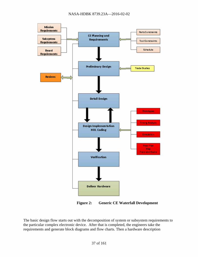
Like any other engineering discipline, the design and development life cycle for complex electronics can follow any lifecycle methodology. In a typical design (or activity), the requirements are flowed down from the system requirements. Development may follow a waterfall, iterative, evolutionary, spiral, or other development methodology. Regardless of the development (design) life cycle, the processes of determining the requirements, creating the design, implementing the design, and verifying the implementation are all included. Since it is easy to show graphically, this handbook will use a modified waterfall life cycle as a generic life cycle to match what is used in the Programmable Logic Devices Handbook.
Like any other engineering discipline, the design and development life cycle for complex electronics can follow any lifecycle methodology. Some of the steps vary from those familiar to software developers. Figure 2 depicts the development process for complex electronics. Based on the size of the project, the Preliminary and Detailed design phases can be combined.
NASA-HDBK 8739.23A—2016-02-02
37 of 161
Figure 2: Generic CE Waterfall Development
The basic design flow starts out with the decomposition of system or subsystem requirements to the particular complex electronic device. After that is completed, the engineers take the requirements and generate block diagrams and flow charts. Then a hardware description

NASA-HDBK 8739.23A—2016-02-02
38 of 161
language is used to create the design (implementation). The design has to be “compiled” for the device (design synthesis). Synthesis is more complicated than just running a compiler. During synthesis, the design is mapped to the logic gates of the device. Simulations are used to verify the design is correct and can meet the requirements and performance goals.
The implementation of complex electronics involves one more level in the mapping of the logic (design) to the chip. The placement of the logic blocks within the chip, and the routing between blocks, are some of the processes that occur during implementation. This process is loosely comparable to the linking step in software, where the compiled program is configured for the software environment in which it will operate. At the end of the implementation phase, the final step is to “burn” or program the device.
Even though the simulation occurring before the design is committed to hardware can find most defects, the actual hardware device needs to be tested in the circuit. Simulation includes simulated environment, both with realistic physical and software challenges emulating the in-use environment worst cases. Real signals are applied, and the real output is tested. Design Engineers usually cannot get the degree of testing with in-circuit verification which can be done with simulation, because inputting out-of-range signals might be difficult, access to the hardware pins might not be possible, and, in real projects, demand for the hardware may constrain functional testing. However, functional testing in a variety of conditions is an important verification step. Errors in the silicon chip are possible. Sometimes the actual environment acts differently than expected and can influence how the device works.
During the implementation phase, the tasks of the assurance engineers (quality/hardware/software) can vary between projects with some only taking a look at the system at a high level, and then verifying that the final device matches the design and that it was programmed according to a defined process. NASA is looking at how to adequately verify the complex electronics device. More information is provided in Section 6.4. Table 2 gives a comparison of the development process for software and complex electronics.

NASA-HDBK 8739.23A—2016-02-02
39 of 161
Table 2: CE vs. SW Development Phases
Software Complex Electronics
Requirements
Software requirements flow down from system and subsystem requirements.
Planning &Requirements
Requirements for complex electronics flow down from system and subsystem requirements.
Design
Architectural and detailed designs are created, using UML, flow diagrams, and other tools.
Preliminary Design
Block and data flow diagrams are created that serve as the design architecture.
Detailed Design
A more detailed design is generated based on the requirements and architecture. This phase iterates with the design implementation phase to further modify and/or expand the design until it meets all requirements.
Code
The design is translated (manually or automatically) into a programming language (code), and then compiled into an executable module.
Design Implementation
Coding in HDL is completed. Design simulation, synthesis, place and route (PnR), and timing analyses are performed. The design is tested on a development board and/or hardware resembling the final system. This phase can iterate with Detailed Design as needed.
Test
The software is tested in individual units and as part of the system. Testing may involve additional software that simulates inputs to the software under test.
Verification
Testing occurs during the preliminary, detailed and implementation phases, in the form of simulations. Both expected (valid) and unexpected inputs are tested. Once the device is created, it is tested as part of its subsystem (in-circuit testing). Verification confirms all requirements for the PLD have been implemented.
Assurance effort should be based on the classification effort assigned to the PLD being developed. It can range from no in-process support to complete support for Safety Critical designs. Figure 3 below shows the potential reviews that may be performed. Reviews will be

NASA-HDBK 8739.23A—2016-02-02
40 of 161
completed by the appropriate qualified people and could include SMEs (Subject Matter Experts) from outside the project.
Figure 3: Quality Assurance Support for PLD Development

NASA-HDBK 8739.23A—2016-02-02
41 of 161
Table 3 below shows the documentation that can be developed based on the development milestones of the PLD.
Table 3: PLD Artifacts for Each Milestone
Product SRR SDR PDR CDR TRR SAR
Development Plan P B U U
Schedule D P B U U
Requirements Specification D P B U U
Verification Plan D P B U
Design Specification P P B U
ICD D P B
Test Procedures B
Test Reports F
Key:
D – Draft P – Preliminary B – Baselined U – Updated F– Final
6.3 Criticality Assessment
If the PLD meets any of the following criteria it should be considered safety critical.
The PLD provides the data needed to make a safety critical decision,
The PLD controls a hazard,
The PLD monitors a hazard,
The PLD can cause a hazard, or
The PLD is used to mitigate a hazard.
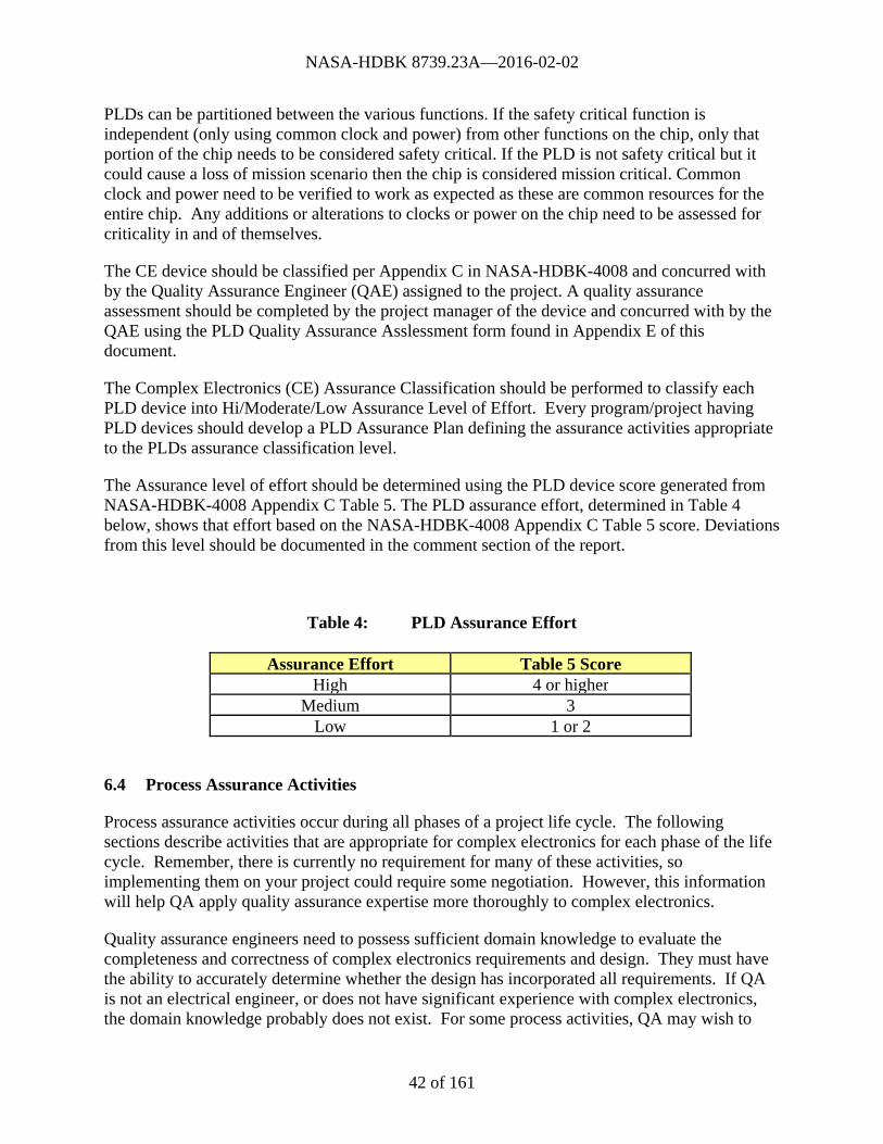
NASA-HDBK 8739.23A—2016-02-02
42 of 161
PLDs can be partitioned between the various functions. If the safety critical function is independent (only using common clock and power) from other functions on the chip, only that portion of the chip needs to be considered safety critical. If the PLD is not safety critical but it could cause a loss of mission scenario then the chip is considered mission critical. Common clock and power need to be verified to work as expected as these are common resources for the entire chip. Any additions or alterations to clocks or power on the chip need to be assessed for criticality in and of themselves.
The CE device should be classified per Appendix C in NASA-HDBK-4008 and concurred with by the Quality Assurance Engineer (QAE) assigned to the project. A quality assurance assessment should be completed by the project manager of the device and concurred with by the QAE using the PLD Quality Assurance Asslessment form found in Appendix E of this document.
The Complex Electronics (CE) Assurance Classification should be performed to classify each PLD device into Hi/Moderate/Low Assurance Level of Effort. Every program/project having PLD devices should develop a PLD Assurance Plan defining the assurance activities appropriate to the PLDs assurance classification level.
The Assurance level of effort should be determined using the PLD device score generated from NASA-HDBK-4008 Appendix C Table 5. The PLD assurance effort, determined in Table 4 below, shows that effort based on the NASA-HDBK-4008 Appendix C Table 5 score. Deviations from this level should be documented in the comment section of the report.
Table 4: PLD Assurance Effort
Assurance Effort Table 5 Score High 4 or higher
Medium 3Low 1 or 2
6.4 Process Assurance Activities
Process assurance activities occur during all phases of a project life cycle. The following sections describe activities that are appropriate for complex electronics for each phase of the life cycle. Remember, there is currently no requirement for many of these activities, so implementing them on your project could require some negotiation. However, this information will help QA apply quality assurance expertise more thoroughly to complex electronics.
Quality assurance engineers need to possess sufficient domain knowledge to evaluate the completeness and correctness of complex electronics requirements and design. They must have the ability to accurately determine whether the design has incorporated all requirements. If QA is not an electrical engineer, or does not have significant experience with complex electronics, the domain knowledge probably does not exist. For some process activities, QA may wish to

NASA-HDBK 8739.23A—2016-02-02
43 of 161
find an expert (either in the assurance arena or in engineering) to help QA or to independently perform an analysis or evaluation. The most important aspect of assurance is evaluation by someone other than the designer, but not all evaluations have to be performed by the quality assurance engineer.
As QA performs assurance activities on complex electronics, keep in mind some quality criteria. These criteria will help judge the status of the product or process.
Correctness. The extent to which a device fulfills its specifications.
Efficiency. Use of resources; performance characteristics.
Flexibility. Ease of making changes if required.
Interoperability. Effort required coupling the system to another system.
Maintainability. Effort required locating and fixing a fault in the program within its operating environment.
Reliability. Ability not to fail, including in off-nominal environments.
Testability. Ease of testing the device to ensure it is error-free and meets its requirements.
6.5 Planning and Requirements Phase
6.5.1 Planning
The planning phase is where the project does the initial assessment of the work required to develop the device. A PLD rating assessed is performed using the Engineering PLD Handbook. This rating, along with the planned artifacts, is documented in the PLD Development and Management Plan.
6.5.1.1 PLD Development and Management Plan
A good development plan will include the following items:
The assessment rating of the PLD(s),
The development tools being used,
Definition of metrics to be collected,
System safety considerations,
Configuration management,
When and how bugs will be tracked,
Reviews to be held,
Risk management,
Required team training, and

NASA-HDBK 8739.23A—2016-02-02
44 of 161
The deliverables being developed.
PLDs, especially small ones, may not have a separate PLD Development and Management Plan. It may be part of the avionics development document.
6.5.1.2 Tool Selection
The first step in creating a design for complex electronics is to choose how the designer will enter (capture) the design. Early chip designs were primarily performed with schematic capture. Schematic capture (also called schematic entry) creates the electronic diagram, or schematic, of the electronic circuit. This is usually done interactively with the help of a schematic capture tool also known as a schematic editor.
While schematic capture works fine for simple designs, complex electronics almost always require the use of a hardware description language (HDL). HDLs are languages used for formal description of electronic circuits. These languages describe the operation, design, and simulation tests of the circuit. HDLs show several aspects of the design, including the temporal behavior and spatial structure. One major difference between HDLs and software languages is the aspect of timing and concurrency. Software runs in a sequential manner while a PLD has multiple events happening at the same time.
One very nice aspect of HDLs is that they can be used as an “executable specification” to simulate the circuit. Simulation software can be part of the tool suite provided by the vendor or a third-party program. Simulators read the HDL “code” and model the structure and flow of the circuit through time.
The two primary description languages are VHDL and Verilog. A later section in this handbook will discuss these two languages in greater detail. Older HDLs, such as ABEL and CUPL, are still in use, especially for simple designs. Another trend in hardware description languages is to add hardware-specific elements to software programming languages. JHDL is implemented on top of the Java language. SystemC adds hardware constructs as a C++ class library. Still, VHDL and Verilog are by far the most common hardware description languages in use.
Regardless of the method chosen to input the design (a hardware description language or schematic capture), a software tool (or tool suite) is required. Unlike most software development efforts, where tools other than editors, compilers, development environments, and version management software are rarely used, electronics designers require, and use, fairly sophisticated tools. All major complex electronics vendors offer design tools optimized for their devices at a relatively low cost. Third-party tools are common and can provide additional capability. These tools are also often quite expensive. However, because the boundaries between design entry, simulation, synthesis, and place-and-route are well defined, designers can use a variety of tools from different vendors.
A tool suite may include the following types of tools:
HDL capture and design environment,
HDL simulator,

NASA-HDBK 8739.23A—2016-02-02
45 of 161
Logic synthesis (this is a critically important tool), or
Layout (physical synthesis).
6.5.1.3 Design Views
Complex electronic devices are designed at several levels, and with several “views,” or ways of looking at the device. Software shares some of these views (e.g., the behavioral/functional view and the structural view), though software is not concerned with physical layouts. Each view for the device can be refined at various levels of representation. The Y diagram in Figure 4 shows how all these views and levels are related.
Figure 4: Complex Electronics Design Views
Modern design approaches for complex electronics focus on the behavioral/functional aspects of the devices and use sophisticated tools to create the appropriate structural and physical aspects of the design. Earlier design approaches required much more manipulation at lower levels of the device circuit. With increasing complexity of the devices, the design aspects have been advanced into a more abstract domain, and the work of converting the design into a usable circuit is left to the tools. This abstraction allows the designer and others to understand how the device functions within the context of the system.
A specification in a hardware description language consists of one or more modules. The top-level module specifies a closed system containing both test data and hardware models.
Behavioral/Functional
Physical/Geometrical
Structural
Algorithmic/System level
Circuit level
Logic level
Register-Transfer level
System spec/algorithm
Register Transfer spec/ Finite State Machine
Module Description
Boolean Equation
Processor, Memory
Register, ALU
Gate, Flip-flop, switch
Transistor
Chip floorplan
Module Placement
Mask
Cell Layout

NASA-HDBK 8739.23A—2016-02-02
46 of 161
Component modules normally have input and output ports. Events on the input ports cause changes on the outputs. Events can be either changes in the values of wire variables (i.e., combinational variables) or in the values of register variables, or can be explicitly generated abstract events. Modules can represent pieces of hardware ranging from simple gates to complete systems (e.g., microprocessors), and they can be specified either behaviorally or structurally, or by a combination of the two.
A behavioral specification defines the behavior of a digital system (module) using traditional programming language constructs (e.g., IFs, assignment statements). This description of a complex electronic device divides the device (chip) into several functional blocks that are interconnected. A hardware description language is used to describe the behavior of each block. Functional blocks can be a finite state machine, a set of registers and transfer functions, or even a set of other interconnected functional blocks.
A structural specification expresses the behavior of a digital system (module) as a hierarchical interconnection of subordinate modules. The components at the bottom of the hierarchy are either primitives or are specified behaviorally. It is in the structural specification that individual inputs and outputs are defined.
6.5.1.4 Assurance Activities
The initial stage of a project or system is the time when many decisions are made that will affect the project months or years down the road. While the technical decisions are driven by the results of systems engineering trade-off studies, the assurance decisions are driven by a combination of:
Requirements and standards,
What are the NASA, Center, and other quality assurance standards that the project must follow?
Project management support,
The level of assurance is directly proportional to the amount of support that project management supplies. When quality assurance is perceived as a useful tool to help develop a functional system within the project constraints, quality assurance engineers are given adequate funds and personnel to do a thorough job. If the project manager deems quality assurance an annoyance, then the ability of the quality assurance engineer to implement an effective program is hampered.
Effectiveness of the assurance organization, and
An assurance organization that has a track record of working with projects to develop tailored and effective assurance plans and processes will be more likely to gain project support in implementing new assurance activities. Conversely, an organization that does not have a good working relationship with projects will make it much more difficult for the assigned quality assurance engineer to persuade the project to consider any additional assurance activities for complex electronics.

NASA-HDBK 8739.23A—2016-02-02
47 of 161
Knowledge and experience of the assurance professional.
The assurance professional has to be proactive in implementing quality assurance activities, especially for new areas such as complex electronics. If the quality assurance engineer lacks knowledge and experience, the necessary assurance infrastructure may not be put in place.
Quality assurance is involved in project planning activities through:
Classification of the PLD per section 6.3 in this handbook;
Using Table 6 in NASA-HDBK-4008 to determine the list of recommended items per the project’s PLD classification;
Creation of a Quality Assurance Plan outlining the work to be performed by the quality assurance engineer throughout the project life cycle;
Assessment of the project plans, including the management and development plans for electronics, for completeness, correctness, and other quality attributes; and
Assuring the project produces the required plans.
The plans a project will produce depend on the NASA and Center requirements and the project complexity and safety-criticality. The content of the plans often varies between projects, with one project combining several documents and others producing separate plans. Do not get hung up about which plan is which, but review the project plans for how they will address complex electronics. If they do not address the issues at all, encourage the project manager or the design engineer to informally document the information.
Here are some areas the project plans should address regarding complex electronics:
How will the complex electronics life cycle interface with the project life cycle? In describing the life cycle, does the document discuss transition criteria between phases, and how to return to previous phases if problems are found?
Are they following the guidelines found in the Engineering PLD Handbook?
What is the hardware design process?
What activities will be performed as part of the process?
What design environment (e.g., tools) will be used?
If deviation from established plans becomes necessary, what is the process for doing this? For example, how will changes be approved by all interested parties?
How will the design for complex electronics and any associated data be included in the configuration management system?
Does the project have a defined process to review and approve revisions to the design?

NASA-HDBK 8739.23A—2016-02-02
48 of 161
Are the plans written at least in draft form before the life cycle phase in which they will be used?
The Development or Test Plan should include activities for reviewing the requirements and design, witnessing or performing testing, and performing other product verification steps.
Risk management is an important tool that projects can use in reducing the probability or impact of risks. Complex electronics has some fluidity of the requirements. Additionally, CE have integration issues (often as a result of interface problems), and the need to create a complex program within a defined period of time. These types of issues are ideal for risk management mitigation. Programmatic questions to ask include:
Is the design team experienced or has the project been customized to take into account the experience of the team?
Is there a design guideline document defining design rules? Is the team using guidelines from the Engineering PLD handbook?
Has the team created a naming convention or style guide?
How are detected error conditions handled?
Is the design maintained in a version control or configuration management system?
Has anyone looked at what standards may be applicable (Center, NASA, other)?
Are all needed parts of the same revision and of sufficient quantity for intended use?
6.5.2 Requirements
Creating complex electronics begins where all systems and subsystems begin - with defining the requirements for the device. Without good requirements, the most elegant design or implementation could fail to meet the original need. Designing and implementing complex electronics occurs within the context of the larger system.
Requirements for the complex electronics are driven by the system they are a part of and the environment in which they will be used. A simple home appliance places fewer demands (requirements) on a device than a sophisticated satellite application will. Because these devices are hardware, the process of complex electronics design involves looking at both the chip capabilities and constraints (e.g., How many gates does it have? How much power does it need?) and how the design works with and against those constraints and capabilities.
The first step in the design process is to understand (and document) the functions the complex electronics device must perform and the constraints under which it operates. The act of

NASA-HDBK 8739.23A—2016-02-02
49 of 161
documenting the requirements has some useful effects that actually can save time in the long run. Benefits include:
The design team thinks through the issues and reaches agreement. Some issues are well understood at a high level, but raise additional questions when working at the hardware level.
Interfaces to other areas (software, other hardware) are defined and available for review by all affected parties.
Non-engineers can understand what the chip or device is supposed to do.
If the trade-offs and rationales are documented, as well as the requirements, future design changes will require less impact assessment.
The requirements can be reviewed to assure they provide measurable, testable criteria.
Requirements traceability into the design and implementation can be performed – which is vital in mission or safety-critical applications.
Allows simultaneously preparing the verification/validation method for each requirement.
A good requirements specification for complex electronics will contain:
A description of how the device fits into the larger system. A block diagram is very helpful.
A description and list of all the major functions the device will perform. A block and/or flow diagram can be used to show this information.
Reference to Interface Control Document (ICD) for board device, or equivelant, which contains a description of the device and interfaces, such as:
Chip physical information (size, type, number of pins, etc.), and
I/O pin mapping and description (output drive capability, input threshold level).
Reference to Design Specification containing:
Clock cycle time,
High-level estimates and goals,
Power consumption target,
Constraints on the device,
Other requirements or criteria the device must implement, and
Design-related choices (may be in a development management plan):
Tools to be used at all stages of development.

NASA-HDBK 8739.23A—2016-02-02
50 of 161
Hardware Description Language chosen.
PLDs, especially small ones, may not have a separate requirements documents. The requirements document may be part of the avionics requirements document with a distinguishing mark.
6.5.3 Assurance Roles
What role does quality assurance play in verifying the requirementsspecification for complex electronics? During the requirements development process, system requirements are allocated to various subsystems and parts, including complex electronics. These requirements need to be documented (in a separate specification for complex electronics or as part of another requirements specification document).
Many assurance engineers, regardless of their specialty, have little understanding of the complexities of these devices. Any review or evaluation will be to the level of knowledge of the assurance engineer. Hence, the importance of using SMEs (Subject Matter Experts). Conversely, the assurance engineer brings a broader view, disciplines and structure important to success.
Hardware Quality Assurance Engineers are the primary assurance people to deal with complex electronics. Hardware quality assurance engineers with a background in electronics will evaluate the requirements for the complex electronic device for accuracy, completeness, and compatibility with the rest of the system.
System Safety Engineers will be involved in the review when the devices are part of safety-critical systems or are used as controls or mitigations for hazards. As with hardware quality assurance, system safety engineers usually do not have an in-depth understanding of complex electronics.
Software Quality Assurance Engineers at NASA are involved with complex electronics when software will be running on the device. They will ensure any software running on an embedded processor follows NPR 7150.2, NASA Software Engineering, requirements. Significant education or training is required to be able to adequately review the requirements and specification for complex electronics at a detailed level. However, this handbook explains how to review specifications for complex electronics at a high-level and to look for the following:
Problems with interfaces to the software running on the system, and
Additional constraints that may not be included in the specification, based on software requirements.
Overall, the quality assurance activity reviews the requirements for the complex electronic devices and verify that they:
Include all requirements appropriate for the complex electronics (i.e., verify the allocation was complete);

NASA-HDBK 8739.23A—2016-02-02
51 of 161
Identify any requirements that are safety-related or mission critical by working with system safety and engineering;
Identify design constraints for the complex electronics;
Are clear, concise, and verifiable;
Are traceable to a higher level document or are noted as derived requirements; and
Can be met by the PLD to be used.
It is important that the requirements are as clear as possible, because many problems found later in system design can be traced back to ambiguous or incorrect requirements. Requirements for complex electronics should be more than just a cut-and-paste from the system requirements specification. They should be decomposed to the appropriate level of detail, and provide enough information such that a designer can create the device. Each requirement should levy just one obligation on the hardware design.
Activities for the requirements verification for complex electronics must be specified in the verification plan. If a verification method cannot be determined, that indicates that the requirement is flawed and needs to be fixed.
For safety-critical or mission-critical devices, formal methods might be used as a verification tool. The requirements can be defined using a special language that allows mathematical proofs to be generated showing the device will not violate certain properties. Formal methods can be applied at only the requirements level (to make sure they are correct), or can be used to verify the design when it is generated. Most projects will not use formal methods.Table 5 shows potential verification activities performed during the requirements phase.
Table 5: Requirement Verification Activities
Verification activity Performed by Evaluate requirements for the complex electronics Quality assurance engineer,
Systems safety engineer
Safety assessment System safety engineer
Requirements review All
Identification of applicable standards Quality assurance engineer, safety engineer, design engineer
Formal methods Knowledgeable practitioner

NASA-HDBK 8739.23A—2016-02-02
52 of 161
6.6 Preliminary Design Phase
6.6.1 Roles of the Engineering Design Team
During the preliminary design phase the architecture for the PLD is created. The top-level design is generated using the architecture from the requirements in the form of block diagrams. Preliminary data flow diagrams are created and the interfaces to the PCB (Printed Circuit Board) defined. A description of all hardware and software interfaces is created. An architecture review is normally held at the end of this phase to ensure all the requirements have been addressed. Smaller designs can combine the preliminary and detailed design phase activities.
6.6.2 Assurance Roles
At the preliminary design phase, Quality Assurance and System Safety can participate in architecture and high level design reviews.
Hardware Quality Assurance Engineers will evaluate the design for the complex electronic device against the requirements. For many projects, especially when hardware quality assurance engineers have little exposure to, or understanding of, complex electronics, no evaluation will be performed.
System Safety Engineers will review the design of the devices when they are part of safety-critical systems. Since few system safety engineers are experts in complex electronics, they will work with the designer or hardware quality assurance engineers to evaluate the design from a safety perspective.
Software Quality Assurance Engineers will participate in the reviews when software will be running in a processor on the chip or interfacing with the device.
Potential verifications that will occur during the preliminary and detailed design phases are listed in Table 6 below.
Table 6: Design Verification Activities
Verification activity Performed by Evaluate block diagrams & flow charts Quality assurance engineers & design
engineer(s)
Architecture Review Independent design engineer
Safety assessment System safety engineer & design engineer(s)
Design reviews All (If safety critical (QA recommended))
IDD (Interface Design Document) for PCB and Software
All
NASA-HDBK 8739.23A—2016-02-02
53 of 161
6.7 Detailed Design Phase
During the detailed design phase the block diagrams from the Preliminary Design Phase are used to generate a detailed design based on the requirements and architecture. This phase iterates with the Implementation Phase until all requirements are met.
6.7.1 Roles of the Engineering Design Team
During the detailed design phase the engineer uses the block diagrams and flow charts developed in the preliminary design phase to generate the design specification. Detailed design information, such as detailed block diagrams and timing diagrams are developed. The information developed in this phase is used for capturing the design in HDL during the design implementation phase.
6.7.2 Assurance Roles
At the Detailed Design phase, assurance and safety engineers are not always involved except in the case of safety or mission critical devices. A hardware assurance engineer might participate in the various design reviews. Assurance activities will seek to answer these questions:
Does the design meet the specification?
Is the design partitioned into logical components?
Does the designer provide enough background information to understand what the device is supposed to do?
Is there anything in the design that conflicts with other subsystem or system components?
Do the design interfaces (input and output signals) match the interfaces as specified by the other components?
Were the special pins on each device (e.g., mode pin on FPGA, JTAG pins, no-connect pins) verified that each is used properly?
The Engineering PLD Handbook Appendix B.3 has the checklist that can be used by engineering and assurance. This provides additional items to consider.
6.8 Design Implementation Phase
During the design implementation phase the block diagrams and flow charts from the detailed design phase are used to generate HDL based on the requirements and architecture selected. The HDL code can be simulated in a test bench and its behavior can be observed. This is an important verification activity that is usually performed solely by the design engineer. Quality assurance engineers may review the simulation plans (if they are produced) or results, and for critical devices they may witness some of the simulation runs. Table 7 below shows the verification activities performed during design implementation.

NASA-HDBK 8739.23A—2016-02-02
54 of 161
Table 7: Design Implementation Verification Activities
Verification activity Performed by Evaluate design (HDL) against requirements Quality assurance engineer or SME
Functional Simulation Design engineer
Safety assessment System safety engineer & Design engineer(s)
Design review (e.g., CDR, peer review) All
Functional simulation involves emulating the functionality of a device to determine it is working per the specification and it will produce correct results. This type of simulation is good at finding errors or bugs in the design. Functional simulation is also used after the design synthesis step where the gate-level design is simulated.
One or more engineers who can assess the design should review the HDL code. A good reviewer has to understand the system within which the device will operate, know the HDL language being used, and be able to compare what the device is designed to do against its requirements.
For very complex or safety-critical devices, assurance engineers or Independent Verification and Validation (IV&V) practitioners may be called in to review the design. This phase iterates until all requirements are met. The various activities that occur and the items used during this phase are discussed below.
6.8.1 Synthesis
Design synthesis is the process that takes the higher-level designs and optimally translates them to a gate-level design which can be mapped to the logic blocks in a complex electronic device. Unlike software, which executes sequentially, the elements of a complex electronic chip will execute in parallel, with specific timing requirements. However, in general, synthesis is a form of compiling- translating the readable language into instructions that are implemented in the integrated circuit. The synthesis step transforms the behavioral and structural specifications into an optimized netlist of gates. The netlist is a description of the various logic gates in the design and how they are interconnected. During synthesis, the designer can optimize parameters and constraints in the final chip.
Synthesis is performed almost exclusively by a software tool. Modern synthesis tools do an excellent job of optimizing complex designs, so designers do not need to manually perform that task.
6.8.2 Simulation
Simulation is one of the primary ways the design synthesis process is verified. In almost all projects, the design engineer is the one who generates the test bench, defines the simulation runs, and performs the simulations. Quality assurance engineers are rarely involved, other than to

NASA-HDBK 8739.23A—2016-02-02
55 of 161
perhaps verify the simulations were performed. However, it is important to look at the design of the test bench and the simulation tests to make sure they are complete enough. This is the time to find errors or mistaken assumptions - not when the designer is integrating the complex electronics with other areas of the system.
Understanding how the complex electronics will operate when given invalid input is very important in verifying the devices. The real world is messy, and noisy signals or broken interfaced hardware are unfortunately common. Simulation is a great way to perform fault injection testing by inputting signals that are out of range, whose timing is not correct, that have ringing or other signal problems, or that are noisy. Encouraging this type of testing, and helping to identify the likely types of faults, is one way quality assurance personnel can actively participate in the verification of complex electronics.
Simulation is used in the design of complex electronics at several levels. One very nice aspect of hardware description languages is they are “executable,” and simulators that can run the code are very common. Simulators are usually part of the tool suite provided by the vendor of the complex electronic device (e.g., FPGA).
After design entry, the design is simulated at the register-transfer level (i.e., the HDL code). Simulation at this level is very fast, allowing the designer to implement many simulations to fully understand how the device will operate. Simulation can be used to help optimize the design and refine the logic, though designers need to be careful not to use it in an undisciplined code-and-fix mode. Simulation of the HDL code will look at signals and variables to check their value, trace functions and procedures, and will use breakpoints to check the status of the device at specific events. This process is very similar to using a software debugger. One caveat with simulation at this level of design is that some properties are not yet defined, such as timing and resource usage.
After design synthesis, but before physical implementation, functional simulation can be used to help verify the design. The goal of functional simulation is to ensure the logic of the design does what is required, per the specification, and that it produces the correct results. This type of simulation can help get as many bugs out of the device as possible. If any errors are discovered, then the implementation step is revisited and necessary required changes are made, leading to a successful simulation. This simulation is rarely performed due to expense and resource requirements.
After the design has been implemented, but before the device is actually programmed, a final simulation with full timing information can be performed. The placement and routing process will determine any delays and other timing information, which are back-annotated to the gate-level netlist. This simulation is a much longer process, because of the timing aspects, and is rarely done. A static timing analysis might be substituted for the timing simulation. Static timing analysis calculates the timing of combinational paths between registers and compares it against the designer’s timing constraints.

NASA-HDBK 8739.23A—2016-02-02
56 of 161
6.8.3 Test Benches
Test benches for complex electronics are not made of wood or metal, but of Verilog or VHDL code. They are special programs designed to test complex electronics designs. While simulators can verify simple designs, more complex designs require a test bench to adequately verify the design.
A test bench is a HDL design created which can load the circuit, apply stimulus to its inputs (including defining multiple clocks), and check the outputs for correctness. Because the test bench is a program the designer writes, he has control over how the circuit is built and simulated. In addition to the above capabilities, a test bench can provide behavioral or structural models for everything on the PC board. In this way, it enables the designer to simulate the entire system including the complex electronics design(s) as well as external bus interfaces, external memories, etc. An engineer can design the test benches to automatically check important data conditions and to report any errors to a command window.
Comprehensive, upfront verification is critical to the success of a design project, and test benches should be created as the design engineer starts to design the device. A HDL test bench/simulator can become the primary design development tool. When simulation is used right at the start of the project, the designer will have a much easier time with synthesis, and will spend far less time re-running time-intensive processes, such as place-and-route tools and other synthesis-related software.
Test benches can be simple, applying a sequence of inputs to the circuit over time. They can also be quite complex, perhaps even reading test data from a disk file and writing test results to the screen and to a report file. A comprehensive test bench can, in fact, be more complex and lengthy (and take longer to develop) than the circuit being tested.
Depending on needs (and whether timing information related to the target device technology is available), the designer may develop one or more test benches to:
Verify the design functionally (with no delays),
Check your assumptions about timing relationships (using estimates or unit delays), and
Simulate with annotated post-route timing information to verify that the circuit will operate in-system at speed.
A typical VHDL or Verilog test bench is composed of three main elements:
Stimulus Generator - drives the unit under test with certain signal conditions (correct and incorrect values, minimum and maximum delays, fault conditions, etc.);
Unit Under Test - represents the device undergoing test or verification; and
Checker- automatically checks and reports any errors encountered during the simulation run. Compares model responses with the expected results.

NASA-HDBK 8739.23A—2016-02-02
57 of 161
Test benches are created by human beings, often by the designer, and are subject to faults and failings like any human endeavor. If the logic of the test bench is incorrect, or if a particular stimulus is not defined, then the end result of the tests may not show an actual error. This scenario is something to keep in mind if QA is called on to review verifications for a piece of complex electronics. QA cannot assume that the test bench accurately and completely tested the device. Therfore it is prudent to have another qualified engineer other than the design engineer develop the test bench and perform testing of code, especially if the device will be used in a safety-critical application.
6.8.4 Implement the Design
Once a design has been created, simulated, and synthesized, the next step is implementation of the design in the particular complex electronics device. In software, implementation is usually translating the design into source code and compiling it. In complex electronics design, implementation is where the design meets the silicon - the higher-level design is converted into a chip layout.
The implementation process uses the tools supplied by the device (e.g., FPGA) vendor. The functions previously defined in the design have to be matched to the available blocks, gates, and other logic elements on the chip. The following steps are rarely done manually. Some basic steps in implementing a design are:
Floorplanning,
Translation,
Mapping, and
Place and Route.
The exact order of a step (or even the name a step/process is given) varies across different groups, companies, and documents. Thus, do not take the information in this handbook as the only correct way to do things. However, the concepts presented here are common across the industry and will be implemented to some extent in all programs - perhaps as part of an automated tool or under a different name. Being familiar with the concepts will help QA “speak the language” when talking with a design engineer working with complex electronics.
6.8.4.1 Floorplanning
Floorplanning is the process of identifying structures that should be placed close together, and allocating space for them. In designing complex electronics, there are multiple goals that must be met, and the goals often conflict. Finding the best balance between the various goals and requirements is something of an art. Some goals are:
Minimizing space on the chip (allows choice of less costly chips),
Meeting or exceeding required performance, and
Placing everything close to everything else to minimize transmission time in the signal paths.

NASA-HDBK 8739.23A—2016-02-02
58 of 161
Floorplanning does not have to be performed by the designer for many designs/chips. Most tool suites will perform this step as part of the automated sequence that takes the design and implements it in the chip. However, if the designer is creating an ASIC, needs the absolute best timing possible, or is trying to cram a large design into a not-so-large chip, active floorplaning may be need.
As a general rule, data-path sections benefit most from floorplanning, and random logic, state machines and other non-structured logic can be safely left to the placer section of the place and route software. Data paths are typically the areas of your design where multiple bits are processed in parallel with each bit being modified the same way with some possible influence from adjacent bits. Example structures that make up data paths are adders, subtractors, counters, registers, and muxes.
6.8.4.2 Translation
Translation involves converting the results of the synthesis process to the format supported internally by the vendor’s place-and-route tools. The incoming netlist is checked for adherence to design rules and is then optimized for the chip.For example, a certain amount of delay may be necessary when accessing an outside element like a sensor. This delay can be included as a constraint during the translation process. Other constraints may be power consumption and signal timing.
Translation may also be referred to as compilation or compiling. This process is automatic, but it takes some wading through the reports produced by the tool to verify the translation/compile was correct. An intelligent post-processor, rather than the designer (or the quality assurance engineer), should find syntax and binding errors - otherwise the designer/QA will have to do this for each design modification. However, user input to the tools does have an effect on the output. For example, translation tools behave very differently given a common set of constraints. These timing-driven tools perform complex trade-offs to achieve the timing constraint specified, including adding extra parallel logic to paths where there is negative timing slack, or optimizing a critical path at the expense of a non-critical one. When the designer over constrains a design, the tool sees many, many paths that does not meet timing and can generate lots of extra logic in a futile attempt to make all of them hit the timing goals. This can result in a much larger design with reduced overall timing performance. In a timing-driven tool, the idea is to give the tool the real timing specifications, and let it work to meet that goal. Once the performance goal has been met, the tool will start optimizing for less area which translates to cost savings in your device. This can produce an even faster design because routing delays can be reduced by having less logic in non-timing-critical areas.
6.8.4.3 Mapping
Mapping takes the logic blocks and determines what logic gates and interconnections on the device should be used to implement those blocks. During the mapping step, the functions within the device (such as counters, registers, or adders) are aligned with the logic resources of the chip. The exact process is device dependent. For example, FPGAs have look-up tables that perform logic operations. The mapping tool (part of the vendor’s tool suite) collects the gates defined by the netlist into groups that will fit within the look-up tables.

NASA-HDBK 8739.23A—2016-02-02
59 of 161
6.8.4.4 Place and Route
Place and Route is the process of placing the logic blocks in the best spots on the chip to achieve efficient routing. Items that the place and route tool will look at include routing length (how far does a signal have to travel), track congestion (how many signals are coming into or out of an area), and path delays. While vendor-supplied tools usually perform the process automatically, the designer can specify some parameters and constraints that the final layout has to meet, including the initial placement of the cells, a position for each physical connector, and a form factor.
6.8.5 Programming the Device
Once the design is successfully verified and found to meet timing and performance requirements, the final step is to actually program the device. At the completion of placement and routing, a binary programming file is created and used to configure the device. The process of programming is usually dependent on the type of memory used to store the device configuration and on the device type (e.g., FPGA or ASIC). Some factors in device implementation to consider are described below.
6.8.6 Assurance Roles During Implementation
During the implementation phase, the complex electronics functionality and structure are defined in a hardware description language (HDL). The HDL “program” is actually a model of the complex device, and can be run (simulated) and tested.
Prior to the start of the implementation phase, several process assurance activities should have been performed:
Tools. Review selected tools for applicability to the design process. Check the tool vendor web site and other sources for known tool defects or operational workarounds.
Design Process. Make sure a disciplined design process is in place, and the design engineer is willing to follow it. Negotiate as necessary.
Configuration Management. Make sure the HDL code and other design information is configuration managed. The level of formality depends on status of design (e.g., informal version control prior to baseline, formal change control after baselining).
Design and Coding Standards. Ensure the design team is using a design and coding standard. This standard will define the basic design philosophy and specify aspects of the HDL program structure. Even if only one engineer is designing the device, a standard 1) helps ensure the HDL program is understandable by others (and the design engineer, six months down the road) and 2) provides a way to capture and incorporate best practices in the design process.

NASA-HDBK 8739.23A—2016-02-02
60 of 161
A design and coding standard should include:
Specific HDL coding features and methods that either should be used or should not be used;
Naming conventions for modules, inputs, outputs, etc.; and
Commenting rules defining what types of information to include in comments. One example would be to define a module header that includes comments on the module’s purpose and structure.
At this stage, assurance and safety engineers are involved in multiple ways. The test bench and hardware test cases should be assessed to verify they are correctly testing the device being created. The assurance engineers may be required to witness the programming (“burning”) of the device. Much of the implementation process is performed by automated tools, so if the tools were previously assessed, the results can be accepted without additional review.
Quality Assurance engineers should verify all PLD requirements have been implemented and tested. The hardware engineer and system safety engineer can witness the simulations of the device, and/or assess the test bench created for the simulations. The software assurance engineer might witness the testing of the software running on the embedded processor. The system safety engineer may review the simulation results of any safety controls, monitoring or mitigations.
Assessment of the HDL design should be performed in parallel with the design effort, with intermediate design elements being reviewed, if the project criticality warrants it. Otherwise, the review is normally performed after at least a fairly stable design (if not baselined) is created.
Process assurance activities post-HDL-design includes:
Ensuring the design is reviewed by someone who has enough knowledge to make an expert assessment. This can be another engineer, a quality assurance engineer, or even an outside expert. Another set of eyes will help spot problem areas of the design. This review could be part of a formal inspection or other peer review.
Reviewing the design (behavioral and structural specification in HDL) against the requirements. Are all requirements correctly and completely implemented?
Tracing the requirements into the design elements. The rigor of this tracing should be determined by the safety-criticality and mission-criticality of the device.
Identifying any derived requirements that emerge from the design process. Make sure the rationale for these requirements is captured.
Reviewing the design against the design and coding standard. This is NOT a style check.
Assessing the use of special pins on each device (e.g., mode pin on FPGA, JTAG pins, no-connect pins) and verifying each is used properly.

NASA-HDBK 8739.23A—2016-02-02
61 of 161
Identifying constraints (design, installation, operation) that could affect safety if not followed.
Assessing the simulations performed. Did they cover all the required functionality? Were all modules exercised (not always possible when using IPs)?
Verifying the processes defined in the project plans were followed.
Assuring any design trade-offs done for speed, size, etc., are documented.
Assuring the PLD burn/configuration is witnessed for safety-critical or flight devices.
Assuring a programming procedure that contains the proper information is used if required.
Assuring design “best practices” were used either as guidelines or as requirements.
Assuring the gate output drive capacities were analyzed to determine that none were exceeded.
Assuring the interfaces to other parts were analyzed for input logic level thresholds and maximum input transition times.
Verifying the following questions were answered:
Was a timing analysis performed with the following signals?
Pulse width of each clock, asynchronous set, clear, and load input;
Setup and hold time for all clocked inputs; and
Recovery time for set and clear.
Did the timing analysis also consider the following?
Parallel clocking,
Clock skew,
Timing of analog circuitry,
Minimum propagation delays, and
Worst case timing.
If there is a state machine, assuring it was analyzed for:
Unused states and lock-up,
Simultaneous assertion of flip-flop sets and clears, and
Proper reset conditions.
Are resets of the correct assertion and release voltages, and is the pulse width correct?

NASA-HDBK 8739.23A—2016-02-02
62 of 161
The Engineering PLD Handbook Appendix B.4 has the checklist which can be used by engineering and assurance. This provides additional items to consider.
6.9 Verification
As with any discipline, verification activities do not wait until the complex electronic device is programmed and ready for test. Verification is a parallel set of activities to design and development. Various verification tasks are performed at each phase of the development cycle.
This section of the handbook will answer the questions:
What are the verification steps for complex electronics?
How is verification for complex electronics similar to, and different from, software verification?
Who performs the verifications?
While simulation is used extensively in complex electronic design, testing the actual chip can sometimes be an eye-opening experience. Simulation involves assumptions and compromises that may not match with the real world. Testing the programmed chip - either independently or integrated onto a circuit board - is a necessary step in verifying the design. Final (acceptance) verifications should occur in the real hardware system. This in-circuit verification tests the functionality and timing of the design on the actual chip. Table 8 shows the activities performed during verification.
Table 8: Verification Activities
Verification activity Performed by
In-circuit functional and timing tests Design engineer, may be witnessed by Quality assurance engineers
Sub-system and system tests All
Safety verification All, but reviewed or witnessed by System safety engineer
Secure evidence of compliance, document anomalies and failures
Design engineer, Quality assurance engineers
Ideally, special test software running on a host computer will interface with the device under test through available test ports, such as the JTAG port. This process is similar to in-circuit emulators that run embedded software on the target processor and provide breakpoints and tracing into the actual software instructions. In-circuit verification requires a special build of the device which can change the devices’ operation (i.e. logic, timing).
The more common form of in-circuit testing is to manually run the complex electronics as part of a higher-level assembly to show that it meets all the specified requirements. This subsystem or

NASA-HDBK 8739.23A—2016-02-02
63 of 161
system level test will show functionality at a black-box level, but will not provide a window into the internal functioning of the device.
6.9.1 What Should an Assurance Person Look for?
Process assurance activities for this phase include:
Verifying the defined processes are in place and are being followed correctly.
Verifying the testing strategy has been documented in a plan and/or procedure, and testing occurs according to the plan.
Verifying the planned tests will completely verify the requirements in all reasonably expected situations. This includes verifying the functionality and performance in nominal situations and when other parts of the system have errors. How does the device handle errors it may encounter?
Verifying the planned tests exercise the device as close as possible to the functionality in the sequence and operations that the system will perform on mission with nominal and off-nominal conditions (i.e., test as planned to operate).
Reviewing the verification test plans and procedures to identify any areas where testing is weak. Look for modules only minimally tested, requirements only verified under some circumstances, and other areas where additional testing may be helpful.
Witnessing verification tests (as agreed to in the project plans).
Verifying test results become part of the official project records.
Verifying any anomalies and problems are officially documented.
Review the verification test results to verify no unnoticed anomalies occurred. Sometimes during testing, many events are occurring and an anomaly unrelated to the aspect of the particular test may be missed.
If the complex electronic device is safety-critical, there will be separate safety verifications, usually at the system level.

NASA-HDBK 8739.23A—2016-02-02
64 of 161
7 PLDS DEVELOPED BY A SUPPLIER
Quality assurance of a PLD developed outside of NASA can vary per vendor and by contract. Items to consider when assessing the quality of a vendor PLD should include:
Will the proper design reviews be held?
Will code reviews be held?
What verification activities are planned?
What sort of insight into the development process is authorized?
For a more complete list of items to consider see chapter 13 in the Programmable Logic Device (PLD) Handbook (NASA-HDBK-4007).

NASA-HDBK 8739.23A—2016-02-02
65 of 161
8 METRICS
During the development process it is important to know if the designer is developing a quality product. One way QA can do that is by collecting metrics during the various phases of the development cycle. A metric is defined as “a system of parameters or ways of quantitative and periodic assessment of a process that is to be measured and is usually specialized by the subject area.” Metrics can be used to identify and track trends, problems, productivity, and much more. With complex electronics, metrics must cover both the hardware and software portions of the development cycle.
The two types of metrics used for measurement are called primitive and derived. Primitives are items such as time, number of problems, or lines of code, the base item used to make a decision. A derived metric takes multiple primitives to determine a unit. An example from the software world is errors per lines of code (errors per KLoc). The two primitives used in this measure are the number of software errors and the number of executable lines of code.
Let’s look at some of the primitives available for measurement in the complex electronics development cycle, starting with the number of defects found. This measure can be broken down into when and what type of defect is found. When would specify the development phase or review. Defects could be categorized by type of defect. Examples of these are interface, requirement, and logic or data type. Other categories could include classifying defects as major or minor. Implementation metrics could be collected for total number of functions vs number of functions implemented or tests planned vs. number of tests completed. The important thing to remember when collecting metrics is that they should provide value to the project.
Two measures that can be useful are changes required after first baseline event and variances (deviations anticipated and waivers discovered). Rudimentary forensic work may help determine a metric as happened in many companies in the 1980's when they tracked failure locations and subsequently discovered degradation and failures were traceable to ESD - particularly in development labs where engineers felt ESD practices did not apply to them.
Metrics ought to be constructed to measure without adversely influencing or changing what is being measured. A metric that costs too much time and money can exceed its value.

NASA-HDBK 8739.23A—2016-02-02
66 of 161
9 SUPPORTING PROCESSES
9.1 Configuration Management (CM)
Configuration Management is, unfortunately, often not used for complex electronics design artifacts. The final design is usually saved, but the intermediate development artifacts are under the control of the designer. While formal configuration management might not be used, some form of informal control (e.g., use of a version management system) is recommended. Being able to revert to a previous version of the design is useful when problems are discovered during development. Being able to recreate versions of the design might also be useful to help narrow down when a problem was introduced.
Configuration management should be used as the design is developed. There should be a process in place for changes to be approved prior to the changes being implemented. This control assures:
The configuration of the device is always known, and
Everyone who may be affected by the change has a chance to evaluate the change for impacts to their area of concern.
Some configuration controls are obviously required. One of these is where development is split between two or more engineers. Another is when there is a common file between parties, such as when development is shared with or between Contractors which can result in contract ramifications. When a formal test for acceptance or V&V process has been conducted, the results should be secured and the design "baselined" with a configuration management process.
9.2 Reliability
Most reliability studies look at the hardware failure rates for the devices in a system. While failure of the actual device (e.g., FPGA) can be known, the failures related to design errors or unexpected interactions within the FPGA, once it is programmed, are not easy to determine. Most reliability evaluations ignore software for this very reason.
While there is currently no good way to predictively assess the reliability of a complex electronic design, the fact that there may be design errors should be considered by the reliability engineer. At a minimum, the confidence in the resulting numbers (mean-time-to-failure, system reliability) is lowered.
9.3 Maintenance and Maintainability
If the device will potentially need to be maintained (including reprogramming updates), this issue needs to be considered early in the design of the complex electronics and its supporting circuitry. Some areas to consider are:
Will the device architecture allow for the types of enhancements that can be foreseen?

NASA-HDBK 8739.23A—2016-02-02
67 of 161
Does the design specification provide the information an engineer would need to understand how the product works?
Is the HDL code readable?
Are comments liberal and informative?
Is the necessary physical infrastructure in place to allow reprogramming?
Is access to the reprogramming port, if one is used, available when the system is installed?
Has project secured sufficient quantity of the hardware, including spares, to assure consistency between development items and final use assemblies?
Is this device potentially going to be reprogrammed/updated in-flight?
Does the device have sufficient space available for updates?
Is in-flight programming supported by the device?
Can the device be recovered if the reprogramming fails?

NASA-HDBK 8739.23A—2016-02-02
68 of 161
10 FUTURE TRENDS
10.1 Changes in Complex Electronics Design and Verification
Technology never stands still. Within the realm of complex electronics, devices such as System-on-Chip, FPGAs with embedded microprocessors, and reconfigurable computing all strain the traditional hardware-oriented design and verification approaches. Increasing complexity in designs makes it harder for the designer to conceptualize the design. Several new methods in design and verification of complex electronics hopefully will help improve verification of these devices.
10.1.1 Hardware/software Codesign and Coverification
Since complex electronics is increasingly being combined with software, co-design (and subsequently, co-verification) of the hardware and software is a good idea. Hardware/software co-design is the cooperative design of hardware and software, within a single chip or within a system. One of the goals of co-design is to shorten the time-to-completion while reducing the design effort and costs of the designed products.
In hardware-software co-design, designers consider the trade-off in the way hardware and software components of a system work together to exhibit a specified behavior, given a set of performance goals and technology. This trade-off between hardware and software illustrates the optimization aspect of the co-design problem. Co-design is an interdisciplinary activity, bringing together concepts and ideas from different disciplines (e.g., system-level modeling, hardware design and software design).
Current development methods for designing embedded systems and complex electronics require specification and design of the hardware and software as separate entities. A specification, often incomplete, is authored by the hardware and software designers with inputs from the subsystem engineers. Requirements are developed from this specification and sent to the hardware and software engineers. The design process should direct designers to the right path when dealing with incomplete requirements. The hardware-software partition is decided early on in the project life cycle and is adhered to as much as is possible, because any changes in this partition may necessitate extensive redesign. Designers often strive to make everything fit in software, and off-load only some parts of the design to hardware to meet timing constraints.
The co-design process starts with specifying the system behavior at the system level. After this, the system specification is divided into a set of smaller pieces, so-called granules (e.g., basic blocks). Trade-off studies are performed to determine the most effective way to partition the functionality into hardware and software. The granules are mapped to hardware and software, resulting in sets of granules implemented on hardware (hardware parts) or software (software parts). Once the mapping is complete, the implementation-independent system specification is decomposed into hardware and software specifications.
Hardware is synthesized from the given specification; the software specification is compiled for the chosen processor. The result of this co-synthesis phase is a set of complex electronics and a

NASA-HDBK 8739.23A—2016-02-02
69 of 161
set of assembler programs for the processors. In a final co-simulation step, the complex electronics are simulated together with the processors executing their generated assembler programs. The results are iterated until a sufficient system implementation has been found.
The co-verification problem in system-level design includes different methods to detect errors at different abstraction levels. Co-verification methods include formal verification, simulation or emulation. Formal verification for official acceptance proves through evidence of confirmation with independent witness either the equivalence of different design representations or specific properties (e.g., the absence of dead-lock conditions of the system specification)
Simulation validates the functional correctness for a set of input stimuli. In many cases, only a small set of all combinations of input stimuli can be simulated. For this reason, simulation only ensures the correct behavior with a certain probability. Simulation can be applied during different design steps including the co-simulation step after co-synthesis.
To speed up the simulation time for simulating a partitioned hardware/software system, emulation is used. Emulation systems couple the complex electronics (either the programmable devices or, for ASICs, a programmable equivalent) with processors on a board. Therefore, emulators are the closest representation of real prototypes that are possible.
10.1.2 System Modeling
Hardware description languages (HDLs) allows the designer to model the system at various levels of abstraction. However, HDLs are still fairly “low level” abstractions, representing the hardware aspects of the design. Several new modeling languages, and extensions to existing languages, allow higher-level modeling of the system.
The purpose behind higher-level modeling is to:
Keep the design at a level of abstraction the human mind can grasp. Complex designs make it difficult for a human to understand both the device and how it interacts with its environment.
Verify the design at a high level, and then allow tools to generate the low-level design.
Model the complex electronics as part of a larger system which includes software and possibly biological constructs.
Researchers and industry are developing system modeling languages or language extensions for use in complex systems. There are two parts to a system design language: the ability to express ideas in a natural language and a component which translates the functions into working architectural components. Here are two areas of language development actively being pursued:
Using C or C++ to model the system. One product, SystemC, provides hardware-oriented constructs within the context of C++ as a class library implemented in standard C++. It can be used from initial concept to implementation in hardware and software. SystemC provides an interoperable modeling platform, which

NASA-HDBK 8739.23A—2016-02-02
70 of 161
enables the development and exchange of very fast system-level C++ models. It also provides a stable platform for development of system-level tools.
SystemVerilog is a new standard, enhancing Verilog to provide built-in support for a wide range of modern design and verification methodologies. SystemVerilog is an extension to the Verilog language, which enables the modeling and verification of systems at a high level of abstraction. It adds a significant set of language enhancements on top of the Verilog 2001 standard, including features for high-level, abstract system modeling, testbench automation, and the integration of Verilog with the C programming language.
MATLAB and Simulink can be used to model systems and generate HDL. MATLAB is a high-level technical computing language and interactive environment for algorithm development, data visualization, data analysis, and numerical computation. Simulink is a platform for multi-domain simulation and model-based design of dynamic systems. Simulink provides an interactive graphical environment and a customizable set of block libraries that allows the designer to accurately design, simulate, implement, and test time-varying systems, including control systems, signal processing, and communications.
10.2 Into the Not-So-Distant Future
What kinds of new devices and concepts are being considered? Below are a few of the new technologies being explored.
10.2.1 In-field or Reconfigurable SoC
Most SoC designs use what is called a platform-based solution, where standard components like a microprocessor core make up a significant portion of the SoC. Custom devices provide further functionality. Some of those devices may be user-configurable (e.g., if a small FPGA or CPLD is part of the System-on-chip device), others may be designer-chosen only. These types of SoCs are usually implemented as ASICs.
A reconfigurable SoC provides the same kind of custom support except the devices and peripherals are implemented using a reconfigurable matrix. The software must set up the hardware before it can be used. But from that point on, the platform-based SoC software and reconfigurable SoC software will be very similar, assuming the microprocessor core is the same or similar and the functionality of the peripherals has the same characteristics.
With reconfigurable SoC designs, the hardware functionality can be changed simply by altering the code that performs system initialization. So, SoC could contain an analog-to-digital converter for one application, and then be reconfigured for a digital-to-analog converter, or even a totally different peripheral such as a network device, for another application. Some elements of the reconfiguration can be performed at a later time (after the basic hardware is initialized), allowing software applications to reconfigure devices. Applications that deal with multiple hardware codecs(e.g., streaming multimedia) or encryption methods, for example, could configure devices to the specific codec or encryption method being used at the time, then reconfigure for another codec or method when required for a different data stream.

NASA-HDBK 8739.23A—2016-02-02
71 of 161
10.2.2 FPGA Microprocessors/Systems
Some SoC devices are implemented entirely on programmable logic, in particular on FPGAs. Most reconfigurable SoCs fall into this category. However, reconfigurable SoCs use a fixed microprocessor with reconfigurable peripheral devices. What if it is possible to change the microprocessor by just reprogramming the FPGA? What if it was possible to customize the microprocessor for your application, then change it when that application changes? That is what the FPGA microprocessor systems offer.
FPGAs have proven themselves capable of handling a wide variety of tasks, from relatively simple control functions to more complex, algorithmic operations. While the time and cost advantages over designing custom ASIC hardware for such functions is well accepted, the advantages of using FPGAs over traditional processors and DSPs for software-oriented applications have been less clear-cut. This is due in large part to a long-standing disconnect between hardware and software development tools and disciplines.
Recent advances in software-oriented design tools for FPGAs, however, have combined with the ongoing increase in device densities to create a new environment for software developers, one in which the FPGA can be viewed as one possible target (along with traditional and non-traditional processor architectures) for a software compiler. Tools now available can help software engineers make use of FPGA platforms, as well as help these developers take advantage of the high level of algorithmic parallelism that is available when traditional processors (or processor cores) and FPGAs are combined in a single target platform.
FPGA-based computing platforms, particularly those with embedded “soft” microprocessors, have the potential to implement extreme high-performance applications without the upfront risk of creating custom fixed function hardware. Further, by using the latest generation of hardware/software co-design tools it is now possible to use multiple graphical, software-oriented design methods as part of the FPGA design process.
10.2.3 Reconfigurable Computing
Someday, perhaps in the not-too-distant future, the computer at your desk may contain a typical microprocessor along with an array of reconfigurable, reprogrammable devices (FPGAs or their successors). Or, the microprocessor may be totally replaced by the FPGAs. As a user, the only thing noticed is the software runs faster, allowing the user to get work done more quickly.
Typical computer systems use a single microprocessor that executes instructions sequentially. They are adaptable and configurable – microprocessors can use any kind of operating system or run any sort of application. However, these systems trade speed for that adaptability.
If there is a fixed set of applications and more processing speed is needed, an ASIC design can meet the need. While this can provide a significant improvement in speed, the ability to change the data processing the ASIC can do is significantly narrowed to a limited range of applications. The ability to alter those processes is lost. The ASIC speed increase over general-purpose microprocessors comes from a combination of optimization for the specific purpose and the ability to perform processes in parallel.

NASA-HDBK 8739.23A—2016-02-02
72 of 161
What if speed and adaptability are needed? To gain speed, move from the serial processing paradigm to parallel processing. One way to do this is to use multiple processors, each performing operations in parallel. Another way is through reconfigurable computing. Both of these methods keep the adaptability component, allowing the user, through software, to run a wide variety of applications.
To have reconfigurable computing (RC), hardware is needed that can be reconfigured to implement specific functionality. RC systems contain programmable hardware and may be combined with traditional microprocessors in order to take advantage of the strengths of each device. RC has been used in applications ranging from embedded systems to high performance computing.
Reconfigurable computing uses in-situ reconfigurable FPGAs as computing devices to accelerate operations which otherwise would be performed by software. The FPGA can be programmed with a digital circuit that implements the function to be performed, such as a fast square root operation. The processor can then access this function, as if it were in its own instruction set. When the processor needs another function, such as multiplying two numbers, the FPGA can be reprogrammed for that function.
To make this all work, the FPGA must be capable of being reconfigured quickly and allow only parts of the device to be reprogrammed. Reconfiguration has to be fast, or it can quickly eat up the speed advantage gained from moving the functions from the microprocessor to dedicated hardware. Also too much time can be lost if the FPGA has to be entirely reprogrammed when just want to change part of it needs changed. Fortunately, modern FPGAs are up to the challenge.
Reconfigurable computers are already commercially available. Early reconfigurable computers were expensive complicated monolithic FPGA arrays, but most modern commercial and research systems have evolved into relatively less expensive workstation accelerators. Research efforts in academic institutions are considering the establishment and management of parallel reconfigurable computing clusters and high-throughput networks of reconfigurable computers (NORCs). All these individual efforts are creating a new direction - reconfigurable supercomputing.
10.3 NASA Assurance Changes
Currently, within NASA, complex electronics are treated as hardware devices and follow that process. The design of complex electronics may be reviewed by quality assurance engineers. The assembly into a board or system is witnessed and/or verified by quality assurance and the final resulting electronic device is tested. However, the complex nature of these devices requires additional assurance effort beyond that given to an off-the-shelf component. Hardware quality assurance personnel may not be fully cognizant of the functions, potential problems, and issues with these devices. Specifically, an integrated team approach including the designer, QA, Parts Engineering, & Reliability Engineering is needed.
At NASA Headquarters, this assurance problem is being discussed and debated. What types of assurance activities should be applied to complex electronics? Who should be involved in the

NASA-HDBK 8739.23A—2016-02-02
73 of 161
assurance of these devices? What competencies are necessary to provide adequate assurance of complex electronic devices?
NASA is reviewing various processes for implementing process assurance. PLDs are a very complex entity that are a challenge to fully test. In the software world, process assurance (evaluating how the product is built) is used to increase confidence in the resulting program. The same philosophy can be applied to complex electronics. If the designer cannot verify by testing every possible combination of inputs, decisions, etc., then knowing the device was built according to well-defined standards gives additional confidence in its quality.
Process assurance will look at all life cycle stages of complex electronics development, from requirements to operations. Process assurance for complex electronics is very similar to the process part of software assurance, where we verify that the software development process was planned and the plan was followed, where requirements are reviewed and evaluated, the software design is evaluated against the requirements, code may be inspected or reviewed, and finally the resulting software is verified against the requirements. For hardware, the same types of activities are performed.

NASA-HDBK 8739.23A—2016-02-02
74 of 161
APPENDIX A THE HISTORY OF COMPLEX ELECTRONICS
A.1 A Bit of History
The story starts with the development of discrete logic. Each logic chip had a purpose (e.g., AND gate, OR gate, flip-flop) and could be wired together with other chips to make the desired circuit. Pinouts on the chip were fixed. Manufacturing such a system took a lot of time because each design change required the wiring to be redone. This usually meant building a new printed circuit board.
The chip makers solved the problem of time-consuming rewiring for design changes by placing an unconnected array of AND-OR gates in a single chip called a programmable logic device (PLD). The PLD contained an array of fuses that could be blown open or left closed to connect various inputs to each AND or OR gate. The design engineer could program a PLD to perform the logic functions needed in the system. Since the PLDs could be rewired internally, there was less of a need to change the printed circuit boards which held them.
A.2 Simple Programmable Logic Devices
There are a variety of simple PLDs. They are called simple to distinguish them from the Complex PLDs (CPLDs, discussed below), and because they are actually pretty simple devices, as modern integrated circuits go.
A.2.1 Programmable Array Logic
Programmable Array Logic (PAL) chips are a family of fuse-programmable integrated circuits originally developed by MMI (Monolithic Memories, Inc.). The word “Logic” in the name signifies that the chips allow the user to program a set of AND and OR gates (or NAND/NOR) to create the desired logic sequence. PALs consist of a programmable AND array followed by a non-programmable OR array. Inputs are fed into the AND array, which performs the desired AND functions and generates product terms, which are then fed into the OR array. In the OR array, the outputs of the various product terms are combined to produce the desired outputs.
Using a fixed number of OR gates, rather than a completely programmable set, allows the device to be fast. The high speed available in PALs makes them still popular today, despite the abundance of newer chips. Figure A-1 shows the structure of the PAL.
Structure of a PAL
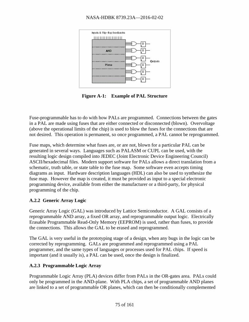
NASA-HDBK 8739.23A—2016-02-02
75 of 161
Figure A-1: Example of PAL Structure
Fuse-programmable has to do with how PALs are programmed. Connections between the gates in a PAL are made using fuses that are either connected or disconnected (blown). Overvoltage (above the operational limits of the chip) is used to blow the fuses for the connections that are not desired. This operation is permanent, so once programmed, a PAL cannot be reprogrammed.
Fuse maps, which determine what fuses are, or are not, blown for a particular PAL can be generated in several ways. Languages such as PALASM or CUPL can be used, with the resulting logic design compiled into JEDEC (Joint Electronic Device Engineering Council) ASCII/hexadecimal files. Modern support software for PALs allows a direct translation from a schematic, truth table, or state table to the fuse map. Some software even accepts timing diagrams as input. Hardware description languages (HDL) can also be used to synthesize the fuse map. However the map is created, it must be provided as input to a special electronic programming device, available from either the manufacturer or a third-party, for physical programming of the chip.
A.2.2 Generic Array Logic
Generic Array Logic (GAL) was introduced by Lattice Semiconductor. A GAL consists of a reprogrammable AND array, a fixed OR array, and reprogrammable output logic. Electrically Erasable Programmable Read-Only Memory (EEPROM) is used, rather than fuses, to provide the connections. This allows the GAL to be erased and reprogrammed.
The GAL is very useful in the prototyping stage of a design, when any bugs in the logic can be corrected by reprogramming. GALs are programmed and reprogrammed using a PAL programmer, and the same types of languages or processes used for PAL chips. If speed is important (and it usually is), a PAL can be used, once the design is finalized.
A.2.3 Programmable Logic Array
Programmable Logic Array (PLA) devices differ from PALs in the OR-gates area. PALs could only be programmed in the AND-plane. With PLA chips, a set of programmable AND planes are linked to a set of programmable OR planes, which can then be conditionally complemented

NASA-HDBK 8739.23A—2016-02-02
76 of 161
to produce an output. PLA devices allow far more design options than PALs, but the downside is reduced performance.
Like PALs, PLA devices are fuse-based and can be programmed only once. Tools and languages are readily available to translate a logic design into the fuse map required for PLA programming. Table A-1 gives a comparison of the simple programmable devices.
Table A-1: Simple PLD Comparisons
PROM PAL GAL PLA Input lines hard-wired programmable programmable programmable
Output lines programmable hard-wired programmable programmable
Versatility low moderate moderate high
Difficulty in manufacturing, programming, and testing
low moderate low high
Reprogrammable? No No Yes No
A.3 Complex Programmable Logic Devices (CPLD)
Simple PLDs can only handle up to 10 to 20 logic equations, which is not a very large logic design. Designers need to figure out how to break a larger design apart and fit the pieces into a set of PLDs. This is a time-consuming process, and means the designer has to interconnect the PLDs with wires. When there were only discrete logic chips, the use of wires meant that any design change will likely require a new circuit board, not just reprogramming the PLDs. To counteract this constraint, the chip makers began by building much larger programmable chips, including CPLDs and FPGAs.
A CPLD contains a set of PLD blocks whose inputs and outputs are connected together by a global interconnection matrix. Therefore, a CPLD has two levels of programmability; each PLD block can be programmed, and then the interconnections between the PLDs can be programmed. A key feature of the CPLD architecture is the arrangement of logic cells on the periphery of a central shared routing resource. CPLDs use EEPROM, SRAM, or Flash memory to hold the interconnect information.
CPLDs contain the equivalent of many PALs linked by programmable interconnections, all in one integrated circuit. CPLDs are equivalent to about 50 typical PLD devices and can replace thousands, or even hundreds of thousands, of logic gates.
Programming CPLDs depends on the chip and the application. Some CPLDs can be programmed in a PAL programmer, but that gets difficult if the chip has hundreds of pins, or is surface-mounted. Many CPLDs can be programmed over a serial line from a computer. The CPLD contains a circuit that decodes the data stream and configures the CPLD to perform its specified logic function.

NASA-HDBK 8739.23A—2016-02-02
77 of 161
An interface for programming and testing CPLDs is Joint Test Action Group (JTAG). This interface is defined by the IEEE Standard 1149.1-1990, Test Access Port and Boundary Scan Architecture. Boundary scan is a technique for accessing and stimulating a chip or subsystem via external pins to perform internal test functions on the device. A JTAG interface is primarily used for testing integrated circuits, but it can also be used as a mechanism for debugging embedded systems. A JTAG interface is a special four-pin (data in, data out, clock, test mode select) interface added to a chip. Multiple chips on a board can have their JTAG lines daisy-chained together, so the test probe only needs to connect to a single JTAG port to have access to all chips on a circuit board. Figure A-2 shows the difference between the internal layouts of a CPLD vs. FPGA device.

NASA-HDBK 8739.23A—2016-02-02
78 of 161
CPLD Diagram FPGA Diagram
Figure A-2: CPLD vs. FPGA Layout
A.4 Field Programmable Gate Array (FPGA)
While PALs were busy developing into GALs and CPLDs, a separate stream of development was occurring, based on gate-array technology. The resulting device is the FPGA which was first introduced in the late 1970s. “Field programmable” simply means the device can be programmed by the user. Many field programmable devices can be programmed with the chip soldered to the circuit board, allowing true in-the-field upgrades to be possible.
FPGAs use a grid of logic gates, similar to that of an ordinary gate array. An FPGA has a collection of simple, configurable logic blocks arranged in an array with interspersed switches that can rearrange the interconnections between the logic blocks. Each logic block is individually programmed to perform a logic function (such as AND, OR, XOR, etc.) and then the switches are programmed to connect the blocks so the complete logic functions are implemented. FPGAs vary in size from tens of thousands of logic gates to over one million.
The interconnections for the logic blocks are programmable switches. FPGAs may use EEPROM, SRAM, antifuse, or Flash technology to store the programming. In manylarger FPGAs the configuration is volatile, and must be re-loaded into the device whenever power is applied or different functionality is required.
FPGAs are typically programmed in hardware description languages (HDLs) like Verilog or VHDL. These high-level languages are used because manual lower level design (such as schematic capture) becomes impractical as designs become large. HDLs also allow the FPGA design to be simulated and tested prior to implementation in the hardware.

NASA-HDBK 8739.23A—2016-02-02
79 of 161
A.5 Application Specific Integrated Circuit (ASIC)
ASICs are integrated circuits (ICs) designed for specific applications. Unlike standard ICs which are produced by the chip manufacturers, ASICs are designed by the end user and then produced in volume. ASICs allow a user to combine many parts and functions into a single chip, reducing cost and improving reliability.
ASICs can be large or small. They are usually produced in large quantities, and it can be very expensive to produce only a few. If manufacturing cell phones, it makes sense to develop an ASIC for the device. If flying a space experiment and need at most a few chips, it would be much more economical to use programmable logic, such as FPGA or CPLD devices.
An interesting twist is the production of ASICs that include programmable logic (FPGA, CPLD or PAL) devices as part of the chip. Another new technology that combines ASICs with programmable parts is the System-on-Chip, described below.
A.6 System-on-Chip (SoC)
System-on-Chip combines all the electronics for a complete product into a single chip. SoCs include not only the brains (e.g., microprocessor) but also all required ancillary electronics, such as switches, comparators, resistors, capacitors, timing elements, and digital logic. Figure A-3 gives a sample configuration for a SoC.
SoCs could include:
Digital/analog functions
Sensors
I/O
Communications
Readymade sub-circuits (IP)
Programmable devices
Digital Signal Processor
Figure A-3: SoC Example Configuration
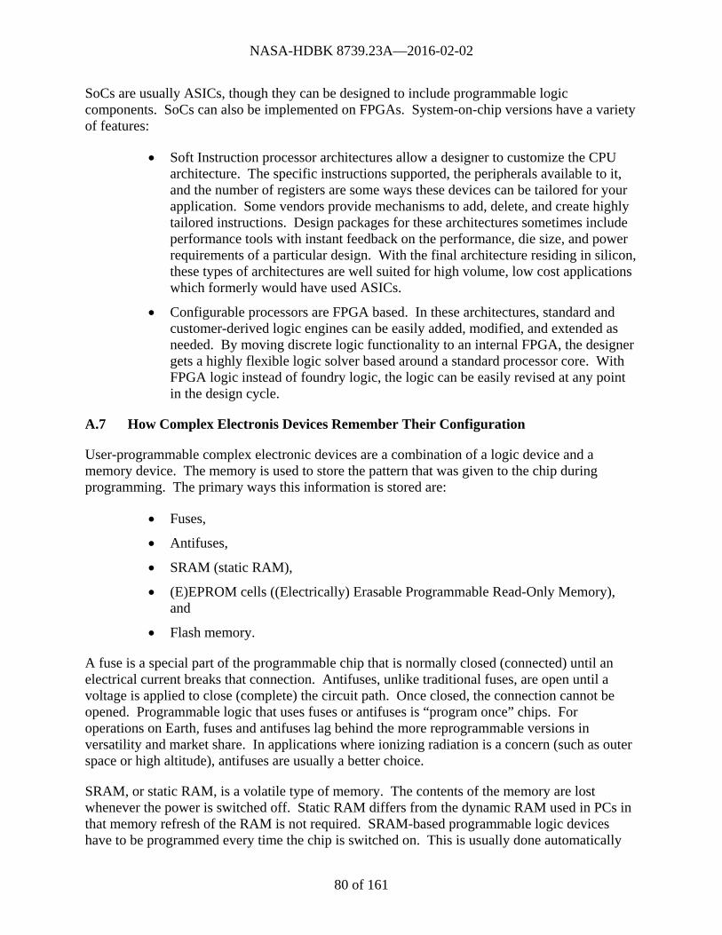
NASA-HDBK 8739.23A—2016-02-02
80 of 161
SoCs are usually ASICs, though they can be designed to include programmable logic components. SoCs can also be implemented on FPGAs. System-on-chip versions have a variety of features:
Soft Instruction processor architectures allow a designer to customize the CPU architecture. The specific instructions supported, the peripherals available to it, and the number of registers are some ways these devices can be tailored for your application. Some vendors provide mechanisms to add, delete, and create highly tailored instructions. Design packages for these architectures sometimes include performance tools with instant feedback on the performance, die size, and power requirements of a particular design. With the final architecture residing in silicon, these types of architectures are well suited for high volume, low cost applications which formerly would have used ASICs.
Configurable processors are FPGA based. In these architectures, standard and customer-derived logic engines can be easily added, modified, and extended as needed. By moving discrete logic functionality to an internal FPGA, the designer gets a highly flexible logic solver based around a standard processor core. With FPGA logic instead of foundry logic, the logic can be easily revised at any point in the design cycle.
A.7 How Complex Electronis Devices Remember Their Configuration
User-programmable complex electronic devices are a combination of a logic device and a memory device. The memory is used to store the pattern that was given to the chip during programming. The primary ways this information is stored are:
Fuses,
Antifuses,
SRAM (static RAM),
(E)EPROM cells ((Electrically) Erasable Programmable Read-Only Memory), and
Flash memory.
A fuse is a special part of the programmable chip that is normally closed (connected) until an electrical current breaks that connection. Antifuses, unlike traditional fuses, are open until a voltage is applied to close (complete) the circuit path. Once closed, the connection cannot be opened. Programmable logic that uses fuses or antifuses is “program once” chips. For operations on Earth, fuses and antifuses lag behind the more reprogrammable versions in versatility and market share. In applications where ionizing radiation is a concern (such as outer space or high altitude), antifuses are usually a better choice.
SRAM, or static RAM, is a volatile type of memory. The contents of the memory are lost whenever the power is switched off. Static RAM differs from the dynamic RAM used in PCs in that memory refresh of the RAM is not required. SRAM-based programmable logic devices have to be programmed every time the chip is switched on. This is usually done automatically

NASA-HDBK 8739.23A—2016-02-02
81 of 161
by another part of the system. SRAM FPGAs are susceptible to ionizing radiation, including the neutron radiation experienced at high altitudes.
An EPROM cell is a transistor that can be switched on by trapping an electric charge permanently on its gate electrode. This is done by an external programming device. The charge remains for many years and can only be removed by exposing the chip to strong ultraviolet light. EEPROM is electrically erasable PROM, which uses an electrical current rather than ultraviolet light to erase the programmed value. EPROMs have to be removed from their circuit boards to be erased and reprogrammed. EEPROMs can be erased and reprogrammed using special circuitry on the board.
Flash memory is non-volatile, which means it retains its contents even when the power is switched off. It can be erased and reprogrammed as required. This makes it useful for programmable logic device memory. Flash-based devices combine the best of both worlds - maintaining configuration when not powered, but also allowing reprogramming when desired. Flash-based programmable devices are essentially immune to neutron radiation (generated when cosmic rays interact with the atmosphere) and are resistant to other high-energy particles.
A.7.1 Externally Programmed Devices
Complex electronics using fuse, antifuse, or EPROM technology to configure the device have to be programmed in an external device, and cannot be programmed when placed on a circuit board. EEPROM-based devices may also require external programming, or may be able to be programmed in-system, depending on the specifics of the device and the circuit.
To use an external programmer the chip (CPLD or FPGA, or simple programmable logic device) is placed in the appropriate socket and attached to the programming device (see Figure A-4). The programmer is attached to a computer (or may have an internal microprocessor, for stand-alone devices), which will download the binary file into the device and then apply the necessary voltages to “burn” or program the chip.
Figure A-4: External Programmer
A.7.2 In-system Programming
Complex electronics using SRAM, Flash, or (sometimes) EEPROM can be, and usually are, programmed in-situ on the circuit board. Many boards provide a JTAG interface that can be hooked up to a personal computer for download of the device configuration.

NASA-HDBK 8739.23A—2016-02-02
82 of 161
A.7.3 ASICs
Application Specific Integrated Circuits are user-designable, not user-programmable complex electronics. While the basic steps in designing ASICs are the same as for other complex electronics, there are some differences, driven by the fact that ASICs are manufactured (usually in large runs), and a problem with the resulting chip is very costly.
Table A-2 lists some of the main differences between creating an ASIC and a programmable complex electronic device (e.g., FPGA).
Table A-2: FPGA vs. ASIC Comparison
Development Area Differences
Vendor Selection With FPGAs, you select which chip to use. This is an off-the-shelf purchase, and the only question is whether the chip meets design needs and how good the vendor-supplied tools are. Since ASICs are manufactured, the vendor relationship is much more important. ASIC vendors will usually perform some of the implementation steps (such as place and route), as well as post-manufacture testing.
Careful Selection of Functionality
Because failure cost of ASIC designs is high, the selection of what functionality will be included in the ASIC is very important. While FPGA design, like software, can be changed later in the program, ASICs have a long lead time. So it is important to get everything right early in the process.
Simulation With FPGA designs, the primary simulations to verify design functionality are early in the design process. With ASICs, simulations are mostly performed late in the design (at the gate level) to verify that all the last minute transformations and modifications do not cause an error. This difference affects what is wanted in a simulation environment. For ASICs, high performance (fast) simulation is essential. For FPGAs, the quality of the user environment and the speed in locating and fixing errors is more important.
Design Size The size (in gates and/or I/O capacity) of ASICs is a somewhat continuous scale from small to very large. FPGAs are “chunky” - the size varies in vendor-defined increments within a device family. ASICs have more flexibility in size, so that a small increase will not affect the final cost too much. With an FPGA it might be necessary to go to the next higher size chip (i.e. more expensive chip). In general, FPGA designers are more concerned with getting the design to the minimum size (or to fit within the target chip) than ASIC designers.
Timing ASICs have a relatively smooth, continuous distribution of delays as routing distances vary. With FPGAs, delays move in large, discontinuous, and relatively unpredictable steps. This means the estimated timing performance can vary by 20-30% on a net-by-net and path-by-path basis between the various design tools. With ASICs, many timing problems can often be conquered by resizing buffers, small placement and routing changes, and cell swaps. These options are not available with FPGAs. Logic synthesis in FPGA can basically only replicate logic, rebalance trees, and restructure paths to resolve timing issues.

NASA-HDBK 8739.23A—2016-02-02
83 of 161
Development Area Differences
Verification In the ASIC world, verification is a long and time consuming process. It will take up to 70% of the total development time and resources. The reason for this is risk avoidance - a design error can cause the project to waste all the time and money spent on the ASIC. This makes verification, confirmation, and re-verification every design engineer’s first priority. Verification of ASICs is a lot more rigorous than FPGA verification. Besides multiple simulations at various design phases, and design reviews with your best engineers, two additional verification activities may be performed: Prototyping in FPGA. Creating your ASIC design in an FPGA prototype results in discovery of bugs that may not have been identified during previous simulations. It also provides multiple platforms for software development in parallel to debugging. The FPGA prototype is available for the post-manufacture verification as an exerciser to validate the design. Formal Methods. Formal methods in the engineering world are those methods using mathematical (formal) languages for writing specifications to prove highest-level specifications are consistent with top-level objectives. They have an advantage over verbal prose and conventional simulators because they can be used to represent specifications that are provably consistent with objectives and higher level specifications.
Manufacturing Programmable complex electronics use off-the-shelf chips, whereas an ASIC design is submitted to a vendor for manufacturing. The manufacturing stage incurs significant expense. The vendor assumes responsibility for fabricating, probing, and sorting wafers then assembles and packages the chip per requirements. Once the chips are created (and pass the vendor tests), the designer has to complete verification of the final product - and hope the design was correct. Any problems found will require the ASICs to be remanufactured, at a significant cost.
A.7.4 SRAM-based FPGAs
Complex electronics using SRAM will lose their memory once power is removed. Static RAM is volatile memory, thus SRAM chips need additional resources in order to function. Since the configuration is lost whenever the power is removed, the FPGA configuration has to be placed in non-volatile memory, such as an EPROM, EEPROM, or Flash memory. When the FPGA is powered on, it reads the configuration from the non-volatile memory and is ready to go.

NASA-HDBK 8739.23A—2016-02-02
84 of 161
APPENDIX B HARDWARE DESCRIPTION LANGUAGES
B.1 Overview of Hardware Description Languages (HDLs)
While schematic capture works well for small circuits and devices, complex designs require the ability to abstract at a higher level. Thus, hardware description languages were born. One difference between HDLs and software languages is HDLs are essentially models of the hardware. The languages were initially created to allow simulation of the design and contain all the necessary capabilities to create test benches and simulation models. Simulation of complex electronics is very common in the design community.
There are two major HDLs currently in use: Verilog and VHDL. This handbook provides a cursory overview of these two languages; however, each of the languages is a course (or two) in its own right. Several good tutorials on the languages are provided in Section 2.2, Links.
The Verilog hardware description language was invented by Philip Moorby in 1983.The first Verilog synthesis tool was introduced in 1987. Verilog was placed in the public domain and is now specified by an IEEE standard (IEEE 1364). This language enables specification of a digital system at a range of levels of abstraction, such as switches, gates, Register-Transfer Level (RTL), and higher. In 2005, SystemVerilog was adopted as IEEE Standard 1800-2005. This update includes items such as structures, pointers, or recursive subroutines not present in earlier versions.
VHDL stands for VHSIC Hardware Description Language. VHSIC is an acronym for Very High Speed Integrated Circuit. VHDL is also specified by an IEEE standard (IEEE 1076). VHDL was developed over time, culminating in its initial release in 1987. In June 2006, the VHDL Technical Committee of Accellera approved Draft 3.0 of VHDL-2006. While maintaining full compatibility with older versions, this proposed standard provides numerous extensions that make writing and managing VHDL code easier. Key changes include incorporation of child standards (1164, 1076.2, 1076.3) into the main 1076 standard, an extended set of operators, more flexible syntax of 'case' and 'generate' statements, incorporation of VHPI (interface to C/C++ languages), and a subset of PSL (Property Specification Language).
B.2 General Hardware Description Language Concepts
There are a few major differences between HDLs and software languages that one needs to keep in mind. First, software is inherently sequential - one instruction is executed after another. Even in multi-threaded or multi-tasking systems, no two tasks operate at the exact same moment. Hardware, however, is parallel in nature - multiple events can be happening simultaneously. Hardware description languages have ways to describe concurrency (parallel execution) and to specify timing. Second, HDLs describe hardware. While at the highest abstraction an HDL can define an algorithm similarly to a software language, at the lower levels of abstraction that algorithm is translated into gates and I/O.
Hardware description languages model two aspects of the hardware: structure and behavior. These two aspects are independent - the structure of the hardware is not dependent on the behavior, and vice versa. The interfaces (input/output signals) from the device to the outside

NASA-HDBK 8739.23A—2016-02-02
85 of 161
world are part of both the structure (what the device is made of) and the behavior (what it does with the signals). In addition, because HDLs were originally designed as simulation languages, they can create test benches to exercise and test the device with simulated “real world” devices.
The first step when designing and modeling complex electronics in a hardware description language is to partition the design into natural abstract blocks, known as components. Each component is the instantiation of a design entity, which is normally modeled in a separate system file for easy management and individual compilation by simulation or synthesis tools. The total system is then modeled using a hierarchy of components, known as a design hierarchy, which consists of individual subcomponents (subdesign entities) brought together in one higher-level component (design entity). In other words, start with very simple entities (e.g., AND gates) and put them together into components (logical subdivisions within the device), which together become the model of the device.
The two main elements of the HDL description of the complex electronic device are the architecture body (the structure) and the behavioral architecture. The architecture body describes the implementation of a module’s inputs and/or outputs. The electrical values of the outputs are some function of the values of the inputs. Of course, each module can be made up of sub-modules, down to the basic entities. The connections between the sub-modules (inputs/outputs) are made using signals.
The architecture body contains:
Signal declarations, for internal interconnections,
Entity ports (also treated as signals),
Component instances (instances of previously declared entity/architecture pairs),
Port maps in component instances (connect signals to component ports), and
Wait statements.
The behavioral architecture describes the algorithm performed by the module. While the architecture body described the inputs and outputs, the behavioral architecture describes what goes on to convert those inputs to outputs. More complex behaviors cannot be described purely as a function of inputs. In systems with feedback, the outputs are also a function of time. Fortunately, hardware description languages provide features to handle time as part of the behavior.
The behavioral architecture contains:
Process statements,
Sequential statements,
Signal assignment statements, and
Wait statements.

NASA-HDBK 8739.23A—2016-02-02
86 of 161
The design engineer can describe the behavior of a module without describing its structure. This might want to be doneif using an off-the-shelf component as part of the design. The design engineer does not really care about the internal structure of the component; they just want to describe what it does. Figure B-1 shows the general HDL development process.

NASA-HDBK 8739.23A—2016-02-02
87 of 161
Figure B-1: General HDL Development
NASA-HDBK 8739.23A—2016-02-02
88 of 161
This handbook does not provide significant detail on the two main hardware description languages (VHDL and Verilog). See the links below for some tutorials on VDHL or Verilog.
B.2.1 VHDL Tutorials
http://www.seas.upenn.edu/~ese201/vhdl/vhdl_primer.html
http://www.gmvhdl.com/VHDL.html
B.2.2 Verilog Tutorials
http://www.asic-world.com/verilog
http://www.doulos.com/knowhow/verilog_designers_guide/
B.2.3 Comparison of VHDL and Verilog
The design engineer can design complex electronics in either of the main hardware description languages (VHDL and Verilog). Both provide all the capabilities required. While the choice of language is mostly a personal preference, there are some differences between the two that may be important for specific applications. Table B-1 shows how the two compare.
Table B-1: VHDL vs. Verilog
VHDL Verilog
Similarity to software
programming language
Pascal and Ada C
Level of abstraction
VHDL models well from the system level down to the RTL level, with some modeling at the gate level.
Verilog has less system modeling capabilities than VHDL, but more capabilities at the gate level.
Compilation Allows separate compilation of multiple design-units (entity/architecture pairs) that reside in the same system file.
With Verilog, care must be taken with both the compilation order of code written in a single file and the compilation order of multiple files. Simulation results can change by simply changing the order of compilation.

NASA-HDBK 8739.23A—2016-02-02
89 of 161
VHDL Verilog
Data types
VHDL has a multitude of language or user defined data types. As a result, dedicated conversion functions are needed to convert objects from one type to another.
Verilog data types are very simple, easy to use and very much geared towards modeling hardware structure as opposed to abstract hardware modeling. All data types used in a Verilog model are defined by the Verilog language and not by the user.
Design reusability Procedures and functions may be placed in a package so that they are available to any design-unit needing them.
There is no concept of packages in Verilog. Functions and procedures used within a model must be defined in the module.
Ease of learning
VHDL may seem less intuitive at first for two primary reasons. First, it is very strongly typed; a feature making it robust and powerful for the advanced user after a longer learning phase. Second, there are many ways to model the same circuit, especially those with large hierarchical structures.
Probably easiest to learn with no prior exposure or knowledge.
High level constructs
VHDL contains more constructs and features for high-level modeling than Verilog. Abstract data types can be used along with the following statements: package statements for model reuse configuration statements for configuring design structure generate statements for replicating structure generic statements for generic models that can be individually characterized
Verilog has no high-level modeling statements similar to VHDLs. Verilog allows parameterized models by overloading parameter constants.
Language extensions
VHDL allows architectures and subprograms to be modeled in another language by using the “foreign” attribute.
The Programming Language Interface (PLI) is an interface mechanism between Verilog models and Verilog software tools.
Libraries
VHDL uses a library to store compiled entities, architectures, packages and configurations. Useful for managing multiple design projects
There is no concept of a library in Verilog. This is due to its origins as an interpretive language.
Low level constructs
Simple two input logical operators are built into the language, they are: NOT, AND, OR, NAND, NOR, XOR and XNOR. Any timing must be separately specified.
The Verilog language was originally developed with gate level modeling in mind and has very good constructs for modeling at this level and for modeling the cell primitives of ASIC and FPGA libraries.
Managing large designs
Configuration, generate, generic, and package statements all help manage large design structures.
There are no statements in Verilog that help manage large designs.
Operators Similar operators to Verilog with the addition of a mod operator.
Similar operators to VHDL with the addition of a unary reduction operator.

NASA-HDBK 8739.23A—2016-02-02
90 of 161
VHDL Verilog
Parameterizable models
A specific bit width model can be instantiated from a generic n-bit model using the generic statement.
A specific bit model can be instantiated from a generic n-bit model using overloaded parameter values.
Procedures and tasks
Allows concurrent procedure calls. Does not allow concurrent task calls.
Readability (This is more a
matter of coding style and
experience than language feature)
VHDL is a verbose language; its roots are based on Ada.
Verilog is more like C because its constructs are based approximately 50% on C and 50% on Ada.
Structural replication
The generate statement replicates a number of instances of the same design-unit or some subpart of a design and connects it appropriately.
There is no equivalent to the generate statement in Verilog.
Test harnesses VHDL has generic and configuration statements useful in test harnesses.
Verilog does not have similar statements.
Verboseness
Because VHDL is a very strongly typed language, models must be coded precisely with defined and matching data types. Models are often more verbose, and the code often longer, than its Verilog equivalent.
Verilog allows signals representing objects of different bit-widths to be assigned to each other. The signal representing the smaller number of bits is automatically padded out to that of the larger number of bits. This has the advantage of not needing to model quite as explicitly as in VHDL, but does mean unintended modeling errors will not be identified by an analyzer.
B.2.4 Coding Standards
Just as in writing software for embedded applications, a coding standard is important whenever more than one person will have to maintain the source code. The big danger is that when the person who wrote the original code leaves or moves on to another project, no one will understand how it works if the code ever has to change. Even the original designer is likely to forget it in several months.
One can easily write individual lines of understandable HDL code that collectively become extremely difficult to follow. A good coding standard will help alleviate this by providing guidelines for hierarchical structures and component instantiations. For instance, many books use various types of flip-flops as examples to model component instantiations (mostly because these are already understood by the readers). However, in practice, it is generally poor coding style to instantiate logic by mapping each register to various kinds of flip-flops. This can lead to longer, more obfuscating logic that does not take advantage of the ability to write in VHDL and Verilog at a higher level.
Some important elements of an HDL coding standard are:

NASA-HDBK 8739.23A—2016-02-02
91 of 161
Consistent and defined style,
Guidelines on writing understandable code,
Commenting guidelines,
Information to capture in comments at each level, and
Naming convention (for consistency).
Coding standards can be specific to a programming language or a chip family, or corporate requirements, or more general in nature. An example coding standard, courtesy of Xilinx Corporation, can be found in Appendix D.
B.3 Programming ExampleS
The following examples demonstrate, in a simple form, the programming constructs for complex electronics.
VHDL uses the concept of a “design entity,” which consists of two design units. The entity declaration defines the external interface. The architecture body details the internal structure, and can define the entity’s behavior, structure, or both.
Verilog uses the concept of a “module” rather than “entity.” Like VHDL, the port declarations (external interface) are separate from the module body, which defines the internal behavior and/or structure. Figure B-2 below, which includes Examples 1 and 2, shows the difference between a VHDL and Verilog design for the same circuit.
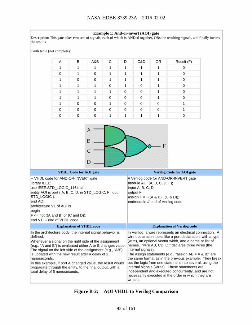
NASA-HDBK 8739.23A—2016-02-02
92 of 161
Example 1: And-or-invert (AOI) gate Description: This gate takes two sets of signals, each of which is ANDed together, ORs the resulting signals, and finally inverts the results.
Truth table (not complete):
A B A&B C D C&D OR Result (F)
1 1 1 1 1 1 1 0
0 1 0 1 1 1 1 0
1 0 0 1 1 1 1 0
1 1 1 0 1 0 1 0
1 1 1 1 0 0 1 0
1 1 1 0 0 0 1 0
1 0 0 1 0 0 0 1
0 0 0 0 0 0 0 1
0 0 0 1 1 1 1 0
VDHL Code for AOI gate Verilog Code for AOI gate
-- VHDL code for AND-OR-INVERT gate library IEEE; use IEEE.STD_LOGIC_1164.all; entity AOI is port ( A, B, C, D: in STD_LOGIC; F : out STD_LOGIC ); end AOI; architecture V1 of AOI is begin F <= not ((A and B) or (C and D)); end V1; -- end of VHDL code
// Verilog code for AND-OR-INVERT gate module AOI (A, B, C, D, F); input A, B, C, D; output F; assign F = ~((A & B) | (C & D)); endmodule // end of Verilog code
Explanation of VHDL code Explanation of Verilog code
In the architecture body, the internal signal behavior is defined. Whenever a signal on the right side of the assignment (e.g., “A and B”) is evaluated either A or B changes value. The signal on the left side of the assignment (e.g., “AB”) is updated with the new result after a delay of 2 nanoseconds. In this example, if port A changed value, the result would propagate through the entity, to the final output, with a total delay of 5 nanoseconds.
In Verilog, a wire represents an electrical connection. A wire declaration looks like a port declaration, with a type (wire), an optional vector width, and a name or list of names. “wire AB, CD, O;” declares three wires (the internal signals). The assign statements (e.g., “assign AB = A & B;” are the same format as in the previous example. They break out the logic from one statement into several, using the internal signals (wires). These statements are independent and executed concurrently, and are not necessarily executed in the order in which they are written.
Figure B-2: AOI VHDL to Verilog Comparison

NASA-HDBK 8739.23A—2016-02-02
93 of 161
B.4 Abstraction
Hardware description languages can be used to describe complex electronics at many different levels of abstraction. An abstraction is a simplified representation of something that is potentially quite complex. It is often not necessary to know the exact details of how something works, is represented or is implemented, because it can be used in its simplified form.
The levels of abstraction for a complex electronic device are:
System or Behavioral,
Algorithm,
Register-Transfer Level (RTL), and
Gate.
The highest level of abstraction is the system level, where the device is mostly a black box interacting with its environment. Very little is known about the internals of the device, but it functions (its behavior) are defined.
A pure algorithm consists of a set of instructions executed in sequence to perform some task. A pure algorithm has neither a clock nor detailed delays. Some aspects of timing can be inferred from the partial ordering of operations within the algorithm. The algorithmic level of abstraction is similar to software programming (e.g.; while ready, do task A and task B, then do task C). Because of the lack of timing information, this level is not synthesizable (able to be mapped to hardware).
The Register-Transfer Level (RTL) description has an explicit clock. All operations are scheduled to occur in specific clock cycles, but there are no detailed delays below the cycle level. A single global clock is not required but may be preferred. In addition, re-timing is a feature allowing operations to be rescheduled across clock cycles. The RTL level is the input to the synthesis tool.
The gate level of abstraction is the output from the synthesis tool. A gate level description consists of a network of gates and registers, along with technology-specific delay information for each gate. A complex electronics device can be described in one of three domains: behavioral, structural, and physical. Figure B-3 shows the various domains in which complex electronics can be described.

NASA-HDBK 8739.23A—2016-02-02
94 of 161
Figure B-3: Complex Electronics Domains
Hardware description languages deal with the first two domains (behavioral and structural). The mapping from the behavioral and structural domains to the physical implementation is performed by the synthesis and place-and-route tools.
Figure B-4 shows a simple circuit that warns car passengers when the door is open or the seatbelt is not used whenever the car key is inserted in the ignition lock. At the behavioral level this could be expressed as:
Warning = Ignition_on AND (Door_open OR Seatbelt_off)
Figure B-4: Warning Buzzer Example
The structural level, on the other hand, describes a system as a collection of gates and components interconnected to perform a desired function. A structural description could be compared to a schematic of interconnected logic gates. It is a representation usually closer to the physical realization of a system.

NASA-HDBK 8739.23A—2016-02-02
95 of 161

NASA-HDBK 8739.23A—2016-02-02
96 of 161
APPENDIX C EXAMPLES
C.1 CPLD
Device name: Complex Programmable Logic Device (CPLD)
Figure C-1: CPLD
Description:
A CPLD, Figure C-1, contains a set of simpler Programmable Logic Device (PLD) blocks whose inputs and outputs are connected together by a global interconnection matrix. Therefore, a CPLD has two levels of programmability: each PLD block can be programmed, and then the interconnections between the PLDs can be programmed. A key feature of the CPLD architecture is the arrangement of logic cells on the periphery of a central shared routing resource. CPLDs are equivalent to about 50 typical PLD devices, and can replace thousands, or even hundreds of thousands, of logic gates.
Programming and Reprogramming
CPLDs vary in how they can be programmed or reprogrammed, depending on their underlying structure. The three basic types of CPLDs are:
Fuse or antifuse. These CPLDs are programmed by passing a large current through the connections (fuses). The current “blows” the fuse to break a connection. The CPLDs are one-time programmable because once the fuses are blown they cannot be rewired internally. Programming occurs in a special device external to the circuit board the CPLD will be placed on.
EPROM or EEPROM. In these CPLDs, the interconnections are made by opening and closing transistors by storing a charge on their gate electrodes using a high-voltage pulse. For EPROM-like CPLDs, erasing the CPLD is done by placing it in a special programmer socket and reprogramming it. Reprogramming is not possible once the chip is soldered to its circuit board. EEPROM-like

NASA-HDBK 8739.23A—2016-02-02
97 of 161
CPLDs may be reprogrammable on the circuit board, if special circuitry is included.
SRAM or Flash. Static RAM (SRAM) or Flash memory can be used to control the transistors for each interconnection. Each memory bit controls the interconnect switches through its value. When a bit is set to ‘1,’ the switch is closed, and the logic elements are connected. A ‘0’ opens the switch. CPLDs built using RAM/Flash switches can be reprogrammed without removing them from the circuit board and are in-circuit reconfigurable or in-circuit programmable.
There are tools which determine what switches to open or close to implement the logic design. These tools take the logic design and output a binary file which configures the switches in a CPLD.
Applications:
CPLDs are used in a wide variety of applications from cell phones to spacecraft. They are often used as “glue logic” to connect various parts of a design, process data, or to translate data from one protocol to another. CPLDs are great for:
High speed operations,
Interface controllers (bus, memory, Flash),
Interface bridging,
I/O expansion,
Device configuration,
Power-up sequencing,
Microprocessor support logic,
Glue logic, and
Implementing small “soft” microcontrollers (e.g., 8-bit).
They are used as support chips in most modern electronics, including:
Cell phones,
PDAs,
Digital cameras,
Communications hardware, and
GPS.
CPLDs come in a variety of density, speed, and package options. Handheld applications tend to use lower density devices, because they have less need for complex logic, require low power,

NASA-HDBK 8739.23A—2016-02-02
98 of 161
and try to minimize cost per unit. When capability is more important than power usage, higher density CPLDs are a better choice.
Often a logic design could be implemented in either a CPLD or an FPGA. CPLDs are chosen when predictable timing performance is required. CPLDs have fewer routing matrices than FPGAs. Since each routing matrix adds a little delay to the signal, fewer routings translates to faster signal transit. While CPLD density is less than most FPGAs, high end CPLDs will have the same density as low end FPGAs. Performance of CPLDs is usually better than FPGAs, though it depends on the vendor, size (number of cells), speed, and other factors.
Real-world Examples:
Here are some examples of CPLDs used in a variety of products.

NASA-HDBK 8739.23A—2016-02-02
99 of 161
MicroDosimeter Instrument (MIDN)
Figure C-2: MIDN
MIDN, Figure C-2, was a spaceflight payload that tested a compact, low powered, and portable solid-state micro dosimeter. MIDN collected quantitative information on the dose and dose distribution of energy deposited in tissue-sized silicon cells. By inference, this data could show what the dosage would be in living tissue.
CPLDs were used in MIDN for command and data handling. This payload was part of the MidSTAR-1 (Midshipman Space Technology Applications Research) satellite which operated from 2007-2009.
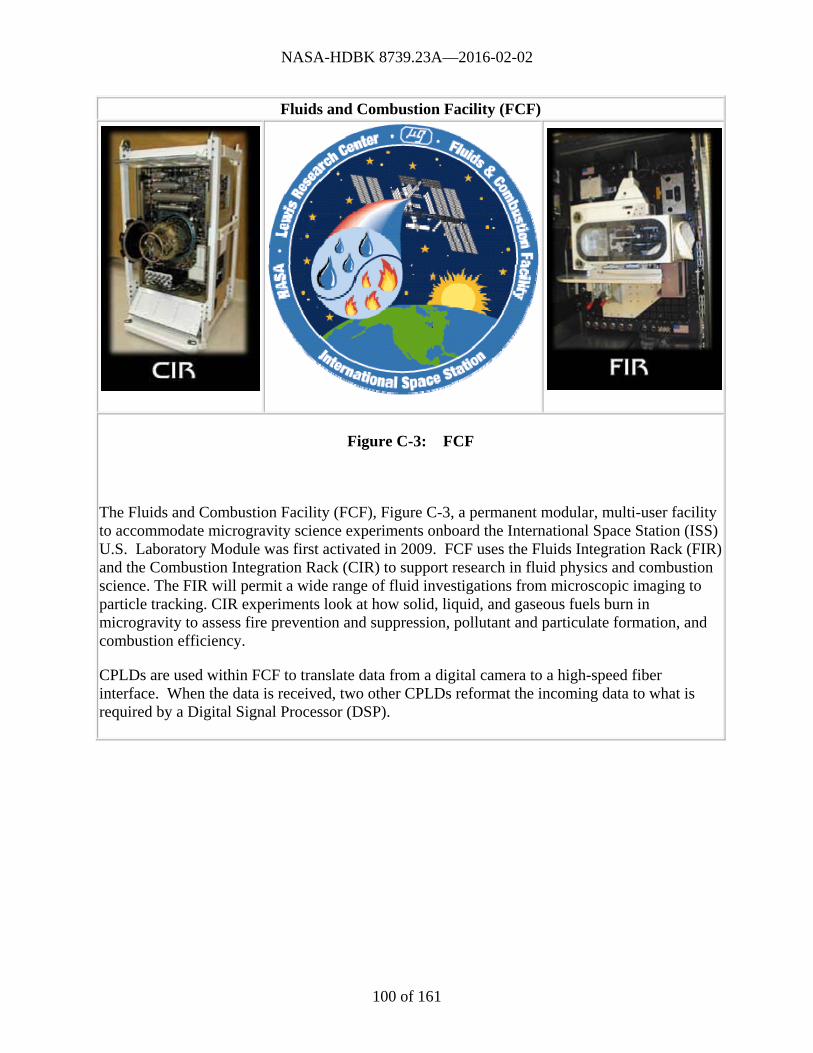
NASA-HDBK 8739.23A—2016-02-02
100 of 161
Fluids and Combustion Facility (FCF)
Figure C-3: FCF
The Fluids and Combustion Facility (FCF), Figure C-3, a permanent modular, multi-user facility to accommodate microgravity science experiments onboard the International Space Station (ISS) U.S. Laboratory Module was first activated in 2009. FCF uses the Fluids Integration Rack (FIR) and the Combustion Integration Rack (CIR) to support research in fluid physics and combustion science. The FIR will permit a wide range of fluid investigations from microscopic imaging to particle tracking. CIR experiments look at how solid, liquid, and gaseous fuels burn in microgravity to assess fire prevention and suppression, pollutant and particulate formation, and combustion efficiency.
CPLDs are used within FCF to translate data from a digital camera to a high-speed fiber interface. When the data is received, two other CPLDs reformat the incoming data to what is required by a Digital Signal Processor (DSP).

NASA-HDBK 8739.23A—2016-02-02
101 of 161
C.2 FPGA
Device name: Field Programmable Gate Array (FPGA)
Figure C-4: FGPA
Description:
A FPGA, shown in Figure C-4, is a collection of simple, configurable logic blocks arranged in an array with interspersed switches that can rearrange the interconnections between the logic blocks. Each logic block is individually programmed to perform a logic function (such as AND, OR, XOR, etc.) and then the switches are programmed to connect the blocks so that the complete logic functions are implemented.
The interconnections for the logic blocks are programmable switches. FPGAs may use EEPROM, SRAM, antifuse, or Flash technology to store the programming. In most larger FPGAs, the configuration is volatile and must be re-loaded into the device whenever power is applied or different functionality is required.
Initially, FPGAs had only local and global routing resources (i.e., a logic block could only connect to adjacent logic blocks or to global networks). Newer FPGAs have multilevel routing hierarchies, so logic blocks can connect to different levels. Fortunately, the design software takes care of these complex issues.
Newer FPGAs are being developed that contain fixed functionality, as well as traditional programmable logic. FPGAs may contain a FIFO, arithmetic functions, memory, chip-to-chip transceivers, digital signal processor (DSP), or even an entire bus interface or microprocessor core. FPGAs with fixed functionality are cousins to the SoC devices that included programmable logic as part of their design.
NASA-HDBK 8739.23A—2016-02-02
102 of 161
SRAM FPGAs
SRAM, or static RAM, is a volatile type of memory. The contents of the memory are lost whenever the power is switched off. Static RAM differs from the dynamic RAM used in PCs in that memory refresh of the RAM is not required. SRAM-based programmable logic devices, such as FPGAs, have to be programmed every time the chip is switched on. This is usually done automatically by another part of the system.
Most SRAM-based FPGAs use a master mode, which reads the configuration information from non-volatile memory, such as a serial or parallel EPROM or flash memory. The FPGAs can also be configured via an external source in slave mode. The FPGA accepts a serial or parallel data stream representing the configuration data. The data source can be a processor, computer, or an FPGA acting as a master. Using this technique, it is possible for several FPGAs to be programmed from a single memory. A master FPGA is wired to a daisy chain of slave FPGAs. When the master FPGA has been programmed, it will keep reading the data from the memory and pass it on to the slave devices until all of the FPGAs are configured.
Antifuse FPGAs
A fuse is a special part of the programmable chip that is normally closed (connected) until an electrical current breaks the connection. Antifuses, unlike traditional fuses, are open until a voltage is applied to close (complete) the circuit path. Once programmed closed, the connection cannot be reprogrammed to open. Programmable logic using fuses or antifuses are “program once” chips.
Antifuse FPGAs are best used when you do not want to have to reconfigure your chip every time power is applied (e.g., quick power-on time is needed). They are also useful in environments where SRAM would have problems (e.g., high altitude or outer space).
Flash FPGAs
Flash memory is non-volatile, which means it retains its contents even when the power is switched off. It can be erased and reprogrammed as required. This makes it useful for programmable logic device memory. Flash-based devices combine the best of both worlds - maintaining configuration when not powered, but also allowing reprogramming when desired. Flash-based programmable devices are essentially immune to neutron radiation (generated when cosmic rays interact with the atmosphere) and are resistant to other high-energy particles.
Software Engineers and FPGAs
What if a software engineer could create a regular software application that could run on an FPGA? Design tools for FPGAs are moving quickly in this direction. In this new environment for software developers, the FPGA can be viewed as one possible target (along with traditional and non-traditional processor architectures) for a software compiler. With currently available tools, the software engineer can make use of FPGA platforms, as well as take advantage of the high level of algorithmic parallelism available when traditional processors (or processor cores) and FPGAs are combined in a single target platform.

NASA-HDBK 8739.23A—2016-02-02
103 of 161
FPGA-based computing platforms, particularly those with embedded “soft” microprocessors, have the potential to implement extreme high-performance applications. With the latest generation of hardware/software co-design tools it is now possible to use multiple graphical, software-oriented design methods as part of the FPGA design process.
Radiation and FPGAs
NASA projects typically deal with environments more extreme than an office or laboratory. Spacecraft and high-altitude aircraft are bombarded with radiation. Shock and vibration, electromagnetic interference, and thermal issues are common problems when designing NASA systems.
Unfortunately, FPGAs are mostly just big RAM devices, and most of that RAM is in the configuration circuitry. An upset event in the routing can quietly alter the logical interconnections, and a problem in a lookup table (LUT) can alter the functional behavior of a design.
SRAM FPGAs are susceptible to ionizing radiation, including the neutron radiation experienced at high altitudes. SRAM FPGAs designed for high-radiation environments typically use periodic read-back and verification of the configuration or frequent reconfiguration of the chip to a known good state. Because SRAM devices are vulnerable, they are used more in payload applications, where some level of failure can be tolerated and overcome, rather than in the more critical systems that control spacecraft flight operations.
While antifuse FPGAs lag behind the more programmable versions in size (gate density), versatility and market share, they are very useful in space applications. Radiation tolerant FPGAs use the antifuse technology, which provides immunity to radiation effects as well as low power, single-chip solutions that do not require configuration circuitry.
Flash-based FPGAs provide radiation tolerance along with reprogrammability. Like antifuse FPGAs, they are immune to upsets caused by most radiation. Like SRAM FPGAs, they can be reprogrammed in-circuit. Radiation studies of Flash-based FPGAs are still ongoing.
While high-profile projects like the Mars rovers showcase the use of programmable logic in space, the majority of space-bound FPGAs are included in commercial and military satellites. FPGAs are frequently used in satellite functions such as guidance, station-keeping, and telemetry.
Applications
FPGAs had an initial niche as prototypes for ASIC. Because ASICs require a long lead time from design to implementation, and it can be very expensive to correct ASIC design errors, FPGAs were used to try out the designs. Errors detected in the design could be corrected, the FPGA reprogrammed, and testing of the design could continue. The process is not without problems, though. ASIC designs had to be created using ASIC synthesis tools, and then a separate FPGA tool is used to implement the ASIC prototype in an FPGA. Switching from one synthesis tool to another requires changing code and scripts, which is time-consuming, and increases the potential for introducing errors into the prototype that do not accurately reflect the

NASA-HDBK 8739.23A—2016-02-02
104 of 161
functionality of the ASIC design. FPGAs are often slower than ASICs, which prevents timing problems from being accurately diagnosed. Despite the problems, however, FPGAs are still used to prototype ASICs - because the cost of a failed ASIC can be quite expensive.
FPGAs have gained rapid acceptance and growth over the past decade because they can be applied to a very wide range of applications. Some typical applications are:
Random logic,
Integrating multiple CPLDs,
Device controllers,
Bus controllers,
Communication encoding and filtering, and
Small to medium sized systems with SRAM blocks.
More intensive applications include:
Digital signal processing,
Complex custom applications,
Consumer electronics,
Software radio, and
Cryptographic and security devices.
Reconfigurable or adaptive computing is a cutting-edge application for FPGAs. Instead of a traditional microprocessor executing software, FPGAs are reprogrammed to perform the necessary calculations or operations.
NASA (and other) Examples:
The Mars Exploration Rovers (MERs), Spirit and Opportunity, garnered the world’s attention as they rolled out onto the surface of Mars. Hidden inside the rovers and landers are FPGAs, doing their job in a harsh environment. FPGAs are used in pyrotechnics devices for landing, as well as in the arm, cameras, steering, antenna gimbals, and wheel control systems on the Mars rover missions.
Figure C-5 shows some other space and science projects that use FPGAs:
A prototype multi-directional muon detector, operating in Sao Martinho, Brazil, was upgraded and extended, using FPGAs. The FPGAs allow a more complicated and advanced logic circuit to be designed at a reduced cost. The upgraded detector will be able to determine the incident direction of every single muon detected and record the count rates in the total 121 incident directions. The detector is part of a network used to forecast geomagnetic storms.

NASA-HDBK 8739.23A—2016-02-02
105 of 161
NASA’s Jet Propulsion Laboratory has developed a lossless image-compression algorithm that can be implemented entirely in an FPGA plus a small random-access memory chip.
Cassini
There are FPGAs orbiting Saturn on the Cassini spacecraft, launched in 1997. Cassini has completed its primary mission and its first extended mission and is now on its second extended mission, through 2017. FPGAs are used in many instruments on Cassini, including the Visual and Infrared Mapping Spectrometer (VIMS).
Extreme Ultraviolet Imager (EUV)
FPGAs controlled parts of the EUV instrument on the IMAGE (Imager for Magnetopause-to-Aurora Global Exploration) satellite, part of NASA’s MIDEX program. IMAGE was launched in 2000 on a two-year mission, but continued to provide data into 2005. FPGAs controlled the sensors and read out, formatted, and stored the data.
Optus C1
Radiation tolerant FPGAs have been deployed on board Optus C1, the largest hybrid commercial and defense communications satellite ever launched. The communications satellite was launched in 2003 and is still operational.
SAMPEX
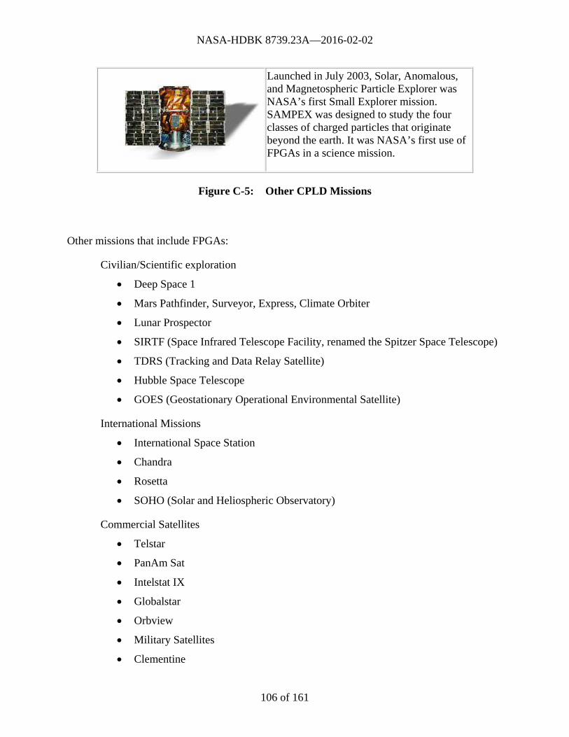
NASA-HDBK 8739.23A—2016-02-02
106 of 161
Launched in July 2003, Solar, Anomalous, and Magnetospheric Particle Explorer was NASA’s first Small Explorer mission. SAMPEX was designed to study the four classes of charged particles that originate beyond the earth. It was NASA’s first use of FPGAs in a science mission.
Figure C-5: Other CPLD Missions
Other missions that include FPGAs:
Civilian/Scientific exploration
Deep Space 1
Mars Pathfinder, Surveyor, Express, Climate Orbiter
Lunar Prospector
SIRTF (Space Infrared Telescope Facility, renamed the Spitzer Space Telescope)
TDRS (Tracking and Data Relay Satellite)
Hubble Space Telescope
GOES (Geostationary Operational Environmental Satellite)
International Missions
International Space Station
Chandra
Rosetta
SOHO (Solar and Heliospheric Observatory)
Commercial Satellites
Telstar
PanAm Sat
Intelstat IX
Globalstar
Orbview
Military Satellites
Clementine

NASA-HDBK 8739.23A—2016-02-02
107 of 161
HESSI (High Energy Solar Spectroscopic Imager)
Mighty Sat
SBIRS-High (-Low) (Space Based Infrared System)
Launch Vehicles
Ariane
Atlas
Delta
EELV (evolved expendable launch vehicle)
Sea Launch
C.3 ASIC
Device name: Application Specific Integrated Circuit
(ASIC)
Figure C-6: ASIC
Description:
An ASIC, shown in figure C-6, is an integrated circuit designed to perform a particular function by defining the interconnection of a set of basic circuit building blocks drawn from a library provided by the circuit manufacturer. They are built by connecting existing circuit building

NASA-HDBK 8739.23A—2016-02-02
108 of 161
blocks in new ways. Since the building blocks already exist in a library, it is much easier to produce a new ASIC than to design a new chip from scratch.
ASICs are custom-designed integrated circuits, but they are not programmable by the user. They are manufactured (usually in large quantities) by vendors according to the design provided by the customer. If you find a problem with an ASIC after it is produced, the only option is to remanufacture (re-spin) the chip with a corrected device. To avoid costly mistakes, FPGAs are often used to check out and debug the ASIC design prior to submittal to the manufacturer.
While most integrated circuits (ICs) could be considered “application-specific,” because they have a defined purpose, off-the-shelf parts are not really ASICs. They are not designed by the user/customer to incorporate just the required functionality. Examples of ICs that are not ASICs include standard parts such as memory chips (ROMs, DRAM, and SRAM), microprocessors, and all the miscellaneous chips used in modern electronics (FIFOs, logic chips, drivers, clock chips, switches, etc.). Now, if a chip has been designed specifically for a talking toy, a cell phone, or a satellite, it is an ASIC. As a general rule, if found in a data book, then it is probably not an ASIC.
Integrated circuits are made on a thin (a few hundred microns thick), circular silicon wafer, with each wafer holding hundreds of die. The transistors and wiring are made from many layers built on top of one another. Each successive layer has a defined pattern using a mask similar to a glass photographic slide. The first layers define the transistors, and the last layers define the metal wires between the transistors (the interconnections).
ASICs come in two basic varieties, full-custom and semi-custom, which consist of two sub-types: cell-based and gate-array. Each variety or type of ASIC has strengths and weaknesses. A microprocessor is an example of a full-custom ASIC, where each micron on the silicon is customized to give exactly what is needed. Semi-custom ASICs have pre-designed elements and customizable portions.
A full-custom ASIC allows customization of some (and possibly all) logic cells and all mask layers. Customizing all of the ASIC features in this way allows designers to include analog circuits, optimized memory cells, or mechanical structures on an IC, for example. Full-custom ASICs are the most expensive to design and manufacture. The manufacturing lead time (how long it takes to make an ASIC once the design is completed) is typically eight weeks.
Semi-custom ASICs have all of the logic cells pre-designed and some (possibly all) of the mask layers are customized. Designers use pre-designed cells from a cell library, provided by the vendor or a third party. These pre-designed units are usually referred to as IP (Intellectual Property). Semi-custom ASICs are either standard cell-based ASICs or gate-array-based ASICs.
A cell-based ASIC uses pre-designed logic cells (e.g., AND gates, OR gates, multiplexers, and flip-flops) known as standard cells. The standard-cell areas (also called flexible blocks) are built of rows of standard cells like a wall built of bricks. The standard-cell areas may be used in combination with larger pre-designed cells, such as microcontrollers, known as megacells. Megacells are also called megafunctions, full-custom blocks, system-level macros (SLMs), fixed blocks, cores, or Functional Standard Blocks (FSBs).

NASA-HDBK 8739.23A—2016-02-02
109 of 161
The ASIC designer defines only the placement of the standard cells and interconnect in a cell-based ASIC. However, the standard cells can be placed anywhere on the silicon; this means all the mask layers are customized and are unique to a particular customer. The advantages of cell-based ASIC are designers save time, money, and reduce risk by using a pre-designed, pre-tested, and pre-characterized standard-cell library. In addition each standard cell can be optimized individually.
If you were to look through a low-powered microscope at a cell-based ASIC die something similar to Figure C-7 would be seen. This ASIC has a single standard-cell area (a flexible block) together with four fixed blocks. The small squares around the edge of the die are bonding pads that are connected to the pins of the ASIC package.
Figure C-7: ASIC Die
In gate-array-based ASICs, the transistors are predefined on the silicon wafer. This predefined pattern of transistors on a gate array is called the base array, and the smallest element replicated to make the base array is called the base cell. Only the top few layers of metal, which define the interconnect between transistors, are defined by the designer using custom masks.
The designer chooses from a gate-array library of pre-designed and pre-characterized logic cells or macros. The reason is the base-cell layout is the same for each logic cell, and only the interconnect (inside cells and between cells) is customized. Gate-array ASICs can be prefabricated up to a point and stored. At a later time, the final customization steps can be performed to complete the ASIC. This reduces the manufacturing time to only a few days or at most a couple of weeks.
ASIC Cell Libraries
The cell library is the key part of ASIC design. Cell libraries can be provided by the ASIC vendor, procured from a third-party library vendor, or custom-built. The first choice, using an ASIC-vendor library, requires the use of a set of design tools approved by the ASIC vendor to enter and simulate your design. An ASIC vendor library is normally a phantom library - the cells are empty boxes, or phantoms, but contain enough information for layout. After layout is completed a netlist is sent to the ASIC vendor, who fills in the empty boxes (phantom instantiation) before manufacturing your chip.
The second and third choices requires a buy-or-build decision. If an ASIC design is done using a purchased cell library, you also own the masks (the tooling) used to manufacture the ASIC. This is called customer-owned tooling (COT, pronounced “see-oh-tee”). A library vendor normally

NASA-HDBK 8739.23A—2016-02-02
110 of 161
develops a cell library using information about a process supplied by an ASIC foundry. An ASIC foundry (in contrast to an ASIC vendor) only provides manufacturing, with no design help. If the cell library meets the foundry specifications, it is considered to be a qualified cell library. These cell libraries are normally expensive (possibly several hundred thousand dollars), but if a library is qualified at several foundries this allows the developer to shop around for the most attractive terms. This means buying an expensive library can be cheaper in the long run than the other solutions for high-volume production.
The third choice is to develop a cell library in-house. Many large computer and electronics companies make this choice. Most of the cell libraries designed today are still developed in-house despite the fact the process of library development is complex and very expensive.
However created, each cell in an ASIC cell library must contain the following:
A physical layout,
A behavioral model,
A Verilog/VHDL model,
A detailed timing model,
A test strategy,
A circuit schematic,
A cell icon,
A wire-load model, and
A routing model.
Applications:
ASICs are used widely in many types of electronics devices. Anytime there are a large number of devices manufactured that require specialized operation, an ASIC is probably inside.
ASICs application examples include:
Battery management for household appliances,
Low noise audio circuit,
Analog Integrated Circuit for industrial environment,
Sensitive photo transistors and opto-sensors,
DC-DC converters from 0.9V supply voltage,
Control circuit for cycle rear light,
120V Linear Regulator,
Interface circuit for a bar code reader,

NASA-HDBK 8739.23A—2016-02-02
111 of 161
Control and evaluation circuit for motion detectors,
Timer electronics,
Interface and signal processing electronics for sensors (light, vibration and magnetic field),
Control circuit for mobile phones,
Automotive control functions, and
PDAs.
NASA Examples:
ASICs can provide several features that are especially important in spacecraft and instruments, such as:
Customized electronics,
Smaller footprint,
Less weight, and
Hard-coded (radiation resistant).
The smaller footprint on the circuit board and reduced weight are the result of including multiple functions in a single chip, rather than having to use many individual integrated circuit chips.
Figure C-8: Cassini
See section C.2 also. The Cassini spacecraft, see Figure C-8, is a complicated system, with 22,000 wire connections and nearly nine miles of cabling. The main on-board computer uses very high-speed ICs and advanced, radiation-hardened ASICs. Each ASIC replaces one hundred or more traditional chips, allowing the development of a data system for Cassini that is ten times more efficient than earlier spacecraft designs (e.g., Galileo and Magellan),
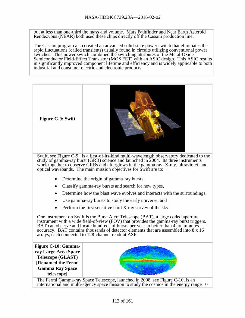
NASA-HDBK 8739.23A—2016-02-02
112 of 161
but at less than one-third the mass and volume. Mars Pathfinder and Near Earth Asteroid Rendezvous (NEAR) both used these chips directly off the Cassini production line.
The Cassini program also created an advanced solid-state power switch that eliminates the rapid fluctuations (called transients) usually found in circuits utilizing conventional power switches. This power switch combined the switching attributes of the Metal-Oxide Semiconductor Field-Effect Transistor (MOS FET) with an ASIC design. This ASIC results in significantly improved component lifetime and efficiency and is widely applicable to both industrial and consumer electric and electronic products.
Figure C-9: Swift
Swift, see Figure C-9, is a first-of-its-kind multi-wavelength observatory dedicated to the study of gamma-ray burst (GRB) science and launched in 2004. Its three instruments work together to observe GRBs and afterglows in the gamma ray, X-ray, ultraviolet, and optical wavebands. The main mission objectives for Swift are to:
Determine the origin of gamma-ray bursts,
Classify gamma-ray bursts and search for new types,
Determine how the blast wave evolves and interacts with the surroundings,
Use gamma-ray bursts to study the early universe, and
Perform the first sensitive hard X-ray survey of the sky.
One instrument on Swift is the Burst Alert Telescope (BAT), a large coded aperture instrument with a wide field-of-view (FOV) that provides the gamma-ray burst triggers. BAT can observe and locate hundreds of bursts per year to better than 4 arc minutes accuracy. BAT contains thousands of detector elements that are assembled into 8 x 16 arrays, each connected to 128-channel readout ASICs.
Figure C-10: Gamma-ray Large Area Space Telescope (GLAST) [Renamed the Fermi Gamma Ray Space
telescope]
The Fermi Gamma-ray Space Telescope, launched in 2008, see Figure C-10, is an international and multi-agency space mission to study the cosmos in the energy range 10

NASA-HDBK 8739.23A—2016-02-02
113 of 161
keV - 300 GeV. Fermihas an imaging gamma-ray telescope vastly more capable than instruments flown previously, as well as a secondary instrument to augment the study of gamma-ray bursts. The main instrument, the Large Area Telescope (LAT), has superior area, angular resolution, and field of view over previous instruments. The LAT tracker subsystem was focused on compactness, minimum wiring, and redundancy. The subsystem was implemented using two ASICs.
SonoSite’s TITAN™ system took part in a 10-day underwater experiment with NASA Extreme Environment Mission Operations (NEEMO) 7 Mission. Aquanauts used the laptop-sized ultrasound system to scan each other in simulated emergency situations and transmit live images to a hospital for review by radiologists. The TITAN system utilizes SonoSite's proprietary ASIC microchip technology to integrate millions of transistors onto one circuit.
NASA's Jet Propulsion Laboratory has developed a command interface ASIC and an analog interface ASIC. This chip set for remote actuation and monitoring of a collection of switches can be used to control generic loads, pyrotechnic devices, and valves in a high-radiation environment. The command interface ASIC (CIA) can be used alone or in combination with the analog interface ASIC (AIA). Designed primarily for incorporation into spacecraft control systems, they are also suitable for use in high-radiation terrestrial environments (e.g., in nuclear power plants and facilities that process radioactive materials).
C.4 SoC
Device name: System-on-Chip (SoC)
Also known as System-on-a-chip (SoaC)
Figure C-11: SOC

NASA-HDBK 8739.23A—2016-02-02
114 of 161
Description:
The SoC depicted in figure C-11, also called “system-on-a-chip” or SoaC, is a complete product containing all the necessary electronic circuits and parts for a "system" on a single integrated circuit. Think of it as a single-board-computer on a chip. SoCs include the hardware components and all required ancillary electronics. SoCs combine aspects of ASICs and field-programmable logic. SoCs can be:
Totally ASIC, with the individual blocks specified by the designer;
ASIC for the computing unit and logic functions, with some programmable parts (e.g., CPLD); and
Implemented on programmable logic (e.g., FPGA).
SoCs can use IP designs created by others and integrated into the chip. IP blocks are pre-designed behavioral or physical descriptions of a standard component. These reusable components are usually Commercial-off-the-Shelf (COTS) products.
The benefits of SoC design include:
Conservation of space (reduction in chip count),
Improved performance (higher reliability),
Lower memory requirements, and
Greater design freedom (simpler logistics).
These benefits also come with some challenges including:
Larger design space,
More expense (global on-chip communication is expensive in terms of power/propagation delay),
Increased prototype cost,
Correctness of complete system with multiple components, and
A high level of debugging methodology.
Testing of the products is also a challenge due to the fact that typical testing methods have been developed for specific specialty areas, whereas the SoC requirement includes all specialties, potentially on one platform.
A SoC could include:
Microprocessor,
Memory (e.g., SRAM, DRAM, Flash),
Communications cores,

NASA-HDBK 8739.23A—2016-02-02
115 of 161
Digital Input/Output functions,
Analog Input/Output functions,
Bus controllers (e.g., PCI (Peripheral Component Interconnect)),
DSP (Digital Signal Processor),
Sensors,
Programmable logic (e.g., FPGA, CPLD), and
Embedded software.
For example, a system-on-chip for a sound-detecting device might include an audio receiver, an analog-to-digital converter (ADC), a microprocessor, necessary memory, and the input/output logic control for a user - all on a single microchip.
Configurable System-on-Chip (CSoC)
Configurable SoCs are a new form of system-on-chip that has a configurable fabric designers’ can manipulate, after chip fabrication, to achieve specific functionality. Configurability lets the on-chip functions be changed for a variety of reasons. These reasons include:
Change in core functionality,
Compatibility with a change in a communications or other standard to which the CSoC must conform, and
Correcting a design error incurred during original chip development.
Post-process configurability lets the designer create products that can adapt to changing requirements.
Some configurable SoCs are FPGAs that combine both hard (fixed) and soft (programmable) cores. These chips are sometimes referred to as platform FPGAs. In figure C-12 below, the microprocessor is a hard component (fixed in the silicon), while the Digital Signal Processor (DSP) is a soft component created in the FPGA programmable infrastructure.
The reconfigurable approach offers significant advantages. It reduces design costs because changes can be made immediately to the chip during development. Chip simulation becomes less of an issue because the real hardware is available immediately. In the field, bug fixes and upgrades can be more extensive as significant portions of the hardware can be altered, not just the application code.

NASA-HDBK 8739.23A—2016-02-02
116 of 161
Figure C-12: Reconfigurable SoC
Cost is the main downside to using a standard reconfigurable SoC rather than creating a custom SoC. Custom designs typically have large up-front development costs, but low individual chip costs. Reconfigurable SoCs have a comparatively small up-front cost, but are usually more expensive per chip. Reconfigurable SoCs can also be used for prototyping because the core CPU and fixed peripherals are well defined. Building a custom ASIC or SoC based on a reconfigurable prototype is relatively easy.
Applications for SoC:
System-on-chip devices can be used in any application requiring a processor and peripheral components. Since the advantages of SoC are small size, integrated components, and reduced power, they are especially useful in:
Cell/camera phones,
Medical equipment (especially portable devices),
Portable multimedia devices,
Network-enabled devices,
PDAs,
Point-of-sale devices, and
Gaming systems.
In the medical world, portable equipment and implantable devices are becoming more common. Such equipment includes blood glucose monitoring systems, insulin pumps, body temperature sensors, defibrillators, neurological stimulators, pacemakers, and hearing aids. These products not only simplify the testing, monitoring, and treatment processes, but can also help to improve the quality of life for the patient by minimizing time spent in hospitals and often providing automatic, continuous treatment of chronic conditions.

NASA-HDBK 8739.23A—2016-02-02
117 of 161
To address requirements for performance, power consumption, and size, medical equipment manufacturers are incorporating as much functionality as possible into a single, complex SoC. These devices need to integrate both analog and digital capabilities and, in many cases, deliver short-range, low-data-rate wireless communication functionality. Furthermore, some applications may also require high-voltage output stages be integrated into the same device. A variety of semiconductor technologies, IP blocks, and support tools can significantly simplify implementation of SoCs for implantable and portable medical devices.
An example of a network device is the Sony Video Network Station. This device, which contains an embedded Linux operating system running on an Axis ETRAX system-on-chip processor, transmits images generated by analog video cameras to remote locations where they can be viewed using ordinary GUI-based (Graphical User Interface) web browsers. The device is useful in a diverse range of applications requiring remote video monitoring and control, including security monitoring, quality inspection, image distribution, access control, and market research.
NASA projects:
Like ASICs and FPGAs, SoC devices have significant benefits for NASA projects, including:
Customizable electronics,
Smaller circuit board footprint,
Less weight, and
Integrated functionality.
Temperature Remote I/O (TRIO) System-on-Chip for Aerospace
The TRIO smart sensor data acquisition chip was developed by Johns Hopkins University/Applied Physics Laboratory for NASA spacecraft applications. TRIO includes a 10 bit self-corrected analog-to-digital converter, analog inputs, a front end multiplexer with selectable acquisition time, a current source, memory, serial and parallel bus, and control logic. These functions are very useful for spacecraft and subsystems health and status monitoring and control actions. The key contributions of the TRIO are feasibility of modular architectures, elimination of several miles of wire harnessing, and power savings by orders of magnitude. So far TRIO is used in many missions including Contour, Messenger, Stereo, Europa Orbiter, Mars Surveyor Program, Solar Probe, Pluto Express, and in the generic JPL X2000 spacecraft bus.
Radio Frequency (RF) components
Micro-Electro-Mechanical Systems (MEMS) integrate mechanical elements, sensors, actuators, and electronics on a common silicon substrate through microfabrication technology. Microelectronic integrated circuits can be thought of as the "brains" of a system and MEMS augments this decision-making capability with "eyes" and "arms” to allow microsystems to sense and control the environment.

NASA-HDBK 8739.23A—2016-02-02
118 of 161
NASA Glenn Research Center is developing microwave MEMS devices that integrate with miniature microwave (RF) transmission lines and components to build low loss RF distribution networks for System on a Chip (SOAC) and phase array antennas. These novel, low loss, miniature RF components will be fabricated using multilayer processing, and they will be combined with SOAC technology being developed by the University of Michigan and the JPL Center for Integrated Space Microsystems (CISM) for nano-sized science craft.
Advanced time-of-flight system-on-chip for remote sensing instruments
Accurate and/or fast time interval measurement is important in many remote sensing instruments, especially those requiring detection of photon/particle events, position decoding and time-of-hit measurement. An advanced time-of-flight (TOF) system-on-chip has been developed that includes the complete signal processing electronics for microchannel plate (MCP) readout. The TOF chip is capable of a time resolution of <50 picoseconds. The TOF chip was used on the NASA/IMAGE spacecraft launched in 2000 and is part of many other science instruments on MESSENGER.
ChipSat
ChipSat is a long-term research program which aims to build a satellite-on-a-chip. As part of the program, an existing on-board computer (OBC) was scaled down to a SoC. The OBC chosen was developed by the Surrey Satellite Technology Limited (SSTL), a company owned by the University of Surrey in Guildford, UK. The SoC is prototyped on a single high-density programmable logic array chip using soft IP cores.
Figure C-13 shows the parts of the OBC that were mapped into the system-on-chip. An entire board was shrunk down to a single chip. The experiment showed that it is possible to implement the functionality of a small satellite OBC on a single programmable logic chip.
SCOC – A Spacecraft Controller On a Chip
The European Space Agency (ESA) is pursuing development of a system-on-chip incorporating all the required functions for spacecraft control. This SoC is currently prototyped in an FPGA. The demonstration board is named BLADE (Development of the Board for LEON and Avionics DEmonstration). Eventually, the design will be produced in a radiation-tolerant ASIC or PROM-based FPGA.
SCOC looks to integrate multiple functions into a single chip. By integrating the functions, the external connections become on-chip interconnects. Other benefits include reduced power consumption, reduced component count (and thus lower mass), and increased performance and reliability. However, putting all the functions on a single chip reduces the accessibility to the internal functions and makes testing the complex chip more difficult.

NASA-HDBK 8739.23A—2016-02-02
119 of 161
Figure C-13: ChipSat OBC
The SCOC will include the following components:
Standard processor, known to the space community (the LEON SPARC-V8),
Flexible peripherals, which can be powered down,
Telecommand and Telemetry (TM/TC) functionality (using the CCSDS protocol),
Housekeeping and CCSDS Time Management,
Multiple standard interfaces,
PCI parallel backbone,
Spacewire (IEEE 1355.1),
MIL 1553 standard Bus Controller/Monitor (BC/BM) and Remote Terminal (RT),
Dedicated data processing,
Monitoring camera interface and image compression,
GNSS navigation receiver,
Star tracker pre-processor, and
Mathematical co-processor.
The current BLADE development integrates the processor with standard interfaces. Additional functionality will be added in the future.

NASA-HDBK 8739.23A—2016-02-02
120 of 161
C.5 Reconfigurable Computing
Device name: Figure C-14: Reconfigurable Computing
AKA Adaptable Computing, Evolvable computing
Description:
Is a computer without a microprocessor possible? How can the hardware deal with situations where autonomous instruments have to adapt to changing situations? What if the device has to support multiple protocols, depending on its location or mission? How can the hardware process signals that may come in multiple formats without advance planning?
The answer to the questions above is “reconfigurable computing”, see Figure 14. Reconfigurable Computing represents a new idea in computing philosophy, in which some general-purpose hardware agent is configured to carry out a specific task, but can be reconfigured on-demand to carry out other specific tasks.
Traditionally, there have been two ways to implement a computation or algorithm: custom hardware or software. In some systems, this decision can be made on an individual subtask basis, placing some subtasks in custom hardware and some in software on more general-purpose processing engines.
Hardware designs offer high performance because they are:
Customized to the problem - No extra overhead for interpretation or extra circuitry capable of solving a more general problem, and
Relatively fast - Due to their highly parallel and spatial execution.

NASA-HDBK 8739.23A—2016-02-02
121 of 161
Software implementations exploit a “general-purpose” execution engine (i.e., microprocessor), which interprets a designated data stream as instructions telling the engine what operations to perform. As a result, software is:
Flexible - Task can be changed simply by changing the instruction stream,
Relatively slow - Due to mostly temporal, serial execution, and
Relatively inefficient - Since operators can be poorly matched to computational task.
Reconfigurable computing combines the best of both implementations, allowing general-purpose software to be implemented in hardware. This class of architectures permits the computational capacity of the system to be highly customized to the instantaneous needs of an application, while also allowing the computational capacity to be reused in time at a variety of time scales.
The usual hardware agent for reconfigurable computing is a set of FPGAs. Reconfigurable computing manipulates the logic within the FPGA at run-time. The design of the hardware may change in response to the demands placed upon the system while it is running. Here, the FPGA acts as an execution engine for a variety of different hardware functions, some executing in parallel, others in serial, much as a microprocessor executes a variety of software threads.
Reconfigurable computing offers several advantages over custom hardware and general-purpose software implementations, including:
Flexibility - The system can be changed as necessary, on the fly,
Simpler hardware design - Does not need a fancy high-powered microprocessor, just one or more FPGAs, and
Speed - Implementing algorithms in hardware results in faster execution, due to the parallel nature of hardware.
The reconfigurable computing systems built during the last years have often achieved performance several orders of magnitude higher than the traditional processor based solutions. Reconfigurable computing is now breaking into the commercial market in the areas of application-specific systems and information appliances, which include emerging areas like mobile communication, multimedia-based networks, encryption, and image processing.
What hardware is reconfigurable?
Not all FPGAs can be used in reconfigurable computing. User-configurable FPGAs can be programmed and reprogrammed by the user in a lab, or even in the field, but they cannot be dynamically reprogrammed as the system is running. Many older FPGAs read their configuration out of a serial EEPROM, and only when a chip reset signal is asserted. This means the FPGA must be reprogrammed in its entirety and its previous internal state cannot be captured beforehand.
In order to benefit from run-time reconfiguration, the FPGAs involved need some or all of the following features, which increase design flexibility:

NASA-HDBK 8739.23A—2016-02-02
122 of 161
On-the-fly reprogrammability - Resetting the FPGA takes a lot of time and should be avoided whenever possible.
Partial reprogrammability - The ability to leave most of the internal logic in place and change just one part is an important factor in reconfigurable systems. It will always be much faster to change a small piece of the logic than the entire FPGA contents.
Externally-visible internal state - If you can see the internal state of the FPGA at any time, then it is also possible to capture that state and save it for later use. This allows the internal state of the FPGA to be read and written just like memory or processor registers and makes it possible to swap hardware designs in much the same way that pages of virtual memory are swapped into and out of physical memory.
Run-time environments
How does the reconfigurable system know what to do at any given time? That job is usually handled by software. The software manages the processes of:
Deciding which hardware objects to execute and when,
Swapping hardware objects into and out of the reconfigurable logic, and
Performing routing between hardware objects or between hardware objects and the hardware object framework.
When software manages the reconfigurable hardware it usually means having an embedded processor or microcontroller on-board. The embedded software that runs there is called the run-time environment and is analogous to the operating system that manages the execution of multiple software threads. Like threads, hardware objects may have priorities, deadlines, and contexts. It is the job of the run-time environment to organize this information and make decisions based upon it.
Using software allows developers to write applications at a very high level of abstraction. For example, if the software needed to decompress an image, the attached FPGA could be reconfigured with the decompression algorithm and fed the data. To the main software application, this action is no different than asking an analog-to-digital converter to read a voltage and return the answer. The run-time environment software, however, is responsible for reprogramming the FPGA and executing the task.
Programming reconfigurable systems
Reconfigurable computing combines traditional software-related topics as languages, compilers, operating systems, and libraries with hardware-related topics of digital design.
Reconfigurable systems present a formidable challenge in terms of algorithm design tools. Design tools for FPGA devices, the building blocks of reconfigurable hardware, are oriented towards ASIC development environments, in which digital design engineers create large (multi-

NASA-HDBK 8739.23A—2016-02-02
123 of 161
million gate), complex designs that, once created and validated, do not change. In contrast, reconfigurable supercomputers require a more software-centric development environment, in which algorithms are constantly revised and tested.
In response to the need for software-oriented tools, vendors and researchers have developed compilers for software programming languages that synthesize hardware. Compilers for several C variants, Java, and Matlab have become available in the past few years. The compiler must generate a structural hardware representation (such as VHDL-RTL) that represents the connections between units contained in a library, with direct correspondence to the operators of high-level programming languages.
Applications:
While commercial reconfigurable computing platforms are starting to become available, the majority of work has been done in a research context. There are some areas and problems that reconfigurable computing is ideal for, including:
Real-time image analysis,
Pattern recognition,
Automatic target recognition,
Cryptography,
Computational biology, and
Signal processing.
One theoretical application is a smart cellular phone that supports multiple communication and data protocols, though just one a time. When the phone passes from a geographic region served by one protocol into a region served by another, the hardware is automatically reconfigured. This is reconfigurable computing at its best. Using this approach, it is possible to design systems that do more, cost less, and have shorter design and implementation cycles.
Heading into the future, evolvable hardware (EHW) is designed to adapt to changes in task requirements or changes in the environment through its ability to reconfigure its own hardware structure dynamically and autonomously. This capacity for adaptation is achieved by employing efficient search algorithms known as genetic algorithms. Evolvable hardware has great potential for the development of innovative applications, including autonomous spacecraft and exploration systems.
Here are some reasons why reconfigurable computing has valuable applications for space missions:
After launch, unmanned spacecraft electronics are generally unavailable for physical upgrade or repair. RC technology allows new hardware circuits to be uploaded via a radio link.

NASA-HDBK 8739.23A—2016-02-02
124 of 161
New circuit configurations can overcome design faults, allow improved processing algorithms to be uploaded, or change system functionality in response to changing mission requirements. Combined with artificial intelligence applications, the unmanned spacecraft may be able to select circuits on its own to correct the problems.
The same circuitry can be used with different configurations at different stages of a mission, reducing weight and power requirements.
If part of an FPGA fails, then circuitry can be reprogrammed to make use of remaining functional portions of the chips.
Use of FPGAs allows generic circuit boards to be designed, which are customized for individual applications. This helps overcome the very high NRE (non-recurring engineering) costs associated with small volume spacecraft design. Physical and environmental qualification costs can also be shared across many missions.
In-flight reconfiguration provides additional safety margins for missions with very short lead-times, or for those where mission requirements are not fully defined at launch.
NASA Examples:
NASA Langley Research Center is one NASA installation exploring reconfigurable computing applications. They have developed a reconfigurable FPGA-based research hypercomputer capable of performing comprehensive engineering and scientific calculations. Two approaches have been adopted to exploit Langley’s Star Bridge Systems HC-38 (and 2 HAL15s) for analysis calculations:
1. Rewrite legacy code for the hypercomputer to fully exploit parallelism.
2. Use the hypercomputer to accelerate time-consuming (bottleneck) calculations.
Software was entirely rewritten from C++ or FORTRAN to take advantage of the parallelism inherent in the hypercomputer (approach 1). When only a small portion of a software application was computationally intensive, that portion was rewritten to the hypercomputer native language, and the rest of the code was left alone (approach 2).
FedSat, an Australian science and engineering research satellite, was launched in 2002. One payload on FedSat is the Adaptive Instrument Module (AIM), which is a reconfigurable computer optimized for spacecraft instrument use. AIM has demonstrated autonomous instrument processing that is reconfigurable and adaptive. The use of the AIM enables reconfiguration of the FPGA circuitry while the spacecraft is in flight. This flexibility reduces mission risk, especially for missions with a very tight development schedule. The AIM is designed to either directly interface with sensors or instruments or to receive data through the spacecraft data handling system. AIM conducted a series of designed experiments, including a

NASA-HDBK 8739.23A—2016-02-02
125 of 161
demonstration of implementing data compression, data filtering, and communication message processing and inter-experiment data computation.
The design of the AIM specifically addresses the concerns of using SRAM-based FPGAs in the space environment. The AIM demonstrates techniques to detect and remediate radiation-induced upsets in these FPGAs and will automatically restart in the event of an upset. The design has been proven in flight. When the module suffered a memory error due to the bombardment of cosmic radiation, AIM automatically detected and then reset itself. This prevented the memory error from causing an error in the data it was processing.
The AIM development team at the Applied Physics Laboratory/John Hopkins University is working with NASA’s Langley Research Center to take the next step in reconfigurable, self-repairing space borne computer design. The project is called ADAPT – Adaptive Data Analysis and Processing Technology. Because it is fully reconfigurable, an ADAPT computer can serve as the front-end package for virtually any type of instrument – for example, a spacecraft might carry six scientific instruments, each served by a physically identical, but differently programmed, ADAPT computer. As the design evolves, an ADAPT computer may carry up to 20 preprogrammed operating modes for controlling its instrument.

NASA-HDBK 8739.23A—2016-02-02
Material presented in Appendix Dis based on or adapted from figures and text copyrighted by Xilinx, Inc., and used with permission.
126 of 161
APPENDIX D CODING STYLE GUIDELINES
Note: Material presented in Appendix D is based on or adapted from figures and text copyrighted by Xilinx, Inc., and used with permission.
D.1 Introduction
This document was created to provide Xilinx users with a guideline for producing fast, reliable, and reusable HDL code.
D.2 Top-Down Design
HDL coding should start with a top-down design approach. Use a top-level block diagram to communicate to designers the naming required for signals and hierarchical levels. Signal naming is especially important during the debug stage. Consistent naming of signals, from top to bottom, will ensure that project manager A can easily recognize the signals written by designer B.
D.2.1 Behavioral and Structural Code
When creating synthesizable code (RTL), you should write two types of code: behavioral RTL (leaf-level logic inference, sub-blocks) and structural code (blocks) -- each exclusively in its own architecture. A simple example of behavioral RTL versus structural code is shown in Figure D-1and Figure D-2, respectively.
Figure D-1: Behavioral Code
entity mux2to1 is port ( a : in std_logic_vector(1 downto 0); sel : in std_logic; muxed : out std_logic);end mux2to1;
architecture rtl of mux2to1 isbegin
muxed <= a(1) when sel = '1' else a(0);
end rtl;

NASA-HDBK 8739.23A—2016-02-02
Material presented in Appendix Dis based on or adapted from figures and text copyrighted by Xilinx, Inc., and used with permission.
127 of 161
Figure D-2: Structural Code
Rules
Keep leaf-level (behavioral sub-blocks) coding separate from structural coding (blocks).
Declarations, Instantiations, and Mappings. It is important to use a consistent, universal style for such things as entity declarations, component declarations, port mappings, functions, and procedures.
D.2.2 Declarations, Instantiations, and Mappings
It is important to use a consistent, universal style for such things as entity declarations, component declarations, port mappings, functions, and procedures.
Rules
entity mux4to1 is port ( input : in std_logic_vector(3 downto 0); sel : in std_logic_vector(1 downto 0); muxed : out std_logic);end mux4to1;
architecture structural of mux4to1 is signal muxed_mid : std_logic_vector(1 downto 0); component mux2to1 port ( a : in std_logic_vector(1 downto 0); sel : in std_logic; muxed : out std_logic); end component;begin
mux2to1_1_0: mux2to1 port map ( a => input(1 downto 0), sel => sel(0), muxed => muxed_mid(0)); mux2to1_3_2: mux2to1 port map ( a => input(3 downto 2), sel => sel(0), muxed => muxed_mid(1)); mux2to1_final: mux2to1 port map ( a => muxed_mid, sel => sel(1), muxed => muxed);end structure;

NASA-HDBK 8739.23A—2016-02-02
Material presented in Appendix Dis based on or adapted from figures and text copyrighted by Xilinx, Inc., and used with permission.
128 of 161
For declarations, instantiations, and mappings use one line for each signal. The exception is for relatively small components, functions, and procedures.
Always use named association.
The combination of these two rules will help eliminate common coding mistakes. Therefore, this combination will greatly enhance the ease of debugging a design at every stage of verification. A simple example is shown Figure D-3. Obeying these rules will also increase the readability, and therefore the reusability.
Figure D-3: One Line Per Signal/Named Association
D.2.3 Comments
Liberal comments are mandatory to maintain reusable code. Although VHDL is sometimes considered to be self-documenting code, it requires liberal comments to clarify intent, as any VHDL user can verify.
Rules
Three primary levels of commenting:
Comments should include a header template for each entity-architecture pair and for each package- and package-body pair. See the example in Figure D-4. The purpose should include a brief description of the functionality of each lower block instantiated within it.
Use comment headers for processes, functions, and procedures, as shown Figure D-5. This should be a description of the purpose of that block of code.
Use comments internal to processes, functions, and procedures to describe what a particular statement is accomplishing. While the other two levels of commenting should always be included, this level is left to the designer to decipher what is required to convey intent. Inline comments are shown in Figure D-6.
architecture structural of mux4to1 is . . . begin
mux2to1_1_0: mux2to1 port map ( a => input(1 downto 0), sel =>sel(0)

NASA-HDBK 8739.23A—2016-02-02
Material presented in Appendix Dis based on or adapted from figures and text copyrighted by Xilinx, Inc., and used with permission.
129 of 161
Figure D-4: Header Template
Figure D-5: Process, Function, and Procedure Header
--------------------------------------------------------------------------------------------------------------------------------------------------------- Author: John Q. Smith Copyright Xilinx, 2001-- Xilinx FPGA - VirtexII-- Begin Date: 1/10/01-- Revision History Date Author Comments-- 1/10/01 John Smith Created-- 1/14/01 John Smith changed entity port address & data to addr & dat--------------------------------------------------------------------------------------------------------------------------------------------------------- Purpose:-- This entity/architecture pair is a block level with 4 sub-blocks. This is the processor control interface for the-- block level <block_level_A>. So on, and so forth…-------------------------------------------------------------------------------------------------------------------------------------------------------
-------------------------------------------------------------------------------------------------- demux_proc: this process dumultiplexes the inputs and registers the-- demultiplexed signals------------------------------------------------------------------------------------------------demux_proc : process(clk, reset)begin …
-------------------------------------------------------------------------------------------------- demux_proc: this process dumultiplexes the inputs and registers the-- demultiplexed signals------------------------------------------------------------------------------------------------demux_proc : process(clk, reset)begin …if reset = ‘1’ then demux <= (others => ‘0’);elsif rising_edge(clk) then -- demultiplex input onto the signal demux case (sel) is when ‘0’ => demux(0) <= input; when ‘1’ => demux(1) <= input; when others => demux <= (others => ‘0’); end case;end if;end process;

NASA-HDBK 8739.23A—2016-02-02
Material presented in Appendix Dis based on or adapted from figures and text copyrighted by Xilinx, Inc., and used with permission.
130 of 161
Figure D-6: Inline Comments
D.2.4 Indentation
Proper indentation ensures readability and reuse. Therefore, a consistent style is warranted. Many text editors are VHDL-aware, automatically indenting for “blocks” of code, providing consistent indentation. Emacs and CodeWright are two of the most common editors that have this capability. Figure D-7 shows an example of proper indentation. Proper indentation greatly simplifies reading the code. If it is easier to read, it is less likely that there will be coding mistakes by the designer.
Rules
Use a VHDL-aware text editor that provides a consistent indentation style.
Figure D-7: Proper Indentation
-- purpose: to show proper indentation
sample_proc : process (clk, reset)
variable muxed_data_v : std_logic_vector (1 downto 0); -- _v denotes a variable
begin -- process sample_proc
if reset = '0' then
for i in data'range loop
data(i) <= (others => '0'); -- data is a 4x2 array
end loop; -- i
muxed_data <= '0'
elsif clk'event and clk = '1' then
muxed_data_v := data(conv_integer(addr));
case sel is
when '0' =>
muxed_data <= mux_data_v(0);
when '1' =>
muxed_data <= mux_data_v(1);
end case; -- case sel is
end if; -- if reset = ‘0’…
end process sample_proc;

NASA-HDBK 8739.23A—2016-02-02
Material presented in Appendix Dis based on or adapted from figures and text copyrighted by Xilinx, Inc., and used with permission.
131 of 161
D.2.5 Naming Conventions
Naming conventions maintain a consistent style, which facilitates design reuse. If all designers use the same conventions, designer A can easily understand and use designer B’s VHDL code.
D.2.6 Entities, Architectures, Procedures, and Functions
Rules
Use all lowercase names with underscores, for readability and name delimiting.
Each entity should have a unique name that describes that block.
Architectures do not need unique names because they are individually bound to a specific entity that has a unique name. Names for architectures should be rtl, to indicate a leaf-level sub-block, and structural, to indicate a block with no leaf-level logic – with only sub-blocks.
For entities with more than one architecture, use “rtl_xilinx” (or “structural_xilinx”) for a Xilinx-specific architecture and “rtl_asic” (or “structural_asic”) for an ASIC-specific architecture.
D.2.7 Signal Naming Conventions
For a design implemented in VHDL, an up-front specification of signal naming conventions should help you reduce the amount of non-conformity. The primary motivating factor is enhanced readability during the verification of the design. General signal naming conventions are listed below.
General Signal Naming Guidelines
Use addr for addresses. This might include sys_addr, up_addr, etc.
Use clk for clock. This might include clk_div2 (clock divided by 2), clk_x2 (clk multiplied by 2), etc.
Use reset or rst for synchronous reset.
Use areset or arst for asynchronous reset.
Use areset_l for active-low asynchronous reset.
Use rw_l for read/write (write is active low).
Rules
The following rules specify the suggested nomenclature for other widely used signals
Use <signal_name>_io for bi-directional signals.
Use a _l suffix for active low signals <signal_name>_l.

NASA-HDBK 8739.23A—2016-02-02
Material presented in Appendix Dis based on or adapted from figures and text copyrighted by Xilinx, Inc., and used with permission.
132 of 161
Do not use _in and _out suffixes for port signal names.
Use of in and out is very confusing in text, especially at hierarchical boundaries. Therefore, the use of _in and _out should be strictly monitored. If they must be used, be sure that _in indicates input, and, likewise, that _out is an output to the correct level of hierarchy. Figure D-8 shows an example entity and the instantiation of that entity in a higher block. Here, data_in is connected to data_out, making the code confusing.
Figure D-8: Confusing_in and_out suffixes
Use _i to denote local signal names that are internal representations of an output port. This nomenclature is used to easily identify the internal signal that will eventually be used as an output port.
The counter in Figure D-9 provides a simple example of an output port that cannot be read. The output port count cannot be incremented because it would require count to be read. The problem is solved in the example by incrementing the local internal signal count_i. Some designers try to overcome this problem by using the port as an inout; however, not all synthesis compilers will allow this unless it is three-stated. Declaring the signal to be of type buffer is another common trap. This complicates the code because all signals to which it connects also must be of type buffer. Not all synthesis vendors support the data-type buffer. In addition, data-type buffer does not have all of the required defined functions to perform common arithmetic operations.
entity in_out isport ( data_in : in std_logic_vector (31 downto 0);
data_out : out std_logic_vector(31 downto 0));end entity in_out;…
in_out_inst: in_outport map ( data_in => ram_data_out,
data_out => ram_data_in);
count <= count_i;process (clk, reset)begin if reset = ‘1’ then count_i <= (others => ‘0’); elsif rising_edge(clk) then count_i <= count_i + 1; end if;end process;

NASA-HDBK 8739.23A—2016-02-02
Material presented in Appendix Dis based on or adapted from figures and text copyrighted by Xilinx, Inc., and used with permission.
133 of 161
Figure D-9: Internal Signals Representing Output Ports
Use _v to indicate a variable. Variables can be very useful if used correctly. The _v will serve as a reminder to the designer as to the intent and use of that signal.
Use <signal_name>_p0, <signal_name>_p1, and so forth, to represent a pipelined version of the signal <signal_name> when <signal_name> comes after the pipelining. Use <signal_name>_q0, <signal_name>_q1, and so forth, to represent a pipelined version of the <signal_name> when <signal_name> comes before the pipeline. See Figure D-19 in section 4 for an example of how to use this pipelined signal naming convention.
Append a suffix to signals that use a clock enable and will be part of a clock-enabled path (i.e., multi-cycle path). For example, if the clock enable is enabled only one-quarter of clock cycles, the clock enable should be named to represent that -- ce4. Signals that use this enable might be named <signal_name>_ce4. This will greatly aid you in your ability to specify multi-cycle constraints.
D.3 Signals and Variables
Following some basic rules on the use of signals and variables can greatly reduce common coding problems.
D.3.1 Signals
The rules for using signals are not complex. The most common problem is that signals can be various data types. The problem in VHDL is "casting" from one data type to another. Unfortunately, no single function can automatically cast one signal type to another. Therefore, the use of a standard set of casting functions is important to maintain consistency between designers.
D.3.2 Casting
Rules for Casting
Use std_logic_arith, std_logic_unsigned/std_logic_signed packages.
This provides the essential conversion functions:
conv_integer(<signal_name>): converts std_logic_vector, unsigned, and signed data types into an integer data type.
conv_unsigned(<signal_name>, <size>): converts a std_logic_vector, integer, unsigned (change size), or signed data types into an unsigned data type.
conv_signed(<signal_name>, <size>): converts a std_logic_vector, integer, signed (change size), or unsigned data types into a signed data type.

NASA-HDBK 8739.23A—2016-02-02
Material presented in Appendix Dis based on or adapted from figures and text copyrighted by Xilinx, Inc., and used with permission.
134 of 161
conv_std_logic_vector(<signal_name>, <size>): converts an integer, signed, or unsigned data type into a std_logic_vector data type.
ext(<signal_name>, <size>): zero extends a std_logic_vector to size <size>.
sxt(<signal_name>, <size>): sign extends a std_logic_vector to size <size>.
All conversion functions can take for the <signal_name> data-type a std_logic_vector, unsigned, signed, std_ulogic_vector, or integer. <size> is specified as an integer value.
D.3.3 Inverted Signals
To reduce complication and to make the code easier to debug and test, it is generally recommended that you use active-high signals in hardware description languages. Generally, active-low signals make the code more complicated than necessary. If active-low signals are required at the boundaries of an FPGA, invert incoming signals at the FPGA top structural level. Also, for outbound signals, invert them at the FPGA top structural level. Consider this a rule of thumb.
However, for FPGAs in general and Xilinx FPGAs specifically, inverters are free throughout the device. There are inverters in the IOB, and a LUT can draw in an inverter as part of its functionality, without a loss in performance.
Often, ASIC designers will use active-low signals in their code to use less power in the part. The synthesis tool will map the logic based on a vendor’s libraries. Therefore, the synthesis tool will infer active-low signals internally when it sees fit. For that matter, writing code that uses active-low signals does not necessarily infer active-low signals in the ASIC. Again, the synthesis tool makes these decisions based on the vendor's libraries. Let the synthesis tool do its job.
Rule of thumb
Use only active-high signals in HDL. One exception is a signal with a dual purpose, such as a read or a write signal. In this case, a naming convention should be used to reduce complication – rw_l is an easily recognizable signal name that clearly defines that signal’s role.
Where active-low signals are required, use of a _l as a suffix generally makes the intent clear. E.g., <signal_name>_l. Use of _n is generally confusing.
D.3.4 Rule for Signals
There are a few basic rules to follow when you use signals. Remember that ports are just signals with special rules that apply to them.
D.3.5 Entity Port Rules within the Bound Architecture
You can read from inputs, but you cannot assign to inputs.
You can assign to outputs, but you cannot read from outputs.
See section 1, Signal Naming Conventions, rule number four, for help in skirting this limitation.

NASA-HDBK 8739.23A—2016-02-02
Material presented in Appendix Dis based on or adapted from figures and text copyrighted by Xilinx, Inc., and used with permission.
135 of 161
You can both assign to and read from inouts.
D.3.6 Internal Signal Rules
Never assign to a signal in more than one process, with the exception of a three-state signal.
For a combinatorial process (no registers inferred), never assign to a signal and read from the same signal in the same process. This will eliminate infinite loops when performing behavioral simulation.
This is not true for a "clocked" process; i.e., a process that is used to register signals. A clocked process would only need to have an asynchronous set or reset signal and a clock in its sensitivity list. Therefore, this process would not execute again until there was a change on one of those signals.
In a clocked process, never assign to a signal outside of the control of the if rising_edge(clk) statement (or reset statement if an asynchronous reset exists). This is a common coding mistake. In synthesis, it will infer a combinatorial signal. In a behavioral simulation, it will have the behavior of a signal clocked on the falling edge.
D.3.7 Filling out a Process Sensitivity List
Within a combinatorial process, all signals that are read (which can change) must be in the sensitivity list.
This will insure the correct behavioral simulation. This includes any signals that are compared in if-then-else statements and case statements. It also includes any signal on the right-hand side of an assignment operator. Remember that this is only for signals that can change. A constant cannot change; thus, it does not need to be in the sensitivity list.
Within a clocked process, only an asynchronous set or reset and the clock should be in the sensitivity list.
If others are added, the functionality of a behavioral simulation will still be correct. However, the simulation will be slower because that process will need to be evaluated or simulated whenever a signal in its sensitivity list changes.
D.3.8 Rules for Variables and Variable Use
Variables are commonly not understood and are therefore not used. Variables are also commonly used and not understood. Variables can be very powerful when used correctly. This warrants an explanation of how to properly use variables.
Variables are used to carry combinatorial signals within a process. Variables are updated differently than signals in simulation and synthesis.
In simulation, variables are updated immediately, as soon as an assignment is made. This differs from signals. Signals are not updated until all processes that are scheduled to run in the current

NASA-HDBK 8739.23A—2016-02-02
Material presented in Appendix Dis based on or adapted from figures and text copyrighted by Xilinx, Inc., and used with permission.
136 of 161
delta cycle have executed (generally referred to as suspending). Thus, a variable can be used to carry a combinatorial signal within both a clocked process and a combinatorial process. This is how synthesis tools treat variables – as intended combinatorial signals.
Figure D-10 shows how to use a variable correctly. In this case, the variable correct_v maintains its combinatorial intent of a simple two-input and-gate that drives an input to an or-gate for both the a and b registers.
Figure D-10: Correct Use of Variables
In Figure D-11, you read from the variable incorrect_v before you assign to it. Thus, incorrect_v uses its previous value, therefore inferring a register. Had this been a combinatorial process, a latch would have been inferred.
Figure D-11: Incorrect Use of Variables
process (clk, reset) variable correct_v : std_logic;begin if reset = ‘1’ then a <= ‘0’; b <= ‘0’; elsif rising_edge(clk) then correct_v := c and d; a <= e or correct_v; b <= f or correct_v; end if;end process;
DFF
DFF
B
A
F
E
C
D
correct_v
clk
process (clk, reset) variable incorrect_v : std_logic;begin if reset = ‘1’ then a <= ‘0’; b <= ‘0’; elsif rising_edge(clk) then a <= e or incorrect_v; b <= f or incorrect_v; incorrect_v := c and d; end if;end process;
B
A
F
E
DFF
DFF
incorrect_v
DFF
C
D
clk

NASA-HDBK 8739.23A—2016-02-02
Material presented in Appendix Dis based on or adapted from figures and text copyrighted by Xilinx, Inc., and used with permission.
137 of 161
D.3.9 Rule for Variables
Always make an assignment to a variable before it is read. Otherwise, variables will infer either latches (in combinatorial processes) or registers (in clocked processes) to maintain their previous value. The primary intent of a variable is for a combinatorial signal.
D.4 Packages
Packages are useful for creating modular and reusable code. There should be one or more packages used by a design team. These packages should include commonly used functions, procedures, types, subtypes, aliases, and constants. All team designers should familiarize themselves with the contents of these packages. If each designer were to create his or her own functions, procedures, types, subtypes, aliases, and constants, it could result in code that is difficult for other team members to use and read. Thus, when your team uses packages, it results in code that is more modular and more readable.
Package use can generally be broken down into the three types:
The global package. This package is used on a company-wide basis, on each design. This package should include functions and procedures, such as reduction functions, for instance functions, and procedures that -- and, or, and xor (etc.) -- reduce individual buses. It should also include commonly used types and subtypes. This package should be created in a group setting by VHDL experts (or the most experienced in VHDL) who decide the best elements to have present in the package. This package should be used extensively and should have periodic reviews to determine what should be added to or taken away from the package. Because most divisions within a company work on the same type of projects, primarily, this package should contain the most widely and extensively used material that is common to all design teams.
The project package. This package is used and created for a specific design project. The functions, procedures, types, subtypes, constants, and aliases are all specifically defined and created for the design at hand.
The designer’s packages. These packages are specific to a designer. Packages of this type should not be used extensively. If there is a need for something to be extensively used within the designer’s package, it should be moved into the project package and possibly even the global package. Code readability and modularity is limited by the use of designer packages, as the type of function calls and types, etc. will not be readily understandable to all other designers in the group.
D.4.1 Package Contents
Constants
Used correctly, constants can ease the coding of complex and modular designs. Constants can be used in a variety of ways. They can be used to create ROMs, for modular coding, and to define

NASA-HDBK 8739.23A—2016-02-02
Material presented in Appendix Dis based on or adapted from figures and text copyrighted by Xilinx, Inc., and used with permission.
138 of 161
what or how something should be used. For example, constants can be used in conjunction with generate statements to specify which portion of code to use (synthesize). Consider, for example, one portion of code written for an ASIC implementation and another portion written for a Xilinx implementation. The ASIC implementation should use gates to implement a multiplexer, while the Xilinx version should use three-state buffers to implement a multiplexer. Because some synthesis tools do not currently support configuration statements, a generate statement is the best solution.
Figure D-12 shows an example of how constants can be used to define the logic created. Although this is a simple example, it illustrates the possibilities. By one change to the constant ASIC, an entirely different set of circuitry is synthesized throughout the design.
Figure D-12: A Constant Guiding the Generation of Logic
Constants can aid modular coding. For example, you could define a constant that specifies the width of the address bus. One change to that constant in the package would make a modular change to everything in the design. See Figure D-13. Using constants to define address and data-bus widths may be better than using generics. Generics are passed from the top-down, eliminating the possibility of synthesizing bottom-up. A bottom-up synthesis is generally preferable for decreased synthesis run-times because only the modules that change need to be resynthesized.
--within a packageconstant asic : boolean := True;
…-- within an architecturegenerate_asic :if asic = true thenmux_proc : process (addr, sel, data)
…generate_fpga :if asic = false thentri_state_proc : process (addr, sel, data)
…

NASA-HDBK 8739.23A—2016-02-02
Material presented in Appendix Dis based on or adapted from figures and text copyrighted by Xilinx, Inc., and used with permission.
139 of 161
Figure D-13: Address Width Defined by a Constant
D.4.2 Rules for Defining Constants within a Package
Define constants within a package when it can be used to improve the modularity of the code by guiding generate statements.
Define constants in a package to define sizes and widths of buses. Constants used in this manner are generally more powerful than using generics because it allows the design to be synthesized in any manner, whereas generics allow only top-down synthesis.
Functions and Procedures
By definition, functions and procedures add modularity and reuse to code. Extensive use of functions and procedures from the global and project packages is encouraged. Rather than extensively using functions and procedures from a designer’s package, the designer is encouraged to add the functions and procedures at a local level (within an architecture), to maintain readability for other designers and future reuse.
When defining functions and procedures, it is beneficial to use unsized vectors to pass signals. Using unsized vectors allows a modular use of the subprogram. In addition to using unsized vectors, use signal – range attributes to define the logic.
In the function example shown below in Figure D-14, the input, named vec, is defined as a std_logic_vector. By not defining a sized vector, the actual size of the signal that is passed in will determine the implementation. The range attribute ‘range specifies the size of the intended logic. This function is modular; that is, it is not limited to being used for one specific vector size. A vector of any size can be passed into this function and correctly infer any amount of logic.
--within the package pack_ase_fpgaconstant addrw : integer := 18;
use work.pack_ase_fpga.all;
entity profound isport ( addr : in std_logic_vector (addrw-1 downto 0);
…

NASA-HDBK 8739.23A—2016-02-02
Material presented in Appendix Dis based on or adapted from figures and text copyrighted by Xilinx, Inc., and used with permission.
140 of 161
Figure D-14: Modular Function Use
D.4.3 Rules for Functions and Procedures
Extensive use of functions and procedures is encouraged. Predominately, the functions and procedures should be defined within either the global or the project packages.
Create modular functions and procedures by not specifying the width of inputs and outputs. Then use range attributes to extract the needed information about the size of an object.
Types, Subtypes, and Aliases
Types and subtypes are encouraged for readability. Types defined at the global and project level are generally required, and they help to create reusable code.
Aliases can be used to clarify the intent, or meaning, of a signal. In most cases, the intent of a signal can be clearly identified by its name. Thus, aliases should not be used extensively. While aliases can help to clarify the purpose of a signal, they also add redirection, which may reduce the readability of the code. Although aliases are not used in conjunction only with types and subtypes, it is useful for examples to be included here. In Figure D-15 there are two types defined: a record and an array. For this example, aliases can be used to clarify the use of the signal rx_packet.data (rx_data) and the intent of the signal data_addr(0) (data_when_addr0). In this example, the alias data_when_addr0 is used in place of data_array(0), this provides more meaning to the "slice" of data than data_array(0) provides. Whenever the alias data_when_addr0 is seen in the code, the intent is obvious. The use of the alias rx_data simply provides a shortened version of the signal rx_packet.data while its use and intent are maintained.
function parity (vec : input std_logic_vector) return std_logic is variable temp_parity : std_logic := ‘0’;begin for i in vec’range loop temp_parity := temp_parity xor vec(i); end loop; return temp_parity;end function;
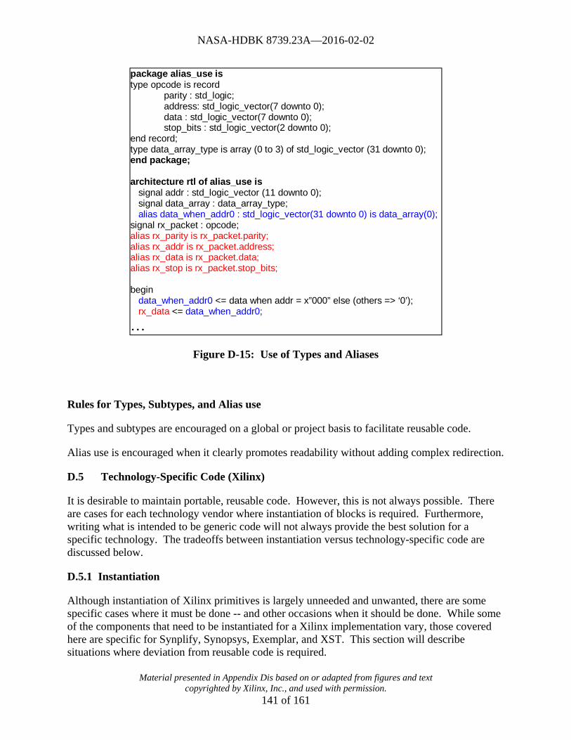
NASA-HDBK 8739.23A—2016-02-02
Material presented in Appendix Dis based on or adapted from figures and text copyrighted by Xilinx, Inc., and used with permission.
141 of 161
Figure D-15: Use of Types and Aliases
Rules for Types, Subtypes, and Alias use
Types and subtypes are encouraged on a global or project basis to facilitate reusable code.
Alias use is encouraged when it clearly promotes readability without adding complex redirection.
D.5 Technology-Specific Code (Xilinx)
It is desirable to maintain portable, reusable code. However, this is not always possible. There are cases for each technology vendor where instantiation of blocks is required. Furthermore, writing what is intended to be generic code will not always provide the best solution for a specific technology. The tradeoffs between instantiation versus technology-specific code are discussed below.
D.5.1 Instantiation
Although instantiation of Xilinx primitives is largely unneeded and unwanted, there are some specific cases where it must be done -- and other occasions when it should be done. While some of the components that need to be instantiated for a Xilinx implementation vary, those covered here are specific for Synplify, Synopsys, Exemplar, and XST. This section will describe situations where deviation from reusable code is required.
package alias_use istype opcode is record
parity : std_logic;address: std_logic_vector(7 downto 0);data : std_logic_vector(7 downto 0);stop_bits : std_logic_vector(2 downto 0);
end record;type data_array_type is array (0 to 3) of std_logic_vector (31 downto 0);end package;
architecture rtl of alias_use is signal addr : std_logic_vector (11 downto 0); signal data_array : data_array_type; alias data_when_addr0 : std_logic_vector(31 downto 0) is data_array(0);signal rx_packet : opcode;alias rx_parity is rx_packet.parity;alias rx_addr is rx_packet.address;alias rx_data is rx_packet.data;alias rx_stop is rx_packet.stop_bits;
begin data_when_addr0 <= data when addr = x”000” else (others => ‘0’); rx_data <= data_when_addr0;
…

NASA-HDBK 8739.23A—2016-02-02
Material presented in Appendix Dis based on or adapted from figures and text copyrighted by Xilinx, Inc., and used with permission.
142 of 161
Required Instantiation
Specific top-level (FPGA) components require instantiation, including the boundary scan component, digital delay-locked loop components (DLL) or digital clock manager (DCM), startup block, and I/O pullups and pulldowns.
Inputs and outputs, other than LVTTL, can be specified in the synthesis tool. However, it is more advantageous to specify the I/O threshold level in the Xilinx Constraints Editor. This will write a constraint into the Xilinx UCF (User Constraint File), which is fed into the Xilinx implementation tools.
To instantiate Xilinx primitives, you will need to have a correct component declaration. This information can be inferred directly from the Xilinx Libraries Guide, found in the online documentation.
D.5.2 Rules for Required Instantiations for Xilinx
Boundary Scan (BSCAN)
Digital Clock Manager (DCM) or Delay-Locked Loop (DLL). Instantiating the DCM/DLL provides access to other elements of the DCM, as well as elimination of clock distribution delay. This includes phase shifting, 50-50 duty-cycle correction, multiplication of the clock, and division of the clock.
IBUFG and BUFG. IBUFG is a dedicated clock buffer that drives the input of the DCM/DLL. BUFG is an internal global clock buffer that drives the internal FPGA clock and provides the feedback clock to the DCM/DLL.
DDR registers. DDR registers are dedicated Double-Data Rate (DDR) I/O registers located in the input or output block of the FPGA.
Startup. The startup block provides access to a Global Set or Reset line (GSR) and a Global Three-State line (GTS). The startup block is not inferred because routing a global set or reset line on the dedicated GSR resources is slower than using the abundant general routing resources.
I/O pullups and pulldowns (pullup, pulldown).
D.5.3 Simulation of Instantiated Xilinx Primitives
Correct behavioral simulation will require certain simulation files. These can be found in the Xilinx directory structure: $Xilinx/vhdl/src/unisims. Note that unisims are similar to simprims, except that: unisims do not have component timing information enabled. Whereas, simprims have the timing information enabled but require an SDF file (from Xilinx place and route) to supply the timing information (post place and route timing simulation).
Within the unisim directory, several VHDL files need to be compiled to a unisim library. They can then be accessed by specifying the library unisim and using the use statement. For example:
library unisim;

NASA-HDBK 8739.23A—2016-02-02
Material presented in Appendix Dis based on or adapted from figures and text copyrighted by Xilinx, Inc., and used with permission.
143 of 161
use unisim.vcomponents.all;
The VHDL files must be compiled in a specific order because there are dependencies between the files. The compilation order is:
1) unisim_VCOMP.vhd
2) unisim_VPKG.vhd
3) unisim_VITAL.vhd
For post-place-and-route timing simulation, the simprim files need to be compiled into a simprim library. The VHDL files for simprims are in: $Xilinx/vhdl/src/simprims. The correct package compilation order is:
1) simprim_Vcomponents.vhd
2) simprim_Vpackage.vhd
3) simprim_VITAL.vhd
Simulation files rules
Unisims are used for behavioral and post-synthesis simulation.
Simprims are used for post place-and-route timing simulation.
D.5.4 Non-Generic Xilinx-Specific Code
This section is used to describe situations where Xilinx-specific coding may be required to get a better implementation than can be inferred from either generic code or ASIC-specific coding.
Three-State Multiplexers
Generic coding of multiplexers is likely to result in an and-or gate implementation. However, for Xilinx parts, gate implementation of multiplexers is generally not advantageous. Xilinx parts have a very fast implementation for multiplexers of 64:1 or less. For multiplexers greater than 64:1, the tradeoffs need to be considered. Multiplexers implemented with internal three-state buffers have a near consistent implementation speed for any size multiplexer.
Three-state multiplexers are implemented by assigning a value of "Z" to a signal. Synthesis further requires concurrent assignment statements. An example is shown in Figure D-16. For this example, there is a default assignment made to the signal data_tri to ‘Z’. The case statement infers the required multiplexing, and the concurrent assignment statements to the signal data infer internal three-state buffers. With those concurrent assignment statements, synthesis can only resolve the signal values by using three-states. Without the concurrent assignment statements, synthesis would implement this in gates, despite the default assignment to "Z."

NASA-HDBK 8739.23A—2016-02-02
Material presented in Appendix Dis based on or adapted from figures and text copyrighted by Xilinx, Inc., and used with permission.
144 of 161
Figure D-16: Three-state Implementation of 4:1 Multiplexer
D.5.5 Rules for Synthesis Three-State Implementation
Use a default assignment of "Z" to the three-state signal.
Make concurrent assignments to the actual three-stated signal.
Memory
While memory can be inferred for Xilinx, it most likely cannot be inferred for the ASIC by using the same code. It is very likely that two separate implementations will be required. This section will describe the methodology used to infer Xilinx-specific memory resources. It is generally advantageous to instantiate the use of memory resources to make it easier to change for other technology implementations. While it is not always required, Xilinx’s CORE Generator system program can generate RAM for instantiation. The CORE Generator system created memory must be used for dual-ported block RAMs, but it can also be used for creating other types of memory resources. The CORE Generator system does provide simulation files, but it is seen as a black box in synthesis; therefore, it will not provide timing information through that block.
RAM and ROM
process (r1w0, addr_integer, data_regs1)begin -- process for i in 0 to 3 loop -- three-state the signal data_tri(i) <= (others => 'Z'); end loop; -- i if r1w0 = '1' then case addr_integer is when 0 to 3 => data_tri(0) <= data_regs1(0); when 4 to 7 => data_tri(1) <= data_regs1(1); when 8 to 11 => data_tri(2) <= data_regs1(2); when 12 to 15 => data_tri(3) <= data_regs1(3); end case; end if; end process; -- concurrent assignments to data data <= data_tri(0); data <= data_tri(1); data <= data_tri(2); data <= data_tri(3);

NASA-HDBK 8739.23A—2016-02-02
Material presented in Appendix Dis based on or adapted from figures and text copyrighted by Xilinx, Inc., and used with permission.
145 of 161
The Xilinx LUT-RAM is implemented in the look-up tables (LUTs). Each slice has 32-bits of memory. A slice can have three basic single-port memory configurations: 16x1(2), 16x2, or 32x1. The Xilinx slices and CLBs can be cascaded for larger configurations.
LUT-RAM memory is characterized by synchronous write and asynchronous read operation. It also is not able to be reset; however, it can be loaded with initial values through a Xilinx user constraint file (UCF). Inference of Xilinx LUT-RAM resources is based on the same behavior described in the code shown in Figure D-17. Dual-port LUT-RAM can also be inferred by adding a second read address. Dual-port RAM has similar functionality with a synchronous write port and two asynchronous read ports.
Figure D-17: Xilinx LUT-RAM Inference
ROM inference is driven by constants. Example code for inferring LUT-ROM is shown in Figure D-18.
type ram_array is array (0 to 15) of std_logic_vector (5 downto 0);signal ram_data : ram_array;
…beginprocess(clk) --synchronous writebeginif clk’event and clk = ‘1’ then if we = ‘1’ then ram_data(conv_integer(addr_sp)) <= data_to_ram; end if;end if;end process;
------------------------------------------------------------ for single port, use the same address as-- is used for the write------------------------------------------------------------ asynchronous read – dual portram_data_dp <=ram_data(conv_integer(addr_dp));
type rom is arrary (0 to15) of std_logic_vector (3 downto 0);
-- 16x4 ROM in Xilinx LUT’sconstant rom_data : rom := (x”F”, x”A”, x”7”, x”0”, x”1”, x”5”,x”C”, x”D”, x”9”, x”4”, x”8”, x”2”, x”6, x”3”, x”B”, x”E”);
…begin-- ROM readdata_from_rom <= rom_data(conv_integer(addr));
…
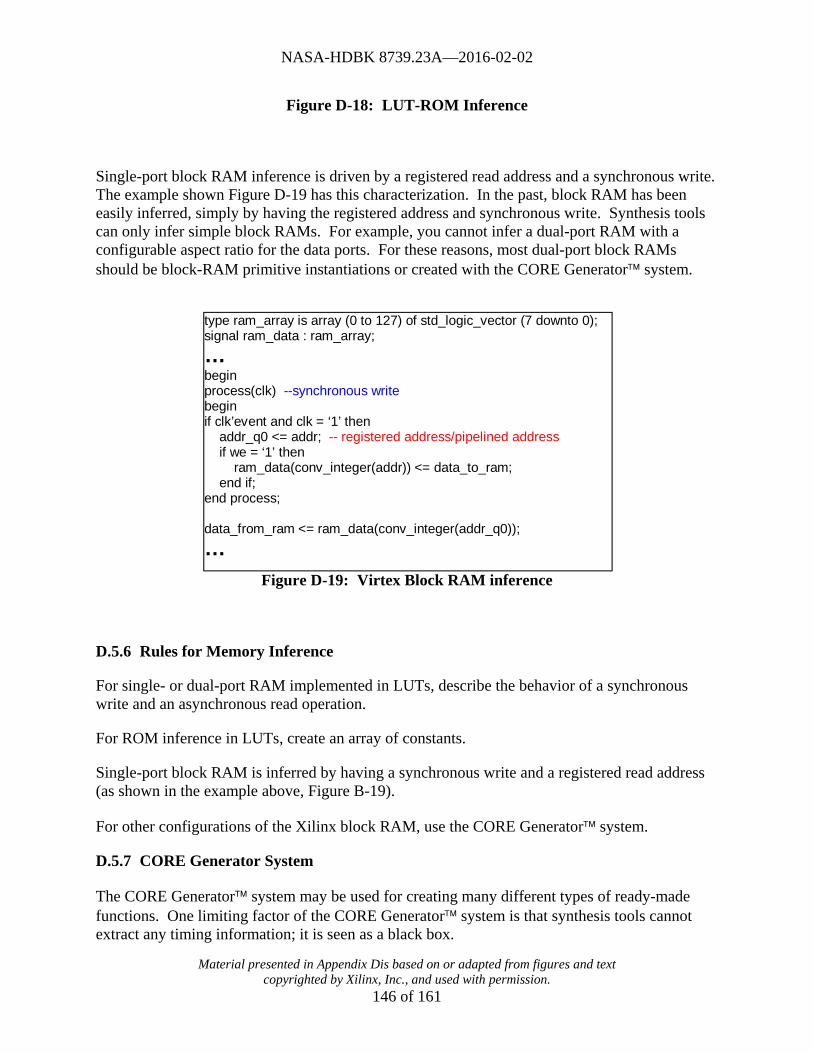
NASA-HDBK 8739.23A—2016-02-02
Material presented in Appendix Dis based on or adapted from figures and text copyrighted by Xilinx, Inc., and used with permission.
146 of 161
Figure D-18: LUT-ROM Inference
Single-port block RAM inference is driven by a registered read address and a synchronous write. The example shown Figure D-19 has this characterization. In the past, block RAM has been easily inferred, simply by having the registered address and synchronous write. Synthesis tools can only infer simple block RAMs. For example, you cannot infer a dual-port RAM with a configurable aspect ratio for the data ports. For these reasons, most dual-port block RAMs should be block-RAM primitive instantiations or created with the CORE Generator system.
Figure D-19: Virtex Block RAM inference
D.5.6 Rules for Memory Inference
For single- or dual-port RAM implemented in LUTs, describe the behavior of a synchronous write and an asynchronous read operation.
For ROM inference in LUTs, create an array of constants.
Single-port block RAM is inferred by having a synchronous write and a registered read address (as shown in the example above, Figure B-19).
For other configurations of the Xilinx block RAM, use the CORE Generator system.
D.5.7 CORE Generator System
The CORE Generator system may be used for creating many different types of ready-made functions. One limiting factor of the CORE Generator system is that synthesis tools cannot extract any timing information; it is seen as a black box.
type ram_array is array (0 to 127) of std_logic_vector (7 downto 0); signal ram_data : ram_array;
… begin process(clk) --synchronous write begin if clk’event and clk = ‘1’ then addr_q0 <= addr; -- registered address/pipelined address if we = ‘1’ then ram_data(conv_integer(addr)) <= data_to_ram; end if; end process; data_from_ram <= ram_data(conv_integer(addr_q0));
…

NASA-HDBK 8739.23A—2016-02-02
Material presented in Appendix Dis based on or adapted from figures and text copyrighted by Xilinx, Inc., and used with permission.
147 of 161
The CORE Generator system provides three files for a module:
Implementation file, <module_name>.ngc.
Instantiation template, <module_name>.vho
Simulation wrapper, <module_name>.vhd
For behavioral and post-synthesis simulation, the simulation wrapper file will have to be used. To simulate a CORE Generator module, the necessary simulation packages must be compiled. More information on using this flow and generating the necessary files can be found in the CORE Generator tool under Help Online Documentation.
The CORE Generator system provides simulation models in the $Xilinx/vhdl/src/XilinxCoreLib directory. There is a strict order of analysis that must be followed, which can be found in the analyze_order file located in the specified directory. In addition, Xilinx provides a Perl script for a fast and easy analysis of different simulators. To compile the XilinxCoreLib models with ModelSim or VSS, use the following syntax at a command prompt:
xilinxperl.exe $Xilinx/vhdl/bin/nt/compile_mti_vhdl.pl coregen
xilinxperl.exe $Xilinx/vhdl/bin/nt/compile_vss_vhdl.pl coregen
Compare logic is frequently implemented poorly in FPGAs. Compare logic is inferred by the use of <, <=, >, and >= VHDL operators. For a Xilinx implementation, this logic is best implemented when described with and-or implementations. When possible, look for patterns in the data or address signals that can be used to implement a comparison with gates, rather than compare logic. If a critical path includes comparison logic, an implementation that would use and-or logic should be considered.
D.5.8 Rule for Comparator Implementation
If a critical path has comparator logic in it, then try to implement the comparison by using and-or gates.
D.5.9 Xilinx Clock Enables
Clock enables are easily inferred, either explicitly or implicitly. Clock enables are very useful for maintaining a synchronous design. They are highly preferable over the unwanted gated clock. However, not all technologies support clock enables directly. For those architectures that do not support clock enables as a direct input to the register, it will be implemented via a feedback path. This type of implementation is not a highly regarded implementation style. Not only does it add a feedback path to the register, it also uses more logic because FPGA architecture requires two extra inputs into the LUT driving the register.

NASA-HDBK 8739.23A—2016-02-02
Material presented in Appendix Dis based on or adapted from figures and text copyrighted by Xilinx, Inc., and used with permission.
148 of 161
The Xilinx architecture supports clock enables as a direct input to a register. This is highly advantageous for a Xilinx implementation. However, the designer must be certain that the logic required to create the clock enable does not infer large amounts of logic, making it a critical path.
In the example shown below (Figure D-20), there is an explicit inference of a clock enable and an implicit inference of clock enables. In the first section, a clock enable is via explicitly testing for a terminal count. In the second section of code, the clock enables are implied for the signals cs and state. The clock enable for cs is inferred by not making an assignment to cs in the state init. The clock enable for the signal state is inferred by not defining all possible branches for the if-then-else statement, highlighted in red. When the if-then-else condition is false, state must hold its current value. Clock enables are inferred for these conditions when they are in a clocked process. For a combinatorial process, it would infer latches.
Figure D-20: Clock Enable Inference
D.5.10 Rules for Clock Enable Inference
Clock enables can only be inferred in a clocked process.
process (clk) -- Explicit inference of a clock enable begin -- process if rising_edge(clk) then if tc = '1' then cnt <= cnt + ‘1’; end if; end if; end process;
process (clk, reset) -- Implicit inference of a clock enable begin -- process if reset = '1' then state <= (others => '0'); cs <= "00"; elsif rising_edge(clk) then case (state) is when init => -- inference of a clock enable for signal cs state <= load; when fetch => if (a = '1' and b = '1') then -- inference of a clock enable for signal state state <= init; end if; cs <= "11"; when others => null; end case; end if; end process;

NASA-HDBK 8739.23A—2016-02-02
Material presented in Appendix Dis based on or adapted from figures and text copyrighted by Xilinx, Inc., and used with permission.
149 of 161
Clock enables can be inferred explicitly by testing an enable signal. If the enable is true, the signal is updated. If enable is false, that signal will hold its current value.
Clock enables can be implicitly inferred two ways:
Not assigning to a signal in every branch of an if-then-else statement or case statement. Remember that latches will be inferred for this condition in a combinatorial process (see section 5, Inadvertent latch Inference).
Not defining all possible states or branches of an if-then-else or case statement.
Pipelining with SRL
In Xilinx FPGAs, there is an abundance of registers; there are two registers per slice. This is sufficient for most registered signals. However, there are times when multiple pipeline delays are required at the end of a path. When this is true, it is best to use the Xilinx SRL (Shift Register LUT). The SRL uses the LUT as a shiftable RAM to create the effect of a shift register. In Figure D-21an example of how to infer the SRL is shown. This will infer a shift register with 16 shifts (width = 4). Although this will infer registers for an ASIC, it will infer the SRL when you are targeting a Xilinx part. The behavior that is required to infer the SRL is highlighted in blue. The size could be made parameterizable by using constants to define the signal widths. It could also be made into a procedure with parameterized widths and sizes.
Figure D-21: Inference of Xilinx Shift Register LUT (SRL)
library ieee ;use ieee.std_logic_1164.all ;
entity srltest is port(clk, en : in std_logic ; din : in std_logic_vector(3 downto 0); dout : out std_logic_vector(3 downto 0)) ;end srltest ;
architecture rtl of srltest is type srl_16x4_array is array (15 downto 0) of std_logic_vector(3 downto 0); signal sreg : srl_16x4_array ;begin dout <= sreg(15) ; -- read from constant location srl_proc : process (clk, en) begin if rising_edge(clk) then
if (en = '1') then sreg <= sreg(14 downto 0) & din ; -- shift the data
-- Current Value sreg (15:1) sreg(0)-- Next Value sreg (14:0) din
end if; end if;

NASA-HDBK 8739.23A—2016-02-02
Material presented in Appendix Dis based on or adapted from figures and text copyrighted by Xilinx, Inc., and used with permission.
150 of 161
D.5.11 Rules for SRL Inference
No reset functionality may be used directly to the registers.
If a reset is required, the reset data must be supplied to the SRL until the pipeline is filled with reset data.
You may read from a constant location or from a dynamic address location. In Xilinx Virtex-II parts, you may read from two different locations: a fixed location and a dynamically addressable location.
D.5.12 Technology-Specific Logic Generation – Generate Statements
This section has outlined ways that Xilinx-specific coding will differ from other solutions. Because many styles may exist for a similar block of code (for example a multiplexer), to get the optimal implementation, use VHDL generate statements. This is the best solution for a couple of reasons. Although configuration statements are commonly used to guide the synthesis of multiple implementation styles, some synthesis tools currently do not fully support them. Also, with generate statements, a change to a single constant will change the type of logic generated (ASIC or FPGA).
An example of using generate statements was covered in Figure D-12.
D.6 Coding for Synthesis
The main synthesis issues involve coding for minimum logic level implementation (i.e., coding for speed, max frequency); inadvertent logic inference; and fast, reliable, and reusable code.
D.6.1 Synchronous Design
The number one reason that a design does not work in a Xilinx FPGA is that the design uses asynchronous techniques. To clarify, the primary concern is asynchronous techniques used to insert delays to align data, not crossing clock domains. Crossing clock domains is often unavoidable, and there are good techniques for accomplishing that task via FIFOs. There are no good techniques to implement an asynchronous design. First, and most important, the actual delay can vary based on the junction temperature. Second, for timing simulations, Xilinx provides only maximum delays. If a design works based on the maximum delays, this does not mean that it will work with actual delays. Third, Xilinx will stamp surplus –6 (faster) parts with a –5 or –4 (slower speed) speed-grade. However, if the design is done synchronously there will be no adverse effects.
D.6.2 Clocking
In a synchronous design, only one clock and one edge of the clock should be used. There are exceptions to this rule. For example, by utilizing the 50/50 duty-cycle correction of the

NASA-HDBK 8739.23A—2016-02-02
Material presented in Appendix Dis based on or adapted from figures and text copyrighted by Xilinx, Inc., and used with permission.
151 of 161
DCM/DLL, in a Xilinx FPGA you may safely use both edges of the clock because the duty-cycle will not drift.
Do not generate internal clocks. Primarily, do not generate gated clocks because these clocks will glitch, propagating erroneous data. The other primary problems with internally generated clocks are clock-skew related problems. Internal clocks that are not placed on a global clock buffer will incur clock skew, making it unreliable. Replace these internally generated clocks with either a clock enable signal or generate divided, multiplied, phase shifted, etc. clocks with a clock generated via the DCM/DLL.
D.6.3 Rules for Clock Signals
Use one clock signal and one edge.
Do not generate internal clock signals because of glitching and clock-skew related problems.
D.6.4 Local Synchronous Sets and Resets
Local synchronous sets and resets eliminate the glitching associated with local asynchronous sets and resets. An example of such a problem is associated with the use of a binary counter that does not use the maximal binary count. For example, a four-bit binary counter has 16 possible binary counts. However, if the design calls only for 14 counts, the counter needs to be reset before it has reached its limit. An example of using local asynchronous resets is highlighted in red in Figure D-22. A well-behaved circuit is highlighted in blue, in the Figure D-23. For the binary counter that is using a local asynchronous reset, there will be glitching associated with the binary transitions, which will cause the local asynchronous reset to be generated. When this happens, the circuit will propagate erroneous data.

NASA-HDBK 8739.23A—2016-02-02
Material presented in Appendix Dis based on or adapted from figures and text copyrighted by Xilinx, Inc., and used with permission.
152 of 161
Figure D-22: Local Asynchronous Reset and TC & Well-Behaved Synchronous Reset & CE
Figure D-23: Well Behaved Local Asynchronous Reset and TC & Well-Behaved Synchronous Reset & CE
-- Asynchronous local reset and internally generated clockprocess (clk, reset, cnt_reset)begin -- process-- global and local async. reset if (reset = '1' or cnt_reset = '1') then
tc <= '0';cnt <= "0000";
elsif rising_edge(clk) thenif cnt = "1110" then cnt_reset <= '1'; tc <= '1';else cnt <= cnt + 1; tc <= '0'; cnt_reset <= '0';end if;
end if;end process;-- internally generated clock - tcprocess (tc, reset) begin -- process if reset = '1' then
data_en <= (others => '0'); elsif rising_edge(tc) then
data_en <= data; end if;
-- Synchronous Local reset and clock enable useprocess (clk, reset) variable tc : std_logic := '0';begin -- process if reset = '1' then -- global asynchronous reset
cnt <= "0000";data_en <= (others => '0');
elsif rising_edge(clk) then if cnt = "1110" then
cnt <= "0000"; -- local synchronous reset data_en <= data; -- terminal count clock enable
else cnt <= cnt + '1'; tc := '0';
end if; end if;end process;

NASA-HDBK 8739.23A—2016-02-02
Material presented in Appendix Dis based on or adapted from figures and text copyrighted by Xilinx, Inc., and used with permission.
153 of 161
D.6.5 Rule for Local Set or Reset Signals
A local reset or set signal should use a synchronous implementation.
Pipelining
Pipelining is the act of inserting registers into one path to align that data with the data in another path, such that both paths have an equal amount of latency. Pipelining may also decrease the amount of combinatorial delay between registers, thus increasing the maximum clock frequency. Pipelines are often inserted at the end of a path by using a shift register implementation. Shift registers in Xilinx’s Virtex parts are best implemented in the LUT as an SRL, as described in section D.4. Signal naming for pipelined signals is covered in section D.1.
Registering Leaf-Level Outputs and Top-Level Inputs
A very robust technique, used in synchronous design, is registering outputs of leaf-levels (sub-blocks). This has several advantages:
No optimization is needed across hierarchical boundaries.
Enables the ability to preserve the hierarchy.
Bottom-up compilation.
Recompile only those levels that have changed.
Enables hierarchical floorplanning.
Increases the capability of a guided implementation.
Forces the designer to keep like-logic together.
Similarly, registering the top-level inputs decreases the input to clock (ti2c) delays; therefore, it increases the chip-to-chip frequency.
D.6.6 Rules for the Hierarchical Registering of Signals
Register outputs of leaf-level blocks.
Register the inputs to the chip’s top-level.
D.6.7 Clock Enables
The use of clock enables increases the routability of a Xilinx implementation and maintains synchronous design. The use of clock enables is the correct alternative to gated clocks.
Clock enables increase the routability of the design because the registers with clock enables will run at a reduced clock frequency. If the clock enable is one-half the clock rate, the clock enabled datapaths are placed-and-routed once the full clock frequency paths have been placed-and-routed. The clock enable should have a timing constraint placed on it so that the Xilinx

NASA-HDBK 8739.23A—2016-02-02
Material presented in Appendix Dis based on or adapted from figures and text copyrighted by Xilinx, Inc., and used with permission.
154 of 161
implementation tools will recognize the difference between the normal clock frequency and the clock-enabled frequency. This will place a lower priority on routing the clock-enabled paths.
Gated clocks will introduce glitching in a design, causing incorrect data to be propagated in the data stream. Therefore, gated clocks should be avoided.
Using signals generated by sequential logic as clocks is a common error. For example, you use a counter to count through a specific number of clock cycles, producing a registered terminal count. The terminal count is then used as a clock to register data. This internal clock is routed on the general interconnect. The skew on internally generated clocks can be so detrimental that it causes errors. This may also cause race conditions if the data is resynchronized with the system clock. This error is illustrated in Figure D-23. The text highlighted in red is the implementation using the terminal count as a clock.
Instead, generate the terminal count one count previous, and use the terminal count as a clock enable for the data register. The text highlighted in blue is the well-behaved implementation using the terminal count as a clock enable. An explanation of the reset signals is covered section D.6.5.
It may be useful to generate clock enables by using a state machine. The state machine can be encoded at run time by the synthesis tool. Thus a one-hot, gray, or Johnson encoding style could be used. It is also possible to produce precisely placed clock enables by using a linear feedback shift register (LFSR), also known as a pseudo-random bitstream generator (PRBS generator). Xilinx provides application notes on the use of LFSRs.
Clock enables for Xilinx implementations are further discussed in section 4.
D.6.8 Rules for Clock Enable
Use clock enables in place of gated clocks.
Use clock enables in place of internally generated clocks.
Finite State Machines
Coding for Finite State Machines (FSM) includes analyzing several tradeoffs.
D.6.9 Encoding Style
Enumerated types in VHDL allow the FSM to be encoded by the synthesis tool. However, the encoding style used will not be clearly defined in the code but rather in the synthesis tool. Therefore, good documentation should be provided -- stating specifically which encoding style was used. By default, most synthesis tools will use binary encoding for state machines with less than five states: one-hot for 5 to 24 states and gray for more than 24 states (or similar). Otherwise, synthesis will use one-hot encoding. One-hot encoding is the suggested implementation for Xilinx FPGAs because Xilinx FPGAs have abundant registers. Other encoding styles may also be used -- specifically gray encoding. For a gray-encoding style, only one-bit transitions on any given state transition (in most cases); therefore, less registers are used

NASA-HDBK 8739.23A—2016-02-02
Material presented in Appendix Dis based on or adapted from figures and text copyrighted by Xilinx, Inc., and used with permission.
155 of 161
than for a one-hot implementation, and glitching is minimized. The tradeoffs for these encoding styles can easily be analyzed by changing a synthesis FSM attribute and running it through synthesis to get an estimate of the timing. The timing shown in synthesis will most likely not match the actual implemented timing; however, the timing shown between the different encoding styles will be relative, therefore providing the designer a good estimate of which encoding style to use.
Another possibility is to specifically encode the state machine. This is easily done via the use of constants. The code will clearly document the encoding style used. In general, one-hot is the suggested method of encoding for FPGAs -- specifically for Xilinx. A one-hot encoding style uses more registers, but the decoding for each state (and the outputs) is minimized, increasing performance. Other possibilities include gray, Johnson (ring-counter), user-encoded, and binary. Again, the tradeoffs can easily be analyzed by changing the encoding style and synthesizing the code.
Regardless of the encoding style used, the designer should analyze illegal states. Specifically, are all the possible states used? Often, state machines do not use all the possible states. Therefore, the designer should consider what occurs when an illegal state is encountered. Certainly, a one-hot implementation does not cover all possible states. For a one-hot implementation, many illegal states exist. Thus, if the synthesis tool must decode these states, it may become much slower. The code can also specifically report what will happen when an illegal state is encountered by using a “when others” VHDL case statement. Under the “when others” statement, the state and all outputs should be assigned to a specific value. Generally, the best solution is to return to the reset state. The designer could also choose to ignore illegal states by encoding “don’t care” values (‘X’) and allow the synthesis tool to optimize the logic for illegal states. This will result in a fast state machine, but illegal states will not be covered.
D.6.10 Rules for Encoding FSMs
For enumerated-types, encode the state machine with synthesis-specific attributes. Decide if the logic should check for illegal states.
For user-encoded state machines, the designer should analyze whether the logic should check for illegal states or not, and the designer should accordingly write the “when others” statement. If the designer is concerned with illegal states, the state machine should revert to the reset state. If the designer is not concerned with illegal states, the outputs and state should be assigned "X" in the “when others” statement.
Xilinx suggests using one-hot encoding for most state machines. If the state machine is large, the designer should consider using a gray or Johnson encoding style and accordingly analyze the tradeoffs.
D.6.11 FSM VHDL Processes
Most synthesis tools suggest coding state machines with three process statements: one for the next state decoding, one for the output decoding, and one for registering of outputs and state bits. This is not as concise as using one process statement to implement the entire state machine;

NASA-HDBK 8739.23A—2016-02-02
Material presented in Appendix Dis based on or adapted from figures and text copyrighted by Xilinx, Inc., and used with permission.
156 of 161
however, it allows the synthesis tools the ability to better optimize the logic for both the outputs and the next-state decoding. Another style is to use two processes to implement the state machine: one for next state and output decoding and the other process for registering of outputs and state bits.
The decision to use one, two, or three process statements is entirely left up to the discretion of the designer. Moore state machines (output is dependent only on the current state) generally have limited decoding for the outputs, and the state machine can, therefore, be safely coded with either one or two process statements. Mealy state machine (outputs depend on the inputs and the current state) output decoding is generally more complex, and, therefore, the designer should use three processes. Mealy state machines are also the preferred style for FSMs because it is advantageous to register the outputs of a sub-block (as described above in section 5). Mealy state machines will have the least amount of latency with registered outputs. Mealy state machines can be used with a look-ahead scheme. Based on the current state and the inputs, the outputs can be decoded for the next state. For simple state machines where the output is not dependent on the inputs, a Moore implementation is equivalent to a look-ahead scheme. That is, the outputs can be decoded for the next state and appropriately registered to reflect the next state (rather than reflecting the current state). The purpose of this scheme is to introduce the least amount of latency when registering the outputs.
D.6.12 Rules for FSM Style
Generally, use three process statements for a state machine: one process for next-state decoding, one for output decoding, and one for the registering of state bits and outputs.
Use a Mealy look-ahead state machine with registered outputs whenever possible, or use a Moore state machine with next-state output decoding and registered outputs to incur the minimum amount of latency.
D.6.13 Logic Level Reduction
To minimize the number of cascaded logic levels, we need to follow a few simple rules of coding.
D.6.14 If-Then-Else and Case Statements
If-then-else and case statements can cause unwanted effects in a design. Specifically, nested If-then-else and case statements may cause extra levels of logic inference. This occurs because if-then-else statements generally infer priority-encoded logic. However, one level of an if-then-else will not necessarily create priority-encoded logic. For that matter, synthesis tools generally handle if-then-else or case statements very well and create parallel logic rather than priority encoded logic.
Often, a nested if statement can be combined in the original if statement and result in a reduced amount of inferred logic. A simple example is shown in Figure D-24, which shows how priority encoded logic creates cascaded logic. Nested case statements can have the same effect, as can the combination of nested case and if-then-else statements.

NASA-HDBK 8739.23A—2016-02-02
Material presented in Appendix Dis based on or adapted from figures and text copyrighted by Xilinx, Inc., and used with permission.
157 of 161
Priority-encoded logic can be generated for other reasons. The use of overlapping conditions in if-then-else branches causes the generation of priority-encoded logic. This condition should be avoided. There are times that priority-encoded logic must be used and may be intended. If the selector expressions in the if-then-else statement branches are not related, then priority-encoded logic will be created. Although this may be the intent, its use should be cautioned.
Figure D-24: Priority Encoded Logic
D.6.15 Rules for If-Then-Else and Case Statements
Limit the use of nested if-then-else and case statements.
Avoid overlapping conditions in if-then-else statements – this condition will infer priority-encoded logic.
Avoid using mutually exclusive branch expressions if possible. This condition will always infer priority-encoded logic.
Instead, use mutually exclusive if-then statements for each expression (if possible).
D.6.16 For Loops
Similar to the use of if-then-else and case statements, "for loops" can create priority-encoded logic. While for loops can be a very powerful tool for creating logic, the designer should evaluate their effects.
A simple example of the adverse effect of for loops is shown in Figure D-25. Fortunately, this is a situation that most tools handle well, but in our goal of creating reusable (portable) code, this situation should be avoided.

NASA-HDBK 8739.23A—2016-02-02
Material presented in Appendix Dis based on or adapted from figures and text copyrighted by Xilinx, Inc., and used with permission.
158 of 161
Figure D-25: For-Loop Cascaded Logic Implementation
D.6.17 Rule for Loops
Be cautious of using for loops for creating logic. Evaluate the logic created by the synthesis tool. There will likely be another way to write the code to implement the same functionality with the logic implemented in parallel.
Inadvertent Latch Inference
Inadvertent latch inference is a common problem that is easily avoided. Latches are inferred for two primary reasons: one, not covering all possible branches in if-then-else statements and two, not assigning to each signal in each branch. This is only a problem in a combinatorial process. For a clocked process, registers with clock enables are synthesized (as covered in the Xilinx Specific Coding section, section B.4).
A latch inference example for each of these cases is shown in Figure D-26. For section one, each possible state was not covered. This is a very common mistake for one-hot encoded state machines. Section one is an example of Moore FSM output decoding. The latch inference would be eliminated by the use of a final "else" statement with an assignment in that branch to the signal "cs."
For the second section of code, the latches are inferred because each signal is not assign in each state.
In Figure D-27, the inference of latches is eliminated by covering all possible branches and assigning to each signal in each branch. The fixes are highlighted in blue. For the case implementation, the default assignment to cs before the case statement specifies a default assignment for each state. This way, each bit is changed depending on the state. This is equivalent to making a signal assignment in each branch. For the if-then-else statement, adding the else clause solves the problem.
process (data_vec) variable parity_v : std_logic;beginparity_v := ‘0’;for i in data_vec’range loop parity_v := parity_v xor data_vec(i);end loop;parity <= parity_v;end process;
parity
[0]
loop1_parity_v_4
[1]
loop2_parity_v_3
[2]
[3]
parity
data_vec[3:0] [3:0]

NASA-HDBK 8739.23A—2016-02-02
Material presented in Appendix Dis based on or adapted from figures and text copyrighted by Xilinx, Inc., and used with permission.
159 of 161
Figure D-26: Latch Inference
Figure D-27: Elimination of Inadvertent Latch Inference
D.6.18 Rules for Avoidance of Latch Inference
Cover all possible branches.
-- (1) Did not specify each possible stateprocess (state)beginif state = “001” then cs <= “01”;elsif state = “010” then cs <= “10”;elsif state = “100” then cs <= “11”;end if;end process;
-- (2) Did not specify all possible-- outputs for each stateprocess (state) begin case (state) is when "001" => cs(0) <= '1'; when "010" => cs(1) <= '1'; when "100" => cs(1 downto 0) <= "11"; when others => cs(1 downto 0) <= "00"; end case; end process;
latrs
cs_1[1]
0 D0 C [1]QR
S
latrs
cs_1[0]
0 D0 C [0]QR
S
un1_un2_state_2
0
1
[2]
un1_un2_state_1
0
1
[2]
un3_state
[0]
[1]
[2]un1_un2_state
[1]
[0]
un2_state_2
[0]
[1]
un2_state_1
[1]
[0]
un1_state
[0]
[1]
[2]
cs[1:0][1:0]
state[2:0] [2:0]
-- (1) Fixed Case implementation (2) Fixed if-then-else implementationprocess (state) process (state) begin begin cs <= "00"; if state = "001" then case (state) is cs <= "01"; when "001" => elsif state = "010" then cs(0) <= '1'; cs <= "10"; when "010" => elsif state = "100" then cs(1) <= '1'; cs <= "11"; when "100" => else cs <= "11"; cs <= "00"; when others => end if; cs <= "00"; end process; end case; end process;

NASA-HDBK 8739.23A—2016-02-02
Material presented in Appendix Dis based on or adapted from figures and text copyrighted by Xilinx, Inc., and used with permission.
160 of 161
Assign to all signals at all branches.
APPENDIX E PLD ASSESSMENT FORM
The following form will be completed during the initial evaluation of the PLDs function and at each major milestone as need dictates. This completed for will become a perment part of the Configuration Management records of the project with a copy being stored by Quality Assurance.

NASA-HDBK 8739.23A—2016-02-02
Material presented in Appendix Dis based on or adapted from figures and text copyrighted by Xilinx, Inc., and used with permission.
161 of 161
PLD Quality Assurance Assessment Report Project Name: Date: Project Manager: Quality Assurance Engineer: The following section determines if the PLD is safety critical. If any of the criteria is yes the PLD is safety critical.
Criteria Evaluation
Yes No Comments The PLD controls a hazard
The PLD monitors a hazard
The PLD can cause or contribute to a hazard
The PLD is used to mitigate a hazard
Provides data needed to make a safety critical decision
The PLD is used to verify or validate safety-critical systems
The following section determines if the PLD is mission critical. If any of the criteria is yes the PLD is mission critical.
Criteria Evaluation
Yes No Comments If the PLD failed would loss of mission or mission failure occur?
If the PLD failed, would test objectives or facilities be impacted?
The PLD classification is determined using Appendix C in NASA-HDBK-4008. A classification factor of 1 through 5 is determined.
PLD Classification Comment
The PLD QA level of effort is determined using GLPR 7120.5.30 section 11.1.
Quality Assurance Effort Low
(Class 1 or 2) Medium (Class 3)
High (Class 4 or 5)
Comment
______________________________________ _____________________________________ QA Engineer Date ProjectManager Date