NANOSTRUCTURED FUNCTIONAL CERAMIC COATINGS · PDF fileNanostructured functional ceramic...
8
© 2007 Advanced Study Center Co. Ltd. Rev.Adv.Mater.Sci. 15(2007) 16-23 Corresponding author: Sanjay Mathur, e-mail: [email protected] NANOSTRUCTURED FUNCTIONAL CERAMIC COATINGS BY MOLECULE-BASED CHEMICAL VAPOR DEPOSITION Sanjay Mathur 1,2 , Hao Shen 1 and Jessica Altmayer 1 1 Leibniz Institute of New Materials, Saarbruecken, Germany 2 Department of Chemistry, Wuerzburg University, Wuerzburg, Germany Received: January 22, 2007 Abstract. Thin film deposition by chemical vapor deposition (CVD) techniques plays a dominant role in the development of both protective and functional coatings, important for their technological implications. Commonly, multi-component materials are prepared from a mixture of precursors, however the efficiency of such processes is hampered by the mis-match of chemical reactivity such as differential thermal stability and vapor pressure of individual precursor species. Conse- quently, phase separation and elemental segregation are usually observed in coatings produced by CVD. De-mixing of elements in multi-component systems is thermodynamically driven and sensitive to the chemical behavior of the precursors. Transformation of precursor compounds possessing bonding features inherent to the solid-state lowers the need of diffusion and counter- balances the thermodynamic impediments. We discuss here the role of pre-defined chemical precursors in reducing the constraints imposed on conventional CVD techniques, which require rather high deposition temperatures and generally offer marginal control over microstructure and surface topography. Examples dealing with the decomposition of molecular sources in CVD pro- cess to deposit gas sensing, photocatalytic and bio-compatible coatings are also presented. 1. INTRODUCTION Development of nanostructured ceramic coatings has become an important research area mainly due to the interesting chemical and physical properties of nanoscaled materials [1-11]. Chemical vapor deposition (CVD) is a versatile technique for low- temperature deposition of functional ceramics with attractive process features such as up-scaling to large scale production, conformal coverage, and easy regulation of deposition parameters. In mol- ecule-based CVD techniques, the deposition pro- cess operate at atomic or molecular level, which opens up the possibility of obtaining dense micro- structure and thus allow to achive the beneficial properties of monolithic ceramics (high thermal, mechanical and chemical resistance) in form of pro- tective and functional coatings. In addition, appli- cation of well-defined molecules as precursor units offers precise control over structure, morphology and composition of resulting coatings either through influence of chemical design or by the variation of process parameters [12-14]. The molecule-to-material concept denotes the transformation of the intrinsic chemical configura- tion of molecular precursors, under non-equilibrium conditions, into solid phases at much lower tem- peratures than those required for conventional ce- ramic processing procedures [12]. One of the ba- sic requirements for thin film growth is that the pre- cursor units adsorb on the substrate only at spe-
-
Upload
hoangkhanh -
Category
Documents
-
view
220 -
download
4
Transcript of NANOSTRUCTURED FUNCTIONAL CERAMIC COATINGS · PDF fileNanostructured functional ceramic...
16 Sanjay Mathur, Hao Shen and Jessica Altmayer
© 2007 Advanced Study Center Co. Ltd.
Rev.Adv.Mater.Sci. 15(2007) 16-23
Corresponding author: Sanjay Mathur, e-mail: [email protected]
NANOSTRUCTURED FUNCTIONAL CERAMIC COATINGSBY MOLECULE-BASED CHEMICAL VAPOR DEPOSITION
Sanjay Mathur1,2, Hao Shen1 and Jessica Altmayer1
1Leibniz Institute of New Materials, Saarbruecken, Germany2Department of Chemistry, Wuerzburg University, Wuerzburg, Germany
Received: January 22, 2007
Abstract. Thin film deposition by chemical vapor deposition (CVD) techniques plays a dominantrole in the development of both protective and functional coatings, important for their technologicalimplications. Commonly, multi-component materials are prepared from a mixture of precursors,however the efficiency of such processes is hampered by the mis-match of chemical reactivitysuch as differential thermal stability and vapor pressure of individual precursor species. Conse-quently, phase separation and elemental segregation are usually observed in coatings producedby CVD. De-mixing of elements in multi-component systems is thermodynamically driven andsensitive to the chemical behavior of the precursors. Transformation of precursor compoundspossessing bonding features inherent to the solid-state lowers the need of diffusion and counter-balances the thermodynamic impediments. We discuss here the role of pre-defined chemicalprecursors in reducing the constraints imposed on conventional CVD techniques, which requirerather high deposition temperatures and generally offer marginal control over microstructure andsurface topography. Examples dealing with the decomposition of molecular sources in CVD pro-cess to deposit gas sensing, photocatalytic and bio-compatible coatings are also presented.
1. INTRODUCTIONDevelopment of nanostructured ceramic coatingshas become an important research area mainly dueto the interesting chemical and physical propertiesof nanoscaled materials [1-11]. Chemical vapordeposition (CVD) is a versatile technique for low-temperature deposition of functional ceramics withattractive process features such as up-scaling tolarge scale production, conformal coverage, andeasy regulation of deposition parameters. In mol-ecule-based CVD techniques, the deposition pro-cess operate at atomic or molecular level, whichopens up the possibility of obtaining dense micro-structure and thus allow to achive the beneficialproperties of monolithic ceramics (high thermal,
mechanical and chemical resistance) in form of pro-tective and functional coatings. In addition, appli-cation of well-defined molecules as precursor unitsoffers precise control over structure, morphologyand composition of resulting coatings either throughinfluence of chemical design or by the variation ofprocess parameters [12-14].
The molecule-to-material concept denotes thetransformation of the intrinsic chemical configura-tion of molecular precursors, under non-equilibriumconditions, into solid phases at much lower tem-peratures than those required for conventional ce-ramic processing procedures [12]. One of the ba-sic requirements for thin film growth is that the pre-cursor units adsorb on the substrate only at spe-
17Nanostructured functional ceramic coatings by molecule-based chemical...
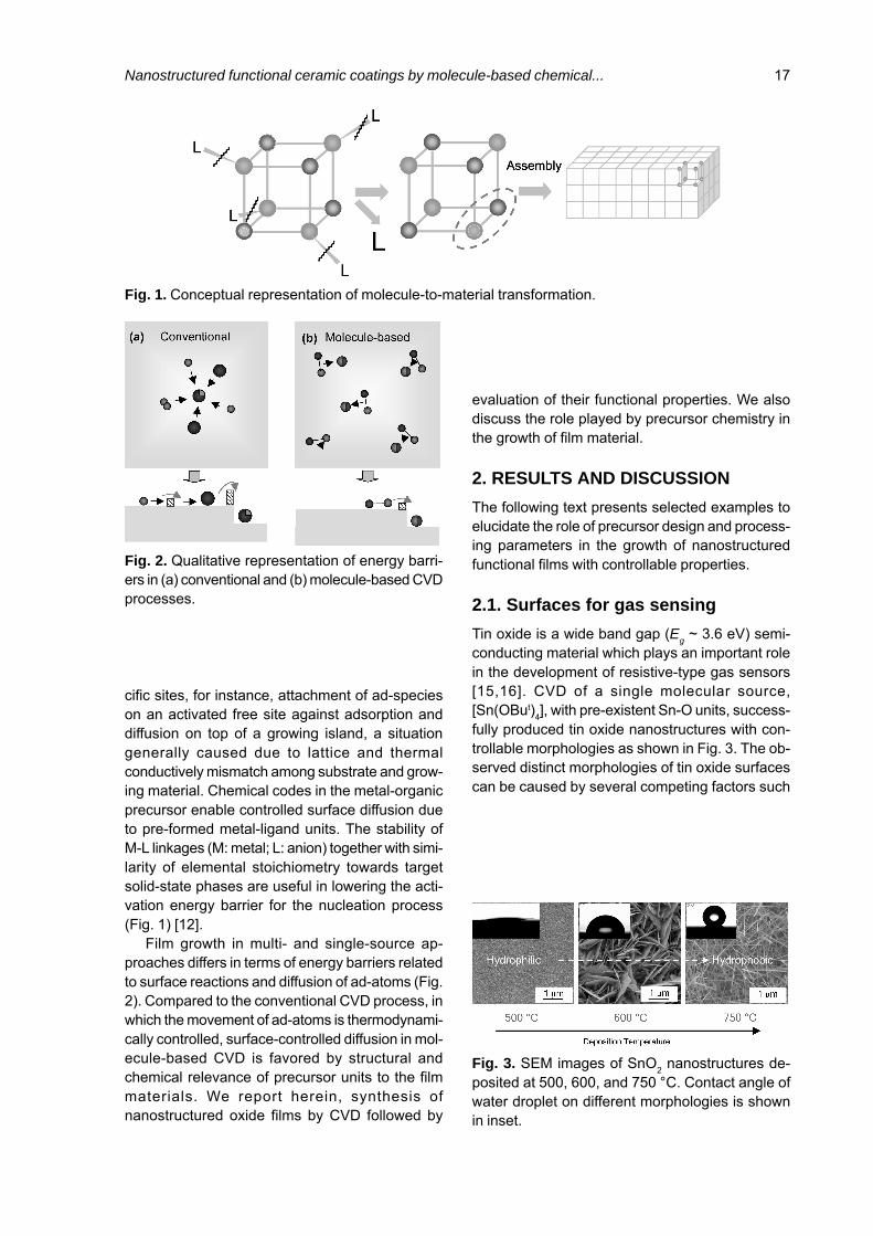
Fig. 1. Conceptual representation of molecule-to-material transformation.
cific sites, for instance, attachment of ad-specieson an activated free site against adsorption anddiffusion on top of a growing island, a situationgenerally caused due to lattice and thermalconductively mismatch among substrate and grow-ing material. Chemical codes in the metal-organicprecursor enable controlled surface diffusion dueto pre-formed metal-ligand units. The stability ofM-L linkages (M: metal; L: anion) together with simi-larity of elemental stoichiometry towards targetsolid-state phases are useful in lowering the acti-vation energy barrier for the nucleation process(Fig. 1) [12].
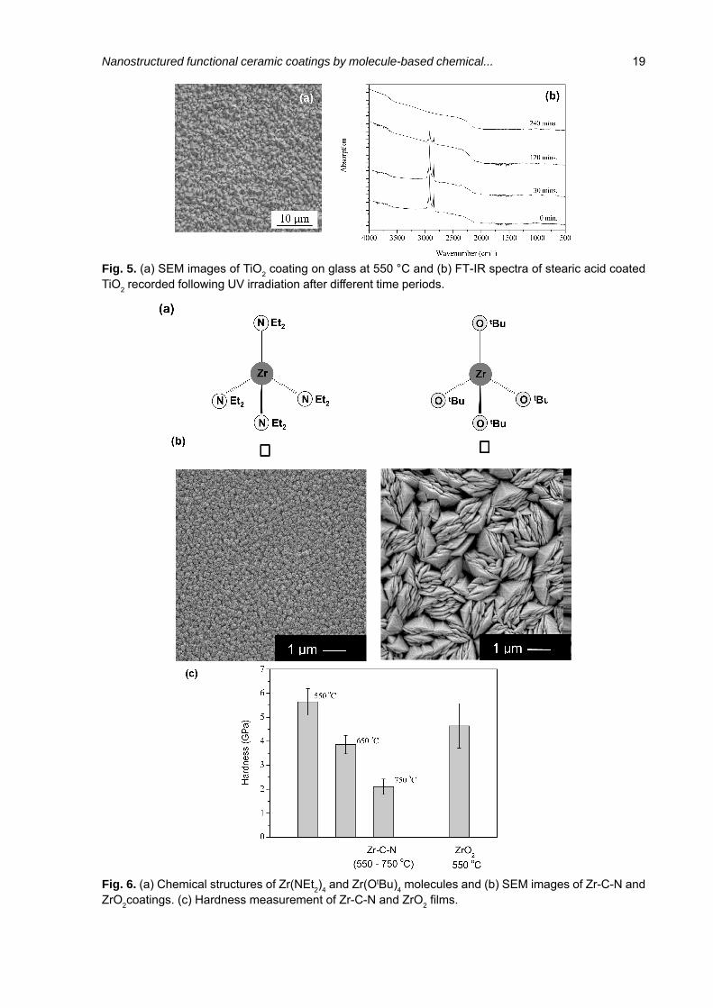
Film growth in multi- and single-source ap-proaches differs in terms of energy barriers relatedto surface reactions and diffusion of ad-atoms (Fig.2). Compared to the conventional CVD process, inwhich the movement of ad-atoms is thermodynami-cally controlled, surface-controlled diffusion in mol-ecule-based CVD is favored by structural andchemical relevance of precursor units to the filmmaterials. We report herein, synthesis ofnanostructured oxide films by CVD followed by
evaluation of their functional properties. We alsodiscuss the role played by precursor chemistry inthe growth of film material.
2. RESULTS AND DISCUSSIONThe following text presents selected examples toelucidate the role of precursor design and process-ing parameters in the growth of nanostructuredfunctional films with controllable properties.
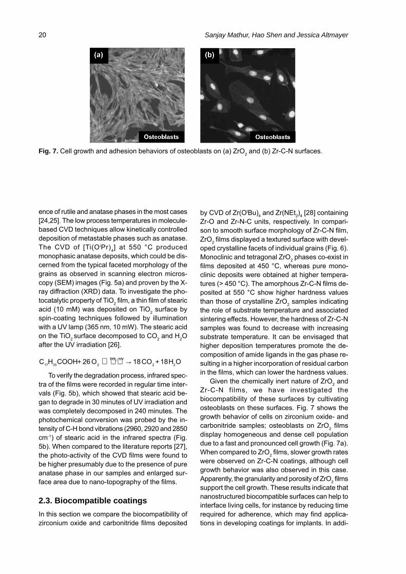
2.1. Surfaces for gas sensingTin oxide is a wide band gap (Eg ~ 3.6 eV) semi-conducting material which plays an important rolein the development of resistive-type gas sensors[15,16]. CVD of a single molecular source,[Sn(OBut)4], with pre-existent Sn-O units, success-fully produced tin oxide nanostructures with con-trollable morphologies as shown in Fig. 3. The ob-served distinct morphologies of tin oxide surfacescan be caused by several competing factors such
Fig. 3. SEM images of SnO2 nanostructures de-posited at 500, 600, and 750 °C. Contact angle ofwater droplet on different morphologies is shownin inset.
Fig. 2. Qualitative representation of energy barri-ers in (a) conventional and (b) molecule-based CVDprocesses.

18 Sanjay Mathur, Hao Shen and Jessica Altmayer
Fig. 4. (a) Gas sensing behaviors of SnO2 nanoparticles and nanowires and (b-c) the correspondingsensing mechanisms.
as sticking coefficient, surface diffusion, and en-ergy/flux distribution of the intermediate speciesand their interaction with the substrate, which allplay a role in the evolution of surface roughness.The films were deposited under similar precursorflux with substrate maintained at different tempera-tures. Films deposited at 500 °C showed a granu-lar morphology constituted by nano-sized particlesof regular shape, which can be attributed to an is-land-type growth due to film-substrate mismatchand the low mobility of grain boundaries at growthtemperatures. Upon increasing the temperature,development of texture effects was observed (Fig.3) probably due to the difference in the growth ratesbetween several crystal planes at the surface ofthe film [17]. Crystallites oriented with their slowergrowing direction normal to the surface are termi-nated while faster growing directions are preservedas they intersect the grain boundary. As a result,the obtained films are strongly faceted, generallyexhibiting faces corresponding to low index crys-tallographic planes. The growth rate of the differ-ent facets may depend on several factors, includ-ing their inclination relative to the precursor flux,sticking coefficients, site specific reaction rates, etc.This mechanism leads to preferential deposition/growth of atoms at low-energy surfaces in order tominimise the surface energy as revealed in thegrowth of one-dimensional nanostructures (Fig. 3).These results are interesting because microstruc-
ture and surface topography are critical parametersfor the performance of metal-oxide gas sensors[18]. Whereas smaller grain size can produce highsurface-to-volume ratios which can enhance sen-sitivity, one or two-dimensional single crystal filmshave the advantage of faster response as the ef-fects of grain boundary diffusion of the detectedgas and losses due to charge carrier scattering arereduced. Controlled modulation of surface micro-structure is desirable to be able to control the gassensing properties of ceramic coatings. Compara-tive evaluation of the gas sensitivity of films com-posed of nano-grains and nanowires towards car-bon monoxide (CO) revealed an enhanced gassensing performance (Fig. 4) for nanowire sample.The higher sensitivity is possibly due to increasedand selective adsorption of CO molecules on thecrystalline facets of nanowire structures, highercharge penetration and reduced charge percola-tion effects expected in a one dimentional struc-tures, when compared to granular film [19-21].
2.2. Photocatalytic coatingsAnatase and rutile modifications of titanium diox-ide (TiO2) exhibit different photo-chemical behav-ior due to different bandgap values (anatase: 3.18eV → rutile: 3.03 eV) [22,23]. Given the facile ana-tase to rutile phase transition, films processed byconventional processing techniques show coexist-
19Nanostructured functional ceramic coatings by molecule-based chemical...
Fig. 5. (a) SEM images of TiO2 coating on glass at 550 °C and (b) FT-IR spectra of stearic acid coatedTiO2 recorded following UV irradiation after different time periods.
Fig. 6. (a) Chemical structures of Zr(NEt2)4 and Zr(OtBu)4 molecules and (b) SEM images of Zr-C-N andZrO2coatings. (c) Hardness measurement of Zr-C-N and ZrO2 films.
⇓⇓⇓⇓⇓ ⇓⇓⇓⇓⇓
20 Sanjay Mathur, Hao Shen and Jessica Altmayer
ence of rutile and anatase phases in the most cases[24,25]. The low process temperatures in molecule-based CVD techniques allow kinetically controlleddeposition of metastable phases such as anatase.The CVD of [Ti(OiPr)4] at 550 °C producedmonophasic anatase deposits, which could be dis-cerned from the typical faceted morphology of thegrains as observed in scanning electron micros-copy (SEM) images (Fig. 5a) and proven by the X-ray diffraction (XRD) data. To investigate the pho-tocatalytic property of TiO2 film, a thin film of stearicacid (10 mM) was deposited on TiO2 surface byspin-coating techniques followed by illuminationwith a UV lamp (365 nm, 10 mW). The stearic acidon the TiO2 surface decomposed to CO2 and H2Oafter the UV irradiation [26].
C H COOH 26 O 18CO 18H O17 35 2
TiO , UV
2 22+ + →
To verify the degradation process, infrared spec-tra of the films were recorded in regular time inter-vals (Fig. 5b), which showed that stearic acid be-gan to degrade in 30 minutes of UV irradiation andwas completely decomposed in 240 minutes. Thephotochemical conversion was probed by the in-tensity of C-H bond vibrations (2960, 2920 and 2850cm-1) of stearic acid in the infrared spectra (Fig.5b). When compared to the literature reports [27],the photo-activity of the CVD films were found tobe higher presumably due to the presence of pureanatase phase in our samples and enlarged sur-face area due to nano-topography of the films.
2.3. Biocompatible coatingsIn this section we compare the biocompatibility ofzirconium oxide and carbonitride films deposited
Fig. 7. Cell growth and adhesion behaviors of osteoblasts on (a) ZrO2 and (b) Zr-C-N surfaces.
by CVD of Zr(OtBu)4 and Zr(NEt2)4 [28] containingZr-O and Zr-N-C units, respectively. In compari-son to smooth surface morphology of Zr-C-N film,ZrO2 films displayed a textured surface with devel-oped crystalline facets of individual grains (Fig. 6).Monoclinic and tetragonal ZrO2 phases co-exist infilms deposited at 450 °C, whereas pure mono-clinic deposits were obtained at higher tempera-tures (> 450 °C). The amorphous Zr-C-N films de-posited at 550 °C show higher hardness valuesthan those of crystalline ZrO2 samples indicatingthe role of substrate temperature and associatedsintering effects. However, the hardness of Zr-C-Nsamples was found to decrease with increasingsubstrate temperature. It can be envisaged thathigher deposition temperatures promote the de-composition of amide ligands in the gas phase re-sulting in a higher incorporation of residual carbonin the films, which can lower the hardness values.
Given the chemically inert nature of ZrO2 andZr-C-N films, we have investigated thebiocompatibility of these surfaces by cultivatingosteoblasts on these surfaces. Fig. 7 shows thegrowth behavior of cells on zirconium oxide- andcarbonitride samples; osteoblasts on ZrO2 filmsdisplay homogeneous and dense cell populationdue to a fast and pronounced cell growth (Fig. 7a).When compared to ZrO2 films, slower growth rateswere observed on Zr-C-N coatings, although cellgrowth behavior was also observed in this case.Apparently, the granularity and porosity of ZrO2 filmssupport the cell growth. These results indicate thatnanostructured biocompatible surfaces can help tointerface living cells, for instance by reducing timerequired for adherence, which may find applica-tions in developing coatings for implants. In addi-
21Nanostructured functional ceramic coatings by molecule-based chemical...
Fig. 8. The influence of chemical codes of precursors in controlling the CVD process and the resultingfunctional properties of ceramic coatings.
tion, it opens possibilities for modulating fundamen-tal cell behaviors (proliferation, adhesion, migra-tion and differentiation) by tuning the physical sur-face features.
3. CONCLUSIONSCeramic coatings are essential to improve the per-formance and extend the lifetime of the device
parts. The potential and versatility of the conven-tional high temperature CVD process can be sub-stantially enhanced by applying precursor-designconcept, which not only reduces the processingtemperature but also offers better film-substrateadhesion and facile microstructure control. The gasphase decomposition of molecular sources withdefined metal-ligand bonding is an interesting al-ternative to conventional multi-source approaches

22 Sanjay Mathur, Hao Shen and Jessica Altmayer
because the composition, microstructure, surfaceproperties of films can be programmed by precur-sor design in the synthetic stage and further tunedduring the stage of CVD processing by adjustingthe deposition parameters. Fig. 8 shows the intrin-sic and extrinsic influences of molecular precur-sors on the fabrication of nanostructured coatingswith controlled structure, morphology and functionalproperties. Most of the solutions and applicationsindicated in Fig. 8 are a function of the inherentproperties of the bulk material and unique featuresarising due to nanoscopic grain sizes (quantum ef-fects, surface area and surface energy).
The nanoparticle-nanoflake-nanowire morphol-ogy transition of SnO2 is probably related to sur-face energy and different growth rates along dif-ferent crystal directions. The temperature depen-dent diffusion rate and length play a key role in thestructure reorganization in order to minimize thesurface energy. The surface properties of SnO2such as hydrophilic → hydrophobic transition candepend not only on the variation of morphology,but also on the induced changes of surface chem-istry such as presence of defects, internal strainsand modified surface structures. The surface ef-fect of nanostructured films can be also observedin the investigation of photocatalytic behavior ofanatase TiO2 nanostructures. The metastable ana-tase with nano-topography can be obtained by ki-netically suppressing the grain growth of rutilephase at low deposition temperatures thereforeenhancing the photocatalytic performance of TiO2films. Ceramic coatings with tunable and multifunc-tional properties can be achieved by optimizationof precursor design and processing parameters.For instance, zirconium oxide and carbonitride filmscan be easily deposited by variation of precursorconfigurations and heat-treatment resulting in bet-ter adhesion, mechanical hardness andbiocompatibility. The controlled formation of func-tional ceramic coatings promises applications inthe area of nanoelectronics, gas sensors,photocatalysts and bio-technologies.
ACKNOWLEDGEMENTSAuthors are thankful to the Saarland state and cen-tral government for providing the financial assis-tance. Thanks are due to the German ScienceFoundation (DFG) for supporting this work in theframe of the priority programme on nanomaterials- Sonderforschungsbereich 277 - operating at theSaarland University, Saarbruecken, Germany.
REFERENCES[1] J. H. Fendler, Nanoparticles and
Nanostructured Films (Wiley-Vch, Germany,1998).
[2] Handbook of Chemical Vapor Deposition:Principles, Technologies and Applications, ed.by H. O. Pierson (Noyes Publications, NewJersey, 1992).
[3] Nanostructured Films and Coatings, NATOASI Series, 3, Vol. 78, ed. by G. M. Chow,J. A. Ovid’ko and T. Tsakalakos (KluwerAcademic Publishers, 2000).
[4] Y. Pauleau // Vacuum 61 (2001) 175.[5] Y. Pauleau and E. Thiery // Surf. Coat.
Technol. 180 (2004) 313.[6] W. Gulbiński, S. Mathur, H. Shen, T. Suszko,
A. Gilewicz and B. Warcholiński // Appl. Surf.Sci. 239 (2005) 302.
[7] S. Mathur, V. Sivakov, H. Shen, S. Barth,A. Nilsson and P. Kuhn // Thin Solid Films 502(2006) 88.
[8] S. Mathur, M. Veith, T. Ruegamer, E. Hemmerand H. Shen // Chem. Mater. 16 (2004) 1304.
[9] S. Mathur, S. Barth, H. Shen, J. C. Pyun andU. Werner // Small 1 (2005) 713.
[10] S. Mathur, H. Shen, V. Sivakov andU. Werner // Chem. Mater. 16 (2004) 2449.
[11] S. Mathur and P. Kuhn // Surf. Coat. Technol.(2006), 201 (2006) 807.
[12] S. Mathur and H. Shen, Encyclopedia ofNanoscience and Nanotechnology, Vol. 4 (H.S. Nalwa, American Scientific Publisher,2004) p.131.
[13] S. Mathur, M. Veith, V. Sivakov, H. Shen,V. Huch, U. Hartmann and H. B. Gao //Chem. Vap. Dep. 8 (2002) 277.
[14] W. S. Rees Jr., CVD of Nonmetals (Wiley,1996).
[15] P. G. Harrison and M. J. Willet // Nature 332(1988) 337.
[16] S. Ferrere, A. Zaban and B. A. Gregg //J. Phys. Chem. 101 (1997) 4490.
[17] A. van der Drift // Philips Res. Rep. 22(1967) 267.
[18] V. E. Henrich and P. A. Cox, The SurfaceScience of Metal Oxides (CambridgeUniversity Press, Cambridge, 1994).
[19] H. Huang, O. K. Tan, Y. C. Lee, T. D. Tran,M. S. Tse and X. Yao // Appl. Phys. Lett. 87(2005) 163123.
[20] Y. L. Wang, X. C. Jiang and Y. N. Xia //J. Am. Chem. Soc. 125 (2003) 16176.
23Nanostructured functional ceramic coatings by molecule-based chemical...
[21] A. Kolmakov, Y. X. Zhang, G. S. Cheng andM. Moskovits // Adv. Mater. 15 (2003) 997.
[22] P. J. Martin // J. Mater. Sci. 21 (1986) 1.[23] P. Lobl, M. Huppertz and D. Mergel // Thin
Solid Films 251 (1994) 72.[24] C. Legrand-Buscema, C. Malibert and
S. Bach // Thin Solid Films 418 (2002) 79.[25] M. C. Barnes, A. R. Gerson, S. Kumar and
N. Hwang // Thin Solid Films 446 (2004) 29.
[26] T. Minabe, D.A. Tryk, P. Sawunyama,Y. Kikuchi, K. Hashimoto and A. Fujishima //J. Photochem. Photobiol. A 137 (2000) 53.
[27] P. Sawunyama, A. Fujishima andK. Hashimoto // Langmuir 15 (1999) 3551.
[28] S. Mathur, J. Altmayer and H. Shen //Z. Anorg. Allg. Chem. 630 (2004) 2042.


![Nano Crystalline Ceramic and Ceramic Coatings …ceramic coatings could also provide improved properties for variety of applications, including wear resistant [9, 10] and thermal barrier](https://static.fdocuments.us/doc/165x107/5fe2e8e4f5c1aa72cd6c774b/nano-crystalline-ceramic-and-ceramic-coatings-ceramic-coatings-could-also-provide.jpg)