Nanostructured carbon/silicon composite opto ...Nanostructured carbon/silicon composite...
103
POLITECNICO DI TORINO SCUOLA INTERPOLITECNICA DI DOTTORATO Doctoral Program in Electronic Devices Final Dissertation Nanostructured carbon/silicon composite opto-electrochemical devices for sensing and energy harvesting applications Dario Imbraguglio Tutor Co-ordinator of the Research Doctorate Course prof. Fabrizio Candido Pirri prof. Giovanni Ghione 28/02/2013
Transcript of Nanostructured carbon/silicon composite opto ...Nanostructured carbon/silicon composite...
POLITECNICO DI TORINO
SCUOLA INTERPOLITECNICA DI DOTTORATO
Doctoral Program in Electronic Devices
Final Dissertation
Nanostructured carbon/silicon
composite opto-electrochemical devices
for sensing and energy harvesting
applications
Dario Imbraguglio
Tutor Co-ordinator of the Research Doctorate Course
prof. Fabrizio Candido Pirri prof. Giovanni Ghione
28/02/2013

2
3
POLITECNICO DI TORINO
NANOTECHNOLOGIES AND NANOSTRUCTURED
INNOVATIVE MATERIALS
Doctoral Program in Electronic Devices
Final Dissertation
Nanostructured carbon/silicon
composite opto-electrochemical devices
for sensing and energy harvesting
applications
Dario Imbraguglio

4
to my late mother
5
Contents
Preface ......................................................................................................................... 7
Abstract ....................................................................................................................... 9
1 Nanotechnologies and nanostructured innovative materials ....................... 11
1.1 Porous silicon ............................................................................................. 13
1.2 Porous silicon-based optical interferometric sensors ............................. 17
1.2.1 The Bruggeman’s effective medium approximation model ................ 17
1.2.2 Reflectometric interference Fourier transform spectroscopy (RIFTS) 18
1.2.3 Biosensing ............................................................................................ 22
1.3 Stabilization chemistries of porous silicon .............................................. 25
1.4 Nanostructured carbon/silicon hybrid devices ....................................... 29
1.4.1 Supercapacitors .................................................................................... 29
1.4.2 Next-generation high-capacity lithium ion batteries............................ 32
1.4.3 Porous silicon/carbon composite opto-electrochemical sensors .......... 35
2 Fabrication and characterization of porous silicon/carbon composite opto-
electrochemical sensors ........................................................................................... 38
2.1 From silicon to porous silicon .................................................................. 39
2.1.1 Four-point probe measurements of wafer resistivity ........................... 39
2.1.2 Electrochemical etching of crystalline silicon ..................................... 40
2.1.3 The spectroscopic liquid infiltration method (SLIM) .......................... 42
2.2 From porous silicon to carbonized porous silicon .................................. 45

6
2.2.1 The original carbonization procedure .................................................. 45
2.2.2 Ozone oxidation and furfuryl alcohol infiltration ................................ 46
2.2.3 Thermal polymerization and carbonization ......................................... 47
2.3 Porous silicon/carbon coupled opto-electrochemical sensors ............... 51
3 Experimental results ........................................................................................ 53
3.1 Tuning the carbon content and preliminary stability tests ................... 55
3.2 Electrochemical measurements of double-layer capacitances .............. 61
3.3 Coupled opto-electrochemical biosensing ............................................... 65
3.3.1 Positively charged biomolecules ......................................................... 67
3.3.2 Negatively charged biomolecules ........................................................ 72
Conclusions ............................................................................................................... 76
References ................................................................................................................. 77
Acknowledgements/Ringraziamenti ....................................................................... 86
PhD Publications and Awards ................................................................................ 88

7
Preface
The initial experimental activity of my PhD research project has been carried out at
the Istituto Nazionale di Ricerca Metrologica (INRIM) in Turin, Italy. Here, under
the supervision of Dr. Luca Boarino and Dr. Andrea Mario Rossi, I worked on two
main distinct topics:
Nanofabrication and characterization of silicon structures obtained by metal-
assisted chemical etching and nanospheres’ self-assembly;
Electron beam lithography on electrochemically etched porous silicon as
functionalization method for biotechnological applications.
So far, both efforts led to two publications on peer-reviewed journals, which are
listed below:
Boarino L, Imbraguglio D, Enrico E, De Leo N, Celegato F, Tiberto P, Pugno
N, Amato G: Fabrication of ordered silicon nanopillars and nanowires by
self-assembly and metal-assisted etching. Physica Status Solidi a-
Applications and Materials Science 2011, 208:1412-1416.
Imbraguglio D, Giovannozzi AM, Nastro A, Rossi AM: Submicron
machining and biomolecule immobilization on porous silicon by electron
beam. Nanoscale Research Letters 2012, 7:530.
The present thesis, instead, is entirely focused on recent studies conducted during the
final third year of my PhD at the University of California, San Diego (UCSD), under
the supervision of Professor Michael J. Sailor. The subjects of such a research were
also intended to be transferred to the silicon-based nanosystems concerned in the two
topics mentioned above, i.e. silicon nanowires and porous silicon, in order to
improve their physical-chemical properties and functionalization skills.

8
9
Abstract
My research activity deals with fabrication, characterization and functionalization
techniques of silicon-based nanostructures and systems, such as silicon nanowires
and nanostructured porous silicon. In particular, I focused my final dissertation thesis
on the synthesis and study of a new class of carbon/silicon nanocomposites,
produced by a recently discovered carbonization chemistry of porous silicon. Such a
new chemistry has been optimized in order to obtain samples amenable for
applications into a liquid dynamic environment. The employed carbon nanocasting
process provides both a stable and conductive hybrid nanomaterial, allowing the
carbonized porous silicon film to act as working electrode in aqueous media. The
electrode stability has been tried out in different liquids as well as under voltage
applied. Moreover, the optical properties of the nanostructure enable its use as a
sensor for electrically charged species in buffer solutions, such as biomolecular
complexes. By application of an electrical potential difference between the working
and a counter electrode, the sensor is able to simultaneously attract and detect both
positively than negatively charged targets. In the case of electroadsorbed
biomolecules, indications on the retention of their functional activity after releasing
from the electrode surface are also provided. Furthermore, an electrical measurement
system has been added to the optical one in order to monitor, in real-time with the
optically transduced signal, the current flowing between the two electrodes during
the sensing experiments. A few prototypes which synchronize the optical and
electrical responses of the sensor have been fabricated and their performances tested
by varying the electrical parameters. These new combined opto-electrochemical

10
devices can potentially find applications both in future label-free sensing than in
next-generation energy harvesting technologies.

11
1 Nanotechnologies and nanostructured
innovative materials
Nanotechnology is by now a very well-established and productive branch of applied
science to modern technological research. Nowadays, the achievement of technical
mastery in matter manipulation at the nanometer scale is regarded as the essential
requirement for the future development of new generation, advanced technological
devices. Over the years, such an acquired awareness has been particularly
consolidated by significant breakthroughs on the field of the so-called nanomaterials,
i.e., materials with special and distinguishing properties arising from morphological
features on an atomic or molecular scale.
Nanomaterials and nanostructures do not typically obey the same laws as
macroscopic systems and, on the other hand, they are not microscopic ones (i.e.,
single atoms or molecules). In such an intermediate (mesoscopic) dimensional range,
usually comprised between 2 nm and 50 or even 100 nm, quantum mechanical
effects become relevant, as well as functional for potentially revolutionary
applications like spintronics or quantum computing. In so far as more pressing
technological advances are today demanded, as in the renewable energy sector, the
other most important property of these systems can be exploited, that is the vastly
increased ratio of surface area to volume present in these materials. For instance, in
photovoltaics and power harvesting technologies, a high specific surface area is
oftentimes desirable in order to collect or store, respectively, an as much large
amount of energy as possible. Besides, the size of these structures is typically
12
comparable with that of biomolecules and other chemical compounds, thus further
extending applications to more interdisciplinary fields, like nanomedicine, sensing or
bioelectronics. To date, a flood of devices based on different nanostructures has been
proposed and realized for a variety of customized purposes, and a holistic approach
of research into materials has matured.
Silicon is still at present the element at the basis of modern consumer electronics, as
well as of 1st and 2
nd generation commercial solar cells. As a consequence, the
current interest on the onward and upward research into silicon-based nano structures
and materials is even higher. Depending on the use, different configurations of
nanostructured silicon, as in form of particles, wires or tubes, have been proposed
and realized. Among these, one of the most studied and versatile is known as porous
silicon (PS).

1.1 Porous silicon
PS can be thought as a silicon-based “sponge”, whose morphological features can be
tailored according to the specific function it has to fulfill (Figure 1-1). It is
commonly generated by electrochemical, stain or metal-assisted etching of
crystalline silicon in aqueous or non-aqueous electrolytes containing hydrofluoric
(HF) acid. In particular, if the electrochemical or the photoelectrochemical methods
are adopted, the size and shape of the pores, the porosity (i.e. the ratio between the
volume of voids and the total volume of PS), and its thickness can be easily
controlled by varying parameters such as the current density, the etching time, the
HF concentration, or the illumination intensity. Also depending on type and doping
level of the original silicon starting wafer, different kinds of porous structures can be
produced, covering an extensive range of pore sizes which spans from the macro- to
the microscale (< 2 nm).
Figure 1-1 Scanning electron microscope top (a) and cross-sectional (b) views of a PS sample.
After its official discovery in 1956, PS took a long time before arousing great
attention from the scientific community, which happened just in the early 1990s.
Before that time, the uses explored for PS were limited, for example, to the
14
fabrication of insulating [1] and metal [2] layers on silicon substrates or for vapor
sensing applications [3]. The turning point came with Leigh Canham, who first
observed efficient, multicolor, room temperature photoluminescence from the
material [4]. Almost simultaneously and independently, Ulrich Goesele and Volker
Lehmann reported their results about the widening of the PS energy band gap
because of quantum confinement effects [5].
Quantum confinement effects (e.g the Coulomb blockade [6]) take place in PS when
the diameters of the pores become large enough to extrude low dimensional silicon
crystallites. Bulk silicon itself is an indirect semiconductor with a relatively small
band gap energy of 1.1 eV (near-infrared). For this reason, bulk silicon does not
efficiently emit light and the photoluminescence is observed only at low temperature,
which makes unpractical its use in optoelectronic circuits and devices. III-V
semiconductors-based rather than silicon ones were considered for applications like
light-emitting diodes or semiconductor lasers, which require direct band gap
semiconductors in order to have an efficient generation of photons. Hence, the
findings of Canham, Goesele and Lehmann represented the possibility to expand
silicon technology from micro- to optoelectronics. Unfortunately, some stumbling
blocks related to the nature of the material (chemical and mechanical instability, low
electroluminescence efficiency, poor electrical transport) somewhat inhibited the
research in this field. PS, however, inspired research into a huge number of different
applications, and many devices based on PS, such as solar cells, photodetectors,
switches, displays, 1-D photonic crystals (“rugate filters”) or more complicated
photonic structures (Bragg reflectors, microcavities, optical gratings and
waveguides), have been proposed and demonstrated during the years.

15
Despite luminescence still remained one of the most important characteristics of PS
ever investigated, the present-day research on PS focus, instead, on other properties
of the material. For instance, in very recent years, the huge internal surface area
(which, in PS, can be widened from 10 up to even 1000 m2/cm
3) reawakened
enormous interest in energy harvesting technologies, since it can be potentially
harnessed to produce high-capacity lithium ion batteries (LIBs) of next-generation.
In addition, the tunable surface area of PS is reactive enough to allow for an
expanding repertoire of wet chemical functionalization techniques [7]. From the past,
a well-established modification chemistry has been developed to selectively bind
large amounts of different target analytes within the pores and, to date, just about any
surface termination can be achieved in PS upon demand. This, of course, has
important implications in sectors like the in vivo drug delivery, where two other
properties of PS turn out to be crucial, i.e. the biocompatibility and the
biodegradability. In this case, the use of PS as drug loading/delivery or imaging
material relies on its ability to degrade into harmless, biocompatible constituents. A
very active and promising research branch that has to be mentioned makes use, to
give an example, of PS micro and nano particles, which are able to host and locally
release drugs conceived for a specific disease [8].
Finally, the ability to control in a nanometric range the morphological features of PS,
such as the size of its pores, adds to the other characteristics of the material, and it
found large applications in sensing. A number of highly sensitive and selective both
chemical and biological sensors, all based on single- or multi-layered PS films,
emerged during the years. In particular, a novel class of PS-based optical
interferometric sensors derived from a very fruitful collaboration between the groups
of Sailor and Ghadiri [9, 10]. In the next section, the fundamental concepts of

16
interferometric sensing with PS optical films will be illustrated, since this is one of
the two (the main) transduction methods used by the opto-electrochemical devices
described in the present thesis.

1.2 Porous silicon-based optical interferometric
sensors
The working principle of an optical interferometric sensor based on PS rests on
monitoring characteristic changes in the refractive index of the porous matrix,
occurring when an analyte-containing or bare medium fills its pores.
1.2.1 The Bruggeman’s effective medium approximation
model
Being substantially a mixture of silicon and air, pristine PS is a two-phase composite,
and its refractive index is thus expected to be lower than that of bulk silicon.
Nevertheless, the direct determination of the refractive index (dielectric function) of
a PS layer is not an easy task, since it must take into account both the individual
constituents, i.e. the silicon skeleton and the medium filling the void spaces within
the pores (e.g. air), and the porosity of the film. Therefore, an “effective medium
approximation” must be used in order to estimate the optical constants of PS. Among
the existing theories, the Bruggeman’s model has been shown to predict porosity and
thickness of PS samples in good agreement with gravimetric determinations [10-12],
and it is one of the most used. An example of how the “effective” refractive index n
of a PS film can be calculated, by averaging the refractive indexes of the distinct
components in a Bruggeman’s picture, is given by the following relationship [10], in
the general case of any (gaseous or liquid) filling medium:
√
√
(
)

18
where nS is the wavelength-dependent refractive index of the silicon skeleton of the
porous matrix, nM is the wavelength-independent refractive index of the medium
filling the pores, and P is the porosity.
Figure 1-2 Reflected white light spectrum collected in air of a PS sample.
1.2.2 Reflectometric interference Fourier transform
spectroscopy (RIFTS)
Interferometric optical sensing with PS is obtained through the so-called RIFTS
(reflectometric interference Fourier transform spectroscopy) method [13-19]. Such a
technique takes advantage of the fact that illumination of sufficiently narrow-sized
porous samples causes multiple reflections of light at the interfaces of PS layers. In
the particular case of a single layer, the interfaces are just two: the upper one
between medium and PS and the lower one between PS and the underlying silicon
bulk. This phenomenon results into constructive and destructive interference effects
which lead to the formation of a regular interferometric optical pattern (Fabry-Pérot
fringes). For a PS-based sample to display Fabry-Pérot fringes, the layer must be flat
and reflective and the pores much smaller than the light wavelength (~500 nm),
otherwise incoherent light scattering will dominate the interference spectrum. Since
the PS samples intended for the present work are mesoporous (i.e. with a disordered

19
distribution of pore sizes comprised between 2 and 50 nm) single layers, they exhibit
an optical interferometric pattern like the one of Figure 1-2, which has been reported
as representative example.
The Figure 1-2 shows the raw reflected light spectrum in air, plotted in terms of
wavelengths, of an as-etched PS sample. The sample was illuminated with focused
white light, and reflected light was collected through the same lens positioned along
an axis normal to the PS surface and then transmitted to a CCD-based spectrometer.
The RIFTS method applies a fast Fourier transform (FFT) algorithm to the frequency
spectrum associated with the input waveform of Figure 1-2, enabling to extract the
basic optical parameters of the PS film. The raw spectra of Figure 1-2 were therefore
inverted in units of frequency in order for the Fabry-Pérot fringes to be periodic, the
data interpolated to be evenly spaced, and the resulting reflectance spectrum was
transformed by a digital FFT. This computation yields a peak whose position and
intensity is directly connected to the PS optical constants. An example of the FFT of
the reflectance spectrum of a single layer Fabry-Pérot PS film is reported in Figure 1-
3.
Figure 1-3 Corresponding Fourier transform of spectrum from Figure 1-2.
20
The peak in Figure 1-3 has been obtained from the spectrum of Figure 1-2 by
application of the FFT in the range comprised between 600 and 1000 nm, which is
the typical operational spectral window (for untreated PS samples) to avoid errors
due to optical absorptions by the PS film at shorter wavelengths. The position of the
peak along the x-axis is equal to the quantity 2nL (product of the effective refractive
index n and the physical thickness L of the single layer) and is determined via the
Fabry-Pérot relationship:
where λ is the wavelength of maximum constructive interference for a spectral fringe
of order m while the factor of 2 derives from the 90° backscattering configuration of
the illumination source and detector. The term 2nL is thus the optical path length,
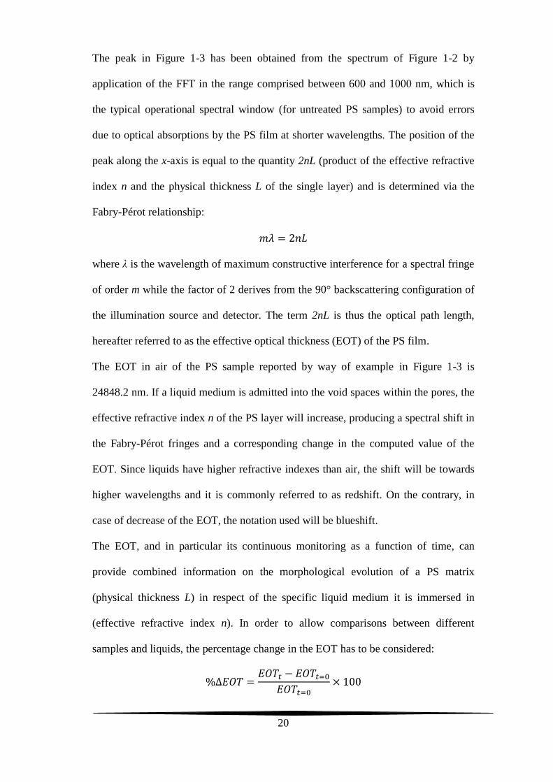
hereafter referred to as the effective optical thickness (EOT) of the PS film.
The EOT in air of the PS sample reported by way of example in Figure 1-3 is
24848.2 nm. If a liquid medium is admitted into the void spaces within the pores, the
effective refractive index n of the PS layer will increase, producing a spectral shift in
the Fabry-Pérot fringes and a corresponding change in the computed value of the
EOT. Since liquids have higher refractive indexes than air, the shift will be towards
higher wavelengths and it is commonly referred to as redshift. On the contrary, in
case of decrease of the EOT, the notation used will be blueshift.
The EOT, and in particular its continuous monitoring as a function of time, can
provide combined information on the morphological evolution of a PS matrix
(physical thickness L) in respect of the specific liquid medium it is immersed in
(effective refractive index n). In order to allow comparisons between different
samples and liquids, the percentage change in the EOT has to be considered:

21
where EOTt and EOTt=0 are measured at a given time t and at the initial time t = 0,
respectively. Therefore, in the ideal case of a PS sample completely stable in the
liquid environment it is in contact with, with no other interferences perturbing the
system, the profile of the %ΔEOT as a function of time will be simply represented by
a straight horizontal line parallel to the temporal x-axis and centered at the 0 value
along the y-axis. On the other hand, deviations from this value (or from a given
reference baseline) will be detected when the optical constants of PS change due, for
instance, to admission into the pores of a specific analyte during a sensing
experiment.
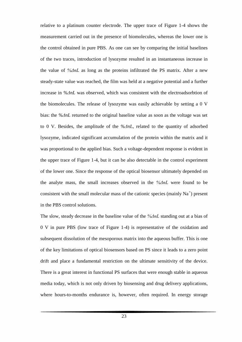
Figure 1-4 Percent variation in nL as function of time of a PS optical film with (upper trace) and
without (lower trace) introduction of 10 mg mL-1
lysozyme at t = 0. Taken from reference [20].

22
1.2.3 Biosensing
A demonstrative example of the sensing mechanism of a PS optical film is illustrated
in Figure 1-4. As previously mentioned, the mesoporous samples of the present
thesis have pore diameters which fall in the range 2-50 nm. Many proteins, enzymes
and antibodies have dimensions of the order of 10 nm; thereby, being the porous
material able to act as analyte capture matrix, meso-PS-based devices find a natural
application as biosensors. In the reported work [20], Chen and coworkers achieved
electric-field-assisted transport, capture, and interferometric sensing of biomolecules
by using a chemically modified (see following sections) nanostructurated optical film
of meso-PS. Electroadsorption was applied as analyte capture method, allowing the
device to simultaneously attract and detect (in buffer solutions) electrically charged
proteins, by application of an electrostatic potential opposite to their surrounding
one. A phosphate buffer saline (PBS) solution containing positively charged
lysozyme was circulated through the film, and a negative bias was applied in a series
of discrete steps to the PS-based sample in order to move and adsorb the
biomolecules to the pores walls. Bias was maintained at a given value (from -0.5 to -
2.75 V) for a total of 10 min, after which it was each time set back to the 0 V initial
value for 20 min. The Figure 1-4 reports the optical response of the sensor monitored
as a function of the time and the voltage provided. In this case, the percentage change
in the EOT was calculated through the formula:
where nLt,ΔV was measured at a given time t and applied bias ΔV, while nLt=0,ΔV=0 was
the value of nL measured from the sample in pure buffer solution at a time
immediately prior to introduction of protein (t = 0) and at an applied bias (ΔV) of 0 V
23
relative to a platinum counter electrode. The upper trace of Figure 1-4 shows the
measurement carried out in the presence of biomolecules, whereas the lower one is
the control obtained in pure PBS. As one can see by comparing the initial baselines
of the two traces, introduction of lysozyme resulted in an instantaneous increase in
the value of %ΔnL as long as the proteins infiltrated the PS matrix. After a new
steady-state value was reached, the film was held at a negative potential and a further
increase in %ΔnL was observed, which was consistent with the electroadsorbtion of
the biomolecules. The release of lysozyme was easily achievable by setting a 0 V
bias: the %ΔnL returned to the original baseline value as soon as the voltage was set
to 0 V. Besides, the amplitude of the %ΔnL, related to the quantity of adsorbed
lysozyme, indicated significant accumulation of the protein within the matrix and it
was proportional to the applied bias. Such a voltage-dependent response is evident in
the upper trace of Figure 1-4, but it can be also detectable in the control experiment
of the lower one. Since the response of the optical biosensor ultimately depended on
the analyte mass, the small increases observed in the %ΔnL were found to be
consistent with the small molecular mass of the cationic species (mainly Na+) present
in the PBS control solutions.
The slow, steady decrease in the baseline value of the %ΔnL standing out at a bias of
0 V in pure PBS (low trace of Figure 1-4) is representative of the oxidation and
subsequent dissolution of the mesoporous matrix into the aqueous buffer. This is one
of the key limitations of optical biosensors based on PS since it leads to a zero point
drift and place a fundamental restriction on the ultimate sensitivity of the device.
There is a great interest in functional PS surfaces that were enough stable in aqueous
media today, which is not only driven by biosensing and drug delivery applications,
where hours-to-months endurance is, however, often required. In energy storage

24
technologies, for instance, the search for new highly capacitive supports that could
withstand, without appreciable degradation, to electrolyte exposure for longer-term
periods (up to several years) is still an open issue.

1.3 Stabilization chemistries of porous silicon
One of the major barrier preventing commercial applications of PS is the instability
of its native surface. Hence, surface chemistry has proven to be a crucial element for
the technological success of this material.
Due to the huge surface area, PS is particularly susceptible to air or water oxidation,
as well as to contaminations by different types of species which can lightly or
heavily affect its properties. As confirmed by Fourier-transform infrared
spectroscopy measurements [10, 21], immediately after being electrochemically
etched, the surface of PS is covered with a passivating layer of Si−H bonds, with
minor quantities of Si−F and Si−O species. Such an as-formed surface is metastable,
and it reacts spontaneously with water vapor in the air even at room temperature. As
a consequence, a thin oxide (SiOx) layer will form within timescales of minutes.
Anyway, this is largely sufficient for transfer of freshly etched samples into inert-
atmosphere glove boxes and Schlenk lines for manipulation via wet chemical
techniques [10, 7].
The reactivity of PS is dominated by the chemistries of the Si−H and the Si−Si
bonds. Both of these species are able to reduce water, which is a competent oxidant
for PS. As already said, even water vapor has sufficient oxidizing potential to
spontaneously react, at room temperature, with the PS surface to form Si−O bonds. If
such a reaction is performed in liquid water, the nanophase SiOx can readily dissolve
due to hydrolytic attack. Indeed, hydroxide ions (OH-) attack both Si−H and Si−O
surface species and generate intermediates which then induce the Si−Si bond
cleavage. Depending on the application, much of the chemistry on PS has been
developed to minimize or to harness these oxidation reactions. The chemical
functionality of the reactive hydride species in pristine PS provides, however, a

26
versatile starting point for various reactions that can control the dissolution rate in
aqueous media. Presently, two are the most important approaches that have been
taken to stabilize PS: the first is to purposely oxidize it, while the second involves the
formation of Si−C bonds.
A variety of chemical or electrochemical oxidants and techniques can be used to
oxidize PS, such as gas-phase oxidations (like annealing with high-pressure water
vapor, rapid thermal oxidation, ozone) or oxidation induced by either cationic
surfactants or organic species. The simplest oxidant is air, which produces different
types of surface species, according to the temperature at which the reaction is
performed and the humidity of the air. At room temperature, the oxide layer grows
over the time assisted by stronger oxidants as ozone and nitrogen oxides present in
the atmosphere. Anyway, in some cases, the original freshly etched, hydrogen-
terminated PS surface can be quickly recovered by dipping the sample in an HF-
based solution. Air oxidation of PS is usually performed at high temperatures in
order to anneal and stabilize the Si−O bonds. Afterwards, the oxidized material can
be further modified using conventional silanol chemistries employed to modify silica
(SiO2) surfaces. However, an electronegative element such as oxygen somewhat
enhances the tendency of silicon to be attacked by nucleophiles, and Si−O bonds in
oxidized PS are still unstable in aqueous media because of hydrolytic attack. In
contrast, the low polarity of Si−C bonded species makes them kinetically inert
toward attack by water and hydroxides due to the low electronegativity of carbon.
Several different methods have been developed during the years to produce Si−C
bonds on PS surfaces, such as thermal or microwave-assisted hydrosilylation and
chemical or electrochemical grafting of Si−C species. Carbon covalently bonded to
silicon can impart good stability and a high degree of hydrophobicity to the surface,

27
providing a means to attach a wide variety of organic functional groups, sufficiently
hydrophobic that water is excluded from the immediate vicinity of the attachment
point. Si−C bonds are much less polar in respect with Si−O ones, and reactions that
form surface Si−C bonds show much greater resistance to attack by nucleophiles.
Nevertheless, both hydrosilylation than Si−C grafting suffer from the fact that they
do not completely remove all the Si−H species from the surface but rather merely
decorate it with functional groups. A number of surface reactive Si−Si and Si−H
species remain after the reactions, still accessible to aqueous solution. On the other
hand, silicon carbide is a well-known material that can yield very stable surface
species. It was this idea that inspired Salonen and coworkers to develop a
carbonization reaction for PS similar to those that produce silicon carbides [22].
Salonen’s “hydrocarbonized” surfaces are synthesized by high-temperature
decomposition of acetylene gas on as-prepared PS [22-24]. In a typical procedure,
freshly etched PS samples are thermally carbonized in a tube furnace at 450 °C for
30 min, with a constant flow of acetylene and nitrogen gas. The temperature of the
pyrolysis reaction plays a key role in determining the degree of hydrophobicity or
hydrophilicity of the samples. The resulting films are composed of an ill-defined
mixture of C−H, aromatic C=C, and C−OH species. Generally, they remained
enough porous to display Fabry-Pérot fringes for use as optical interferometric
sensors, as in case of the one presented in the previous section (Figure 1-4),
chemically modified according to the Salonen’s procedure [20]. Although less well-
defined than material prepared by hydrosilylation and grafting routes,
hydrocarbonized PS is environmentally stable and its chemical sensing capabilities
have been widely demonstrated [25-37]. Furthermore, Salonen’s carbonaceous
surfaces provide both conductive and biocompatible supports for protein
28
electroadsorption/desorption experiments like those performed by Chen and
coworkers, which are not possible to achieve by using freshly etched or oxidized PS
samples since they are, as well as not enough stable upon immersion in the liquid
solutions required by biomolecular complexes, semi and completely electrical
insulating materials, respectively. In the case of lysozyme loaded into a
hydrocarbonized PS optical sensor at an applied bias ΔV = -2.75 V for 120 min, more
than 80% of its enzymatic activity was, in fact, preserved after releasing the proteins
into free solution. Thus, this carbonization chemistry opened the door to similar tests
not only with different and eventually further functionalized biomolecules (to
improve biosensing selectivity and specificity), but also with other electrically
charged species for new interesting applications as, for instance, high-performance
rechargeable LIBs based on PS.

1.4 Nanostructured carbon/silicon hybrid
devices
In the last decade, especially after discovery of graphene in 2004 by Andre Geim and
Konstantin Novoselov at the Manchester University, carbon-based nanomaterials and
devices drew more attention than others by the scientific community, being still now
considered as the best candidates to substitute silicon-based systems in many diverse
applications. Most of the various allotropes of carbon share some peculiar properties
which can potentially make them new leading materials in different important
applied fields, in particular if occurring in a regularly ordered nanostructured
arrangement of the carbon atoms. High electrical conductivity and optical
transparency (graphene), mechanical strength and flexibility (carbon nanotubes) or
even superconductivity (buckminsterfullerenes) are just a few examples of the
advantages that these nanomaterials can offer over silicon-based ones [38].
1.4.1 Supercapacitors
Among so many prospects, one of the biggest and hardest challenges facing modern
research is to provide new systems able both to store than deliver more and more
energy at increasingly high rates. At present, graphitic (i.e. carbon-based) materials
are commonly employed as negative electrodes in the conventional LIBs used, for
instance, by the telecommunications electronics. Until now, their specific energy and
power capabilities turned out to be satisfactory enough to have permitted the
development of light in weight, portable and environmentally friendly batteries at an
acceptable cost to be commercially available. However, considerable improvements
are always more requested not only to decrease energy and time needed to recharge

30
state-of-the-art high-tech electronic devices, but also to meet the stronger demand of
energy storage required in other kinds of mobile or fixed applications, as in full
electric vehicles or solar harnessing technologies. In such a view, a very promising
answer can be again offered by carbonaceous materials, which are the most
investigated ones in order to make the so called supercapacitors [39].
Supercapacitors (also referred to as ultracapacitors) is a generally adopted name for
that class of devices capable to achieve energy densities several orders of magnitude
higher than traditional dielectric capacitors, having at the same time a power density
far larger than common LIBs and fuel cells. Supercapacitors are usually classified
into two main categories: (i) redox supercapacitors or pseudocapacitors and (ii)
electrochemical double layer capacitors. The basis of energy storage in the former
ones is Faradaic charge transfer. The electrical charge is built up via an electron
transfer mechanism producing changes in the chemical or oxidation state of the
electroactive material, according to Faraday’s laws related to the electrode potential.
Thus, they are somewhat battery-like in the behavior since the storage of electric
charge and energy is not electrostatic in origin (hence the prefix “pseudo”) but
deriving from electrochemical charge-transfer processes, involving the electrode
materials to undergo reversible Faradaic redox reactions during the charge/discharge
cycles. Generally used materials in redox supercapacitors are transition metal oxides
[40] (RuO2, Co3O4 or MnO2 and MnO3) or electronically conducting polymers [41]
(polyaniline, polypyrrole or derivatives of polythiophene) that can exhibit
significantly high pseudocapacitances, even though they often suffer of either poor
conductivity (metal oxides) or poor stability during cycling (polymers). By contrast,
in spite of a lower specific capacitance, carbon can impart at the same time high
conductivity and high stability in supercapacitative devices as the electrical double
31
layers [42-43]. As in common electrostatic capacitors, the energy storage mechanism
in these systems is simple charge separation, but resulting from the formation of an
electric double layer at the interface between an electronically conductive material
and the adjacent liquid electrolyte interposed between the anode and cathode
electrodes (also known as the solid-electrolyte interphase). In this case, the charge
process is not Faradaic, i.e. ideally no electron transfer takes place across the
electrode interface. In respect to conventional capacitors, the vast increase in
capacitance achievable by electrical double layer supercapacitors is principally a
function of two factors: (i) an extremely small distance separating the opposite
charges, as defined by the electric double layer; (ii) highly porous structured
electrodes that embody very high surface areas. Contrary to batteries, where charge-
transfer and chemical phase changes introduce additional relatively slow steps into
the process of energy storage and delivery, the mechanism in electrical double layers
is inherently rapid, as it simply involves movements of ions to and from the electrode
surface. Since a larger amount of energy can be stored within the pores of high
surface area materials, various porous forms of carbon are, therefore, usually
preferred. Activated carbons, carbon fibers and carbon aerogels are, to date, the most
widely utilized ones. In particular, ordered carbon nanostructures are recently
emerging as good candidates to make new supercapacitive devices, since their
nanoscale and readily accessible morphology can offer a unique combination of high
electrical conductivity and porosity, and shorten the transport path of ions and
electrons. As in sensing applications, where the properties of homogeneous carbon
nanostructures had been largely explored [44-45], the use as supercapacitative
electrodes of carbon nanofibers [46], single- [47] and multi-walled [48] carbon
nanotubes and, recently, graphene [49] has been demonstrated. Single-phased carbon
32
materials and nanostructures can potentially greatly enhance the cycling
performances of the anode and thus enormously extending lifetimes and
charge/discharge rates of products which make use of rechargeable batteries.
Nevertheless, their widespread application is essentially limited by the fact, as
mentioned before, that the capacitance values attainable thus far are still lower than
those of commercial LIBs.
1.4.2 Next-generation high-capacity lithium ion batteries
As far as traditional LIBs are concerned, a further new research trend aimed to
improve their performances has rapidly grown up in the last few years. In a different
perspective, heterogeneous nanostructured materials with multi-nanocomponents are
proposed [50-56], in order to synergically match the distinguishing properties of the
individual constituents. Each component can be, as a matter of fact, tailored to meet
different demands, e.g. high energy density and high conductivity. In such a way,
energy storage/delivery systems with very high capacitances can be, in principle,
fabricated without sacrificing cycle life or high power densities.
The major obstacle to the breakthrough of high-capacity LIBs is to find a reliable
replacement to graphite, the negative electrode commonly used in conventional
LIBs, which is affected by a limited reversible charge capacity of 372 mA h g-1
.
Materials forming alloys with lithium (like Sn, Sb, Ge, and Si) are potentially more
attractive anode candidates, since they can incorporate larger amounts of lithium
ions. Among lithium alloys, silicon is considered to be one of the next-generation
anodic materials for LIBs, since it is known to have the highest theoretical
gravimetric capacity at ~4200 mA h g-1
, a volumetric capacity of ~8500 mA h cm-3
,
and can offer an appropriate low voltage for an anode.

33
Silicon reacts with lithium to form binary alloys with a maximum uptake of 4.4
lithium atoms per silicon atom (Li22Si5). At room temperature, the highest achievable
specific capacity for silicon is 3579 mA h g-1
, far greater than the analogous value for
graphite. Nevertheless, crystalline silicon suffers from drastic volume changes during
lithium alloying (to form LixSi) and de-alloying (to reform Si) that has greatly
slowed down its application in this field. Upon insertion of lithium ions (lithiation),
silicon can expand volumetrically even up to 400% with anisotropic elongation along
the <110> direction, and it can contract significantly with the subsequent extraction
(delithiation). Repeated lithium insertion/extraction cycles invariably generate great
mechanical stress in the brittle silicon crystal lattice, leading to severe cracking that
makes the silicon electrodes lose contact with the current collector. Capacity fading
and pulverization of the structure are the consequences of such a gradual destruction,
which finally results in poor cyclability or even completely failure of the electrode.
Anyway, reducing the material size to the sub micrometer or nanometer range can
somewhat solve the problem mentioned above. Indeed, the internal strain in
incompact silicon nanostructures can be easily relaxed, without mechanical fracture,
because of their small size and the free surrounding space that becomes,
consequently, available.
Several different submicron and
nano morphologies of silicon have
been separately suggested to ease
the volume expansions during the
lithium ion insertion/extraction
cycling, including silicon sub Figure 1-5 Real-time in-situ transmission electron
microscopy images of a carbon/silicon
nanocomposite during lithium charging/discharging
cycles. Adapted from reference [54].

34
micrometer pillars, crystalline-amorphous nanowires arrays, nanotubes,
nanoparticles, thin films and PS [51-53]. Bare silicon nanostructures, in any case,
have two main drawbacks to be applied for LIBs: low electron conductivity (most of
all if undoped silicon structures) and low diffusivity for lithium ions. To overcome
these kinds of issues, an alternative strategy has been undertaken, i.e. adding a
covering layer with functional coating materials. In this case, the goal is, on one
hand, to enhance the charge transfer kinetics of the electrode and, on the other hand,
protect silicon from generating a solid-electrolyte interphase, thus preventing its
decrepitation upon cycling. Among other competitive options, a carbon-based
coating can be again a worthwhile choice, due to the good electrical conductivity of
carbon and its ability to accommodate silicon volume changes. More importantly, as
already stressed [42], the formation of a solid-electrolyte interphase involving a
porous carbon material can be, conversely to stark silicon, much more convenient,
since its pores are able both to host than furnish rapid access to a large number of
ions into the bulk. Furthermore, the additional porosity associated with a carbon
matrix can “sum” to the high surface area which can provide a nanomaterial like PS,
thus allowing dramatic increases in capacitance. Moreover, despite a more rigid and
heavy structure of silicon-based electrodes compared to carbon-based ones (causing
increases in the weight of the anode), a silicon skeleton is, most of the time,
particularly welcome as it is compatible with standard silicon technology. Otherwise,
a reverse configuration can be also expedient. By way of example, Figure 1-5 shows
very recently published results [54] about real-time phase transformation
investigations of single carbon nanofibers coated with amorphous silicon, made
possible by in situ transmission electron microscopy carried out during the
charge/discharge processes. Even just considering only silicon- and carbon-based
35
starting nanomaterials, a plenty of different morphologies, combinations and
architectures is conceivable. Each type of composite electrode has its pros and cons
and finding the optimal solution is still a great challenge to most of the researchers in
this field.
The nanostructuring and nanocomposition approaches briefly overviewed as yet keep
showing very encouraging results and might revolutionize future energy technologies
as in LIBs, even if the scale-up of these systems is, up to now, still far from meeting
industrial levels. In the depicted scenario, however, there is a shortcoming of fast and
cheap methods enabling to monitor in real time the structural evolution of
nanostructured matrices upon interaction with different testing electrolytes and
electrically charged species. From this point of view, a device inspired from the
sensing mechanism elaborated by Chen and coworkers [20] (formerly introduced in
the subsection 1.2.3) could potentially serve the purpose.
1.4.3 Porous silicon/carbon composite opto-electrochemical
sensors
Chen’s work could be thought as one pioneering attempt to address the optical
capabilities of PS towards the study, upon electrical perturbations, of electrically
complicated systems such as biomolecules-containing saline buffer solutions.
Although completely oriented to biomolecular sensing, the suggested platform can
be, anyway, extended to smaller charged atomic targets as ions.
Chen and coworkers successfully applied the Salonen’s thermal carbonization
chemistry [22] (see section 1.3) to a PS optical film in order to use it as an electro-
adsorptive substrate. The sensor was able to detect (by optical interferometry)
positively charged biomolecules, which retained their functional activity after being
36
released from the electrode surface. Nevertheless, the sensor was not applicable to
negatively charged molecules due to a lack of stability of the carbonized PS electrode
under positive bias conditions. Since this was not a fundamental limitation of the
carbon electrode, the causes of such instability were not further investigated.
Anyway, a number of other carbonization chemistries exist which can likewise work
inside the nanopores of a PS template. In particular, a very recently emerged one [57]
exploits one of the most common methods utilized to generate high surface area
carbons, which is pyrolysis of a carbon-containing resin or polymer. With the new
discovered technique, Kelly and coworkers took advantage of the peculiar
morphological structure of a PS rugate filter to mold the formation of characteristic
carbonized PS (CPS) composites, constituted by carbonized bundles of fibers
embedded into a periodic PS matrix. When combined with the signal transduction
properties of a PS photonic crystal, the film acted as highly sensitive optical vapor
sensor for volatile organic compounds. These CPS composites were shown to more
strongly adsorb organic vapors (e.g., toluene) than either freshly prepared or ozone-
oxidized porous silicon films, and the photonic properties of the rugate filter
provided a means to optically detect the adsorption event. Moreover, dissolution of
the PS skeleton generated arrays of free-standing glassy carbon nanofibers that
replicated the porosity of the template.
To the best of author’s knowledge, the stability of CPS composites produced through
the Kelly’s carbonization chemistry has not been systematically tried out, as yet,
neither in aqueous solutions nor under voltage applied. In the present work, Kelly’s
chemistry has been slightly modified to precisely control the final carbon content in
CPS samples, thus making them amenable for optical applications into a dynamic
microfluidic apparatus. The optimized procedure to fabricate reproducible CPS

37
composites will be following described and their characterization will be discussed.
The obtained CPS electrodes have been tested under stress conditions in different
liquids and polarizing them at different voltages. Due to the natural inclination of PS
as biomaterial, however, much of the effort has been spent to develop a highly
sensitive and reliable biosensor equivalent to the Chen’s one, providing results with
both positively than negatively charged biomolecules. Nevertheless, some tests
performed in pure saline ionic solutions will be also presented since, still to the
author’s personal opinion, this aspect deserved more attention. Furthermore, a
parallel electrical measurement configuration has been realized to simultaneously
acquire, during the sensing experiments, the electrochemical characteristic of the
device along with the optical one. New coupled opto-electrochemical sensors are
thus proposed to assist more expensive and time-consuming techniques in order to
better understanding the real-time behavior and performances of these nanosystems.

38
2 Fabrication and characterization of
porous silicon/carbon composite opto-
electrochemical sensors
In this chapter, an overview on the fabrication and characterization techniques of the
opto-electrochemical sensors subject matter of the present thesis will be given.
In the first section, the standard procedure to produce the starting PS samples will be
briefly summarized. For a complete and more detailed coverage about preparation
and characterization of PS optical films and used instrumentation the reader is
referred to [10]. The second section is devoted to the realization of CPS composites,
with particular attention to the expedients which have been adopted to make them
suitable for repeatable optical sensing applications. Lastly, in the third section, the
manufacturing of a real sensing device will be illustrated, by both describing the
various components than showing the coupled optical/electrical measurement system
that has been assembled for the sensing experiments.

2.1 From silicon to porous silicon
All the PS samples presented in this work have been prepared in the same way
according to the procedure described in [20], in order to obtain mesoporous single
layers with nominal pore diameters = 40 nm, thickness (L) = 9.8 µm, and porosity
(P) = 73%.
2.1.1 Four-point probe measurements of wafer resistivity
The preparation of PS samples starts from
4” crystalline (<100>-oriented) boron-
doped silicon wafers, in the present case
provided from Siltronix Corp. (Figure 2-
1). Since the PS films are designed for an
electrochemical use, the check and
determination of the effective electrical
resistivity of the pristine material is essential. Such an evaluation can be readily done
by a series of four-point probe measurements. A four-point configuration is required
in order to overcome contact resistance problems of a two-point one, which are due
to the high resistivity of native SiOx layers present on the surfaces of silicon starting
wafers.
A constant current (I) was passed between the outer two tips of the 4-point probe
head showed in Figure 2-1, while the voltage drop (V) was simultaneously measured
between the two inner ones. Afterwards, the obtained resistance values (V/I) were
converted to sheet resistance values (RS) by the relation:
Figure 2-1 A four-point probe head in contact
with a silicon wafer during a resistance
measurement.

40
where CF = 4.532 is a correction factor that is related to the sample geometry
(infinite sheet approximation). Finally, the resistivity ρ was calculated by the simple
formula:
where W is the measured thickness of the silicon wafer. The Table 1 reports some
representative values obtained in different spots of the same silicon wafer (W = 525
µm), from which all the PS samples that will be presented in this thesis have been
derived.
Table 2-1 Resistance and resistivity values measured on five different spots of a silicon wafer.
V/I (Ω) RS (Ω per square) ρ (Ω cm)
1 0.004375 0.019828 0.001041
2 0.004370 0.019805 0.001040
3 0.004347 0.019701 0.001034
4 0.004367 0.019791 0.001039
5 0.004325 0.019601 0.001029
Avg 0.004357 0.019745 0.001037
The average resistivity is about 1.04 mΩ cm, which corresponds to a highly doped
silicon wafer, often referred to as “degenerately” (p++
-type) doped.
2.1.2 Electrochemical etching of crystalline silicon
The silicon wafer was cleaved into smaller squared chips (1.5 X 1.5 cm2), each of
which was then electrochemically etched in order to fabricate a mesoporous single
layer.

41
The PS samples were produced by
electrochemical anodization of silicon in
an HF-based solution, the formation
involving reactions of Si−Si, Si−H, Si−O,
and Si−F bonds at the surface of the
silicon material. For such a type of highly
doped/low resistive silicon crystal the
etching mechanism is dominated by carrier tunneling [10].
A standard single-tank HF-resistant Teflon etch cell is pictured in Figure 2-2. The
sample, with a round exposed area of 1.2 cm2, was mounted inside the cell using an
aluminum foil as back-contact and a platinum loop as counter electrode. In such a
two-electrode configuration, the silicon chip serves as the anode. The sample was
then anodically etched in a solution of concentrated (48%) aqueous HF in anhydrous
ethanol (3:1 v/v HF:EtOH) by application
of a current density of 467 mA cm-2
for
48 s. Immediately after etching, it was
rinsed three times with ethanol, removed
from the electrochemical cell, and dried
in a stream of nitrogen gas.
A preliminary electropolishing step,
consisting of an electrochemical etch at a lower current density of 90 mA cm-2
for 30
s, was carried out each time before the above procedure to remove the top few nm of
silicon from the wafer surface. This turned out to be necessary in this case because of
the high doping level of the silicon original wafer, whose etching usually generates a
Figure 2-2 A conventional electrochemical cell
used to etch PS samples.
Figure 2-3 As-etched PS samples used in the
present work.
42
top crust of porous material with pores smaller than the rest of the film, presumably
due to segregation of dopants at the surface of the wafer. The sacrificial layer was
dissolved in a strongly basic solution (1 M aqueous NaOH), and the resulting silicon
chip was first rinsed with copious quantities of a lesser acid solution (1:1:3 v/v
HF:H2O:EtOH), then with ethanol and finally dried with nitrogen gas. Such a
procedure led to a particularly high degree of reproducibility of samples, which
exhibit a uniform brown-orange color at the final stage (Figure 2-3).
2.1.3 The spectroscopic liquid infiltration method (SLIM)
Several techniques exist in order to determine the morphological features of PS, such
as gravimetric measurements, scanning electron and probe microscopy, or nitrogen
adsorption analysis at cryogenic temperatures (e.g., the BET, BJH, and BdB
methods). Compared to these, the spectroscopic liquid infiltration method (SLIM)
constitutes a faster and, above all, nondestructive alternative, and it was therefore
adopted to check thickness L and porosity P of each freshly etched PS sample.
The SLIM is based on comparing data from two reflectance spectra: one obtained
from the sample in air (nM = nair = 1.000272 at 20 °C) and the other from the sample
immersed in a liquid of known refractive index (e.g. ethanol in this case, nM = nethanol
= 1.3611 at 20 °C). The overall apparatus to make these optical reflectance
measurements is photographically pictured in the inset of Figure 2-9. A split optical
fiber and lens set-up was used for both the illumination and the collection of the light
reflected from the sample. The optical reflectance spectra of the PS film were
acquired with a CCD-based spectrometer (Ocean Optics USB2000) attached to a
bifurcated fiber optic cable. A tungsten halogen light source (Ocean Optics R-LS-1),
providing a relatively broad effective wavelength range in the visible-near infrared
(400-1000 nm), was used to illuminate the surface of the sample via one arm of the

43
bifurcated fiber. The light source was focused by a bi-convex lens onto the sample
surface with a spot size of approximately 2 mm2, and the reflected light was
channeled to the spectrometer through the same objective lens. Thus, both the
spectral acquisition and light illumination were performed along the same axis,
normal to the surface of the PS sample.
Figure 2-4 FFT peaks derived from reflectance spectra in air (black) and ethanol (red) of a PS
film.
As a demonstrative example of how a SLIM analysis was usually performed, Figure
2-4 shows the FFTs of two reflectance spectra. The first is the one reported from
Figure 1-3 and measured in air (black peak) while the second is the FFT of the
reflectance spectrum measured from the same sample, but dipped in pure ethanol
(red peak). As one can see, immersion of the sample in ethanol results, at the same
time, in a redshift and attenuation of the peak. The position of the peak along the x-
axis represents the EOT of the film into the medium (air or ethanol), assuming the
pores within the light spot to have been completely wetted with ethanol. The EOT
shifts from a value in air EOTair = 24848.2 nm to a value EOTethanol = 30508.9 nm in
ethanol. Since spectra were acquired immediately after etching the PS samples, the
porous matrix is not oxidized and can be thought to be constituted by pure silicon.

44
Besides, considering the spectral region in which the FFT has been obtained (600-
1000 nm), its refractive index is substantially not wavelength-dependent and can be,
at the end, reasonably approximated to a value equal to nS = 3.8. A numeric
calculation which implements, therefore, a two-component (nS and nM) Bruggeman
effective medium approximation theory gives, as a result, values of thickness and
porosity equal to L = 9808 nm and P = 72.2% respectively, which are in this case
pretty close to the desired ones.
Although the SLIM provides a local evaluation of L and P only in the area irradiated
by the light spot (preferentially the center of the round PS chip) and it is not
representative of the entire film, it has been the main characterization procedure also
for samples in the subsequent fabrication steps, i.e. ozone oxidation and
carbonization (see following section).

2.2 From porous silicon to carbonized porous
silicon
All the PS samples presented in this work have been carbonized in the same way
according to the receipt described in the following sections, which lightly differs
from the original one developed by Kelly and coworkers in [57] (see subsection
1.4.3). In particular, great care has been paid in order to accurately control and vary
the final content of carbon of CPS composites, also avoiding all the time- or human-
dependent constraints which could affect somewhat their reproducibility.
2.2.1 The original carbonization procedure
As already mentioned in the introductory chapter, the carbon and CPS composites
templated by Kelly and coworkers in PS rugate filters were proposed for the
adsorption and detection of organic vapors. The process flow of Kelly’s method is
synthetically sketched in Figure 2-5:
Figure 2-5 Kelly’s carbonization chemistry process flow. Taken from reference [57].
Kelly’s CPS composites were synthesized by thermal degradation of one of the more
common polymers used as a precursor for amorphous carbon, i.e. the poly(furfuryl
alcohol). Freshly etched PS rugate filter templates were first oxidized under a stream
of ozone in order to provide strong adsorption sites for the furfuryl alcohol (FA)
carbon precursor. Then, the remaining pore volume was filled with a solution of
46
dihydrate oxalic acid in FA, whose in situ polymerization yielded a resin-infiltrated
film that was, at the end, carbonized at 700 °C for 5 h. These CPS composite
materials have shown to still retain some porosity, in spite of a reduction in the
average pore diameter. While the aim of such a former work was to achieve an as
much large amount of carbon as possible within the pores of the rugate filter vapor
sensors, the main requirement of the present one was rather to reach a compromise
between the final carbon content of the samples and their optical transduction
capabilities. Indeed, being carbon a strong light absorber, an excessive quantity of
carbon might lead to the complete depletion of Fabry-Pérot interference fringes in a
~10 µm thick PS optical film immersed in liquid. For this reason, here the FA had
been diluted in a solvent, i.e. ethanol, providing different kinds of samples with
different percentages of carbon (see next chapter), depending on the initial
concentration of the neat precursor.
2.2.2 Ozone oxidation and furfuryl alcohol infiltration
The FA polymerization is acid-catalyzed. As confirmed by Fourier-transform
infrared spectroscopy analysis [10], an oxidative treatment on PS with ozone can
provide a silicon oxide surface with a high percentage of terminal silanol
functionality (Figure 2-5). Ozone oxidation gives quite hydrophilic PS surfaces and
forms oxides more hydrated than in thermal oxidation procedures. In the original
carbonization receipt, oxalic acid (in concentration equal to 5 mg mL-1
) was added to
the FA precursor to improve the chemical kinetics of the subsequent polymerization.
Anyway, the surface protons within a just ozone-oxidized PS sample have been
found to be sufficiently acidic to catalyze, on your own, the reaction. Therefore, the
present-work samples were simply oxidized in a flow of ozone gas (with a flow rate
of 1.5 SCFH), at room temperature, for a period of 20 min. After checking thickness

47
and porosity with the SLIM, the resulting red-colored oxidized PS chips (Figure 2-6)
were blocked on the chuck of a spin-coating system, programmed to run a two-steps
rotation. 100 µL of neat or diluted FA were gently spilled on the surface of the
samples, which were initially spun at a frequency of 300 rpm for 1 min, then at 3000
rpm for two min. The former slower rotation step was intended to favor the
infiltration of the carbon precursor into the nanopores of the film, while the faster
one to mechanically dry the excess amount of FA, avoiding the formation of
aggregates on top of sample surfaces.
Samples prepared in this way look very
uniform and without patches of alcohol
residue, even by spinning neat FA.
Anyway, the final CPS composites did
not display Fabry-Pérot fringes unless the
percentage of FA relative to the total
volume of solution was below a threshold value of 25% (1:3 v/v FA:EtOH).
2.2.3 Thermal polymerization and carbonization
Immediately after being spun, the FA-impregnated PS samples were put into a
covered ceramic container and loaded inside the chamber of a box oven (Thermo
Scientific Thermolyne FD1535M, right portion of Figure 2-7) set to reach a target
temperature of 70 °C with a ramp rate of 10 °C/min. Thus, they were left there for 16
h (the time starting as soon as the target temperature was reached) in an indoor air
atmosphere. During this period, the FA undergoes an acid-catalyzed thermal
polymerization process, yielding poly(FA) infiltrated PS films.
Figure 2-6 Ozone oxidized PS sample before
FA infiltration.

48
Figure 2-7 Box oven and tube furnace utilized for the polymerization and carbonization steps,
respectively. The inset shows some CPS composite chips at the final stage.
Once the 16 hour time was elapsed, samples were removed from the box furnace,
placed on a ceramic crucible and introduced in a tube furnace (Thermo Scientific
Lindberg Blue M, left down corner of Figure 2-7) sealed up with a corked tube. In
order to purge the furnace of oxygen, nitrogen gas was flowed for 30 min at a rate of
1 SLPM and at a temperature of 50 °C (10 °C/min). Afterwards, under the same
nitrogen flow, the temperature was again increased at a rate of 10 °C/min up to 700
°C, and the poly(FA)-PS composites carbonized at this temperature for 55 min.
Finally, the furnace was set to cool to room temperature at a ramp rate of 5 °C/min
and the samples removed at 200 °C to avoid cracking due to thermal shocks. The
inset of Figure 2-7 shows how the dark CPS chips appear after the entire preparation
was completed. As it will be better highlighted in the next chapter, the extent of the
carbon layer thickness synthesized within the CPS optical chips was simply
estimated by considering the final FFT interferometric peak intensities displayed by
samples. Unlike more specific quantitative or carbon-based typical analysis, as
energy-dispersive X-ray or Raman spectroscopies, this fast characterization does not
49
provide any information about the carbon form produced, but it was performed on all
the fabricated samples and allows rapid comparisons.
It has to be underlined that the just described carbonization procedure has been
nearly optimized in order to better control the final carbon content inside CPS
composites, not to improve the performances of the ultimate device or the economy
of the process. For instance, a mild oxidation for few minutes at low temperature,
like the one carried out using ozone as oxidant, tends to produce electrical insulating
oxides, in principle not suitable for electric-field-assisted experiments. Anyway, the
oxide layers forming in these conditions were probably very thin since they seem to
have not affected the electroadsorbtion/desorption measurements. Besides, the ozone
oxidation usually improves mechanical stability in PS, and the control of the carbon
content is easier by harnessing only the acid groups deriving from the ozone
oxidation as catalyzing agents. Even if the use of oxalic acid can substitute or be
associated to the ozone oxidative step, the presence of this compound in the FA
precursor could trigger an uncontrolled polymerization even at room temperature,
leading also to limitations in samples reproducibility. Still concerning the FA
polymerization, despite some indications suggesting the 70 °C thermal process does
not need such a long incubation period of 16 hours, this step has been maintained
since it takes place in air atmosphere, it is not gas-consuming and can be easily
performed overnight. By contrast, the nitrogen flow related to the 700 °C pyrolysis
procedure is the most critical parameter of the entire process in order to control as
fine as possible the carbon coating layer thicknesses. The carbonization period has
been drastically reduced from 5 hours to less than one not since this time turned out
to be largely sufficient to produce good optical (and stable) CPS chips, as well as it is
gas-saving and more verifiable. In this case, the more important origins of error in

50
reproducibility can stem from a wrong sample positioning inside the furnace (causing
undesired temperature gradients if it is far from the tube furnace center) or oxygen
contaminations, which can lead to too much carbonaceous materials or, in the worst
case, even to the complete combustion of the sample.
Despite some ad hoc tests had been performed to compare pros and cons and
feasibility of modified carbonization techniques, the results are not definitive and go
beyond the scope of the present thesis.
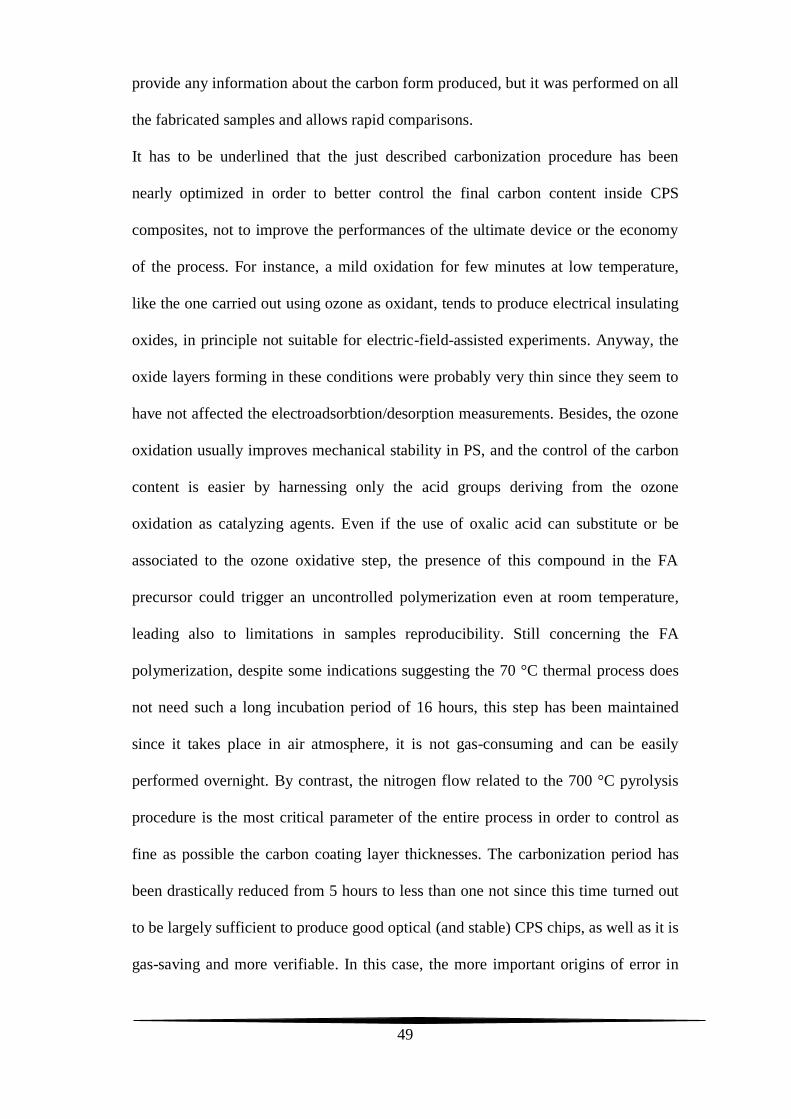
2.3 Porous silicon/carbon coupled opto-
electrochemical sensors
The CPS composite chips were mounted inside a custom-designed flow cell (Figure
2-8) joined with a peristaltic pump (inset of Figure 2-9) to allow circulation of
analyte-containing or free liquid media in
a closed loop.
The total volume of liquid employed in
all the experiments was equal to 5 mL
and it was mechanically agitated at a flow
rate of about 1 mL min-1
. The flow cell
was optically transparent to facilitate
acquisition of reflectance spectra by the same instrumentation used for the SLIM
determinations previously described (see subsection 2.1.3). The chip was contacted
on the backside with a strip of aluminum foil, enabling its use as working electrode.
Instead, a customized platinum counter electrode had been expressly designed to be
fitted inside the flow cell rig and circularly shaped to improve electric field
uniformity. In order to avoid leakages, the platinum loop was directly drawn inside
the inner portion of a circular O-ring, also provided by a homemade reference
electrode (a silver chloride wire) allowing measurements in a three-electrode
configuration, as well as in a two-electrode one. Nevertheless, in the present thesis,
only two-electrode measurements will be presented, in order to facilitate
comparisons. Therefore, the electrodes were connected to a general purpose
electrochemical potentiostat/galvanostat (Pine Instrument Company AFCBP1) set to
Figure 2-8 Opto-electrochemical flow cell.

52
work in potentiostatic conditions. The current analog output was transferred from the
bipotentiostat to a computer-controlled analog-to-digital card by a programmable
current/voltage source (Keithley 2601 Sourcemeter), interfaced with a customized
LabVIEW program expressly written to collect the values of the current flowing
between the CPS working electrode and the platinum counter electrode as a function
of time.
The overall combined optical/electrical measurement system that has been assembled
for the time-resolved tests is showed in Figure 2-9. Electrical data were collected at a
ratio of 10 acquisitions per s. On the other hand, unless noted otherwise, optical data
were typically acquired every 10 s by the CCD spectrometer software (Ocean Optics
OOIBase32) and preliminary processed and monitored by a purpose-written program
macro (Wavemetrics IGOR Pro). Optical and electrical parameters (timescales,
applied bias, sweep rates) as well as sensing ones (pH, ionic strengths, buffer
solutions, biomolecular complexes, concentrations) will be specified in the next
chapter for each proposed experiment.
Figure 2-9 Overview of the whole instrumentation system. The inset zooms on the combined
opto-electrochemical device.

53
3 Experimental results
The present chapter reports some test experiments accomplished with the new
described opto-electrochemical combined sensors, aimed to demonstrate their
usefulness both in sensing than in energy harvesting applications.
In as much as sensing fields are concerned, the admission into and diffusion through
nanoscale pores by molecules is a fundamental process of great importance, for
instance, to bioanalytics and separations science. The constricted environment in a
nanopore has a substantial influence on molecular transport that can be harnessed for
filtration [58-59], controlled release, nanofluidic [60] or gating applications [61-62].
Artificial systems with abiotic micro- or nanometer sized pores (e.g., polymeric,
inorganic, and composite membranes) designed to take advantage from such
processes are usually more stable and predictable compared to biological pores [63].
Among these, PS offer a versatile synthetic alternative to control analyte transport
and binding: (i) the high surface area of the 3D material allows to capture and
concentrate significant quantities of target molecules, (ii) the porous nanostructure
can be tuned during synthesis to yield a range of pore sizes, and (iii) optical
structures can be incorporated into the film to provide sensitive, label-free
quantification of analyte binding. The drive to decrease sample volumes and increase
throughput has led to microanalysis PS-based chips that combine these components
within a volume of a few cubic micrometers. In addition, conventional analytical
techniques like chromatography or electrophoresis tend to remove the separation
process from the detection event, both spatially than temporally. PS Fabry-Pérot
optical films provide, in this case, a means to detect and identify molecules
54
simultaneously with, and in the same ultrasmall physical location as, the separation
event, thus improving sensing fidelity in complex media.
The size-selective filtration and separation abilities of PS have been demonstrated for
a wide range of molecular species [64-65]. In a former work [66], by exploiting the
native negative charge of thermally oxidized PS optical chips, Chen and coworkers
succeeded to admit or exclude (from nanophase pores) different kinds of proteins
based on their size and charge. Each biomolecule displays a surface charge
distribution depending on factors as its chemical configuration or pH and ionic
strength of solutions biomolecular complexes are dissolved in. As formerly showed,
capture/release events and transport of electrically charged proteins can be even
better controlled if assisted by an electric field applied to a conductive Salonen- or
Chen-like material, yielding to a very powerful support to identify biomolecules
based on their size, charge, and diffusional characteristics. Nevertheless, Chen’s
electroadsorption/desorption results do not provide any information about the current
behavior of the device along with the optical sensing. A parallel electrical assay can
be used not only to monitor the evolution of a PS matrix in different ionic liquids
upon voltage application, but also work as an additional transduction method in case
one of the two, for whichever reason, failed.

3.1 Tuning the carbon content and preliminary
stability tests
The two main prerequisites expected from a conventional working electrode are
stability in electrolytic solutions and conductivity. A carbon film upholstering the
pore walls of a PS-based electrode and synthesized through the Kelly’s carbonization
chemistry can meet both of these two requirements.
The final carbon amount lining the present-work CPS composites depends on the
initial quantity of the FA carbon precursor casted on top of the PS surface. For a CPS
sample to display Fabry-Pérot fringes, the FA had not been used neat but it was
diluted in ethanol. According to the carbonization procedure described in the
previous chapter, CPS layers did not display any interferometric optical pattern if the
relative percentage of FA respect to the 100 µL total volume solution was higher
than a threshold value, approximately estimated to be around 25%. Therefore, in the
present thesis, the FA percent range investigated to produce CPS optical chips had
been limited in a window comprised between 1% and 25%. Figure 3-1 shows several
FFT interferometric peaks, each one corresponding to a CPS film characterized by
the carbon precursor percentage marked by color.

56
Figure 3-1 FFT peaks in air of CPS films containing a different percentage of carbon. The inset
is the magnification corresponding at the higher concentrations: 20% (green line) and 25%
(dark blue line), respectively.
The peaks of Figure 3-1 are FFTs from CPS reflectance spectra all collected in air. In
this case, the shift in the EOT (2nL) between one peak and another is due to
inequalities in the physical thickness L of the original PS samples. Increasing the FA
quantity into the reaction solution means to increase the carbon amount will be
present on the CPS composite, and thus the light absorption capabilities of the final
sensor. The higher the carbon content is, the lower is the amplitude of the Fabry-
Pérot interferometric fringes, and so the intensity of the corresponding FFT peak.
Even a very small percentage (e.g., 1%) of carbon precursor leads to pretty dark
samples and to a significant depletion of the FFT intensity. By augmenting the
carbon content, a monotonic decrease of the FFT peak intensities is observed until
the higher percentages are reached. In these cases, as from the inset of Figure 3-1
showing the magnification of the 20% and 25% FFTs, the intensities were very low
but peaks could still be used for interferometric sensing.
In the two previous chapters, it has been widely stressed that water is a huge
corrosive agent for freshly etched or oxidized PS, and that a carbon layer can protect

57
PS surfaces from hydrolithic attack. Chen’s samples, hydrocarbonized according to
the Salonen’s method, demonstrated a pretty good stability in aqueous buffers, as
well as upon application of different voltages. Nevertheless, as formerly mentioned,
they were not stable in case of positive potential. For this reason, the stability of the
new Kelly’s composites has been tried out under positive bias, continuously applied
between the working and the counter electrodes, with samples always immersed in
reference deionized water (pH = 5.3 at 23.2 °C). Figure 3-2 shows the optical method
that has been used in this case to check stability of the present-work sensors,
consisting in monitoring the percent changes in the EOT as a function of time.
Figure 3-2 Changes in EOT of CPS optical films as a function of time. A constant +1 V potential
was applied in water to the different carbon-containing CPS electrodes.
After 30 min samples were immersed in liquid, +1 V was applied to the CPS
electrode and optical data acquired, in this case, every 30 s. Due to the very long
timescales and the optical nature of such a stability test, a voltage lower than the

58
water electrolysis potential difference (1.23 V) was chosen in order to avoid water
splitting effects. Samples and carbon percentages from Figure 3-2 are the same of
Figure 3-1. All the CPS films displayed remarkable endurances under these rather
extreme stress conditions. In order to make adequate comparisons, two factors have
to be taken into account when considering the %ΔEOT variations: the blueshift
decrease (indicating a dissolution of the PS matrix), and their amplitudes (related to
the final sensitivity of the sensor). Of course, samples with minor quantities of
carbon undergo faster degradation, whose rate is proportional to the carbon content.
By contrast, increasing the carbon amount leads to almost completely stable samples,
but at the expense of the optical signal quality. Anyway, even a 1% CPS sample can
withstand up to more than eleven hours in these conditions, by showing an overall
blue shift of less than 0.5%.
Table 3-1 Linear fit parameters resulting from linear interpolation of data from Figure 3-2.
Carbon % Slope (10-6
) Standard
Error (10-8
)
RSS Pearson’s
r
Adjusted R2
1 -13.394 1.11428 0.02912 -0.99955 0.99909
5 -8.44459 0.975442 0.07002 -0.99884 0.99768
10 -4.47958 0.886472 0.08391 -0.99628 0.99256
15 -1.76583 5.91607 2.19887 -0.58924 0.34682
20 -2.97173 7.26562 5.79716 -0.68179 0.46456
25 -0.948481 25.3606 52.5894 -0.0881 0.00721
As it appears well-rendered by the CPS composites with the lowest carbon
percentages (1%, 5% and 10%), the slow dissolution of a CPS matrix has, in these
conditions, a linear trend. Table 3-1 reports results from linear regression valuations
computed for all the five carbon percentages. A more strict statistical calculation
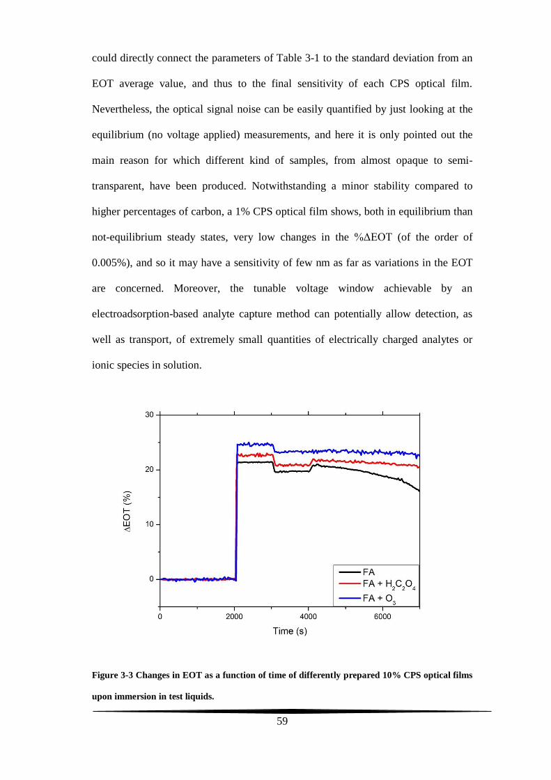
59
could directly connect the parameters of Table 3-1 to the standard deviation from an
EOT average value, and thus to the final sensitivity of each CPS optical film.
Nevertheless, the optical signal noise can be easily quantified by just looking at the
equilibrium (no voltage applied) measurements, and here it is only pointed out the
main reason for which different kind of samples, from almost opaque to semi-
transparent, have been produced. Notwithstanding a minor stability compared to
higher percentages of carbon, a 1% CPS optical film shows, both in equilibrium than
not-equilibrium steady states, very low changes in the %ΔEOT (of the order of
0.005%), and so it may have a sensitivity of few nm as far as variations in the EOT
are concerned. Moreover, the tunable voltage window achievable by an
electroadsorption-based analyte capture method can potentially allow detection, as
well as transport, of extremely small quantities of electrically charged analytes or
ionic species in solution.
Figure 3-3 Changes in EOT as a function of time of differently prepared 10% CPS optical films
upon immersion in test liquids.

60
Finally, some quick stability tests performed in various (stationary) liquids are
presented in Figure 3-3. The samples were three same percentage (10%) CPS
composites, synthesized by using a different catalysis strategy for the polymerization
process: (i) ozone (blue line), (ii) 5 mg mL-1
oxalic acid (red line) and (iii) neither
ozone nor oxalic acid (black line). Optical reflectance spectra were collected first in
air to establish a common initial horizontal baseline in the %ΔEOT value.
Afterwards, ethanol was poured on top of the samples surfaces in order to wet their
pores walls, this resulting into a swift redshift of the EOT at time t = 2000. After a
new steady value was reached, ethanol was substituted with deionized water and then
with sodium hydroxide at pH = 13, a very basic solution generally used to dissolve
PS films. The noisy behavior corresponding to a CPS sample prepared both with
ozone than oxalic acid is not displayed in Figure 3-3 for clarity reasons. The
composites were prepared in the same way according to the procedure described in
the previous chapter, including the 70 °C polymerization period 16 h long. The only
film that undergoes significant degradation over this timescale is the one for which
any catalyzing agent has been used to polymerize the FA. By comparison, the other
two show a longer stamina to nucleophilic attack by NaOH hydroxide ions (OH-),
even if they will, anyhow, start to dissolute after a short while, most likely because of
the pretty low carbon content. The choice of ozone over oxalic acid was preferred, as
previously explained, to better control reproducibility of samples.

3.2 Electrochemical measurements of double-
layer capacitances
Information about capacitance of an electrochemical system can be gained by
applying an electrical perturbation to it and observing the resulting changes in its
current vs time characteristic.
Figure 3-4 Current transient resulting from a -0.5 V potential step on a 20% CPS sample. The
inset shows the corresponding natural logarithm of the current vs time trace.
The capacitance of a CPS composite is defined by the electrical double-layer in the
electrolytic solution. A two-electrode cell can be approximated by an electrical
circuit with a resistor, RS, representing the solution resistance and a capacitor, Cd,
representing the double layer at the CPS/electrolyte interface. Since Cd is generally
potential dependent, the proposed model in terms of circuit elements is strictly
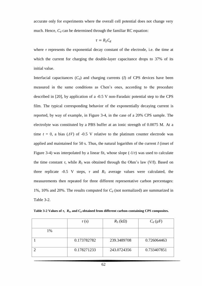
62
accurate only for experiments where the overall cell potential does not change very
much. Hence, Cd can be determined through the familiar RC equation:
where τ represents the exponential decay constant of the electrode, i.e. the time at
which the current for charging the double-layer capacitance drops to 37% of its
initial value.
Interfacial capacitances (Cd) and charging currents (I) of CPS devices have been
measured in the same conditions as Chen’s ones, according to the procedure
described in [20], by application of a -0.5 V non-Faradaic potential step to the CPS
film. The typical corresponding behavior of the exponentially decaying current is
reported, by way of example, in Figure 3-4, in the case of a 20% CPS sample. The
electrolyte was constituted by a PBS buffer at an ionic strength of 0.0075 M. At a
time t = 0, a bias (ΔV) of -0.5 V relative to the platinum counter electrode was
applied and maintained for 50 s. Thus, the natural logarithm of the current I (inset of
Figure 3-4) was interpolated by a linear fit, whose slope (-1/τ) was used to calculate
the time constant τ, while RS was obtained through the Ohm’s law (V/I). Based on
three replicate -0.5 V steps, τ and RS average values were calculated, the
measurements then repeated for three different representative carbon percentages:
1%, 10% and 20%. The results computed for Cd (not normalized) are summarized in
Table 3-2.
Table 3-2 Values of τ, RS, and Cd obtained from different carbon-containing CPS composites.
τ (s) RS (kΩ) Cd (µF)
1%
1 0.173782782 239.3489708 0.726064463
2 0.178271233 243.0724356 0.733407851

63
3 0.174013517 245.2182442 0.709627124
Avg 0.175355844 242.5222312 0.723050597
10%
1 0.320277745 69.8031551 4.588298973
2 0.303616375 71.33685262 4.25609434
3 0.281565617 71.18451025 3.955433794
Avg 0.301819912 70.76806945 4.264916574
20%
1 1.257924927 8.786110916 143.1719835
2 1.294196821 8.778089888 147.4349019
3 1.123418788 9.097194425 123.4906869
Avg 1.225180179 8.884676894 137.8981131
By considering an overall area of ~1.2 cm2, the final values of Cd for 1%, 10% and
20% CPS composites were found to be equal to (0.603 ± 0.001), (3.55 ± 0.26) and
(115 ± 10) µF cm-2
, respectively. The values are visualized in the graph of Figure 3-5
as a function of the carbon content percentage.

64
Figure 3-5 Dependence of the interfacial capacitance of CPS composites on the carbon content.
The obtained values are of the same order of magnitude of Chen’s device, whose
interfacial capacitance Cd was measured to be ~8 µF cm-2
(τ = 0.4 s, RS = 50 kΩ).
However, the ease in increasing the FA precursor achievable by the present
carbonization method suggests, as somewhat foreseeable, a not linear dependence
between carbon content and capacitance, which can be rapidly enlarged as it is
shown in Figure 3-5. Anyhow, the results can furnish additional clear evidences
about reliability of the carbon tuning process and, as a consequence, on the
reproducibility of the CPS fabrication method.

3.3 Coupled opto-electrochemical biosensing
Ionic strength and pH are two important parameters as far as electric-field-assisted
biosensing experiments are concerned. The buffer ionic strength window explored by
Chen and coworkers in [20] ranged from 0.001 to 0.15 M. Only buffer solutions (pH
6.7) with ionic strength of 0.007 M, anyway, were used in all the experiments
addressed to quantify protein loading and concentration efficiency as a function of
applied bias and bulk solution concentration. Therefore, for all the measurements
presented in the current section as well, an equivalent ionic strength value was
chosen (7.5 mM), and obtained by mixing the PBS (Invitrogen) buffer with ultrapure
deionized water (final pH = 7.5 at 22.9 °C).
An as such as medium-low ionic strength value is preferred, in this case, in order to
lower the sensor optical response stemming from the ionic salts present into the
buffers, trying at the same time to do not denature or otherwise deactivate the
biomolecule of interest. Buffered solutions are indeed necessary to keep the correct
pH for many biomolecular complexes to work, as enzymes. If the pH moves outside
of a very precise narrow window, for instance, the enzymes can undergo significant
denaturation which can be even permanently disable their catalytic activity. On the
other hand, buffers as PBS contain a number of inorganic salts (such as KH2PO4,
NaCl, Na2HPO4) that, once dissolved in water, form electrically charged species
which may interfere with the optical based interferometric detection of
electroadsorbed/desorbed molecules that is harnessed by the CPS sensors. For this
reason, a check in pure buffer turns out to be strictly necessary in these kinds of
measurements, especially when a lot of different parameters are involved.

66
Figure 3-6 Optical response of a 10% CPS sensor upon electric-field-assisted test with positively
charged lysozyme.
Chicken lysozyme (molecular weight ≈ 14.3 kDa, isoelectric point ≈ pH 11) was
selected also for these studies as a test protein, and used as-received (Sigma-Aldrich)
without further purification. At pH = 7.5, lysozyme exhibits a net positive charge and
can be therefore attracted by applying a negative potential to a CPS film. The Figure
3-6 illustrates the generally adopted procedure for the detection of electroadsorbed
enzyme, by using a 10% CPS optical sensor. An initial horizontal baseline was
established in pure buffer solution holding the film at 0 V. A negative bias (-2.75 V)
was then applied just in PBS (1000 s) and maintained for about 8 min. Afterwards,
the voltage was set back to 0 V until a new equilibrium was reached (2000 s). Hence,
a solution containing lysozyme, at a concentration of 10 mg mL-1
and dissolved in
the identical buffer, was introduced into the flow cell system (2000 s) with the film
still held at 0 V. As soon as a new steady state was established, the same negative

67
bias of the control test was applied (2500 s) and kept from the same period (500 s).
The %ΔEOT profile of Figure 3-6 shows three different sharp redshifts: the first (at
~1000 s) is ascribable, in first approximation, to cationic Na+ atoms still present into
the control buffer; the second (~2000 s) is relative to lysozyme infiltrating the CPS
matrix for normal diffusion; the third (~2500 s), instead, is consistent with a voltage-
dependent electroadsorption phenomenon driving protein into the pores. In this case,
the greater contribution to the optical signal given by lysozyme respect to ionic
species can be roughly estimated by looking at the differences between the baselines
values of Figure 3-6. However, such an evaluation is oftentimes not so easy, since
many are the parameters which can affect the final result, such as the magnitude and
sign of the charge on the ions, biomolecules and applied bias. In particular, unlike
Chen’s composites, where the ionic strength of the electrolyte was found to exert
only a minor effect, the optical response of the present-work sensors turned out to be,
as showed in Figure 3-6, strongly influenced by ions. Anyway, a parallel electrical
assay can help to better understanding these phenomena. Apart from providing an
additional check for those measurements lacking of such a clear evidence, it can also
be used to test the electrochemical performances of the device.
3.3.1 Positively charged biomolecules
Lysozyme is a relatively small globular protein with dimensions of 3.0 nm X 3.0 nm
X 4.5 nm and an isoelectric point of pH 11.1, which exhibits a net positive charge if
dissolved in a buffer below this pH. Therefore, it is a very good candidate to test the
opto-electrochemical behavior of a CPS sensor under different conditions. Figure 3-7
displays an experiment, equivalent to the one presented above, in the case of a 1%
CPS coupled device, for which both the optical (a) than electrical (b) characteristics
are provided.
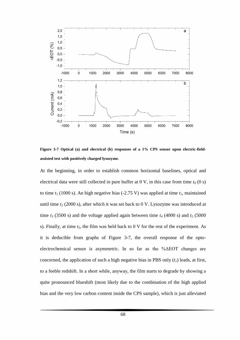
68
Figure 3-7 Optical (a) and electrical (b) responses of a 1% CPS sensor upon electric-field-
assisted test with positively charged lysozyme.
At the beginning, in order to establish common horizontal baselines, optical and
electrical data were still collected in pure buffer at 0 V, in this case from time t0 (0 s)
to time t1 (1000 s). An high negative bias (-2.75 V) was applied at time t1, maintained
until time t2 (2000 s), after which it was set back to 0 V. Lysozyme was introduced at
time t3 (3500 s) and the voltage applied again between time t4 (4000 s) and t5 (5000
s). Finally, at time t5, the film was held back to 0 V for the rest of the experiment. As
it is deducible from graphs of Figure 3-7, the overall response of the opto-
electrochemical sensor is asymmetric. In so far as the %ΔEOT changes are
concerned, the application of such a high negative bias in PBS only (t1) leads, at first,
to a feeble redshift. In a short while, anyway, the film starts to degrade by showing a
quite pronounced blueshift (most likely due to the combination of the high applied
bias and the very low carbon content inside the CPS sample), which is just alleviated

69
by setting the bias back to 0 V (t2). Introduction of lysozyme (t3) results in an
instantaneous increase in the value of %ΔEOT as long as protein infiltrated the
porous matrix. After equilibrium, a large redshift is observed upon repeating
application of the negative bias (t4). The %ΔEOT profile reaches a saturation value
around the time at which the electrode was held back to 0 V (t5). After that, a
blueshift takes place, as steep as the prior redshift but more abrupt of the one
observed in PBS. Despite these results are similar to those presented in the previous
experiment (Figure 3-6), it is not as simple, in this case, to determine the quantity of
electradsorbed lysozyme. Although the %ΔEOT variation first increases (t4) and then
returns (t5) to the value established by the previous baseline at 0V, suggesting that
biomolecules were successfully captured into the CPS matrix and then released back
into the bulk solution, it is hard to discriminate between the contributions coming
from protein rather than ions to the redshift observed at time t4, due to the large
blueshift taking place between time t1 and t3. On the other hand, by looking at the
current characteristic (Figure 3-7-b), the electrical response of the sensor with respect
to ions (t1) and ions plus lysozyme (t4) is specular to the optical one. In this case,
charging effects, akin to those formerly showed (Figure 3-4), are observed both in
PBS than in the presence of lysozyme. By comparing the two graphs of Figure 3-7, it
can be gathered that sample degradation in pure buffer ultimately depends on high
charging currents involving the CPS/electrolyte interface. These effects are high in
PBS, but can be attenuated in the presence of lysozyme infiltrated into the film, thus
leading to an even more stable material. Summarizing, the combined methods are
both sensitive to low quantities of ionic species and electrically charged
biomolecules into aqueous solutions, the optical displaying a higher response to
biomolecules and a lower one to ions, and vice-versa the electrical. In principle, such

70
a coupled technique can be used to specify how much of the biosensor optical
response derives from biomolecules and how much from ions. Otherwise, it provides
a means to characterize biomolecules based on their electrical transport features.
Anyway, the system is here presented just as a proof of concept and tried out under
different stress conditions.
Time-resolved results as the ones from Figure 3-7 were obtained by synchronizing
the electrical with the optical response of the sensor. In order to appreciate tiny
redshifts like the one observed at time t1, it was not applied a spike potential but bias
was gradually decreased from 0 down to -2.75 V (t1 and t4) and back (t2 and t5) at a
pretty low rate (10 mV s-1
). Indeed, occurring into a dynamic liquid environment, the
optical signal needs more time respect to the electrical one to stabilize into an
averaged value. As a consequence, optical data are somewhat delayed compared to
the current measurements. Performances and resolution of the device have been thus
tested again with positively charged lysozyme by varying the applied voltage rate,
i.e. exploring its behavior at low (10 mV s-1
), medium (25 mV s-1
) and high (50 mV
s-1
) values. The outcome of this trial is reported in the graphs of Figure 3-8, in the
case of a 10% CPS sensor.

71
Figure 3-8 Optical (a) and electrical (b) responses of a 10% CPS sensor upon electric-field-
assisted test with positively charged lysozyme, varying the potential between -1 V and +1 V.
This case, lysozyme was introduced at time t = 500 s, still resulting into an abrupt
increase of the %ΔEOT. Initially, the potential was swept between -1 V and +1 V at
the lowest rate for three times (as a guide to the eye, at ~2000 s). After an
equilibrium period (during which the film was always held at 0 V), bias was again
applied in the same window (-1 V, +1 V) but increasing the rate and number of
repeats as well. Figure 3-8 shows a good correspondence between optical and
electrical measurements in this range. Despite the investigated bias frequency values
were very low (2.5 mHz, 6.25 mHz and 12.5 mHz, respectively), the %ΔEOT profile
displays a periodic modulation which is directly linked to the current measurements.
As in the preceding experiments (Figures 3-6 and 3-7), to a negative bias
corresponds a redshift in the optical thickness (the current values of Figure 3-8-b are
reported, in this case, inverted respect to those of Figure 3-7-b). By progressively

72
passing from -1 V to +1 V, the current flow changes direction and a blueshift occurs
as long as bias come back to 0 V and, then, to -1 V again. In so far as the first (out of
three) voltage ramp at 2.5 mHz is concerned, such blueshift has probably two
different causes: the former can be seen as electrostatic repulsion between positively
charged lysozyme and CPS surface upon application of a positive voltage, which
implies that infiltrated proteins are repelled from the porous layer; whilst the latter
involves a degradation of the film rather under positive than negative bias conditions.
Anyway, the other two voltage ramps carried out at 2.5 mHz seem to be symmetric
respect to -1 V and +1 V, relative to the steady baseline value the %ΔEOT will reach
at 0 V. The behavior observed for the following voltage ramps carried out at 6.25
mHz and 12.5 mHz (at ~4000 s and ~6000 s, respectively) is almost equivalent,
except for the amplitude modulation of the optical signal, which decreases with
increasing frequency. Besides, in spite of using lower bias and a sample with a
higher carbon content, a gradual abatement in the baseline value is observed after
each series of voltage ramps, revealing an overall small degradation of the sample
over the time. However, the optical signal keeps a good correlation with the
frequency modulation in every step (2.5 mHz, 6.25 mHz and 12.5 mHz) and the
optical biosensor demonstrates to be thus sensitive to current sign changes in this
window.
3.3.2 Negatively charged biomolecules
Bovine serum albumin (BSA) is a medium-sized molecule (14.0 nm X 3.8 nm X 3.8
nm, molecular mass ≈ 66 kDa) with an isoelectric point of 4.7. By using the same
PBS buffer at pH 7.5, a clear negative charge distribution should surround the
protein. Therefore, it would be expected to adsorb to a CPS electrode held at a
positive bias. As formerly stated, Chen’s samples exhibited significant corrosion at
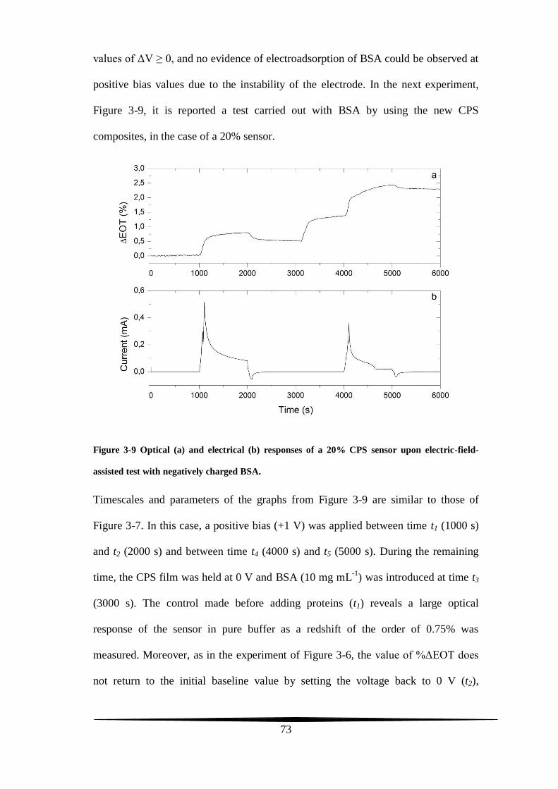
73
values of ΔV ≥ 0, and no evidence of electroadsorption of BSA could be observed at
positive bias values due to the instability of the electrode. In the next experiment,
Figure 3-9, it is reported a test carried out with BSA by using the new CPS
composites, in the case of a 20% sensor.
Figure 3-9 Optical (a) and electrical (b) responses of a 20% CPS sensor upon electric-field-
assisted test with negatively charged BSA.
Timescales and parameters of the graphs from Figure 3-9 are similar to those of
Figure 3-7. In this case, a positive bias (+1 V) was applied between time t1 (1000 s)
and t2 (2000 s) and between time t4 (4000 s) and t5 (5000 s). During the remaining
time, the CPS film was held at 0 V and BSA (10 mg mL-1
) was introduced at time t3
(3000 s). The control made before adding proteins (t1) reveals a large optical
response of the sensor in pure buffer as a redshift of the order of 0.75% was
measured. Moreover, as in the experiment of Figure 3-6, the value of %ΔEOT does
not return to the initial baseline value by setting the voltage back to 0 V (t2),

74
suggesting that some ionic species were irreversibly adsorbed on the CPS surface.
Infiltration of BSA (t3) leads to a slight higher redshift compared, and approximately
the same increase is observed upon application of the positive voltage (t4), even if the
profile is different. Again, as at time t2, a tiny blueshift can be detected setting the
bias to 0 V (t5), indicating that a very small quantity of negative charged species
were released in these conditions. The fidelity in detection of
electradsorbed/desorbed negatively charged biomolecules can be in principle
improved increasing the voltage applied, the protein concentration and by using a
molecule with a lower isoelectric point. Pepsin is a medium-small enzyme
(molecular weight ≈ 34.6 kDa) with an isoelectric point as low as 1.0. Graphs from
Figure 3-10 refer to a test for which the molar concentration of negatively charged
pepsin was greatly increased, trying to approach the one used for lysozyme in the
experiments of Figures 3-7 and 3-8 (~700 µM). The results are again presented in the
case of a 20% CPS sensor.
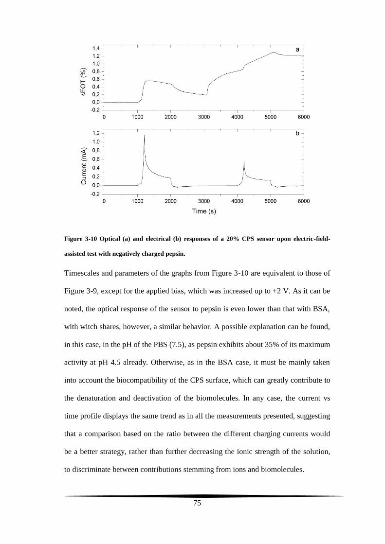
75
Figure 3-10 Optical (a) and electrical (b) responses of a 20% CPS sensor upon electric-field-
assisted test with negatively charged pepsin.
Timescales and parameters of the graphs from Figure 3-10 are equivalent to those of
Figure 3-9, except for the applied bias, which was increased up to +2 V. As it can be
noted, the optical response of the sensor to pepsin is even lower than that with BSA,
with witch shares, however, a similar behavior. A possible explanation can be found,
in this case, in the pH of the PBS (7.5), as pepsin exhibits about 35% of its maximum
activity at pH 4.5 already. Otherwise, as in the BSA case, it must be mainly taken
into account the biocompatibility of the CPS surface, which can greatly contribute to
the denaturation and deactivation of the biomolecules. In any case, the current vs
time profile displays the same trend as in all the measurements presented, suggesting
that a comparison based on the ratio between the different charging currents would
be a better strategy, rather than further decreasing the ionic strength of the solution,
to discriminate between contributions stemming from ions and biomolecules.

76
Conclusions
The stability in aqueous media of new nanostructured carbon/silicon composites,
synthesized through the Kelly’s carbonization chemistry, has been demonstrated, its
dependence on the carbon content investigated in the range 1-25% by an optical
method. Endurance and electrical conduction capabilities of the nanoelectrodes have
been tried out under stress in liquid and upon application of different bias, both
negative than positive. The measurements show encouraging results even for very
low carbon quantities, suggesting their testing with higher carbon amounts, as well as
with specific stability studies for energy harvesting applications, such as cyclic
voltammetry. The feasibility to fabricate highly stable and sensitive optical
interferometric sensors, based on electroadsorption as analyte capture technique, has
been confirmed. Experiments with both negatively than positively charged
biomolecular targets have been presented, and a parallel opto-electrochemical
configuration has been set up to examine responses and performance of the device.
Finally, an upgraded platform to identify biomolecules based on their size, charge,
diffusional, and electrochemical characteristics has been proposed.

References
1. Watanabe Y, Arita Y, Yokoyama T, Igarashi Y: FORMATION AND
PROPERTIES OF POROUS SILICON AND ITS APPLICATION.
Journal of the Electrochemical Society 1975, 122.
2. Ito T, Yamama A, Hiraki A, Satou M: SILICIDATION OF POROUS
SILICON AND ITS APPLICATION FOR THE FABRICATION OF A
BURIED METAL LAYER. Applied Surface Science 1989, 41-2.
3. Anderson RC, Muller RS, Tobias CW: INVESTIGATIONS OF POROUS
SILICON FOR VAPOR SENSING. Sensors and Actuators a-Physical
1990, 23.
4. Canham LT: SILICON QUANTUM WIRE ARRAY FABRICATION BY
ELECTROCHEMICAL AND CHEMICAL DISSOLUTION OF
WAFERS. Applied Physics Letters 1990, 57.
5. Lehmann V, Gosele U: POROUS SILICON FORMATION - A
QUANTUM WIRE EFFECT. Applied Physics Letters 1991, 58.
6. Hamilton B, Jacobs J, Hill DA, Pettifer RF, Teehan D, Canham LT: Size-
controlled percolation pathways for electrical conduction in porous
silicon. Nature 1998, 393.
7. Stewart MP, Buriak JM: Chemical and biological applications of porous
silicon technology. Advanced Materials 2000, 12:859-869.
8. Singh N, Karambelkar A, Gu L, Lin K, Miller JS, Chen CS, Sailor MJ, Bhatia
SN: Bioresponsive Mesoporous Silica Nanoparticles for Triggered Drug
Release. Journal of the American Chemical Society 2011, 133.
9. Lin VSY, Motesharei K, Dancil KPS, Sailor MJ, Ghadiri MR: A porous
78
silicon-based optical interferometric biosensor. Science 1997, 278.
10. Sailor MJ: Porous Silicon in Practice. Wiley-VCH Verlag & Co. KGaA
2012.
11. Anglin EJ, Schwartz MP, Ng VP, Perelman LA, Sailor MJ: Engineering the
chemistry and nanostructure of porous Silicon Fabry-Perot films for
loading and release of a steroid. Langmuir 2004, 20.
12. Theiss W, Henkel S, Arntzen M: CONNECTING MICROSCOPIC AND
MACROSCOPIC PROPERTIES OF POROUS-MEDIA - CHOOSING
APPROPRIATE EFFECTIVE-MEDIUM CONCEPTS. Thin Solid Films
1995, 255.
13. Wu J, Sailor M: Chitosan Hydrogel-Capped Porous SiO2 as a pH
Responsive Nano-Valve for Triggered Release of Insulin. Advanced
Functional Materials 2009, 19.
14. Pacholski C, Perelman LA, VanNieuwenhze MS, Sailor MJ: Small molecule
detection by reflective interferometric Fourier transform spectroscopy
(RIFTS). Physica Status Solidi a-Applications and Materials Science 2009,
206.
15. Pacholski C, Yu C, Miskelly GM, Godin D, Sailor MJ: Reflective
interferometric Fourier transform spectroscopy: A self-compensating
label-free immunosensor using double-layers of porous SiO2. Journal of
the American Chemical Society 2006, 128.
16. Pacholski C, Sartor M, Sailor MJ, Cunin F, Miskelly GM: Biosensing using
porous silicon double-layer interferometers: Reflective interferometric
Fourier transform spectroscopy. Journal of the American Chemical Society
2005, 127.

79
17. Mun K-S, Alvarez SD, Choi W-Y, Sailor MJ: A Stable, Label-free Optical
Interferometric Biosensor Based on TiO2 Nanotube Arrays. Acs Nano
2010, 4.
18. Schwartz MP, Alvarez SD, Sailor MJ: Porous SiO2 interferometric
biosensor for quantitative determination of protein interactions: Binding
of protein a to immunoglobulins derived from different species.
Analytical Chemistry 2007, 79.
19. Alvarez SD, Li C-P, Chiang CE, Schuller IK, Sailor MJ: A Label-Free
Porous Alumina Interferometric Immunosensor. Acs Nano 2009, 3.
20. Chen MY, Klunk MD, Diep VM, Sailor MJ: Electric-Field-Assisted Protein
Transport, Capture, and Interferometric Sensing in Carbonized Porous
Silicon Films. Advanced Materials 2011, 23.
21. Rao AV, Ozanam F, Chazalviel JN: INSITU FOURIER-TRANSFORM
ELECTROMODULATED INFRARED STUDY OF POROUS SILICON
FORMATION - EVIDENCE FOR SOLVENT EFFECTS ON THE
VIBRATIONAL LINEWIDTHS. Journal of the Electrochemical Society
1991, 138:153-159.
22. Salonen J, Bjorkqvist M, Laine E, Niinisto L: Stabilization of porous silicon
surface by thermal decomposition of acetylene. Applied Surface Science
2004, 225.
23. Salonen J, Laine E, Niinisto L: Thermal carbonization of porous silicon
surface by acetylene. Journal of Applied Physics 2002, 91.
24. Salonen J, Lehto VP, Bjorkqvist M, Laine E, Niinisto L: Studies of
thermally-carbonize porous silicon surfaces. Physica Status Solidi a-
Applied Research 2000, 182.
80
25. Bjorkqvist M, Paski J, Salonen J, Lehto VP: Temperature dependence of
thermally-carbonized porous silicon humidity sensor. Physica Status
Solidi a-Applications and Materials Science 2005, 202.
26. Bjorkqvist M, Salonen J, Laine E: Humidity behavior of thermally
carbonized porous silicon. Applied Surface Science 2004, 222.
27. Bjorkqvist M, Salonen J, Paski J, Laine E: Characterization of thermally
carbonized porous silicon humidity sensor. Sensors and Actuators a-
Physical 2004, 112.
28. Jalkanen T, Torres-Costa V, Salonen J, Bjorkqvist M, Makila E, Martinez-
Duart JM, Lehto V-P: Optical gas sensing properties of thermally
hydrocarbonized porous silicon Bragg reflectors. Optics Express 2009, 17.
29. Salonen J, Tuura J, Bjorkqvist M, Lehto VP: Sub-ppm trace moisture
detection with a simple thermally carbonized porous silicon sensor.
Sensors and Actuators B-Chemical 2006, 114.
30. Kaukonen AM, Laitinen L, Salonen J, Tuura J, Heikkila T, Limnell T,
Hirvonen J, Lehto V-P: Enhanced in vitro permeation of furosemide
loaded into thermally carbonized mesoporous silicon (TCPSi)
microparticles. European Journal of Pharmaceutics and Biopharmaceutics
2007, 66.
31. Heikkila T, Salonen J, Tuura J, Kumar N, Salmi T, Murzin DY, Hamdy MS,
Mul G, Laitinen L, Kaukonen AM, et al: Evaluation of mesoporous TCPSi,
MCM-41, SBA-15, and TUD-1 materials as API carriers for oral drug
delivery. Drug Delivery 2007, 14.
32. Bjorkqvist M, Salonen J, Laine E, Niinisto L: Comparison of stabilizing
treatments on porous silicon for sensor applications. Physica Status Solidi
81
a-Applied Research 2003, 197.
33. Salonen J, Kaukonen AM, Hirvonen J, Lehto V-P: Mesoporous silicon in
drug delivery applications. Journal of Pharmaceutical Sciences 2008, 97.
34. Salonen J, Laitinen L, Kaukonen AM, Tuura J, Bjorkqvist M, Heikkila T,
Vaha-Heikkila K, Hirvonen J, Lehto VP: Mesoporous silicon
microparticles for oral drug delivery: Loading and release of five model
drugs. Journal of Controlled Release 2005, 108.
35. Lehto VP, Vaha-Heikkila K, Paski J, Salonen J: Use of thermoanalytical
methods in quantification of drug load in mesoporous silicon
microparticles. Journal of Thermal Analysis and Calorimetry 2005, 80.
36. Salonen J, Paski J, Vaha-Heikkila K, Heikkila T, Bjorkqvist M, Lehto VP:
Determination of drug load in porous silicon microparticles by
calorimetry. Physica Status Solidi a-Applications and Materials Science
2005, 202.
37. Ruminski AM, King BH, Salonen J, Snyder JL, Sailor MJ: Porous Silicon-
Based Optical Microsensors for Volatile Organic Analytes: Effect of
Surface Chemistry on Stability and Specificity. Advanced Functional
Materials 2010, 20.
38. Mostofizadeh A, Li Y, Song B, Huang Y: Synthesis, Properties, and
Applications of Low-Dimensional Carbon-Related Nanomaterials.
Journal of Nanomaterials 2011.
39. Pandolfo AG, Hollenkamp AF: Carbon properties and their role in
supercapacitors. Journal of Power Sources 2006, 157.
40. Lokhande CD, Dubal DP, Joo O-S: Metal oxide thin film based
supercapacitors. Current Applied Physics 2011, 11.

82
41. Ghenaatian HR, Mousavi MF, Rahmanifar MS: High performance hybrid
supercapacitor based on two nanostructured conducting polymers: Self-
doped polyaniline and polypyrrole nanofibers. Electrochimica Acta 2012,
78.
42. Merlet C, Rotenberg B, Madden PA, Taberna P-L, Simon P, Gogotsi Y,
Salanne M: On the molecular origin of supercapacitance in nanoporous
carbon electrodes. Nature Materials 2012, 11.
43. Lufrano F, Staiti P: Mesoporous Carbon Materials as Electrodes for
Electrochemical Supercapacitors. International Journal of Electrochemical
Science 2010, 5.
44. Park HG, Hwang S, Lim J, Kim D-H, Song IS, Kim JH, Woo DH, Lee S, Jun
SC: Comparison of Chemical Vapor Sensing Properties between
Graphene and Carbon Nanotubes. Japanese Journal of Applied Physics
2012, 51.
45. Zuo J, Yao W, Liu X, Qin J: Sensing Properties of Carbon Nanotube-
Carbon Fiber/Cement Nanocomposites. Journal of Testing and Evaluation
2012, 40.
46. McDonough JR, Choi JW, Yang Y, La Mantia F, Zhang Y, Cui Y: Carbon
nanofiber supercapacitors with large areal capacitances. Applied Physics
Letters 2009, 95.
47. Izadi-Najafabadi A, Yasuda S, Kobashi K, Yamada T, Futaba DN, Hatori H,
Yumura M, Iijima S, Hata K: Extracting the Full Potential of Single-
Walled Carbon Nanotubes as Durable Supercapacitor Electrodes
Operable at 4 V with High Power and Energy Density. Advanced
Materials 2010, 22.

83
48. Frackowiak E, Metenier K, Bertagna V, Beguin F: Supercapacitor
electrodes from multiwalled carbon nanotubes. Applied Physics Letters
2000, 77.
49. Liu C, Yu Z, Neff D, Zhamu A, Jang BZ: Graphene-Based Supercapacitor
with an Ultrahigh Energy Density. Nano Letters 2010, 10.
50. Thakur M, Pernites RB, Nitta N, Isaacson M, Sinsabaugh SL, Wong MS,
Biswal SL: Freestanding Macroporous Silicon and Pyrolyzed
Polyacrylonitrile As a Composite Anode for Lithium Ion Batteries.
Chemistry of Materials 2012, 24.
51. Zhao Y, Liu X, Li H, Zhai T, Zhou H: Hierarchical micro/nano porous
silicon Li-ion battery anodes. Chemical Communications 2012, 48.
52. Guo J, Sun A, Wang C: A porous silicon-carbon anode with high overall
capacity on carbon fiber current collector. Electrochemistry
Communications 2010, 12.
53. Astrova EV, Fedulova GV, Smirnova IA, Remenyuk AD, Kulova TL,
Skundin AM: Porous silicon based negative electrodes for lithium ion
batteries. Technical Physics Letters 2011, 37.
54. Wang C-M, Li X, Wang Z, Xu W, Liu J, Gao F, Kovarik L, Zhang J-G,
Howe J, Burton DJ, et al: In Situ TEM Investigation of Congruent Phase
Transition and Structural Evolution of Nanostructured Silicon/Carbon
Anode for Lithium Ion Batteries. Nano Letters 2012, 12.
55. Cui L-F, Yang Y, Hsu C-M, Cui Y: Carbon-Silicon Core-Shell Nanowires
as High Capacity Electrode for Lithium Ion Batteries. Nano Letters 2009,
9.
56. Zhao C, Li Q, Wan W, Li J, Li J, Zhou H, Xu D: Coaxial carbon-silicon-
84
carbon nanotube arrays in porous anodic aluminum oxide templates as
anodes for lithium ion batteries. Journal of Materials Chemistry 2012, 22.
57. Kelly TL, Gao T, Sailor MJ: Carbon and Carbon/Silicon Composites
Templated in Rugate Filters for the Adsorption and Detection of Organic
Vapors. Advanced Materials 2011, 23.
58. Striemer CC, Gaborski TR, McGrath JL, Fauchet PM: Charge- and size-
based separation of macromolecules using ultrathin silicon membranes.
Nature 2007, 445.
59. Han J, Fu J, Schoch RB: Molecular sieving using nanofilters: Past, present
and future. Lab on a Chip 2008, 8.
60. Abgrall P, Nguyen NT: Nanofluidic devices and their applications.
Analytical Chemistry 2008, 80.
61. Basore JR, Lavrik NV, Baker LA: Single-Pore Membranes Gated by
Microelectromagnetic Traps. Advanced Materials 2010, 22.
62. Tokarev I, Minko S: Stimuli-Responsive Porous Hydrogels at Interfaces
for Molecular Filtration, Separation, Controlled Release, and Gating in
Capsules and Membranes. Advanced Materials 2010, 22.
63. Schoch RB, Bertsch A, Renaud P: pH-Controlled diffusion of proteins with
different pl values across a nanochannel on a chip. Nano Letters 2006, 6.
64. Orosco MM, Pacholski C, Sailor MJ: Real-time monitoring of enzyme
activity in a mesoporous silicon double layer. Nature Nanotechnology
2009, 4.
65. Rong G, Weiss SM: Biomolecule size-dependent sensitivity of porous
silicon sensors. Physica Status Solidi a-Applications and Materials Science
2009, 206.

85
66. Chen MY, Sailor MJ: Charge-Gated Transport of Proteins in
Nanostructured Optical Films of Mesoporous Silica. Analytical Chemistry
2011, 83.

86
Acknowledgements/Ringraziamenti
This material is based upon research supported by Scuola Interpolitecnica di
Dottorato, Politecnico di Torino, INRIM, Nanofacility Piemonte (a laboratory
supported by Compagnia di San Paolo), and UCSD. As it stems from a particularly
large number of collaborations and projects, a lot of people must be acknowledged
for all the works performed during this PhD.
First of all, I wish to express my deepest gratitude to three persons: Dr. Luca
Boarino, Dr. Andrea M. Rossi and Prof. Michael J. Sailor. Their friendship over the
years allows me to go on the other side of the world and it is the primary reason that
made of San Diego one of the best experience of my life. Luca and Andrea taught me
the fundamentals of research and how to deal with issues in nanotechnology,
demonstrated unexpected consideration and trust on me, invaluable guidance and
support in a way that now I consider them more friends than supervisors. More
importantly, when I asked for a training abroad and in spite of being understaffed and
overworked, they did not hesitate a second by catapulting me to learn from one of the
best in this field. I will be always beholden to them for this. Professor Sailor
welcomed me in his labs as well as at his home, lunches or dinners with warmth,
congeniality and outstanding availability. Although he was busy or even saturated
with different projects, he found the time for a weekly personal meeting which
significantly contributed to increase my scientific awareness. Above all, I’m
thanking Prof. Sailor for each “good job, Dario” he said. This really helped me and
instilled in me the necessary confidence I needed and I usually lack in. It has been
87
great, fun and a privilege to have Luca, Andrea and Mike as my special masters and
examples.
Secondly, I want to thank both my Italian than American “mentors” who directly
faced my fat-head: Andrea M. Giovannozzi, Emanuele Enrico, Annalisa Nastro,
Michelle Y. Chen and Chia-Chen Wu. Thank you guys for all your teachings,
suggestions, help and smiles. I take the opportunity to thank all the present and
former members of the Sailor’s research group too, in particular: Vinh M. Diep,
Nobuhiro Yagi, Andrea Potocny, Alejandra Nieto, Matt Kinsella, James S. Ha and
Luo Gu. Of course, I’m particularly grateful to all my colleagues and friends at
INRIM with which I shared very nice moments, in particular: Roberto Rocci,
Natascia M. De Leo, Federica Celegato, Matteo Fretto, Matteo Bruna, Stefano Borini
and Giampiero Amato.
The official reviewing of this thesis was done by Prof. Claudia Pacholski and
Professor Michael J. Sailor, who are gratefully acknowledged along with my
academic tutor Prof. Fabrizio C. Pirri.
Infine, desidero ringraziare immensamente la mia famiglia per il supporto, l’affetto e
l’incoraggiamento di questi anni, mio papà, mio fratello Max, Giorgia e i miei zii
Nanni e Rosa. E ancora tutti i miei amici che mi sono sempre stati accanto,
soprattutto nei momenti difficili. Anche questa tesi, ad ogni modo, è dedicata
esclusivamente ad una sola persona. Grazie mamma, ti voglio bene.
Torino, February 2013.
Dario Imbraguglio

88
PhD Publications and Awards

Imbraguglio et al. Nanoscale Research Letters 2012, 7:530http://www.nanoscalereslett.com/content/7/1/530
NANO EXPRESS Open Access
Submicron machining and biomoleculeimmobilization on porous silicon by electronbeamDario Imbraguglio*, Andrea Mario Giovannozzi, Annalisa Nastro and Andrea Mario Rossi
Abstract
Three-dimensional submicrometric structures and biomolecular patterns have been fabricated on a porous siliconfilm by an electron beam-based functionalization method. The immobilized proteins act as a passivation layeragainst material corrosion in aqueous solutions. The effects' dependence on the main parameters of the process(i.e., the electron beam dose, the biomolecule concentration, and the incubation time) has been demonstrated.
Keywords: Porous silicon, Electron beam, Lithography, Micromachining, BiomoleculesPACS: 87.85.Va
BackgroundElectron beam lithography (EBL) is known to be apattern-designing technique of integrated electrical cir-cuits, with writing resolution even down to tens of nan-ometers, which allows the fabrication of innovative andadvanced devices for nanotechnological applications[1,2]. In EBL procedures, electron-sensitive polymericresists are usually spun on top of samples' surfaces priorto irradiation in a scanning electron microscope (SEM).Depending on the nature of the resist, the irradiatedgeometry or its specular negative is used as a mask forsubsequent material etching or deposition steps in orderto obtain structures with nanometer-scale features.However, the EBL, when directly used to desorb chem-ical species from a surface, can be also exploited as alocal functionalization method [3] to create molecularmodified or biopatterns without employing any resist.This has been the case, for instance, of porous silicon(PS) surface-based biosensors [4].PS is a silicon nanosponge produced by electrochem-
ical etching of crystalline silicon in a hydrofluoric (HF)acid-containing solution. It is one of the most investi-gated structures in nanomaterials science due to somefascinating properties which can be harnessed in manyapplied research fields [5]. Morphological parameters of
* Correspondence: [email protected] Division, Istituto Nazionale di Ricerca Metrologica, Stradadelle Cacce 91, Torino 10135, Italy
© 2012 Imbraguglio et al.; licensee Springer. ThCommons Attribution License (http://creativecoreproduction in any medium, provided the orig
PS matrices, i.e., pore sizes, porosity (voids-to-total vol-ume ratio), and thickness, can be easily controlled justby varying the experimental electrochemical conditions(such as current density, HF concentration, or etchingduration), allowing the use of PS for size-selective filtra-tion or separation processes, drug delivery, or sensingapplications.The huge specific surface area (in the order of 200 m2/
cm3) of PS is hydride-terminated in as-etched samples[6,7], and a well-established modification chemistry hasbeen developed in the past years to selectively bind largeamounts of different target analytes within the pores [8].In so far as biological species are concerned, theimmobilization of proteins [9], enzymes [10], and anti-bodies [11] on PS surfaces can be achieved by differenttechniques. Among the ones which allow submicro-metric definitions, the EBL has already proved its cap-ability in designing chemical and biopatterns solely onselected and very small region of PS [3,4], opening thepossibility of future development of highly-sensitivenanobiosensors and multiplexed analysis based on thismaterial. From this perspective, PS is a very convenientsubstrate for EBL processes because of its porous struc-ture. Indeed, due to the lower quantity of Si atoms withrespect to an equal volume of bulk Si, PS behaves as alow-density material and exhibits a reduced proximityeffect [2], which is the main limitation factor in writingresolution with standard EBL-based methods. Moreover,
is is an Open Access article distributed under the terms of the Creativemmons.org/licenses/by/2.0), which permits unrestricted use, distribution, andinal work is properly cited.

Imbraguglio et al. Nanoscale Research Letters 2012, 7:530 Page 2 of 8http://www.nanoscalereslett.com/content/7/1/530
the absence of the polymeric resist during irradiation fur-ther contains the phenomenon because the only cause ofoverexposure of PS irradiated regions stems from sec-ondary and backscattered electrons just coming from theunderlying PS/Si substrate. This means that moredefined and small patterned features can be, in principle,obtained by direct, i.e., not resist-mediated, irradiation ofPS. Therefore, by combining EBL nanostructuring cap-abilities with those of PS whose pore dimensions can bevaried from the macro- to the microscale (<2 nm),sophisticated optical nanostructures could, in principle,be fabricated, such as three-dimensional (3D) photoniccrystals, waveguides, or optical gratings.As far as the application of the direct EBL method on
PS is concerned, some previous works have alreadydemonstrated its capability in material structuring[12,13] as well as the feasibility to fabricate a reliablebiosensor [4]. Different kinds of geometries had beenpatterned on PS surfaces, and the control of featuredimensions is possible by tuning the process parameters.Furthermore, proteins which were bound on PS surfacesby such a resistless EBL technique had been shown toretain their full functionality after the process and canact as bioreceptors for molecular and biomolecular ana-lytes. We report on recent studies and advances on bothsides, i.e., the (submicron) machining and theimmobilization of biomolecules on PS. The obtainedresults let us discover a new and intriguing property ofthe interaction between biomolecular species and asolid-state nanomaterial which, to the best of our know-ledge, has never been observed before.
MethodsPS single-layer films have been anodically etched fromhighly boron-doped single-crystal Si wafers <100> (resist-ivity ranging from 0.008 to 0.012 Ω cm) in a 1:2 solutionof aqueous 50% HF/ethanol in volume; the electrochem-ical etching procedure is described in several papers [3-5].Typically, a double-step etching/stop loop (consisting of0.2-sec etching at a current density of 400 mA/cm2 fol-lowed by a 10-sec stop etching time) was repeated, thenumber of times depending on the desired film thickness,using a Keithley 2400 SourceMeter (Keithley InstrumentsInc., Cleveland, OH, USA). PS samples with thicknesses of6.5 and 9 μm were fabricated, with pore dimensions com-prised in the mesoscale regime (approximately 20 to 50nm) and porosity of about 80%, as confirmed by profilo-metric and SEM measurements. Anyway, no substantialdifferences related to the different thickness values of thesamples or due to decreasing the current density to 300mA/cm2 were observed in the experimental results.After dipping in an HF-based solution in order to re-
move the native silicon oxide layer, PS samples wereintroduced into the vacuum chamber of a FEI Quanta
3D (FEI Co., Hillsboro, OR, USA) field emission gun(FEG) SEM equipped with a nano pattern generator sys-tem (NPGS) 9.0 from J.C. Nabity Lithography Systems(Bozeman, MT, USA). Simple rectangular geometries,formed by line series 0.8-μm wide and 30-μm long(spaced by a distance of 0.7 μm), were written by NPGSon the PS sample surfaces, applying a 20-kV acceleratingvoltage to the electron beam. The electronic dose (i.e.,the number of electrons per area units) range exploredin this work has been varied from 40 up to 200 mC/cm2.In order to allow as much consistent comparison be-
tween samples as possible, identical patterns were writ-ten on specular portions of the same PS chip, whichwere then divided after irradiation and immediatelyimmersed in buffered solutions. Depending on the testperformed, pure 1 X phosphate buffered saline (PBS) orbovine serum albumin (BSA) protein-containing solu-tions were prepared. PBS tablets and BSA lyophilizedpowders from Sigma-Aldrich (St. Louis, MO, USA) havebeen dissolved in purified water provided by a MilliporeElix 3 purification system (Millipore Co., Billerica, MA,USA). The pH of pure PBS solutions has been checkedeach time by a CyberScan pH/Ion 510 meter (EutechInstruments, Vernon Hills, IL, USA) to be equal to anominal value of 7.4. Four different BSA concentrations(5, 1, 0.5, and 0.1 μM) were obtained by multiple dilu-tions from a 15-μM mother solution of BSA in PBS buf-fer. The irradiated PS samples were incubated for timesranging from 5 to 120 min, after which they were pro-fusely rinsed first in PBS, then in deionized water and fi-nally dried with nitrogen gas.Fourier transform infrared (FTIR) reflectance spectra
have been acquired using a Nicolet Nexus FTIR spectro-photometer (Thermo Scientific, Logan, UT, USA) coupledwith a Nicolet Continuum FTIR microscope equippedwith a MCT detector. The spectra were collected both inthe irradiated area and just a few micrometers outside byregistering a total of 512 interferograms for each spectrumwith a resolution of 4 cm−1. Finally, the samples wereobserved with a FEI Inspect F FEG SEM in a tilted (60°)secondary electron configuration.
Results and discussionIt is well known that high-surface-area nanomaterials suchas PS undergo rapid oxidation and even dissolution whenexposed to ambient air conditions or immersed in aque-ous solutions because of their poor stability [14]. Thesekinds of processes can be locally further stressed andspeeded up by using different techniques, such as laserwriting [15,16] or contact atomic force microscopy-basedmethods [17]. From this point of view, EBL can potentiallybe used to remove material from a solid substrate only insubmicrometer-wide regions due to the high focusingpower of the electron beam. Among other different

Figure 1 SEM micrograph of an EBAPS sample incubated for 1h in a pure PBS solution.
Imbraguglio et al. Nanoscale Research Letters 2012, 7:530 Page 3 of 8http://www.nanoscalereslett.com/content/7/1/530
approaches, EBL can be thought of as a good compromisein so far as writing speed and resolution are concerned.As previously mentioned, the interaction between PS andthe electron beam has already been studied in someformer works [3,4,12,13]. Rocchia et al. [3] first demon-strated that the electron irradiation provokes hydrogendesorption from the native SiHx bonds of PS surfaces,leading to high reactive electron beam-activated PS(EBAPS) regions which easily oxidize in ambient air. Sucha strong reactivity is most likely due to the formation ofdangling bonds and defects as a consequence of thehydrogen depletion caused by the electron bombardment.Nevertheless, in the reported previous cases, even if thewritten geometries were clearly distinguishable immedi-ately after irradiation by the electron microscope, optical,profilometric, and SEM investigations did not reveal anysubstantial structuring of the PS along the z-axis (perpen-dicular to the PS surface). Anyway, very tiny z-depth pro-files were measured only after removing the electro-oxidized PS areas in acid or alkaline solutions, as thedifference step between the top non-exposed PS surfaceand the bottom crystalline Si one after EBAPS removal.The amplitude of such thicknesses had been studied as afunction of different oxidizing conditions (air, water,H2O2, incubation time) as well as energies and electronicdoses provided by the electron beam. The results showedthat the stronger the oxidizing procedure is, the thicker isthe depth measured by profilometry, and so the final verti-cal structuring of PS. Besides, monotonic increases in thethickness were observed by augmenting the electronicdose and the accelerating voltage of the electron beam. Inthe latter case, a 25-kV saturation value was found, beyondwhich the electrons lose their energy also through the Sibulk underlying the PS substrate, and the effect no longerdepends on the electron energy. The maximum depthvalue (�180 nm) was obtained with a 12-μm thick sampleirradiated at 25 kV at the maximum electronic dose (120mC/cm2) [13]. It has to be pointed out that the reportedthickness values were detected only after dipping EBAPSsamples in HF or KOH etchants. This is a quite aggressiveetching procedure which may cause, in some case, the re-moval of PS non-exposed areas too due to the low degreeof selectivity of such methods. Obviously, as far as micro-or nano-machining of PS is concerned, easiness and pre-cise reproducibility in fabrication of machined structuresare two important requirements.Here, our new improvements and results about such a
PS EBL-assisted structuring technique are reported. Wedecided to operate the electron beam with a lower accel-erating voltage with respect to the previous cases inorder to have a minor penetration depth of electronsthrough the PS layer. In spite of using high electronicdoses even up to 200 mC/cm2, we also have not notedany modification on the PS morphological structure just
after irradiation. The as-written geometries were barelyvisible at the optical microscope as well as at the SEM,where the exposed areas were distinguished, even afterlong storage in air, only by a slight contrast difference inthe acquired images. On the other hand, after dippingthe EBAPS samples in pure PBS for quite long incuba-tion times, the patterned geometries resulted to be, afterthe process, as printed onto the PS matrix. Figure 1 dis-plays a SEM tilted image of a sample irradiated with avery low electronic dose (40 mC/cm2) and immersed ina pure PBS solution for 1 h. The submicrometric irra-diated strips are the void regions in the picture, and anaccomplished structuring of the nanomaterial along thez-axis is evident. The porous matrix between one stripand another is maintained, revealing that such an ero-sion effect is doubtlessly caused by the combined actionof the buffer only with the EBAPS regions. As we havesaid, EBL on as-etched PS samples induces hydrogen de-sorption from the surface, with the consequent forma-tion of very reactive dangling bonds that tend tosaturate with other atoms present in the environment,most commonly oxygen. However, PS oxidation in air isnot strong enough to produce visible effects on the ma-terial, not even by increasing the electronic dose and,therefore, the number of EBAPS sites. In aqueous solu-tions such as PBS buffer, instead, water molecules canpenetrate inside the nanopores, and oxygen atoms linkto the EBAPS pore walls. The already weakened and un-stable PS nanostructure is most likely further overbur-dened, and a selective electron beam-driven redoxdissolution takes place, which slowly manifests itself inseveral-minutes-long timescales. In the present case, thecorrosion by PBS starts to be noticeable only after about

Imbraguglio et al. Nanoscale Research Letters 2012, 7:530 Page 4 of 8http://www.nanoscalereslett.com/content/7/1/530
20 min, while after incubation times up to 1 h, holeswith depths of even few micrometers can be easilyobtained. By exploiting this process, any 2D geometrycan be propagated through the nanostructured ‘PS bulk’in a way similar to what happens with other emergingbulk Si etching techniques, as for instance metal-assisted-based methods [18]. In the studied submicro-metric regime, the 3D fabricated structures are very welldefined, and the material removal can be simply con-trolled by varying the incubation time in an aqueous pH7.4 or neutral solution.More surprisingly, the phenomenon of PS dissolution is
in some way limited by the presence of BSA biomoleculesin the buffering solutions. As previously mentioned, theenhanced reactivity of EBAPS submicrometric regions canbe harnessed to locally bind biomolecules or other chem-ical species only in the irradiated area. Nevertheless, theanchorage mechanism and dynamics in the solution arestill not completely clear, and a deeper study of suchimmobilization process is currently in progress. As yet,the method seems to be not selective with respect to dif-ferent biomolecular targets [4]; hence, a huge variety ofpossibilities can be, in principle, explored to further im-prove the chemical functionalization skills of PS. We usedserum albumin from bovine blood as a test biomoleculesince it is relatively small (14× 3.8 × 3.8 nm3, molecularmass� 66 kDa) [19] and able to penetrate inside the poresof our samples. Figure 2 shows a SEM tilted image of PSirradiated in the same conditions with that of the onedisplayed in Figure 1 but immersed in a 15-μM BSA-containing buffer solution. As clearly shown in Figure 2,the situation is completely different in comparison to theprevious case. Here, the irradiated strips are still visible in
Figure 2 SEM micrograph of an EBAPS sample incubated for 1h in a 15-μM BSA solution.
a SEM image as darker regions across the PS matrix, pre-sumably due to changes in the electrical conductivity ofthe material, but the overall structure looks almost com-pletely preserved.In order to check the selective immobilization of BSA
biomolecules on the PS surface, a systematic FTIR spec-troscopic study has been carried out by collecting thereflected infrared radiation from the film inside and out-side the EBAPS areas (60 μm×30 μm). This has beendone in the same way for three different typologies ofEBAPS samples: (a) EBAPS incubated for 1 h in a BSA-PBS solution, (b) EBAPS incubated for 1 h in a pure PBSsolution, and (c) EBAPS left in air atmosphere for 1 day.Figure 3 summarizes the indicative behavior of all thesamples by showing the FTIR spectra in the range of 800to 2,300 cm−1. Among the detectable vibrational modesignals, only those related to the adsorption bands of theSi-Hx groups (2,000 to 2,200 cm−1 and 900 cm−1), Si-Ox
groups (1,000 to 1,100 cm−1), and Amide I (1,650 cm−1)and Amide II (1,550 cm−1) BSA peptide bond [20] havebeen monitored. As it can be seen from Figure 3, eachEBAPS spectrum displays an adsorption signal decrease,with respect to the control obtained outside, of Si-Hstretching (2,000 to 2,200 cm−1) and scissoring (900 cm−1)modes in the electron-irradiated region, which is the hall-mark of local hydrogen depletion due to the electronbeam activation. It has to be specified that a part of suchdecrease is also ascribed to a complementary increase ofvibrations related to oxidation (1,000 to 1,100 cm−1) and,in the case of the samples exposed to the BSA, biomolecu-lar bonding. As expected anyway, the Amide I and AmideII adsorption bands are clearly present only in thespectrum of the irradiated region in the first kind of sam-ples (Figure 3a), meaning that a selective immobilizationof proteins has been achieved. We plainly cannot excludethat some small quantities of BSA were also bound to thePS surface between one strip and the other since the FTIRresolution does not allow performing measurements insuch a very small area. Nevertheless, the great lateral def-inition of the strips in Figure 2 suggests that the selectiveimmobilization has been accomplished in the submicronrange as well. More important is the different final degreeof oxidation displayed by the samples in the spectra ofFigure 3. The lowest variation in the Si-O absorptionbands between irradiated and non-irradiated regions is theone related to EBAPS stored in air (Figure 3c) for which,as we have previously mentioned, any structural change inthe material conformation was observed. This is also con-firmed by the maintained periodicity of the Fabri-Pérotinterference fringes of the irradiated area by comparing in-side and outside regions in the spectra of Figure 3c. InEBAPS samples incubated for 1 h in a BSA-containingbuffer solution (Figure 3a), the oxidation is higher but thestructure of the PS film is still preserved (Figure 2). On

Figure 3 FTIR spectra of the EBAPS samples. EBAPS incubated for 1 h in a BSA-PBS solution (a), incubated for 1 h in a pure PBS solution (b),and stored in air for 1 day (c). For each window, the spectrum of the exposed area (red) is compared to the control obtained from thenon-exposed one (black).
Imbraguglio et al. Nanoscale Research Letters 2012, 7:530 Page 5 of 8http://www.nanoscalereslett.com/content/7/1/530
the other hand, the interference pattern uniformity in theFTIR spectra of the EBAPS samples which were left, forthe same time, in a BSA-free solution is nearly lost(Figure 3b), and this situation corresponds to the morpho-logical sight of the EBAPS reported in the SEM picture ofFigure 1. In this case, the highest degree of oxidation isregistered, which let us conclude that the immobilizedBSA proteins are able to shield EBAPS surfaces from ex-cessive oxygen binding and thus avoid redox dissolutionprocesses of the PS matrix.In the present case, the conservation of the Fabri-
Pérot interference pattern uniformity has been used as aroundabout optical method to exclude that the preserva-tion of the PS matrix, observed in Figure 2, was due tojust a superficial passivation acted by the immobilized
proteins. BSA biomolecules are small enough to pene-trate inside the nanopores of EBAPS samples as well aswater molecules, whose number is, however, severalorders of magnitude larger in a few micromolar concen-trated BSA buffer solution. It is very unlikely that BSAmolecules could directly bind to the activated Si sitesthrough a covalent bond because of, firstly, the highestprobability which water molecules have to saturate withEBAPS dangling bonds. Secondly, it had been demon-strated in few cases that the biomolecular functionalityof the immobilized target is retained after the process[4], and such a kind of attachment would rather de-nature the biomolecule of interest. On the other hand,the strong affinity of BSA for Si dioxide is well estab-lished [21], and it is therefore plausible that oxygen

Figure 4 SEM micrographs of four electron-irradiated regions (I, II, III, and IV) of a PS sample. Taken after 1-h exposure to distinct BSAsolutions. The protein concentrations are indicated (black), as well the increase of the electron beam dose from 40 up to 100 mC/cm2 (white).
Imbraguglio et al. Nanoscale Research Letters 2012, 7:530 Page 6 of 8http://www.nanoscalereslett.com/content/7/1/530
atoms could act also as a linker for the immobilizationof BSA proteins to the EBAPS pore walls. During the in-cubation time of the EBAPS samples with the BSA solu-tion, two fast reactions probably occurred one after theother: the enhanced oxidation of the irradiated areas andthe consequent selective attachment of BSA moleculesto these regions. As soon as the reaction proceeds, theconstrained space available within the nanopores favorsthe packaging of the biomolecules, thus creating a sortof scaffold which prevents material corrosion. In thisway, a soft matrix as that formed by the BSA proteins isable to protect and sustain a nanostructured solid one.An interaction mechanism like the one we just
described should firstly depend on the initial concentra-tion of biomolecular species in the solution. In addition,considering the dependence of the oxidation on theSEM operating conditions, the PS dissolution processmay be further amplified by increasing the electron ac-celerating voltage or the electronic dose supplied by theelectron beam [12,13]. In order to find a final confirm-ation of that, EBAPS samples were incubated in fourprotein buffer solutions, each one containing a differentconcentration of BSA: 5, 1, 0.5, and 0.1 μM. We chose
to keep fixed the accelerating voltage at 20 kV and tovary for each sample the electronic dose from 40 up to70 mC/cm2 in order to facilitate quantitative evaluations.Figure 4 groups the SEM tilted images of the four irra-diated portions (I, II, III, and IV quadrants in Figure 4)after 1 h of incubation time. Concentration and elec-tronic dose values are indicated in black and white inthe figure, respectively. The selective immobilization ofBSA and the interferometric pattern features have beeneven checked in this case by FTIR spectroscopy mea-surements, which are not reported here. In the reportedSEM magnifications, at the highest BSA concentration(5 μM), the biomolecular patterns fabricated by the EBLtechnique appear as bright strips through the PS matrix(Figure 4, quadrant I). We noted a tiny increase in thestrips' breadth by augmenting the electronic dose insuch range, which is simply due to a greater proximityeffect occurring at high electron beam irradiation condi-tions. Anyway, the strips are disconnected from one an-other in every pattern irradiated with a differentelectronic dose, even at 100 mC/cm2, and the submicro-metric definition can be achieved by using the lowestone. The situation displayed by the sample incubated in

Imbraguglio et al. Nanoscale Research Letters 2012, 7:530 Page 7 of 8http://www.nanoscalereslett.com/content/7/1/530
a solution with a lower concentration of BSA (1 μM) isnearly similar (Figure 4, quadrant II), except for somecracks and several-micrometer-square-wide holes whichstart to compromise the PS structure at the 100-mC/cm2 electronic dose. Since these features are not presentat 70 mC/cm2 as well as at 40 mC/cm2, this proves thata higher electronic dose of the electron beam causesgreater stress and degradation of the porous material. Byfurther decreasing the BSA concentration down to 0.5μM, the aspect of the EBAPS samples drastically changes(Figure 4, quadrant III). Here, machined structures beginto form in each electronic dose case. The submicro-metric resolution is only accomplished at 40 mC/cm2,and PS coalescence phenomena between non-irradiatedareas seem to take place at the medium electronic dose,after which the entire exposed and non-exposed regionscollapse at the maximum dose. Such a loss of writingresolution is again caused by the increasing proximity ef-fect, which is even more evident by reducing the amountof biomolecules down to the lowest concentration value(0.1 μM; Figure 4, quadrant IV). As it happens incomplete absence of biomolecules in the solution(Figure 1), very well-defined rectangular strips that crossthe material matrix are produced, in this case, only byusing an electronic dose of 40 mC/cm2, which seems tobe the optimum value to fabricate both submicrometricbiomolecular patterns as well as free-standing PS struc-tures. By comparing all the SEM pictures of Figure 4, wetherefore demonstrated that the degree of passivationfrom the electron beam-driven PS dissolution can becontrolled by tuning the molar concentration of proteinsin solution. Anyway, above a threshold value of 1 μM,the overall EBAPS structure is preserved even at highelectronic doses, and stable submicrometric biomolecu-lar patterns can be easily realized. These observationsare consistent with some recently published resultsabout the modification of crystalline silicon surfaces bybioactive films of proteins [22], which allow the fabrica-tion of advanced biocompatible hybrid systems. The ad-vantage of our approach lies in the capability to obtainthe same passivation effects on an already nanostruc-tured and hence weaker material.
ConclusionsWe found that electron beam irradiation on PS has nonoticeable effects on its morphological structure as longas, after EBL writing, samples were left in air or just afew minutes in buffered solutions. On the other hand, ifthe irradiated PS samples were dipped for incubationtimes greater than 20 min in pure PBS (or very low BSAconcentrated) solutions, the irradiated strips appear,after drying, as well-defined submicrometric verticalstructures embedded into the porous matrix, suggestingthat a heavy EBL-controlled erosion of the nanomaterial
can be accomplished in these conditions. A valuable op-tion to common 3D micro- and nano-machining techni-ques of PS has thus been proposed.In addition, submicrometric bio-PS composite patterns
have been successfully fabricated by the same technique,and a nanoscale biomolecular passivation effect has alsobeen observed. We are confident to transfer theacquired knowledge to the immobilization of other andmore useful nano and biomolecular targets (i.e., con-ductive biomolecules or functionalized metallic nanopar-ticles), which could be suitable for applications indifferent emerging research fields, such as molecular andbioelectronics or surface-enhanced Raman spectroscopy.
Competing interestsThe authors declare that they have no competing interests.
Authors' contributionsDI carried out the fabrication of the PS samples, the EBL processes, the FTIRcharacterization, and drafting of the manuscript. AMG participated in thefabrication of the PS samples and FTIR characterization. AN participated inthe FTIR characterization. AMR coordinated the study. All authors read andapproved the final manuscript.
AcknowledgmentsThis work has been performed at Nano Facility Piemonte, INRiM, a laboratorysupported by Compagnia di San Paolo. The authors thank Emanuele Enricoand Luca Boarino for their support.
Received: 30 April 2012 Accepted: 13 September 2012Published: 25 September 2012
References1. Vieu C, Carcenac F, Pepin A, Chen Y, Mejias M, Lebib A, Manin-Ferlazzo L,
Couraud L, Launois H: Electron beam lithography: resolution limits andapplications. Appl Surf Sci 2000, 164:111–117.
2. Tseng AA, Chen K, Chen CD, Ma KJ: Electron beam lithography innanoscale fabrication: recent development. IEEE Trans Electron PackagManuf 2003, 26:141–149.
3. Rocchia M, Borini S, Rossi AM, Boarino L, Amato G: Submicrometerfunctionalization of porous silicon by electron beam lithography. AdvMater 2003, 15:1465–1469.
4. Borini S, D'Auria S, Rossi M, Rossi AM: Writing 3D protein nanopatternsonto a silicon nanosponge. Lab Chip 2005, 5:1048–1052.
5. Cullis AG, Canham LT, Calcott PDJ: The structural and luminescenceproperties of porous silicon. J Appl Phys 1997, 82:909–965.
6. Rao AV, Ozanam F, Chazalviel JN: In situ Fourier-transformelectromodulated infrared study of porous silicon formation - evidencefor solvent effects on the vibrational linewidths. J Electrochem Soc 1991,138:153–159.
7. Stievenard D, Deresmes D: Are electrical properties of an aluminum-porous silicon junction governed by dangling bonds. Appl Phys Lett 1995,67:1570–1572.
8. Stewart MP, Buriak JM: Chemical and biological applications of poroussilicon technology. Adv Mater 2000, 12:859–869.
9. Dancil KPS, Greiner DP, Sailor MJ: A porous silicon optical biosensor:detection of reversible binding of IgG to a protein A-modified surface.J Am Chem Soc 1999, 121:7925–7930.
10. Letant SE, Hart BR, Kane SR, Hadi MZ, Shields SJ, Reynolds JG: Enzymeimmobilization on porous silicon surfaces. Adv Mater 2004,16:689- + .
11. Rossi AM, Wang L, Reipa V, Murphy TE: Porous silicon biosensor fordetection of viruses. Biosens Bioelectron 2007, 23:741–745.
12. Borini S, Amato G, Rocchia M, Boarino L, Rossi AM: Electron-beamirradiation of porous silicon: application to micromachining. J Appl Phys2003, 93:4439–4441.

Imbraguglio et al. Nanoscale Research Letters 2012, 7:530 Page 8 of 8http://www.nanoscalereslett.com/content/7/1/530
13. Borini S, Rocchia M, Rossi AM, Boarino L, Amato G: Electron beamirradiation of porous silicon for application in micromachining andsensing. Physica Status Solidi a-Applications and Materials Science 2005,202:1648–1652.
14. Petrova EA, Bogoslovskaya KN, Balagurov LA, Kochoradze GI: Roomtemperature oxidation of porous silicon in air. Materials Science andEngineering B-Solid State Materials for Advanced Technology 2000,69:152–156.
15. Rossi AM, Amato G, Camarchia V, Boarino L, Borini S: High-quality porous-silicon buried waveguides. Appl Phys Lett 2001, 78:3003–3005.
16. De Stefano L, Rea I, Nigro MA, Della Corte FG, Rendina I: A parametricstudy of laser induced ablation-oxidation on porous silicon surfaces.J Phys Condens Matter 2008, 20:265009.
17. Wouters D, Schubert US: Nanolithography and nanochemistry: probe-related patterning techniques and chemical modification for nanometer-sized devices. Angew Chem Int Ed 2004, 43:2480–2495.
18. Boarino L, Enrico E, De Leo N, Celegato F, Tiberto P, Sparnacci K, Laus M:Macro and quasi-mesoporous silicon by self-assembling and metalassisted etching. Physica Status Solidi a-Applications and Materials Science2011, 208:1403–1406.
19. Chen MY, Sailor MJ: Charge-gated transport of proteins in nanostructuredoptical films of mesoporous silica. Anal Chem 2011, 83:7186–7193.
20. Noinville S, Revault M, Baron MH, Tiss A, Yapoudjian S, Ivanova M, Verger R:Conformational changes and orientation of Humicola lanuginosa lipaseon a solid hydrophobic surface: an in situ interface Fourier transforminfrared-attenuated total reflection study. Biophys J 2002, 82:2709–2719.
21. Su TJ, Lu JR, Thomas RK, Cui ZF: Effect of pH on the adsorption of bovineserum albumin at the silica water interface studied by neutronreflection. J Phys Chem B 1999, 103:3727–3736.
22. De Stefano L, Rea I, De Tommasi E, Rendina I, Rotiroti L, Giocondo M,Longobardi S, Armenante A, Giardina P: Bioactive modification of siliconsurface using self-assembled hydrophobins from Pleurotus ostreatus.European Physical Journal E 2009, 30:181–185.
doi:10.1186/1556-276X-7-530Cite this article as: Imbraguglio et al.: Submicron machining andbiomolecule immobilization on porous silicon by electron beam.Nanoscale Research Letters 2012 7:530.
Submit your manuscript to a journal and benefi t from:
7 Convenient online submission
7 Rigorous peer review
7 Immediate publication on acceptance
7 Open access: articles freely available online
7 High visibility within the fi eld
7 Retaining the copyright to your article
Submit your next manuscript at 7 springeropen.com

Phys. Status Solidi A 208, No. 6, 1412–1416 (2011) / DOI 10.1002/pssa.201000182 p s sa
statu
s
soli
di
www.pss-a.comph
ysi
ca
applications and materials science
Fabrication of ordered siliconnanopillars and nanowires by
self-assembly and metal-assisted etchingLuca Boarino*,1, Dario Imbraguglio1, Emanuele Enrico1, Natascia De Leo1, Federica Celegato1,Paola Tiberto1, Nicola Pugno2, and Giampiero Amato1
1 NanoFacility Piemonte, Electromagnetism Division, Istituto Nazionale di Ricerca Metrologica, Strada delle Cacce 91,
10135 Turin, Italy2 Laboratory of Bio-inspired Nanomechanics ‘‘Giuseppe Maria Pugno’’, Department of Structural and Geotechnical Engineering,
Politecnico di Torino, C.so Duca degli Abruzzi 24, 10129 Turin, Italy
Received 29 April 2010, revised 30 October 2010, accepted 24 November 2010
Published online 18 March 2011
Keywords metal-assisted etching, nanopillars, nanowires, self-assembly, silicon
* Corresponding author: e-mail [email protected], Phone: þ39 11 3919343, Fax: þ39 11 346384
Silicon nanowires (SiNWs) and nanopillars have been obtained
by metal-assisted etching (MAE), starting from silver thin films
deposited by thermal evaporation and sputtering on silicon
substrates. Different deposition methods and thickness are
strongly affecting spatial distribution and shapes of the
extruded silicon nanostructures. The paper reports a study of
distribution and morphology, as a function of silver thickness,
deposition conditions and etching times. The application of
polystyrene soft masks obtained by self-assembly and the
sputter-etching by Ar ions allow the formation of regular
indentations in the silver thin films, giving origin to a regular
distribution of extruded pillars and wires during the following
etching in HF:H2O2:H2O. The aqueous etching and the use of
silver still influence the homogeneity of the etching result on
large area and introduce a modulation in the etching front, so
affecting thickness homogeneity. Work is in progress to
replicate these former results with gold and different etching
solutions.
SEM microphoto of ordered SiNWs obtained by MAE and
polystyrene nanosphere self-assembly.
� 2011 WILEY-VCH Verlag GmbH & Co. KGaA, Weinheim
1 Introduction The field of silicon nanowires(SiNWs) saw, in the last years, a real boom in the numberand quality of publications. A part the basic research,investigating fundamental properties like electron transport[1] and mechanics [2], several fields of application can takeadvantage from SiNWs, like photovoltaic energy productionby means of new generation devices [3], energy harvestingby vibrations [4] and new adhesives [5].
The recent development of self-catalytic electrolessetching in presence of metals [6], offers a new degree offreedom in nanofabrication, because this kind of etching isonly slightly dependent on silicon wafer doping and fromsolutions and etching conditions [7] but mainly from metal
distribution, thickness or patterning at the silicon surface.We used these different conditions, from continuous thinsilver films deposited by different methods and with differentthickness to obtain a nanopatterning of thin silver filmsby means of self-assembled monolayers of polystyrenenanospheres (PSNS). In this way it is possible to obtainforests of SiNWs with different spatial density, distributionand order.
2 Experimental results and discussion Siliconwafers by MEMC Corporation, h100i 20–30V cm havebeen cleaned by RCA for 1 h to remove organic contami-nation, and then silver thin films of different thickness (20, 30
� 2011 WILEY-VCH Verlag GmbH & Co. KGaA, Weinheim

Phys. Status Solidi A 208, No. 6 (2011) 1413
Original
Paper
Figure 1 Processing steps for SiNWs and nanopillars fabricationby MAE and PSNS self-assembly.
and 40 nm) have been obtained by thermal evaporation orsputtering with typical conditions are of 50 W RF power andArþ pressure of 10�2 mbar. SEM investigations have beenperformed by a FEI Inspect F to check thin film quality.Subsequently, a large 2D crystal of Sigma–Aldrich 500 nmPSNS has been self-assembled and carefully lifted on thesubstrate. After drying, sputter etching by Arþ ions isperformed, with RF power of 100 W, Arþ pressure of10�2 mbar and with times ranging from 1 to 3 min(processing steps sketched in Fig. 1), to obtain a silver filmwith regular indentation favouring the extrusion of siliconnanopillars and nanowires in the following etching step.
After sputter-etching, nanospheres have been removedby sonication in hot acetone or toluene. At this point metal-assisted etching (MAE) has then been performed for all thesamples for with times ranging from 10 to 60 s at 60 8C in asolution of HF:H2O2:H2O, 22%:9%:69% in volume.
2.1 Polystyrene nanospheres lithography PSNSare commonly utilised in phase separation processes.Recently these particles have been used to form self-assembled masks for nanolithography on large area [8–11].
In general, heterophase polymerizations [12] are thetechniques of election for the preparation of these and othercolloids, including a variety of different processes likesuspension, dispersion, emulsion [13] as well as nanoemul-sion polymerizations [14, 15].
Self-assembly is the natural alternative to top-downfabrication at the nanoscale. The top-down approach ofsemiconductor industry has severe limitations under thedimension of 100 nm, because optical lithography, thewidest technology used to define in parallel geometries andpatterns, is affected by diffraction problems under 500 nmfor the UV light. Higher energy radiations and liquidimmersion lithography can be used to push down theresolution to 190 nm, but often sequential methods, likeElectron or Ion Beam Lithography, are adopted, leaving theapplication and design of small geometries at the nanoscaleon a large areas unresolved.
Self-assembly is a parallel process where from adisordered system the order appears and is strictly relatedto the control of size, shape and surface properties of thebuilding blocks, like charge, hydrophobicity and function-ality. These properties manage the attractive and repulsiveforces among the building blocks so being responsible for theself-assembly.
Energy minimization, without external influence, drivesthe self-assembly of building blocks to form structures instatic equilibrium.
www.pss-a.com
2.2 Formation of 2D arrays of colloidal spheresMonodispersions of nanospheres can be assembled inordered 2D crystals and arrays on solids or thin films withseveral methods [16–19], the most common being on a liquidsurface by attractive long-range interactions, in a thin film ofliquid spread on a solid using attractive capillary forces or viaelectrophoretic deposition on the surface of a solid electrode.
We used the first method, forming the 2D crystal ofspheres on the air–liquid interface and then lifting it on thesurface of a solid substrate. The spreading on the watersurface is rather critical, since the monodispersions ofnanospheres are charged with surfactant groups (typ. SO�
4 )and a fast diffusion of the nanospheres occurs on the liquid.To counterbalance these repulsive forces, a spreading agent,typically alcohol, is added to the monodispersion, in 1:1 or1:2 ratio. This allows a different floating level on the watersurface to be reached, thus screening the repulsivecontributes with dipoles induced by the molecules of liquid[20–22]. To facilitate the aggregation in a big crystal, evenif composed of domains with different orientations, ananionic surfactant (sodium dodecil sulphate, 5 vol%) can beadded at the water surface, repulsing and compacting thevarious floating crystals. With this method, a number ofparameters like alcohol content, surface hydrophobicity,initial charge density on nanospheres and physico-chemicalproperties of the liquid and spreading conditions on the air–liquid surface are crucial for the self-assembly of large 2Dfloating crystals.
2.3 Sputter etching After self-assembly of nano-spheres, and subsequent lifting on a silicon substrate anddrying, the samples were sputter-etched at a power of 100 Wand 10�2 mbar of Ar for 1 min. This etching works as alocalized indentation of the silver layer, since the Arþ ionscan reach the thin metal film only at the interstitial sitesamong the spheres, obtaining this way an array ofnanoindentations in hcp geometry.
2.4 Metal-assisted etching MAE has been recentlyproposed by Bohn and coworker [23]. The preferredmaterials for this kind of etching are the noble metals likeAu, Ag and Pt, but other metals can be in principle used, likeCo and magnetic alloys, with the limitation of low etch ratesdue to the dissolution of these metals in HF.
MAE is a sort of self-catalytic etching of silicon andother semiconductors, with no need of polarization,differently from electrochemical etching. The formationmechanism is in fact ruled by local redox potential of themetal respect to silicon, driving the holes necessary todissolution at the metal–semiconductor interface. Metals canbe deposited in form of thin solid films, or by precipitationstarting from liquid metallic salts like AgNO3 and others.
The metal clusters at the surface of the silicon wafer,rapidly sink following the crystallographic directions, anddefine silicon walls or wires, depending on the metal particledistribution at surface, the sample temperature and theconcentration of the etchants. In our case, since the metal
� 2011 WILEY-VCH Verlag GmbH & Co. KGaA, Weinheim

Si
SiO
1414 L. Boarino et al.: Fabrication of ordered silicon nanopillars and nanowiresp
hys
ica ssp st
atu
s
solid
i a
is patterned on the surface, MAE leads to regularmorphologies.
The dissolution of silicon in HF and an oxidizing agentlike hydrogen peroxide is a combination of chemical andelectroless process, having strong similarities with poroussilicon formation or electropolishing by stain etching in HF-HNO3.
In electrochemical silicon etching, currents flow fromanode to cathode sites, and the two or four holes are requiredfor silicon atom removal, depending if the regime is poroussilicon formation or electropolishing. In the case of MAE,holes are injected in silicon by H2O2, independently from theoriginal substrate doping. In this case, the oxidizing agentconcentration plays the role of current density in electro-chemical processes. HF concentration rules dissolution andsurface chemistry at the same way for both the processes.The ratio between oxidizing agent and HF deeply affects theetching regimes and the morphologies.
The silver clusters at the silicon surface are charged withelectrons that, due to charge compensation, tend to localizeholes at silicon–silver interface. The majority of these holesare produced by H2O2 dissociation at cathode in presence ofcatalyzing silver, as shown in Eq. (1) and forming SiO2 orremoving Si at anode, as in Eq. (2).
2.4.1 Cathodic reaction The Ag particles at thecathode, catalyze the reduction of H2O2 as in Eq. (1) takingadvantage from a favourable redox potential, and enhancingthe etch rates by supplying free holes in proximity of Si–Aginterface.
H2O
Si
� 20
2 þ 2Hþ ! 2H2Oþ 2hþ E0 ¼ þ1:76V=NHE: (1)
2.4.2 Anodic reaction In analogy to the chemicaldissolution of Si in HF–HNO3 [24, 25] summarizing thedifferent mechanisms proposed in the literature [26] andfollowing the work of Chartier and coworkers [7], the anodicreaction is proposed as:
þ 6HF þ nhþ ! H2 SiF6 þ nHþ þ 4�n
2
� �H2: (2)
The general form is valid for porous silicon formation andelectropolishing, where n, ranging from 2 to 4, is the numberof holes per dissolved Si atom.
In the case of n¼ 2, porous silicon formation occurs,with the following overall dissolution anodic reaction:
þ 4HF�2 ! SiF2�6 þ2HFþ H2 þ 2e�:
SiE0 ¼ �1:2V=NHE: (3)
Figure 2 Ordered areas of SiNWs obtained through the processdescribed in Fig. 1.
well below the critical current density of electropolishing(JPS) and also valid for HF/HNO3 stain etching
In the case of n¼ 3, ½ H2 per dissolved silicon atom, as inthe case of 6 M HF – 6 M HNO3 solutions [26] or in stableelectrochemical dissolution at JPS [27].
11 WILEY-VCH Verlag GmbH & Co. KGaA, Weinheim
The electropolishing regime occurs when n¼ 4, as forlow HF/HNO3 ratio or for current densities higher than JPS,with a different mechanism involving the formation anddissolution of intermediate species like SiO2 and without H2
formation (4a, 4b).
þ 2H2O ! SiO2 þ 4Hþ þ 4e� E0 ¼ �0:84V=NHE:
(4a)
� 2�
2 þ 2HF2 þ 2HF ! SiF6 þ 2H2O: (4b)3 Discussion The morphologies resulting from MAEare deeply affected by the distribution of metal particles onthe silicon surface, so the use of PSNS self-assembly andMAE is rather interesting for application fields requiring alarge-area nanostructuration, like sensors, anti-reflectionlayers in photovoltaics, functional materials and surfaces.Recently, Gosele and coworkers [28] used a mask of self-assembled PSNS to grow ordered pillars and wires by meansof MBE. Our method allows for higher aspect ratios, withmore affordable equipment.
Figure 2 shows the extruded array of SiNWs resultingfrom 30 s of MAE. Ordered areas of nanowires with averagediameter around 30 and 300 nm long are evident in the SEMmicrograph (detail in Fig. 5).
The geometry of the wires is in general triangular orpolygonal, determined by the shape of the silver arearemoved by the argon ion bombardment. Different silverthicknesses have been used, 20, 30 and 40 nm, the best resultsoutcome from the 30 nm thin films. In the case of 20 nm andless, in fact, undesired wires are forming among the metalgrains of silver, and with 40 nm the metal layer tends todelaminate during etching in HF:H2O2. The ideal thicknessobviously depends on the quality of the deposition method.
www.pss-a.com

Phys. Status Solidi A 208, No. 6 (2011) 1415
Original
Paper
Figure 5 Closer view of the SiNWs. In this microphotograph thehcp arrangement due to the self-assembly of PSNS is evident. Theblack square on the left is one square micrometer, and the density of10 SiNWs per 1mm2 is obtained, confirming the ideal scheme ofFig. 5.
Figure 3 Distribution of nanowire lengths and diameters along thearray, as calculated by means of morphological analysis software.
Figure 4 Left: scheme of the ideal nanowire density per squaremicrometer (10 wires per square micron), as allowed by geometricalfactors in the hexagonal close packing of 500 nm spheres. Right: thecorresponding SEM micrograph of the assembly.
Figure 6 Cross section of the SiNWs array. A modulation in theetching front is clearly visible.
For thermal evaporation, the metal grains are stillseparated even for higher thickness, while for high vacuumsputtered metal films the growth tends to be epitaxial and themetal clusters are more compact.
The density along the array is determined by the hcpconfiguration, as shown in Fig. 4, and verified in Fig. 5, with500 nm spheres assembly, only 10 interstitial sites per asquare unit cell of 1mm are possible, extruding 10 wiresduring MAE.
In Fig. 3, the nanowire length and diameter distributionsalong the array are shown. This analysis has been carriedout by using a shareware code for microscopy andmorphological analysis, Image J, from NIH [29]. Thediameter distribution appears to be a log-normal, typical ofsize dispersion in other nanostructured materials like poroussilicon. The average is around 30 nm, and a possible data lossunder 10 nm is possible due to SEM resolution and imageprocessing tools, minimum pixel dimension limit.
The nanowire length distribution is not so trivial to beinterpreted, showing a more complicate shape, with twodifferent peaks around 300 and 40 nm. In particular, the lastpeak could be related to nanowire breaking or to anincomplete extrusion of the SiNW due to an unefficientremoval of the silver layer by the sputter etching process. Thesmall area of the shorter wires seems to indicate this possiblereason. It must be remarked that the etching front is notcompletely homogeneous on the millimeter scale, and,
www.pss-a.com
different heights of SiNWs are observed. This is probablydue to the difficulty encountered by the etching solution toreach the interface between silver and silicon. Anotheraspect that could affect the homogeneity of the nanowirearray is the hydrogen bubbling during silicon etching,affecting the array homogeneity on large scale. An additionaleffect is clearly visible in Fig. 6, as a sort of waviness in theetching front, also observed in porous silicon formation, andincreasing with porous layer thickness. Work on differentmetals, like gold, and varying density and wettability of theetching solution, is in progress to ascertain this effect.
� 2011 WILEY-VCH Verlag GmbH & Co. KGaA, Weinheim

1416 L. Boarino et al.: Fabrication of ordered silicon nanopillars and nanowiresp
hys
ica ssp st
atu
s
solid
i a
Figure 7 Ordered area of SiNWs as reported in Figs. 3 and 5, withlonger etching times (60 s), resulting in longer SiNWs.
Despite the above described effects of the etching frontmodulation, the average extension of the areas where themorphological characteristics of the wires is rather large, thismodulation affects mainly the length distribution overextensions of millimetres. The nanospheres self-assemblystructure, influences only the order and the orientation of thewires, not the dimensions. The spheres in fact, tend toarrange in clusters of different orientation (see Fig. 7) oftypical sizes ranging from few micrometers to 50–100mm ofside. These domains with single orientation are separated bylinear defects. After MAE, these dislocations give origin tonon-separate wires, so forming walls delimiting the domains.Inside the different domains the wires are rather homo-geneous, in terms of diameter and length. The arrayorientation varies from zone to zone, exhibiting different2D lattice orientation, reflecting the original disposition ofthe nanospheres.
The distance between nanowires is closely related to thesphere diameters, as expected, but under 100 nm the rapidetching rates are source of disorder. A dedicate and accuratechoice of the etching parameters has still to be found. Work isin progress to get results on these small diameters.
Increasing etching times, longer wires have beenobtained, as in Fig. 7, where a sample obtained by the sameprocedure of the previous is shown, but an etching time of60 s has been used. For longer times of etching an erosion ofthe nanowire top has been observed due to pure chemicaldissolution in HF, and collapsing and sticking among groupsof wires is rather common, unless supercritical dryingmethods are used.
In conclusion, ordered arrays of SiNWs have beendesigned and fabricated with the combination of twotechniques, self-assembly and MAE.
The simple variation of times during nanoindentationby sputter etching and during MAE, offers an easy andrepeatable control of nanowires size and length, maintainingthe order and the geometry introduced by nanospheres self-assembly.
� 2011 WILEY-VCH Verlag GmbH & Co. KGaA, Weinheim
Acknowledgements This work has been performed atNanoFacility Piemonte, INRiM, a laboratory supported byCompagnia di San Paolo.
References
[1] Y. Li, F. Qian, J. Xiang et al., Mater. Today 9, 18 (2006).[2] M. Menon, D. Srivastava, I. Ponomareva et al., Phys. Rev. B
70, 12 (2004).[3] T. Bozhi, X. Zheng, T. J. Kempa, Y. Fang, N. Yu, G. Yu,
J. Huang, and C. M. Lieber, Nature 449, 885 (2007).[4] L. Qu, Y. Li, H. Zhang, Y. Huang, and X. Duan, Nano Lett. 9,
4539 (2009).[5] B. J. Alemn, K. E. Fischer, S. L. Tao, R. H. Daniels, E. M. Li,
M. D. Bnger, G. Nagaraj, P. Singh, A. Zettl, and T. A. Desai,Nano Lett. 9, 716 (2009).
[6] S. Chattopadhyay, Xiuling. Li, and P. W. Bohn, J. Appl. Phys.91, 6134 (2002).
[7] S. Bastide, C. Chartier, and C. Levy-Clement, Electrochim.Acta 53, 5509 (2008).
[8] H. W. Deckman and J. H. Dunsmir, Appl. Phys. Lett. 41, 377(1982).
[9] M. Giersig and P. Mulvaney, Langmuir 9, 3408 (1993).[10] H. W. Deckman and J. H. Dunsmuir, Appl. Phys. Lett. 4, 377
(1982).[11] J. C. Hulteenand and R. P. Van Duyne, J. Vac. Sci. Technol.
A 13, 1553 (1995).[12] M. Antonietti and K. Tauer, Macromol. Chem. Phys. 204,
207 (2003).[13] C. S. Chern, Prog. Polym. Sci. 31, 443 (2006).[14] C. Solans, P. Izquierdo, J. Nolla, N. Azemar, and M. J.
Garcia-Celma, Curr. Opin. Colloid Interf. Sci. 10, 102(2005).
[15] J. M. Asua, Prog. Polym. Sci. 27, 1283 (2002).[16] C. A. Murray and D. H. V. Winkle, Phys. Rev. Lett. 58, 1200
(1987).[17] A. T. Skjeltorp and P. Meakin, Nature 335, 424 (1988).[18] N. D. Denkov, O. D. Velev, P. A. Kralchevsky, I. B. Ivanov,
H. Yoshimura, and K. Nagayama, Nature 361, 26(1993).
[19] G. Picard, Langmuir 14, 3710 (1998).[20] A. J. Hurd and D. W. Schaefer, Phys. Rev. Lett. 54, 1043
(1985).[21] Z. Horvolgyi, M. Mate, and M. Zrinyi, Colloids Surf. A:
Physicochem. Eng. Asp. 84, 207 (1994).[22] H. H. Wickman and J. N. Korley, Nature 393, 445
(1998).[23] X. Li and P. W. Bohn, Appl. Phys. Lett. 77, 2572
(2000).[24] H. Robbins and B. Schwartz, J. Electrochem. Soc. 123, 1903
(1976).[25] E. S. Kooij, K. Butter, and J. J. Kelly, Electrochem. Solid
State Lett. 2, 178 (1999).[26] M. Winzer, M. Kleiber, N. Dix, and R. Wiesendanger, Appl.
Phys. A 63, 617 (1996).[27] V. Lehmann, Electrochemistry of Silicon (WILEY-VCH
Verlag GmbH, Weinheim, 2002), p. 58.[28] B. Fuhrmann, H. S. Leipner, H. R. Hoche, L. Schubert,
P. Werner, and U. Gosele, Nano Lett. 5, 2524 (2005).[29] ImageJ, National Institutes of Health, USA. http://rsb.info.
nih.gov/ij.
www.pss-a.com