![Preparation of anodic aluminum oxide (AAO) nano-template …electrolytes under appropriate electrochemical conditions [3-5]. The synthesis and application of nanoporous alumina mask](https://static.fdocuments.us/doc/165x107/60c2ff62b7970f410e08e26b/preparation-of-anodic-aluminum-oxide-aao-nano-template-electrolytes-under-appropriate.jpg)
Nanoporous Alumina Templates: Anodisation and Mechanical ...
24
1 Centro de Física, Universidade do Minho, Azurém, 4800-058 Guimarães, Portugal *Corresponding author: E-mail: [email protected] 12 Nanoporous Alumina Templates: Anodisation and Mechanical Characterisation ANURA P. SAMANTILLEKE*, J.O. CARNEIRO*, P. ALPUIM, V. TEIXEIRA AND TRAN THI THU THUY ABSTRACT Due to applications in electronics, optoelectronics, energy storage, photocatalysis, photonics and biosensors/biomaterials, interest in one- dimensional nanostructures has grown significantly during the last decade. The use of nanoporous templates as matrices for fabrication of nanostructures is now commonplace in microelectronics technology. Studies on semiconductors and dielectrics have introduced nanoporous anodised aluminium oxide as a very promising template material for the deposition of nanostructures. It is formed of an array of closely packed hexagonal oxide cells, in the centre of each of which there is a vertical hollow channel, fabricated by simple electrochemical anodisation. Anodisation, an economically viable electrochemical process, has been extensively investigated over a number of years to obtain protective and decorative films on an Al surface. The advantages in using these templates are controllability of the pore size, ratio aspect and use of low cost and simple equipment. Nanoindentation, a method that makes use of very low loads in the milli- newton range has been widely used for measuring mechanical properties such as the hardness and Young’s modulus of test samples. In the first part of this chapter, the anodisation of alumina templates, as well as the electrochemical process parameters and mechanisms are discussed by means of structural and morphological characterisation. The second part is dedicated to the study of mechanical properties of nanotemplates using nanoindentation.
Transcript of Nanoporous Alumina Templates: Anodisation and Mechanical ...
1 Centro de Física, Universidade do Minho, Azurém, 4800-058 Guimarães, Portugal*Corresponding author: E-mail: [email protected]
12
Nanoporous Alumina Templates: Anodisationand Mechanical CharacterisationANURA P. SAMANTILLEKE*, J.O. CARNEIRO*, P. ALPUIM,
V. TEIXEIRA AND TRAN THI THU THUY
ABSTRACT
Due to applications in electronics, optoelectronics, energy storage,photocatalysis, photonics and biosensors/biomaterials, interest in one-dimensional nanostructures has grown significantly during the last decade.The use of nanoporous templates as matrices for fabrication ofnanostructures is now commonplace in microelectronics technology. Studieson semiconductors and dielectrics have introduced nanoporous anodisedaluminium oxide as a very promising template material for the depositionof nanostructures. It is formed of an array of closely packed hexagonal oxidecells, in the centre of each of which there is a vertical hollow channel,fabricated by simple electrochemical anodisation. Anodisation, aneconomically viable electrochemical process, has been extensivelyinvestigated over a number of years to obtain protective and decorative filmson an Al surface. The advantages in using these templates are controllabilityof the pore size, ratio aspect and use of low cost and simple equipment.Nanoindentation, a method that makes use of very low loads in the milli-newton range has been widely used for measuring mechanical propertiessuch as the hardness and Young’s modulus of test samples. In the first partof this chapter, the anodisation of alumina templates, as well as theelectrochemical process parameters and mechanisms are discussed by meansof structural and morphological characterisation. The second part isdedicated to the study of mechanical properties of nanotemplates usingnanoindentation.
320 Nanotechnology Vol. 4: Nanomaterials and Nanostructures
Key words: Nanopores, Electrochemical, Alumina, AAO, Nanoindentation,Hardness, Young´s modulus
1. INTRODUCTION
1.1. Synopsis
Nanostructured materials are of practical and scientific interest both forunderstanding the fundamental electronic, magnetic, optical,thermodynamic, and mechanical properties of materials with nanometersizes and for producing structures with radically new physical properties,resulting in significant increases in the functional characteristics ofelectronic and optical devices. In recognition of applications in electronics,optoelectronics, energy storage, photocatalysis, photonics and biosensorsduring the last decade, interest in one-dimensional nanomaterials such asnanotubes, nanorods and nanowires has grown significantly in bothresearch and industrial settings[1]. The use of nanoporous materials asmatrices for deposition or technological masks for etching and doping isnow commonplace in microelectronics technology. Studies on poroussemiconductors and dielectrics have introduced a very promising materialfor the deposition of nanostructures, porous anodised aluminium oxide(AAO). It is formed of an array of closely packed hexagonal oxide cells, inthe centre of each of which there is a vertical hollow channel, fabricated bysimple anodisation, an economically viable technique.
Anodisation, an electrochemical process used to increase the thicknessof the naturally occurring oxide layer on Al not only in industry, but also inscience, has been extensively investigated to obtain protective anddecorative films on an Al surface. Nanoporous alumina materials andstructures are usually prepared by metal anodisation, using electrolytesin which the oxide is slightly soluble, a process that has been investigatedin detail for over 60 years.
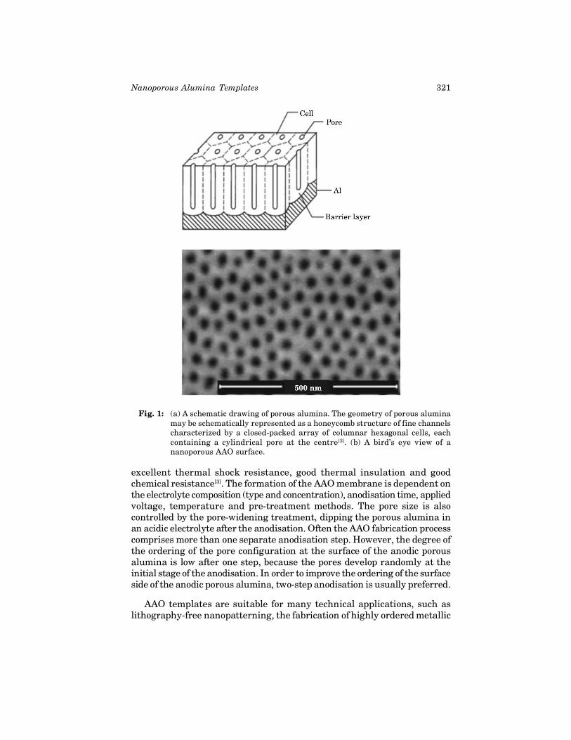
The structure of AAO, which has been found to be stable at hightemperature and in organic solvents, exhibits uniform pore density, andthe pores are parallel and perpendicular to the surface, having an idealcylindrical shape (Fig. 1(a)). A scanning electron microscopy (SEM) imageof a nanoporous AAO surface is shown in Fig. 1(b).
Every pore is embedded in a hexagonal cell structure. The cell walls aremade of Al2O3, which run parallel along the entire length of the templateand terminate at the bottom of the pores in hemispherical shells termed asthe barrier layer, which has tremendous significance in the mechanism offormation, structure and size of the AAO formed. In nanoporous AAOstructures, the pore diameter and periodicity as well as the narrowdistribution of pore size are easily controllable. Besides porosity, it shows an
321Nanoporous Alumina Templates
excellent thermal shock resistance, good thermal insulation and goodchemical resistance[3]. The formation of the AAO membrane is dependent onthe electrolyte composition (type and concentration), anodisation time, appliedvoltage, temperature and pre-treatment methods. The pore size is alsocontrolled by the pore-widening treatment, dipping the porous alumina inan acidic electrolyte after the anodisation. Often the AAO fabrication processcomprises more than one separate anodisation step. However, the degree ofthe ordering of the pore configuration at the surface of the anodic porousalumina is low after one step, because the pores develop randomly at theinitial stage of the anodisation. In order to improve the ordering of the surfaceside of the anodic porous alumina, two-step anodisation is usually preferred.
AAO templates are suitable for many technical applications, such aslithography-free nanopatterning, the fabrication of highly ordered metallic
Fig. 1: (a) A schematic drawing of porous alumina. The geometry of porous aluminamay be schematically represented as a honeycomb structure of fine channelscharacterized by a closed-packed array of columnar hexagonal cells, eachcontaining a cylindrical pore at the centre[2]. (b) A bird’s eye view of ananoporous AAO surface.
322 Nanotechnology Vol. 4: Nanomaterials and Nanostructures
nanowire arrays, the growth of carbon nanotubes or the realization ofnanocapacitor arrays. Also these templates have been frequently used forsynthesis of nanomaterials because they not only have the pores in highordering but also are reproducible and economical. Besides, it is not limitedby the choice of materials[4]. AAO can further be used as a template forfabrication of nanocomposite structures or biomaterials[5]. The advantageswhen using these templates are controllability of the pore size, ratio aspectand use of low cost, simple equipment comparing with electron beamlithography, ion beam lithography or X-ray lithography. AAO templatescan have important medical applications in drug delivery and fluidseparation. For example, in hemodialysis, a pore size that is capable ofclearing small (urea, creatinine) and middle (vancomycin, inulin) molecularweight solutes while maintaining large molecular weight molecules(albumin) is the most desirable[6]. The fabrication of ordered arrays offunctional biomolecules such as proteins, DNA, and enzymes is importantbecause of its potential for application in several kinds of biomolecularnanodevices. The use of highly ordered anodic porous alumina results inthe efficient formation of ordered arrays of biological molecules[7]. AAO canalso be used to fabricate capacitive humidity sensors because the structurehas nanosized pores, giving it a large surface area for absorbing watervapour. A thick porous layer or large pore diameter increases sensitivitybecause of increase in contact surface area[8]. Chemically functionalisedAAO membranes can be utilized for catalytic or optical purposes.Furthermore, the porous AAO membrane itself is employed for filtration,gas separation or as photonic crystals[9].
1.2. Background
Templates consisting of nanopores with uniform diameter and length areregularly used to fabricate uniform nanostructures. Fabricating suchtemplates with uniform pore diameters holds the key to controlling thesize and the shape of nanostructures[10]. Electrochemical methods have beenused to fill nanopores in the template with conducting, semiconducting orbio-molecular materials, in order to fabricate nanostructures and integratethem in circuit components[11]. Porous anodic aluminium oxides (AAO) havebeen attracting considerable attention in both scientific and commercialfields as an indispensable part of nanotechnology[12]. In 1970, O’Sullivanand Wood presented a model to describe self-regulating pore growth[13].During the anodisation process within an acidic medium, the Al surface isoxidized where the oxide layer consists of a self organized nanoporousstructure. Interest in AAO nanostructures and their fabrication using thetwo-step anodisation process has recently been reinvigorated, as describedby Masuda and Fukuda[2]. A two-step anodisation process is deemedessential in order to regulate the nanoporous structure, since irregularnanopores are formed on the Al substrate after the first anodisation.
323Nanoporous Alumina Templates
However Kirchner and co-workers fabricated AAO membranes by one-step anodisation process[14]. In their work, Al electrodes (25 mm × 10 mm)were degreased in acetone and cured for 2 h at 80ºC. The specimens wereanodised in 0.3M H2SO4 electrolyte for about 12 h at a constant potential of25.0V with a platinum cathode, at 7ºC using a stirred double jacketed vesselconnected to a thermostat. After anodisation, the remaining aluminiummetal was dissolved in a saturated iodine–methanol solution at 50ºC. Thetransparent porous anodic alumina membranes were rinsed in methanolto clean off excess iodine. Subsequently the pores on the metal contact sideof the film were opened by etching in 5% H3PO4 for 60 min at 30ºC. A three-step anodisation has also been used as a method to fabricate self-organizednanopores in oxalic and sulphuric acid. Often, the time intervals for threesteps are different. For example, Feiyue Li et al. used 5–10 mins, 0.5–12hours and 3 min for the three respective steps in their anodisation of Al[15].It was found that the order of self-assembled nanopore structures iscomparable between the three-step anodisation, and the two-stepanodisation processes. Brändli et al. used 0.3 wt% oxalic acid electrolytefor anodising Al and a wet chemical etching solution, comprising 1:1 chromicacid (0.4%) and phosphoric acid (0.6%), for selective aluminium oxidestripping[16]. The electrode was immersed in this solution for 6 min at 60°Cfor each etching step. They showed that increasing the number ofanodisation-etching cycles leads to an increase in the uniformity of thepore size and the pore diameter. However, two-step anodisation generatesan ordered pore array throughout the entire oxide layer. Well-orderednanopore arrays are obtained by etching out the oxide layer with irregularlyarranged nanopores towards the film surface. Using this two-step method,Masuda and Fukuda obtained a well ordered and hexagonal nanopore array(Fig. 1).
Formation of the pores in anodic metal oxides is described by theplasticity model where it is believed to be a consequence of flow of filmmaterial in the barrier layer region beneath the porous layer. The materialflows from the region of pore bases towards the cell wall regions due togrowth stresses and field-assisted plasticity of the film material[17-19].However, the formation mechanism of the pores is more complicated thanpreviously thought[20]. Although the formation mechanism, pore ordering,inter-pore distance and pore size control have been extensively studied,there is much work still to be done in order to understand theelectrochemistry and the anodisation process. The applied potential inanodisation varies with the type of the electrolyte used. The effect of avariety of acids has been investigated resulting in varying degrees of successas determined by the pore ordering of the arrays obtained[21]. Sulphuricacid proves to be the most commonly used acid among the more effectiveelectrolytes. When characterizing nanopore arrays, nanoindentation is atechnique providing invaluable information such as the hardness and theelastic modulus of the nanostructure investigated[22]. Xia et al. studied the
324 Nanotechnology Vol. 4: Nanomaterials and Nanostructures
effect of heat treatment on AAO showing that heat treatment up to amaximum of 600ºC leaves the elastic modulus unaffected[23].
2. ELECTROCHEMICAL PROCESS OF FABRICATING AAO
2.1. Two-Step Anodisation Method
As proposed by Masuda and Fukuda, AAO templates are produced by two-step anodisation on pre-cleaned Al substrates. The effect of pre-treatmentis discussed later in detail. The pre-cleaned Al electrodes will undergo thefirst step of the two step anodisation. Here, by applying an appropriatepotential against a Pb cathode in an acidic electrolyte, the surface of theetched Al surface is roughened to a shell-like morphology and ordered intoa hexagonal porous array. Although several acids can be used and areessential for fabricating different pore sizes, sulphuric acid is the mostcommonly used electrolyte. With sulphuric acid (H2SO4), templates withmaximum pore diameter about 40 nm can be obtained. The process usuallyis carried out in 0.3M H2SO4 at 5ºC and by applying 40V anodisationpotential. The divots formed in pores on the AAO structure is then etchedout in a chromophosphoric solution (H3PO4 8% vol + Cr2O3 4% wt). Thebase of the divots will initiate new pore formation and thus the Al substrateis ready for a second anodisation, the templating process that results inthe highly ordered nanoporous structure. This step is similar in terms ofanodisation conditions such as the applied potential, temperature andconcentration of acid but different in duration of the anodisation. Theduration of the first anodisation is generally about 1hour whereas that ofthe second anodisation varies from 2 to 7 hours depending on the desiredpore size.
2.2. Current Density and Pore Formation
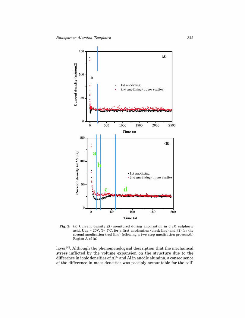
A typical current density plot during the anodisation of Al foils (99% purity)in 0.3 M H2SO4 acid is shown in Fig. 2, which consists of three noticeablecurrent density regions for the formation of porous alumina.
At the initial stage (region A), a barrier layer is first formed on thealuminium surface when the potential is applied[24]. With the growth of theoxide barrier layer through the relatively fast reaction at the very earlystages of the process, the resistance of the electrode increases resulting ina sharp decrease in current density, as shown in the region ‘a’ of the inset.With this process, transport of Al3+ ions and their ejection to electrolyteresults in a slow increase in the current density (region ‘b’). However, steadycurrent density is observed as shown in region ‘d’, when equilibrium isachieved between the AAO formation and the Al3+ ion ejection (‘c’ and ‘d’).Singh et al. attributed the pore initiation and self organization of the porousstructures at the initial stage to the considerable elastic stress in the oxide
325Nanoporous Alumina Templates
Fig. 2: (a) Current density j(t) monitored during anodisation in 0.3M sulphuricacid, Uap = 20V, T= 5ºC, for a first anodisation (black line) and j(t) for thesecond anodisation (red line) following a two-step anodisation process.(b)Region A of (a)
layer[25]. Although the phenomenological description that the mechanicalstress inflicted by the volume expansion on the structure due to thedifference in ionic densities of Al3+ and Al in anodic alumina, a consequenceof the difference in mass densities was possibly accountable for the self-
326 Nanotechnology Vol. 4: Nanomaterials and Nanostructures
organized formation of hexagonal pore arrays (Fig. 1)[26]. Hence the poreformation and the porous film growth is better described using the “Plasticionic flow model”, where the pore formation in the anodized oxide isexplained in terms of mass migration of metal ions within the oxide fromunderneath the pores to pore wall. As described in the literature, barrier-type anodic alumina films grow by migration of Al3+ ions outward and O2"
ions inward[27]. As Thompson described, about 40% of the film thicknessforms at the AAO film/electrolyte interface as a result of the migration ofAl3+ ions for growth at 100% efficiency. The remainder of the film thicknessis formed at the metal/film interface by migration of O2" ions[28]. Theformation of the porous film takes place when there is no film materialbeing added at the Al2O3/electrolyte interface. According to Thompson etal, this corresponds to an efficiency of about 60% for conditions close tothose presently used for anodisation. Whilst increased stresses fromelectrostriction assist stabilization of the pores, the absence of growth ofnew oxide at the film surface prevents pore-filling.
Although in general the current densities of the first and the secondanodisation demonstrate similar overall behaviour over time, certaindifferences have also been observed. The lowest apparent current densityis generally higher for the second anodisation step than for the first andthe time taken to reach the constant current density during the secondanodisation is shorter than that in the first step. This irregularity can beattributed to the fact that in the first anodisation step the porous structureis not yet formed, while in the second anodisation, the patterning of thepores has already taken place, after removing the aluminium oxide layerby etching in chromophosphoric acid solution (H3PO4 and H2CrO4).
2.3. Chemical Reactions
The reactions during anodisation under steady state conditions take placeacross the barrier layer. Reactions related to formation of pores occur atboth the Al/Al2O3 interface and the Al2O3/electrolyte interface through ionmigration across the barrier layer. As has been reported previously, thedissociation of water supplies anions to the oxide layer, but also plays animportant role in governing the porosity of the porous AAO films[29]. Whilethe anions, O2- or OH- ions, drift towards the Al/Al2O3 interface, Al3+ ionsdrift towards the Al2O3/electrolyte interface. Eventually Al3+ ions are ejectedinto the electrolyte, which results in the dissolution of Al2O3 (Equation 1a).
Al2O3 + 6H+ 2Al3+(aq) + 3H2O (1a)
In the meantime, reaction between Al and the anion produced by watercontinues to produce Al2O3 (Equation 1b).
2Al + 3H2O Al2O3 + 6H+ + 6e- (1b)
327Nanoporous Alumina Templates
The dynamic equilibrium between the two reactions at steady statefacilitates self assembly of the porous AAO structure.
2.4. Mechanism of Self-Assembly of Nanopores
According to the phenomenological model, self-assembly and ordering is aresult of the mechanical stress associated with the volume expansion duringthe oxide formation on Al since simultaneous growth of pores restricts Al2O3to growing perpendicular to the Al surface. The porous structure self-ordersunder steady state, when the mechanical stress generated between thepore walls is equilibrated.
Among the other models proposed to describe the mechanism of self-assembly, the simple electrostatic model of the field-assisted dissolution ofthe barrier layer or the plasticity model has been widely accepted[30].According to the model, the electric field at the Al2O3/electrolyte interfaceresponds to any change in pore sizes during anodisation. The electric fieldincreases whenever the pore diameter decreases from its equilibrium value,increasing the field assisted dissolution rate, which eventually will causethe pore diameter to increase. The self-assembly of the pore structure isgoverned by electric field changes to the pore surface morphology, whichcounteract any physical changes. The film material in the barrier layerregion beneath the porous layer will flow from the region of pore basestowards the cell wall regions due to growth stresses and field-assistedplasticity of the film material.
2.5. The Effect of the Electrolyte and Supporting Evidence
The two-step anodisation process is commonly used to fabricate AAO withdifferent types of electrolyte such as sulphuric acid, oxalic acid andphosphoric acid. For each electrolyte, one has to choose applied voltage,temperature of electrolyte, time of anodisation and concentration of acid toget optimized pores. This restriction in choice of conditions for anodisationis due to the conductivity and pH value of the electrolyte. For example, ifaluminium is anodized in sulphuric acid at a relatively high potential (notethat sulphuric acid has a very high conductivity), the oxide layer breaksdown easily. In addition, the pH-value of the electrolyte determines thesize of the pores. The lower the pH value, the lower the potential thresholdfor field-enhanced dissolution at the pore tip, which leads to a smaller poresizes. Therefore, large pore diameters are formed by using the oxalic orphosphoric acid and small pore diameters are obtained by using sulphuricacid.
For example, Xin Wang et al. worked with 0.3M oxalic acid, and theapplied voltage was 30-50 V at room temperature[31]. The results showdistinctly an ordered honeycomb structure with uniform pore-diameter and
328 Nanotechnology Vol. 4: Nanomaterials and Nanostructures
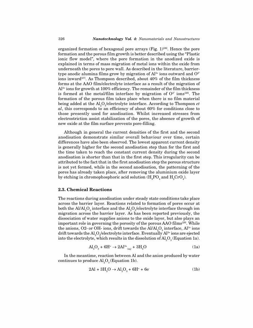
inter pore-spacing fabricated with this method. The pore diameter was 20nm and pore spacing was 80 nm for AAO when 40 V was applied, while theapplication of 50 V caused pore-size to be 35 nm in diameter and 110 nm inspacing. A. Belwalkar et al. used 2.7 wt% oxalic acid and anodised Al underdifferent voltages at 0ºC[32]. The pore diameter and the interpore distancewere 18.6 ± 2.9 and 65.1 ± 6.5 respectively under an applied potential of30V whereas they were 33.6 ± 7.6 and 80.5 ± 3.2, respectively under 40Vapplied potential. Although pores with smaller diameter (~18 nm) can bemade with oxalic acid, significantly large pore sizes can also be made. Incontrast, Fig. 3 shows (a) an SEM image and (b) an atomic force microscopy(AFM) image of an AAO template surface after the two anodisation stepsin 0.3M sulphuric acid. Templates with nanopores of a uniform size exhibitan almost perfect 2-D array with a hexagonal pattern. The average diameterand interpore distance are 26 ± 1 and 42 ± 2 nm, respectively, which arethe highest dimensions that can be achieved when using sulphuric acid.Here, the pore density is about 2.7 × 10¹⁰ pores/cm2.
C.T. Sousa et al. investigated nanoporous self-organized AAO templates,where both the anodisation steps were carried out in 0.3M H2SO4 at voltages15V, 20V and 25V, for 2h, at temperature 12 ± 2ºC[33]. The results of thisresearch are an applied potential of 25V giving the best conditions for theappearance of organized patterns. There is a confinement of pore order tothe aluminium grains. The anodisation at 25V gave the largest interporedistance in the aluminium (~30 nm).
Jaime Martín et al. used a phosphoric acid/methanol/water mixture(1:10:89, weight proportions) electrolyte, and anodised under a constantpotential of 195V and at -4ºC (methanol was added to the electrochemical
Fig. 3: SEM images of the surface of AAO templates (a) after the second anodization,and (b) after pore widening
329Nanoporous Alumina Templates
bath in order to avoid the electrolyte from freezing)[34]. To avoid completelythe breakdown, the voltage at the beginning was 185V and increased to195V after 4h. The first anodic layer was then removed by chemical etchingin a mixture of phosphoric acid (7 wt.%) and chromic oxide (1.8 wt.%).Finally, the second anodisation was performed in the same conditions asthe first, but directly under 195V. The results were pore diameter 137nmand interpore distance 447 nm.
Leszek Zaraska et al. also fabricated AAO templates by a two-step processunder a constant voltage (110, 160, 170 V) in a 0.3 M H3PO4 electrolyte or analcohol at the temperature of 0 or “5 ± 0.02°C[35]. The duration of eachanodisation step was 8 h. The alumina layer formed during the first step ofanodisation was removed by chemical etching in a mixture of 6 wt% H3PO4and 1.8 wt.% H2CrO4 at 60°C for 2 h. After the oxide removal, the secondanodisation was performed under the same conditions as in the first step.The anodisation potential had no effect on the pore circularity for samplesmade in 0.3 M H3PO4 electrolyte while the complex pore structure with sub-pores were formed underneath the film surface. However, the regularity ofpore arrangement and uniformity of pore structure increased with thepotential, independent of the electrolyte composition. The interpore distanceof pore structure of AAO films increased from 342 nm to 478 nm whenanodisation potential was increased from 110 V to 160 V. Younghee Na etal. however used a different approach, where they used two differentelectrolytes for the two steps of anodisation, namely 0.2 M phosphoric acidin the first anodisation and 0.2 M oxalic acid in the second anodisation step[36].The synthesized AAO templates could be successfully used to obtain highlyordered nanometer-sized wires for large area device applications.
Electrolytes such as citric acid, chromic acid and tartaric acid, have alsobeen used with varying success elsewhere[37]. In summary, the relationshipbetween the conditions for fabrication AAO templates in commonelectrolytes are given in Table 1.
Table 1: Structural features of nanostructure obtained by anodizing in variousconditions
Electrolyte Voltage Pore diameter Inter-pore(V) (nm) distance (nm)
Phosphoric acid (H3PO4) 100-195 130-250 250-500
Oxalic acid (H2C2O4) 30-80 40-100 80-200
Sulphuric acid (H2SO4) 15-25 15-25 60-70
2.6. The Effect of Pre-Treatment
The quality of surface of substrates has major influences on thenanostructure by self-organized anodisation. The surface of the alumina
330 Nanotechnology Vol. 4: Nanomaterials and Nanostructures
film can be modified thermally or by electrochemical and chemical pre-treatment. The pre-treatment process accelerates the reduction in surfacedefects. Fratila-Apachitei et al. investigated the influence of substratemicrostructure on the growth of anodic oxide layer, the results of whichshowed that the uniformity of the oxide growth increased with theincreasing purity of aluminium[38].
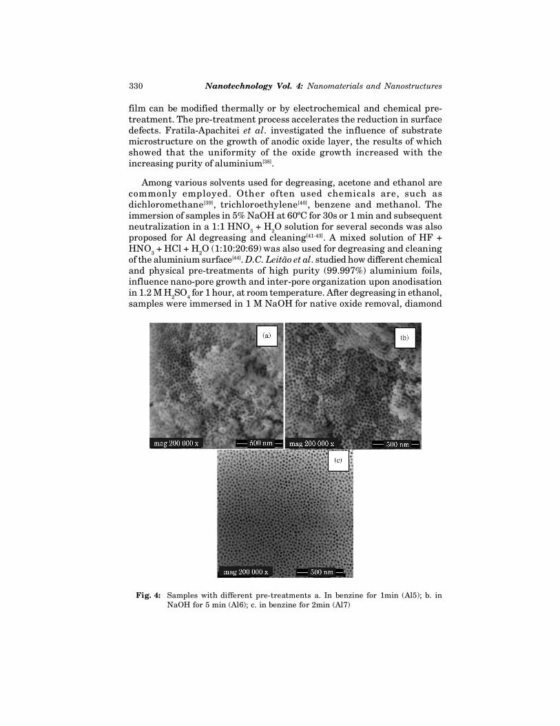
Among various solvents used for degreasing, acetone and ethanol arecommonly employed. Other often used chemicals are, such asdichloromethane[39], trichloroethylene[40], benzene and methanol. Theimmersion of samples in 5% NaOH at 60ºC for 30s or 1 min and subsequentneutralization in a 1:1 HNO3 + H2O solution for several seconds was alsoproposed for Al degreasing and cleaning[41-43]. A mixed solution of HF +HNO3 + HCl + H2O (1:10:20:69) was also used for degreasing and cleaningof the aluminium surface[44]. D.C. Leitão et al. studied how different chemicaland physical pre-treatments of high purity (99.997%) aluminium foils,influence nano-pore growth and inter-pore organization upon anodisationin 1.2 M H2SO4 for 1 hour, at room temperature. After degreasing in ethanol,samples were immersed in 1 M NaOH for native oxide removal, diamond
Fig. 4: Samples with different pre-treatments a. In benzine for 1min (Al5); b. inNaOH for 5 min (Al6); c. in benzine for 2min (Al7)
331Nanoporous Alumina Templates
paste polished, electropolished and ion-milled. They obtained that thesmoothness of Al-foil surface is crucial in order to get a good quality porousstructure. Pre-treatment with NaOH etching gives the best results for goodquality and, to a certain extent, organised pore structures[45].
Fig. 3 shows three samples following different pre-treatment processes.In the two samples treated in benzine for 1min and NaOH for 5 min (Al6),the physical parameters of the AAO are similar. However, the morphologyof the surface is uneven; the pores can be seen at different levels. In contrast,in the sample etched in benzine for 2 min (Al7), the surface is found to bemore uniform.
2.7. Pore Size Analysis
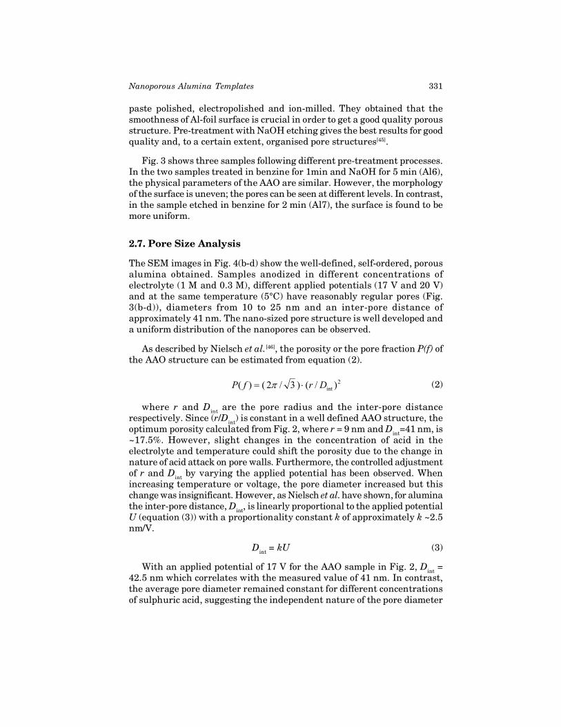
The SEM images in Fig. 4(b-d) show the well-defined, self-ordered, porousalumina obtained. Samples anodized in different concentrations ofelectrolyte (1 M and 0.3 M), different applied potentials (17 V and 20 V)and at the same temperature (5°C) have reasonably regular pores (Fig.3(b-d)), diameters from 10 to 25 nm and an inter-pore distance ofapproximately 41 nm. The nano-sized pore structure is well developed anda uniform distribution of the nanopores can be observed.
As described by Nielsch et al.[46], the porosity or the pore fraction P(f) ofthe AAO structure can be estimated from equation (2).
2int )/()3/2()( DrfP (2)
where r and Dint are the pore radius and the inter-pore distancerespectively. Since (r/Dint) is constant in a well defined AAO structure, theoptimum porosity calculated from Fig. 2, where r = 9 nm and Dint=41 nm, is~17.5%. However, slight changes in the concentration of acid in theelectrolyte and temperature could shift the porosity due to the change innature of acid attack on pore walls. Furthermore, the controlled adjustmentof r and Dint by varying the applied potential has been observed. Whenincreasing temperature or voltage, the pore diameter increased but thischange was insignificant. However, as Nielsch et al. have shown, for aluminathe inter-pore distance, Dint, is linearly proportional to the applied potentialU (equation (3)) with a proportionality constant k of approximately k ~2.5nm/V.
Dint = kU (3)
With an applied potential of 17 V for the AAO sample in Fig. 2, Dint =42.5 nm which correlates with the measured value of 41 nm. In contrast,the average pore diameter remained constant for different concentrationsof sulphuric acid, suggesting the independent nature of the pore diameter
332 Nanotechnology Vol. 4: Nanomaterials and Nanostructures
from the acid concentration. As Masuda and Fukuda first reported, self-organized pore growth leads to a densely packed hexagonal pore structurefor certain sets of parameters, as illustrated in Fig. 4(a).
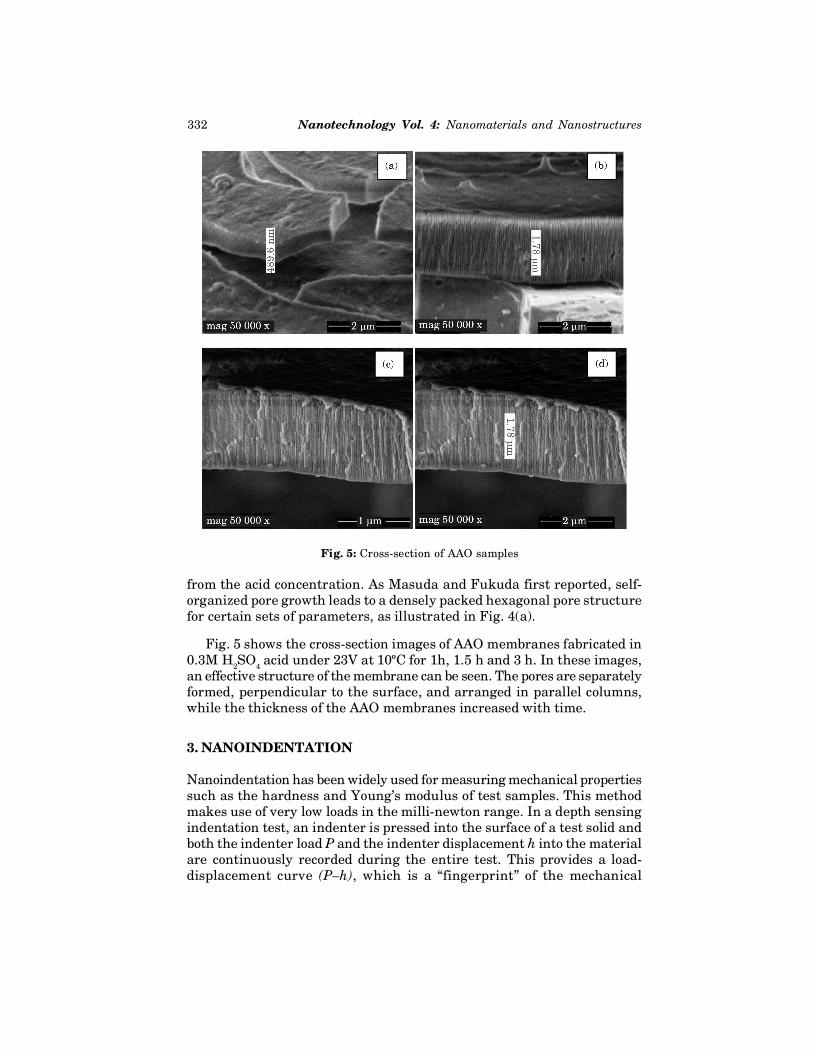
Fig. 5 shows the cross-section images of AAO membranes fabricated in0.3M H2SO4 acid under 23V at 10ºC for 1h, 1.5 h and 3 h. In these images,an effective structure of the membrane can be seen. The pores are separatelyformed, perpendicular to the surface, and arranged in parallel columns,while the thickness of the AAO membranes increased with time.
3. NANOINDENTATION
Nanoindentation has been widely used for measuring mechanical propertiessuch as the hardness and Young’s modulus of test samples. This methodmakes use of very low loads in the milli-newton range. In a depth sensingindentation test, an indenter is pressed into the surface of a test solid andboth the indenter load P and the indenter displacement h into the materialare continuously recorded during the entire test. This provides a load-displacement curve (P–h), which is a “fingerprint” of the mechanical
Fig. 5: Cross-section of AAO samples
333Nanoporous Alumina Templates
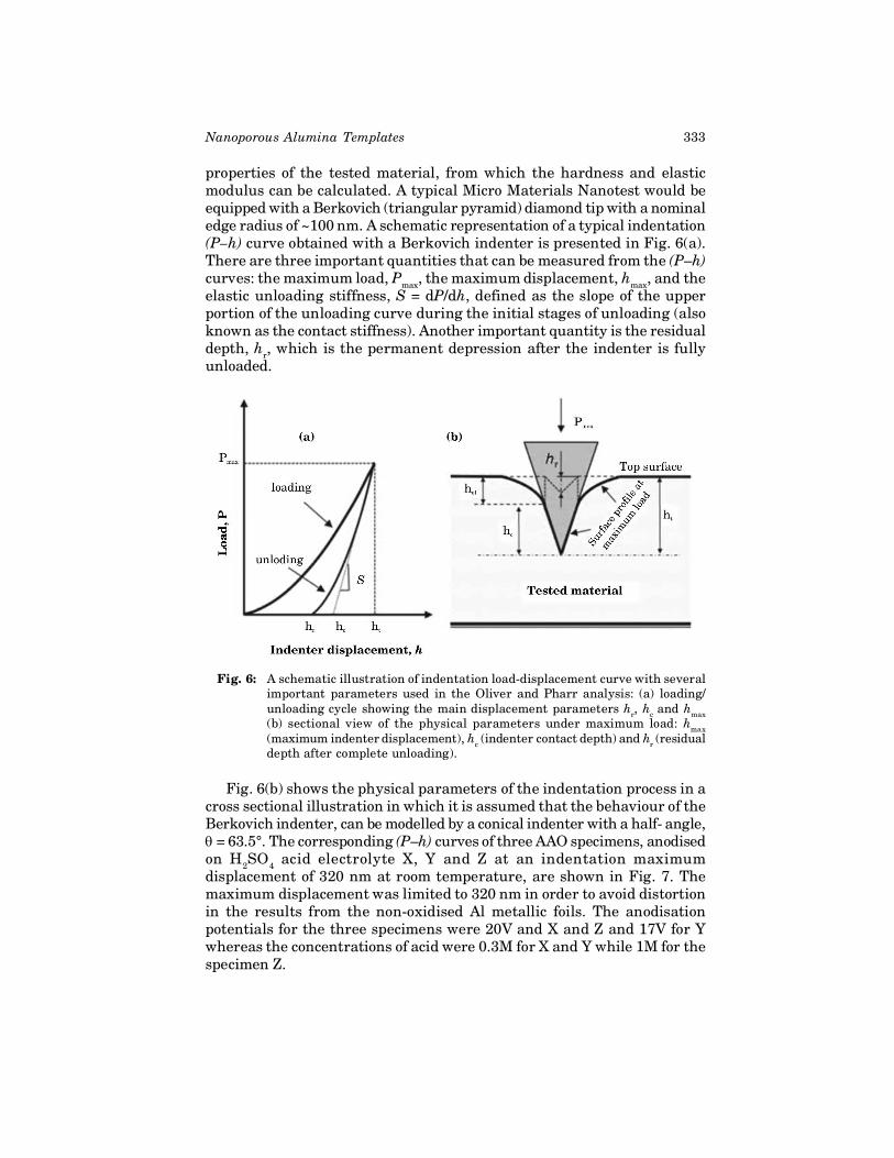
properties of the tested material, from which the hardness and elasticmodulus can be calculated. A typical Micro Materials Nanotest would beequipped with a Berkovich (triangular pyramid) diamond tip with a nominaledge radius of ~100 nm. A schematic representation of a typical indentation(P–h) curve obtained with a Berkovich indenter is presented in Fig. 6(a).There are three important quantities that can be measured from the (P–h)curves: the maximum load, Pmax, the maximum displacement, hmax, and theelastic unloading stiffness, S = dP/dh, defined as the slope of the upperportion of the unloading curve during the initial stages of unloading (alsoknown as the contact stiffness). Another important quantity is the residualdepth, hr, which is the permanent depression after the indenter is fullyunloaded.
Fig. 6: A schematic illustration of indentation load-displacement curve with severalimportant parameters used in the Oliver and Pharr analysis: (a) loading/unloading cycle showing the main displacement parameters hr, hc and hmax(b) sectional view of the physical parameters under maximum load: hmax(maximum indenter displacement), hc (indenter contact depth) and hr (residualdepth after complete unloading).
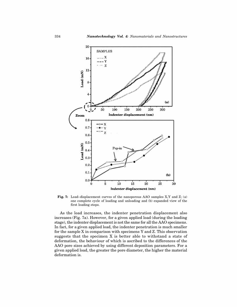
Fig. 6(b) shows the physical parameters of the indentation process in across sectional illustration in which it is assumed that the behaviour of theBerkovich indenter, can be modelled by a conical indenter with a half- angle, = 63.5°. The corresponding (P–h) curves of three AAO specimens, anodisedon H2SO4 acid electrolyte X, Y and Z at an indentation maximumdisplacement of 320 nm at room temperature, are shown in Fig. 7. Themaximum displacement was limited to 320 nm in order to avoid distortionin the results from the non-oxidised Al metallic foils. The anodisationpotentials for the three specimens were 20V and X and Z and 17V for Ywhereas the concentrations of acid were 0.3M for X and Y while 1M for thespecimen Z.
334 Nanotechnology Vol. 4: Nanomaterials and Nanostructures
As the load increases, the indenter penetration displacement alsoincreases (Fig. 7a). However, for a given applied load (during the loadingstage), the indenter displacement is not the same for all the AAO specimens.In fact, for a given applied load, the indenter penetration is much smallerfor the sample X in comparison with specimens Y and Z. This observationsuggests that the specimen X is better able to withstand a state ofdeformation, the behaviour of which is ascribed to the differences of theAAO pore sizes achieved by using different deposition parameters. For agiven applied load, the greater the pore diameter, the higher the materialdeformation is.
Fig. 7: Load–displacement curves of the nanoporous AAO samples X,Y and Z; (a)one complete cycle of loading and unloading and (b) expanded view of thefirst loading steps.
335Nanoporous Alumina Templates
In addition, as shown in Fig. 7b, the pop-in behaviour occurs at thebeginning of the loading process. This behaviour, as Fang et al. described,(which is different from the dislocation-slip phenomenon) is due to thenanopore walls crashing one with another[47]. Although the indenter size isgreater than the average pore or cell size, in the early stages of the appliedload, the surface contact area between the indenter and the AAO materialshould be very small, which makes the average contact pressure higherthan that of the rupture strength of the material, leading to the materialcollapse. Furthermore, the indentation results can be used to characterizethe mechanical properties of the AAO samples by estimating the hardnessand the Young’s modulus of the specimens. The hardness H is the pressureexerted by the indenter at the maximum load Pmax on the material, thus itis determined from the equation
A
PH max (4)
where A is the projected (or cross sectional) area of the indenter at adistance hc back from its tip. The distance hc is the depth along which contactis made between the indenter and the specimen. Under full load, theindenter is impressed to a total (maximum) depth hmax, which can be takenfrom the load-displacement curve as indicated in the Fig. 6(a) and (b). Afterunloading is complete, there remains a residual depression of depth hr,which is also given in the load-displacement curve.
Since the hardness defined to be based on the projected contact areaunder load, it may not be as same as the conventional hardness (measured
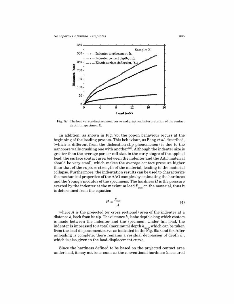
Fig. 8: The load versus displacement curve and graphical interpretation of the contactdepth in specimen X.
Sample: X
336 Nanotechnology Vol. 4: Nanomaterials and Nanostructures
from the surface area of the residual hardness impression), if there issignificant elastic recovery during unloading. The elastic modulus relatesto contact area and the measured unloading stiffness[48] through theequation (5).
(5)
where Er, the ‘reduced elastic modulus’ (or the effective elastic modulus)can be given by:
(6)
The reduced elastic modulus takes into account the fact that elasticdisplacements occur in both the specimen and the indenter. The Young’smodulus and the Poisson’s ratio of the specimen and the indenter E,v andEi, vi respectively. The properties of the diamond indenter used are Ei =1140 GPa and íi = 0.07[49] and the Poisson’s ratio of the AAO specimens is0.22[22].
Fig. 9: Hardness as a function of the indenter depth.
The equation (5) is a general relation that applies to any axisymmetricindenter, where the dimensionless parameter, , is used to account fordeviations in stiffness caused by the lack of axial symmetry for pyramidalindenters[50,51]. Indentation experiments are often conducted with non-axisymmetric indenters, King used finite element simulations to estimatevalues for different indenter geometries[52]. He found that = 1.034 for atriangular punch, the value which has been widely adopted for instrumentedindentation testing with a Berkovich indenter.
337Nanoporous Alumina Templates
Although the equations (5) and (6) have been used for isotropic materialsand a partial effect from other directions exists in the transversely isotropiccase, it is still possible to apply the equations to estimate the elastic constantin the indentation direction.The analysis used to determine the hardness,H, and elastic modulus, E, is an extension of the method proposed by Doernerand Nix that accounts for the fact that unloading curves are distinctly curvedin a way that cannot be explained by the flat punch approximation[53].Generally, in the flat punch approximation, the contact area remainsconstant as the indenter is removed, and the resulting unloading curve islinear. In contrast, experiments performed by Oliver and Pharr have shownthat unloading curves are distinctly curved and usually well fitted by aspecific power law[54]. The procedure used to measure H and E, followingthe work performed by Oliver and Pharr, is based on the unloading processshown schematically in Fig. 6(a), in which the elastic deflection, hel, of thesample surface at the maximum load is given by:
(7)
where is a constant that depends on the geometry of the indenter andtakes the numerical values of 1.00 for a flat punch, = 0.72 for a conicalpunch, and = 0.75 for a Berkovich indenter .
From the geometry of Fig. 6(b) that the depth along which, the contactis made between the indenter and the specimen, hc = hmax – hel, is:
(8)
In order to determine the hardness of a material, equation (4) should beused. However, since the definition of ardness is based on the projectedcontact area under load, Oliver and Pharr have defined an “area function”,F(hc) that describes the projected (or cross sectional) area of the indenterat a distance, hc, back from its tip. The area function is given by a multi-term polynomial fit of the form:
(9)
For a perfect pyramid or cone the area function can be represented bythe first term alone. By assigning the constant C0 associated with thequadratic term to a value determined by the face angles of a Berkovichpyramid (with a half- angle of 65.3°), the resulting contact area is given by:
(10)
338 Nanotechnology Vol. 4: Nanomaterials and Nanostructures
Mean while, the monitoring of the average contact pressure is difficultdue to the fact that the indenter displacement, rather than the contactdepth, is measured during a nanoindentation test. The indenterdisplacement is the sum of the contact depth and the elastic deflection ofthe sample surface at the contact edge. It is therefore necessary to subtractthe elastic deflection from each displacement measurement in order tocalculate the average contact pressure. Oliver and Pharr technique, whichis most often used to manipulate the nanoindentation test results, onlyprovides the elastic deflection at the peak load. Thus, the proceduresuggested by Novikov et al.[55] and Carneiro et al.[56] is used to monitor theaverage contact pressure during reloading of the indenter. The currentactual value for the elastic deflection h(el)i of the sample surface at contactperimeter can be obtained as:
(hel )i hel (Pi / Pmax )1/2 (11)
where Pi is the actual value of the applied load. The load dependenceover the contact depth is found by subtracting the actual elastic deflection(calculated uing using equation (11)) from the actual displacement data,according to the following equation
ieliic hhh )()( (12)
where (hc)i is the actual contact depth and hi the actual displacement ateach indentation reloading point.
Mean while, the dependence of contact depth as well as the materialsurface elastic deflection over the applied load (under the loading process),is revealed in Fig. 8. The surface elastic deflection of the tested specimenincreases slowly with the indenter displacement. However, for the sameapplied load, the magnitude of the contact depth is much more pronounced.In fact, at the peak load, the elastic deflection represents only 25% of contactdepth. It can be noted that for an applied load smaller than 2.5 mN, thecontact depth increases rapidly as a result of the crash of nanopore walls.
Hardness as a continuous function of penetration depth can be calculatedin two steps. First, the elastic deflection of the sample surface at the peakload hel has to be established using the Oliver and Pharr method. Thenequation (12) can be substituted in equation (4) in order to calculate theactual hardness, Hi (see Fig. 8). The hardness values are obtained from allloading curve data points and correspond to the ratio between the actualapplied loads and actual projected contact areas:
2-2/1maxmax ])/()/([
56.24)( PPSPh
PH ii
ii (13)
339Nanoporous Alumina Templates
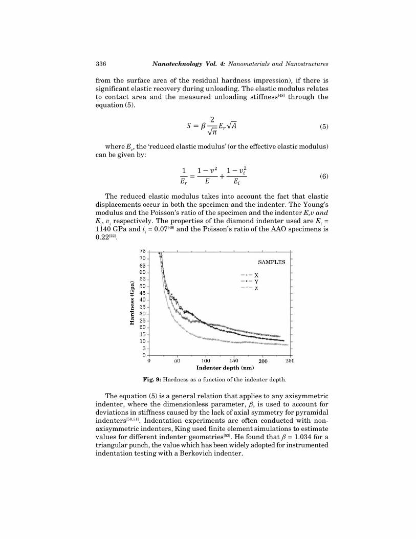
For the three specimens considered in this section, as demonstrated inFig. 9, two regions can be highlighted on the hardness dependence overthe indenter depth. In the first region, at a depth up to 75 nm, a significantdecrease in hardness is observed. The hardness decreased from 75 GPa ata depth of ~ 20 nm to ~25 GPa for specimens X and Y and to ~ 15 GPa forspecimen Z. However, from ~ 75 nm to 245 nm, the hardness decreasesslowly with the indenter depth. Such behaviour in hardness suggests thatthese measurements should be made (ideally) using sharp indenters.
Since real pyramid indenters (such as Berkovich indenter) have a smallrounded imperfection on its tip (inevitably occurs during its grindingprocess), for accurate measurements of hardness, the contact area betweenthe indenter and the test material should be much larger when comparedwith the area of the defect at the indenter tip. This requirement is easy toattain for soft materials such as metals. However, for hard materials (oxides,carbides, nitrides etc.) at the beginning of an indentation experiment whenthe applied load is very low, the area of the defect at the indenter tip caneventually be comparable to contact area. Under this condition, it is expectedthat small tip-rounded indenters can have some influence on hardnesscalculations, since it can lead to the estimation of hardness with highmagnitudes. For the tested AAO specimens, it was observed that thehardness increases substantially for loads lower than approximately 2 mN.Meanwhile, as the contact depth increases, the contact area between theindenter and the tested AAO material would surpasses the size of defectsat the indenter tip reducing the hardness. This behaviour could also be aresult of the fragile and porous structure of the AAO film, where the indenterpenetrates the material; it is cracked to interior layers below the indentertip. On the other hand, for the region between ~7 nm to 245 nm, the hardnessremains almost constant despite the increase in indenter depth, thereforepartly reflecting the mechanical properties of the crushed oxide. The porousstructure of the AAO should lead to a deformation mechanism via crushedpores although the solid barrier layer may partially alleviate the crushedpores underneath the indenter. Moreover, for the region corresponding tothe greater indenter penetration depths, the very steady hardness valuessuggest that the effect from the contribution of the substrate is not detectedsince the penetration depth is much lower than that of the film thickness.Fig. 9 also shows that the highest hardness value, calculated for maximumindenter penetration depth, was recorded for the sample prepared underthe largest applied voltage.
The hardness, H, and Young’s modulus, E of the AAO samples are givenin Table 2. The hardness of the sample X is higher than that the sample Zand Y. This can be explained by the morphology of the surface of thesamples, as previously mentioned.
The Young’s moduli of the three nanoporous AAO samples, calculatedfor the highest indentation depth (of about 245 nm), are 131.2 GPa, 192.4
340 Nanotechnology Vol. 4: Nanomaterials and Nanostructures
GPa and 163.2 GPa, respectively. The Young’s moduli obtained here areabout 15% higher than those found elsewhere[57], primarily because theaverage pore diameter is smaller in this work than other studies.Additionally, the values of the Young’s modulus herein obtained may alsobe associated with either absorbed moisture or residual water from theanodisation process, or the exposure to air.
4. CONCLUSIONS
Well-defined, self-ordered, porous alumina structures can be obtained bytwo-step electrochemical anodisation of Al electrodes in several electrolytes.Pores with smaller dimensions are obtained with sulphuric acid whilephosphoric or oxalic acids produce pores with larger dimensions. Bothanodisation time and applied potential affect the regularity and size of thenanopores, although the effect of the potential appears to be stronger thanthe effect of temperature in the transformation from crystalline aluminato amorphous alumina. While the inter-pore distance is linearly proportionalto the applied potential, pore diameter remained independent of the acidconcentration. Optimum pore growth was achieved with a pore fraction,P(f)~17.5%. This experimental pore fraction probably needs furtheroptimising for improved pore ordering.
Where the mechanical properties of AAO structures are investigatedusing nanoindentation, the smallest pore diameter produces the highesthardness value. The analysis of the hardness–contact depth data revealsthat the indentation hardness decreases in inverse proportion to theindenter penetration depth. Furthermore, the corresponding hardnessremains constant despite the increase in indenter depth.
5. ACKNOWLEDGEMENTS
The authors would like to thank the FCT (Fundação para a Ciência eTecnologia) for funding through the Ciencia 2007 programme and thepluriannual contract with CFUM and the European Commission throughFP7-PEOPLE-2010-IRSES-NanoCIS (269279) project.
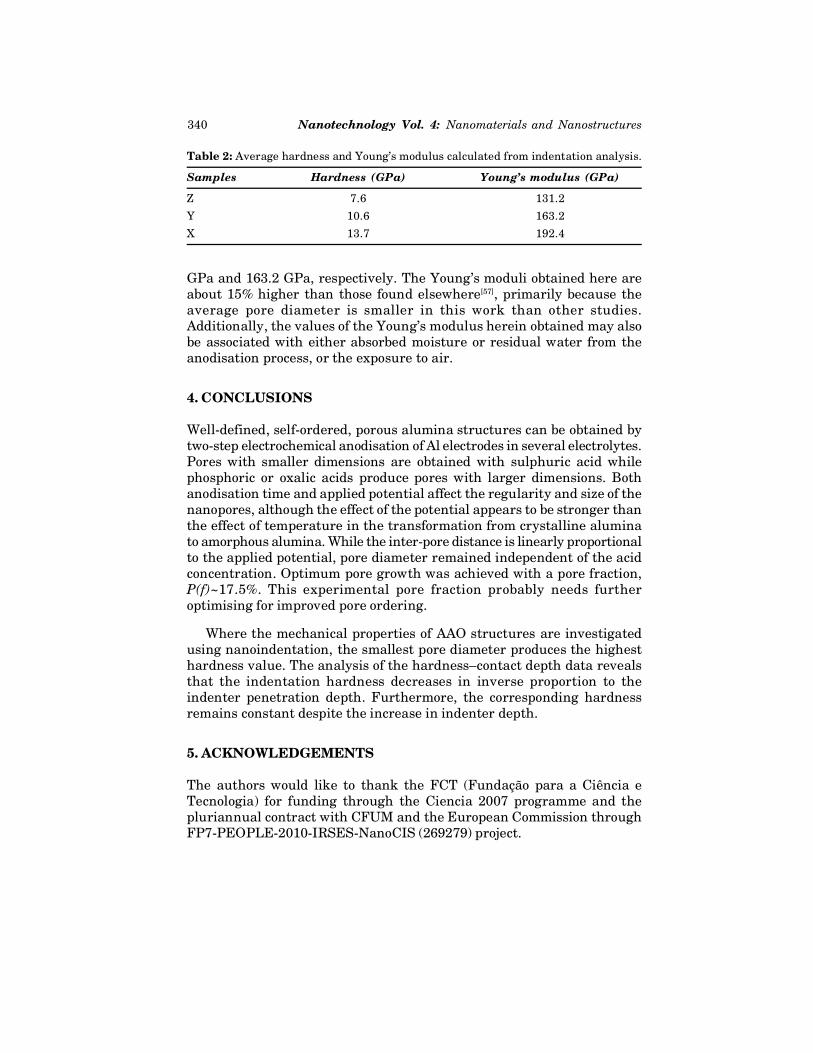
Table 2: Average hardness and Young’s modulus calculated from indentation analysis.
Samples Hardness (GPa) Young’s modulus (GPa)
Z 7.6 131.2
Y 10.6 163.2
X 13.7 192.4
341Nanoporous Alumina Templates
REFERENCES
[1] Thompson, D.W., Snyder, P.G., Castro, L., Yan, L., Kaipa, P. and Woollam, J.A.(2005). J. App. Phys., 97: 113511–113519.
[2] Masuda, H. and Fukuda, K. (1995). Science, 268: 1466–1468.[3] Son, H.Le., Angela, Camerlingo. and Hoa, T.M., Pham2, Behzad Rejaei1, Pasqualina
M. Sarro, Anodic Aluminum Oxide Templates for Nanocapacitor Array Fabrication,[email protected].
[4] Kwang Hong, Lee., Yuan Peng, Huang. and Chee Cheong, Wong. (2011).Electrochimica Acta, 56: 2394–239.
[5] Hideki, Masuda. and Kazuyuki, Nishio. (2006). Nanostructure Science andTechnology, pp. 296–312
[6] Belwalkar, A., Grasing, E., Van Geertruyden, W., Huang, Z. and Misiolek, W.Z.(2008). Journal of Membrane Science, 319: 192–198.
[7] Hideki, Masuda. and Kazuyuki, Nishio. (2006). Nanostructure Science andTechnology, pp. 296–312.
[8] Youngdeuk, Kim., Bongbu, Jung., Hunkee, Lee., Hyejin, Kim., Kunhong, Lee. andHyunchul, Park. (2009). Sensors and Actuators B, 141: 441–446.
[9] Thompson, D.W., Snyder, P.G., Castro, L., Yan, L., Kaipa, P. and Woollam, J.A.(2005). J. App. Phys., 97: 113511–113519.
[10] Aricò, A.S., Bruce, P., Scrosati, B., Tarascon, J.M. and Schalkwijk, W.V. (2005).Nature Mater, 4: 366–377.
[11] Moon, J.M. and Wei, A. (2005). J. Phys. Chem. B, 109(49): 23336–23341.[12] Dickson, R.M. and Lyon, L.A. (2000). J. Phys. Chem. B, 104: 6095–6098.[13] O’Sullivan, J.P. and Wood, G.C. (1970). Proc. R Soc. A, 317: 511–543.[14] Kirchner, A., MacKenzie, K.J.D., Brown, I.W.M., Kemmitt, T. and Bowden, M.E.
(2007). Journal of Membrane Science, 287: 264–270.[15] Feiyue, Li., Lan, Zhang. and Metzger Robert, M. (1998). Chem. Mater, 10:
2470–2480.[16] Christof, Brandli., Jaramillo Thomas, F., Anna, Ivanovskaya. and McFarland Eric,
W. (2001). Electrochimica Acta, 47: 553–557.[17] Patermarakis, G. and Moussoutzanis, K. (2011). J. Electroanal. Chem., 659:
176–190.[18] Garcia-Vergara, S.J., Skeldon, P., Thompson, G.E. and Habazaki, H. (2006).
Electrochim. Acta, 52: 681.[19] Garcia-Vergara, S.J., Skeldon, P., Thompson, G.E. and Habazaki, H. (2007). Surf.
Coat. Technol., 201: 9506.[20] Cheng, Chuan. and Ngan, A.H.W. (2011). Electrochimica Acta, 56: 9998–10008.[21] Sadasivan, V., Richter, C.P., Menon, L. and Williams, P.F. (2005). AIChE Journal,
51(2): 649–655.[22] Fang, T.H. and Chang, W.J. (2003). Microelectron Eng., 65: 231–238.[23] Xia, Z., Riester, L., Sheldon, W., Curtin, W.A., Liang, J., Yin, A. and Xu, J.M.
(2004). Rev. Adv. Mater Sci., 6: 131–139.[24] Zhao, X., Seo, S.K., Lee, U.J. and Lee, K.H. (2007). J. Electrochem. Soc., 154(10):
C553–C557.[25] Singh, G.K., Golovin, A.A. and Aranson, I.S. (2006). Phys. Rev. B, 73(20): 205422-
1-205422-12[26] Jessensky, O., Muller, F.d and Gosele, U. (1998). Appl. Phys. Lett., 72(10): 1173–
1175.[27] Brown, F. and Mackintosh, W.D. (1973). J. Electrochem. Soc., 120: 1096.[28] Thompson, G.E., Xu, Y., Skeldon, P., Shimizu, K., Han, S.H. and Wood, G.C. (1987).
Phil. Mag. B, 55: 651
342 Nanotechnology Vol. 4: Nanomaterials and Nanostructures
[29] Su, Z.X., Hahner, G. and Zhou, W.Z. (2008). J. Mater Chem., 18(47): 5787–5795.[30] Chen, Z. and Zhang, H.G. (2005). Journal of the Electrochemical Society, 152: D227.[31] Xin, Wang. and Gao-Rong, Han. (2003). Microelectronic Engineering, 66: 166–170.[32] Belwalkar, A., Grasing, E., Van Geertruyden, W., Huang, Z. and Misiolek, W.Z.
(2008). Journal of Membrane Science, 319: 192–198.[33] Sousa, C.T., leitao, D., Ventura, J., Pereira, A.M., Amado, M., Sousa, J.B. and
Araújo, J.P., Presented in 8ºENCMP Lamego (Portugal), Nanoporous Self-Organized Anodic Alumina Templates.
[34] Martín Jaime., Manzano Cristina, V. and Martín-González, Marisol. (2012).Microporous and Mesoporous Materials, 151: 311–316.
[35] Zaraska, Leszek., Sulka Grzegorz, D. and Jasku³a, Marian. (2010). Surface andCoatings Technology, 204: 1729–1737.
[36] Younghee, Na., Umme, Farva., Sung Min, Cho. and Chinho Park, Korean. (2009).J. Chem. Eng., 26: 1785–1789.
[37] Sulka Grzegorz, D. (2008). Nanostructured Materials, 1–116 (WILEY-VCH VerlagGmbH & Co. KGaA, Weinheim).
[38] Fratila-Apachitei, L.E., Terryn, H., Skeldon, P., Thompson, G.E., Duszczyk, J. andKatgerman, L. (2004). Electrochimica Acta, 49: 1127–1140.
[39] Palibroda, E., Lupsan, A., Pruneanu, S. and Savos, M. (1995). Thin Solid Films,256: 101–105.
[40] Bozhang, Yu. and Hulin, Li. (2002). Materials Science and Engineering, A325:215–220.
[41] Lingchuan, Li. (2000). Solar Energy Materials and Solar Cells, 64: 279–289.[42] Tsangaraki-Kaplanoglou, I., Theohari, S., Dimogerontakis, Th., Wang, Yar-Ming.,
Hong-Hsiang (Harry), Kuo. and Sheila, Kia. (2006). Surface and CoatingsTechnology, 200: 2634–2641.
[43] Fernandes, J.C.S., Picciochi, R., Da Cunha Belo, M., Moura e Silva, T., Ferreira,M.G.S. and Fonseca, I.T.E. (2004). Electrochimica Acta, 49: 4701–4707.
[44] Li, A.P., Muller, F., Birner, A., Nielsch, K. and Go, U. (1998). J. Appl. Phys., 84:6023–6026.
[45] Leitao, D.C., Sousa, C.T., Ventura, J., Carpinteiro, F., Correia, J.G., Amado, M.M.,Sousa, J.B. and Araujo, J.P. (2008). Physics State Solid, 5: 3488–3491.
[46] Nielsch, K., Choi, J., Schwirn, K., Wehrspohn, R.B. and Gosele, U. (2002). NanoLett., 2: 677.
[47] Fang, T.H., Wang, T.H., Liu, C.H., Ji, L.W. and Kang, S.H. (2007). Nanoscale Res.Lett., 2: 410–415.
[48] Oliver, W.C. and Pharr, G.M. (2004). J. Mater Res., 19(1): 3–20.[49] Simmons, G. and Wang, H. (1971). Single crystal elastic constant and calculated
aggregate properties: A Handbook 2nd ed. The M.I.T. Press, Cambridge,Massachusetts
[50] Pharr, G.M., Oliver, W.C. and Brotzen, F.R. (1992). J. Mater Res., 7: 613–617.[51] Cheng, C.M. and Cheng, Y.T. (1997). Appl. Phys. Lett., 71(8): 2623–2625.[52] King, R.B. (1983). Int. J. Solids Struct., 23: 1657–1664.[53] Doerner, M.F. and Nix, W.D. (1986) J. Mater Res., 1: 601–609.[54] Oliver, W.C. and Pharr, G.M. (1992). J. Mater Res., 7(6): 1564–1583[55] Novikov, N.V., Dub, S.N., Milman, Y.V., Gridneva, I.V. and Chugunova, S.I. (1996).
Sverkhtverdye Materialy, 18(3): 37–46. (English translation, J Superhard MaterAllerton Press Inc, New York 18(3): 32–40)
[56] Carneiro, J.O., Teixeira, V., Portinha, A., Dub, S.N. and Shmegera, R. (2004). Rev.Adv. Mater Sci., 7: 83–90.
[57] Ko, S., Lee, D., Jee, S., Park, H., Lee, K. and Hwang, W. (2006). Thin Solid Films,515: 1932–1937.