Nanoindentation of polysilicon and single crystal …...Nanoindentation of polysilicon and single...
15
This content has been downloaded from IOPscience. Please scroll down to see the full text. Download details: IP Address: 131.113.58.246 This content was downloaded on 26/06/2015 at 09:27 Please note that terms and conditions apply. Nanoindentation of polysilicon and single crystal silicon: Molecular dynamics simulation and experimental validation View the table of contents for this issue, or go to the journal homepage for more 2014 J. Phys. D: Appl. Phys. 47 275304 (http://iopscience.iop.org/0022-3727/47/27/275304) Home Search Collections Journals About Contact us My IOPscience
Transcript of Nanoindentation of polysilicon and single crystal …...Nanoindentation of polysilicon and single...

This content has been downloaded from IOPscience. Please scroll down to see the full text.
Download details:
IP Address: 131.113.58.246
This content was downloaded on 26/06/2015 at 09:27
Please note that terms and conditions apply.
Nanoindentation of polysilicon and single crystal silicon: Molecular dynamics simulation and
experimental validation
View the table of contents for this issue, or go to the journal homepage for more
2014 J. Phys. D: Appl. Phys. 47 275304
(http://iopscience.iop.org/0022-3727/47/27/275304)
Home Search Collections Journals About Contact us My IOPscience

Journal of Physics D: Applied Physics
J. Phys. D: Appl. Phys. 47 (2014) 275304 (14pp) doi:10.1088/0022-3727/47/27/275304
Nanoindentation of polysilicon and singlecrystal silicon: Molecular dynamicssimulation and experimental validation
Saurav Goel1, Nadimul Haque Faisal2, Xichun Luo3, Jiwang Yan4
and Anupam Agrawal5
1 School of Mechanical and Aerospace Engineering, Queen’s University, Belfast, BT9 5AH, UK2 School of Engineering, Robert Gordon University, Garthdee Road, Aberdeen, AB10 7GJ, UK3 Department of Design, Manufacture and Engineering Management, University of Strathclyde,Glasgow, G11XQ, UK4 Department of Mechanical Engineering, Keio University, Yokohama, 223-8522, Japan5 Department of Business Administration, University of Illinois at Urbana Champaign, IL 61820, USA
E-mail: [email protected]
Received 28 February 2014, revised 26 April 2014Accepted for publication 7 May 2014Published 13 June 2014
AbstractThis paper presents novel advances in the deformation behaviour of polycrystalline and singlecrystal silicon using molecular dynamics (MD) simulation and validation of the same viananoindentation experiments. In order to unravel the mechanism of deformation, foursimulations were performed: indentation of a polycrystalline silicon substrate with a (i)Berkovich pyramidal and a (ii) spherical (arc) indenter, and (iii and iv) indentation of a singlecrystal silicon substrate with these two indenters. The simulation results reveal that highpressure phase transformation (HPPT) in silicon (Si-I to Si-II phase transformation) occurredin all cases; however, its extent and the manner in which it occurred differed significantlybetween polycrystalline silicon and single crystal silicon, and was the main driver ofdifferences in the nanoindentation deformation behaviour between these two types of silicon.Interestingly, in polycrystalline silicon, the HPPT was observed to occur more preferentiallyalong the grain boundaries than across the grain boundaries. An automated dislocationextraction algorithm (DXA) revealed no dislocations in the deformation zone, suggesting thatHPPT is the primary mechanism in inducing plasticity in silicon.
Keywords: MD simulation, polycrystalline silicon, single crystal silicon, nanoindentation
(Some figures may appear in colour only in the online journal)
Abbreviations:
ABOP Analytical bond order potentialBDT Brittle-ductile transitionCV Coefficient of VariationDXA Dislocation extraction algorithmGB Grain boundaryGC Grain cellHPPT High pressure phase transformationMD Molecular dynamicsMEMS Microelectromechanical systems
NEMS Nanoelectromechanical systemsNVE Microcanonical ensembleOVITO Open Visualization toolpbc Periodic boundary conditionsQC Quasicontiuum multiscale simulation methodSSRM Scanning spreading resistance microscopyTJ Triple junctionVMD Visual molecular dynamicsVP Vertex pointP Load on the indenterh Displacement of the indenter
0022-3727/14/275304+14$33.00 1 © 2014 IOP Publishing Ltd Printed in the UK
Made open access 05 January 2015
Content from this work may be used under the terms of the Creative Commons Attribution 3.0 licence.Any further distribution of this work must maintain attribution to the author(s) and the title of the work, journal citation and DOI.
YANJ
テキストボックス
Downloaded from Yan Laboratory, Keio University at http://www.yan.mech.keio.ac.jp. Redistribution is subject to copyright licence from the journal publisher.

J. Phys. D: Appl. Phys. 47 (2014) 275304 S Goel et al
1. Introduction
An understanding of high pressure phase transformation(HPPT) in brittle materials is of high technological relevanceas it induces ductility in brittle materials, thereby enablingtheir plastic deformation, akin to ductile metals [1]. Siliconis a classic example of a brittle material and it has dominatedthe consumer electronics market for much of the twentiethcentury. It has been used in many microelectronic devices,including: solar cells and conducting gate material forMOSFET, MOS and CMOS processing devices. Prior tothe fabrication of such devices, crystals of bulk silicon areusually sliced, ground, and polished using cost intensivetechnologies with an intent to achieve an atomic level flatness[2]. However, at such a finite precision of flatness thesurface force dominates, and this influences the response ofthe NEMS and MEMS devices. Particularly, the adhesionor ‘stiction’ exhibited by such fine surfaces affects the lifeof the components because it resists the relative motionbetween two parts. An understanding of the nanomechanicalresponse of silicon is, therefore, vital to improve devicefabrication methods. Accordingly, various techniques havebeen used [3] to investigate the nanomechanical response ofsilicon, which include: state-of-the-art veritable resolutionusing in-situ and ex-situ imaging, quasistatic nanoindentation[4], acoustic emission detection [5], scanning spreadingresistance microscopy [6], high temperature contact loading[7], monitoring of electrical resistance [8], x-ray diffraction[9], Raman scattering [10], laser micro-Raman spectroscopy[11] and transmission electron microscopy [12, 13]. Inaddition to the above experiments, simulations (for examplemolecular dynamics (MD) simulation [14, 15], finite elementmethod (FEM) [16–18] and multiscale simulation usingquasi-continuum (QC) method) [19–21] have also providedsignificant insights into the deformation mechanisms ofvarious materials, including silicon. However, each ofthese simulation methods has limitations. For example,Sanz-Navarro et al [22] have asserted that the QC method doesnot permit us to capture the atomistic aspects, such as defectformation, elastic–plastic transition and phase transformationsin brittle materials while FEM simulation assumes the matterto be a continuum whereas phase transformation, adhesion,and cohesion mechanisms are of a discrete nature, thusmaking it difficult for them to be examined using classicalcontinuum mechanics. Similarly, MD simulation suffers fromlimitations on the time and length scales, making it difficultto validate many parameters directly using the experimentalapproachable limits. Some of the current research has startedto focus on hybrid approaches to MD simulation by validatingMD simulation results with laboratory experiments [6, 21].Despite these limitations, MD simulation has gained widepopularity because it enables us to capture the atomistictribology of simultaneously occurring processes, the foremostof which are structural transformations in the material andmechanochemistry of the process [23]. In the field of materials,although the current state of computational power still doesnot permit simulation of time scales similar to those in thelaboratory, some of the fundamental material properties that are
relatively insensitive to time scale can be compared betweenMD simulations and experiments. In this work, we comparethe elastic modulus of silicon obtained from MD simulationand laboratory experiments, and find that the two resultscorrelate well. The subsequent section reviews some of theimportant aspects of silicon reported in the literature.
2. Literature review on indentation response ofsilicon
Silicon is a relatively well-studied material and a wealth ofpublications have improved our overall understanding of thetypical behaviour of single crystal silicon. Under ambientconditions, silicon (Si-I) is brittle because of the sp3 bondingand diamond cubic crystalline structure, and it containsfour nearest neighbours at an equal distance of 2.35 Å [24].Upon loading (hydrostatic loading of 10–12 GPa or deviatoricloading of about 8.5 GPa), Si-I undergoes metallization, whichresults in the transformation of its original structure to a Si-II(ductile) lattice structure. Si-II (lattice parameter a = 4.684 Åand c = 2.585 Å) contains four nearest neighbours at a distanceof 2.42 Å and two other near neighbours at 2.585 Å [25]. Anincrease in hydrostatic pressure by about 13 GPa results inthe appearance of a newer phase of silicon (Si-XI or Immasilicon) whereas a further increase in pressure by about 16 GParesults in the formation of another phase of silicon which is aneightfold-coordinated simple hexagonal form of silicon [26].The other phases of silicon recognized to date as a result ofHPPT are Si-V, Si-VI, Si-VII and Si-X [27]. It may also benoted that non-hydrostatic pressure can directly transform Si-Ito a stable bct-5 (five coordinated) phase of silicon. The bct5-Si crystalline structure contains one neighbour at a distance of2.31 Å and four other neighbours at 2.44 Å [28]. While loadingpressure enforces HPPT, unloading pressure, particularly, therate of release of pressure results in the appearance of otherforms or phases of silicon. For example, upon slow unloading,crystalline phases of Si-XII and Si-III may persist interspersedwith an amorphous region. At a pressure of 2 GPa, Si-XIIphase contains four nearest neighbours within a distance of2.39 Å and another neighbour at a distance of 3.23 or 3.36 Å,while Si-III has four nearest neighbours within a distance of2.37 Å and another unique atom at a distance of 3.41 Å. Themain difference between these two phases is that while Si-XII is known to be a narrow band gap semiconductor thatcan be electrically doped with boron and phosphorus at roomtemperature to make electronic devices, Si-III is postulated tobe a semi-metal [29]. Si-III has also been hypothesized to firsttransform to a six coordinated Si-XIII phase, which transformsfurther to either Si-IV or to amorphous-Si (a-Si) [6]. On theother hand, upon rapid release of pressure (i.e. upon rapidunloading) Si-II transforms to tetragonal Si-IX or tetragonalSi-VII phases of silicon. All these phases ultimately stabilizeto form a-Si. For a visual understanding of this, several of themajor crystal structures of silicon recognized to date are shownin figure 1.
Apart from identification of different phases, the influenceof indenters in driving these phases has also been explored.For example, a Berkovich indenter causes the formation of
2

J. Phys. D: Appl. Phys. 47 (2014) 275304 S Goel et al
Figure 1. Various crystalline phases of silicon [6, 27].
3

J. Phys. D: Appl. Phys. 47 (2014) 275304 S Goel et al
Figure 2. Variation in the octahedral shear stress with respect to change in the indenter shape. Reproduced with permission from [5],Copyright 2005 Elsevier.
crystalline R8 (Si-XII) and BC8 (Si-III) phases of silicon toappear at the bottom of the transformation zone. However, aspherical indenter will show these crystalline phases closer tothe surface and in the middle of the transformation zone [5].Using a finite element simulation, Zarudi et al [5] demonstratedthat it is not the hydrostatic stress distribution but the octahedralshear stress distribution that changes with the shape of theindenter (figure 2). This change may be responsible for theobservation of different phases of silicon with a change in theindenter shape, as mentioned above.
Because silicon is an anisotropic material, HPPT insilicon is also highly direction sensitive; that is, the pressurerequired for transformation on the (1 1 1) orientation is lowerthan that required to induce the transformation on the (1 0 0)orientation [27]. Furthermore, most of the metastable phasesof silicon are observed to form along the 〈1 1 0〉 direction,which is the direction of the slip plane in silicon. Asidefrom HPPT, nanotwinning has also been recognized to occurduring nanometric cutting of silicon [30]. Another interestingobservation comes from the work of Jang et al [31], in whichthe authors have observed a good correlation between theunloading curve and the phase of the material formed post-indentation of silicon. Based on the micro-Raman spectra,they proposed that the unloading discontinuity, often knownas the ‘pop-out’, corresponds to the formation of metastableSi-XII/Si-III crystalline phases, while the hysteresis, called the‘elbow’ for one-cycle of loading and unloading, is associatedwith the formation of a-Si. They also reported that higherindentation loads (50 mN) lead to pop-out while lower loads(30 mN) produce the elbow. Clarke et al [32] proposedtwo arguments in support of their observation of a-Si duringindentation of silicon with Knoop and Vickers indenter:(i) at rapid unloading rate, Si-II phase cannot transform toanother crystalline phase due to the kinetic barriers in thenucleation and growth; and, (ii) direct amorphization of Si-Iphase occurs, and this amorphous phase persists even uponunloading because of insufficient thermal energy to cause backtransformation to Si-I. The first explanation was consideredmore plausible since direct amorphization will require a highertransformation pressure of 24 GPa, which is considerablyhigher than the hardness of Si [31].
Overall, a metabody of knowledge is available in theliterature describing the response of single crystal silicon under
various cases of contact loading. However, there seems to beno study in the literature that explores the nanomechanicalresponse of polycrystalline silicon substrate, which is widelyused in most real world applications (such as solar cells).Moreover, the size of the grains in most commonly usedengineering materials (such as steel, aluminium, silicon andeven reaction bonded silicon carbide) is in the range of 100 nmto 100 µm, which is around the feature size of micro-machinedcomponents. Therefore, the aspects of the microstructureof the workpiece material are important considerations forits machinability. For example, when the depth of cut andthe cutting edge radius are of the order of the workpiecematerial grain size, the cutting tool will experience varyingresistance from different grains and from the presence ofgrain boundaries, which could be critical when it is necessaryto generate a smooth machined surface on a polycrystallinematerial. In this paper, we aim to contribute to the scientificknowledge by studying and comparing the responses ofpolycrystalline silicon and single crystal silicon, both with aspherical (arc) and a Berkovich pyramidal indenter.
3. MD simulation inputs
MD simulation comprises a numerical solution of Newton’sequations of motion for a set of atoms [33]. Thetrajectory obtained from the simulation is analyzed for thethermodynamic changes that take place over a certain intervalof time. In this work, the ‘Large-scale atomic/molecularmassively parallel simulator’ (13 September 2013 version) [34]was used to perform a series of MD simulations. VMD [35] andOVITO [36] were used to visualize and analyze the atomisticsimulation data while an automated ‘dislocation extractionalgorithm’ (DXA) [37] was used for automated identificationof crystal defects from the output of the MD data. Thesimulation model of the polycrystalline silicon substrate wasgenerated by using an in-house developed Voronoi tessellationcode [38, 39]. The simulation uses an analytical bond orderpotential (ABOP) energy function proposed by Erhart andAlbe [40], which is a trade off for the computational powerand covalent bond interactions between silicon and carbonagainst the previously used Morse potential function in the past[41–43]. Further details of the parameters used to develop the
4

J. Phys. D: Appl. Phys. 47 (2014) 275304 S Goel et al
Table 1. Process variables used for the MD simulation.
Dimensions Number of atoms
Polycrystalline silicon 46.18 × 19.3 × 17.88 nm3 (for spherical indenter) 83686846.18 × 21.99 × 17.88 nm3 (for pyramidal indenter) 951022
Nanocrystalline silicon 46.18 × 19.3 × 17.88 nm3 (for spherical indenter) 66555046.18 × 21.99 × 17.88 nm3 (for pyramidal indenter) 913070
Spherical (arc) indenter Radius (R) = 9.653 nm (rigid) 4444Pyramidal indenter Extremely sharp (rigid) 13471Distance between bottom of the indenter and free surface of the substrate 1.34 nmNumber of grains 25Maximum depth of indentation 2.08 nm
Indenter material Diamond
Nanoindentation type Displacement controlled indentation (indenter moves uptoa pre-specified depth and force variation is plotted)
Potential energy function Analytical bond order potential (ABOP) [40]Equilibration temperature 300 KIndentation and retraction velocity 50 m s−1
Timestep 0.5 fsBoundary conditions Fixed at the bottom in Y direction and periodic in X and Z direction
Figure 3. MD simulation model of a polycrystalline silicon substrate with two different indenter shapes after the equilibration process,coloured by coordination number to distinguish crystalline region with grain boundaries (defected regions) of silicon.
MD simulation model used in this work are shown in table 1,which can readily be used to replicate the simulation results.
It may be noted that the MD simulation model developedin this work considers a vacuum surrounding, which mightbe a rare instance in practice. However, this considerationturned out to be fortuitous because discarding the role ofambient air permitted careful examination of the effect of thecrystal structure alone. The MD algorithm and the necessaryconsiderations required and used in this work are quite similarto other nanoindentation simulation studies done by the authors[1, 44], and are not repeated here for brevity. Choi et al [45]have discussed some implications of the boundary conditionsand accordingly the model developed in this work also assumesperiodic boundary conditions along X and Z directions, wherethe bottom most layer in Y direction was kept fixed. Theindenter material used was diamond, which was kept rigidthroughout the simulation. A snapshot of the polycrystallinesubstrate for a spherical and a pyramidal indenter obtainedfrom the simulation after the equilibration process is shown infigure 3.
4. MD simulation results
Gannepalli and Mallapragada [46] noted that a pop-in eventin the P –h curve signifies plastic deformation in the brittlematerials, in that the width of the peak during the pop-in eventsignifies the duration of the event while its height signifiesthe magnitude of the event. Also, each maxima in the P –h
plot corresponds to the onset of the plastic activity, while eachcorresponding minima reflects the completion of the event.Unlike experiments, MD simulation provides a much bettertemporal and spatial resolution of each atomic scale event inthe P –h plot with extreme accuracy. Figure 4 shows the P –h
plots for the four different cases in the MD simulation. It isinteresting to note that, although the peak depth (the maximumdepth of indentation was kept fixed in all cases because itcorresponds to displacement controlled nanoindentation) in allcases was the same, the peak maximum force was found to varyin each simulation run. In the simulation, the maximum forcewas found to be significantly different for the two indentersfor both types of silicon (polycrystalline and single crystal).
5

J. Phys. D: Appl. Phys. 47 (2014) 275304 S Goel et al
Figure 4. P –h plots of four test cases obtained from the nanoindentation of silicon.
However, the maximum force was only marginally different forthe same indenter. Another important difference in these plotsis the residual depth of recovery (hf). The residual depth ofrecovery governs the extent of plastic response in the substrate.By comparing the results shown in figure 4, it can be seen thatthe adhesion (negative indentation force) between the indenterand the substrate is larger for a polycrystalline substrate thanfor a single crystal silicon substrate.
Since the influence of the crystal structure is seen toinfluence the peak forces, it was necessary to explore thispoint further (this phenomenon is explored and discussedat length in the next section). A close examination of theMD simulation trajectory revealed that the grain distribution,grain size, shape and orientation of each grain in thepolycrystalline material are arranged in a random manner.Indentation of such a polycrystalline material causes theindenter to encounter different crystallographic orientationsand crystal directions of each grain. This causes the response(reaction force) of each grain to differ in magnitude. Duringindentation of a polycrystalline material, at infinitesimallysmaller depths of indentation, only an individual grain mayundergo deformation. Ironically, this situation is similar toindentation of a bulk single crystal material. However, athigher depths of indentation the combined response of several
grains, in addition to the influence of grain boundaries, maycause a combined reaction force; thereby, making the responseof a polycrystalline material different from that of a singlecrystal material. This results in changes in the indentation forceas well as the extent of the sub-surface deformation (its extentand its properties). An instance for this phenomenon wascaptured during the simulation. The indentation of the singlecrystal material with a spherical indenter showed a symmetricaldegree of amorphization on both sides of the indenter from thecentre, whereas the degree of amorphization in the sub-surfaceof the polycrystalline material was found to be significantlydifferent (figure 5). The sub-surface of the material was seento be non-symmetric in its properties from the centre of theindenter, as shown in figures 5(a) and (b). Figure 5 also showsthe variation in the coordination number, which is now anestablished way of monitoring phase changes, although onlyup to a certain level of accuracy [15]. The bulk silicon has fournearest neighbours and, hence, the pristine silicon substrate hasa coordination number of four, indicating the ideal diamondcubic lattice geometry of silicon. In figure 5(b), it can be seenthat the lattice interspacing between the two kinds of atoms onthe left side and on the right side of the indenter is different,which highlights differences in the two types of grains beingstressed by the indenter simultaneously.
6

J. Phys. D: Appl. Phys. 47 (2014) 275304 S Goel et al
Figure 5. Phase transformation in silicon identified through change in coordination number.
The amorphization of silicon is an outcome of HPPT thatoccurs due to the inhomogeneous distortion of the tetrahedralbonding in the direction of the slip plane (〈1 1 0〉 in silicon).This explains why the microstructure of the mechanicallyprocessed polycrystalline silicon in the sub-surface and on theplastically deformed surface may exhibit different propertiesthan those in the single crystal material.
To detect the existence of any dislocations induced by theindenter, we used an automated DXA [33], the results of whichare shown in figure 6. Unlike metals where dislocation nucle-ation has been recognized as a primary source of plasticity, nodislocation nucleation was observed during nanoindentationof silicon. However, it may be noted that the event of dislo-cation is highly sensitive to the parameters of the indentation(indentation depth, size of the indenter, and crystal structure ofthe material such as defects, voids, as well as residual stressesin the substrate [47], environment etc.). Current limitationson MD software limit the scaling of indentation simulation tothe experimental scale. This could possibly explain why nodislocations are evident in this work in contrast to findings insome microscale cutting experiments [48].
Table 2 details the important results obtained for all fourof the test cases of the simulation. An interesting aspect tonote in table 2 is that the ratio of residual indentation depthto the maximum depth of the indentation in all the cases wasobserved to be different. This ratio was higher for the single
crystal material than for the polycrystalline material. A higherratio of hf/hmax in single crystal silicon shows that it deformsmore plastically than the polycrystalline material.
Another interesting observation in table 2 is the measureof von Mises stress (the von Mises stress criterion is a veryfrequently used yield criterion to predict the yielding of amaterial due to the maximum deviatoric strain energy) to drivethe phase transformation in Si-I silicon. In this particularsimulation, the von Mises stress was found to be maximisedfor the polycrystalline material in comparison to that in thesingle crystal material when the spherical indenter was used.For the pyramidal indenter, this observation is in the oppositedirection. Furthermore, the polycrystalline material showeddifferent values of the peak von Mises stress in the indentationzone. When polysilicon was indented with a sphericalindenter, the peak von Mises stress was about 13.76 GPa,whereas the peak von Mises stress during indentation of apolycrystalline material with a pyramidal indenter was only7.16 GPa. To examine this effect more carefully, we focusedon the granular structure (figure 7). Figure 7 highlights theindentation performed in a polycrystalline substrate (showinggrain boundaries) with two different kinds of indenters.
It can be seen from figure 7 that the pyramidal indenteronly entered a single grain, which was possibly aligned ina crystallographic orientation and a direction that is moreamenable to deformation than the (0 0 1) crystallographic
7

J. Phys. D: Appl. Phys. 47 (2014) 275304 S Goel et al
(a)
Amorphous silicon
Amorphous silicon
(b)
Pre-existing dislocations
Amorphous silicon
Figure 6. Output of the DXA algorithm which highlights the geometric boundaries of the free surface, the indenter (pyramidal andspherical), and the material which has lost its pristine crystalline structure. The images at the top are of the indentation of the single crystalindentation. Only one image for the polycrystalline silicon indentation is presented for brevity (below). The dislocations observed in thepolycrystalline model were the ones modelled using the Voronoi tessellation code at the beginning of the simulation. No additionaldislocations were observed during the course of nanoindentation.
Table 2. Output from the MD simulation.
Polycrystalline silicon Single crystal silicon
Spherical indenter Pyramidal indenter Spherical indenter Pyramidal indenter
Peak indentation force 1252.96 nN 176.92 nN 1116.2 nN 205.52 nNAverage cohesion force 318.72 nN 74.67 nN 288.09 nN 58.98 nNhf/hmax 0.596 0.84 0.558 0.808Young’s modulus (GPa) 165.5 226.15 134.62 217.08Maximum average temperature (K) 701 523 725 523Maximum von Mises stress (GPa) 13.76 7.16 9.21 8.38Maximum average shear stress (GPa) 3.09 3.12 3.56 3.12Maximum compressive stress (GPa) 25.13 4.86 23.4 3.53
orientation (used for single crystal silicon). Therefore, themaximum load and the von Mises stress in polysilicon wereobserved to be lesser than that in the single crystal material fora pyramidal indenter. It can also be seen that the presence ofgrain boundary resisted the process of structural transformationacross the grain boundary. Therefore, it can be asserted thatHPPT in polycrystalline silicon occurs more preferentially
along the grain boundary than across the grain boundary.Consequently, indentation with the spherical indenter requiredextra energy to overcome the phase transformation acrossthe grain boundaries, as well as to overcome the combinedresponse of several grains having different properties than thesingle crystal material, thus requiring higher transformationpressure and exerting larger indentation forces on the indenter.
8

J. Phys. D: Appl. Phys. 47 (2014) 275304 S Goel et al
Grain boundary
Spherical indenter
Undeformed portion across the grain boundary
Prismatic indenter
HPPT across the grain boundary
Grain boundary
Figure 7. View in the X–Y plane obtained from the MD simulation showing differences in the deformation mechanism under the wake of aprismatic and a spherical indenter. The blue and green coloured atoms represent various grains within the polycrystalline silicon, while redcoloured atoms represent grain boundaries and amorphous silicon (in the indentation zone).
As early as 1975, Gilman asserted that nanoindentationhardness of silicon is insensitive to a temperature of about773 K (∼0.45 times the melting point of silicon) [49]. Themaximum temperature in the deformation zone (table 1)in all the cases was observed to be lower than 773 K.During nanoindenation, and even during nanometric cutting,the maximum temperature observed in the primary shearzone of silicon was up to about 759 K [50] (lower than773 K). Combined together, these observations point to thefact that plastic deformation or yielding of silicon duringcontact loading may not be driven by temperature but bystress. This assertion lends further credence to the theoryof Gilman [51], who proposed that twinning (an adiabaticdiffusionless process occurring in monoatomic materials) isthe mechanism underlying the occurrence of HPPT in brittlematerials. Gilman argued that HPPT resembles a quantumtunnelling process in that both processes (HPPT and quantumtunnelling) are analogous to each other. An electric field(E) is responsible for tunnelling (qE bring the driving force;q is the electric charge) while the applied shear stress (τ)
is responsible for twinning, where the driving force is τa
(a = twin plane area per atom). Twinning differs fromplastic glide because, unlike the slide, the shear displacement
during twinning causes the lattice orientation to change. Itmay also be noted that high strain rates, low stacking-faultenergy, and low temperature all facilitate twinning. Sincetwinning may occur at low temperatures, HPPT appears to be astress-driven process rather than a thermally activated process.This seems particularly to be the case in a nanoindentation,which is a compressive stress-dominated process rather than aconcentrated shear stress process, such as nanometric cutting,although both are contact loading processes. It is thusinteresting to note that while nanoindentation and nanometriccutting are both classified as contact loading processes, theyhave certain major differences that have not previously beenexplicitly highlighted in the literature. To this end, wepropose some differences (table 3) between nanoindentationand nanometric cutting.
5. Sensitivity of MD simulation results to thevelocity of indenter
A drawback of the MD simulation is that the computationaltime and resource limitation do not permit scaling of thesimulation parameters to the experimental scale. The lengthscales in this regard are restricted to up to few nanometres (or
9

J. Phys. D: Appl. Phys. 47 (2014) 275304 S Goel et al
Table 3. Differences between nanoindentation and nanometric cutting.
S. No. Differences Nanoindentation Nanometric cutting
1 Stress dominance Hydrostatic stress Deviatoric stress2 Effect of the process Induced compressive strain results Induced shear strain results in pronounced
in the pronounced change in the bond length. change in the bond angle.3 Strain energy field Dimension of the indentation is Cognate to nano-indentation, depth of cut
considered a criterion. is normally chosen as a criterion.4 Contact of the tool Point contact Line contact5 Process outcome Pile-up formation (may be of irregular shape). Both pile up and cutting chips
(continuous or discontinuous type).6 Wear of the tool Trivial Non-trivial7 Cutting action Role of the cutting edge radius is dominant Role of tool rake face is more dominant
during a nano-indentation process. during the nanometric cutting.8 Direction of execution On the same cutting plane, nano-indentation is On the same cutting plane, cutting is done
usually done in the direction normal to the plane. along the direction of the cutting plane.9 Duration of action Indentation depth is usually the parameter Track length is usually specified to
used to specify the duration which is quantify the cutting length which isusually small in magnitude. relatively quite large in magnitude.
10 Forces Unidirectional loading and unloading Two forces-tangential cutting forces and thrustforces are used to characterize the process. forces-are used to characterize the process.
11 Toolpath The tool enters the substrate and retracts Usually the tool is retracted at a differentalong the same tool path. tool path otherwise the finished surface may be
destroyed by the tool.12 Application To measure the hardness or elastic To measure specific cutting energy and/or
modulus of the sample. study the chip flow process.
Table 4. Additional exploratory trials on single crystal silicon with spherical indenter.
Indentation speed (dh/dt) 5 m/s 10 m/s 50 m/s 100 m/s CV (StandardRetraction speed 10 m/s 50 m/s 50 m/s 50 m/s deviation /mean)Plastic depth of indentation (hf) 1.13 nm 1.14 nm 1.16 nm 1.21 nm 0.027Ratio of plastic depth and 0.543 0.548 0.558 0.582 0.027
maximum indentation depth (hf/hmax)Peak indentation force (P ) 1155 nN 1088 nN 1116.2 nN 1119 nN 0.0212Reduced elastic modulus (Er) 145.50 GPa 138.52 GPa 145.2 GPa 153.93 GPa 0.0375Young’s modulus (Es) 134.9 GPa 128.42 GPa 134.62 GPa 142.71 GPa 0.0375Peak average temperature 552 K 681 K 725 K 932 K 0.1891Peak average von Mises stress 9.74 GPa 9.93 GPa 9.21 GPa 10.35 GPa 0.042Peak average shear stress 3.7 GPa 3.05 GPa 3.56 GPa 2.91 GPa 0.101Peak compressive stress 22.56 GPa 22.95 GPa 23.4 GPa 23.06 GPa 0.013
few million of atoms). In addition, the velocity of indentation,or velocity of cutting, such as that used in the current simulation(50 m s−1) against an experimental speed of upto ∼1 m s−1 innanometric cutting or 0.1–10 µm s−1 during nanoindentation,is a factor that might cause unexpected spurious effects. Itmay, however, be anticipated that a higher loading rate, suchas the one used during the current work, leads to high strain ratedeformation. It is, therefore, necessary to explore the effect ofsuch strain rates on the MD simulation results. This sectiondetails the investigation of the effect of loading rate on Si-I in Si-II phase transformation. Several additional trials werecarried out on single crystal silicon at different indentation andretraction speeds to explore such effects and the results of thesetrials are listed in table 4 and plotted in figure 8. Figure 8 showsthat the loading curve is not affected due to the differences inthe indentation speeds as much as the unloading curve, whichleads to the appearance of different phases of silicon duringunloading, as is well documented in the literature. To analysethese differences we have used the parameter Coefficient ofVariation (CV), defined as the ratio of standard deviation tothe arithmetic mean, which eliminates the effect of sample
population since it is a normalized measure of dispersion ofa probability distribution. It may be seen from table 4 that,even when the indentations were performed at varying speeds,the CV by contrast is much higher for the peak temperature(0.1891) than the peak von Mises stress (0.042). The variationin the stress and temperature is also plotted in figure 9, and itmay be further seen that an increase in the indentation speedcauses only a marginal change in the peak stress whereas thetemperature rise is more significant.
The above observation strengthens the earlier observationof Niihara [52], who asserted that the influence oflarge hydrostatic stresses (such as those existing duringnanoindentation) could lead to the plastic deformation ofalmost any material (including super-hard substances likediamond), even at low temperatures. Especially in brittlematerials (including in this work), HPPT is observed toinduce ductility in silicon. Finally, to explore whether Si-Ito Si-II transformation is a stress-driven or a temperature-driven process, we plotted and projected the local stress andtemperature during indentation on the pressure-temperaturephase diagram of silicon, as shown in figure 10 with respect to
10

J. Phys. D: Appl. Phys. 47 (2014) 275304 S Goel et al
P-h plot at different indentation speeds
-600.00
-300.00
0.00
300.00
600.00
900.00
1,200.00
0 0.5 1 1.5 2 2.5 3 3.5Lo
ad (n
N)
(P)
Displacement of the indenter (nm) (h)
100 msec 50 msec 10msec 5msec
Figure 8. Variation in the P –h plot obtained from the MD simulation at different speeds of indentation while indenting silicon usingspherical indenter.
Figure 9. Variation in the stress and temperature obtained from MDsimulation with respect to the speed of indentation.
different speeds of nanoindentation. By extrapolating this linealong a lower temperature it can be seen that at a sufficientlylowered indentation speed the formation of Si-II is achievableby the virtue of stress alone and is not due to the temperatureand, hence, the observation of HPPT being a stress-drivenprocess appears to be true.
6. Experimental validation of MD simulation
To validate the nanoindentation simulation results, we used theOliver and Pharr method [54] to estimate the Young’s modulusof the silicon (both single crystal and polycrystalline) in all thesimulation test cases. The Oliver and Pharr method enables theestimation of the mechanical properties directly from the plotof P –h curve. As shown in table 2, MD simulation P –h plotsrevealed values of about 135 and 165 GPa as Young’s modulusof single crystal and polycrystalline silicon, respectively, whena spherical indenter was used. In contrast, a much higher valueof 220 GPa was obtained from the simulation indentation dataof the pyramidal indenter.
It may be seen that the MD simulation has providedkey information concerning the role that the shape ofthe indenter and crystal structure of the substrate material
plays in influencing the deformation mechanism of silicon.However, as ostensibly evident from table 1, the edgeradius of the spherical indenter size was extremely small(∼10 nm), which is not comparable to the commerciallyavailable experimental scale. In an attempt to validate thesimulation results, we performed a displacement controlledquasistatic nanoindentation experiment on a single crystalsilicon specimen using a three sided pyramidal Berkovichindenter at extremely fine indentation depths of severalnanometres. The nanoindentation tests were performed on aTI 900 Hysitron TriboIndenter at a room temperature of about293 K. This setup takes advantage of an acoustic and thermalenclosure, which enables capture of precise and sensitivereadings [55]. In addition, the patented capacitive transducerprovides superior sensitivity and stability over other similarinstruments. The specimen used was a single crystal siliconwafer with crystal orientation (0 0 1), with a diameter of 50 mmand thickness of 5 mm. It was polished on both sides. The tipof the indenter was noted to be blunt, having an edge radius of300 nm as opposed to a newly procured tip radius of 150 nm.However, this blunt nature turned out to be a benefit ratherthan an experimental difficulty because the blunted geometryof the nanoindenter can often be approximated as spherical. Itmay be noted that the shape of the indenter may significantlyinfluence the appearance of HPPT phases of silicon; that is,a sharp geometry as that of a Berkovich indenter (pyramidalindenter) promotes shear stress to cause plastic contact whereasa spherical indenter (blunt indenter) initiates elastic contact.This is due to the fact that at an identical penetration depth, thetotal deformation energy of silicon required by the sphericalindenter is more than a conical indenter [28].
During the experiment, a displacement control feedbacksystem was chosen over a load controlled feedback system soas to achieve a finite indentation depth [56]. The time allowedfor reaching maximum displacement in all the cases was 10 sand the indenter was retracted immediately after attaining thepeak indentation depth in the same duration of 10 s. Eachindentation was conducted using a quick approach method soas to ensure the accuracy of depth measurements sensed bythe indentation probe. Since the modulus of the material isa more fundamental property, it can be compared even at arelatively higher indentation depth. Therefore, we performed
11
J. Phys. D: Appl. Phys. 47 (2014) 275304 S Goel et al
Figure 10. Peak stress and peak temperature in the indentation zone obtained from the MD simulation has been fitted to the experimentallyobtained phase diagram of silicon reflecting Si-I to Si-II phase transformation as a function of indentation speed. Reproduced withpermission from [53], Copyright 2005 Nature. The dashed line, with error bars represent the uncertainty in the melting point determinationusing Stillinger-Weber potential function while T L
g indicates the LDA polymorph transition and its details can be had from its respectivereference.
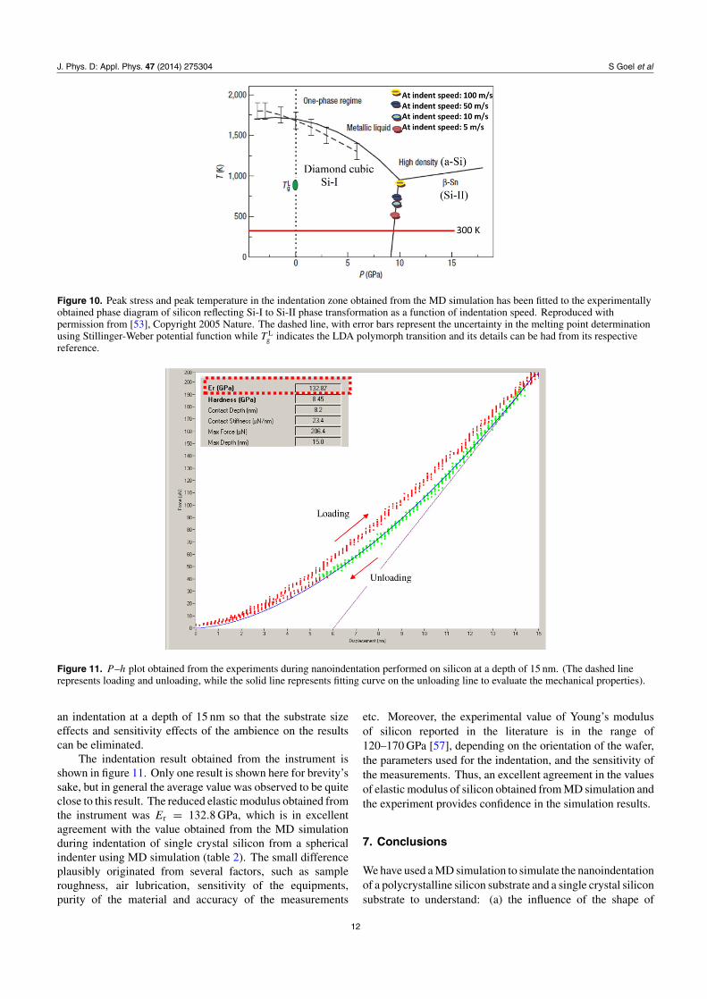
Figure 11. P –h plot obtained from the experiments during nanoindentation performed on silicon at a depth of 15 nm. (The dashed linerepresents loading and unloading, while the solid line represents fitting curve on the unloading line to evaluate the mechanical properties).
an indentation at a depth of 15 nm so that the substrate sizeeffects and sensitivity effects of the ambience on the resultscan be eliminated.
The indentation result obtained from the instrument isshown in figure 11. Only one result is shown here for brevity’ssake, but in general the average value was observed to be quiteclose to this result. The reduced elastic modulus obtained fromthe instrument was Er = 132.8 GPa, which is in excellentagreement with the value obtained from the MD simulationduring indentation of single crystal silicon from a sphericalindenter using MD simulation (table 2). The small differenceplausibly originated from several factors, such as sampleroughness, air lubrication, sensitivity of the equipments,purity of the material and accuracy of the measurements
etc. Moreover, the experimental value of Young’s modulusof silicon reported in the literature is in the range of120–170 GPa [57], depending on the orientation of the wafer,the parameters used for the indentation, and the sensitivity ofthe measurements. Thus, an excellent agreement in the valuesof elastic modulus of silicon obtained from MD simulation andthe experiment provides confidence in the simulation results.
7. Conclusions
We have used a MD simulation to simulate the nanoindentationof a polycrystalline silicon substrate and a single crystal siliconsubstrate to understand: (a) the influence of the shape of
12
J. Phys. D: Appl. Phys. 47 (2014) 275304 S Goel et al
the indenter (Berkovich pyramidal and spherical), and (b) therole of the crystal structure of silicon in influencing the stateof the HPPT, which induces the well-known Herzfeld–Motttransition in silicon. HPPT in silicon (Si-I to Si-II phasetransformation) was observed to be a common occurrencein all the cases, but its extent and the manner in whichit occurs differed significantly. The varying sub-surfacein a mechanically processed polysilicon arises due to thisphenomenon. The most significant result obtained from thesimulation was that the HPPT occurs more preferentially alongthe grain boundaries than across the grain boundaries. Thissingle phenomenon results in an increase of the transformationpressure to a significantly higher extent and, consequently,even the indentation forces were observed to increase. Theuse of an automated dislocation extraction algorithm (DXA)revealed no dislocations, thus confirming HPPT to be the solemechanism of plastic deformation of silicon in all the cases.Furthermore, HPPT appears to be a stress-dominated processrather than a thermally activated process and twinning appearsto be the mechanism underlying the occurrence of HPPT inbrittle materials (twinning resembles a quantum tunnellingprocess). The Oliver and Pharr method was extended tovalidate the simulation results and an excellent agreement wasfound between the MD simulation and the experiments.
Acknowledgments
The authors acknowledge funding support from the JohnMoyce Lessells travel scholarship from the Royal Societyof Edinburgh, International Research Fellowship account ofQueen’s University, Belfast and EPSRC research grant (Ref:EP/K018345/1) in undertaking this work. The authors wouldalso like to acknowledge the use of HPC service of STFCHartree Centre.
References
[1] Goel S, Agrawal A and Faisal N H 2014 Can a carbonnano-coating resist metallic phase transformation in siliconsubstrate during nanoimpact? Wear 315 38–41
[2] Yin L, Vancoille E Y J, Ramesh K and Huang H 2004 Surfacecharacterization of 6H-SiC (0 0 0 1) substrates inindentation and abrasive machining Int. J. Mach. ToolsManuf. 44 607–15
[3] Kovalchenko A, Gogotsi Y, Domnich V and Erdemir A 2002Phase transformations in silicon under dry and lubricatedsliding Tribol. Trans. 45 372–80
[4] Domnich V and Gogotsi Y 2002 Phase transformations insilicon under contact loading Rev. Adv. Mater. Sci 3 1–36
[5] Zarudi I, Zhang L, Cheong W and Yu T 2005 The difference ofphase distributions in silicon after indentation withBerkovich and spherical indenters Acta Mater. 53 4795–800
[6] Mylvaganam K, Zhang L, Eyben P, Mody J andVandervorst W 2009 Evolution of metastable phases insilicon during nanoindentation: mechanism analysis andexperimental verification Nanotechnology 20 305705
[7] Trenkle J C, Packard C E and Schuh C A 2010 Hotnanoindentation in inert environments Rev. Sci. Instrum.81 073901–13
[8] Gridneva I V, Milman Y V and Trefilov V I 1972 Phasetransition in diamond-structure crystals during hardnessmeasurements Phys. Status Solidi a 14 177–82
[9] Jamieson J C 1963 Crystal structures at high pressures ofmetallic modifications of silicon and germanium Science139 762–4
[10] Pizani P S, Jasinevicius R, Duduch J G and Porto A J V 1999Ductile and brittle modes in single-point-diamond-turningof silicon probed by Raman scattering J. Mater. Sci. Lett.18 1185–7
[11] Yan J 2004 Laser micro-Raman spectroscopy of single-pointdiamond machined silicon substrates J. Appl. Phys.95 2094–101
[12] Yan J W, Takahashi H, Tamaki J, Gai X and Kuriyagawa T2005 Transmission electron microscopic observation ofnanoindentations made on ductile-machined silicon wafersAppl. Phys. Lett. 87 211901
[13] Ge D, Domnich V and Gogotsi Y 2003 High-resolutiontransmission electron microscopy study of metastablesilicon phases produced by nanoindentation J. Appl. Phys.93 2418–23
[14] Goel S, Luo X, Reuben R L and Pen H 2012 Influence oftemperature and crystal orientation on tool wear duringsingle point diamond turning of silicon Wear284–285 65–72
[15] Goel S, Luo X and Reuben R L 2013 Wear mechanism ofdiamond tools against single crystal silicon in single pointdiamond turning process Tribol. Int. 57 272–81
[16] Budnitzki M and Kuna M 2012 A thermomechanicalconstitutive model for phase transformations in siliconunder pressure and contact loading conditions Int. J. SolidsStruct. 49 1316–24
[17] Vodenitcharova T and Zhang L 2004 A new constitutive modelfor the phase transformations in mono-crystalline siliconInt. J. Solids Struct. 41 5411–24
[18] Tadao K, Hirofumi H and Jiwang Y 2009 Finite elementmodeling of high-pressure deformation and phasetransformation of silicon beneath a sharp indenterSemicond. Sci. Technol. 24 025014
[19] Smith G, Tadmor E, Bernstein N and Kaxiras E 2001Multiscale simulations of silicon nanoindentation ActaMater. 49 4089–101
[20] Smith G, Tadmor E and Kaxiras E 2000 Multiscale simulationof loading and electrical resistance in siliconnanoindentation Phys. Rev. Lett. 84 1260
[21] Pen H M, Liang Y C, Luo X C, Bai Q S, Goel S andRitchie J M 2011 Multiscale simulation of nanometriccutting of single crystal copper and its experimentalvalidation Comput. Mater. Sci. 50 3431–41
[22] Sanz-Navarro C, Kenny S and Smith R 2004 Atomisticsimulations of structural transformations of silicon surfacesunder nanoindentation Nanotechnology 15 692
[23] Goel S, Faisal N H, Ratia V, Agrawal A and Stukowski A 2014Atomistic investigation on the structure–propertyrelationship during thermal spray nanoparticle impactComput. Mater. Sci. 84 163–74
[24] Goel S, Stukowski A, Goel G, Luo X and Reuben R L 2012Nanotribology at high temperatures Beilstein J.Nanotechnol. 3 586–8
[25] Cheong W C D and Zhang L C 2000 Molecular dynamicssimulation of phase transformations in silicon monocrystalsdue to nano-indentation Nanotechnology 11 173
[26] Sekine T and Kobayashi T 1997 Shock compression of 6Hpolytype SiC to 160 GPa Phys. Rev. B 55 8034
[27] Kim D and Oh S 2006 Atomistic simulation of structural phasetransformations in monocrystalline silicon induced bynanoindentation Nanotechnology 17 2259
[28] Lin Y H, Jian S R, Lai Y S and Yang P F 2008 Moleculardynamics simulation of nanoindentation-inducedmechanical deformation and phase transformationin monocrystalline silicon Nanoscale Res. Lett.3 71–5
13

J. Phys. D: Appl. Phys. 47 (2014) 275304 S Goel et al
[29] Wang Y, Ruffell S, Sears K, Knights A P, Bradby J E andWilliams J S 2010 Electrical properties of Si-XII and Si-IIIformed by nanoindentation Conf. on Optoelectronic andMicroelectronic Materials and Devices (COMMAD)(Canberra, ACT) pp 105–6
[30] Mylvaganam K and Zhang L C 2011 Nanotwinning inmonocrystalline silicon upon nanoscratching Scr. Mater.65 214–6
[31] Jang J-i, Lance M, Wen S, Tsui T Y and Pharr G 2005Indentation-induced phase transformations in silicon:influences of load, rate and indenter angle on thetransformation behavior Acta Mater. 53 1759–70
[32] Clarke D R, Kroll M C, Kirchner P D, Cook R F andHockey B J 1988 Amorphization and conductivity of siliconand germanium induced by indentation Phys. Rev. Lett.60 2156–9
[33] Goel S, Stukowski A, Luo X, Agrawal A and Reuben R L 2013Anisotropy of single-crystal 3C–SiC during nanometriccutting Modelling Simul. Mater. Sci. Eng. 21 065004
[34] Plimpton S 1995 Fast parallel algorithms for short-rangemolecular dynamics J. Comput. Phys. 117 1–19
[35] Humphrey W, Dalke A and Schulten K 1996 VMD—visualmolecular dynamics J. Mol. Graph. 14 33–8
[36] Stukowski A 2010 Visualization and analysis of atomisticsimulation data with OVITO–the Open Visualization ToolModelling Simul. Mater. Sci. Eng. 18 015012
[37] Stukowski A, Bulatov V V and Arsenlis A 2012 Automatedidentification and indexing of dislocations in crystalinterfaces Modelling Simul. Mater. Sci. Eng. 20 085007
[38] Goel S, Luo X, Anupam A and Stukowski A 2013 Effect of thecrystal structure in influencing the material removalmechanism during nanomachining of silicon J. Mech. Phys.Solids submitted
[39] Goel S, Luo X and Agrawal A 2014 Advances in diamondmachining of silicon through molecular dynamicssimulation and experiments Int. J. Mach. Tools Manuf.submitted
[40] Erhart P and Albe K 2005 Analytical potential for atomisticsimulations of silicon, carbon, and silicon carbide Phys.Rev. B 71 035211
[41] Cai M B, Li X P and Rahman M 2007 Study of the mechanismof nanoscale ductile mode cutting of silicon using moleculardynamics simulation Int. J. Mach. Tools Manuf. 47 75–80
[42] Cai M B, Li X P and Rahman M 2007 Characteristics of‘dynamic hard particles’ in nanoscale ductile mode cuttingof monocrystalline silicon with diamond tools in relation totool groove wear Wear 263 1459–66
[43] Wang Z, Liang Y, Chen M, Tong Z and Chen J 2010 Analysisabout diamond tool wear in nano-metric cutting of single
crystal silicon using molecular dynamics methodProc. SPIE 7655 765500
[44] Goel S, Joshi S S, Abdelal G and Agrawal A 2014 Moleculardynamics simulation of nanoindentation of Fe3C and Fe4CMater. Sci. Eng. A 597 331–41
[45] Choi Y, Van Vliet K J, Li J and Suresh S 2003 Size effects onthe onset of plastic deformation during nanoindentation ofthin films and patterned lines J. Appl. Phys. 94 6050–8
[46] Gannepalli A and Mallapragada S K 2001 Moleculardynamics studies of plastic deformation during siliconnanoindentation Nanotechnology 12 250
[47] Goel S, Yan J, Luo X and Agrawal A 2014 Incipient plasticityin 4H-SiC during quasistatic nanoindentation J. Mech.Behav. Biomed. Mater. 34 330–7
[48] Gouldstone A, Chollacoop N, Dao M, Li J, Minor A M andShen Y-L 2007 Indentation across size scales anddisciplines: Recent developments in experimentation andmodeling Acta Mater. 55 4015–39
[49] Gilman J J 1975 Flow of covalent solids at low temperaturesJ. Appl. Phys. 46 5110–3
[50] Goel S, Luo X, Reuben R L, Rashid W B and Ji N S 2012Simulation study of cutting forces, stresses and temperatureduring nanometric cutting of single crystal silicon Key Eng.Mater. 496 223–8.
[51] Gilman J J 2012 Twinning as a monoatomic phasetransformation www.micro.physics.ncsu.edu/ Accessed on1 October 2013
[52] Niihara K 1979 Slip systems and plastic deformation of siliconcarbide single crystals at high temperaturesJ. Less-Common Met. 65 155–66
[53] McMillan P F, Wilson M, Daisenberger D and Machon D 2005A density-driven phase transition between semiconductingand metalic polyamorhphs of silicon Nat. Mater. 4 680–4
[54] Oliver W C and Pharr G M 1992 Improved technique fordetermining hardness and elastic modulus using load anddisplacement sensing indentation experiments J. Mater. Res.7 1564–83
[55] Probe Selection Guide—Hysitron Triboindenter Manual,H. Incorporated, Editor. 2007 Minneapolis, USA
[56] Kruzic J J, Kim D K, Koester K J and Ritchie R O 2009Indentation techniques for evaluating the fracture toughnessof biomaterials and hard tissues J. Mech. Behav. Biomed.Mater. 2 384–95
[57] Luo X, Goel S and Reuben R L 2012 A quantitativeassessment of nanometric machinability of major polytypesof single crystal silicon carbide J. Eur. Ceram. Soc.32 3423–34
14


![New Boron and Silicon Free Single Crystal-Diffusion ... · crystal in a 〈110〉 direction [13, 14]. Figure 4: Light optical image of a typical Nanoindentation experiment with a](https://static.fdocuments.us/doc/165x107/6019ff966378335ffb018c39/new-boron-and-silicon-free-single-crystal-diffusion-crystal-in-a-110-direction.jpg)