MVE MURI 99 Kick-off Meeting R. Barker, Technical Monitor Started 1 May 99 October 1999 UC Davis...
21
MVE MURI 99 Kick-off Meeting R. Barker, Technical Monitor tarted 1 May 99 October 1999 UC Davis Millimeter Wave Vacuum/ Solid-State Hybrid Technologies S.A. Rosenau , C. Liang, W-K. Zhang (a) , C.C. Chang, K. Liu, C.W. Domier (a) , N.C. Luhmann, Jr., J.P. Heritage Department of Electrical and Computer Engineering, University of California, Davis, CA 95616 (a) Department of Applied Science, University of California, Davis, CA 95616
-
date post
20-Dec-2015 -
Category
Documents
-
view
214 -
download
0
Transcript of MVE MURI 99 Kick-off Meeting R. Barker, Technical Monitor Started 1 May 99 October 1999 UC Davis...

MVE MURI 99 Kick-off Meeting R. Barker, Technical Monitor
Started 1 May 99 October 1999
UC Davis Millimeter Wave Vacuum/ Solid-State Hybrid Technologies
S.A. Rosenau, C. Liang, W-K. Zhang(a), C.C. Chang, K. Liu, C.W. Domier(a), N.C. Luhmann, Jr., J.P. Heritage
Department of Electrical and Computer Engineering, University of California, Davis, CA 95616
(a) Department of Applied Science, University of California, Davis, CA 95616

MVE MURI 99 Kick-off Meeting R. Barker, Technical Monitor
Started 1 May 99 October 1999
Outline
• Frequency Multiplier Grid Arrays– Frequency Doubler Grid Arrays
– Frequency Tripler Grid Arrays
• Quasi-Optical Switch Arrays– High Speed Switch Arrays
– MEMS based Switch Array Power Control Array Tunable Filter
• Delay Line Controlled Phased Antenna Arrays
• Gated Silicon Field Emission Array Photocathodes

MVE MURI 99 Kick-off Meeting R. Barker, Technical Monitor
Started 1 May 99 October 1999
State-of-the-Art in High Power Sources
0.01
1
100
104
106
0.1 1 10 100 1000
Ave
rage
Pow
er (
W)
Klystron
Frequency (GHz)
Gridded TubeSolenold Focused
Coupled-Cavity TWT
Periodic Permanent Magnet Focused
Helix TWTStatic
InductionTransistor Si BJT
GaAs MESFET
Quasi-OpticalSolid State
Arrays
MPM
Gyrotron
Solid-state/ vacuum hybrid devices extend the state-of-the-art in both technology areas. Frequency multiplier grid arrays driven by MMPMs can provide 10 to 30 Woutput power at frequencies of 50 to 110 GHz.

MVE MURI 99 Kick-off Meeting R. Barker, Technical Monitor
Started 1 May 99 October 1999
Solid State–MVE Hybrid Devices and Configurations
The combination of novel layeredsemi-conductor device structures andphotonic crystals, together with thenewly developed microwave / millimeterwave power module (MPM / MMPM)promises revolutionary, compact highpower sources in the 30-300 GHz regionfor next generation DoD systems.
Output FIlter / Matching Element
Input Filter
Input Matching Element
Varactor Device
Antenna Lead
RF Input (f )o RF Output
(3f )o
AlN Cooling Plate
Photonic Band Gap (PBG) Waveguide Walls
Millimeter Wave Power Module
(MMPM)
Multiplier Array
Schematic of an MMPM Driving a Tripler Grid Array with a PBG Wall
Transition from Metal Waveguide to Overmoded PBG Waveguide
Transition from Overmoded PBG Waveguide to Metal Waveguide
Antenna Lead
MetalActive Regionn+
SubstrateIsolation
Top View Cross Sectional View
E
Back-to-Back Tripler Layout
E Field
Antenna Leads Back-to-Back
Varactor Diodes
V
C
C-V Curve
V
I
I-V Curve
Monolithic Frequency Tripler Array
MVE MURI 99 Kick-off Meeting R. Barker, Technical Monitor
Started 1 May 99 October 1999
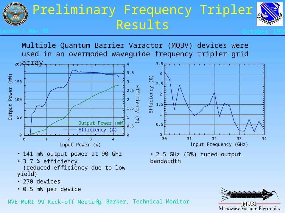
Preliminary Frequency Tripler Results
• 141 mW output power at 90 GHz• 3.7 % efficiency
(reduced efficiency due to low yield)• 270 devices• 0.5 mW per device
• 2.5 GHz (3%) tuned output bandwidth
Multiple Quantum Barrier Varactor (MQBV) devices were used in an overmoded waveguide frequency tripler grid array.
0
0.5
1
1.5
2
2.5
3
3.5
30 31 32 33 34
Effi
cie
ncy
(%
)Input Frequency (GHz)
0
50
100
150
200
0
0.5
1
1.5
2
2.5
3
3.5
4
0 1 2 3 4
Output Power (mW)
Efficiency (%)
Ou
tpu
t Po
we
r (m
W)
Efficie
ncy (%
)Input Power (W)

MVE MURI 99 Kick-off Meeting R. Barker, Technical Monitor
Started 1 May 99 October 1999
Schottky Varactor Devices
• Frequency doubler grid arrays using Schottky varactors fabricated by Martin-Marietta have been tested.
• Cmin = 15 fF, Cmax = 60 fF resulting in Cmax/Cmin = 4
• Rs = Rdiode + Rstrip = 6 Ω
L strip
ba
___ C diode
b
a___ R diode
C parasitic
Rstrip
C bias
1
2

MVE MURI 99 Kick-off Meeting R. Barker, Technical Monitor
Started 1 May 99 October 1999
Preliminary Frequency Doubler Results
• 410 mW output power at 66 GHz• 6.7 % efficiency at 63 GHz
(reduced efficiency due to fixturing)• 56 devices• 7.3 mW per device
• 6.6 GHz (10%) tuned output bandwidth• 3.6 GHz (6%) instantaneous output
bandwidth
Schottky diodes, fabricated by Martin-Marietta (Baltimore), were used in an overmoded waveguide frequency doubler grid array.
0
1
2
3
4
5
6
7
30 31 32 33 34 35
Instantaneous Tuned
Effi
cie
ncy
(%
)Input Frequency (GHz)
0
0.1
0.2
0.3
0.4
0
2
4
6
8
10
12
14
0 1 2 3 4 5 6 7 8
Output Power EfficiencySimulated Efficency
Ou
tpu
t Po
we
r (W
)
Efficie
ncy (%
)
Input Power (W)

MVE MURI 99 Kick-off Meeting R. Barker, Technical Monitor
Started 1 May 99 October 1999
State-of-the-Art in Moderate/High Power Frequency Multipliers

MVE MURI 99 Kick-off Meeting R. Barker, Technical Monitor
Started 1 May 99 October 1999
Quasi-Optical Switch Arrays
•Millimeter-wave switches may be used in a variety of applications, including
High speed, high power handling capability electronics control systems
for smart tubes and arrays
Millimeter-wave power control systems for klystrinos.
Moderate pulse radar reflectometry for plasma diagnostics
• Beam control array technology offers the possibility of achieving high speed and
high power handling capability with increased dynamic range.
• Silicon based microelectromechanical system (MEMS) switches have the potential
to form low cost, high performance, ultra wide quasi-optical control elements for
advanced defense and commercial applications.

MVE MURI 99 Kick-off Meeting R. Barker, Technical Monitor
Started 1 May 99 October 1999
High Speed Switch Array System
0
5
10
15
20
54 56 58 60 62 64 66
MeasuredSimulated
Co
ntr
ast
Rati
o (
dB
)
Frequency (GHz)High Speed Switch Array with Bias Control Board High Speed Switch Array Testing Results

MVE MURI 99 Kick-off Meeting R. Barker, Technical Monitor
Started 1 May 99 October 1999
Microwave / Millimeter Wave MEMS Power Control Array
MEMS Based Quasi-Optical Power Control ArraySEM Photo of Single MEMS Switch Device

MVE MURI 99 Kick-off Meeting R. Barker, Technical Monitor
Started 1 May 99 October 1999
Driver SourceDriver Source
KlystrinosKlystrinos
KlystrinosKlystrinos
KlystrinosKlystrinos
Power DividerHorn Antenna Array
MEMS NDLMEMS NDL
MEMS NDLMEMS NDL
MEMS NDLMEMS NDL
Klystrinos Controlled by MEMS Nonlinear Delay Lines

MVE MURI 99 Kick-off Meeting R. Barker, Technical Monitor
Started 1 May 99 October 1999
Design of MEMS based QO Tunable Filter
-100
-50
0
50
100
25 30 35 40 45
Phase of W-band Tunable filter
Tune 1Tune 2
-10
-8
-6
-4
-2
0
90 95 100 105 110
Pass-Band of Tunable Filter
Tune 1Tune 2
S2
1 (
dB
)
Frequency(GHz)
-20
-15
-10
-5
0
25 30 35 40 45
Stop-Band of Tunable Filter
Tune 1Tune 2
S21
(dB
)
The MEMS Tunable QO filter consists of several LC resonant circuits fabricated on each of the wafer surfaces. Simulations predict a W-band phase tunable filter with ~30 degree phase shift from 30 GHz to 40 GHz.
Simulation Result of W-band Tunable Filter
QO MEMS Tunable Filter System

MVE MURI 99 Kick-off Meeting R. Barker, Technical Monitor
Started 1 May 99 October 1999
• A V-band low insertion loss and high contrast ratio switch array has
been demonstrated, with a rise/fall time < 127 psec.
• A new class of GaAs based V-band and W-band high speed monolithic
millimeter wave switch array is being fabricated.
• MEMS Switch array technology is being developed. MEMS based
quasi-optical arrays will be employed as quasi-optical power control
arrays, quasi-optical phase shifters, and tunable quasi-optical filters.
Quasi-Optical Switch Array Accomplishments and Ongoing Activities

MVE MURI 99 Kick-off Meeting R. Barker, Technical Monitor
Started 1 May 99 October 1999
Wideband Delay Line Controlled Phased Antenna Array
• Microwave and millimeter wave phased antenna arrays are important elements for numerous applications, including satellite or ground communications, radar, imaging systems and plasma diagnostics.
• The use of diode loaded transmission lines as the broad-band phase controlling elements in phased antenna arrays has been successfully demonstrated in broadband and low loss beam steering and delay. [1] “Novel Low-Loss Delay Line for Broadband Phased Antenna Array Applications,” W-M, Zhang,et.al. IEEE Microwave and Guide Wave Letters,1997, [2] “A Hybrid Nonlinear Delay Line-based Broad-band Phased Antenna Array System,”R. Hsia,et.al. IEEE Microwave Guided Wave Letters 1998 [3] “Monolithic GaAs Phase Shifter Circuit with Low Insertion Loss and Continuous 0-360 Phase Shift at 20 GHz,” A. S. Nagra,et.al. IEEE Microwave Guided Wave Letters,1999

MVE MURI 99 Kick-off Meeting R. Barker, Technical Monitor
Started 1 May 99 October 1999
GaAs Nonlinear Delay Lines as Phase Control Elements of an MMPM Array
Widebandpower divider NDL
MMPM
MMPM
MMPM
MMPM
NDL
NDL
NDL
Driver
Wideband Antenna Array

MVE MURI 99 Kick-off Meeting R. Barker, Technical Monitor
Started 1 May 99 October 1999
Nonlinear Delay Lines
The line has a Bragg cutoff frequency given by:
))((
1
vCCLf
Diodelineline
Bragg
The equivalent circuit of a varactor diode periodically loaded Coplanar Waveguide (CPW) line is shown below:

MVE MURI 99 Kick-off Meeting R. Barker, Technical Monitor
Started 1 May 99 October 1999
1-Dimensional (1 x 8) LTSA Array Simulation
Beam scanning in E-plane1 x 8 linear tapered slot antenna array
Measured pattern
Simulated result
of proof-of-principle array
2.594061014
40
measured( )
s_array( )
9090 180
90 60 30 0 30 60 9040
35
30
25
20
15
10
5
0

MVE MURI 99 Kick-off Meeting R. Barker, Technical Monitor
Started 1 May 99 October 1999
Proof-of-Principle Nonlinear Delay Line Controlled Phased Antenna Array
-30
-25
-20
-15
-10
-5
0
-90 -60 -30 0 30 60 90
-3 V Bias (all channels)14 psec progressive delay14 psec progressive delay (reversed)
Rel
ativ
e Po
wer
(dB)
Angle (Þ)

MVE MURI 99 Kick-off Meeting R. Barker, Technical Monitor
Started 1 May 99 October 1999
6m center-to-center spacing, 2m gate aperture diameter, 2m tip height.
Bo
Microwave Circuitry
Collector
Gated Field Emission Cathode
ModulatedLaser Beam
Anode
Field emission does not require heating filament.
Optical gating avoids capacitive effect associated with electrical gating.
Prebunching capability reduces microwave circuitry and shortens tube length.
Shorter tube length requires fewer magnets for beam confinement.
Shorter tube length also increases efficiency.
Optical Prebunching in Microwave Tube
Micro-fabricated Field Emission Arrays
Anode
Emitted ElectronsGate Electrical Insulator
Emitter
1000V
0 – 200V
Illustration of Field Emitter with Biasing
Gated Silicon Field Emission Array Photocathodes
MVE MURI 99 Kick-off Meeting R. Barker, Technical Monitor
Started 1 May 99 October 1999
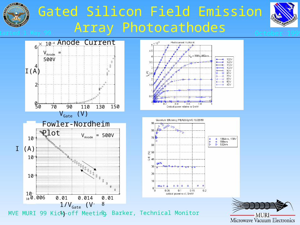
Anode Current
VGate (V)50 15070 90 110 1300
2
I(A)4
6 10-4
VAnode = 500V
0.006 0.01 0.014 0.018
1/VGate (V-1)
10-10
10-8
10-6
10-4VAnode = 500V
I (A)
Fowler-Nordheim Plot
Gated Silicon Field Emission Array Photocathodes