Multiple Output of Dual Half Bridge LLC Resonant … Output of Dual Half Bridge LLC Resonant...
8
Multiple Output of Dual Half Bridge LLC Resonant Converter Using PFM-PD Control Byeong Cheol Hyeon Student Member, IEEE National University of Seoul #043, San 56-1, Shillim-dong, Kwanak-Ku, Seoul, Korea [email protected] Bo Hyung Cho Senior Member, IEEE National University of Seoul #043, San 56-1, Shillim-dong, Kwanak-Ku, Seoul, Korea [email protected] Abstract -- This paper proposes the multiple output of dual half bridge LLC resonant converter using PFM-PD control. For the main output, dual half bridge LLC resonant converter controlled by pulse frequency modulation (PFM) is used. For the sub output, multiple outputs scheme is configured and operated by phase delay (PD) control. Since the control variables, PFM and PD, have little mutual effect, the sub output voltage can be regulated for a wide input and load range. All MOSFETs achieved ZVS and all rectifier diodes attained ZCS for the whole load range. The modes of operation are investigated and then steady state characteristics of the proposed converter are analyzed. A 320V- 400V input, 24V/20A, 5V/16A hardware prototype is realized with dsPIC33FJ16GS502 and tested to verify the performances of the proposed multiple output converters.. Index Terms— dual half bridge LLC resonant converter, multiple outputs, PFM-PD control, ZVS, ZCS. I. INTRODUCTION In general, since switched-mode power supply (SMPS) requires several converters, multiple output converter approach is the effective way for the high efficiency, small size and low cost. The important concern of the multiple output converter is the regulation of the various output voltages with less active and passive components. The use of cross regulation scheme is the cost effective method as no additional active elements are used; however, the regulation of the sub output voltage becomes loose under the light load [1-3]. With the weighted voltage control (WVC) method, all the output voltages are sensed using the weighting factors and controlled by the single switch [4-6]. This means that a voltage variation in one output is distributed to all the output voltages because there is a single control variable in the method. The synchronous switch post regulation (SSPR) scheme gives accurate output voltage regulation and easier over current protection by means of additional active switches [7-10]. In PWM-PFM control, one output voltage is controlled by pulse width modulation (PWM) and the other output voltage is regulated by pulse frequency modulation (PFM) [11-13]. Since two variables try to control the single switch, the operation range is highly restricted and it is applicable for the small power and lower input voltage. The multiple output converter with phase delay (PD) control has a simple structure and no active switch with tight output voltage regulation. The PWM-PD control scheme has been studied for used with flyback or forward converter, which is suitable for low power application. The PWM-PD control scheme for the high power and high input voltage application was two asymmetrical half bridge converters [14]. However, due to the asymmetrical PWM driving, each output voltage is affected by the others and the operation range of the multiple output converter is limited. This paper proposes the use of multiple output of dual half bridge LLC resonant converter using PFM-PD control. Due to the decreased mutual effect of the control variables in the sub output voltage gain, the tight regulation of all the output voltages can be achieved for the wide input and load range. Also, the proposed converters provide ZVS for all MOSFETs and ZCS for all the rectifier diodes regardless of the load current. The converter is investigated with an input voltage of 320V-400V and 24V/20A main output stage and 5.1V/16A sub output stage. Since an important object of this paper is focused on the operation and the regulation of the main and sub output stage, the operation and design of the main output stage makes reference to the previous studies of [15-17] and details will not be mentioned in the paper. In the next section, the basic operation principle of the PFM-PD control method is explained and the modes of operation are explored. And then, steady state characteristic such as peak current of the inductor and voltage gain of the sub stage are analyzed. A hardware prototype is built and tested using a digital control board with dsPIC33FJ16GS502 to confirm the performance of the proposed converter. II. THE PROPOSED MULTIPLE OUTPUTS DC/DC CONVERTER A. System Configuration and Operation Principles A circuit diagram of the proposed converter is shown in Fig.1. The converters are composed of two parts for the two output voltages. The stage for the main output voltage, v O_M , is controlled by PFM method and the stage for the sub output voltage, v O_S , is operated by PD method. Although all half bridge type topologies that are controlled by PFM can be a candidate for the main stage, LLC half bridge resonant converter is adopted due to the several advantages such as 1133 978-1-4244-2893-9/09/$25.00 ©2009 IEEE
Transcript of Multiple Output of Dual Half Bridge LLC Resonant … Output of Dual Half Bridge LLC Resonant...

Multiple Output of Dual Half Bridge LLC Resonant Converter Using PFM-PD Control
Byeong Cheol Hyeon Student Member, IEEE
National University of Seoul #043, San 56-1, Shillim-dong,
Kwanak-Ku, Seoul, Korea [email protected]
Bo Hyung Cho Senior Member, IEEE
National University of Seoul #043, San 56-1, Shillim-dong,
Kwanak-Ku, Seoul, Korea [email protected]
Abstract -- This paper proposes the multiple output of dual half bridge LLC resonant converter using PFM-PD control. For the main output, dual half bridge LLC resonant converter controlled by pulse frequency modulation (PFM) is used. For the sub output, multiple outputs scheme is configured and operated by phase delay (PD) control. Since the control variables, PFM and PD, have little mutual effect, the sub output voltage can be regulated for a wide input and load range. All MOSFETs achieved ZVS and all rectifier diodes attained ZCS for the whole load range. The modes of operation are investigated and then steady state characteristics of the proposed converter are analyzed. A 320V- 400V input, 24V/20A, 5V/16A hardware prototype is realized with dsPIC33FJ16GS502 and tested to verify the performances of the proposed multiple output converters..
Index Terms— dual half bridge LLC resonant converter, multiple outputs, PFM-PD control, ZVS, ZCS.
I. INTRODUCTION In general, since switched-mode power supply (SMPS)
requires several converters, multiple output converter approach is the effective way for the high efficiency, small size and low cost. The important concern of the multiple output converter is the regulation of the various output voltages with less active and passive components.
The use of cross regulation scheme is the cost effective method as no additional active elements are used; however, the regulation of the sub output voltage becomes loose under the light load [1-3]. With the weighted voltage control (WVC) method, all the output voltages are sensed using the weighting factors and controlled by the single switch [4-6]. This means that a voltage variation in one output is distributed to all the output voltages because there is a single control variable in the method. The synchronous switch post regulation (SSPR) scheme gives accurate output voltage regulation and easier over current protection by means of additional active switches [7-10].
In PWM-PFM control, one output voltage is controlled by pulse width modulation (PWM) and the other output voltage is regulated by pulse frequency modulation (PFM) [11-13]. Since two variables try to control the single switch, the operation range is highly restricted and it is applicable for the small power and lower input voltage. The multiple output converter with phase delay (PD) control has a simple
structure and no active switch with tight output voltage regulation. The PWM-PD control scheme has been studied for used with flyback or forward converter, which is suitable for low power application. The PWM-PD control scheme for the high power and high input voltage application was two asymmetrical half bridge converters [14]. However, due to the asymmetrical PWM driving, each output voltage is affected by the others and the operation range of the multiple output converter is limited.
This paper proposes the use of multiple output of dual half bridge LLC resonant converter using PFM-PD control. Due to the decreased mutual effect of the control variables in the sub output voltage gain, the tight regulation of all the output voltages can be achieved for the wide input and load range. Also, the proposed converters provide ZVS for all MOSFETs and ZCS for all the rectifier diodes regardless of the load current. The converter is investigated with an input voltage of 320V-400V and 24V/20A main output stage and 5.1V/16A sub output stage. Since an important object of this paper is focused on the operation and the regulation of the main and sub output stage, the operation and design of the main output stage makes reference to the previous studies of [15-17] and details will not be mentioned in the paper. In the next section, the basic operation principle of the PFM-PD control method is explained and the modes of operation are explored. And then, steady state characteristic such as peak current of the inductor and voltage gain of the sub stage are analyzed. A hardware prototype is built and tested using a digital control board with dsPIC33FJ16GS502 to confirm the performance of the proposed converter.
II. THE PROPOSED MULTIPLE OUTPUTS DC/DC CONVERTER
A. System Configuration and Operation Principles A circuit diagram of the proposed converter is shown in
Fig.1. The converters are composed of two parts for the two output voltages. The stage for the main output voltage, vO_M, is controlled by PFM method and the stage for the sub output voltage, vO_S, is operated by PD method. Although all half bridge type topologies that are controlled by PFM can be a candidate for the main stage, LLC half bridge resonant converter is adopted due to the several advantages such as
1133978-1-4244-2893-9/09/$25.00 ©2009 IEEE
2H _ MD
O _ Sv
1HS1LS
2HS2LS
H _ SD
L _ SD
O _ SC O _ SR
O _ MC O _ MR1H _ MD
1L _ MD
2L _ MD
A Bgv
2HS
2LS
1HS
1LS
1m _ ML
2rL
2rC
2m _ ML
lkL
m _ SL
1 1Pn : :
1 1Pn : :
1rC
1rL
1 1Sn : :
m _ SLiDH _ Si
DL _ Si
O _ Mv
1DH _ Mi
1DL _ Mi
2DH _ Mi
2DL _ Mi
1rLi
2rLi
1m _ MLi
2m _ MLi
ABv
m _ SLv
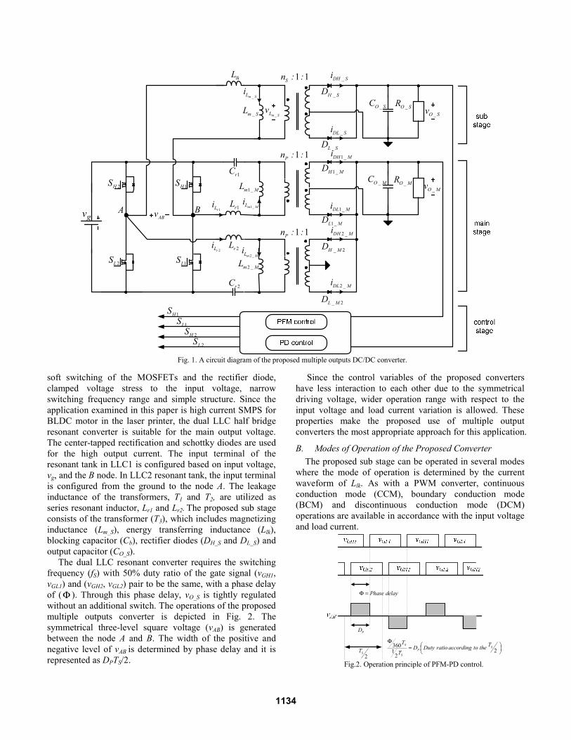
Fig. 1. A circuit diagram of the proposed multiple outputs DC/DC converter.
soft switching of the MOSFETs and the rectifier diode, clamped voltage stress to the input voltage, narrow switching frequency range and simple structure. Since the application examined in this paper is high current SMPS for BLDC motor in the laser printer, the dual LLC half bridge resonant converter is suitable for the main output voltage. The center-tapped rectification and schottky diodes are used for the high output current. The input terminal of the resonant tank in LLC1 is configured based on input voltage, vg, and the B node. In LLC2 resonant tank, the input terminal is configured from the ground to the node A. The leakage inductance of the transformers, T1 and T2, are utilized as series resonant inductor, Lr1 and Lr2. The proposed sub stage consists of the transformer (T3), which includes magnetizing inductance (Lm_S), energy transferring inductance (Llk), blocking capacitor (Cb), rectifier diodes (DH_S and DL_S) and output capacitor (CO_S).
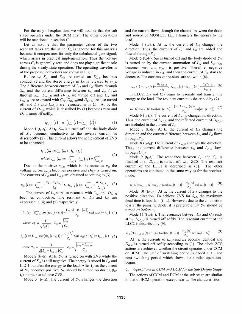
The dual LLC resonant converter requires the switching frequency (fS) with 50% duty ratio of the gate signal (vGH1, vGL1) and (vGH2, vGL2) pair to be the same, with a phase delay of (Φ ). Through this phase delay, vO_S is tightly regulated without an additional switch. The operations of the proposed multiple outputs converter is depicted in Fig. 2. The symmetrical three-level square voltage (vAB) is generated between the node A and B. The width of the positive and negative level of vAB is determined by phase delay and it is represented as DPTS/2.
Since the control variables of the proposed converters have less interaction to each other due to the symmetrical driving voltage, wider operation range with respect to the input voltage and load current variation is allowed. These properties make the proposed use of multiple output converters the most appropriate approach for this application.
B. Modes of Operation of the Proposed Converter The proposed sub stage can be operated in several modes
where the mode of operation is determined by the current waveform of Llk. As with a PWM converter, continuous conduction mode (CCM), boundary conduction mode (BCM) and discontinuous conduction mode (DCM) operations are available in accordance with the input voltage and load current.
Phase delayΦ =
36021
2
SS
P
S
T TD Duty ratio according to theT
Φ⎛ ⎞= ⎜ ⎟⎝ ⎠
PD
2ST
Fig.2. Operation principle of PFM-PD control.
1134
For the easy of explanation, we will assume that the sub stage operates under the BCM first. The other operations will be mentioned in section C.
Let us assume that the parameter values of the two resonant tanks are the same. Cb is ignored for this analysis because it compensates for only the unbalanced gate signal, which arises in practical implementation. Thus the voltage across Cb is generally zero and does not play significant role during the steady state operation. The operating waveforms of the proposed converters are shown in Fig. 3.
Before t0: SH1 and SH2 are turned on DL_S becomes conductive and the stored energy in Llk is released to vO_S. The difference between current of Lr2 and Llk flows through SH2 and the current difference between Lr1 and Llk flows through SH1. DH1_M and DL1_M are turned off and Lr1 and Lm1_M are resonated with Cr1. DH2_M and DL1_M are also turned off and Lr2 and Lm2_M are resonated with Cr1. At t0, the current of DL_S, which is described by (1) becomes zero and DL_S, turns off softly.
( ) ( ) ( )( )L _ S S lk m _ SD L Li t n i t i t= − (1)
Mode 1 (t0-t1): At t0, SH1 is turned off and the body diode of SL1 becomes conductive to the reverse current as describedby (2). This current allows the achievement of ZVS to be enhanced.
( ) ( ) ( )
( ) ( )1 1
1 1
0 0 0
0 0
L lk rpeak peak
lk rm _ S m _ M
S L L
L LL L
i t i t i t
where i t i , i t i
= −
= − = (2)
Due to the positive vAB, which is the same as vg, the voltage across Lm_S becomes positive and DH_S is turned on. The currents of Llk and Lm_S are obtained according to (3).
( ) ( )peak peakS O _ S S O _ S
lk m _ SL Lm _ S m _ S
gL L
lk m _ S
v n v n vi t i t , i t i t
L L−
= − + = − + (3)
The current of Lr1 starts to resonate with Cr1, and DL1_M becomes conductive. The resonant of Lr1 and Lr2 are expressed in (4) and (5) respectively.
( ) ( )( ) ( )( ) ( )( )1
1 1
001 0 01 0
01
101 01
11 1
2
1
r
r m _ M
g CpeakL L
r
rr r
v v ti t i cos t t sin t t
Z
Lwhere , ZCL C
−= − − −
= =
ω ω
ω
(4)
( ) ( ) ( )( ) ( ) ( )( ) ( )
( )
2
2 22 0
002 0 02 0
2
2 202 02
22 2 2
1
r
r m _ Mr
CL LL t
r m _ M
rr m _ M r
v ti t i cos t t sin t t i t
Z
L Lwhere , Z
CL L C
= ω − + ω − =
+ω = =
+
(5)
Mode 2 (t1-t2): At t1, SL1 is turned on with ZVS while the current of SL1 is still negative. The energy is stored in Llk and LLC1 transfers the energy to the load. After t2, as the current of SL1 becomes positive, SL1 should be turned on during (t0-t1) in order to achieve ZVS.
Mode 3 (t2-t3): The current of SL1 changes the direction
and the current flows through the channel between the drain and source of MOSFET. LLC1 transfers the energy to the load.
Mode 4 (t3-t4): At t3, the current of Lr1 changes the direction. Thus, the currents of Lr1 and Llk are added and flowed through SL1.
Mode 5 (t4-t5): SH2 is turned off and the body diode of SL2 is turned on by the current summation of Lr2 and Llk. vAB becomes zero and vLm_S is positive. Therefore, negative voltage is induced in Llk, and then the current of Llk starts to decrease. The currents expressions are shown in (6).
( ) ( ) ( ) ( )2 2S O _ S S O _ S
lk lk m _ S m _ SL L L Llk m _ S
n v n vi t i t , i t i t t
L L= − = + (6)
In LLC2, Lr2 and Cr2 begin to resonate and transfer the energy to the load. The resonant current is described by (7).
( ) ( ) ( )( ) ( )( ) ( )( )2 22 2 2 02 2 02 2
02
2 CrgLr Lm
v v ti t i t cos t t sin t t
Z
−= − − −ω ω (7)
Mode 6 (t5-t6): The current of Lm1_M changes its direction. Thus, the current of Lm1_M and the reflected current of DL1_M are included in the current of Lr1.
Mode 7 (t6-t7): At t6, the current of Lr2 changes the direction and the current difference between Lr2 and Llk flows through SL2.
Mode 8 (t7-t8): The current of Lm_S changes the direction. Thus, the current difference between Llk and Lm_S flows through DL_S.
Mode 9 (t8-t9): The resonance between Lr1 and Cr1 is finished at t8. DL1_M is turned off with ZCS. The resonant current of the LLC1 is described as (8). The other operations are continued in the same way as for the previous mode.
( ) ( ) ( ) ( )( ) ( ) ( )( )11 1 1
33 01 3 01 3
01
rr m _ M r
CL L L
v ti t i t i t cos t t sin t t
Z= = ω − + ω − (8)
Mode 10 (t9-t10): At t9, the current of SL2 changes to the positive direction. To achieve ZVS for SL2, the maximum dead time is less than (t4-t9). However, due to the conduction loss at the parasitic diode, it is preferable that SL2 should be turned on before t5.
Mode 11 (t10-t11): The resonance between Lr2 and Cr2 ends at t10. DL2_M is turned off softly. The resonant current of the LLC2 is described by (9).
( ) ( ) ( ) ( )( ) ( ) ( )( )22 2 2
55 02 5 02 5
02
rr m _ M r
CL L L
v ti t i t i t cos t t sin t t
Z= = ω − + ω − (9)
At t11, the currents of Lm_S and Llk become identical and DH_S is turned off softly according to (1). The diode ZCS actions are achieved whether the circuit operates under CCM or BCM. The half of switching period is ended at t11 and next switching period which shows the similar operations begins.
C. Operations in CCM and DCM for the Sub Output Stage The actions of CCM and DCM at the sub stage are similar
to that of BCM operation except near t0. The characteristics
1135
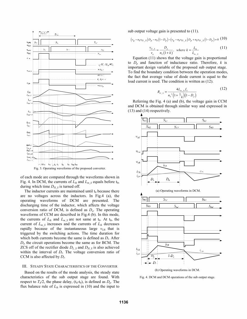
Fig. 3. Operating waveforms of the proposed converter.
of each mode are compared through the waveforms shown in Fig. 4. In DCM, the currents of Llk and Lm_S equals before t0, during which time DH_S is turned off.
The inductor currents are maintained until t0 because there are no voltages across the inductors. In Fig.4 (a), the operating waveforms of DCM are presented. The discharging time of the inductor, which affects the voltage conversion ratio of DCM, is defined as Da. The operating waveforms of CCM are described in Fig.4 (b). In this mode, the currents of Llk and Lm_S are not same at t0. At t0, the current of Lm_S increases and the currents of Llk decreases rapidly because of the instantaneous large vLlk that is triggered by the switching actions. The time duration for which both currents become the same is defined as Dl. After Dl, the circuit operations become the same as for BCM. The ZCS off of the rectifier diode DL_S and DH_S is also achieved within the interval of Dl. The voltage conversion ratio of CCM is also affected by Dl.
III. STEADY STATE CHARACTERISTICS OF THE CONVERTER Based on the results of the mode analysis, the steady state
characteristics of the sub output stage are found. With respect to TS/2, the phase delay, (t4-t0), is defined as Dp. The flux balance rule of Llk is expressed in (10) and the input to
sub output voltage gain is presented to (11).
( ) ( ) ( ) ( )1 1 0g S O _ S p S p g S O _ S p S O _ S pv n v D n D v n v D n v D− − − − − + − = (10)
( )1O _ S p lk
g S m _ S
v D L, where kv n k L
= =+
(11)
Equation (11) shows that the voltage gain is proportional to Dp and function of inductance ratio. Therefore, k is important design variable of the proposed sub output stage. To find the boundary condition between the operation modes, the fact that average value of diode current is equal to the load current is used. The condition is written as (12).
( )( )2
411 1
m _ S SO _ S
S p
L fR
n Dk=
+ −
(12)
Referring the Fig. 4 (a) and (b), the voltage gain in CCM and DCM is obtained through similar way and expressed in (13) and (14) respectively.
(a) Operating waveforms in DCM.
(b) Operating waveforms in DCM.
Fig. 4. DCM and DCM operations of the sub output stage.
1136
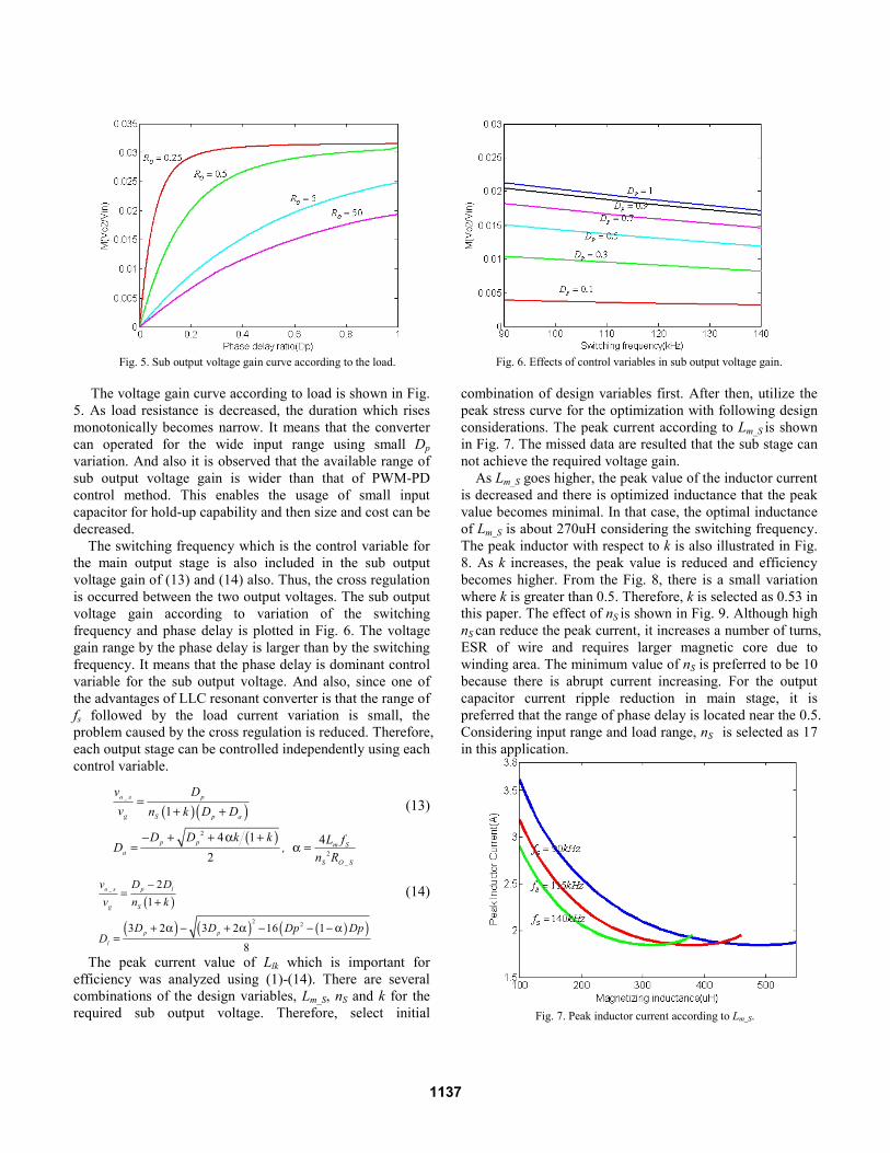
Fig. 5. Sub output voltage gain curve according to the load.
The voltage gain curve according to load is shown in Fig.
5. As load resistance is decreased, the duration which rises monotonically becomes narrow. It means that the converter can operated for the wide input range using small Dp variation. And also it is observed that the available range of sub output voltage gain is wider than that of PWM-PD control method. This enables the usage of small input capacitor for hold-up capability and then size and cost can be decreased.
The switching frequency which is the control variable for the main output stage is also included in the sub output voltage gain of (13) and (14) also. Thus, the cross regulation is occurred between the two output voltages. The sub output voltage gain according to variation of the switching frequency and phase delay is plotted in Fig. 6. The voltage gain range by the phase delay is larger than by the switching frequency. It means that the phase delay is dominant control variable for the sub output voltage. And also, since one of the advantages of LLC resonant converter is that the range of fs followed by the load current variation is small, the problem caused by the cross regulation is reduced. Therefore, each output stage can be controlled independently using each control variable.
( )( )( )2
2
1
4 1 42
o _ s p
g S p a
p p m Sa
S O _ S
v Dv n k D D
D D k k L fD ,n R
=+ +
− + + α += α =
(13)
( )
( ) ( ) ( )( )2 2
21
3 2 3 2 16 1
8
o _ s p l
g S
p p
l
v D Dv n k
D D Dp DpD
−=
+
+ α − + α − − − α=
(14)
The peak current value of Llk which is important for efficiency was analyzed using (1)-(14). There are several combinations of the design variables, Lm_S, nS and k for the required sub output voltage. Therefore, select initial
Fig. 6. Effects of control variables in sub output voltage gain.
combination of design variables first. After then, utilize the peak stress curve for the optimization with following design considerations. The peak current according to Lm_S is shown in Fig. 7. The missed data are resulted that the sub stage can not achieve the required voltage gain.
As Lm_S goes higher, the peak value of the inductor current is decreased and there is optimized inductance that the peak value becomes minimal. In that case, the optimal inductance of Lm_S is about 270uH considering the switching frequency. The peak inductor with respect to k is also illustrated in Fig. 8. As k increases, the peak value is reduced and efficiency becomes higher. From the Fig. 8, there is a small variation where k is greater than 0.5. Therefore, k is selected as 0.53 in this paper. The effect of nS is shown in Fig. 9. Although high nS can reduce the peak current, it increases a number of turns, ESR of wire and requires larger magnetic core due to winding area. The minimum value of nS is preferred to be 10 because there is abrupt current increasing. For the output capacitor current ripple reduction in main stage, it is preferred that the range of phase delay is located near the 0.5. Considering input range and load range, nS is selected as 17 in this application.
Fig. 7. Peak inductor current according to Lm_S.
1137

Fig. 8. Peak inductor current according to Lm_S.
Fig. 9. Peak inductor current according to nS.
IV. EXPERIMENTAL VERIFICATION The 24V/20A, 5.1V/16A hardware prototype of the
proposed multiple outputs converter is implemented to Table I. To generate four gate drive signal which can be controlled by PFM and PD simultaneously, a digital control board with a dsPIC33FJ16GS502, which provides 16bit instruction set, a pulse resolution of 1.04ns and an operation speed of 40MIPS is used.
The steady state operations of the proposed multiple output converters are shown in Fig. 10, which are similar to the waveforms from Fig. 3 and Fig. 4 (b). The operation of dual LLC resonant converter under the maximum load is presented in Fig. 11. There is a 0.2A RMS difference between iLr1 and iLr2 because of a parameter discrepancy between the series resonant inductances and turns ratios of the each LLC converter. In spite of the parameter errors, dual LLC converters share the power at a rate of 47%:53% when the sub output stage is operated under the rated power. The achievement of ZVS of MOSFET under the light load (10%) of the main and sub output is confirmed by Fig. 12. The switch voltages became zero before the gate signal goes on state. The waveforms of ZCS off for the rectifier diode
are shown in Fig. 13. The analysis result that diode current goes to zero during Dl interval of the CCM sub stage is clearly shown. The waveforms of the steady state operation are obtained when the input voltage is 380V (nominal) and both load currents are at nominal. The experimental results for the regulation performance, which is a key issue in multiple output converters, are shown in Fig. 14 and Fig. 15. vo_S is regulated within 0.27V (5.3%) for the current variation of the sub stage, while the main output voltage, vo_M, changes less than 0.1V (0.5%) from the Fig. 14.
TABLE I
PARAMETERS OF THE HARDWARE PROTOTYPE Main stage Sub stage
vo_M 24V±5% vo_S 5.1V±2.5% io_M 20A io_S 16ALr1 , Lr2 43uH, 45uH Llk 133uHCr1 , Cr2 33nF/600V Cb 1uF/630VLm_M1 , Lm_M2 180uH, 185uH Lm_S 250uHnp 17(T) : 2(T) ns 17(T) : 1(T)Co_M 13mF Co_S 9.9mFT1, T2 EER4950s T3 EER4042sCommonInput voltage 320V – 400VMOSFET switches STW20NM50Rectifier diodes KCH30A10Controller IC dsPIC33FJ16GS502
Fig. 10. The steady state waveforms of the sub output stage.
Fig. 11. The operation of main output stage (dual LLC).
1138
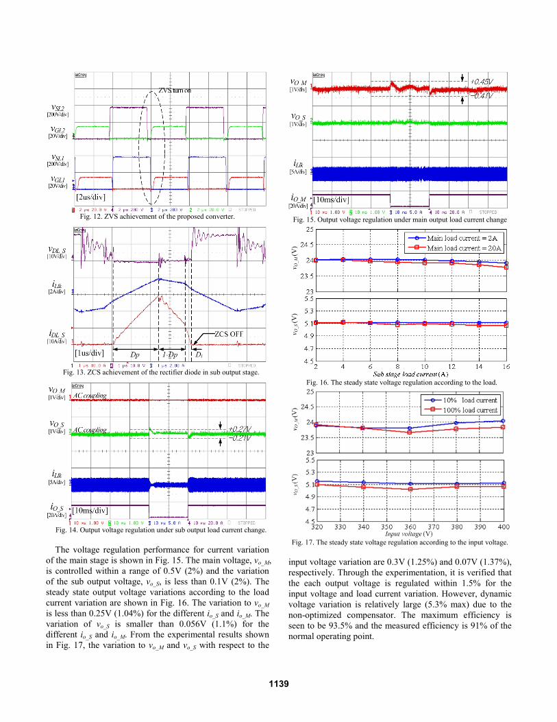
Fig. 12. ZVS achievement of the proposed converter.
Fig. 13. ZCS achievement of the rectifier diode in sub output stage.
Fig. 14. Output voltage regulation under sub output load current change.
The voltage regulation performance for current variation
of the main stage is shown in Fig. 15. The main voltage, vo_M, is controlled within a range of 0.5V (2%) and the variation of the sub output voltage, vo_S, is less than 0.1V (2%). The steady state output voltage variations according to the load current variation are shown in Fig. 16. The variation to vo_M is less than 0.25V (1.04%) for the different io_S and io_M. The variation of vo_S is smaller than 0.056V (1.1%) for the different io_S and io_M. From the experimental results shown in Fig. 17, the variation to vo_M and vo_S with respect to the
Fig. 15. Output voltage regulation under main output load current change
v O_S
(V)
v O_M
(V)
Fig. 16. The steady state voltage regulation according to the load.
Fig. 17. The steady state voltage regulation according to the input voltage. input voltage variation are 0.3V (1.25%) and 0.07V (1.37%), respectively. Through the experimentation, it is verified that the each output voltage is regulated within 1.5% for the input voltage and load current variation. However, dynamic voltage variation is relatively large (5.3% max) due to the non-optimized compensator. The maximum efficiency is seen to be 93.5% and the measured efficiency is 91% of the normal operating point.
1139

V. CONCLUSION This paper proposes the multiple outputs of dual half
bridge LLC resonant converters using PFM-PD Control. The steady state operations of the sub stage are analyzed and the design considerations are explained. The results of the peak stress investigation based on the steady state analysis are used to optimize the design procedure. The 480 W and 80 W hardware prototype was built for the verification of the proposed multiple output converters. In the experiment hardware, digital control board with dsPIC33FJ16GS502 is used. The experimental results show that steady state output voltages are regulated less than 1.4% against a 2A to 16A load variation and less than 1.5% against the 320V- 400V input voltage change. ZVS of MOSFET and ZCS of the rectifier diode are confirmed by the experimental results. The overall efficiency is of the proposed converters is 91% at the rated load. The proposed multiple output converters with PFM-PD control can be expanded to the n-phase frequency controlled converter with (n-1) sub stage configuration for the (n) output voltages.
REFERENCES [1] R. W. Erickson and D. Maksimovic, "A multiple-winding magnetics
model having directly measurable parameters," in Power Electronics Specialists Conference, 1998. PESC 98 Record. 29th Annual IEEE, 1998, pp. 1472-1478 vol.2.
[2] D. Maksimovic, R. W. Erickson, and C. Griesbach, "Modeling of cross-regulation in converters containing coupled inductors," Power Electronics, IEEE Transactions on, vol. 15, pp. 607-615, 2000.
[3] J. Chuanwen, M. Smith, Jr., K. M. Smedley, and K. King, "Cross regulation in flyback converters: analytic model and solution," Power Electronics, IEEE Transactions on, vol. 16, pp. 231-239, 2001.
[4] Y. T. Chen, D. Y. Chen, and Y. P. Wu, "Control-loop modeling of multiple-output feedback of forward converters," Power Electronics, IEEE Transactions on, vol. 8, pp. 320-328, 1993.
[5] C. Qing, F. C. Lee, and M. M. Jovanovic, "Small-signal analysis and design of weighted voltage control for a multiple-output forward converter," Power Electronics, IEEE Transactions on, vol. 10, pp. 589-596, 1995.
[6] L. Yu-Kang, Y. Shang-Chin, and S. Tzu-Herng, "Analysis and Design of a Double-Output Series-Resonant DC-DC Converter," Power Electronics, IEEE Transactions on, vol. 22, pp. 952-959, 2007.
[7] G. Levin, "A new secondary side post regulator (SSPR) PWM controller for multiple output power supplies," in Applied Power Electronics Conference and Exposition, 1995. APEC '95. Conference Proceedings 1995., Tenth Annual, 1995, pp. 736-742 vol.2.
[8] S. Havanur, "Combining synchronous rectification and post regulation for multiple isolated outputs," in Applied Power Electronics Conference and Exposition, 2004. APEC '04. Nineteenth Annual IEEE, 2004, pp. 872-877 vol.2.
[9] H. Yingyan, G. Yilei, C. Huiming, and Q. Zhaoming, "A novel multioutput forward-flyback converter with secondary side post regulation," in Power Electronics Specialists Conference, 2004. PESC 04. 2004 IEEE 35th Annual, 2004, pp. 618-621 Vol.1.
[10] L. Soung-Ju, K. Ho-Jin, L. Hai-Don, Y. Seung-Uk, C. Gyu-Ha, and M. Hyung-Soo, "A New Automatic Synchronous Switch Post Regulator for Multi-Output Converters," in Power Electronics Specialists Conference, 2006. PESC '06. 37th IEEE, 2006, pp. 1-4.
[11] J. Sebastian and J. Uceda, "The Double Converter: A Fully Regulated Two-Output DC-DC Converter," Power Electronics, IEEE Transactions on, vol. PE-2, pp. 239-246, 1987.
[12] H. E. Tacca, "Single-switch two-output flyback-forward converter operation," Power Electronics, IEEE Transactions on, vol. 13, pp. 903-911, 1998.
[13] J. Sebastian and J. Uceda, "An alternative method for controlling two-output DC-to-DC converters using saturable core inductor," Power Electronics, IEEE Transactions on, vol. 10, pp. 419-426, 1995.
[14] Z. Yanjun and X. Dehong, "Design and Implementation of an Accurately Regulated Multiple Output ZVS DC-DC Converter," Power Electronics, IEEE Transactions on, vol. 22, pp. 1731-1742, 2007.
[15] H. Choi, "Analysis and Design of LLC Resonant Converter with Integrated Transformer," in Applied Power Electronics Conference, APEC 2007 - Twenty Second Annual IEEE, 2007, pp. 1630-1635.
[16] T. Jin and K. Smedley, "Multiphase LLC Series Resonant Converter for Microprocessor Voltage Regulation," in Industry Applications Conference, 2006. 41st IAS Annual Meeting. Conference Record of the 2006 IEEE, 2006, pp. 2136-2143.
[17] Y. Kang-Hyun and M. Gun-Woo, "A Novel Two Phase Interleaved LLC Series Resonant Converter using a Phase of the Resonant Capacitor," JOURNAL OF POWER ELECTRONICS, vol. 8, pp. 275-279, 2008.
1140