Multilayer Microstrip Antenna for broadband Applications · of which is the microstrip patch...
5
International Journal of Science and Research (IJSR) ISSN (Online): 2319-7064 Index Copernicus Value (2013): 6.14 | Impact Factor (2013): 4.438 Volume 4 Issue 7, July 2015 www.ijsr.net Licensed Under Creative Commons Attribution CC BY Multilayer Microstrip Antenna for broadband Applications Rupesh Budharam Raut 1 , V.D.Nagrale 2 1 Department of Electronics and Telecommunication, AISSMS’s COE, Pune University, Pune, Maharashtra, India 2 Professor, Department of Electronics and Telecommunication, AISSMS’s COE, Pune University, Pune, Maharashtra, India Abstract: A novel broadband multilayer-layer coaxial coupled patch antenna is proposed. A simple patch geometry that is based on a rectangular patch which is place above the ground at a height (h 1 +h 2 ) fed by oaxialc coupled is introduced in this paper. A new resonant mode is excited using this novel patch structure. The results shows that the bandwidth is 450 to 750 GHz (S11<–10dB), larger than 40%. The gain is achieved to 4.65dB. The radiation patterns are similar and the gain can meet the demand for the communication applications over the operating frequency band. Simulation are done by using high Frequency Structure simulation (HFSS). Keywords: Coaxialc -coupled patch antenna; Multi-layer Broadband-band; Suspended microstrip antenna. 1. Introduction In order to meet the miniaturization requirements of portable communication equipment, researchers have given much attention recently to compact microstrip antennas. Many related compact designs with broadband dual-frequency operation, dual polarized radiation, circularly polarized radiation, and enhanced antenna gain have been reported. Many significant advances in improving the inherent narrow operating bandwidth of microstrip antennas have been published in the open literature since 1997. By using presently available techniques, one can easily achieve an impedance bandwidth (1:2 voltage standing wave ratios) of larger than 25% for a probe-fed single patch microstrip antenna. Other feeding methods such as the use of an aperture coupled feed, a capacitive coupled feed, and impedance bandwidths greater than 40% with good radiation. 1.1 Objective To design, simulate and fabricate broadband multilayer microstrip patch antenna operating at ISM band 2.4 GHz and study the effect on Impedance bandwidth after adding multilayer structure in microstrip antenna. 1.2 Scope The scope of this project is to study the basic multilayer antenna properties from several published papers and books, design a conventional rectangular microstrip antenna operating at 2.4GHz frequency. Comparing the results of conventional rectangular microstrip antenna and multilayer microstrip antenna. 2. Working Principle In telecommunication, there are several types of microstrip antennas (also known as printed antennas) the most common of which is the microstrip patch antenna or patch antenna. A patch antenna is a narrowband, wide-beam antenna fabricated by etching the antenna element pattern in metal trace bonded to an insulating dielectric substrate with a continuous metal layer bonded to the opposite side of the substrate which forms a ground plane. Microstrip or patch antennas are used widely within the mobile phone market because they are low cost, have a low profile and are easily fabricated. Consider the microstrip antenna shown in Figure 1, fed by a microstrip transmission line. The patch, microstrip and ground plane are made of high conductivity metal. The patch is of length L, width W, and sitting on top of a substrate (some dielectric circuit board) of thickness h with permittivity (ξ r ). The thickness of the ground plane or of the microstrip is not critically important. Typically the height h is much smaller than the wavelength of operation. Figure 1: Microstrip antenna From the below figure 1 it is observed that the total excited patch surface currents are increased, and the excited surface current distribution in the central portion of the radiating patch is also greatly enhanced for the proposed project design. As we change the shape of ground lane the surface current in that changes which in turn changes the return current on radiating patch. Due to this change in the surface current the change in radiation pattern, frequency of operation occurs. Hence by simply modifying ground plane we can miniaturize the antenna and there is no need to change the antenna if we want the antenna to be operated on other frequency. By modifying the ground planne the frequency of operation reduces means same antenna can work on lower frequency. That is anteena isize is reduce. Paper ID: SUB156377 454
Transcript of Multilayer Microstrip Antenna for broadband Applications · of which is the microstrip patch...
International Journal of Science and Research (IJSR) ISSN (Online): 2319-7064
Index Copernicus Value (2013): 6.14 | Impact Factor (2013): 4.438
Volume 4 Issue 7, July 2015
www.ijsr.net Licensed Under Creative Commons Attribution CC BY
Multilayer Microstrip Antenna for broadband
Applications
Rupesh Budharam Raut1, V.D.Nagrale
2
1 Department of Electronics and Telecommunication, AISSMS’s COE, Pune University, Pune, Maharashtra, India
2 Professor, Department of Electronics and Telecommunication, AISSMS’s COE, Pune University, Pune, Maharashtra, India
Abstract: A novel broadband multilayer-layer coaxial coupled patch antenna is proposed. A simple patch geometry that is based on a
rectangular patch which is place above the ground at a height (h1 +h2 ) fed by oaxialc coupled is introduced in this paper. A new
resonant mode is excited using this novel patch structure. The results shows that the bandwidth is 450 to 750 GHz (S11<–10dB), larger
than 40%. The gain is achieved to 4.65dB. The radiation patterns are similar and the gain can meet the demand for the communication
applications over the operating frequency band. Simulation are done by using high Frequency Structure simulation (HFSS).
Keywords: Coaxialc -coupled patch antenna; Multi-layer Broadband-band; Suspended microstrip antenna.
1. Introduction
In order to meet the miniaturization requirements of portable
communication equipment, researchers have given much
attention recently to compact microstrip antennas. Many
related compact designs with broadband dual-frequency
operation, dual polarized radiation, circularly polarized
radiation, and enhanced antenna gain have been reported.
Many significant advances in improving the inherent narrow
operating bandwidth of microstrip antennas have been
published in the open literature since 1997. By using
presently available techniques, one can easily achieve an
impedance bandwidth (1:2 voltage standing wave ratios) of
larger than 25% for a probe-fed single patch microstrip
antenna. Other feeding methods such as the use of an
aperture coupled feed, a capacitive coupled feed, and
impedance bandwidths greater than 40% with good radiation.
1.1 Objective
To design, simulate and fabricate broadband multilayer
microstrip patch antenna operating at ISM band 2.4 GHz and
study the effect on Impedance bandwidth after adding
multilayer structure in microstrip antenna.
1.2 Scope
The scope of this project is to study the basic multilayer
antenna properties from several published papers and books,
design a conventional rectangular microstrip antenna
operating at 2.4GHz frequency. Comparing the results of
conventional rectangular microstrip antenna and multilayer
microstrip antenna.
2. Working Principle
In telecommunication, there are several types of microstrip
antennas (also known as printed antennas) the most common
of which is the microstrip patch antenna or patch antenna. A
patch antenna is a narrowband, wide-beam antenna fabricated
by etching the antenna element pattern in metal trace bonded
to an insulating dielectric substrate with a continuous metal
layer bonded to the opposite side of the substrate which
forms a ground plane. Microstrip or patch antennas are used
widely within the mobile phone market because they are low
cost, have a low profile and are easily fabricated. Consider
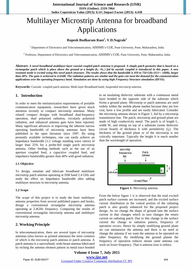
the microstrip antenna shown in Figure 1, fed by a microstrip
transmission line. The patch, microstrip and ground plane are
made of high conductivity metal. The patch is of length L,
width W, and sitting on top of a substrate (some dielectric
circuit board) of thickness h with permittivity (ξr). The
thickness of the ground plane or of the microstrip is not
critically important. Typically the height h is much smaller
than the wavelength of operation.
Figure 1: Microstrip antenna
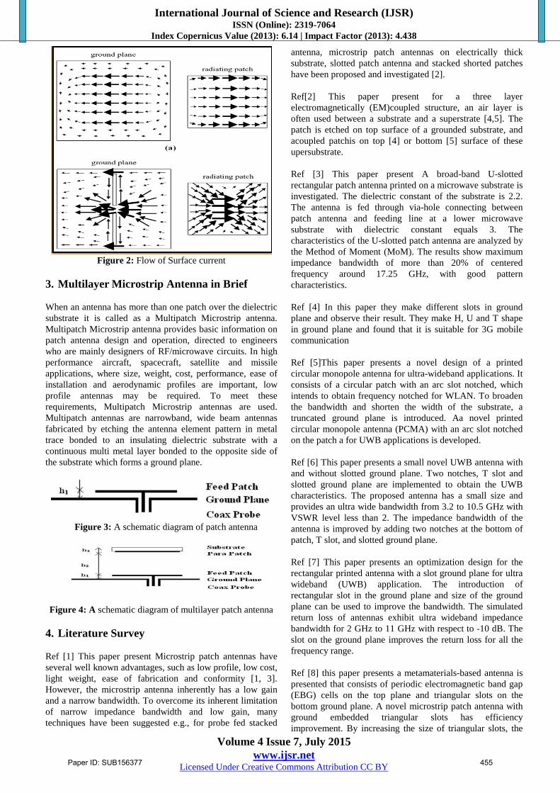
From the below figure 1 it is observed that the total excited
patch surface currents are increased, and the excited surface
current distribution in the central portion of the radiating
patch is also greatly enhanced for the proposed project
design. As we change the shape of ground lane the surface
current in that changes which in turn changes the return
current on radiating patch. Due to this change in the surface
current the change in radiation pattern, frequency of
operation occurs. Hence by simply modifying ground plane
we can miniaturize the antenna and there is no need to
change the antenna if we want the antenna to be operated on
other frequency. By modifying the ground planne the
frequency of operation reduces means same antenna can
work on lower frequency. That is anteena isize is reduce.
Paper ID: SUB156377 454
International Journal of Science and Research (IJSR) ISSN (Online): 2319-7064
Index Copernicus Value (2013): 6.14 | Impact Factor (2013): 4.438
Volume 4 Issue 7, July 2015
www.ijsr.net Licensed Under Creative Commons Attribution CC BY
Figure 2: Flow of Surface current
3. Multilayer Microstrip Antenna in Brief
When an antenna has more than one patch over the dielectric
substrate it is called as a Multipatch Microstrip antenna.
Multipatch Microstrip antenna provides basic information on
patch antenna design and operation, directed to engineers
who are mainly designers of RF/microwave circuits. In high
performance aircraft, spacecraft, satellite and missile
applications, where size, weight, cost, performance, ease of
installation and aerodynamic profiles are important, low
profile antennas may be required. To meet these
requirements, Multipatch Microstrip antennas are used.
Multipatch antennas are narrowband, wide beam antennas
fabricated by etching the antenna element pattern in metal
trace bonded to an insulating dielectric substrate with a
continuous multi metal layer bonded to the opposite side of
the substrate which forms a ground plane.
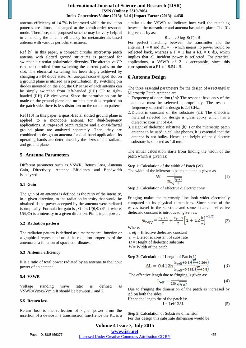
Figure 3: A schematic diagram of patch antenna
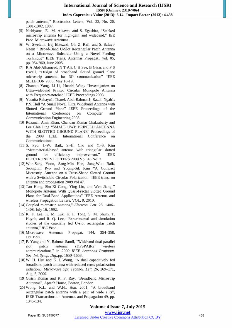
Figure 4: A schematic diagram of multilayer patch antenna
4. Literature Survey
Ref [1] This paper present Microstrip patch antennas have
several well known advantages, such as low profile, low cost,
light weight, ease of fabrication and conformity [1, 3].
However, the microstrip antenna inherently has a low gain
and a narrow bandwidth. To overcome its inherent limitation
of narrow impedance bandwidth and low gain, many
techniques have been suggested e.g., for probe fed stacked
antenna, microstrip patch antennas on electrically thick
substrate, slotted patch antenna and stacked shorted patches
have been proposed and investigated [2].
Ref[2] This paper present for a three layer
electromagnetically (EM)coupled structure, an air layer is
often used between a substrate and a superstrate [4,5]. The
patch is etched on top surface of a grounded substrate, and
acoupled patchis on top [4] or bottom [5] surface of these
upersubstrate.
Ref [3] This paper present A broad-band U-slotted
rectangular patch antenna printed on a microwave substrate is
investigated. The dielectric constant of the substrate is 2.2.
The antenna is fed through via-hole connecting between
patch antenna and feeding line at a lower microwave
substrate with dielectric constant equals 3. The
characteristics of the U-slotted patch antenna are analyzed by
the Method of Moment (MoM). The results show maximum
impedance bandwidth of more than 20% of centered
frequency around 17.25 GHz, with good pattern
characteristics.
Ref [4] In this paper they make different slots in ground
plane and observe their result. They make H, U and T shape
in ground plane and found that it is suitable for 3G mobile
communication
Ref [5]This paper presents a novel design of a printed
circular monopole antenna for ultra-wideband applications. It
consists of a circular patch with an arc slot notched, which
intends to obtain frequency notched for WLAN. To broaden
the bandwidth and shorten the width of the substrate, a
truncated ground plane is introduced. Aa novel printed
circular monopole antenna (PCMA) with an arc slot notched
on the patch a for UWB applications is developed.
Ref [6] This paper presents a small novel UWB antenna with
and without slotted ground plane. Two notches, T slot and
slotted ground plane are implemented to obtain the UWB
characteristics. The proposed antenna has a small size and
provides an ultra wide bandwidth from 3.2 to 10.5 GHz with
VSWR level less than 2. The impedance bandwidth of the
antenna is improved by adding two notches at the bottom of
patch, T slot, and slotted ground plane.
Ref [7] This paper presents an optimization design for the
rectangular printed antenna with a slot ground plane for ultra
wideband (UWB) application. The introduction of
rectangular slot in the ground plane and size of the ground
plane can be used to improve the bandwidth. The simulated
return loss of antennas exhibit ultra wideband impedance
bandwidth for 2 GHz to 11 GHz with respect to -10 dB. The
slot on the ground plane improves the return loss for all the
frequency range.
Ref [8] this paper presents a metamaterials-based antenna is
presented that consists of periodic electromagnetic band gap
(EBG) cells on the top plane and triangular slots on the
bottom ground plane. A novel microstrip patch antenna with
ground embedded triangular slots has efficiency
improvement. By increasing the size of triangular slots, the
Paper ID: SUB156377 455
International Journal of Science and Research (IJSR) ISSN (Online): 2319-7064
Index Copernicus Value (2013): 6.14 | Impact Factor (2013): 4.438
Volume 4 Issue 7, July 2015
www.ijsr.net Licensed Under Creative Commons Attribution CC BY
antenna efficiency of 14.7% is improved while the radiation
patterns are almost unchanged at the zeroth-order resonant
mode. Therefore, this proposed scheme may be very helpful
in enhancing the antenna efficiency for metamaterials-based
antenna with various periodic structures.
Ref [9] In this paper, a compact circular microstrip patch
antenna with slotted ground structures is proposed for
switchable circular polarization diversity. The alternative CP
can be controlled from switching the current paths on the
slot. The electrical switching has been simply achieved by
changing a PIN diode state. An unequal cross-shaped slot on
a ground plane is utilized as a perturbation. By switching pin
diodes mounted on the slot, the CP sense of each antenna can
be simply switched from left-handed (LH) CP to right-
handed (RH) CP vice versa. Since the perturbation can be
made on the ground plane and no bias circuit is required on
the patch side, there is less distortion on the radiation pattern
Ref [10] In this paper, a quasi-fractal slotted ground plane is
applied to a monopole antenna for dual-frequency
applications. A trapezoid patch radiator and a quasi-fractal
ground plane are analyzed separately. Then, they are
combined to design an antenna for dual-band application. Its
operating bands are determined by the sizes of the radiator
and ground plane.
5. Antenna Parameters
Different parameter such as VSWR, Return Loss, Antenna
Gain, Directivity, Antenna Efficiency and Bandwidth
isanalyzed.
5.1 Gain
The gain of an antenna is defined as the ratio of the intensity,
in a given direction, to the radiation intensity that would be
obtained if the power accepted by the antenna were radiated
isotropically. Formula for gain is , G=4π.U(θ,Ф) /Pin, where,
U(θ,Ф) is a intensity in a given direction, Pin is input power.
5.2 Radiation pattern
The radiation pattern is defined as a mathematical function or
a graphical representation of the radiation properties of the
antenna as a function of space coordinates.
5.3 Antenna efficiency
It is a ratio of total power radiated by an antenna to the input
power of an antenna.
5.4 VSWR
Voltage standing wave ratio is defined as
VSWR=Vmax/Vmin.It should lie between 1 and 2.
5.5 Return loss
Return loss is the reflection of signal power from the
insertion of a device in a transmission line.Hence the RL is a
similar to the VSWR to indicate how well the matching
between the transmitter and antenna has taken place. The RL
is given as by as:
RL= -20 log10(Γ) dB
For perfect matching between the transmitter and the
antenna, Γ = 0 and RL = ∞ which means no power would be
reflected back, whereas a Γ = 1 has a RL = 0 dB, which
implies that all incident power is reflected. For practical
applications, a VSWR of 2 is acceptable, since this
corresponds to a RL of -9.54 dB.
6. Antenna Design
The three essential parameters for the design of a rectangular
Microstrip Patch Antenna are:
1. Frequency of operation (f o): The resonant frequency of the
antenna must be selected appropriately. The resonant
frequency selected for design is 2.4 GHz.
2. Dielectric constant of the substrate (εr): The dielectric
material selected for design is glass epoxy which has a
dielectric constant of 4.4.
3. Height of dielectric substrate (h): For the microstrip patch
antenna to be used in cellular phones, it is essential that the
antenna is not bulky. Hence, the height of the dielectric
substrate is selected as 1.6 mm.
The initial calculation starts from finding the width of the
patch which is given as:
Step 1: Calculation of the width of Patch (W)
The width of the Microstrip patch antenna is given as
(1)
Step 2: Calculation of effective dielectric const
Fringing makes the microstrip line look wider electrically
compared to its physical dimensions. Since some of the
waves travel in the substrate and some in air, an effective
dielectric constant is introduced, given as:
(2)
Where,
εreff = Effective dielectric constant
εr = Dielectric constant of substrate
H = Height of dielectric substrate
W = Width of the patch
Step 3: Calculation of Length of Patch(L)
(3)
The effective length due to fringing is given as:
(4)
Due to fringing the dimension of the patch as increased by
ΔL on both the sides.
Hence the length the of the patch is:
L= Leff-2ΔL (5)
Step 5: Calculation of Substrate dimension
For this design this substrate dimension would be
Paper ID: SUB156377 456

International Journal of Science and Research (IJSR) ISSN (Online): 2319-7064
Index Copernicus Value (2013): 6.14 | Impact Factor (2013): 4.438
Volume 4 Issue 7, July 2015
www.ijsr.net Licensed Under Creative Commons Attribution CC BY
Ls=L+2*6h (6)
Ws=W+2*6h (7)
Step 6: Calculation of feed point
For this feed would be given L/4 distance.
Table 6.1: Calculated values for propose antenna Sr.No. Parameter Calculated value
1 W 58mm
2
3.99
3
45mm
4
0.75mm
5 L 45mm
6 L/4 11mm
7. Software Requirements
Ansoft HFSS
It is Debian based linux operating system, HFSS is the
industry standard simulation tool for 3D full wave
elcctromaganectic field simulation.HFSS provides E and H
fileld,current,S-parameter and near and far radiation fileds
results.Intrensic to the success of HFSS as an engineering
design tool is its automated solution process where users are
only required to specify geometry, material properties and
the desired output.With the help of HFSS we can
automatically generate an appropriate, efficient and accurate
mesh for solving the problem.
8. Results Analysis
Figure5: Multilayer Microstrip antenna for 2.4GHZ
Figure 6: Return loss of proposed microstrip antenna
Figure 7: VSWR of proposed microstrip antenna
Figure 8: Gain of proposed microstrip antenna
The value of VSWR as shown in figure 7 at 2.3GHz
frequency for multilayer patch antenna is 1.92 and banwidht
is 740MHz which very good for broadband applications.This
depicts that there is good impedance matching between inset-
fed microstrip transmission line and the rectangular radiating
element at the frequency 2.3GHz. Return loss is a measure
of impedance bandwidth for which the antenna is sufficiently
matched to its input transmission line such that 10% or less
of the incident signal is lost due to reflections. Impedance
bandwidth measurements include the characterization of the
Voltage Standing Wave Ratio (VSWR) and return loss
throughout the band of interest. From the return loss
performance antenna operating bandwidth extends 450 to
740 MHz and return loss are -12.9db to -16.22db as shown in
figure 6. The gain of the stated antenna was experimentally
obtained using Ansoft HFSS shown in figure 8. Maximum
measured gain of receiving antenna obtained is 4.65 db as
shown in figure 8.
9. Conclusion
A high gain Multilayer coaxial feed microstrip patch antenna
with gap-coupled mechanism has been investigated. The
proposed antenna has shown to possess two times increasing
gain as compared with that of the conventional microstrip
patch antenna. The resulting size of this antenna makes it
applicable for use in mobile handset application. The return
loss, input impedance matching is perfectly showing the
applicability of this antenna in the GPS applications.
References
[1] W. R. Jin, and J. Geng, 2008. “E-Shape patch with
wideband and circular polarization formillimeter-wave
communication”, IEEE Transactions on Antennas and
Propagation 56(3), pp.893-895.
[2] Pozar, D.M. and D.H., Schaubert, 1995. “Microstrip
antennas, the analysis and design of microstrip antennas
and arrays”, New York: IEEE press.[3] Pozar, D.M.,
1992. “Microstrip Antennas”, Proceeding IEEE 80.
[3] Wong, K.L. and W.H., Hsu, 2001. “A broadband
rectangular patch antenna with a pair of wide slits”,
IEEE Transactions on Antennas and Propagation 49, pp.
1345-1347.
[4] Lee, R. Q., K. F. Lee, and J. Bobinchak, “Characteristics
of a two-layer electromagnetically coupled rectangular
Paper ID: SUB156377 457
International Journal of Science and Research (IJSR) ISSN (Online): 2319-7064
Index Copernicus Value (2013): 6.14 | Impact Factor (2013): 4.438
Volume 4 Issue 7, July 2015
www.ijsr.net Licensed Under Creative Commons Attribution CC BY
patch antenna," Electronics Letters, Vol. 23, No. 20,
1301-1302, 1987.
[5] Nishiyama, E., M. Aikawa, and S. Egashira, “Stacked
microstrip antenna for high-gain and wideband," IEE
Proc. Microwave.Antennas.
[6] W. Swelamt, Iraj Ehtezazi, Gh. Z. Rafi, and S. Safavi-
Naein ” Broad-Band U-Slot Rectangular Patch Antenna
on a Microwave Substrate Using a Novel Feeding
Technique” IEEE Trans. Antennas Propagat., vol. 05,
pp. 954-960, June 2005.
[7] R A Abd-Alhameed, N T Ali, C H See, B Gizas and P S
Excell, “Design of broadband slotted ground plane
microstrip antenna for 3G communication” IEEE
MELECON 2006, May 16-19,
[8] Zhantao Yang, Li Li, Huazhi Wang “Investigation on
Ultra-wideband Printed Circular Monopole Antenna
with Frequency-notched” IEEE Proceedings 2008.
[9] Yusnita Rahayu1, Tharek Abd. Rahman1, Razali Ngah1,
P.S. Hall “A Small Novel Ultra Wideband Antenna with
Slotted Ground Plane” IEEE Proceedings of the
International Conference on Computer and
Communication Engineering 2008
[10] Rozanah Amir Khan, Chandan Kumar Chakrabarty and
Lee Chia Ping “SMALL UWB PRINTED ANTENNA
WITH SLOTTED GROUND PLANE” Proceedings of
the 2009 IEEE International Conference on
Communications
[11] S. Pyo, J.-W. Baik, S.-H. Cho and Y.-S. Kim
“Metamaterial-based antenna with triangular slotted
ground for efficiency improvement.” IEEE
ELECTRONICS LETTERS 2009 Vol. 45 No. 3
[12] Won-Sang Yoon, Sang-Min Han, Jung-Woo Baik,
Seongmin Pyo and Young-Sik Kim “A Compact
Microstrip Antenna on a Cross-Shape Slotted Ground
with a Switchable Circular Polarization “IEEE trans. on
antenna and propagation 2009 vol 47.
[13] Tao Hong, Shu-Xi Gong, Ying Liu, and Wen Jiang ”
Monopole Antenna With Quasi-Fractal Slotted Ground
Plane for Dual-Band Applications” IEEE Antenna and
wireless Propagation Letters, VOL. 9, 2010.
[14] Coupled microstrip antenna,” Electron. Lett. 28, 1406–
1408, July 16, 1992.
[15] K. F. Lee, K. M. Luk, K. F. Tong, S. M. Shum, T.
Huynh, and R. Q. Lee, “Experimental and simulation
studies of the coaxially fed U-slot rectangular patch
antenna,” IEE Proc.
[16] Microwave Antennas Propagat. 144, 354–358,
Oct.1997.
[17] F. Yang and Y. Rahmat-Samii, “Wideband dual parallel
slot patch antenna (DPSPA)for wireless
communications,” in 2000 IEEE Antennas Propagat.
Soc. Int. Symp. Dig.,pp. 1650–1653.
[18] W. H. Hsu and K. L.Wong, “A dual capacitively fed
broadband patch antenna with reduced cross-polarization
radiation,” Microwave Opt. Technol. Lett. 26, 169–171,
Aug. 5, 2000.
[19] Girish Kumar and K. P. Ray, “Broadband Microstrip
Antennas”, Aptech House, Boston, London.
[20] Wong, K.L. and W.H., Hsu, 2001. “A broadband
rectangular patch antenna with a pair of wide slits”,
IEEE Transactions on Antennas and Propagation 49, pp.
1345-134.
Paper ID: SUB156377 458